JP5079072B2 - Display device having optical sensor and driving method thereof - Google Patents
Display device having optical sensor and driving method thereof Download PDFInfo
- Publication number
- JP5079072B2 JP5079072B2 JP2010278883A JP2010278883A JP5079072B2 JP 5079072 B2 JP5079072 B2 JP 5079072B2 JP 2010278883 A JP2010278883 A JP 2010278883A JP 2010278883 A JP2010278883 A JP 2010278883A JP 5079072 B2 JP5079072 B2 JP 5079072B2
- Authority
- JP
- Japan
- Prior art keywords
- layer
- transistor
- oxide semiconductor
- display device
- optical sensor
- Prior art date
- Legal status (The legal status is an assumption and is not a legal conclusion. Google has not performed a legal analysis and makes no representation as to the accuracy of the status listed.)
- Active
Links
Images


Classifications
-
- G—PHYSICS
- G09—EDUCATION; CRYPTOGRAPHY; DISPLAY; ADVERTISING; SEALS
- G09G—ARRANGEMENTS OR CIRCUITS FOR CONTROL OF INDICATING DEVICES USING STATIC MEANS TO PRESENT VARIABLE INFORMATION
- G09G3/00—Control arrangements or circuits, of interest only in connection with visual indicators other than cathode-ray tubes
- G09G3/20—Control arrangements or circuits, of interest only in connection with visual indicators other than cathode-ray tubes for presentation of an assembly of a number of characters, e.g. a page, by composing the assembly by combination of individual elements arranged in a matrix no fixed position being assigned to or needed to be assigned to the individual characters or partial characters
- G09G3/34—Control arrangements or circuits, of interest only in connection with visual indicators other than cathode-ray tubes for presentation of an assembly of a number of characters, e.g. a page, by composing the assembly by combination of individual elements arranged in a matrix no fixed position being assigned to or needed to be assigned to the individual characters or partial characters by control of light from an independent source
- G09G3/3406—Control of illumination source
- G09G3/3413—Details of control of colour illumination sources
-
- G—PHYSICS
- G02—OPTICS
- G02F—OPTICAL DEVICES OR ARRANGEMENTS FOR THE CONTROL OF LIGHT BY MODIFICATION OF THE OPTICAL PROPERTIES OF THE MEDIA OF THE ELEMENTS INVOLVED THEREIN; NON-LINEAR OPTICS; FREQUENCY-CHANGING OF LIGHT; OPTICAL LOGIC ELEMENTS; OPTICAL ANALOGUE/DIGITAL CONVERTERS
- G02F1/00—Devices or arrangements for the control of the intensity, colour, phase, polarisation or direction of light arriving from an independent light source, e.g. switching, gating or modulating; Non-linear optics
- G02F1/01—Devices or arrangements for the control of the intensity, colour, phase, polarisation or direction of light arriving from an independent light source, e.g. switching, gating or modulating; Non-linear optics for the control of the intensity, phase, polarisation or colour
- G02F1/13—Devices or arrangements for the control of the intensity, colour, phase, polarisation or direction of light arriving from an independent light source, e.g. switching, gating or modulating; Non-linear optics for the control of the intensity, phase, polarisation or colour based on liquid crystals, e.g. single liquid crystal display cells
- G02F1/133—Constructional arrangements; Operation of liquid crystal cells; Circuit arrangements
- G02F1/13306—Circuit arrangements or driving methods for the control of single liquid crystal cells
- G02F1/13312—Circuits comprising photodetectors for purposes other than feedback
-
- G—PHYSICS
- G02—OPTICS
- G02F—OPTICAL DEVICES OR ARRANGEMENTS FOR THE CONTROL OF LIGHT BY MODIFICATION OF THE OPTICAL PROPERTIES OF THE MEDIA OF THE ELEMENTS INVOLVED THEREIN; NON-LINEAR OPTICS; FREQUENCY-CHANGING OF LIGHT; OPTICAL LOGIC ELEMENTS; OPTICAL ANALOGUE/DIGITAL CONVERTERS
- G02F1/00—Devices or arrangements for the control of the intensity, colour, phase, polarisation or direction of light arriving from an independent light source, e.g. switching, gating or modulating; Non-linear optics
- G02F1/01—Devices or arrangements for the control of the intensity, colour, phase, polarisation or direction of light arriving from an independent light source, e.g. switching, gating or modulating; Non-linear optics for the control of the intensity, phase, polarisation or colour
- G02F1/13—Devices or arrangements for the control of the intensity, colour, phase, polarisation or direction of light arriving from an independent light source, e.g. switching, gating or modulating; Non-linear optics for the control of the intensity, phase, polarisation or colour based on liquid crystals, e.g. single liquid crystal display cells
- G02F1/133—Constructional arrangements; Operation of liquid crystal cells; Circuit arrangements
- G02F1/13306—Circuit arrangements or driving methods for the control of single liquid crystal cells
- G02F1/13318—Circuits comprising a photodetector
-
- G—PHYSICS
- G09—EDUCATION; CRYPTOGRAPHY; DISPLAY; ADVERTISING; SEALS
- G09F—DISPLAYING; ADVERTISING; SIGNS; LABELS OR NAME-PLATES; SEALS
- G09F27/00—Combined visual and audible advertising or displaying, e.g. for public address
- G09F27/005—Signs associated with a sensor
-
- G—PHYSICS
- G09—EDUCATION; CRYPTOGRAPHY; DISPLAY; ADVERTISING; SEALS
- G09G—ARRANGEMENTS OR CIRCUITS FOR CONTROL OF INDICATING DEVICES USING STATIC MEANS TO PRESENT VARIABLE INFORMATION
- G09G3/00—Control arrangements or circuits, of interest only in connection with visual indicators other than cathode-ray tubes
- G09G3/20—Control arrangements or circuits, of interest only in connection with visual indicators other than cathode-ray tubes for presentation of an assembly of a number of characters, e.g. a page, by composing the assembly by combination of individual elements arranged in a matrix no fixed position being assigned to or needed to be assigned to the individual characters or partial characters
- G09G3/2003—Display of colours
-
- G—PHYSICS
- G09—EDUCATION; CRYPTOGRAPHY; DISPLAY; ADVERTISING; SEALS
- G09G—ARRANGEMENTS OR CIRCUITS FOR CONTROL OF INDICATING DEVICES USING STATIC MEANS TO PRESENT VARIABLE INFORMATION
- G09G3/00—Control arrangements or circuits, of interest only in connection with visual indicators other than cathode-ray tubes
- G09G3/20—Control arrangements or circuits, of interest only in connection with visual indicators other than cathode-ray tubes for presentation of an assembly of a number of characters, e.g. a page, by composing the assembly by combination of individual elements arranged in a matrix no fixed position being assigned to or needed to be assigned to the individual characters or partial characters
- G09G3/34—Control arrangements or circuits, of interest only in connection with visual indicators other than cathode-ray tubes for presentation of an assembly of a number of characters, e.g. a page, by composing the assembly by combination of individual elements arranged in a matrix no fixed position being assigned to or needed to be assigned to the individual characters or partial characters by control of light from an independent source
- G09G3/36—Control arrangements or circuits, of interest only in connection with visual indicators other than cathode-ray tubes for presentation of an assembly of a number of characters, e.g. a page, by composing the assembly by combination of individual elements arranged in a matrix no fixed position being assigned to or needed to be assigned to the individual characters or partial characters by control of light from an independent source using liquid crystals
- G09G3/3611—Control of matrices with row and column drivers
- G09G3/3648—Control of matrices with row and column drivers using an active matrix
-
- G—PHYSICS
- G09—EDUCATION; CRYPTOGRAPHY; DISPLAY; ADVERTISING; SEALS
- G09G—ARRANGEMENTS OR CIRCUITS FOR CONTROL OF INDICATING DEVICES USING STATIC MEANS TO PRESENT VARIABLE INFORMATION
- G09G3/00—Control arrangements or circuits, of interest only in connection with visual indicators other than cathode-ray tubes
- G09G3/20—Control arrangements or circuits, of interest only in connection with visual indicators other than cathode-ray tubes for presentation of an assembly of a number of characters, e.g. a page, by composing the assembly by combination of individual elements arranged in a matrix no fixed position being assigned to or needed to be assigned to the individual characters or partial characters
- G09G3/34—Control arrangements or circuits, of interest only in connection with visual indicators other than cathode-ray tubes for presentation of an assembly of a number of characters, e.g. a page, by composing the assembly by combination of individual elements arranged in a matrix no fixed position being assigned to or needed to be assigned to the individual characters or partial characters by control of light from an independent source
- G09G3/36—Control arrangements or circuits, of interest only in connection with visual indicators other than cathode-ray tubes for presentation of an assembly of a number of characters, e.g. a page, by composing the assembly by combination of individual elements arranged in a matrix no fixed position being assigned to or needed to be assigned to the individual characters or partial characters by control of light from an independent source using liquid crystals
- G09G3/3611—Control of matrices with row and column drivers
- G09G3/3696—Generation of voltages supplied to electrode drivers
-
- G—PHYSICS
- G02—OPTICS
- G02F—OPTICAL DEVICES OR ARRANGEMENTS FOR THE CONTROL OF LIGHT BY MODIFICATION OF THE OPTICAL PROPERTIES OF THE MEDIA OF THE ELEMENTS INVOLVED THEREIN; NON-LINEAR OPTICS; FREQUENCY-CHANGING OF LIGHT; OPTICAL LOGIC ELEMENTS; OPTICAL ANALOGUE/DIGITAL CONVERTERS
- G02F1/00—Devices or arrangements for the control of the intensity, colour, phase, polarisation or direction of light arriving from an independent light source, e.g. switching, gating or modulating; Non-linear optics
- G02F1/01—Devices or arrangements for the control of the intensity, colour, phase, polarisation or direction of light arriving from an independent light source, e.g. switching, gating or modulating; Non-linear optics for the control of the intensity, phase, polarisation or colour
- G02F1/13—Devices or arrangements for the control of the intensity, colour, phase, polarisation or direction of light arriving from an independent light source, e.g. switching, gating or modulating; Non-linear optics for the control of the intensity, phase, polarisation or colour based on liquid crystals, e.g. single liquid crystal display cells
- G02F1/133—Constructional arrangements; Operation of liquid crystal cells; Circuit arrangements
- G02F1/136—Liquid crystal cells structurally associated with a semi-conducting layer or substrate, e.g. cells forming part of an integrated circuit
- G02F1/1362—Active matrix addressed cells
- G02F1/1368—Active matrix addressed cells in which the switching element is a three-electrode device
-
- G—PHYSICS
- G09—EDUCATION; CRYPTOGRAPHY; DISPLAY; ADVERTISING; SEALS
- G09G—ARRANGEMENTS OR CIRCUITS FOR CONTROL OF INDICATING DEVICES USING STATIC MEANS TO PRESENT VARIABLE INFORMATION
- G09G2300/00—Aspects of the constitution of display devices
- G09G2300/04—Structural and physical details of display devices
- G09G2300/0421—Structural details of the set of electrodes
- G09G2300/0426—Layout of electrodes and connections
-
- G—PHYSICS
- G09—EDUCATION; CRYPTOGRAPHY; DISPLAY; ADVERTISING; SEALS
- G09G—ARRANGEMENTS OR CIRCUITS FOR CONTROL OF INDICATING DEVICES USING STATIC MEANS TO PRESENT VARIABLE INFORMATION
- G09G2310/00—Command of the display device
- G09G2310/02—Addressing, scanning or driving the display screen or processing steps related thereto
- G09G2310/0202—Addressing of scan or signal lines
-
- G—PHYSICS
- G09—EDUCATION; CRYPTOGRAPHY; DISPLAY; ADVERTISING; SEALS
- G09G—ARRANGEMENTS OR CIRCUITS FOR CONTROL OF INDICATING DEVICES USING STATIC MEANS TO PRESENT VARIABLE INFORMATION
- G09G2310/00—Command of the display device
- G09G2310/02—Addressing, scanning or driving the display screen or processing steps related thereto
- G09G2310/0235—Field-sequential colour display
-
- G—PHYSICS
- G09—EDUCATION; CRYPTOGRAPHY; DISPLAY; ADVERTISING; SEALS
- G09G—ARRANGEMENTS OR CIRCUITS FOR CONTROL OF INDICATING DEVICES USING STATIC MEANS TO PRESENT VARIABLE INFORMATION
- G09G2320/00—Control of display operating conditions
- G09G2320/02—Improving the quality of display appearance
- G09G2320/029—Improving the quality of display appearance by monitoring one or more pixels in the display panel, e.g. by monitoring a fixed reference pixel
- G09G2320/0295—Improving the quality of display appearance by monitoring one or more pixels in the display panel, e.g. by monitoring a fixed reference pixel by monitoring each display pixel
-
- G—PHYSICS
- G09—EDUCATION; CRYPTOGRAPHY; DISPLAY; ADVERTISING; SEALS
- G09G—ARRANGEMENTS OR CIRCUITS FOR CONTROL OF INDICATING DEVICES USING STATIC MEANS TO PRESENT VARIABLE INFORMATION
- G09G2320/00—Control of display operating conditions
- G09G2320/06—Adjustment of display parameters
- G09G2320/0626—Adjustment of display parameters for control of overall brightness
-
- G—PHYSICS
- G09—EDUCATION; CRYPTOGRAPHY; DISPLAY; ADVERTISING; SEALS
- G09G—ARRANGEMENTS OR CIRCUITS FOR CONTROL OF INDICATING DEVICES USING STATIC MEANS TO PRESENT VARIABLE INFORMATION
- G09G2320/00—Control of display operating conditions
- G09G2320/06—Adjustment of display parameters
- G09G2320/0666—Adjustment of display parameters for control of colour parameters, e.g. colour temperature
-
- G—PHYSICS
- G09—EDUCATION; CRYPTOGRAPHY; DISPLAY; ADVERTISING; SEALS
- G09G—ARRANGEMENTS OR CIRCUITS FOR CONTROL OF INDICATING DEVICES USING STATIC MEANS TO PRESENT VARIABLE INFORMATION
- G09G2330/00—Aspects of power supply; Aspects of display protection and defect management
- G09G2330/02—Details of power systems and of start or stop of display operation
- G09G2330/021—Power management, e.g. power saving
-
- G—PHYSICS
- G09—EDUCATION; CRYPTOGRAPHY; DISPLAY; ADVERTISING; SEALS
- G09G—ARRANGEMENTS OR CIRCUITS FOR CONTROL OF INDICATING DEVICES USING STATIC MEANS TO PRESENT VARIABLE INFORMATION
- G09G2360/00—Aspects of the architecture of display systems
- G09G2360/14—Detecting light within display terminals, e.g. using a single or a plurality of photosensors
- G09G2360/144—Detecting light within display terminals, e.g. using a single or a plurality of photosensors the light being ambient light
-
- G—PHYSICS
- G09—EDUCATION; CRYPTOGRAPHY; DISPLAY; ADVERTISING; SEALS
- G09G—ARRANGEMENTS OR CIRCUITS FOR CONTROL OF INDICATING DEVICES USING STATIC MEANS TO PRESENT VARIABLE INFORMATION
- G09G3/00—Control arrangements or circuits, of interest only in connection with visual indicators other than cathode-ray tubes
- G09G3/20—Control arrangements or circuits, of interest only in connection with visual indicators other than cathode-ray tubes for presentation of an assembly of a number of characters, e.g. a page, by composing the assembly by combination of individual elements arranged in a matrix no fixed position being assigned to or needed to be assigned to the individual characters or partial characters
- G09G3/22—Control arrangements or circuits, of interest only in connection with visual indicators other than cathode-ray tubes for presentation of an assembly of a number of characters, e.g. a page, by composing the assembly by combination of individual elements arranged in a matrix no fixed position being assigned to or needed to be assigned to the individual characters or partial characters using controlled light sources
- G09G3/30—Control arrangements or circuits, of interest only in connection with visual indicators other than cathode-ray tubes for presentation of an assembly of a number of characters, e.g. a page, by composing the assembly by combination of individual elements arranged in a matrix no fixed position being assigned to or needed to be assigned to the individual characters or partial characters using controlled light sources using electroluminescent panels
- G09G3/32—Control arrangements or circuits, of interest only in connection with visual indicators other than cathode-ray tubes for presentation of an assembly of a number of characters, e.g. a page, by composing the assembly by combination of individual elements arranged in a matrix no fixed position being assigned to or needed to be assigned to the individual characters or partial characters using controlled light sources using electroluminescent panels semiconductive, e.g. using light-emitting diodes [LED]
- G09G3/3208—Control arrangements or circuits, of interest only in connection with visual indicators other than cathode-ray tubes for presentation of an assembly of a number of characters, e.g. a page, by composing the assembly by combination of individual elements arranged in a matrix no fixed position being assigned to or needed to be assigned to the individual characters or partial characters using controlled light sources using electroluminescent panels semiconductive, e.g. using light-emitting diodes [LED] organic, e.g. using organic light-emitting diodes [OLED]
- G09G3/3225—Control arrangements or circuits, of interest only in connection with visual indicators other than cathode-ray tubes for presentation of an assembly of a number of characters, e.g. a page, by composing the assembly by combination of individual elements arranged in a matrix no fixed position being assigned to or needed to be assigned to the individual characters or partial characters using controlled light sources using electroluminescent panels semiconductive, e.g. using light-emitting diodes [LED] organic, e.g. using organic light-emitting diodes [OLED] using an active matrix
Description
本発明の一態様は、薄膜半導体を用いた光センサと、該光センサを内蔵した表示装置に関する。 One embodiment of the present invention relates to an optical sensor using a thin film semiconductor and a display device including the optical sensor.
近年、液晶表示装置に代表されるアクティブマトリクス型表示装置においては、画面サイズが対角20インチ以上と大型化する傾向にあり、さらには、対角100インチ以上の画面サイズも視野に入れた開発が行われている。加えて、画面の解像度も、ハイビジョン画質(HD、1366×768)、フルハイビジョン画質(FHD、1920×1080)と高精細化の傾向にあり、解像度が3840×2048または4096×2180といった、いわゆる4Kデジタルシネマ用表示装置の開発も急がれている。 In recent years, active matrix display devices typified by liquid crystal display devices have a tendency to increase the screen size to a diagonal of 20 inches or more, and development with a screen size of a diagonal of 100 inches or more also in view. Has been done. In addition, the resolution of the screen tends to be high definition such as high definition image quality (HD, 1366 × 768) and full high definition image quality (FHD, 1920 × 1080), and the resolution is so-called 4K such as 3840 × 2048 or 4096 × 2180. The development of display devices for digital cinema is also urgent.
画面サイズの大型化や高精細化により、トランジスタには高い電界効果移動度が求められている。また、画面サイズが大きくなると消費電力の増加だけでなく、表示ムラや色調など表示品質が観察者に認識されやすくなる。 Transistors are required to have high field-effect mobility due to an increase in screen size and high definition. Further, when the screen size increases, not only the power consumption increases but also display quality such as display unevenness and color tone is easily recognized by the observer.
加えて、観察者が感じる輝度や発色などの表示品質は、表示装置が設置されている環境の照度や色温度にも大きく左右される。例えば、特許文献1には、表示装置に入射する外光の強度(照度)に応じて、表示装置の発光強度を制御する表示装置が開示されている。
In addition, the display quality such as luminance and color developed by the observer greatly depends on the illuminance and color temperature of the environment where the display device is installed. For example,
また、表示装置を屋内だけでなく屋外でも使用する場合は、低照度から高照度までの変化量が大きいため、低照度用の光センサは、高照度下においては出力が飽和してしまい、高照度用の光センサは、低照度下において照度検出そのものが困難となる。特許文献2には、可視光域に光感度を持つ光センサと、赤外光域に光感度を持つ光センサを用いて屋内か屋外かを判別する表示装置が開示されているものの、低照度から高照度まで安定した出力が得られる光センサについては示されていない。 Also, when the display device is used not only indoors but also outdoors, the amount of change from low illuminance to high illuminance is large. The light sensor for illuminance makes it difficult to detect illuminance itself under low illuminance. Patent Document 2 discloses a display device that discriminates between indoors and outdoors using a photosensor having photosensitivity in the visible light region and a photosensor having photosensitivity in the infrared light region. It does not show an optical sensor that can obtain a stable output from high to high illuminance.
画面サイズの大型化や高精細化は、それにともなう配線抵抗や寄生容量の増加により、表示装置の表示品質の低下や、消費電力の増加を生じてしまう。特にアクティブマトリクス型表示装置においては、画面サイズが大きくなるほど、各画素に用いられるトランジスタのオフ電流や閾値などの特性バラツキが消費電力や表示品質などに大きく影響する。 As the screen size increases and the definition becomes higher, the display resistance of the display device is reduced and the power consumption is increased due to an increase in wiring resistance and parasitic capacitance. In particular, in an active matrix display device, as the screen size increases, characteristic variations such as off-state current and threshold value of transistors used in each pixel greatly affect power consumption and display quality.
また、画面サイズが大きくなると消費電力の増加だけでなく、表示ムラや色調などの表示品質が観察者に認識されやすくなるため、表示装置が設置されている環境の照度や色温度に応じて、表示映像を適正な発光強度や色調に補正することで、表示装置の電力消費を抑えつつ、周囲の環境に起因する表示品質低下の改善が求められている。 In addition, as the screen size increases, not only the power consumption increases, but the display quality such as display unevenness and color tone is easily recognized by the observer, so depending on the illuminance and color temperature of the environment where the display device is installed, There is a need to improve display quality degradation caused by the surrounding environment while suppressing power consumption of the display device by correcting the display image to an appropriate light emission intensity and color tone.
本発明の一態様は、表示装置の省電力化を実現することを課題の一つとする。 An object of one embodiment of the present invention is to realize power saving of a display device.
また、本発明の一態様は、周囲の環境に応じて最適な表示品質を提供することを課題の一つとする。 Another object of one embodiment of the present invention is to provide optimal display quality depending on the surrounding environment.
また、本発明の一態様は、室温から180℃程度の温度範囲で安定して動作するトランジスタ及びそれを用いた表示装置を提供することを課題の一つとする。 Another object of one embodiment of the present invention is to provide a transistor that stably operates in a temperature range of room temperature to about 180 ° C. and a display device using the transistor.
本発明の一態様は、可視光に対して高い光感度を有する非晶質薄膜光センサと、非晶質薄膜光センサよりも可視光に対する光感度は低いが赤外光にも光感度を有する多結晶薄膜光センサを用いて、表示装置周囲の照度や色温度を検出し、検出結果をもとに表示映像の輝度や色調を調整することを特徴とする表示装置である。 One embodiment of the present invention is an amorphous thin film photosensor having high photosensitivity with respect to visible light and a photosensitivity with respect to visible light that is lower than that of an amorphous thin film photosensor, but also with infrared light. The display device is characterized in that the illuminance and color temperature around the display device are detected using a polycrystalline thin film optical sensor, and the brightness and color tone of the display image are adjusted based on the detection result.
また、本発明の一態様は、可視光に対して高い光感度を有する非晶質薄膜光センサと、非晶質薄膜光センサよりも可視光に対する光感度は低いが赤外光にも光感度を有する多結晶薄膜光センサを用いて、表示装置周囲の照度や色温度を検出し、検出結果をもとに表示映像の輝度や色調を調整し、静止画を表示する際の書き込み間隔を1秒以上とすることを特徴とする表示装置である。 Another embodiment of the present invention is an amorphous thin-film photosensor having high photosensitivity to visible light, and is less sensitive to visible light than an amorphous thin-film photosensor but is sensitive to infrared light. Is used to detect the illuminance and color temperature around the display device, adjust the brightness and color tone of the display image based on the detection result, and set the writing interval when displaying a still image to 1 The display device is characterized in that the time is at least 2 seconds.
また、本発明の一態様は、第1の基板上に、端子部と、画素電極と、スイッチングトランジスタと、可視光に対して高い光感度を有する非晶質薄膜光センサと、赤外光に光感度を有し、非晶質薄膜光センサよりも可視光に対する光感度が低い多結晶薄膜光センサを有し、第2の基板上に対向電極を有し、端子部からスイッチングトランジスタを介して対向電極へ電位を供給し、光センサを用いて表示装置周囲の照度や色温度を検出し、検出結果をもとに表示映像の輝度や色調を調整し、静止画を表示する際は、スイッチングトランジスタを非導通状態として、対向電極の電位を浮遊状態とすることを特徴とする表示装置である。 In one embodiment of the present invention, a terminal portion, a pixel electrode, a switching transistor, an amorphous thin film photosensor having high photosensitivity to visible light, and infrared light are provided over a first substrate. A polycrystalline thin film photosensor having photosensitivity and lower photosensitivity to visible light than an amorphous thin film photosensor, having a counter electrode on a second substrate, and via a switching transistor from a terminal portion When a potential is supplied to the counter electrode, the illuminance and color temperature around the display device are detected using an optical sensor, the brightness and color tone of the display image are adjusted based on the detection results, and a still image is displayed when switching A display device is characterized in that a transistor is turned off and a potential of a counter electrode is set in a floating state.
また、本発明の一態様は、第1の基板上に、第1の光センサと、第2の光センサと、複数の画素を有する画素回路が形成され、第1の光センサは、非晶質半導体を有する第1の光電変換素子と、酸化物半導体を有するトランジスタで構成された第1の増幅回路を有し、第2の光センサは、多結晶半導体を有する第2の光電変換素子と、酸化物半導体を有するトランジスタで構成された第2の増幅回路を有し、画素回路は、画素電極と、酸化物半導体を有するトランジスタを有することを特徴とする表示装置である。 According to one embodiment of the present invention, a pixel circuit including a first photosensor, a second photosensor, and a plurality of pixels is formed over a first substrate. The first photosensor is amorphous. A first photoelectric conversion element including a crystalline semiconductor and a first amplifier circuit including a transistor including an oxide semiconductor, and the second photosensor includes: a second photoelectric conversion element including a polycrystalline semiconductor; The display device includes a second amplifier circuit including a transistor including an oxide semiconductor, and the pixel circuit includes a pixel electrode and a transistor including an oxide semiconductor.
また、本発明の一態様は、互いに向かい合って配置された第1の基板と第2の基板を有し、第1の基板上に、端子部と、第1の光センサと、第2の光センサと、複数の画素を有する画素回路が形成され、第1の光センサは、非晶質半導体を有する第1の光電変換素子と、酸化物半導体を有するトランジスタで構成された第1の増幅回路を有し、第2の光センサは、多結晶半導体を有する第2の光電変換素子と、酸化物半導体を有するトランジスタで構成された第2の増幅回路を有し、画素回路は、画素電極と、酸化物半導体を有するトランジスタを有し、第2の基板は対向電極を有し、対向電極は、第1の基板上に形成された酸化物半導体を有するトランジスタを介して端子部と電気的に接続されていることを特徴とする表示装置である。 Another embodiment of the present invention includes a first substrate and a second substrate which are disposed to face each other, and a terminal portion, a first photosensor, and a second light are provided on the first substrate. A sensor and a pixel circuit having a plurality of pixels are formed, and the first photosensor includes a first photoelectric conversion element having an amorphous semiconductor and a first amplifier circuit including a transistor having an oxide semiconductor The second photosensor includes a second photoelectric conversion element including a polycrystalline semiconductor and a second amplifier circuit including a transistor including an oxide semiconductor, and the pixel circuit includes a pixel electrode and The second substrate includes a counter electrode, and the counter electrode is electrically connected to the terminal portion through the transistor including the oxide semiconductor formed over the first substrate. The display device is connected.
また、本発明の一態様は、互いに向かい合って配置された第1の基板と第2の基板を有し、第1の基板上に、端子部と、酸化物半導体を有するスイッチングトランジスタと、第1の光センサと、第2の光センサと、複数の画素を有する画素回路と、画素回路と基板端部の間に駆動回路が形成され、第1の光センサは、非晶質半導体を有する第1の光電変換素子と、酸化物半導体を有するトランジスタで構成された第1の増幅回路を有し、第2の光センサは、多結晶半導体を有する第2の光電変換素子と、酸化物半導体を有するトランジスタで構成された第2の増幅回路を有し、第2の基板は対向電極を有し、対向電極は、スイッチングトランジスタを介して端子部と電気的に接続され、スイッチングトランジスタと端子部を接続する配線は、駆動回路と基板端部の間に形成されていることを特徴とする表示装置である。 Another embodiment of the present invention includes a first substrate and a second substrate which are disposed to face each other, a terminal portion, a switching transistor including an oxide semiconductor, and a first transistor over the first substrate. A photosensor, a second photosensor, a pixel circuit having a plurality of pixels, a driver circuit is formed between the pixel circuit and the end portion of the substrate, and the first photosensor includes an amorphous semiconductor. 1 has a first amplifier circuit including a photoelectric conversion element and a transistor including an oxide semiconductor, and the second photosensor includes a second photoelectric conversion element including a polycrystalline semiconductor, and an oxide semiconductor. The second substrate has a counter electrode, the counter electrode is electrically connected to the terminal portion through the switching transistor, and the switching transistor and the terminal portion are connected to each other. The wiring to be connected is It is a display device according to claim which is formed between the dynamic circuit and the substrate end.
また、具体的には、キャリア密度を1×10¹⁴/cm3未満、好ましくは1×1012/cm3未満、さらに好ましくは1×1011/cm3未満とした酸化物半導体を用いる。 Specifically, an oxide semiconductor with a carrier density of less than 1 × 10 14 / cm 3 , preferably less than 1 × 10 12 / cm 3 , more preferably less than 1 × 10 11 / cm 3 is used.
非晶質半導体は、非晶質シリコンを用いることができる。多結晶半導体は、多結晶シリコンまたは微結晶シリコンを用いることができる。 Amorphous silicon can be used for the amorphous semiconductor. As the polycrystalline semiconductor, polycrystalline silicon or microcrystalline silicon can be used.
静止画を表示する期間において、ゲート線駆動回路または信号線駆動回路からの信号を停止させることができる。 In the period for displaying a still image, a signal from the gate line driver circuit or the signal line driver circuit can be stopped.
静止画を表示する期間において、スイッチングトランジスタを非導通状態として、対向電極を浮遊状態とすることができる。 In a period during which a still image is displayed, the switching transistor can be turned off and the counter electrode can be put in a floating state.
本発明の一態様により、消費電力が少なく、表示品質の良い表示装置を提供することができる。 According to one embodiment of the present invention, a display device with low power consumption and high display quality can be provided.
以下、本発明の実施の形態及び実施例について図面を参照しながら説明する。但し、本発明は多くの異なる態様で実施することが可能であり、本発明の趣旨及びその範囲から逸脱することなくその形態及び詳細を様々に変更し得ることは当業者であれば容易に理解される。従って本実施の形態及び実施例の記載内容に限定して解釈されるものではない。なお、以下に説明する本発明の構成において、同じ物を指し示す符号は異なる図面間において共通とする。 Hereinafter, embodiments and examples of the present invention will be described with reference to the drawings. However, the present invention can be implemented in many different modes, and those skilled in the art can easily understand that the modes and details can be variously changed without departing from the spirit and scope of the present invention. Is done. Therefore, the present invention is not construed as being limited to the description of the embodiments and examples. Note that in the structures of the present invention described below, the same reference numeral is used in different drawings.
なお、各実施の形態の図面等において示す各構成の、大きさ、層の厚さ、又は領域は、明瞭化のために誇張されて表記している場合がある。よって、必ずしもそのスケールに限定されない。 Note that the size, the layer thickness, or the region of each structure illustrated in the drawings and the like in the embodiments is exaggerated for simplicity in some cases. Therefore, it is not necessarily limited to the scale.
本明細書にて用いる第1、第2、第3、乃至第N(Nは自然数)という用語は、構成要素の混同を避けるために付したものであり、数的に限定するものではないことを付記する。 The terms “first”, “second”, “third” to “N” (N is a natural number) used in this specification are given in order to avoid confusion between components, and are not limited in number. Is added.
なお、電圧とは、ある電位と、基準の電位(例えばグラウンド電位)との電位差のことを示す場合が多い。よって、電圧、電位、電位差を、各々、電位、電圧、電圧差と言い換えることが可能である。 Note that the voltage often indicates a potential difference between a certain potential and a reference potential (for example, a ground potential). Thus, voltage, potential, and potential difference can be referred to as potential, voltage, and voltage difference, respectively.
トランジスタは半導体素子の一種であり、電流や電圧の増幅や、導通または非導通を制御するスイッチング動作などを実現することができる。本明細書におけるトランジスタは、IGFET(Insulated Gate Field Effect Transistor)や薄膜トランジスタ(TFT:Thin Film Transistor)を含む。 A transistor is a kind of semiconductor element, and can realize amplification of current and voltage, switching operation for controlling conduction or non-conduction, and the like. The transistor in this specification includes an IGFET (Insulated Gate Field Effect Transistor) and a thin film transistor (TFT: Thin Film Transistor).
本明細書における回路図において、酸化物半導体層を用いるトランジスタと明確に判明できるように、酸化物半導体層を用いるトランジスタの記号には「OS」と記載している。 In the circuit diagram in this specification, the symbol of a transistor using an oxide semiconductor layer is described as “OS” so that the transistor can be clearly identified as a transistor using an oxide semiconductor layer.
(実施の形態1)
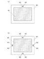
本実施の形態では、光センサを内蔵する表示装置の一形態について説明する。図1は光センサを内蔵する表示装置800を示している。図1(A)は、表示部801の外側上部に光センサ802及び光センサ803が設けられている。図1(B)は表示部801の周囲に光センサ802及び光センサ803が複数設けられている。
(Embodiment 1)
In this embodiment, one embodiment of a display device including a photosensor will be described. FIG. 1 shows a
光センサ802は光電変換素子が非晶質半導体で構成されており、光センサ803は光電変換素子が多結晶半導体で構成されている。光センサ802または光センサ803により表示装置周囲の照度を検出し、表示装置の発光輝度を調整する。例えば、表示装置周囲の照度が強い場合は表示部801の発光輝度を大きくし、表示装置周囲の照度が弱い場合は表示部801の発光輝度を小さくすることで、使用者の体感上の輝度変化を軽減し、消費電力の増加を抑えることができる。
In the
図1(B)に示したように、光センサ802及び光センサ803を複数配置することで、表示装置周囲の照度をより正確に検出することができる。また、例えば幾つかの光センサが隠された場合においても、残りの光センサにより表示装置周囲の照度を検出することができる。
As shown in FIG. 1B, the illuminance around the display device can be detected more accurately by arranging a plurality of the
図2(A)は、光電変換素子に非晶質半導体として非晶質シリコン薄膜を用いた光センサ(以下、非晶質薄膜光センサという)と、光電変換素子に多結晶半導体として多結晶シリコン薄膜を用いた光センサ(以下、多結晶薄膜光センサという)の光感度特性を示す図である。図2(A)中、特性811は非晶質薄膜光センサの光感度特性を示し、特性812が多結晶薄膜光センサの光感度特性を示している。 FIG. 2A shows an optical sensor using an amorphous silicon thin film as an amorphous semiconductor for a photoelectric conversion element (hereinafter referred to as an amorphous thin film optical sensor), and polycrystalline silicon as a polycrystalline semiconductor for a photoelectric conversion element. It is a figure which shows the photosensitivity characteristic of the optical sensor (henceforth a polycrystalline thin film optical sensor) using a thin film. In FIG. 2A, a characteristic 811 indicates the photosensitivity characteristic of the amorphous thin film photosensor, and a characteristic 812 indicates the photosensitivity characteristic of the polycrystalline thin film photosensor.
非晶質薄膜光センサおよび多結晶薄膜光センサとも、波長0.4〜0.8μmの可視光に対して光感度を有している。また、非晶質薄膜光センサは可視光に対しての光感度が大きく、波長0.6μm付近に最大感度を有している。多結晶薄膜光センサは、可視光に対する光感度は非晶質薄膜光センサよりも小さいものの、波長0.7μm付近に最大感度を有しており、また、赤外光の検出も可能である。 Both the amorphous thin film optical sensor and the polycrystalline thin film optical sensor have photosensitivity for visible light having a wavelength of 0.4 to 0.8 μm. The amorphous thin film optical sensor has a high photosensitivity to visible light, and has a maximum sensitivity in the vicinity of a wavelength of 0.6 μm. The polycrystalline thin film optical sensor has a maximum sensitivity in the vicinity of a wavelength of 0.7 μm, and can detect infrared light, though the optical sensitivity to visible light is smaller than that of the amorphous thin film optical sensor.
図2(B)は、入射照度に対する光センサの出力の関係を説明する図である。特性821は非晶質薄膜光センサの入射照度と出力の関係を示しており、特性822は多結晶薄膜光センサの入射照度と出力の関係を示している。非晶質薄膜光センサは可視光に対して光感度が大きいため、比較的暗い環境下においても正確に照度を測定することができるが、屋外などの照度が強いところでは出力が飽和してしまい、正確な照度を測定することができない。一方、多結晶薄膜光センサは、非晶質薄膜光センサよりも可視光に対して光感度が小さいため、入射照度が強くても出力が飽和しにくく、照度を正確に測定することができる。 FIG. 2B is a diagram for explaining the relationship of the output of the optical sensor with respect to the incident illuminance. A characteristic 821 shows the relationship between the incident illuminance and output of the amorphous thin film photosensor, and a characteristic 822 shows the relationship between the incident illuminance and output of the polycrystalline thin film photosensor. Amorphous thin-film photosensors have high photosensitivity to visible light, so they can accurately measure illuminance even in a relatively dark environment, but the output saturates at high illuminance such as outdoors. Unable to measure the exact illuminance. On the other hand, since the polycrystalline thin film optical sensor has lower photosensitivity to visible light than the amorphous thin film optical sensor, the output is not easily saturated even when the incident illuminance is strong, and the illuminance can be measured accurately.
可視光に対して異なる光感度を持つ光センサを用いることで、表示装置周囲の明るさをより正確に検出し、表示装置の輝度を最適な状態とすることができる。 By using an optical sensor having different photosensitivity to visible light, the brightness around the display device can be detected more accurately, and the brightness of the display device can be optimized.
図3は、本実施の形態を適用した表示装置のブロック図である。中央制御部831は入出力ポート、メモリなどを有している。外部入力833は、外部からの映像信号の入り口であり、各種映像信号は外部入力833を通じて中央制御部831に入力される。使用者は操作部834において、輝度や色調などを別途設定することができる。光センサ841及び光センサ842は、可視光の検出感度が異なる光センサであり、例えば、光センサ841として非晶質薄膜光センサを用い、光センサ842として多結晶薄膜光センサを用いる。 FIG. 3 is a block diagram of a display device to which this embodiment is applied. The central control unit 831 has an input / output port, a memory, and the like. The external input 833 is an entrance of an external video signal, and various video signals are input to the central control unit 831 through the external input 833. The user can set brightness, color tone, and the like separately on the operation unit 834. The optical sensor 841 and the optical sensor 842 are optical sensors having different detection sensitivity of visible light. For example, an amorphous thin film optical sensor is used as the optical sensor 841, and a polycrystalline thin film optical sensor is used as the optical sensor 842.
中央制御部831は、操作部834で設定された輝度や色調などを基に、光センサ841及び光センサ842により検出された表示装置周囲の照度を考慮して、外部入力833から入力された映像信号を変換し、表示部832に映像を表示する。 The central control unit 831 considers the illuminance around the display device detected by the optical sensor 841 and the optical sensor 842 based on the luminance and color tone set by the operation unit 834, and the video input from the external input 833. The signal is converted and an image is displayed on the display unit 832.
中央制御部831は、光センサ841及び光センサ842の双方の信号出力を比較し、通常は信号強度の強い光センサ841(非晶質薄膜光センサ)の出力をもとに表示部832に表示する映像の輝度補正を行う。ただし、信号強度が強くても、信号出力が飽和している場合は、光センサ842(多結晶薄膜光センサ)の信号出力をもとに表示部832に表示する映像の輝度補正を行う。このようにして、光センサ841と光センサ842を使い分けることで、表示装置周囲の照度変化が大きくても適切に輝度補正を行うことができる。 The central control unit 831 compares the signal outputs of both the optical sensor 841 and the optical sensor 842, and normally displays the signal on the display unit 832 based on the output of the optical sensor 841 (amorphous thin film optical sensor) having a high signal intensity. Correct the brightness of the video to be played. However, even if the signal intensity is strong, if the signal output is saturated, the luminance of the video displayed on the display unit 832 is corrected based on the signal output of the optical sensor 842 (polycrystalline thin film optical sensor). In this way, by properly using the optical sensor 841 and the optical sensor 842, it is possible to appropriately perform luminance correction even if the illuminance change around the display device is large.
また、図2(A)で示した通り、非晶質薄膜光センサである光センサ841は赤外光を検出しないが、多結晶薄膜光センサである光センサ842は赤外光も検出する。この特性差を利用し、中央制御部831に予め記憶させた算出方法を用いて双方の出力差を検出することで、表示装置周囲の赤外光の照度を検出することができる。 As shown in FIG. 2A, the optical sensor 841 that is an amorphous thin film optical sensor does not detect infrared light, but the optical sensor 842 that is a polycrystalline thin film optical sensor also detects infrared light. By utilizing this characteristic difference and detecting the output difference between the two using a calculation method stored in the central control unit 831 in advance, the illuminance of infrared light around the display device can be detected.
例えば、通常は室内よりも屋外の方が赤外光の照度が強いため、赤外光の照度が強い場合は、可視光の照度を基にした輝度補正のみでなく、屋外使用を前提とした色調補正を同時に行うことで、表示品質を改善することができる。 For example, since infrared illumination is usually stronger outdoors than indoors, if the illumination intensity of infrared light is strong, not only brightness correction based on the illumination intensity of visible light but also the assumption of outdoor use Display quality can be improved by performing color tone correction simultaneously.
非晶質薄膜光センサは、例えば非晶質シリコン膜を用いたpin型のフォトダイオードを用いることができる。まず、第1の半導体層としてp型の導電型を有する半導体層を形成し、次に第2の半導体層として高抵抗な半導体層(i型半導体層)を形成し、次に第3の半導体層としてn型の導電型を有する半導体層を形成する。 As the amorphous thin film optical sensor, for example, a pin type photodiode using an amorphous silicon film can be used. First, a semiconductor layer having p-type conductivity is formed as the first semiconductor layer, then a high-resistance semiconductor layer (i-type semiconductor layer) is formed as the second semiconductor layer, and then the third semiconductor A semiconductor layer having n-type conductivity is formed as the layer.
第1の半導体層はp型半導体層であり、p型を付与する不純物元素を含む非晶質シリコン膜により形成することができる。第1の半導体層は、13族の不純物元素(例えばボロン(B))を含む半導体材料ガスを用いて、プラズマCVD法により形成する。半導体材料ガスとしてはシラン(SiH4)を用いればよい。または、Si2H6、SiH2Cl2、SiHCl3、SiCl4、SiF4等を用いてもよい。また、不純物元素を含まない非晶質シリコン膜を形成した後に、拡散法やイオン注入法を用いて該非晶質シリコン膜に不純物元素を導入してもよい。イオン注入法等により不純物元素を導入した後に加熱等を行うことで、不純物元素を拡散させるとよい。この場合に非晶質シリコン膜を形成する方法としては、LPCVD法、気相成長法、又はスパッタリング法等を用いればよい。第1の半導体層の膜厚は10nm以上50nm以下となるよう形成することが好ましい。 The first semiconductor layer is a p-type semiconductor layer and can be formed using an amorphous silicon film containing an impurity element imparting p-type conductivity. The first semiconductor layer is formed by a plasma CVD method using a semiconductor material gas containing a Group 13 impurity element (eg, boron (B)). Silane (SiH 4 ) may be used as the semiconductor material gas. Alternatively, Si 2 H 6 , SiH 2 Cl 2 , SiHCl 3 , SiCl 4 , SiF 4, or the like may be used. Alternatively, after an amorphous silicon film not containing an impurity element is formed, the impurity element may be introduced into the amorphous silicon film by a diffusion method or an ion implantation method. It is preferable to diffuse the impurity element by introducing an impurity element by an ion implantation method or the like and then performing heating or the like. In this case, as a method for forming the amorphous silicon film, an LPCVD method, a vapor phase growth method, a sputtering method, or the like may be used. The first semiconductor layer is preferably formed to have a thickness of 10 nm to 50 nm.
第2の半導体層は、i型半導体層(真性半導体層)であり、非晶質シリコン膜により形成する。第2の半導体層は、半導体材料ガスを用いて、非晶質シリコン膜をプラズマCVD法により形成する。半導体材料ガスとしては、シラン(SiH4)を用いればよい。または、Si2H6、SiH2Cl2、SiHCl3、SiCl4、SiF4等を用いてもよい。第2の半導体層の形成は、LPCVD法、気相成長法、スパッタリング法等により行っても良い。第2の半導体層の膜厚は200nm以上1000nm以下となるように形成することが好ましい。 The second semiconductor layer is an i-type semiconductor layer (intrinsic semiconductor layer) and is formed using an amorphous silicon film. As the second semiconductor layer, an amorphous silicon film is formed by a plasma CVD method using a semiconductor material gas. Silane (SiH 4 ) may be used as the semiconductor material gas. Alternatively, Si 2 H 6 , SiH 2 Cl 2 , SiHCl 3 , SiCl 4 , SiF 4, or the like may be used. The second semiconductor layer may be formed by LPCVD, vapor deposition, sputtering, or the like. The second semiconductor layer is preferably formed so as to have a thickness of 200 nm to 1000 nm.
第3の半導体層は、n型半導体層であり、n型を付与する不純物元素を含む非晶質シリコン膜により形成する。第3の半導体層は、15族の不純物元素(例えばリン(P))を含む半導体材料ガスを用いて、プラズマCVD法により形成する。半導体材料ガスとしてはシラン(SiH4)を用いればよい。または、Si2H6、SiH2Cl2、SiHCl3、SiCl4、SiF4等を用いてもよい。また、不純物元素を含まない非晶質シリコン膜を形成した後に、拡散法やイオン注入法を用いて該非晶質シリコン膜に不純物元素を導入してもよい。イオン注入法等により不純物元素を導入した後に加熱等を行うことで、不純物元素を拡散させるとよい。この場合に非晶質シリコン膜を形成する方法としては、LPCVD法、気相成長法、又はスパッタリング法等を用いればよい。第3の半導体層の膜厚は20nm以上200nm以下となるよう形成することが好ましい。 The third semiconductor layer is an n-type semiconductor layer and is formed using an amorphous silicon film containing an impurity element imparting n-type conductivity. The third semiconductor layer is formed by a plasma CVD method using a semiconductor material gas containing a Group 15 impurity element (for example, phosphorus (P)). Silane (SiH 4 ) may be used as the semiconductor material gas. Alternatively, Si 2 H 6 , SiH 2 Cl 2 , SiHCl 3 , SiCl 4 , SiF 4, or the like may be used. Alternatively, after an amorphous silicon film not containing an impurity element is formed, the impurity element may be introduced into the amorphous silicon film by a diffusion method or an ion implantation method. It is preferable to diffuse the impurity element by introducing an impurity element by an ion implantation method or the like and then performing heating or the like. In this case, as a method for forming the amorphous silicon film, an LPCVD method, a vapor phase growth method, a sputtering method, or the like may be used. The third semiconductor layer is preferably formed so as to have a thickness of 20 nm to 200 nm.
また、第1の半導体層、第2の半導体層、及び第3の半導体層として、非晶質半導体ではなく多結晶半導体もしくは微結晶半導体を用いることで、多結晶薄膜光センサを形成することができる。また、第2の半導体層のみを多結晶半導体もしくは微結晶半導体で形成してもよい。 In addition, a polycrystalline thin film optical sensor can be formed by using a polycrystalline semiconductor or a microcrystalline semiconductor instead of an amorphous semiconductor as the first semiconductor layer, the second semiconductor layer, and the third semiconductor layer. it can. Further, only the second semiconductor layer may be formed using a polycrystalline semiconductor or a microcrystalline semiconductor.
微結晶半導体は、ギブスの自由エネルギーを考慮すれば非晶質と単結晶の中間的な準安定状態に属するものである。すなわち、自由エネルギー的に安定な第3の状態を有する半導体であって、短距離秩序を持ち格子歪みを有する。柱状または針状結晶が基板表面に対して法線方向に成長している。微結晶半導体の代表例である微結晶シリコンは、そのラマンスペクトルが単結晶シリコンを示す520cm−1よりも低波数側に、シフトしている。即ち、単結晶シリコンを示す520cm−1と非晶質シリコンを示す480cm−1の間に微結晶シリコンのラマンスペクトルのピークがある。また、未結合手(ダングリングボンド)を終端するため水素またはハロゲンを少なくとも1原子%またはそれ以上含ませている。さらに、ヘリウム、アルゴン、クリプトン、ネオンなどの希ガス元素を含ませて格子歪みをさらに助長させることで、安定性が増し良好な微結晶半導体膜が得られる。 A microcrystalline semiconductor belongs to a metastable state between an amorphous state and a single crystal state in consideration of Gibbs free energy. That is, it is a semiconductor having a third state that is stable in terms of free energy, and has a short-range order and lattice distortion. Columnar or needle-like crystals grow in the normal direction with respect to the substrate surface. Microcrystalline silicon which is a typical example of a microcrystalline semiconductor has a Raman spectrum shifted to a lower wave number side than 520 cm −1 indicating single crystal silicon. That is, the peak of the Raman spectrum of microcrystalline silicon is between 520 cm −1 indicating single crystal silicon and 480 cm −1 indicating amorphous silicon. In addition, at least 1 atomic% or more of hydrogen or halogen is contained to terminate dangling bonds (dangling bonds). Further, by adding a rare gas element such as helium, argon, krypton, or neon to further promote lattice distortion, stability can be improved and a good microcrystalline semiconductor film can be obtained.
この微結晶半導体膜は、周波数が数十MHz〜数百MHzの高周波プラズマCVD法、または周波数が1GHz以上のマイクロ波プラズマCVD装置により形成することができる。代表的には、SiH4、Si2H6、SiH2Cl2、SiHCl3、SiCl4、SiF4などの水素化珪素を水素で希釈して形成することができる。また、水素化珪素及び水素に加え、ヘリウム、アルゴン、クリプトン、ネオンから選ばれた一種または複数種の希ガス元素で希釈して微結晶半導体膜を形成することができる。これらのときの水素化珪素に対して水素の流量比を5倍以上200倍以下、好ましくは50倍以上150倍以下、更に好ましくは100倍とする。さらには、シリコンを含む気体中に、CH4、C2H6等の炭化物気体、GeH4、GeF4等のゲルマニウム化気体、F2等を混入させてもよい。 This microcrystalline semiconductor film can be formed by a high-frequency plasma CVD method with a frequency of several tens to several hundreds of MHz or a microwave plasma CVD apparatus with a frequency of 1 GHz or more. Typically, silicon hydride such as SiH 4 , Si 2 H 6 , SiH 2 Cl 2 , SiHCl 3 , SiCl 4 , and SiF 4 can be formed by diluting with hydrogen. In addition to silicon hydride and hydrogen, the microcrystalline semiconductor film can be formed by dilution with one or more kinds of rare gas elements selected from helium, argon, krypton, and neon. The flow rate ratio of hydrogen to silicon hydride at these times is 5 to 200 times, preferably 50 to 150 times, and more preferably 100 times. Furthermore, carbide gas such as CH 4 and C 2 H 6 , germanium gas such as GeH 4 and GeF 4 , F 2 and the like may be mixed in a gas containing silicon.
また、光電効果で発生した正孔の移動度は電子の移動度に比べて小さいため、半導体層を積層して形成するpin型フォトダイオードの場合は、p型の半導体層側を受光面とするとよい。 In addition, since the mobility of holes generated by the photoelectric effect is smaller than the mobility of electrons, in the case of a pin-type photodiode formed by stacking semiconductor layers, the p-type semiconductor layer side is the light receiving surface. Good.
このようにして、可視光に対して異なる光感度を持つ非晶質薄膜光センサと多結晶薄膜光センサを用いることで、周囲の照度を正確に検出し、表示装置の発光輝度を最適な状態とすることで、使用者の体感上の輝度変化を軽減し、消費電力の増加を抑えることができる。また、非晶質薄膜光センサと多結晶薄膜光センサの出力差により赤外光の照度を検出し、表示部の色調補正を行うことで、表示品質を改善することができる。 In this way, by using an amorphous thin-film photosensor and a polycrystalline thin-film photosensor with different photosensitivity to visible light, the ambient illuminance can be accurately detected and the light emission luminance of the display device can be optimized. By doing so, it is possible to reduce the luminance change in the user's experience and suppress the increase in power consumption. Further, the display quality can be improved by detecting the illuminance of infrared light based on the output difference between the amorphous thin film optical sensor and the polycrystalline thin film optical sensor and correcting the color tone of the display unit.
(実施の形態2)
本実施の形態では、光センサを内蔵する表示装置の実施の形態1とは異なる形態について説明する。
(Embodiment 2)
In this embodiment mode, a mode different from that of
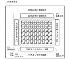
表示装置の一例として、本実施の形態では液晶表示装置を例として図4を参照して説明する。表示装置220は、画素回路221、表示素子制御回路222及び光センサ制御回路223を有する。画素回路221は、マトリクス状に配置された複数の画素224を有する。各々の画素224は、表示素子225と光センサ226もしくは光センサ236を有する。
In this embodiment, a liquid crystal display device is described as an example of the display device with reference to FIG. The display device 220 includes a
光センサ226は、実施の形態1で説明した非晶質薄膜光センサであり、光センサ236は多結晶薄膜光センサである。図4では、光センサ226を有する画素と、光センサ236を有する画素が一列ずつ交互に配置する例が示されているが、特にこれに限定されない。例えば、すべての画素に光センサ226もしくは光センサ236が配置されていなくてもよく、一画素おきまたは数画素おきに配置されていてもよい。
The
表示素子225は、トランジスタ、保持容量、液晶層を有する液晶素子などを有する。トランジスタは、保持容量への電荷の注入もしくは排出を制御する機能を有する。保持容量は、液晶層に印加する電圧に相当する電荷を保持する機能を有する。液晶層に電圧を印加することで偏光方向が変化する現象を利用して、液晶層を透過する光の明暗(階調)を作り、画像表示が実現される。液晶表示装置には、光源(バックライト)を液晶層の後面側に設け、光源から液晶層を透過してきた光で画像を表示する透過型液晶表示装置と、外光もしくは液晶層の前面側に設けた光源(フロントライト)の光を反射させて画像を表示する反射型液晶表示装置がある。
The
なお、カラー画像表示を行う方式として、カラーフィルタを用いる方式、所謂、カラーフィルタ方式がある。これは、液晶層を透過した光がカラーフィルタを通過することで、特定の色(例えば、赤(R)、緑(G)、青(B))の階調を作ることができる。ここで、カラーフィルタ方式を用いる際に、赤(R)、緑(G)、青(B)のいずれかの色を発光する機能を有する画素224を、各々、R画素、G画素、B画素と呼ぶことにする。なお、白黒画像表示のみを行う場合は、カラーフィルタを用いなくてもよい。
As a method for displaying a color image, there is a so-called color filter method using a color filter. This is because the light transmitted through the liquid crystal layer passes through the color filter, so that gradations of specific colors (for example, red (R), green (G), and blue (B)) can be created. Here, when the color filter method is used, a
また、カラー画像表示を行う別の方式として、バックライトを特定の色(例えば、赤(R)、緑(G)、青(B))の光源で構成して各色を順次点灯する方式、所謂、フィールドシーケンシャル方式がある。フィールドシーケンシャル方式では、各色の光源が点灯している期間に、液晶層を透過する光の明暗を作ることで、当該色の諧調を作ることができる。 As another method for displaying a color image, a backlight is composed of light sources of specific colors (for example, red (R), green (G), and blue (B)), and each color is sequentially turned on, so-called. There is a field sequential method. In the field sequential method, the tone of the color can be made by making light and darkness of the light transmitted through the liquid crystal layer during the period when the light source of each color is turned on.
なお、表示素子225が液晶素子を有する場合について説明したが、発光素子などの他の素子を有していてもよい。発光素子は、電流または電圧によって輝度が制御される素子であり、具体的には発光ダイオード、EL素子(有機EL素子(Organic Light Emitting Diode:OLED)、無機EL素子)などが挙げられる。
Note that although the case where the
本実施の形態で示す光センサ226及び光センサ236は、フォトダイオードなど、受光することで電気信号を発する機能を有する素子(光電変換素子)と、トランジスタとを有する。
The
表示素子制御回路222は、表示素子225を制御するための回路であり、ビデオデータ信号線などの信号線(「ソース信号線」ともいう)を介して表示素子225に信号を入力する表示素子駆動回路227と、走査線(「ゲート信号線」ともいう)を介して表示素子225に信号を入力する表示素子駆動回路228を有する。例えば、表示素子駆動回路228は、特定の行に配置された画素が有する表示素子225を選択する機能を有する。また、表示素子駆動回路227は、選択された行の画素が有する表示素子225に任意の電位を与える機能を有する。なお、表示素子駆動回路228により高電位を印加された表示素子では、トランジスタが導通状態となり、表示素子駆動回路227により与えられる電位が供給される。
The display element control circuit 222 is a circuit for controlling the
光センサ制御回路223は、光センサ226を制御するための回路であり、光センサ出力信号線、光センサ基準信号線などの光センサ読み出し回路229と、光センサ駆動回路230を有する。光センサ駆動回路230は、特定の行に配置された画素が有する光センサ226に対して、後述するリセット動作と選択動作とを行う機能を有する。また、光センサ読み出し回路229は、選択された行の画素が有する光センサ226の出力信号を取り出す機能を有する。なお、光センサ読み出し回路229は、アナログ信号である光センサの出力を、OPアンプを用いてアナログ信号のまま表示装置外部に取り出す構成や、A/D変換回路を用いてデジタル信号に変換してから表示装置外部に取り出す構成としてもよい。
The optical sensor control circuit 223 is a circuit for controlling the
光センサを含む表示装置220において、酸化物半導体を用いたトランジスタを有する回路を設ける構成とする。 In the display device 220 including an optical sensor, a circuit including a transistor including an oxide semiconductor is provided.
光センサを含む表示装置220に含まれる酸化物半導体層を用いるトランジスタは、その電気的特性変動を抑止するため、変動要因となる水素、水分、水酸基又は水素化物(水素化合物ともいう)などの不純物を酸化物半導体層より意図的に排除し、かつ不純物の排除工程によって同時に減少してしまう酸化物半導体を構成する主成分材料である酸素を供給することによって、酸化物半導体層を高純度化及び電気的にi型(真性)化する。 A transistor using an oxide semiconductor layer included in the display device 220 including an optical sensor has an impurity such as hydrogen, moisture, a hydroxyl group, or a hydride (also referred to as a hydrogen compound) that causes variation in order to suppress variation in electrical characteristics of the transistor. By supplying oxygen, which is a main component material of the oxide semiconductor, which is intentionally excluded from the oxide semiconductor layer and simultaneously reduced by the impurity removal step, the oxide semiconductor layer is highly purified and It becomes i-type (intrinsic) electrically.
よって酸化物半導体中の水素及びキャリアは少なければ少ないほどよく、本明細書に開示するトランジスタは、酸化物半導体に含まれる水素が5×10¹⁹/cm3以下、好ましくは5×1018/cm3以下、より好ましくは5×1017/cm3以下か、または1×1016/cm3未満として、酸化物半導体に含まれる水素をゼロに近いほど極力除去し、キャリア密度を1×1014/cm3未満、好ましくは1×1012/cm3未満、さらに好ましくは1×1011/cm3未満とした酸化物半導体でチャネル形成領域が形成されるトランジスタである。 Therefore, the fewer hydrogen and carriers in the oxide semiconductor are, the better. The transistor disclosed in this specification has hydrogen of 5 × 10 19 / cm 3 or less, preferably 5 × 10 18 / cm 3 in the oxide semiconductor. 3 or less, more preferably 5 × 10 17 / cm 3 or less, or less than 1 × 10 16 / cm 3 , hydrogen contained in the oxide semiconductor is removed as close to zero as possible, and the carrier density is 1 × 10 14. A transistor in which a channel formation region is formed using an oxide semiconductor of less than / cm 3 , preferably less than 1 × 10 12 / cm 3 , more preferably less than 1 × 10 11 / cm 3 .
酸化物半導体を用いたトランジスタは、酸化物半導体中にキャリアが極めて少ない(ゼロに近い)ため、トランジスタのオフ電流を少なくすることができる。トランジスタのオフ電流は少なければ少ないほど好ましい。オフ電流とは、−1V〜−10Vの間のいずれかのゲート電圧を印加した場合のトランジスタのソース、ドレイン間を流れる電流のことであり、本明細書に開示する酸化物半導体を用いたトランジスタは、チャネル幅(W)1μmあたりの電流値が10aA/μm以下、好ましくは1aA/μm以下、さらに好ましくは1zA/μm以下である。さらに、pn接合がなく、ホットキャリア劣化がないため、トランジスタの電気的特性がこれらの影響を受けない。 A transistor using an oxide semiconductor has very few carriers (close to zero) in the oxide semiconductor, so that off-state current of the transistor can be reduced. The smaller the off-state current of the transistor, the better. The off-state current is a current that flows between the source and the drain of a transistor when any gate voltage between −1 V and −10 V is applied. The transistor using an oxide semiconductor disclosed in this specification The current value per channel width (W) of 1 μm is 10 aA / μm or less, preferably 1 aA / μm or less, and more preferably 1 zA / μm or less. Further, since there is no pn junction and there is no hot carrier deterioration, the electrical characteristics of the transistor are not affected by these effects.
画素224の回路図の一例について、図5を用いて説明する。画素224は、トランジスタ201、保持容量202及び液晶素子203を有する表示素子225と、フォトダイオード204、トランジスタ205及びトランジスタ206を有する光センサ226もしくは光センサ236とを有する。
An example of a circuit diagram of the
トランジスタ201は、ゲートがゲート信号線207に、ソース又はドレインの一方がビデオデータ信号線210に、ソース又はドレインの他方が保持容量202の一方の電極と液晶素子203の一方の電極に電気的に接続されている。保持容量202の他方の電極と液晶素子203の他方の電極は一定の電位に保たれている。液晶素子203は、一対の電極と、該一対の電極の間に液晶層を含む素子である。
In the
トランジスタ201は、ゲート信号線207に”H”が印加されると、ビデオデータ信号線210の電位を保持容量202と液晶素子203に供給する。保持容量202は、供給された電位を保持する。液晶素子203は、供給された電位により、光の透過率を変更する。
When “H” is applied to the
酸化物半導体を用いたトランジスタであるトランジスタ201、205、206は、オフ電流が非常に小さいため、保持容量は非常に小さくてよく、また設けなくてもよい。
The
フォトダイオード204は、非晶質半導体、または多結晶半導体、または微結晶半導体で形成され、一方の電極がフォトダイオードリセット信号線208に、他方の電極がゲート信号線213を介してトランジスタ205のゲートに電気的に接続されている。トランジスタ205は、ソース又はドレインの一方が光センサ基準信号線212に、ソース又はドレインの他方がトランジスタ206のソース又はドレインの一方に電気的に接続されている。トランジスタ206は、ゲートがゲート信号線209に、ソース又はドレインの他方が光センサ出力信号線211に電気的に接続されている。
The
なお、トランジスタ205とトランジスタ206の配置は、図5の構成に限定されない。例えば、トランジスタ206のソース又はドレインの一方が光センサ基準信号線212に、他方がトランジスタ205のソース又はドレインの一方に電気的に接続され、トランジスタ205のゲートがゲート信号線209に、ソース又はドレインの他方が光センサ出力信号線211に電気的に接続される構成としてもよい。
Note that the arrangement of the
次に、光センサ読み出し回路229の構成の一例について、図6を用いて説明する。図6において、光センサ読み出し回路229が有する画素1列に対応する光センサ駆動回路230は、トランジスタ231と保持容量232を有する。また、211は当該画素1列に対応する光センサ出力信号線、233はプリチャージ信号線である。
Next, an example of the configuration of the optical sensor readout circuit 229 will be described with reference to FIG. In FIG. 6, the
図5において、トランジスタ205、トランジスタ206、図6においてトランジスタ231は酸化物半導体層を用いるトランジスタである。
5A and 5B, the
図4に示した光センサ読み出し回路229が有する画素1列に対応する光センサ駆動回路230では、画素内における光センサの動作に先立ち、光センサ出力信号線211の電位を基準電位に設定する。光センサ出力信号線211に設定する基準電位は高電位でも低電位でもよい。図6では、プリチャージ信号線233を”H”とすることで、光センサ出力信号線211を基準電位である高電位に設定することができる。なお、保持容量232は、光センサ出力信号線211の寄生容量が大きい場合には、特別に設けなくても良い。
In the
次に、表示装置における光センサの読み出し動作の一例について、図7のタイミングチャートを用いて説明する。図7において、信号251〜信号254は、図5におけるフォトダイオードリセット信号線208、トランジスタ206のゲートが接続されたゲート信号線209、トランジスタ205のゲートが接続されたゲート信号線213、光センサ出力信号線211の電位に相当する。また、信号255は、図6におけるプリチャージ信号線233の電位に相当する。
Next, an example of a reading operation of the optical sensor in the display device will be described with reference to a timing chart in FIG. 7, the
時刻Aにおいて、フォトダイオードリセット信号線208の電位(信号251)を”H”とする(リセット動作)と、フォトダイオード204が導通し、トランジスタ205のゲートが接続されたゲート信号線213の電位(信号253)が”H”となる。また、プリチャージ信号線233の電位(信号255)を”H”とすると、光センサ出力信号線211の電位(信号254)は”H”にプリチャージされる。
At time A, when the potential of the photodiode reset signal line 208 (signal 251) is set to “H” (reset operation), the
時刻Bにおいて、フォトダイオードリセット信号線208の電位(信号251)を”L”にする(累積動作)と、フォトダイオード204の光電流により、トランジスタ205のゲートが接続されたゲート信号線213の電位(信号253)が低下し始める。フォトダイオード204は、光が照射されると光電流が増大するので、照射される光の量に応じてトランジスタ205のゲートが接続されたゲート信号線213の電位(信号253)は変化する。すなわち、トランジスタ205のソースとドレイン間の電流が変化する。
At time B, when the potential of the photodiode reset signal line 208 (signal 251) is set to “L” (accumulation operation), the potential of the
時刻Cにおいて、ゲート信号線209の電位(信号252)を”H”にする(選択動作)と、トランジスタ206が導通し、光センサ基準信号線212と光センサ出力信号線211とが、トランジスタ205とトランジスタ206とを介して導通する。すると、光センサ出力信号線211の電位(信号254)は、低下していく。なお、時刻C以前に、プリチャージ信号線233の電位(信号255)を”L”とし、光センサ出力信号線211のプリチャージを終了しておく。ここで、光センサ出力信号線211の電位(信号254)が特定の電位に達するまでの時間(電位が変化する速さ)は、トランジスタ205のソースとドレイン間の電流に依存する。すなわち、フォトダイオード204に照射されている光の量に応じて変化する。
At time C, when the potential of the gate signal line 209 (signal 252) is set to “H” (selection operation), the
時刻Dにおいて、ゲート信号線209の電位(信号252)を”L”にすると、トランジスタ206が遮断され、光センサ出力信号線211の電位(信号254)は、時刻D以後、一定値となる。ここで、一定値となる電位は、フォトダイオード204に照射されている光の量に応じて変化する。したがって、光センサ出力信号線211の電位を取得することで、フォトダイオード204に照射されている光の量を知ることができる。
At time D, when the potential of the gate signal line 209 (signal 252) is set to “L”, the
上記のように、個々の光センサの動作は、リセット動作、累積動作、選択動作を繰り返すことで実現される。表示装置において高速撮像を実現するためには、全画素のリセット動作、累積動作、選択動作を高速に実行することが必要である。また、図5におけるトランジスタ206のオフリーク電流が大きいと、トランジスタ205を介して、光センサ出力信号線211から、光センサ基準信号線212へリーク電流が流れてしまう。すると、リセット動作中にトランジスタ205のゲート電圧が所望の電圧に達しない、光センサ出力信号線211及び光センサ基準信号線212の電位が不安定になる、などの光センサ動作の不具合が生じる恐れがある。
As described above, the operation of each optical sensor is realized by repeating the reset operation, the accumulation operation, and the selection operation. In order to realize high-speed imaging in a display device, it is necessary to perform reset operation, accumulation operation, and selection operation for all pixels at high speed. In addition, when the off-leakage current of the
しかし、本明細書に開示する発明においては、トランジスタ206を、酸化物半導体を用いたトランジスタで形成しており、オフ電流が非常に小さいので上記不具合を低減することができる。
However, in the invention disclosed in this specification, the
本実施の形態では、光センサを表示部外ではなく表示部内に設けることで、より正確に輝度や色調の補正が可能となる。また、光センサを表示部内に設けることで、光センサが隠される可能性が極めて低くなる。 In this embodiment, by providing the optical sensor inside the display unit instead of outside the display unit, it is possible to correct luminance and color tone more accurately. Further, by providing the optical sensor in the display unit, the possibility that the optical sensor is hidden becomes extremely low.
また、画素内の光センサ上にカラーフィルタを設けることで、表示装置周囲の照度をRGBの各色成分に分光して検出することができる。表示装置周囲の照度をRGBに分光して検出することで、表示装置周囲の色温度や色度分布をより正確に検出し、表示映像の緻密な色調補正を実現することができる。 In addition, by providing a color filter on the photosensor in the pixel, the illuminance around the display device can be detected by spectrally separating each color component of RGB. By detecting the illuminance around the display device by separating it into RGB, the color temperature and chromaticity distribution around the display device can be detected more accurately, and precise color correction of the display image can be realized.
(実施の形態3)
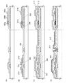
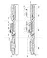
本実施の形態は、実施の形態1及び実施の形態2で説明したトランジスタ及び光センサの作製工程の一例を、図8乃至図11の断面図を参照して説明する。図10(B)に示すトランジスタ390はボトムゲート構造の一種であり、逆スタガ型トランジスタもしくはチャネルエッチ型トランジスタともいう。光センサ391は非晶質薄膜光センサであり、非晶質シリコンで形成したp層、i層、及びn層を積層したpin型のフォトダイオードを有している。光センサ392は多結晶薄膜光センサであり、光電変換素子として一つの多結晶シリコンもしくは微結晶シリコン層中に、p層、i層、及びn層を形成したpin型のフォトダイオードを有している。なお、光センサ391及び光センサ392は、基板側から入射する光ではなく、絶縁層312側から入射する外光350を検出することを前提としている。
(Embodiment 3)
In this embodiment, an example of a manufacturing process of the transistor and the optical sensor described in
なお、本実施の形態で示す光センサ391及び光センサ392は、光センサの光電変換素子部分であるフォトダイオードの断面構造を示している。光センサのトランジスタ部分はトランジスタ390と同様に作製することができる。
Note that the
また、トランジスタ390はシングルゲート構造のトランジスタを用いて説明するが、必要に応じて、チャネル形成領域を複数有するマルチゲート構造のトランジスタとして形成することもできる。
Although the
以下、図8乃至図10を用いて、基板300上にトランジスタ390を作製する工程を説明する。
Hereinafter, a process for manufacturing the
まず、絶縁表面を有する基板300上に導電層を形成した後、第1のフォトリソグラフィ工程によりゲート電極層301、配線層302及び配線層303を形成する。形成されたゲート電極層及び配線層の端部がテーパー形状であると、上に積層するゲート絶縁層の被覆性が向上するため好ましい。なお、レジストマスクをインクジェット法で形成してもよい。レジストマスクをインクジェット法で形成するとフォトマスクを使用しないため、製造コストを低減できる。
First, after a conductive layer is formed over the
基板300は、ガラス基板、セラミック基板、石英基板、サファイア基板の他、本作製工程の処理温度に耐えうる程度の耐熱性を有するプラスチック基板等を用いることができる。また、基板に透光性を要しない場合には、ステンレス合金等の金属の基板の表面に絶縁膜を設けたものを用いてもよい。他にも、結晶化ガラスなどを用いることができる。
As the
ガラス基板としては、後の加熱処理の温度が高い場合には、歪み点が730℃以上のものを用いると良い。また、ガラス基板には、例えば、バリウムホウケイ酸ガラス、アルミノホウケイ酸ガラス若しくはアルミノケイ酸ガラス等の無アルカリガラス基板を用いるとよい。なお、酸化ホウ素(B2O3)と比較して酸化バリウム(BaO)を多く含ませることで、より実用的な耐熱ガラスが得られる。このため、B2O3よりBaOを多く含むガラス基板を用いることが好ましい。 As the glass substrate, a glass substrate having a strain point of 730 ° C. or higher is preferably used when the temperature of the subsequent heat treatment is high. For the glass substrate, for example, an alkali-free glass substrate such as barium borosilicate glass, aluminoborosilicate glass, or aluminosilicate glass may be used. Note that a more practical heat-resistant glass can be obtained by containing more barium oxide (BaO) than boron oxide (B 2 O 3 ). For this reason, it is preferable to use a glass substrate containing more BaO than B 2 O 3 .
また、基板300として、第3世代(550mm×650mm)、第3.5世代(600mm×720mm、または620mm×750mm)、第4世代(680mm×880mm、または730mm×920mm)、第5世代(1100mm×1300mm)、第6世代(1500mm×1850mm)、第7世代(1870mm×2200mm)、第8世代(2200mm×2400mm)、第9世代(2400mm×2800mm、または2450mm×3050mm)、第10世代(2950mm×3400mm)等のガラス基板を用いることができる。
Further, as the
基板300とゲート絶縁層304との間に、下地絶縁層を設けてもよい。下地絶縁層は、基板300からの不純物元素の拡散を防止する機能があり、窒化シリコン膜、酸化シリコン膜、窒化酸化シリコン膜、又は酸化窒化シリコン膜から選ばれた一又は複数の膜による積層構造により形成することができる。下地絶縁層は、スパッタリング法、CVD法、塗布法、印刷法等を適宜用いて形成することができる。下地絶縁膜の膜中にハロゲン元素、例えばフッ素、塩素等を少量添加し、ナトリウム等の可動イオンの固定化をさせてもよい。下地絶縁膜に含ませるハロゲン元素の濃度は、SIMS(二次イオン質量分析法)を用いた分析により得られる濃度ピークが1×1015cm−3以上1×1020cm−3以下の範囲内とすることが好ましい。
A base insulating layer may be provided between the
また、ゲート電極層301、配線層302及び配線層303(これと同じ層で形成される配線層や電極層を含む)の材料は、モリブデン、チタン、クロム、タンタル、タングステン、アルミニウム、銅、ネオジム、スカンジウム等の金属材料又はこれらを主成分とする合金材料を用いて、単層で又は積層して形成することができる。
The materials of the
例えば、ゲート電極層301、配線層302及び配線層303の2層の積層構造としては、アルミニウム層上にモリブデン層が積層された2層の積層構造、銅層上にモリブデン層を積層した2層構造、銅層上に窒化チタン層若しくは窒化タンタル層を積層した2層構造、窒化チタン層とモリブデン層とを積層した2層構造、又は窒化タングステン層とタングステン層とを積層した2層構造とすることが好ましい。3層の積層構造としては、タングステン層または窒化タングステン層と、アルミニウムとシリコンの合金層またはアルミニウムとチタンの合金層と、窒化チタン層またはチタン層とを積層した積層とすることが好ましい。
For example, the two-layer structure of the
次いで、ゲート電極層301、配線層302及び配線層303上にゲート絶縁層304を形成する。
Next, a
ゲート絶縁層304は、プラズマCVD法又はスパッタリング法等を用いて、酸化シリコン層、窒化シリコン層、酸化窒化シリコン層、窒化酸化シリコン層、酸化アルミニウム層、窒化アルミニウム層、酸化窒化アルミニウム層、窒化酸化アルミニウム層、又は酸化ハフニウム層を単層で又は積層して形成することができる。スパッタリング法により酸化シリコン膜を成膜する場合には、ターゲットとしてシリコンターゲット又は石英ターゲットを用い、スパッタガスとして酸素又は、酸素及びアルゴンの混合ガスを用いる。
The
なお、後に形成する高純度化された酸化物半導体(不純物を除去することによりi型化又は実質的にi型化された酸化物半導体)は、界面準位、界面電荷に対して極めて敏感となるため、高純度化された酸化物半導体とゲート絶縁層(GI)の界面特性は特に重要である。そのため高純度化された酸化物半導体に接するゲート絶縁層は、高品質化が要求される。 Note that a highly purified oxide semiconductor (an oxide semiconductor that is i-type or substantially i-type by removing impurities) to be formed later is extremely sensitive to interface states and interface charges. Therefore, the interface characteristics between the highly purified oxide semiconductor and the gate insulating layer (GI) are particularly important. Therefore, the gate insulating layer in contact with the highly purified oxide semiconductor is required to have high quality.
例えば、μ波(2.45GHz)を用いた高密度プラズマCVD法は、緻密で絶縁耐圧の高い高品質な絶縁層を形成できるので好ましい。高純度化された酸化物半導体と高品質ゲート絶縁層とが密接することにより、界面準位を低減して界面特性を良好なものとすることができるからである。 For example, a high-density plasma CVD method using μ waves (2.45 GHz) is preferable because a high-quality insulating layer having a high density and a high withstand voltage can be formed. This is because when the highly purified oxide semiconductor and the high-quality gate insulating layer are in close contact with each other, the interface state can be reduced and interface characteristics can be improved.
もちろん、ゲート絶縁層として良質な絶縁層を形成できるものであれば、スパッタリング法やプラズマCVD法など他の成膜方法を適用することができる。また、成膜後の熱処理によってゲート絶縁層の膜質、酸化物半導体との界面特性が改質される絶縁層であっても良い。いずれにしても、ゲート絶縁層としての膜質が良好であることは勿論のこと、酸化物半導体との界面準位密度を低減し、良好な界面を形成できるものであれば良い。 Needless to say, another film formation method such as a sputtering method or a plasma CVD method can be used as long as a high-quality insulating layer can be formed as the gate insulating layer. Alternatively, an insulating layer in which the film quality of the gate insulating layer and the interface characteristics with the oxide semiconductor are modified by heat treatment after film formation may be used. In any case, any film can be used as long as it can reduce the interface state density with an oxide semiconductor and form a favorable interface as well as the film quality as a gate insulating layer is good.
さらに、トランジスタに対して行う85℃、2×10⁶V/cm、12時間のゲートバイアス・熱ストレス試験(BT試験)においては、酸化物半導体に不純物が含まれていると、不純物と酸化物半導体の主成分との結合手が、強電界(B:バイアス)と高温(T:温度)により切断され、生成された未結合手がしきい値電圧(Vth)のドリフトを誘発することとなる。 Further, in a gate bias / thermal stress test (BT test) performed at 85 ° C. and 2 × 10 6 V / cm for 12 hours for a transistor, if an oxide semiconductor contains impurities, the impurities and oxides A bond with the main component of the semiconductor is cut by a strong electric field (B: bias) and a high temperature (T: temperature), and the generated dangling bond induces a threshold voltage (Vth) drift. .
これに対して、本明細書に開示する発明は、酸化物半導体の不純物、特に水素や水等を極力除去し、上記のようにゲート絶縁層との界面特性を良好にすることにより、BT試験に対しても安定なトランジスタを得ることを可能としている。 In contrast, the invention disclosed in this specification removes impurities of oxide semiconductors, particularly hydrogen and water, as much as possible, and improves the interface characteristics with the gate insulating layer as described above, thereby performing the BT test. This makes it possible to obtain a stable transistor.
ゲート絶縁層304は、ゲート電極層301側から窒化物絶縁層と、酸化物絶縁層との積層構造とすることもできる。例えば、第1のゲート絶縁層としてスパッタリング法により膜厚50nm以上200nm以下の窒化シリコン層(SiNy(y>0))を形成し、第1のゲート絶縁層上に第2のゲート絶縁層として膜厚5nm以上300nm以下の酸化シリコン層(SiOx(x>0))を積層して、膜厚100nmのゲート絶縁層とする。ゲート絶縁層の膜厚は、トランジスタに要求される特性によって適宜設定すればよく350nm乃至400nm程度でもよい。
The
また、ゲート絶縁層304として、ハフニウムシリケート(HfSixOy(x>0、y>0))、窒素が添加されたハフニウムシリケート(HfSixOy(x>0、y>0))、窒素が添加されたハフニウムアルミネート(HfAlxOy(x>0、y>0))、酸化ハフニウム、酸化イットリウムなどのhigh−k材料を用いることでゲートリーク電流を低減できる。さらには、high−k材料と、酸化シリコン、窒化シリコン、酸化窒化シリコン、窒化酸化シリコン、または酸化アルミニウムのいずれか一以上との積層構造とすることができる。
As the
また、ゲート絶縁層304に水素、水酸基及び水分がなるべく含まれないようにするために、成膜の前処理として、スパッタリング装置の予備加熱室でゲート電極層301が形成された基板300、又はゲート絶縁層304までが形成された基板300を予備加熱し、基板300に吸着した水素、水分などの不純物を脱離し排気することが好ましい。なお、予備加熱の温度としては、100℃以上400℃以下好ましくは150℃以上300℃以下である。なお、予備加熱室に設ける排気手段はクライオポンプが好ましい。なお、この予備加熱の処理は省略することもできる。
In order to prevent the
次いで、ゲート絶縁層304上に、スパッタリング法により膜厚2nm以上200nm以下の酸化物半導体層305を形成する(図8(A)参照。)。
Next, the
酸化物半導体層305はスパッタリング法により成膜する。酸化物半導体層305としては、四元系金属酸化物であるIn−Sn−Ga−Zn−O膜や、三元系金属酸化物であるIn−Ga−Zn−O膜、In−Sn−Zn−O膜、In−Al−Zn−O膜、Sn−Ga−Zn−O膜、Al−Ga−Zn−O膜、Sn−Al−Zn−O膜や、二元系金属酸化物であるIn−Zn−O膜、Sn−Zn−O膜、Al−Zn−O膜、Zn−Mg−O膜、Sn−Mg−O膜、In−Mg−O膜、In−Ga−O膜や、In−O膜、Sn−O膜、Zn−O膜などの酸化物半導体層を用いることができる。また、上記酸化物半導体層にSiO2を含んでもよい。
The
酸化物半導体層305をスパッタリング法で作製するためのターゲットとして、酸化亜鉛を主成分とする金属酸化物のターゲットを用いることができる。また、金属酸化物のターゲットの他の例としては、In、Ga、及びZnを含む金属酸化物ターゲット(組成比として、In2O3:Ga2O3:ZnO=1:1:1[mol数比]、In2O3:Ga2O3:ZnO=1:1:2[mol数比])を用いることができる。また、In、Ga、及びZnを含む金属酸化物ターゲットとして、In2O3:Ga2O3:ZnO=2:2:1[mol数比]、またはIn2O3:Ga2O3:ZnO=1:1:4[mol数比]の組成比を有するターゲットを用いることもできる。金属酸化物ターゲットの充填率は90%以上100%以下、好ましくは95%以上99.9%以下である。充填率の高い金属酸化物ターゲットを用いて形成した酸化物半導体層305は緻密な膜となる。
As a target for forming the
本実施の形態では、酸化物半導体層305をIn−Ga−Zn−O系金属酸化物ターゲットを用いてスパッタリング法により成膜する。また、酸化物半導体層305は、希ガス(代表的にはアルゴン)雰囲気下、酸素雰囲気下、又は希ガス(代表的にはアルゴン)及び酸素雰囲気下においてスパッタリング法により形成することができる。
In this embodiment, the
酸化物半導体層の形成は、減圧状態に保持された処理室内に基板を保持し、基板を室温又は400℃未満の温度に加熱する。そして、処理室内の残留水分を除去しつつ水素及び水分が除去されたスパッタガスを導入し、In−Ga−Zn−O系金属酸化物をターゲットとして基板300上に酸化物半導体層305を成膜する。処理室内の残留水分を除去するためには、吸着型の真空ポンプを用いることが好ましい。例えば、クライオポンプ、イオンポンプ、チタンサブリメーションポンプを用いることが好ましい。また、排気手段としては、ターボポンプにコールドトラップを加えたものであってもよい。クライオポンプを用いて排気した成膜室は、例えば、水素原子、水(H2O)など水素原子を含む化合物(より好ましくは炭素原子を含む化合物も)等が排気されるため、当該成膜室で成膜した酸化物半導体膜に含まれる不純物の濃度を低減できる。また、クライオポンプにより処理室内に残留する水分を除去しながらスパッタ成膜を行うことで、酸化物半導体層305を成膜する際の基板温度は室温から400℃未満とすることができる。
In the formation of the oxide semiconductor layer, the substrate is held in a treatment chamber kept under reduced pressure, and the substrate is heated to room temperature or a temperature lower than 400 ° C. Then, a sputtering gas from which hydrogen and moisture are removed is introduced while moisture remaining in the treatment chamber is removed, and the
成膜条件の一例としては、基板とターゲットの間との距離を100mm、圧力0.6Pa、直流(DC)電源電力0.5kW、酸素(酸素流量比率100%)雰囲気下の条件が適用される。なお、パルス直流(DC)電源を用いると、成膜時に発生する粉状物質(パーティクル、ゴミともいう)が軽減でき、膜厚分布も均一となるために好ましい。酸化物半導体膜の膜厚は好ましくは5nm以上30nm以下とする。なお、適用する酸化物半導体材料により適切な厚みは異なり、材料に応じて適宜厚みを選択すればよい。 As an example of the film forming conditions, the distance between the substrate and the target is 100 mm, the pressure is 0.6 Pa, the direct current (DC) power supply power is 0.5 kW, and the oxygen (oxygen flow rate is 100%) atmosphere is applied. . Note that a pulse direct current (DC) power source is preferable because powder substances (also referred to as particles or dust) generated in film formation can be reduced and the film thickness can be uniform. The thickness of the oxide semiconductor film is preferably 5 nm to 30 nm. Note that an appropriate thickness differs depending on an oxide semiconductor material to be used, and the thickness may be selected as appropriate depending on the material.
スパッタリング法にはスパッタ用電源に高周波電源を用いるRFスパッタリング法、直流電源を用いるDCスパッタリング法、さらにパルス的にバイアスを与えるパルスDCスパッタリング法がある。RFスパッタリング法は主に絶縁膜を成膜する場合に用いられ、DCスパッタリング法は主に金属膜を成膜する場合に用いられる。 As the sputtering method, there are an RF sputtering method using a high frequency power source as a sputtering power source, a DC sputtering method using a DC power source, and a pulse DC sputtering method for applying a bias in a pulsed manner. The RF sputtering method is mainly used when an insulating film is formed, and the DC sputtering method is mainly used when a metal film is formed.
また、材料の異なるターゲットを複数設置できる多元スパッタ装置もある。多元スパッタ装置は、同一チャンバーで異なる材料膜を積層成膜することも、同一チャンバーで複数種類の材料を同時に放電させて成膜することもできる。 There is also a multi-source sputtering apparatus in which a plurality of targets of different materials can be installed. The multi-source sputtering apparatus can be formed by stacking different material films in the same chamber, or by simultaneously discharging a plurality of types of materials in the same chamber.
また、チャンバー内部に磁石機構を備えたマグネトロンスパッタリング法を用いるスパッタ装置や、グロー放電を使わずマイクロ波を用いて発生させたプラズマを用いるECRスパッタリング法を用いるスパッタ装置がある。 Further, there are a sputtering apparatus using a magnetron sputtering method having a magnet mechanism inside a chamber, and a sputtering apparatus using an ECR sputtering method using plasma generated using microwaves without using glow discharge.
また、スパッタリング法を用いる成膜方法として、成膜中にターゲット物質とスパッタガス成分とを化学反応させてそれらの化合物薄膜を形成するリアクティブスパッタリング法や、成膜中に基板にも電圧をかけるバイアススパッタリング法もある。 In addition, as a film formation method using a sputtering method, a reactive sputtering method in which a target material and a sputtering gas component are chemically reacted during film formation to form a compound thin film thereof, or a voltage is applied to the substrate during film formation. There is also a bias sputtering method.
酸化物半導体膜を成膜する際に用いるスパッタガスとしては、水素、水、水酸基又は水素化物などの不純物が、濃度ppm程度、濃度ppb程度まで除去された高純度ガスが好ましい。 As a sputtering gas used for forming the oxide semiconductor film, a high-purity gas from which impurities such as hydrogen, water, a hydroxyl group, or hydride are removed to a concentration of about ppm and a concentration of ppb is preferable.
次いで、酸化物半導体層305を第2のフォトリソグラフィ工程により島状の酸化物半導体層306に加工する(図8(B)参照。)。また、島状の酸化物半導体層306を形成するためのレジストマスクをインクジェット法で形成してもよい。レジストマスクをインクジェット法で形成するとフォトマスクを使用しないため、製造コストを低減できる。
Next, the
なお、ここでの酸化物半導体層305のエッチングは、ドライエッチングでもウェットエッチングでもよく、両方を用いてもよい。
Note that the etching of the
ドライエッチングに用いるエッチングガスとしては、塩素を含むガス(塩素系ガス、例えば塩素(Cl2)、三塩化硼素(BCl3)、四塩化珪素(SiCl4)、四塩化炭素(CCl4)など)が好ましい。 As an etching gas used for dry etching, a gas containing chlorine (chlorine-based gas such as chlorine (Cl 2 ), boron trichloride (BCl 3 ), silicon tetrachloride (SiCl 4 ), carbon tetrachloride (CCl 4 ), or the like) Is preferred.
また、フッ素を含むガス(フッ素系ガス、例えば四弗化炭素(CF4)、六弗化硫黄(SF6)、三弗化窒素(NF3)、トリフルオロメタン(CHF3)など)、臭化水素(HBr)、酸素(O2)、これらのガスにヘリウム(He)やアルゴン(Ar)などの希ガスを添加したガス、などを用いることができる。 Gas containing fluorine (fluorine-based gas such as carbon tetrafluoride (CF 4 ), sulfur hexafluoride (SF 6 ), nitrogen trifluoride (NF 3 ), trifluoromethane (CHF 3 ), etc.), bromide Hydrogen (HBr), oxygen (O 2 ), a gas obtained by adding a rare gas such as helium (He) or argon (Ar) to these gases, or the like can be used.
ドライエッチング法としては、平行平板型RIE(Reactive Ion Etching)法や、ICP(Inductively Coupled Plasma:誘導結合型プラズマ)エッチング法を用いることができる。所望の加工形状にエッチングできるように、エッチング条件(コイル型の電極に印加される電力量、基板側の電極に印加される電力量、基板側の電極温度等)を適宜調節する。 As the dry etching method, a parallel plate RIE (Reactive Ion Etching) method or an ICP (Inductively Coupled Plasma) etching method can be used. Etching conditions (such as the amount of power applied to the coil-type electrode, the amount of power applied to the substrate-side electrode, the substrate-side electrode temperature, etc.) are adjusted as appropriate so that the desired processed shape can be etched.
ウェットエッチングに用いるエッチング液としては、燐酸と酢酸と硝酸を混ぜた溶液や、アンモニア過水(31重量%過酸化水素水:28重量%アンモニア水:水=5:2:2容量比)などを用いることができる。また、ITO−07N(関東化学社製)を用いてもよい。 As an etchant used for wet etching, a mixed solution of phosphoric acid, acetic acid, and nitric acid, ammonia perwater (31 wt% hydrogen peroxide water: 28 wt% ammonia water: water = 5: 2: 2 volume ratio), etc. Can be used. Moreover, ITO-07N (manufactured by Kanto Chemical Co., Inc.) may be used.
また、ウェットエッチング後のエッチング液はエッチングされた材料とともに洗浄によって除去される。その除去された材料を含むエッチング液の廃液を精製し、含まれる材料を再利用してもよい。当該エッチング後の廃液から酸化物半導体層に含まれるインジウム等の材料を回収して再利用することにより、資源を有効活用し低コスト化することができる。 In addition, the etchant after the wet etching is removed by cleaning together with the etched material. The waste solution of the etching solution containing the removed material may be purified and the contained material may be reused. By recovering and reusing materials such as indium contained in the oxide semiconductor layer from the waste liquid after the etching, resources can be effectively used and costs can be reduced.
所望の加工形状にエッチングできるように、材料に合わせてエッチング条件(エッチング液、エッチング時間、温度等)を適宜調節する。 Etching conditions (such as an etchant, etching time, and temperature) are adjusted as appropriate depending on the material so that the material can be etched into a desired shape.
次いで、ゲート絶縁層304の上に半導体層307を形成する。半導体層307としては、既知のCVD法、スパッタ法を用いて結晶構造が微結晶または多結晶である半導体層を形成することができる。CVD法で形成する場合の堆積性気体としては、シリコンまたはゲルマニウムを含むガスを用いることができる。シリコンを含む堆積性気体としては、シラン(SiH4)、ジシラン(Si2H6)、ジクロロシラン(SiH2C12)、SiHCl3、塩化珪素(SiCl4)、フッ化珪素(SiF4)などを用いることができる。ゲルマニウムを含む堆積性気体としては、ゲルマン(GeH4)、ジゲルマン(Ge2H6)、フッ化ゲルマン(GeF4)などを用いることができる。
Next, a
また、多結晶半導体は、非晶質半導体または微結晶半導体を形成した後、600℃以上の加熱処理、RTA処理、またはレーザー光照射により形成することができる。RTA処理、レーザー光照射による結晶化は、半導体膜を瞬間的に加熱することができるため、歪点が低い基板上に多結晶半導体を形成する場合に特に有効である。 A polycrystalline semiconductor can be formed by heat treatment at 600 ° C. or higher, RTA treatment, or laser light irradiation after an amorphous semiconductor or a microcrystalline semiconductor is formed. RTA treatment and crystallization by laser light irradiation are particularly effective when a polycrystalline semiconductor is formed over a substrate having a low strain point because the semiconductor film can be heated instantaneously.
また、非晶質半導体または微結晶半導体に、結晶化を助長する元素を接触もしくは添加することで、結晶化のための熱処理温度を450℃程度まで下げることができる。結晶化を助長する金属元素としては鉄(Fe)、ニッケル(Ni)、コバルト(Co)、ルテニウム(Ru)、ロジウム(Rh)、パラジウム(Pd)、オスニウム(Os)、イリジウム(Ir)、チタン(Ti)、白金(Pt)、銅(Cu)及び金(Au)から選ばれた一種又は複数種類を用いることができる。 In addition, when an element that promotes crystallization is brought into contact with or added to an amorphous semiconductor or a microcrystalline semiconductor, the heat treatment temperature for crystallization can be lowered to about 450 ° C. Examples of metal elements that promote crystallization include iron (Fe), nickel (Ni), cobalt (Co), ruthenium (Ru), rhodium (Rh), palladium (Pd), osmium (Os), iridium (Ir), and titanium. One or more types selected from (Ti), platinum (Pt), copper (Cu), and gold (Au) can be used.
本実施の形態では、半導体層307としてプラズマCVD法により非晶質シリコン層を形成し、第3のフォトリソグラフィ工程により島状の半導体層とする。また、結晶化を助長する金属元素として半導体層307にニッケル(Ni)を添加する。(図8(C)参照。)
In this embodiment, an amorphous silicon layer is formed as the
次いで、酸化物半導体層306の脱水化または脱水素化を行う。脱水化または脱水素化を行う第1の加熱処理の温度は、400℃以上750℃以下、好ましくは550℃以上600℃以下とする。この時、半導体層307の結晶化も同時に行う。なお、加熱処理時間は、1時間以上行うこととする。ここでは、加熱処理装置の一つである電気炉に基板を導入し、酸化物半導体層に対して窒素雰囲気下において加熱処理を行った後、大気に触れることなく、酸化物半導体層への水や水素の再混入を防ぐ。その後、同じ炉に高純度の酸素ガス、高純度のN2Oガス、又は超乾燥エア(露点が−40℃以下、好ましくは−60℃以下)を導入して冷却を行う。酸素ガスまたはN2Oガスに、水、水素などが含まれないことが好ましい。または、加熱処理装置に導入する酸素ガスまたはN2Oガスの純度を、6N(99.9999%)以上、好ましくは7N(99.99999%)以上、(即ち酸素ガスまたはN2Oガス中の不純物濃度を1ppm以下、好ましくは0.1ppm以下)とすることが好ましい。
Next, dehydration or dehydrogenation of the
なお、加熱処理装置は電気炉に限られず、例えば、GRTA(Gas Rapid Thermal Anneal)装置、LRTA(Lamp Rapid Thermal Anneal)装置等のRTA(Rapid Thermal Anneal)装置を用いることができる。LRTA装置は、ハロゲンランプ、メタルハライドランプ、キセノンアークランプ、カーボンアークランプ、高圧ナトリウムランプ、高圧水銀ランプなどのランプから発する光(電磁波)の輻射により、被処理物を加熱する装置である。また、LRTA装置、ランプだけでなく、抵抗発熱体などの発熱体からの熱伝導または熱輻射によって、被処理物を加熱する装置を備えていてもよい。GRTAとは高温のガスを用いて加熱処理を行う方法である。ガスには、アルゴンなどの希ガス、または窒素のような、加熱処理によって被処理物と反応しない不活性気体が用いられる。RTA法を用いて、600℃〜750℃で数分間加熱処理を行ってもよい。 Note that the heat treatment apparatus is not limited to an electric furnace, and for example, an RTA (Rapid Thermal Annial) apparatus such as a GRTA (Gas Rapid Thermal Anneal) apparatus or an LRTA (Lamp Rapid Thermal Anneal) apparatus can be used. The LRTA apparatus is an apparatus that heats an object to be processed by radiation of light (electromagnetic waves) emitted from a lamp such as a halogen lamp, a metal halide lamp, a xenon arc lamp, a carbon arc lamp, a high pressure sodium lamp, or a high pressure mercury lamp. In addition to an LRTA device and a lamp, a device for heating an object to be processed by heat conduction or heat radiation from a heating element such as a resistance heating element may be provided. GRTA is a method for performing heat treatment using a high-temperature gas. As the gas, an inert gas that does not react with an object to be processed by heat treatment, such as nitrogen or a rare gas such as argon, is used. You may heat-process for several minutes at 600 to 750 degreeC using RTA method.
また、脱水化または脱水素化を行う第1の加熱処理後に200℃以上400℃以下、好ましくは200℃以上300℃以下の温度で酸素ガスまたはN2Oガス雰囲気下での加熱処理を行ってもよい。 Further, after the first heat treatment for dehydration or dehydrogenation, heat treatment is performed at a temperature of 200 ° C. to 400 ° C., preferably 200 ° C. to 300 ° C. in an oxygen gas or N 2 O gas atmosphere. Also good.
以上の工程を経ることによって、酸化物半導体層306及び半導体層307が多結晶化した半導体層308を得る。(図8(D)参照。)
Through the above steps, the
本実施の形態では、半導体層308を酸化物半導体層306と同様にゲート絶縁層304上に形成しているが、半導体層308と酸化物半導体層306は異なる層位置となるように形成してもよい。例えば、半導体層307を酸化物半導体層306の下層に形成し、第1の加熱処理を行っても、酸化物半導体層306の脱水化または脱水素化と、半導体層307の多結晶化を同時に行うことができる。
In this embodiment, the
なお、本実施の形態で用いる酸化物半導体は、酸化物半導体に含まれる水素が5×10¹⁹/cm3以下、好ましくは5×1018/cm3以下、より好ましくは5×1017/cm3以下か、または1×1016/cm3未満であり、酸化物半導体に含まれる水素が除去されている。即ち、酸化物半導体の主成分以外の不純物が極力含まれないように高純度化されている。なお、酸化物半導体層中の水素濃度測定は、二次イオン質量分析法(SIMS:Secondary Ion Mass Spectroscopy)で行えばよい。 Note that in the oxide semiconductor used in this embodiment, hydrogen contained in the oxide semiconductor is 5 × 10 19 / cm 3 or less, preferably 5 × 10 18 / cm 3 or less, more preferably 5 × 10 17 / cm 3. 3 or less, or less than 1 × 10 16 / cm 3 , and hydrogen contained in the oxide semiconductor is removed. That is, it is highly purified so that impurities other than the main component of the oxide semiconductor are not included as much as possible. Note that the hydrogen concentration in the oxide semiconductor layer may be measured by secondary ion mass spectrometry (SIMS).
また、キャリア密度は、ホール効果(Hall effect)測定や、CV(Capacitance Voltage)測定により測定することができる。ホール効果測定やCV測定により測定される酸化物半導体のキャリア密度は、シリコンの真性キャリア密度1.45×10¹⁰/cm3と同等、もしくはそれ以下である。なお、フェルミディラックの分布則に従って計算すると、シリコンの真性キャリア密度は1010/cm3であるのに対し、エネルギーギャップが3eV以上ある酸化物半導体の真性キャリア密度は10−7/cm3である。即ち、酸化物半導体の真性キャリア密度は、限りなくゼロに近い。 The carrier density can be measured by Hall effect measurement or CV (Capacitance Voltage) measurement. The carrier density of the oxide semiconductor measured by Hall effect measurement or CV measurement is equal to or less than the intrinsic carrier density of silicon of 1.45 × 10 10 / cm 3 . Note that when calculated according to the Fermi-Dirac distribution law, the intrinsic carrier density of silicon is 10 10 / cm 3 , whereas the intrinsic carrier density of an oxide semiconductor having an energy gap of 3 eV or more is 10 −7 / cm 3 . . In other words, the intrinsic carrier density of the oxide semiconductor is as close to zero as possible.
エネルギーギャップは2eV以上、好ましくは2.5eV以上、より好ましくは3eV以上として、ドナーを形成する水素等の不純物を極力低減し、キャリア密度を1×10¹⁴/cm3未満、好ましくは1×1012/cm3未満、さらに好ましくは1×1011/cm3未満となるようにする。即ち、酸化物半導体層のキャリア密度を限りなくゼロに近くすることができる。また、エネルギーギャップの広い酸化物半導体層を用いることで、室温から180℃程度の実用的な範囲で温度特性を安定化させることができる。 The energy gap is 2 eV or more, preferably 2.5 eV or more, more preferably 3 eV or more, and impurities such as hydrogen forming a donor are reduced as much as possible, and the carrier density is less than 1 × 10 14 / cm 3 , preferably 1 × 10 It should be less than 12 / cm 3 , more preferably less than 1 × 10 11 / cm 3 . That is, the carrier density of the oxide semiconductor layer can be made as close to zero as possible. In addition, by using an oxide semiconductor layer with a wide energy gap, temperature characteristics can be stabilized in a practical range from room temperature to about 180 ° C.
また、本実施の形態に係る酸化物半導体は、n型不純物である水素を酸化物半導体から除去し、酸化物半導体の主成分以外の不純物が極力含まれないように高純度化することにより真性(i型)とし、または真性型とせんとしたものである。すなわち、不純物を添加してi型化するのでなく、水素、水、水酸基または水素化物などの不純物を極力除去することにより、高純度化されたi型(真性半導体)またはそれに近づけることを特徴としている。そうすることにより、フェルミ準位(Ef)は真性フェルミ準位(Ei)と同じレベルにまですることができる。 In addition, the oxide semiconductor according to this embodiment is intrinsic by removing hydrogen which is an n-type impurity from the oxide semiconductor and highly purifying so that impurities other than the main component of the oxide semiconductor are included as much as possible. (I-type) or intrinsic type. That is, it is characterized by not being made i-type by adding impurities, but by removing impurities such as hydrogen, water, hydroxyl group or hydride as much as possible to obtain highly purified i-type (intrinsic semiconductor) or close to it. Yes. By doing so, the Fermi level (Ef) can be brought to the same level as the intrinsic Fermi level (Ei).
このように酸化物半導体に含まれる水素を徹底的に除去することにより高純度化された酸化物半導体をトランジスタのチャネル形成領域に用いることで、チャネル幅が10mmの場合でさえも、ドレイン電圧が1V及び10Vの場合において、ゲート電圧が−5Vから−20Vの範囲において、トランジスタのドレイン電流を1×10⁻¹³A以下とすることができる。 In this manner, by using an oxide semiconductor purified by thoroughly removing hydrogen contained in an oxide semiconductor for a channel formation region of a transistor, even when the channel width is 10 mm, the drain voltage is reduced. In the case of 1V and 10V, the drain current of the transistor can be 1 × 10 −13 A or less when the gate voltage is in the range of −5V to −20V.
上述の酸化物半導体を具備するトランジスタは、チャネル幅1μmあたりのオフ電流を10aA/μm(1×10−17A/μm)以下、好ましくは1aA/μm(1×10−18A/μm)以下、さらに好ましくは1zA/μm(1×10−21A/μm)以下とすることができる。このように、酸化物半導体の主成分以外の不純物、代表的には水素、水、水酸基または水素化物などが極力含まれないように高純度化することにより、トランジスタの動作を良好なものとすることができる。 The transistor including the above oxide semiconductor has an off-current per channel width of 1 μm of 10 aA / μm (1 × 10 −17 A / μm) or less, preferably 1 aA / μm (1 × 10 −18 A / μm) or less, Preferably, it can be 1 zA / μm (1 × 10 −21 A / μm) or less. As described above, the operation of the transistor is improved by purification so that impurities other than the main component of the oxide semiconductor, typically hydrogen, water, hydroxyl, or hydride, are not included as much as possible. be able to.
ここで、酸化物半導体を用いたトランジスタの電導機構につき、図15乃至図18を用いて説明する。なお、以下の説明では、理解の容易のため理想的な状況を仮定しており、そのすべてが現実の様子を反映しているとは限らない。また、以下の説明はあくまでも一考察に過ぎず、発明の有効性に影響を与えるものではないことを付記する。 Here, a conduction mechanism of a transistor including an oxide semiconductor will be described with reference to FIGS. In the following description, an ideal situation is assumed for easy understanding, and not all of them reflect the actual situation. In addition, it is noted that the following description is merely a consideration and does not affect the effectiveness of the invention.
図15は、酸化物半導体を用いたトランジスタ(薄膜トランジスタ)の断面図である。ゲート電極(GE1)上にゲート絶縁層(GI)を介して酸化物半導体層(OS)が設けられ、その上にソース電極(S)およびドレイン電極(D)が設けられ、ソース電極(S)およびドレイン電極(D)を覆うように絶縁層が設けられている。 FIG. 15 is a cross-sectional view of a transistor (thin film transistor) including an oxide semiconductor. An oxide semiconductor layer (OS) is provided over the gate electrode (GE1) with a gate insulating layer (GI) interposed therebetween, and a source electrode (S) and a drain electrode (D) are provided thereon, and the source electrode (S) An insulating layer is provided so as to cover the drain electrode (D).
図16には、図15のA−A’断面におけるエネルギーバンド図(模式図)を示す。また、図16中の黒丸(●)は電子を示し、白丸(○)は正孔を示し、それぞれは電荷(−q,+q)を有している。ドレイン電極に正の電圧(VD>0)を印加した上で、破線はゲート電極に電圧を印加しない場合(VG=0)、実線はゲート電極に正の電圧(VG>0)を印加する場合を示す。ゲート電極に電圧を印加しない場合は高いポテンシャル障壁のために電極から酸化物半導体側へキャリア(電子)が注入されず、電流を流さないオフ状態を示す。一方、ゲートに正の電圧を印加するとポテンシャル障壁が低下し、電流を流すオン状態を示す。 FIG. 16 shows an energy band diagram (schematic diagram) in the section AA ′ of FIG. In FIG. 16, black circles (●) indicate electrons, white circles (◯) indicate holes, and each has a charge (−q, + q). When a positive voltage (V D > 0) is applied to the drain electrode and no voltage is applied to the gate electrode (V G = 0), a broken line indicates a positive voltage (V G > 0) to the gate electrode. The case of applying is shown. When no voltage is applied to the gate electrode, carriers (electrons) are not injected from the electrode to the oxide semiconductor side due to a high potential barrier, and an off state in which no current flows is shown. On the other hand, when a positive voltage is applied to the gate, the potential barrier is lowered, indicating an on state in which current flows.
図17には、図15におけるB−B’の断面におけるエネルギーバンド図(模式図)を示す。図17(A)は、ゲート電極(GE1)に正の電圧(VG>0)が与えられた状態であり、ソース電極とドレイン電極との間にキャリア(電子)が流れるオン状態を示している。また、図17(B)は、ゲート電極(GE1)に負の電圧(VG<0)が印加された状態であり、オフ状態(少数キャリアは流れない状態)である場合を示す。 FIG. 17 shows an energy band diagram (schematic diagram) in the section BB ′ in FIG. FIG. 17A illustrates a state in which a positive voltage (V G > 0) is applied to the gate electrode (GE1) and carriers (electrons) flow between the source electrode and the drain electrode. Yes. FIG. 17B illustrates a case where a negative voltage (V G <0) is applied to the gate electrode (GE1) and an off state (a state in which minority carriers do not flow).
図18は、真空準位と金属の仕事関数(φM)、酸化物半導体の電子親和力(χ)の関係を示す。常温において金属中の電子は縮退しており、フェルミ準位は伝導帯内に位置する。一方、従来の酸化物半導体はn型であり、そのフェルミ準位(EF)は、バンドギャップ中央に位置する真性フェルミ準位(Ei)から離れて、伝導帯寄りに位置している。なお、酸化物半導体において水素の一部はドナーとなりn型化する要因の一つであることが知られている。 FIG. 18 shows the relationship between the vacuum level, the metal work function (φ M ), and the electron affinity (χ) of the oxide semiconductor. At room temperature, the electrons in the metal are degenerated and the Fermi level is located in the conduction band. On the other hand, a conventional oxide semiconductor is n-type, and its Fermi level (E F ) is located closer to the conduction band, away from the intrinsic Fermi level (E i ) located in the center of the band gap. Note that it is known that part of hydrogen in an oxide semiconductor serves as a donor and becomes one of n-type factors.
これに対して開示する発明の一態様に係る酸化物半導体は、n型化の要因である水素を酸化物半導体から除去し、酸化物半導体の主成分以外の元素(不純物元素)が極力含まれないように高純度化することにより真性(i型)とし、または真性とせんとしたものである。すなわち、不純物元素を添加してi型化するのでなく、水素や水等の不純物を極力除去することにより、高純度化されたi型(真性半導体)またはそれに近づけることを特徴としている。これにより、フェルミ準位(EF)は真性フェルミ準位(Ei)と同程度とすることができる。 In contrast, an oxide semiconductor according to one embodiment of the disclosed invention removes hydrogen which is a factor of n-type conversion from an oxide semiconductor and includes an element (impurity element) other than the main component of the oxide semiconductor as much as possible. It is made intrinsic (i-type) by purifying it so that it does not exist, or it is made genuine. That is, the impurity element is not made i-type by adding an impurity element, but by removing impurities such as hydrogen and water as much as possible, the i-type (intrinsic semiconductor) having a high purity or the like is obtained. Thereby, the Fermi level (E F ) can be set to the same level as the intrinsic Fermi level (E i ).
酸化物半導体のバンドギャップ(Eg)は3.15eVで、電子親和力(χ)は4.3Vと言われている。ソース電極およびドレイン電極を構成するチタン(Ti)の仕事関数は、酸化物半導体の電子親和力(χ)とほぼ等しい。この場合、金属−酸化物半導体界面において、電子に対してショットキー型の障壁は形成されない。 An oxide semiconductor has a band gap (E g ) of 3.15 eV and an electron affinity (χ) of 4.3 V. The work function of titanium (Ti) constituting the source electrode and the drain electrode is substantially equal to the electron affinity (χ) of the oxide semiconductor. In this case, no Schottky barrier is formed for electrons at the metal-oxide semiconductor interface.
このとき電子は、図17(A)で示すように、ゲート絶縁層と高純度化された酸化物半導体との界面付近(酸化物半導体のエネルギー的に安定な最低部)を移動する。 At this time, as shown in FIG. 17A, electrons move in the vicinity of the interface between the gate insulating layer and the purified oxide semiconductor (the lowest part of the oxide semiconductor which is stable in terms of energy).
また、図17(B)に示すように、ゲート電極(GE1)に負の電位が与えられると、少数キャリアであるホールは実質的にゼロであるため、電流は限りなくゼロに近い値となる。 In addition, as shown in FIG. 17B, when a negative potential is applied to the gate electrode (GE1), the number of holes that are minority carriers is substantially zero, and thus the current becomes a value close to zero. .
このように酸化物半導体の主成分以外の元素(不純物元素)が極力含まれないように高純度化することにより、真性(i型)とし、または実質的に真性となるため、ゲート絶縁層との界面特性が顕在化する。そのため、ゲート絶縁層には、酸化物半導体と良好な界面を形成できるものが要求される。具体的には、例えば、VHF帯〜マイクロ波帯の電源周波数で生成される高密度プラズマを用いたCVD法で作製される絶縁層や、スパッタリング法で作製される絶縁層などを用いることが好ましい。 In this manner, by being highly purified so that an element other than the main component of the oxide semiconductor (impurity element) is not included as much as possible, it becomes intrinsic (i-type) or substantially intrinsic. The interface characteristics of Therefore, a gate insulating layer that can form a favorable interface with an oxide semiconductor is required. Specifically, for example, an insulating layer manufactured by a CVD method using high-density plasma generated at a power supply frequency in the VHF band to a microwave band, an insulating layer manufactured by a sputtering method, or the like is preferably used. .
酸化物半導体を高純度化しつつ、酸化物半導体とゲート絶縁層との界面を良好なものとすることにより、例えば、トランジスタのチャネル幅(W)が1×104μm、チャネル長(L)が3μmの場合には、10−13A以下のオフ電流、0.1V/dec.のサブスレッショルドスイング値(S値)(ゲート絶縁層の厚さ:100nm)が実現され得る。 By improving the purity of the oxide semiconductor and improving the interface between the oxide semiconductor and the gate insulating layer, for example, the channel width (W) of the transistor is 1 × 10 4 μm and the channel length (L) is In the case of 3 μm, an off current of 10 −13 A or less, 0.1 V / dec. The subthreshold swing value (S value) (gate insulating layer thickness: 100 nm) can be realized.
このように、酸化物半導体の主成分以外の元素(不純物元素)が極力含まれないように高純度化することにより、トランジスタの動作を良好なものとすることができる。 As described above, the operation of the transistor can be improved by increasing the purity so that an element (impurity element) other than the main component of the oxide semiconductor is not included as much as possible.
従って、単にバンドギャップの広い酸化物半導体をトランジスタに適用するのではなく、酸化物半導体の主成分以外の不純物が極力含まれないように高純度化することにより、キャリア密度を1×10¹⁴/cm3未満、好ましくは1×1012/cm3未満、さらに好ましくは1×1011/cm3未満となるようにすることで、実用的な動作温度で熱的に励起されるキャリアを排除して、ソース側から注入されるキャリアのみによってトランジスタを動作させることができる。それにより、オフ電流を1×10−17A以下にまで下げると共に、温度変化によってオフ電流がほとんど変化しない極めて安定に動作するトランジスタを得ることができる。 Therefore, instead of simply applying an oxide semiconductor having a wide band gap to the transistor, the carrier density is increased to 1 × 10 14 / by purifying the transistor so that impurities other than the main component of the oxide semiconductor are contained as much as possible. By making it less than cm 3 , preferably less than 1 × 10 12 / cm 3 , more preferably less than 1 × 10 11 / cm 3, carriers that are thermally excited at a practical operating temperature are eliminated. Thus, the transistor can be operated only by carriers injected from the source side. As a result, an off-current can be reduced to 1 × 10 −17 A or less, and an extremely stable transistor can be obtained in which the off-current hardly changes due to a temperature change.
本発明の技術思想の一つは、酸化物半導体中に、更に加えることをせずに逆に不本意に存在する水、水素という不純物を除去することにより、酸化物半導体自体を高純度化することにある。すなわち、ドナー準位を構成する水または水素を除去することにより、更に酸素欠損を除去するために酸素を十分に供給することにより、酸化物半導体自体を高純度化することを特徴としている。 One of the technical ideas of the present invention is to purify the oxide semiconductor itself by removing impurities such as water and hydrogen which are unintentionally present in the oxide semiconductor without any further addition. There is. In other words, the oxide semiconductor itself is highly purified by removing water or hydrogen constituting a donor level and sufficiently supplying oxygen to remove oxygen vacancies.
酸化物半導体は成膜直後ですら1020/cm3のレベルの水素がSIMS(二次イオン質量分析法)で観察される。このドナー準位を作る水または水素という不純物を意図的に除去し、更に水または水素の除去に伴い同時に減少してしまう酸素(酸化物半導体の成分の一つ)を酸化物半導体に加えることにより、酸化物半導体を高純度化し、電気的にi型(真性)半導体とすることを技術思想の一つとしている。 In the oxide semiconductor, hydrogen at a level of 10 20 / cm 3 is observed by SIMS (secondary ion mass spectrometry) even immediately after film formation. By intentionally removing impurities such as water or hydrogen that make up this donor level, and adding oxygen (one of the components of an oxide semiconductor) to the oxide semiconductor, which simultaneously decreases with the removal of water or hydrogen. One of the technical ideas is to highly purify an oxide semiconductor to electrically convert it into an i-type (intrinsic) semiconductor.
結果として、水素の量は少なければ少ないほど良く、酸化物半導体中のキャリアも少なければ少ないほど良い。酸化物半導体は、絶縁ゲート型トランジスタに用いる場合に半導体としてのキャリアを意図的に有するというよりも、逆に酸化物半導体のキャリアは無くしてしまい、半導体としてはキャリアを通過させる通路としての意味を与えた、いわゆる高純度化したi型(真性)半導体である。 As a result, the smaller the amount of hydrogen, the better, and the fewer the carriers in the oxide semiconductor, the better. Rather than intentionally having a carrier as a semiconductor when used in an insulated gate transistor, an oxide semiconductor loses the carrier of the oxide semiconductor, and the semiconductor has a meaning as a passage through which the carrier passes. It is a so-called highly purified i-type (intrinsic) semiconductor.
その結果、酸化物半導体中にキャリアが無い、または極めて少なくさせることにより、絶縁ゲート型トランジスタではオフ電流が少なくなるというのが本発明の一態様における技術思想である。すなわち、その指標として、キャリア密度は1×10¹⁴/cm3未満、好ましくは1×1012/cm3未満、さらに好ましくは1×1011/cm3未満が求められる。本発明の技術思想的には、ゼロまたはゼロに近いことが理想である。 As a result, it is a technical idea in one embodiment of the present invention that an off-state current is reduced in an insulated gate transistor when an oxide semiconductor has no or extremely few carriers. That is, as the index, the carrier density is required to be less than 1 × 10 14 / cm 3 , preferably less than 1 × 10 12 / cm 3 , and more preferably less than 1 × 10 11 / cm 3 . Ideally, the technical idea of the present invention is zero or close to zero.
また結果として、酸化物半導体は通路(パス)として機能し、酸化物半導体自体がキャリアを有さない、または極めて少ないように高純度化したi型(真性)とし、キャリアはソース側となる電極により供給される。供給の程度は、酸化物半導体の電子親和力χ、フェルミレベル、理想的には真性フェルミレベルと一致したフェルミレベル、及びソース、ドレインの電極の仕事関数より導かれるバリアハイト(障壁高さ)で決められる。 In addition, as a result, the oxide semiconductor functions as a path, and the oxide semiconductor itself has no carrier or i-type (intrinsic) highly purified so as to have very few carriers, and the carrier is an electrode on the source side. Supplied by The degree of supply is determined by the electron affinity χ of the oxide semiconductor, the Fermi level, ideally the Fermi level that matches the intrinsic Fermi level, and the barrier height derived from the work functions of the source and drain electrodes. .
このため、オフ電流は少なければ少ないほど良く、ドレイン電圧を1〜10Vのいずれかの電圧とした場合の絶縁ゲート型トランジスタ特性において、オフ電流を10aA/μm(チャネル幅1μm当たりの電流)以下、好ましくは1aA/μm以下とすることができる。
For this reason, the smaller the off-current, the better. In the insulated gate transistor characteristics when the drain voltage is 1 to 10 V, the off-current is 10 aA / μm (current per
次に、半導体層308中にドナーまたはアクセプタとなる不純物元素を添加し、n型不純物領域308a、p型不純物領域308cを形成する。不純物元素の添加は、イオンドーピング装置を用いて実現することができる。イオンドーピング装置は、ソースガスを励起してプラズマを生成し、プラズマ中からイオンを引き出し、質量分離せずにイオンを被処理物に導入する。イオンドーピング装置を用いることにより、半導体層308中に均一にイオンを導入することができる。なお、質量分離装置を備えているイオンドーピング装置では、質量分離を伴うイオン注入を行うことができる。
Next, an impurity element serving as a donor or an acceptor is added to the
まず、第4のフォトリソグラフィ工程により、n型不純物領域308aとなる領域以外にレジストマスクを形成する。なお、レジストマスクをインクジェット法で形成してもよい。レジストマスクをインクジェット法で形成するとフォトマスクを使用しないため、製造コストを低減できる。
First, a resist mask is formed in a region other than the region to be the n-
次に、本実施の形態では不純物元素を含むソースガスとしてホスフィン(PH3)を用い、n型不純物領域308aにn型を付与する不純物元素が1×10¹⁹〜5×10²⁰/cm3程度の濃度で含まれるように添加する。本実施の形態では、n型を付与する不純物元素としてリン(P)を用いる。
Next, in this embodiment mode, phosphine (PH 3 ) is used as a source gas containing an impurity element, and the impurity element imparting n-type conductivity to the n-
次に、第5のフォトリソグラフィ工程により、p型不純物領域308cとなる領域以外にレジストマスクを形成する。
Next, a resist mask is formed in a region other than the region to be the p-
次に、本実施の形態では不純物元素を含むソースガスとしてジボラン(B2H6)を用い、p型不純物領域308cにp型を付与する不純物元素が1×10¹⁹〜5×10²⁰/cm3程度の濃度で含まれるように添加する。本実施の形態では、p型を付与する不純物元素としてボロン(B)を用いる。
Next, in this embodiment mode, diborane (B 2 H 6 ) is used as a source gas containing an impurity element, and the impurity element imparting p-type conductivity to the p-
n型不純物領域308aとp型不純物領域308cに挟まれた、i型領域308bは真性半導体として機能する。真性半導体は、理想的には、不純物を含まずにフェルミレベルが禁制帯のほぼ中央に位置する半導体であるが、ドナーとなる不純物(例えば、リン(P)など)またはアクセプタとなる不純物(例えば、ボロン(B)など)を添加して、フェルミレベルが禁制帯の中央に位置するように調整してもよい。(図9(A)参照。)
The i-
本実施の形態では、第1の加熱処理の後に半導体層308中に不純物を添加するが、第1の加熱処理の前に不純物を添加してもよい。
In this embodiment, impurities are added to the
なお、配線層303は基板側から入射する光が、半導体層308に当たらないようにするための遮光膜としても機能する。さらに、半導体層308を透過した外光350を反射させ、再度、半導体層308に入射させることで、光センサ392の検出感度を良好なものとすることができる。
Note that the
次いで、第6のフォトリソグラフィ工程によりレジストマスクを形成し、配線層303と重なるゲート絶縁層の一部を選択的にエッチング除去して、コンタクトホール309を形成した後、レジストマスクを除去する。
Next, a resist mask is formed by a sixth photolithography process. A part of the gate insulating layer overlapping with the
次いで、ゲート絶縁層304、及び酸化物半導体層306上に、ソース電極層またはドレイン電極層として機能する電極層310aおよび電極層310bを形成するための導電層を形成する。導電層はスパッタリング法や真空蒸着法で形成すればよい。ソース電極層及びドレイン電極層(これと同じ層で形成される配線層や電極層を含む)となる導電層の材料としては、Al、Cr、Cu、Ta、Ti、Mo、Wからから選ばれた元素、または上述した元素を成分とする合金か、上述した元素を組み合わせた合金膜等が挙げられる。また、Al、Cuなどの金属層の一方または双方にCr、Ta、Ti、Mo、Wなどの高融点金属層を積層させた構成としても良い。また、Si、Ti、Ta、W、Mo、Cr、Nd、Sc、YなどAl膜に生ずるヒロックやウィスカーの発生を防止する元素をAl材料に添加することで、Al材料の耐熱性を向上させることが可能となる。
Next, a conductive layer is formed over the
また、導電層は、単層構造でも、2層以上の積層構造としてもよい。例えば、シリコンを含むアルミニウム膜の単層構造、アルミニウム膜上にチタン膜を積層する2層構造、Ti膜と、そのTi膜上に重ねてアルミニウム膜を積層し、さらにその上にTi膜を成膜する3層構造などが挙げられる。 The conductive layer may have a single-layer structure or a stacked structure including two or more layers. For example, a single layer structure of an aluminum film containing silicon, a two-layer structure in which a titanium film is stacked on an aluminum film, a Ti film, an aluminum film stacked on the Ti film, and a Ti film formed on the Ti film. Examples include a three-layer structure.
また、ソース電極層及びドレイン電極層(これと同じ層で形成される配線層を含む)となる導電層としては導電性の金属酸化物で形成しても良い。導電性の金属酸化物としては酸化インジウム(In2O3)、酸化スズ(SnO2)、酸化亜鉛(ZnO)、酸化インジウム酸化スズ合金(In2O3―SnO2、ITOと略記する)、酸化インジウム酸化亜鉛合金(In2O3―ZnO)または前記金属酸化物材料にシリコン若しくは酸化シリコンを含ませたものを用いることができる。 Alternatively, the conductive layer to be a source electrode layer and a drain electrode layer (including a wiring layer formed using the same layer) may be formed using a conductive metal oxide. Examples of the conductive metal oxide include indium oxide (In 2 O 3 ), tin oxide (SnO 2 ), zinc oxide (ZnO), indium oxide tin oxide alloy (In 2 O 3 —SnO 2 , abbreviated as ITO), An indium oxide-zinc oxide alloy (In 2 O 3 —ZnO) or a metal oxide material containing silicon or silicon oxide can be used.
第7のフォトリソグラフィ工程により導電層上にレジストマスクを形成し、選択的にエッチングを行って電極層310a、電極層310b、電極層311a、電極層311bを形成した後、レジストマスクを除去する(図9(B)参照。)。電極層311aは、n型不純物領域308aに接続し、コンタクトホール309を介して配線層303と接続されている。電極層311bは、p型不純物領域308cに接続し、図示していない共通配線層に接続している。また、酸化物半導体層306に接続する電極層310aおよび電極層310bのどちらか一方は、トランジスタのソース電極層として機能し、他方はトランジスタのドレイン電極層として機能する。
A resist mask is formed over the conductive layer by a seventh photolithography step, and selective etching is performed to form the
第7のフォトリソグラフィ工程でのレジストマスク形成時の露光には、紫外線やKrFレーザ光やArFレーザ光を用いる。トランジスタのチャネル長Lは、酸化物半導体層306上で隣り合い、かつ、酸化物半導体層306と接する電極層310aの端部と、酸化物半導体層306と接する電極層310bの端部までの距離によって決定される。なお、チャネル長L=25nm未満の露光を行う場合には、数nm〜数10nmと極めて波長が短い超紫外線(Extreme Ultraviolet)を用いて第7のフォトリソグラフィ工程でのレジストマスク形成時の露光を行う。超紫外線による露光は、解像度が高く焦点深度も大きい。従って、後に形成されるトランジスタのチャネル長Lを10nm以上1000nm以下とすることも可能であり、回路の動作速度を高速化でき、さらにオフ電流値が極めて小さいため、低消費電力化も図ることができる。
Ultraviolet light, KrF laser light, or ArF laser light is used for light exposure for forming the resist mask in the seventh photolithography process. The channel length L of the transistor is a distance between an end portion of the
なお、導電層のエッチングの際に、酸化物半導体層306は除去されないようにそれぞれの材料及びエッチング条件を適宜調節する。
Note that each material and etching conditions are adjusted as appropriate so that the
本実施の形態では、導電層としてTi膜を用いて、酸化物半導体層306にはIn−Ga−Zn−O系酸化物半導体を用いて、エッチャントとしてアンモニア過水を用いる。
In this embodiment, a Ti film is used as the conductive layer, an In—Ga—Zn—O-based oxide semiconductor is used as the
なお、第7のフォトリソグラフィ工程では、酸化物半導体層306は一部のみがエッチングされ、溝部(凹部)を有する酸化物半導体層となることもある。また、電極層310a、電極層310bを形成するためのレジストマスクをインクジェット法で形成してもよい。レジストマスクをインクジェット法で形成するとフォトマスクを使用しないため、製造コストを低減できる。
Note that in the seventh photolithography step, only part of the
また、フォトリソグラフィ工程で用いるフォトマスク数及び工程数を削減するため、透過した光が複数の強度となる露光マスクである多階調マスクによって形成されたレジストマスクを用いてエッチング工程を行ってもよい。多階調マスクを用いて形成したレジストマスクは複数の膜厚を有する形状となり、エッチングを行うことでさらに形状を変形することができるため、異なるパターンに加工する複数のエッチング工程に用いることができる。よって、一枚の多階調マスクによって、少なくとも二種類以上の異なるパターンに対応するレジストマスクを形成することができる。よって露光マスク数を削減することができ、対応するフォトリソグラフィ工程も削減できるため、工程の簡略化が可能となる。 In order to reduce the number of photomasks used in the photolithography process and the number of processes, the etching process may be performed using a resist mask formed by a multi-tone mask that is an exposure mask in which transmitted light has a plurality of intensities. Good. A resist mask formed using a multi-tone mask has a shape with a plurality of thicknesses, and the shape can be further deformed by etching. Therefore, the resist mask can be used for a plurality of etching processes for processing into different patterns. . Therefore, a resist mask corresponding to at least two kinds of different patterns can be formed by using one multi-tone mask. Therefore, the number of exposure masks can be reduced, and the corresponding photolithography process can be reduced, so that the process can be simplified.
第7のフォトリソグラフィ工程終了後、レジストマスクを除去した後にN2O、N2、またはArなどのガスを用いたプラズマ処理によって露出している酸化物半導体層の表面に付着した吸着水などを除去してもよい。また、酸素とアルゴンの混合ガスを用いてプラズマ処理を行ってもよい。 After completion of the seventh photolithography process, adsorbed water attached to the surface of the oxide semiconductor layer exposed by plasma treatment using a gas such as N 2 O, N 2 , or Ar after removing the resist mask is used. It may be removed. Further, plasma treatment may be performed using a mixed gas of oxygen and argon.
プラズマ処理を行った場合、大気に触れることなく、酸化物半導体層の一部に接する保護絶縁膜となる酸化物絶縁層として絶縁層312を形成する(図9(C)参照。)。本実施の形態では、酸化物半導体層306が電極層310a、電極層310bと重ならない領域において、酸化物半導体層306と絶縁層312とが接するように形成する。
In the case where plasma treatment is performed, the insulating
本実施の形態では、絶縁層312として、基板300を室温又は100℃未満の温度に加熱し、シリコン半導体のターゲットを用いて、スパッタガスとして水素及び水分が除去された高純度酸素を含むガスを導入し、スパッタリング法により欠陥を含む酸化シリコン層を成膜する。
In this embodiment, as the insulating
例えば、純度が6Nであり、ボロンがドープされたシリコンターゲット(抵抗値1Ω・m)を用い、基板とターゲットの間との距離(T−S間距離)を89mm、圧力0.4Pa、直流(DC)電源電力6kW、酸素(酸素流量比率100%)雰囲気下でパルスDCスパッタリング法により酸化シリコン膜を成膜する。膜厚は300nmとする。なお、シリコンターゲットに代えて石英(好ましくは合成石英)を酸化シリコン膜を成膜するためのターゲットとして用いることができる。なお、スパッタガスとして酸素又は、酸素及びアルゴンの混合ガスを用いる。 For example, a silicon target (resistance value: 1 Ω · m) having a purity of 6N and doped with boron is used. The distance between the substrate and the target (T-S distance) is 89 mm, the pressure is 0.4 Pa, and the direct current ( DC) A silicon oxide film is formed by pulsed DC sputtering in an atmosphere of power source power of 6 kW and oxygen (oxygen flow rate ratio: 100%). The film thickness is 300 nm. Note that quartz (preferably synthetic quartz) can be used instead of the silicon target as a target for forming the silicon oxide film. Note that oxygen or a mixed gas of oxygen and argon is used as a sputtering gas.
この場合において、処理室内の残留水分を除去しつつ絶縁層312を成膜することが好ましい。これは、酸化物半導体層306及び絶縁層312に水素、水酸基又は水分が含まれないようにするためである。
In this case, it is preferable to form the insulating
処理室内の残留水分を除去するためには、吸着型の真空ポンプを用いることが好ましい。例えば、クライオポンプ、イオンポンプ、チタンサブリメーションポンプを用いることが好ましい。また、排気手段としては、ターボポンプにコールドトラップを加えたものであってもよい。クライオポンプを用いて排気した成膜室は、例えば、水素原子や、水(H2O)など水素原子を含む化合物等が排気されるため、当該成膜室で成膜した絶縁層312に含まれる不純物の濃度を低減できる。
In order to remove moisture remaining in the treatment chamber, an adsorption-type vacuum pump is preferably used. For example, it is preferable to use a cryopump, an ion pump, or a titanium sublimation pump. The exhaust means may be a turbo pump provided with a cold trap. A film formation chamber evacuated using a cryopump is included in the insulating
なお、絶縁層312として、酸化シリコン層に代えて、酸化窒化シリコン層、酸化アルミニウム層、または酸化窒化アルミニウム層などを用いることもできる。
Note that as the insulating
さらに、絶縁層312と酸化物半導体層306とを接した状態で100℃乃至400℃で加熱処理を行ってもよい。本実施の形態における絶縁層312は欠陥を多く含むため、この加熱処理によって酸化物半導体層306中に含まれる水素、水分、水酸基又は水素化物などの不純物を絶縁層312に拡散させ、酸化物半導体層306中に含まれる該不純物をより低減させることができる。
Further, heat treatment may be performed at 100 ° C. to 400 ° C. with the insulating
酸化物絶縁層上に保護絶縁層を設けてもよい。本実施の形態では、保護絶縁層313を絶縁層312上に形成する。保護絶縁層313としては、窒化シリコン膜、窒化酸化シリコン膜、窒化アルミニウム膜、又は窒化酸化アルミニウム膜などを用いる。
A protective insulating layer may be provided over the oxide insulating layer. In this embodiment, the protective insulating
保護絶縁層313として、絶縁層312まで形成された基板300を100℃〜400℃の温度に加熱し、水素及び水分が除去された高純度窒素を含むスパッタガスを導入しシリコンターゲットを用いて、スパッタリング法により窒化シリコン膜を成膜する。この場合においても、絶縁層312と同様に、処理室内の残留水分を除去しつつ保護絶縁層313を成膜することが好ましい。
As the protective insulating
保護絶縁層313を形成する場合、保護絶縁層313の成膜時に100℃〜400℃に基板300を加熱することで、酸化物半導体層中に含まれる水素若しくは水分を酸化物絶縁層に拡散させることができる。この場合上記絶縁層312の形成後に加熱処理を行わなくてもよい。
In the case where the protective insulating
絶縁層312として酸化シリコン層を形成し、保護絶縁層313として窒化シリコン層を積層する場合、酸化シリコン層と窒化シリコン層を同じ処理室において、共通のシリコンターゲットを用いて成膜することができる。先に酸素を含むエッチングガスを導入して、処理室内に装着されたシリコンターゲットを用いて酸化シリコン層を形成し、次にエッチングガスを、窒素を含むエッチングガスに切り替えて同じシリコンターゲットを用いて窒化シリコン層を成膜する。酸化シリコン層と窒化シリコン層とを大気に曝露せずに連続して形成することができるため、酸化シリコン層表面に水素や水分などの不純物が吸着することを防止することができる。この場合、絶縁層312として酸化シリコン層を形成し、保護絶縁層313として窒化シリコン層を積層した後、酸化物半導体層中に含まれる水素若しくは水分を酸化物絶縁層に拡散させるための加熱処理(温度100℃乃至400℃)を行うとよい。
In the case where a silicon oxide layer is formed as the insulating
保護絶縁層313の形成後、さらに大気中、100℃以上200℃以下、1時間以上30時間以下での加熱処理を行ってもよい。この加熱処理は一定の加熱温度を保持して加熱してもよいし、室温から、100℃以上200℃以下の加熱温度への昇温と、加熱温度から室温までの降温を複数回くりかえして行ってもよい。また、この加熱処理を、酸化物絶縁層の形成前に、減圧下で行ってもよい。減圧下で加熱処理を行うと、加熱時間を短縮することができる。この加熱処理によって、ノーマリーオフとなるトランジスタを得ることができる。よって表示装置の信頼性を向上できる。
After the formation of the protective insulating
また、ゲート絶縁層上にチャネル形成領域とする酸化物半導体層を成膜するに際し、反応雰囲気中の残留水分を除去することで、該酸化物半導体層中の水素及び水素化物の濃度を低減することができる。 In addition, when an oxide semiconductor layer serving as a channel formation region is formed over the gate insulating layer, residual moisture in the reaction atmosphere is removed, so that the concentration of hydrogen and hydride in the oxide semiconductor layer is reduced. be able to.
上記の工程は、液晶表示パネル、エレクトロルミネセンス表示パネル、電子インクを用いた表示装置などのバックプレーン(トランジスタが形成された基板)の製造に用いることができる。 The above steps can be used for manufacturing a backplane (a substrate on which a transistor is formed) such as a liquid crystal display panel, an electroluminescent display panel, and a display device using electronic ink.
以上の工程で、水素、水分、水酸基又は水素化物の濃度が低減された酸化物半導体層306を有するトランジスタ390を形成することができる(図9(C)参照。)。
Through the above steps, the
次に、第8のフォトリソグラフィ工程により、レジストマスクを形成し、絶縁層312および保護絶縁層313を選択的にエッチング除去することにより、コンタクトホール314を形成する。
Next, a resist mask is formed by an eighth photolithography step, and the insulating
次いで、ゲート電極層301と同様の材料を用いて導電層を形成し、第9のフォトリソグラフィ工程によりレジストマスクを形成し、導電層を選択的にエッチング除去することにより、電極層315を形成する。ここでは電極層315としてチタンを単層で形成し、BCl3とCl2の混合ガスを用いてドライエッチングを行う。電極層315は、コンタクトホール314を介して配線層302と接続されている(図9(D)参照。)。
Next, a conductive layer is formed using a material similar to that of the
この時、酸化物半導体層306と重畳するように導電層を残し、ゲート電極層360を形成してもよい。本実施の形態において、ゲート電極層360はいわゆるバックゲートとして機能する。ゲート電極層360を有することで、酸化物半導体層306中の電界を制御することが可能であり、これによって、トランジスタ390の電気的特性を制御することができる。なお、ゲート電極層360は、他の配線層や電極などと電気的に接続されて何らかの電位が与えられても良いし、絶縁されてフローティング状態であっても良い。
At this time, the
次に、電極層315上に第1半導体膜、第2半導体膜、第3半導体膜を順次積層する。ここでは、第1半導体膜は、n型半導体層であり、n型を付与する不純物元素を含む非晶質シリコン膜により形成する。第1半導体膜は、15族の不純物元素(例えばリン(P))を含む半導体材料ガスを用いて、プラズマCVD法により形成する。半導体材料ガスとしてはシラン(SiH4)を用いればよい。または、Si2H6、SiH2Cl2、SiHCl3、SiCl4、SiF4等を用いてもよい。また、不純物元素を含まない非晶質シリコン膜を形成した後に、拡散法やイオン注入法を用いて該非晶質シリコン膜に不純物元素を導入してもよい。イオン注入法等により不純物元素を導入した後に加熱等を行うことで、不純物元素を拡散させるとよい。この場合に非晶質シリコン膜を形成する方法としては、LPCVD法、気相成長法、又はスパッタリング法等を用いればよい。第1半導体膜の膜厚は20nm以上200nm以下となるよう形成することが好ましい。
Next, a first semiconductor film, a second semiconductor film, and a third semiconductor film are sequentially stacked over the
第2半導体膜は、i型半導体層(真性半導体層)であり、非晶質シリコン膜により形成する。第2半導体膜は、半導体材料ガスを用いて、非晶質シリコン膜をプラズマCVD法により形成する。半導体材料ガスとしては、シラン(SiH4)を用いればよい。または、Si2H6、SiH2Cl2、SiHCl3、SiCl4、SiF4等を用いてもよい。第2半導体膜の形成は、LPCVD法、気相成長法、スパッタリング法等により行っても良い。第2半導体膜の膜厚は200nm以上1000nm以下となるように形成することが好ましい。 The second semiconductor film is an i-type semiconductor layer (intrinsic semiconductor layer) and is formed of an amorphous silicon film. As the second semiconductor film, an amorphous silicon film is formed by a plasma CVD method using a semiconductor material gas. Silane (SiH 4 ) may be used as the semiconductor material gas. Alternatively, Si 2 H 6 , SiH 2 Cl 2 , SiHCl 3 , SiCl 4 , SiF 4, or the like may be used. The formation of the second semiconductor film may be performed by LPCVD, vapor deposition, sputtering, or the like. The second semiconductor film is preferably formed to have a thickness of 200 nm to 1000 nm.
第3半導体膜はp型半導体層であり、p型を付与する不純物元素を含む非晶質シリコン膜により形成する。第3半導体膜は13族の不純物元素(例えばボロン(B))を含む半導体材料ガスを用いて、プラズマCVD法により形成する。半導体材料ガスとしてはシラン(SiH4)を用いればよい。または、Si2H6、SiH2Cl2、SiHCl3、SiCl4、SiF4等を用いてもよい。また、不純物元素を含まない非晶質シリコン膜を形成した後に、拡散法やイオン注入法を用いて該非晶質シリコン膜に不純物元素を導入してもよい。イオン注入法等により不純物元素を導入した後に加熱等を行うことで、不純物元素を拡散させるとよい。この場合に非晶質シリコン膜を形成する方法としては、LPCVD法、気相成長法、又はスパッタリング法等を用いればよい。第3半導体膜の膜厚は10nm以上50nm以下となるよう形成することが好ましい。 The third semiconductor film is a p-type semiconductor layer and is formed using an amorphous silicon film containing an impurity element imparting p-type conductivity. The third semiconductor film is formed by a plasma CVD method using a semiconductor material gas containing a Group 13 impurity element (eg, boron (B)). Silane (SiH 4 ) may be used as the semiconductor material gas. Alternatively, Si 2 H 6 , SiH 2 Cl 2 , SiHCl 3 , SiCl 4 , SiF 4, or the like may be used. Alternatively, after an amorphous silicon film not containing an impurity element is formed, the impurity element may be introduced into the amorphous silicon film by a diffusion method or an ion implantation method. It is preferable to diffuse the impurity element by introducing an impurity element by an ion implantation method or the like and then performing heating or the like. In this case, as a method for forming the amorphous silicon film, an LPCVD method, a vapor phase growth method, a sputtering method, or the like may be used. The third semiconductor film is preferably formed to have a thickness of 10 nm to 50 nm.
また、第1半導体膜、及び第3半導体膜は、非晶質半導体ではなく、多結晶半導体または微結晶半導体を用いて形成してもよい。 The first semiconductor film and the third semiconductor film may be formed using a polycrystalline semiconductor or a microcrystalline semiconductor instead of an amorphous semiconductor.
次に、第9のフォトリソグラフィ工程を行い、レジストマスクを形成し、第1半導体膜、第2半導体膜、および第3半導体膜の不要な部分を選択的にエッチング除去して、第1半導体層316、第2半導体層317、第3半導体層318を形成する(図10(A)参照)。なお、ここではCF4とCl2の混合ガス、CF4とO2の混合ガス、CHF3とHeの混合ガス等を用いてドライエッチングを行い、テーパー部にエッチング残渣が残らないようにする。
Next, a ninth photolithography step is performed to form a resist mask, and unnecessary portions of the first semiconductor film, the second semiconductor film, and the third semiconductor film are selectively removed by etching, so that the
なお、電極層315は基板側から入射する光が、第2半導体層317に当たらないようにするための遮光膜としても機能する。さらに、第1半導体層316、第2半導体層317、第3半導体層318を透過した外光350を反射させ、再度、第2半導体層317に入射させることで、光センサ391の検出感度を良好なものとすることができる。
Note that the
次に、絶縁層319を形成する。絶縁層319は窒化シリコン膜、酸化シリコン膜、窒化酸化シリコン膜、又は酸化窒化シリコン膜から選ばれた一又は複数の膜による積層構造により形成することができる。ここでは、絶縁層319として、酸化シリコン膜を形成する。
Next, the insulating
次に、第10のフォトリソグラフィ工程により、レジストマスクを形成し、第3半導体層318上の絶縁層319を選択的にエッチング除去することにより、コンタクトホール320を形成する。
Next, a resist mask is formed by a tenth photolithography step, and the insulating
次いで、ゲート電極層301と同様の材料を用いて導電膜を成膜し、第11のフォトリソグラフィ工程により、レジストマスクを形成し、導電膜の不要な部分を選択的にエッチング除去して電極層321を形成する。ここでは、導電膜としてアルミニウムを主成分とする膜とチタン膜をスパッタリング法により積層して成膜する。
Next, a conductive film is formed using a material similar to that of the
電極層321は、コンタクトホール320を介して第3半導体層318と接続し、図示していない共通配線層に接続している。
The electrode layer 321 is connected to the
上記の作製工程により、基板上にトランジスタおよび光センサを形成することができる。本実施の形態では、光センサ392が有するpin型フォトダイオードを、p層、i層、及びn層を横に並べて配置する横型のpin型フォトダイオードで説明したが、光センサ391が有するpin型フォトダイオードの様に、p層、i層、及びn層を縦方向に積層形成する構成としてもよい。
Through the above manufacturing process, a transistor and an optical sensor can be formed over the substrate. In this embodiment mode, the pin photodiode included in the
図11は、上記の工程で作製したトランジスタを、画素スイッチ用トランジスタとして用いる一例を示している。トランジスタ395は、酸化物半導体層306を有するトランジスタであり、図8乃至図10で説明したトランジスタ390とほぼ同様に作製することができる。トランジスタ395はバックゲートとして機能するゲート電極層360を有していないが、必要であれば適宜バックゲートを形成してもよい。
FIG. 11 illustrates an example in which the transistor manufactured through the above steps is used as a pixel switch transistor. The
図11では、トランジスタ395上に平坦化絶縁層として絶縁層331が形成されており、絶縁層331の上に画素電極層332が形成されている。絶縁層331としてはポリイミド、アクリル樹脂、ベンゾシクロブテン系樹脂、ポリアミド、エポキシ樹脂等の、耐熱性を有する有機材料を用いることができる。また上記有機材料の他に、低誘電率材料(low−k材料)、シロキサン系樹脂、PSG(リンガラス)、BPSG(リンボロンガラス)等を用いることができる。なお、これらの材料で形成される絶縁層を複数積層させることで、絶縁層331を形成してもよい。
In FIG. 11, an insulating
画素電極層332としては、前述したゲート電極層や、ソース電極層、ドレイン電極層と同様の材料を用いることができる。
As the
次に、トランジスタ395形成後から、画素電極層332を形成するまでの工程について説明する。絶縁層319を形成した後、第10のフォトリソグラフィ工程により、コンタクトホール320を形成するが、この時同時に電極層310b上の絶縁層312、保護絶縁層313、絶縁層319、を選択的にエッチング除去し、コンタクトホール330を形成する。
Next, steps from the formation of the
次いで、第11のフォトリソグラフィ工程により、レジストマスクを形成し、導電膜の不要な部分を選択的にエッチング除去して電極層321を形成するが、電極層321の形成と同時にコンタクトホール330を覆う電極層322を形成する。
Next, a resist mask is formed by an eleventh photolithography process, and unnecessary portions of the conductive film are selectively removed by etching to form the electrode layer 321, and the
次いで、平坦化絶縁層として機能する絶縁層331を形成する。本実施の形態では、感光性ポリイミド樹脂を用いて、第12のフォトリソグラフィ工程により、電極層322上のポリイミド樹脂を選択的に除去し、コンタクトホール333を形成する。感光性材料を用いることで、レジストマスクの形成を省略することができる。
Next, an insulating
次いで、絶縁層331上に画素電極を形成するための導電層を形成する。本実施の形態では、導電層としてITOを形成する。その後、第13のフォトリソグラフィ工程により、レジストマスクを形成し、導電層の不要な部分を選択的にエッチング除去して画素電極層332を形成する。画素電極層332は電極層322を介して電極層310bと接続されている。
Next, a conductive layer for forming a pixel electrode is formed over the insulating
上記の作製工程により、基板上に画素スイッチ用トランジスタを形成することができる。 Through the above manufacturing process, a pixel switch transistor can be formed over the substrate.
また、本実施の形態では、ボトムゲート構造のチャネルエッチ型のトランジスタ395の作製方法について説明したが、本実施の形態の構成はこれに限られるものではない。図12(A)に示すような、ボトムゲート構造のボトムコンタクト型(逆コプラナ型とも呼ぶ)のトランジスタ381や、図12(B)に示すような、チャネル保護層334を有するチャネル保護型(チャネルストップ型ともいう)のトランジスタ382等も同様の材料、方法を用いて形成することができる。図12(C)は、トランジスタ395とは異なるチャネルエッチ型トランジスタの例を示している。図12(C)に示すトランジスタ383は、ゲート電極層310が酸化物半導体層306の端部よりも外側に伸びた構造となっている。
Although this embodiment mode describes a method for manufacturing a channel-etched
なお、トランジスタのチャネル長Lは、チャネルエッチ型のトランジスタの場合は、前述したように電極層310aと電極層310bとの距離で定義されるが、チャネル保護型のトランジスタのチャネル長は、キャリアの流れる方向と平行な方向の、酸化物半導体層306と接するチャネル保護層334の長さで定義される。
Note that the channel length L of the transistor is defined by the distance between the
(実施の形態4)
本実施の形態では、図13及び図14を用いて、液晶表示装置の概略図、回路図、及びタイミングチャート等について示し、本実施の形態の構成とすることによる効果について説明することにする。まず図13を用いて、液晶表示装置の概略図について説明を行う。
(Embodiment 4)
In this embodiment mode, a schematic diagram, a circuit diagram, a timing chart, and the like of a liquid crystal display device will be described with reference to FIGS. 13 and 14, and effects obtained by the configuration of this embodiment mode will be described. First, a schematic diagram of a liquid crystal display device will be described with reference to FIG.
図13(A)で示す液晶表示装置は、第1の基板101、第2の基板102で構成される。第1の基板101には、画素回路103、ゲート線駆動回路104、信号線駆動回路105、端子部106、スイッチングトランジスタ107を有する。第2の基板102には、共通接続部108(コモンコンタクトともいう)、対向電極109を有する。
A liquid crystal display device illustrated in FIG. 13A includes a
第1の基板101上には、実施の形態1で説明した光センサが設けられ、端子部106に接続されている。光センサ131は、非晶質薄膜光センサであり、光センサ132は、多結晶薄膜光センサである。
The photosensor described in
第1の基板101及び第2の基板102は、透光性を有し、且つ後の加熱処理に耐えうる程度の耐熱性を有している必要がある。アルミノシリケートガラス、アルミノホウケイ酸ガラス、バリウムホウケイ酸ガラスのような電子工業用に使われるガラス基板(「無アルカリガラス基板」とも呼ばれる)、石英基板、セラミック基板、プラスチック基板等を用いることができる。
The
なお図13(A)に示す画素回路103、ゲート線駆動回路104、信号線駆動回路105、及びスイッチングトランジスタ107は、第1の基板101上に形成されるトランジスタにより回路が構成されるものでもよい。なお、表示装置の大型化や高精細化に伴い、ゲート線駆動回路104や、信号線駆動回路105、また、他の実施の形態で説明した、光センサ駆動回路や、光センサ読み出し回路などの駆動回路に対して、さらなる高速動作などが求められる場合は、必要に応じて、駆動回路の機能の一部または全部を、例えば単結晶半導体を用いて別途基板上に作製し、第1の基板101上に単数もしくは複数に分けて接続してもよい。
Note that the
なお、別途基板上に形成した駆動回路の接続方法は特に限定されるものではなく、COG法、ワイヤボンディング法、或いはTAB法などを用いることができる。本実施の形態では、ゲート線駆動回路104及び信号線駆動回路105を、単結晶半導体で作製したいわゆるIC(Integrated Circuit)またはLSI(Large Scale Integration)を用いて、COG法にて接続する。
Note that a connection method of a driver circuit which is separately formed over the substrate is not particularly limited, and a COG method, a wire bonding method, a TAB method, or the like can be used. In this embodiment mode, the gate
なお画素回路103には、ゲート線駆動回路104及び信号線駆動回路105より延在して、複数のゲート線及び信号線が設けられ、ゲート線及び信号線に環囲された複数の画素が設けられる。そして複数の信号線には、各画素の画素電極に供給する画像信号が供給され、複数のゲート線は、信号線より供給される画像信号を選択して各画素の画素電極に供給するよう画素トランジスタを制御する。またゲート線駆動回路104及び信号線駆動回路105は、それぞれゲート線、信号線に供給する信号を生成し出力するための回路である。
Note that the
なお、画素回路103における画像の表示方式は、プログレッシブ方式やインターレース方式等を用いることができる。また、カラー表示する際に画素で制御する色要素としては、RGB(Rは赤、Gは緑、Bは青を表す)の三色に限定されない。例えば、RGBW(Wは白を表す)、又はRGBに、イエロー、シアン、マゼンタ等を一色以上追加したものがある。なお、色要素のドット毎にその表示領域の大きさが異なっていてもよい。ただし、本発明の一態様はカラー表示の液晶表示装置に限定されるものではなく、モノクロ表示の液晶表示装置に適用することもできる。
Note that a progressive method, an interlace method, or the like can be used as an image display method in the
なお本明細書で述べるスイッチングトランジスタとは、ゲートに印加する電位に応じて、ソース端子及びドレイン端子間の二端子間の導通または非導通を選択して、スイッチング動作を実現しうるトランジスタによる素子を意味する。一例としては、トランジスタが線形領域で動作するようゲート端子に印加する電位を調整して動作させた素子であればよい。なおスイッチングトランジスタ107のゲートに印加する電位は、端子部106より配線141を介して供給される構成とすればよい。また、配線142を介して端子部106に接続される、スイッチングトランジスタ107のソース端子またはドレイン端子の一方の端子を第1の端子、配線143及び共通接続部108を介して対向電極109に接続される、スイッチングトランジスタ107のソース端子またはドレイン端子の他方の端子を第2の端子と呼ぶことにする。なおスイッチングトランジスタ107の第1の端子には、対向電極109に供給する共通電位(コモン電位ともいう)が供給され、ゲート端子に印加される電位によりスイッチングトランジスタ107の導通または非導通が制御されることとなる。
Note that a switching transistor described in this specification refers to an element formed of a transistor that can realize a switching operation by selecting conduction or non-conduction between two terminals between a source terminal and a drain terminal depending on a potential applied to a gate. means. As an example, any element may be used as long as the transistor is operated by adjusting the potential applied to the gate terminal so that the transistor operates in a linear region. Note that the potential applied to the gate of the switching
配線141及び配線142は、ゲート線駆動回路104及び信号線駆動回路105の外側、つまり、画素回路103が無い側の、ゲート線駆動回路104と基板端部の間、及び信号線駆動回路105と基板端部の間を通って端子部106に接続する。このように、配線141及び配線142を、ゲート線駆動回路104及び信号線駆動回路105を囲うように配置することで、外部ノイズの進入や、静電気による破壊などを防ぐことができる。また、配線は、配線141及び配線142だけでなく、Vdd電位線や、Vss電位線、グラウンド電位線などを用いても構わない。
The
なおスイッチングトランジスタの構造については逆スタガ型の構造でもよいし、順スタガ型の構造でもよい。または、チャネル領域が複数の領域に分かれて直列に接続された、ダブルゲート型の構造でもよい。または、ゲート電極がチャネル領域の上下に設けられたデュアルゲート型の構造でもよい。また、スイッチングトランジスタを構成する半導体層を複数の島状の半導体層にわけて形成し、スイッチング動作を実現しうるトランジスタ素子としてもよい。 Note that the switching transistor may have an inverted staggered structure or a forward staggered structure. Alternatively, a double gate structure in which a channel region is divided into a plurality of regions and connected in series may be used. Alternatively, a dual gate structure in which gate electrodes are provided above and below a channel region may be used. Alternatively, a semiconductor element that can realize a switching operation may be formed by dividing a semiconductor layer constituting the switching transistor into a plurality of island-shaped semiconductor layers.
また端子部106には、ゲート線駆動回路104、及び信号線駆動回路105より、画素回路103で表示を行うパルス信号を出力するための信号(スタートパルスSP、クロック信号等)、画像信号(ビデオ電圧、ビデオ信号、ビデオデータともいう)、電源電圧である高電源電位Vdd及び低電源電位Vss、対向電極109に供給する共通電位、並びにスイッチングトランジスタ107を動作させるための信号等が供給されることとなる。
In addition, a signal (start pulse SP, clock signal, etc.) for outputting a pulse signal for display in the
なお高電源電位Vddとは、基準電位より高い電位のことであり、低電源電位とは基準電位以下の電位のことをいう。なお高電源電位及び低電源電位ともに、トランジスタが動作できる程度の電位であることが望ましい。 Note that the high power supply potential Vdd is higher than the reference potential, and the low power supply potential is lower than the reference potential. Note that both the high power supply potential and the low power supply potential are preferably potentials at which the transistor can operate.
共通電位は、画素電極に供給される画像信号の電位に対して基準となる電位であればよく、一例としてはグラウンド電位であってもよい。 The common potential may be a reference potential with respect to the potential of the image signal supplied to the pixel electrode, and may be a ground potential as an example.
共通接続部108は、第1の基板101でのスイッチングトランジスタ107の第2の端子と、第2の基板102での対向電極109と、の電気的な接続を図るために設けられており、配線142、スイッチングトランジスタ107、配線143及び共通接続部108を介して、端子部106より共通電位が対向電極109に供給されることとなる。共通接続部108の具体的な一例としては、金属薄膜が被覆された導電粒子により、配線143と対向電極109との電気的な接続を図ればよい。なお、スイッチングトランジスタ107及び共通接続部108は、第1の基板101及び第2の基板102の間で複数箇所設けられる構成としてもよい。
The
対向電極109は、画素回路103が有する画素電極と重畳して設けられることが好ましい。また対向電極109及び画素回路103が有する画素電極は、多様な開口パターンを有する形状としてもよい。
The
また、第1の基板101上には、実施の形態1で説明した光センサが設けられ、端子部106に接続されている。光センサ131は、非晶質薄膜光センサであり、光センサ132は、多結晶薄膜光センサである。
Further, the optical sensor described in
また画素回路103及びスイッチングトランジスタ107を第1の基板101に形成する場合、各回路を構成するトランジスタは、高純度化された酸化物半導体をチャネル形成領域に用いたトランジスタを用いる。高純度化された酸化物半導体を用いたトランジスタは、オフ電流値が極めて小さいトランジスタである。
In the case where the
このようにオフ電流値が極めて小さいトランジスタを用いて、スイッチング素子などを作製した場合、オフ電流値が小さくほとんどリークがないため、当該スイッチング素子に接続されるノードの電荷のリークを限りなく低減することができ、当該ノードでの電位の保持時間を長くすることができる。 When a switching element or the like is manufactured using a transistor with an extremely small off-state current value as described above, the off-state current value is small and there is almost no leakage, so that leakage of charge at a node connected to the switching element is reduced as much as possible. Thus, the potential holding time at the node can be extended.
上述の酸化物半導体を用いたトランジスタは、チャネル幅1μmあたりのオフ電流を1aA/μm(1×10−18A/μm)以下にすること、さらには1zA/μm(1×10−21A/μm)以下とすることができる。一方低温ポリシリコンを用いたトランジスタでは、オフ電流が1×10−12A相当であると見積もって設計等行うこととなっている。そのため、酸化物半導体を用いたトランジスタでは、電位の保持期間を低温ポリシリコンを用いたトランジスタの10000倍程度に引き延ばすことができる。また、アモルファスシリコンを用いたトランジスタの場合、チャネル幅1μmあたりのオフ電流は、1×10−13A/μm以上である。したがって、保持容量が同等(0.1pF程度)である際、高純度の酸化物半導体を用いたトランジスタの方が、電圧の保持期間をアモルファスシリコンを用いたトランジスタの104倍以上に引き延ばすことができる。 In the above-described transistor using an oxide semiconductor, an off-current per channel width of 1 μm is 1 aA / μm (1 × 10 −18 A / μm) or less, and further, 1 zA / μm (1 × 10 −21 A / μm). μm) or less. On the other hand, in a transistor using low-temperature polysilicon, the off-current is estimated to be equivalent to 1 × 10 −12 A, and the design is performed. Therefore, in a transistor using an oxide semiconductor, the potential holding period can be extended to about 10,000 times that of a transistor using low-temperature polysilicon. In the case of a transistor using amorphous silicon, an off-current per channel width of 1 μm is 1 × 10 −13 A / μm or more. Therefore, when the holding capacitor is equivalent (about 0.1 pF), who transistor including a high-purity oxide semiconductor is, that extend the retention period of the voltage more than 10 4 times the transistor using amorphous silicon it can.
具体的には、酸化物半導体を用いたトランジスタでは、各画素での画像信号の保持時間を長くすることができるため、例えば、静止画を表示する際の書き込みの間隔は1秒以上、好ましくは10秒以上、さらに好ましくは30秒以上、より好ましくは1分以上10分未満とすることができる。すなわち、保持期間を長くとれることで、特に静止画の表示を行う際に、画素電極及び対向電極への画像信号及び共通電位の供給を行う頻度を低減することができる。そのため、低消費電力化を図ることができる。 Specifically, in a transistor including an oxide semiconductor, the holding time of an image signal in each pixel can be increased. For example, the writing interval when displaying a still image is 1 second or more, preferably It can be 10 seconds or longer, more preferably 30 seconds or longer, more preferably 1 minute or longer and less than 10 minutes. That is, by making the holding period longer, the frequency of supplying the image signal and the common potential to the pixel electrode and the counter electrode can be reduced particularly when displaying a still image. Therefore, low power consumption can be achieved.
なお、静止画表示において、保持期間中の液晶素子に印加されている電圧の保持率を考慮して、適宜リフレッシュ動作してもよい。例えば、液晶素子の画素電極に信号を書き込んだ直後における電圧の値(初期値)に対して所定のレベルまで電圧が下がったタイミングでリフレッシュ動作を行えばよい。所定のレベルとする電圧は、初期値に対してチラツキを感じない程度に設定することが好ましい。具体的には、表示対象が映像の場合、初期値に対して1.0%低い状態、好ましくは0.3%低い状態となる毎に、リフレッシュ動作(再度の書き込み)を行うのが好ましい。また、表示対象が文字の場合、初期値に対して10%低い状態、好ましくは3%低い状態となる毎に、リフレッシュ動作(再度の書き込み)を行うのが好ましい。 Note that in the still image display, the refresh operation may be appropriately performed in consideration of the holding ratio of the voltage applied to the liquid crystal element during the holding period. For example, the refresh operation may be performed at a timing when the voltage drops to a predetermined level with respect to the voltage value (initial value) immediately after writing a signal to the pixel electrode of the liquid crystal element. The voltage at the predetermined level is preferably set to such an extent that no flicker is felt with respect to the initial value. Specifically, when the display target is an image, it is preferable to perform the refresh operation (re-writing) every time the display target is 1.0% lower than the initial value, preferably 0.3% lower. In addition, when the display target is a character, it is preferable to perform a refresh operation (re-writing) every time it is 10% lower than the initial value, preferably 3% lower.
なお、一例として、通常、低温ポリシリコンを用いたトランジスタを有する画素では表示を60フレーム/秒(1フレームあたり16msec)で行っている。これは静止画であっても同じで、レートを低下させる(書き込みの間隔を伸ばす)と、画素の電圧が低下して表示に支障をきたすためである。一方、上述の酸化物半導体を用いたトランジスタを用いた場合、オフ電流が小さいため、1回の信号書き込みによる保持期間を104倍の160秒程度とすることができる。 As an example, a pixel having a transistor using low-temperature polysilicon usually displays at 60 frames / second (16 msec per frame). This is the same for a still image, and if the rate is reduced (the writing interval is increased), the pixel voltage is lowered and the display is hindered. On the other hand, in the case where the transistor including the above oxide semiconductor is used, the off-state current is small, so that the holding period by one signal writing can be increased by 10 4 times to about 160 seconds.
そして、少ない画像信号の書き込み回数でも、表示部での静止画の表示を行うことができる。保持期間を長くとれるため、特に静止画の表示を行う際に、信号の書き込みを行う頻度を低減することができる。例えば、一つの静止画像の表示期間に画素に書き込む回数は、1回またはn回とすることができる。なお、nは2以上103回以下とする。こうして、表示装置の低消費電力化を図ることができる。 In addition, a still image can be displayed on the display unit even with a small number of image signal writes. Since the retention period can be extended, the frequency of signal writing can be reduced particularly when a still image is displayed. For example, the number of times the pixel is written during one still image display period can be one or n times. Note that n is 2 or more and 10 3 or less. Thus, low power consumption of the display device can be achieved.
なお、トランジスタのオフ電流の流れ難さをオフ抵抗率として表すことができる。オフ抵抗率とは、トランジスタがオフのときのチャネル形成領域の抵抗率であり、オフ抵抗率はオフ電流から算出することができる。 Note that the difficulty of off-state current flow in a transistor can be expressed as off-resistance. The off resistivity is the resistivity of the channel formation region when the transistor is off, and the off resistivity can be calculated from the off current.
具体的には、オフ電流とドレイン電圧との値が分かればオームの法則からトランジスタがオフのときの抵抗値(オフ抵抗R)を算出することができる。そして、チャネル形成領域の断面積Aとチャネル形成領域の長さ(ソースドレイン電極間の距離に相当する)Lが分かればρ=RA/Lの式(Rはオフ抵抗)からオフ抵抗率ρを算出することができる。 Specifically, if the values of the off current and the drain voltage are known, the resistance value (off resistance R) when the transistor is off can be calculated from Ohm's law. If the cross-sectional area A of the channel formation region and the length L of the channel formation region (corresponding to the distance between the source and drain electrodes) L are known, the off resistivity ρ can be calculated from the equation ρ = RA / L (R is the off resistance). Can be calculated.
ここで、断面積Aは、チャネル形成領域の膜厚をdとし、チャネル幅をWとするとき、A=dWから算出することができる。また、チャネル形成領域の長さLはチャネル長Lである。以上のように、オフ電流からオフ抵抗率を算出することができる。 Here, the cross-sectional area A can be calculated from A = dW where d is the thickness of the channel formation region and W is the channel width. The length L of the channel formation region is the channel length L. As described above, the off resistivity can be calculated from the off current.
本実施の形態の酸化物半導体を用いるトランジスタのオフ抵抗率は1×10⁹Ω・m以上が好ましく、1×10¹⁰Ω・m以上がより好ましい。 The off-resistivity of the transistor including an oxide semiconductor in this embodiment is preferably 1 × 10 9 Ω · m or more, and more preferably 1 × 10 10 Ω · m or more.
なお、静止画と動画像が交互に切り替わって表示を行う液晶表示装置の場合には、ゲート線駆動回路104、及び信号線駆動回路105への画素回路103で表示を行うパルス信号を出力するための信号の供給、及びスイッチングトランジスタの導通または非導通を制御し、各駆動回路からのパルス信号の供給または停止、及びスイッチングトランジスタの導通または非導通を繰り返すことで低消費電力化を図ることができる。
Note that in the case of a liquid crystal display device in which still images and moving images are alternately displayed, a pulse signal for display in the
なお動画像は、複数のフレームに時分割した複数の画像を高速に切り替えることで人間の目に動画像として認識される画像のことをいう。具体的には、1秒間に60回(60フレーム)以上画像を切り替えることで、人間の目にはちらつきが少なく動画像と認識される、連続する画像信号のことである。一方静止画は、動画像と異なり、複数のフレーム期間に時分割した複数の画像を高速に切り替えて動作させるものの、連続するフレーム期間、例えばnフレーム目と、(n+1)フレーム目とで画像信号が変化しない画像信号のことをいう。 A moving image refers to an image that is recognized as a moving image by human eyes by switching a plurality of images time-divided into a plurality of frames at high speed. Specifically, it is a continuous image signal that is recognized as a moving image with little flicker by human eyes by switching images 60 times (60 frames) or more per second. On the other hand, unlike a moving image, a still image is operated by switching a plurality of images time-divided into a plurality of frame periods at high speed. However, an image signal is generated in consecutive frame periods, for example, the nth frame and the (n + 1) th frame This means an image signal that does not change.
なお静止画と動画像が交互に切り替わって表示を行う液晶表示装置の場合、動画像か静止画かの判定については、別の基板等でフレーム間の画像の比較を行い、動画像か静止画かの判定を行う構成とすればよい。一例としては記憶回路及び比較回路を設け、フレーム毎に画像信号を記憶するために別途設けた記憶回路より連続するフレーム期間の画像信号を選択的に読み出して、比較回路にて当該画像信号の比較を行い、差分を検出した際には動画像、検出されない際には静止画と判定する回路を設ければよい。具体的な動作としては、比較回路により動画像と判断、すなわち連続フレーム期間の画像信号の差分が抽出された場合には、画像信号、共通電位が画素回路103の各画素、対向電極に供給される。一方、比較回路により静止画と判断、すなわち連続フレーム期間の画像信号の差分を抽出しない場合には、画素回路103の各画素、対向電極への画像信号、共通電位を停止することとなる。また静止画の場合に画像信号の停止とともに、高電源電位Vdd、低電源電位Vss等の電源電圧の停止を行わない構成とすることで、さらなる低消費電力化を図ることができる。
In the case of a liquid crystal display device that displays images by alternately switching between still images and moving images, the determination of whether the images are moving images or still images is performed by comparing images between frames on different substrates. Such a determination may be made. As an example, a storage circuit and a comparison circuit are provided, and an image signal in a continuous frame period is selectively read from a storage circuit provided separately for storing an image signal for each frame, and the comparison circuit compares the image signal. And a circuit for determining a moving image when a difference is detected and a still image when the difference is not detected may be provided. As a specific operation, when the comparison circuit determines that the image is a moving image, that is, when the difference between the image signals in the continuous frame period is extracted, the image signal and the common potential are supplied to each pixel of the
なお画像信号、電源電圧、共通電位の供給とは、配線に所定の電位を供給することをいう。また電源電圧の停止とは、配線への所定の電位、例えば高電源電位Vddの供給を停止し、他の固定電位が供給される配線、例えば低電源電位Vssや共通電位が供給された配線に接続することで、配線が接続された回路または回路を構成する素子に、動作可能となる電位を生じさせないことをいう。また画像信号、共通電位の停止とは、所定の電位を供給されている配線との電気的な接続を切断し、配線を浮遊状態とすることをいう。 Note that the supply of an image signal, a power supply voltage, and a common potential refers to supplying a predetermined potential to the wiring. The power supply voltage is stopped by stopping a supply of a predetermined potential, for example, a high power supply potential Vdd, to a wiring to which another fixed potential is supplied, for example, a wiring to which a low power supply potential Vss or a common potential is supplied. By connecting, it means that an operable potential is not generated in a circuit to which wiring is connected or an element constituting the circuit. The stop of the image signal and the common potential means that the electrical connection with the wiring to which a predetermined potential is supplied is cut and the wiring is in a floating state.
なお画像信号、共通電位の停止は、画素回路103の各画素で画像信号を保持できる期間にわたって行うことが望ましく、各画素での保持期間の後に再度画像信号及び共通電位を供給する構成とすればよい。
Note that the image signal and the common potential are preferably stopped over a period in which the image signal can be held in each pixel of the
次いで図13(B)に、図13(A)での液晶表示装置の概略図について、特に画素回路103の構成を詳細にした回路図について示す。
Next, FIG. 13B shows a schematic diagram of the liquid crystal display device in FIG. 13A, particularly a circuit diagram in which the configuration of the
図13(B)に示す液晶表示装置は、図13(A)と同様に、第1の基板101、第2の基板102が設けられている。また第1の基板101には、画素回路103、ゲート線駆動回路104、信号線駆動回路105、端子部106、スイッチングトランジスタ107を有する。第2の基板102には、共通接続部108、対向電極109を有する。
The liquid crystal display device illustrated in FIG. 13B is provided with a
図13(B)においては、画素回路103において、複数のゲート線111、複数の信号線112が縦横に設けられており、ゲート線111及び信号線112には、画素トランジスタ114、第1の電極と第2の電極との間に液晶が挟持されて形成される液晶素子115を有する画素113が設けられている様子を示している。図13(B)において、画素トランジスタ114のソース端子またはドレイン端子の一方を第1の端子、ソース端子またはドレイン端子の他方を第2の端子といい、第1の端子が信号線112に接続され、ゲート端子がゲート線111に接続され、第2の端子が液晶素子115の第1の電極に接続される。なお、液晶素子115の第1の電極は、画素電極に相当する。なお液晶素子115の第2の電極は、前述の対向電極109に相当する。
In FIG. 13B, a plurality of
なお、画素を構成する画素トランジスタ114は、スイッチングトランジスタ107と同様に、半導体層として酸化物半導体を用いて形成される。酸化物半導体を用いることにより、画素トランジスタを流れるオフ電流を大幅に低減し、画素電極に供給される画像信号に応じた電位の保持期間を長くすることができる。
Note that the
次いで、画素電極を有する画素の、一画素についての回路図を図13(C)に示す。図13(C)には、画素トランジスタ114、スイッチングトランジスタ107に着目して示しており、画素トランジスタ114のゲート端子がゲート線111に接続され、画素トランジスタ114の第1の端子が信号線112に接続され、画素トランジスタ114の第2の端子が画素電極121に接続される。またスイッチングトランジスタ107のゲート端子が端子部106の端子106Aに接続され、スイッチングトランジスタ107の第1の端子が端子部106の端子106Bに接続され、スイッチングトランジスタ107の第2の端子が共通接続部108を介して電気的に対向電極122に接続される。なお画素電極121と対向電極122との間には、液晶123が挟持され、画素電極121、対向電極122、及び液晶123を併せて液晶素子と呼ぶこともある。
Next, FIG. 13C illustrates a circuit diagram of one pixel of a pixel having a pixel electrode. FIG. 13C illustrates the
なお図13(C)では、液晶素子に保持容量を並列に接続しても良い。なお、保持容量の大きさは、画素部に配置されるトランジスタのリーク電流等を考慮して、所定の期間の間電荷を保持できるように設定すればよい。保持容量の大きさは、トランジスタのオフ電流等を考慮して設定すればよい。本実施の形態では、トランジスタとして高純度の酸化物半導体を有するトランジスタを用いていることにより、各画素における液晶容量に対して1/3以下、好ましくは1/5以下の容量の大きさを有する保持容量を設ければ充分である。 Note that in FIG. 13C, a storage capacitor may be connected in parallel to the liquid crystal element. Note that the size of the storage capacitor may be set so that charge can be held for a predetermined period in consideration of leakage current of a transistor provided in the pixel portion. The size of the storage capacitor may be set in consideration of the off-state current of the transistor. In this embodiment, a transistor including a high-purity oxide semiconductor is used as a transistor, so that the liquid crystal capacity in each pixel is 1/3 or less, preferably 1/5 or less. It is sufficient to provide a holding capacity.
液晶123としては、サーモトロピック液晶、低分子液晶、高分子液晶、高分子分散型液晶、強誘電性液晶、反強誘電性液晶等を用いる。これらの液晶材料は、条件により、コレステリック相、スメクチック相、キュービック相、カイラルネマチック相、等方相等を示す。
As the
また、液晶123の固有抵抗は、1×10¹⁰Ω・m以上であり、好ましくは1×10¹¹Ω・mを越えていることであり、さらに好ましくは1×10¹²Ω・mを越えていることである。なお、本明細書における固有抵抗の値は、20℃で測定した値とする。なお液晶の固有抵抗は、電極間に挟持して液晶素子(液晶セルともいう)とした際、固有抵抗が配向膜、シール材等の部材に起因して不純物の混入もあり得るため、1×10⁹Ω・m以上、より好ましくは1×10¹⁰Ω・mを越えていることとなることもある。
The specific resistance of the
液晶材料の固有抵抗が大きいほど液晶材料を介して漏れる電荷を減らすことができ、液晶素子の動作状態を保持する電圧が経時的に低下する現象を緩和できる。その結果、保持期間を長くとれるため、信号の書き込みを行う頻度を低減でき、液晶表示装置の低消費電力化を図ることができる。 As the specific resistance of the liquid crystal material increases, the charge leaking through the liquid crystal material can be reduced, and the phenomenon that the voltage for maintaining the operating state of the liquid crystal element decreases with time can be alleviated. As a result, since the holding period can be extended, the frequency of signal writing can be reduced, and the power consumption of the liquid crystal display device can be reduced.
また、液晶123としてブルー相を示す液晶材料を用いてもよい。ブルー相は液晶相の一つであり、コレステリック液晶を昇温していくと、コレステリック相から等方相へ転移する直前に発現する相である。ブルー相は狭い温度範囲でしか発現しないため、温度範囲を改善するために5重量%以上のカイラル剤を混合させた液晶組成物を用いて液晶層に用いる。ブルー相を示す液晶とカイラル剤とを含む液晶組成物は、応答速度が1msec以下と短く、光学的等方性であるため配向処理が不要であり、視野角依存性が小さい。また配向膜を設けなくてもよいのでラビング処理も不要となるため、ラビング処理によって引き起こされる静電破壊を防止することができ、作製工程中の液晶表示装置の不良や破損を軽減することができる。よって液晶表示装置の生産性を向上させることが可能となる。特に、酸化物半導体を用いるトランジスタは、静電気の影響によりトランジスタの電気的な特性が著しく変動して設計範囲を逸脱する恐れがある。よって酸化物半導体を用いるトランジスタを有する液晶表示装置にブルー相の液晶材料を用いることはより効果的である。
Alternatively, a liquid crystal material exhibiting a blue phase may be used as the
また、本実施の形態の構成は、液晶表示装置に限定されず、表示素子としてエレクトロルミネッセンス素子(EL素子ともいう)などの発光素子を用いた自発光型の表示装置にも適用可能である。自発光型の表示装置の場合は、画像表示時に発光素子へ常に電荷を供給する必要があるが、静止画を表示する際に、駆動回路に供給するクロック信号、及びスタートパルスを停止することにより駆動回路を停止させ、低消費電力化を図ることができる。 The structure of this embodiment is not limited to a liquid crystal display device, and can be applied to a self-luminous display device using a light-emitting element such as an electroluminescence element (also referred to as an EL element) as a display element. In the case of a self-luminous display device, it is necessary to always supply charges to the light-emitting element during image display. However, when displaying a still image, the clock signal supplied to the drive circuit and the start pulse are stopped. The drive circuit can be stopped to reduce power consumption.
また図14においては、図13(C)に示す回路図での各端子、ゲート線駆動回路104、信号線駆動回路105に供給する信号の様子について表すタイミングチャート図を示している。なお一例として説明をするために、図14に示す期間151は動画像書き込み期間、期間152は静止画表示期間に相当し、前述の動画像または静止画の判定の結果によって、いずれかの期間とすればよい。また図14中でGCKはゲート線駆動回路104に供給するクロック信号であり、GSPはゲート線駆動回路104に供給するスタートパルスであり、SCKは信号線駆動回路105に供給するクロック信号であり、SSPは信号線駆動回路105に供給するスタートパルスである。また、図14では併せて、信号線112の電位、画素電極121の電位、端子106Aの電位、端子106Bの電位、対向電極122の電位、について示したものである。
FIG. 14 is a timing chart illustrating the states of signals supplied to the terminals, the gate
なお期間151の動画像書き込み期間は、前述の連続するフレーム期間の画像信号の比較を行い、差分を検出した際の期間に相当する。また、期間152の静止画書き込み期間は、前述の連続するフレーム期間の画像信号の比較を行い、差分を検出しない際の期間に相当する。従って、期間151では、画像信号、共通電位が画素回路103の各画素、対向電極に供給されるように動作することとなる。一方、期間152では、画素回路103の各画素、対向電極への画像信号、共通電位を停止することとなる。
Note that a moving image writing period of
具体的には図14に示すように期間151において、クロック信号GCKは常時クロック信号を供給することとなる。また図14に示すように、スタートパルスGSPは、垂直同期周波数に応じてパルスを供給することとなる。また図14に示すように期間151において、クロック信号SCKは常時クロック信号を供給することとなる。また図14に示すようにスタートパルスSSPは、1ゲート選択期間に応じてパルスを供給することとなる。また図14に示すように、信号線112には各行の画素に供給するための画像信号dataが供給され、ゲート線111の電位に応じて画素内の画素電極121に信号線112の電位が供給されることとなる。また図14に示すように、スイッチングトランジスタ107のゲート端子にあたる端子106Aの電位は、スイッチングトランジスタ107を導通状態とする電位を供給し、端子106Bの電位である共通電位が、対向電極122に供給されることとなる。
Specifically, as shown in FIG. 14, in the
また図14に示すように期間152において、クロック信号GCK及びスタートパルスGSPは共に停止する。また図14に示すように、クロック信号SCK及びスタートパルスSSPも共に停止する。また図14に示すように信号線112に供給していた画像信号dataも停止する。また図14に示すように、クロック信号GCK及びスタートパルスGSPは共に停止するため、画素トランジスタ114が非導通状態となり画像信号dataの供給が停止して、画素電極121が浮遊状態(フローティング)となる。また、スイッチングトランジスタ107のゲート端子にあたる端子106Aの電位は、スイッチングトランジスタ107を非導通状態とする電位を供給し、端子106Bの電位である共通電位の供給が停止して、対向電極122が浮遊状態となる。
As shown in FIG. 14, in the
すなわち、期間152では、液晶123の両端の電極、即ち画素電極121及び対向電極122を浮遊状態とすることで新たに電位を供給することなく、静止画の表示を行うことができる。ゲート線駆動回路104、信号線駆動回路105に供給するクロック信号、及びスタートパルスを停止することにより低消費電力化を図ることができる。
That is, in the
また、画素トランジスタ114及びスイッチングトランジスタ107を、オフ電流を著しく低減することのできる酸化物半導体を用いたトランジスタで形成することで、液晶素子の両端を非導通状態とした時の液晶素子の電位変動を著しく低減することができる。
In addition, when the
上述のように酸化物半導体を用いるトランジスタは、オフ電流が0.1fA以下とすることができる。そのため、非晶質シリコン等を半導体層に用いたトランジスタに比べ、画素電極121及び対向電極122を浮遊状態とする期間となる保持期間を大きくとることができる。そのため、本実施の形態における静止画の表示を行う際に低消費電力化を図るうえでの相乗効果が見込めることとなる。
As described above, a transistor including an oxide semiconductor can have an off-state current of 0.1 fA or less. Therefore, a holding period that is a period in which the
なお図13(C)での液晶123の抵抗率は、おおよそ1×10¹⁰乃至1×10¹¹[Ω・m]程度である。図14での期間152では、液晶123の両端の電極、即ち画素電極121及び対向電極122を、オフ電流のほとんどないトランジスタによって浮遊状態とすることにより、液晶123の両端に印加される電圧による液晶123を流れるオフ電流を低減することができる。
Note that the resistivity of the
その結果、静止画表示を行う際、低消費電力化を図りつつ、且つ画像の乱れの低減された液晶表示装置とすることができる。 As a result, when a still image is displayed, a liquid crystal display device with reduced power consumption and reduced image disturbance can be obtained.
本実施の形態は、他の実施の形態に記載した構成と適宜組み合わせて実施することが可能である。 This embodiment can be implemented in appropriate combination with the structures described in the other embodiments.
(実施の形態5)
本実施の形態においては、上記実施の形態で説明した表示装置を具備する電子機器の例について説明する。
(Embodiment 5)
In this embodiment, examples of electronic devices each including the display device described in the above embodiment will be described.
図19(A)はテレビ受像器であり、筐体9630、表示部9631、スピーカ9633、操作キー9635、接続端子9636、等を有することができる。図19(A)に示すテレビ受像機は、テレビ用電波を処理して画像信号に変換する機能、画像信号を処理して表示に適した信号に変換する機能、画像信号のフレーム周波数を変換する機能、等を有することができる。なお、図示していないが、表示部9631は、実施の形態2で説明した構成を適用し、光センサを有する。図19(A)に示すテレビ受像機が有する機能はこれに限定されず、様々な機能を有することができる。前述の実施の形態で説明した構成を用いることで、周囲の光量や色温度を検出し、常に見やすい表示状態とすることができる。また、低消費電力化を図りつつ、画像の乱れの低減された、安定した画像が得られる。
FIG. 19A illustrates a television receiver that can include a
このようにして、可視光に対して異なる光感度を持つ非晶質薄膜光センサと多結晶薄膜光センサを用いることで、周囲の照度を正確に検出し、表示装置の発光輝度を最適な状態とすることで、使用者の体感上の輝度変化を軽減し、消費電力の増加を抑えることができる。また、非晶質薄膜光センサと多結晶薄膜光センサの出力差により赤外光の照度を検出し、表示部の色調補正を行うことで、表示品質を改善することができる。 In this way, by using an amorphous thin-film photosensor and a polycrystalline thin-film photosensor with different photosensitivity to visible light, the ambient illuminance can be accurately detected and the light emission luminance of the display device can be optimized. By doing so, it is possible to reduce the luminance change in the user's experience and suppress the increase in power consumption. Further, the display quality can be improved by detecting the illuminance of infrared light based on the output difference between the amorphous thin film optical sensor and the polycrystalline thin film optical sensor and correcting the color tone of the display unit.
図19(B)は、電子書籍2700の一例を示している。例えば、電子書籍2700は、筐体2701および筐体2703の2つの筐体で構成されている。筐体2701および筐体2703は、軸部2711により一体とされており、該軸部2711を軸として開閉動作を行うことができる。このような構成により、紙の書籍のような動作を行うことが可能となる。
FIG. 19B illustrates an example of an
筐体2701には表示部2705が組み込まれ、筐体2703には表示部2707が組み込まれている。図示していないが、表示部2705および表示部2707は実施の形態2で説明した構成を適用し、光センサを有する。表示部2705および表示部2707は、続き画面を表示する構成としてもよいし、異なる画面を表示する構成としてもよい。異なる画面を表示する構成とすることで、例えば右側の表示部(図19(B)では表示部2705)に文章を表示し、左側の表示部(図19(B)では表示部2707)に画像を表示することができる。
A
また、図19では、筐体2701に操作部などを備えた例を示している。例えば、筐体2701において、電源2721、操作キー2723、スピーカ2725などを備えている。操作キー2723により、頁を送ることができる。なお、筐体の表示部と同一面にキーボードやポインティングディバイスなどを備える構成としてもよい。また、筐体の裏面や側面に、外部接続用端子(イヤホン端子、USB端子、またはACアダプタおよびUSBケーブルなどの各種ケーブルと接続可能な端子など)、記録媒体挿入部などを備える構成としてもよい。さらに、電子書籍2700は、電子辞書としての機能を持たせた構成としてもよい。
FIG. 19 illustrates an example in which the
また、電子書籍2700は、無線で情報を送受信できる構成としてもよい。無線により、電子書籍サーバから、所望の書籍データなどを購入し、ダウンロードする構成とすることも可能である。
Further, the
前述の実施の形態で説明した構成を用いることで、周囲の光量や色温度を検出し、常に見やすい表示状態とすることができる。また、低消費電力化を図りつつ、画像の乱れの低減された、安定した画像が得られる。 By using the configuration described in the above-described embodiment, the ambient light quantity and color temperature can be detected, and the display state can be always easily viewed. In addition, a stable image with reduced image disturbance can be obtained while reducing power consumption.
101 基板
102 基板
103 画素回路
104 ゲート線駆動回路
105 信号線駆動回路
106 端子部
107 スイッチングトランジスタ
108 共通接続部
109 対向電極
111 ゲート線
112 信号線
113 画素
114 画素トランジスタ
115 液晶素子
121 画素電極
122 対向電極
123 液晶
131 光センサ
132 光センサ
141 配線
142 配線
143 配線
151 期間
152 期間
201 トランジスタ
202 保持容量
203 液晶素子
204 フォトダイオード
205 トランジスタ
206 トランジスタ
207 ゲート信号線
208 フォトダイオードリセット信号線
209 ゲート信号線
210 ビデオデータ信号線
211 光センサ出力信号線
212 光センサ基準信号線
213 ゲート信号線
220 表示装置
221 画素回路
222 表示素子制御回路
223 光センサ制御回路
224 画素
225 表示素子
226 光センサ
227 表示素子駆動回路
228 表示素子駆動回路
229 回路
230 光センサ駆動回路
231 トランジスタ
232 保持容量
233 プリチャージ信号線
236 光センサ
251 信号
252 信号
253 信号
254 信号
255 信号
300 基板
301 ゲート電極層
302 配線層
303 配線層
304 ゲート絶縁層
305 酸化物半導体層
306 酸化物半導体層
307 半導体層
308 半導体層
309 コンタクトホール
310 ゲート電極層
312 絶縁層
313 保護絶縁層
314 コンタクトホール
315 電極層
316 半導体層
317 半導体層
318 半導体層
319 絶縁層
320 コンタクトホール
321 電極層
322 電極層
330 コンタクトホール
331 絶縁層
332 画素電極層
333 コンタクトホール
334 チャネル保護層
350 外光
360 ゲート電極層
381 トランジスタ
382 トランジスタ
383 トランジスタ
390 トランジスタ
391 光センサ
392 光センサ
395 トランジスタ
800 表示装置
801 表示部
802 光センサ
803 光センサ
811 特性
812 特性
821 特性
822 特性
831 中央制御部
832 表示部
833 外部入力
834 操作部
841 光センサ
842 光センサ
2700 電子書籍
2701 筐体
2703 筐体
2705 表示部
2707 表示部
2711 軸部
2721 電源
2723 操作キー
2725 スピーカ
9630 筐体
9631 表示部
9633 スピーカ
9635 操作キー
9636 接続端子
106A 端子
106B 端子
308a n型不純物領域
308b i型領域
308c p型不純物領域
310a 電極層
310b 電極層
311a 電極層
311b 電極層
DESCRIPTION OF SYMBOLS 101 Substrate 102 Substrate 103 Pixel circuit 104 Gate line drive circuit 105 Signal line drive circuit 106 Terminal portion 107 Switching transistor 108 Common connection portion 109 Counter electrode 111 Gate line 112 Signal line 113 Pixel 114 Pixel transistor 115 Liquid crystal element 121 Pixel electrode 122 Counter electrode 123 Liquid Crystal 131 Photo Sensor 132 Photo Sensor 141 Wiring 142 Wiring 143 Wiring 151 Period 152 Period 201 Transistor 202 Retention Capacitor 203 Liquid Crystal Element 204 Photodiode 205 Transistor 206 Transistor 207 Gate Signal Line 208 Photodiode Reset Signal Line 209 Gate Signal Line 210 Video Data Signal line 211 Photosensor output signal line 212 Photosensor reference signal line 213 Gate signal line 220 Display device 221 Pixel circuit 222 Display Element control circuit 223 Photo sensor control circuit 224 Pixel 225 Display element 226 Photo sensor 227 Display element drive circuit 228 Display element drive circuit 229 Circuit 230 Photo sensor drive circuit 231 Transistor 232 Retention capacitor 233 Precharge signal line 236 Photo sensor 251 Signal 252 Signal 253 signal 254 signal 255 signal 300 substrate 301 gate electrode layer 302 wiring layer 303 wiring layer 304 gate insulating layer 305 oxide semiconductor layer 306 oxide semiconductor layer 307 semiconductor layer 308 semiconductor layer 309 contact hole 310 gate electrode layer 312 insulating layer 313 protection Insulating layer 314 Contact hole 315 Electrode layer 316 Semiconductor layer 317 Semiconductor layer 318 Semiconductor layer 319 Insulating layer 320 Contact hole 321 Electrode layer 322 Electrode layer 330 Contact hole 331 Layer 332 pixel electrode layer 333 contact hole 334 channel protective layer 350 external light 360 gate electrode layer 381 transistor 382 transistor 383 transistor 390 transistor 391 photosensor 392 photosensor 395 transistor 800 display device 801 display portion 802 photosensor 803 photosensor 811 characteristic 812 Characteristic 821 Characteristic 822 Characteristic 831 Central control unit 832 Display unit 833 External input 834 Operation unit 841 Optical sensor 842 Optical sensor 2700 Electronic book 2701 Case 2703 Case 2705 Display portion 2707 Display portion 2711 Shaft portion 2721 Power supply 2723 Operation key 2725 Speaker 9630 Housing 9631 Display portion 9633 Speaker 9635 Operation key 9636 Connection terminal 106A Terminal 106B Terminal 308a n-type impurity region 308b i Region 308c p-type impurity regions 310a electrode layer 310b electrode layers 311a electrode layer 311b electrode layers
Claims (8)
前記第1の基板上に、
端子部と、
酸化物半導体を有するスイッチングトランジスタと、
第1の光センサと、
第2の光センサと、
複数の画素を有する画素回路と、
前記画素回路と基板端部との間に駆動回路と、を有し、
前記第1の光センサは、非晶質半導体を有する第1の光電変換素子と、第1の増幅回路と、を有し、
前記第2の光センサは、多結晶半導体を有する第2の光電変換素子と、第2の増幅回路と、を有し、
前記第2の基板は、対向電極を有し、
前記対向電極は、前記スイッチングトランジスタを介して前記端子部と電気的に接続されていることを特徴とする表示装置。 A display device having a first substrate and a second substrate disposed to face each other,
On the first substrate,
A terminal section;
A switching transistor having an oxide semiconductor;
A first light sensor;
A second light sensor;
A pixel circuit having a plurality of pixels;
Anda drive circuit between the pixel circuit and the substrate end portion,
The first photosensor has a first photoelectric conversion element having an amorphous semiconductor, a first amplifying circuit, and
The second optical sensor, and a second photoelectric conversion device having a polycrystalline semiconductor, a second amplifying circuit, a,
The second substrate has a counter electrode;
The display device, wherein the counter electrode is electrically connected to the terminal portion through the switching transistor.
前記第1の光電変換素子は、非晶質シリコンを有していることを特徴とする表示装置。 In claim 1,
The display device, wherein the first photoelectric conversion element includes amorphous silicon.
前記第2の光電変換素子は、多結晶シリコンまたは微結晶シリコンを有していることを特徴とする表示装置。 In claim 1 or claim 2,
The display device, wherein the second photoelectric conversion element includes polycrystalline silicon or microcrystalline silicon .
前記酸化物半導体のキャリア濃度は、1×10¹⁴/cm3未満であることを特徴とする表示装置。 In any one of Claims 1 thru | or 3 ,
The display device, wherein the oxide semiconductor has a carrier concentration of less than 1 × 10 14 / cm 3 .
前記駆動回路は、単結晶半導体で作製されていることを特徴とする表示装置。 In any one of Claims 1 thru | or 4 ,
The display device is characterized in that the driving circuit is made of a single crystal semiconductor.
前記駆動回路は、COG法、ワイヤボンディング法、またはTAB法で接続されていることを特徴とする表示装置。 In any one of Claims 1 thru | or 5 ,
The display device, wherein the driving circuit is connected by a COG method, a wire bonding method, or a TAB method.
前記対向電極は、前記スイッチングトランジスタが非導通状態の時に、浮遊状態となることを特徴とする表示装置。 In any one of Claims 1 thru | or 6 ,
The display device, wherein the counter electrode is in a floating state when the switching transistor is non-conductive.
前記表示装置は液晶表示装置であることを特徴とする表示装置。 In any one of Claims 1 thru | or 7 ,
The display device is a liquid crystal display device.
Priority Applications (1)
| Application Number | Priority Date | Filing Date | Title |
|---|---|---|---|
| JP2010278883A JP5079072B2 (en) | 2009-12-18 | 2010-12-15 | Display device having optical sensor and driving method thereof |
Applications Claiming Priority (3)
| Application Number | Priority Date | Filing Date | Title |
|---|---|---|---|
| JP2009288511 | 2009-12-18 | ||
| JP2009288511 | 2009-12-18 | ||
| JP2010278883A JP5079072B2 (en) | 2009-12-18 | 2010-12-15 | Display device having optical sensor and driving method thereof |
Related Child Applications (1)
| Application Number | Title | Priority Date | Filing Date |
|---|---|---|---|
| JP2012186348A Division JP5253610B2 (en) | 2009-12-18 | 2012-08-27 | Display device |
Publications (3)
| Publication Number | Publication Date |
|---|---|
| JP2011145669A JP2011145669A (en) | 2011-07-28 |
| JP2011145669A5 JP2011145669A5 (en) | 2012-09-06 |
| JP5079072B2 true JP5079072B2 (en) | 2012-11-21 |
Family
ID=44150356
Family Applications (4)
| Application Number | Title | Priority Date | Filing Date |
|---|---|---|---|
| JP2010278883A Active JP5079072B2 (en) | 2009-12-18 | 2010-12-15 | Display device having optical sensor and driving method thereof |
| JP2012186348A Active JP5253610B2 (en) | 2009-12-18 | 2012-08-27 | Display device |
| JP2013085531A Expired - Fee Related JP5529321B2 (en) | 2009-12-18 | 2013-04-16 | Driving method of display device |
| JP2014052977A Expired - Fee Related JP5824096B2 (en) | 2009-12-18 | 2014-03-17 | Method for manufacturing display device |
Family Applications After (3)
| Application Number | Title | Priority Date | Filing Date |
|---|---|---|---|
| JP2012186348A Active JP5253610B2 (en) | 2009-12-18 | 2012-08-27 | Display device |
| JP2013085531A Expired - Fee Related JP5529321B2 (en) | 2009-12-18 | 2013-04-16 | Driving method of display device |
| JP2014052977A Expired - Fee Related JP5824096B2 (en) | 2009-12-18 | 2014-03-17 | Method for manufacturing display device |
Country Status (6)
| Country | Link |
|---|---|
| US (3) | US9087489B2 (en) |
| JP (4) | JP5079072B2 (en) |
| KR (3) | KR101743620B1 (en) |
| CN (1) | CN102725784B (en) |
| TW (2) | TWI640814B (en) |
| WO (1) | WO2011074394A1 (en) |
Families Citing this family (67)
| Publication number | Priority date | Publication date | Assignee | Title |
|---|---|---|---|---|
| JP5100670B2 (en) | 2009-01-21 | 2012-12-19 | 株式会社半導体エネルギー研究所 | Touch panel, electronic equipment |
| KR101743620B1 (en) * | 2009-12-18 | 2017-06-05 | 가부시키가이샤 한도오따이 에네루기 켄큐쇼 | Display device including optical sensor and driving method thereof |
| KR101998737B1 (en) * | 2009-12-18 | 2019-07-10 | 가부시키가이샤 한도오따이 에네루기 켄큐쇼 | Liquid crystal display device and electronic device |
| KR20190093706A (en) | 2010-01-24 | 2019-08-09 | 가부시키가이샤 한도오따이 에네루기 켄큐쇼 | Display device and manufacturing method thereof |
| US8803063B2 (en) | 2010-02-19 | 2014-08-12 | Semiconductor Energy Laboratory Co., Ltd. | Photodetector circuit |
| WO2011108374A1 (en) * | 2010-03-05 | 2011-09-09 | Semiconductor Energy Laboratory Co., Ltd. | Semiconductor device and method for manufacturing semiconductor device |
| KR101694771B1 (en) * | 2010-03-31 | 2017-01-11 | 삼성전자주식회사 | Apparatus and method for determinating user input pattern in portable terminal |
| JP5948025B2 (en) | 2010-08-06 | 2016-07-06 | 株式会社半導体エネルギー研究所 | Liquid crystal display |
| JP5912404B2 (en) | 2010-10-29 | 2016-04-27 | 株式会社半導体エネルギー研究所 | Photoelectric conversion device |
| US9209209B2 (en) | 2010-10-29 | 2015-12-08 | Semiconductor Energy Laboratory Co., Ltd. | Photoelectric conversion device and method for operating the same |
| KR101793534B1 (en) * | 2011-01-05 | 2017-11-06 | 삼성디스플레이 주식회사 | Photosensor and manufacturing method thereof |
| KR101829777B1 (en) * | 2011-03-09 | 2018-02-20 | 삼성디스플레이 주식회사 | Optical sensor |
| CN103135678A (en) * | 2011-11-29 | 2013-06-05 | 鑫成科技(成都)有限公司 | Electronic device |
| US9064451B2 (en) * | 2012-02-01 | 2015-06-23 | Apple Inc. | Organic light emitting diode display having photodiodes |
| CN103258486A (en) * | 2012-02-17 | 2013-08-21 | 鸿富锦精密工业(深圳)有限公司 | Monitoring device |
| TWI477848B (en) * | 2012-04-10 | 2015-03-21 | E Ink Holdings Inc | Electric apparatus |
| US20130271437A1 (en) * | 2012-04-13 | 2013-10-17 | Qualcomm Mems Technologies, Inc. | Color performance of reflective-displays using environmental spectral sensing |
| JP2013232548A (en) * | 2012-04-27 | 2013-11-14 | Panasonic Corp | Thin film transistor device manufacturing method, thin film transistor device and display device |
| JP6051605B2 (en) * | 2012-06-13 | 2016-12-27 | ソニー株式会社 | Display device, display control method, and program |
| CN104240674B (en) * | 2013-06-14 | 2016-10-05 | 联想(北京)有限公司 | A kind of method regulating display unit and a kind of electronic equipment |
| US8933646B2 (en) * | 2012-12-20 | 2015-01-13 | Shenzhen China Star Optoelectronics Technology Co., Ltd. | Protection circuit for backlight driver circuit, backlight module, and LCD device |
| JP2014126805A (en) * | 2012-12-27 | 2014-07-07 | Semiconductor Energy Lab Co Ltd | Method for processing and displaying image information, program, and information processing device |
| US20140184484A1 (en) * | 2012-12-28 | 2014-07-03 | Semiconductor Energy Laboratory Co., Ltd. | Display device |
| JP6370048B2 (en) * | 2013-01-21 | 2018-08-08 | 株式会社半導体エネルギー研究所 | Method for manufacturing semiconductor device |
| TWI485383B (en) * | 2013-01-21 | 2015-05-21 | Nat Univ Chung Cheng | System and method for the detection of the number of graphene layers |
| KR102140235B1 (en) * | 2013-05-31 | 2020-08-03 | 삼성디스플레이 주식회사 | Display device and method of driving the same |
| JP6192391B2 (en) * | 2013-07-05 | 2017-09-06 | キヤノン株式会社 | Photoelectric conversion system |
| US9336729B2 (en) | 2013-07-19 | 2016-05-10 | Google Inc. | Optical configurations in a tileable display apparatus |
| US20150022754A1 (en) * | 2013-07-19 | 2015-01-22 | Google Inc. | Configurations for tileable display apparatus with multiple pixel arrays |
| JP6426402B2 (en) * | 2013-08-30 | 2018-11-21 | 株式会社半導体エネルギー研究所 | Display device |
| US9461126B2 (en) * | 2013-09-13 | 2016-10-04 | Semiconductor Energy Laboratory Co., Ltd. | Transistor, clocked inverter circuit, sequential circuit, and semiconductor device including sequential circuit |
| JP6207321B2 (en) * | 2013-09-26 | 2017-10-04 | ローム株式会社 | Optical sensor device |
| US10051211B2 (en) * | 2013-12-05 | 2018-08-14 | Omnivision Technologies, Inc. | Image sensors for capturing both visible light images and infrared light images, and associated systems and methods |
| JPWO2016020802A1 (en) * | 2014-08-08 | 2017-06-15 | 株式会社半導体エネルギー研究所 | Semiconductor device, conversion circuit and electronic device |
| US9704704B2 (en) | 2014-10-28 | 2017-07-11 | Semiconductor Energy Laboratory Co., Ltd. | Semiconductor device and display device including the same |
| KR102524529B1 (en) | 2015-04-01 | 2023-04-24 | 삼성디스플레이 주식회사 | Heating package test apparatus and Method of operating the same |
| US10306168B2 (en) * | 2015-05-04 | 2019-05-28 | Semiconductor Energy Laboratory Co., Ltd. | Semiconductor device, imaging system, and electronic device |
| US10360855B2 (en) * | 2015-08-17 | 2019-07-23 | Semiconductor Energy Laboratory Co., Ltd. | Semiconductor device, display panel, and electronic device |
| WO2017046673A1 (en) * | 2015-09-18 | 2017-03-23 | 株式会社半導体エネルギー研究所 | Electrode, and manufacturing method for semiconductor device |
| CN105679664B (en) * | 2016-03-18 | 2018-07-13 | 武汉华星光电技术有限公司 | Planarization layer goes remaining method |
| TWI588716B (en) * | 2016-03-23 | 2017-06-21 | 友達光電股份有限公司 | Optical sensing circuit and display panel utilizing the same |
| JP6672936B2 (en) * | 2016-03-24 | 2020-03-25 | コニカミノルタ株式会社 | Optical writing device and image forming device |
| JP6901829B2 (en) * | 2016-04-04 | 2021-07-14 | 株式会社ジャパンディスプレイ | A display device having a photo sensor and a photo sensor |
| JP6630228B2 (en) * | 2016-05-11 | 2020-01-15 | 株式会社沖データ | Image forming device |
| WO2018002784A1 (en) * | 2016-06-29 | 2018-01-04 | Semiconductor Energy Laboratory Co., Ltd. | Electronic device, operation method of the electronic device, and moving vehicle |
| CN106019737A (en) * | 2016-07-26 | 2016-10-12 | 京东方科技集团股份有限公司 | Display panel, preparation method of display panel and display device |
| WO2018042285A1 (en) | 2016-08-30 | 2018-03-08 | Semiconductor Energy Laboratory Co., Ltd. | Semiconductor device, display device, and electronic device |
| US10650727B2 (en) * | 2016-10-04 | 2020-05-12 | Semiconductor Energy Laboratory Co., Ltd. | Semiconductor device, display device, and electronic device |
| KR102599536B1 (en) * | 2017-01-26 | 2023-11-08 | 삼성전자 주식회사 | Electronic device having a biometric sensor |
| KR102637438B1 (en) | 2017-06-27 | 2024-02-15 | 가부시키가이샤 한도오따이 에네루기 켄큐쇼 | Semiconductor devices and electronic components |
| KR102470567B1 (en) * | 2017-07-10 | 2022-11-24 | 엘지디스플레이 주식회사 | Display Device Having Optical Sensor |
| TWI652534B (en) | 2017-12-21 | 2019-03-01 | 友達光電股份有限公司 | Pixel structure and display panel |
| CN108172197A (en) * | 2017-12-29 | 2018-06-15 | 深圳市华星光电半导体显示技术有限公司 | Display color temperature method of adjustment, electronic equipment and computer readable storage medium |
| KR102422767B1 (en) * | 2018-01-19 | 2022-07-20 | 삼성전자주식회사 | Electronic device and display for reducing leakage current |
| KR102017866B1 (en) * | 2018-01-24 | 2019-09-03 | 연세대학교 산학협력단 | Image sensor in-cell type display |
| US10310655B1 (en) * | 2018-06-11 | 2019-06-04 | Capital One Services, Llc | Heated ATM touch screen |
| CN109032405B (en) * | 2018-07-06 | 2021-09-21 | 京东方科技集团股份有限公司 | Display panel, display device and manufacturing method of display panel |
| CN208795984U (en) * | 2018-10-23 | 2019-04-26 | 北京京东方光电科技有限公司 | The display base plate and display device of electronic ink screen |
| US20200219455A1 (en) * | 2019-01-03 | 2020-07-09 | Innolux Corporation | Display device |
| CN110297614B (en) * | 2019-06-24 | 2022-03-25 | 合肥联宝信息技术有限公司 | Display adjustment method and electronic equipment |
| US11538846B2 (en) | 2019-07-30 | 2022-12-27 | Samsung Electronics Co., Ltd. | Display, electronic device having the display, and method of estimating bio-information using the electronic device |
| CN114207564A (en) | 2019-08-02 | 2022-03-18 | 株式会社半导体能源研究所 | Function panel, display device, input/output device, and data processing device |
| US10796639B1 (en) * | 2019-09-27 | 2020-10-06 | Int Tech Co., Ltd. | Display device and method for calibrating the same |
| JP2021071680A (en) * | 2019-11-01 | 2021-05-06 | セイコーエプソン株式会社 | Display device, head-mounted display device, and display method |
| US11694606B2 (en) | 2020-11-23 | 2023-07-04 | Industrial Technology Research Institute | Display device with sensing element |
| CN113866125B (en) * | 2021-09-29 | 2022-05-17 | 之江实验室 | Method for realizing gas specificity quantitative detection by using liquid crystal sensor |
| KR20230171053A (en) * | 2022-06-10 | 2023-12-20 | 삼성디스플레이 주식회사 | Display device |
Family Cites Families (131)
| Publication number | Priority date | Publication date | Assignee | Title |
|---|---|---|---|---|
| DE2148332C2 (en) | 1970-09-30 | 1983-01-27 | The Procter & Gamble Co., 45202 Cincinnati, Ohio | Sweeteners and processes for sweetening ingestible substances |
| JPS51112324A (en) | 1975-03-27 | 1976-10-04 | Matsushita Electric Ind Co Ltd | A keyboad electronic musical instrument |
| JPS5512232A (en) | 1978-07-11 | 1980-01-28 | Tadakatsu Ishimi | Method of feeding air to rotary engine combustion chamber |
| JPS5651359A (en) | 1979-10-03 | 1981-05-08 | Ricoh Co Ltd | Etching device in lithographic press |
| JPS60198861A (en) | 1984-03-23 | 1985-10-08 | Fujitsu Ltd | Thin film transistor |
| JPH0244256B2 (en) | 1987-01-28 | 1990-10-03 | Kagaku Gijutsucho Mukizaishitsu Kenkyushocho | INGAZN2O5DESHIMESARERUROTSUHOSHOKEINOSOJOKOZOOJUSURUKAGOBUTSUOYOBISONOSEIZOHO |
| JPH0244258B2 (en) | 1987-02-24 | 1990-10-03 | Kagaku Gijutsucho Mukizaishitsu Kenkyushocho | INGAZN3O6DESHIMESARERUROTSUHOSHOKEINOSOJOKOZOOJUSURUKAGOBUTSUOYOBISONOSEIZOHO |
| JPH0244260B2 (en) | 1987-02-24 | 1990-10-03 | Kagaku Gijutsucho Mukizaishitsu Kenkyushocho | INGAZN5O8DESHIMESARERUROTSUHOSHOKEINOSOJOKOZOOJUSURUKAGOBUTSUOYOBISONOSEIZOHO |
| JPS63210023A (en) | 1987-02-24 | 1988-08-31 | Natl Inst For Res In Inorg Mater | Compound having laminar structure of hexagonal crystal system expressed by ingazn4o7 and its production |
| JPH0244262B2 (en) | 1987-02-27 | 1990-10-03 | Kagaku Gijutsucho Mukizaishitsu Kenkyushocho | INGAZN6O9DESHIMESARERUROTSUHOSHOKEINOSOJOKOZOOJUSURUKAGOBUTSUOYOBISONOSEIZOHO |
| JPH0244263B2 (en) | 1987-04-22 | 1990-10-03 | Kagaku Gijutsucho Mukizaishitsu Kenkyushocho | INGAZN7O10DESHIMESARERUROTSUHOSHOKEINOSOJOKOZOOJUSURUKAGOBUTSUOYOBISONOSEIZOHO |
| JPH05224626A (en) * | 1992-02-14 | 1993-09-03 | Fujitsu Ltd | Liquid crystal display device |
| JPH05251705A (en) | 1992-03-04 | 1993-09-28 | Fuji Xerox Co Ltd | Thin-film transistor |
| KR950003894A (en) * | 1993-07-27 | 1995-02-17 | 김광호 | Manufacturing Method of Liquid Crystal Display |
| JP3479375B2 (en) | 1995-03-27 | 2003-12-15 | 科学技術振興事業団 | Metal oxide semiconductor device in which a pn junction is formed with a thin film transistor made of a metal oxide semiconductor such as cuprous oxide, and methods for manufacturing the same |
| EP0820644B1 (en) | 1995-08-03 | 2005-08-24 | Koninklijke Philips Electronics N.V. | Semiconductor device provided with transparent switching element |
| JP3625598B2 (en) | 1995-12-30 | 2005-03-02 | 三星電子株式会社 | Manufacturing method of liquid crystal display device |
| JPH11355797A (en) | 1998-06-04 | 1999-12-24 | Olympus Optical Co Ltd | Liquid crystal color display device |
| JP4170454B2 (en) | 1998-07-24 | 2008-10-22 | Hoya株式会社 | Article having transparent conductive oxide thin film and method for producing the same |
| JP2000112382A (en) | 1998-09-30 | 2000-04-21 | Casio Comput Co Ltd | Display device |
| JP2000150861A (en) | 1998-11-16 | 2000-05-30 | Tdk Corp | Oxide thin film |
| JP3276930B2 (en) | 1998-11-17 | 2002-04-22 | 科学技術振興事業団 | Transistor and semiconductor device |
| TW460731B (en) | 1999-09-03 | 2001-10-21 | Ind Tech Res Inst | Electrode structure and production method of wide viewing angle LCD |
| WO2001047033A1 (en) * | 1999-12-20 | 2001-06-28 | Nippon Sheet Glass Co., Ltd. | Photoelectric transducer and substrate for photoelectric transducer |
| US7030551B2 (en) * | 2000-08-10 | 2006-04-18 | Semiconductor Energy Laboratory Co., Ltd. | Area sensor and display apparatus provided with an area sensor |
| JP4089858B2 (en) | 2000-09-01 | 2008-05-28 | 国立大学法人東北大学 | Semiconductor device |
| KR20020038482A (en) | 2000-11-15 | 2002-05-23 | 모리시타 요이찌 | Thin film transistor array, method for producing the same, and display panel using the same |
| JP3997731B2 (en) | 2001-03-19 | 2007-10-24 | 富士ゼロックス株式会社 | Method for forming a crystalline semiconductor thin film on a substrate |
| JP2002289859A (en) | 2001-03-23 | 2002-10-04 | Minolta Co Ltd | Thin-film transistor |
| JP4588936B2 (en) | 2001-07-12 | 2010-12-01 | シャープ株式会社 | Liquid crystal display device and automatic dimming control method thereof |
| JP4090716B2 (en) | 2001-09-10 | 2008-05-28 | 雅司 川崎 | Thin film transistor and matrix display device |
| JP3925839B2 (en) | 2001-09-10 | 2007-06-06 | シャープ株式会社 | Semiconductor memory device and test method thereof |
| US7061014B2 (en) | 2001-11-05 | 2006-06-13 | Japan Science And Technology Agency | Natural-superlattice homologous single crystal thin film, method for preparation thereof, and device using said single crystal thin film |
| JP4164562B2 (en) | 2002-09-11 | 2008-10-15 | 独立行政法人科学技術振興機構 | Transparent thin film field effect transistor using homologous thin film as active layer |
| JP4083486B2 (en) | 2002-02-21 | 2008-04-30 | 独立行政法人科学技術振興機構 | Method for producing LnCuO (S, Se, Te) single crystal thin film |
| CN1445821A (en) | 2002-03-15 | 2003-10-01 | 三洋电机株式会社 | Forming method of ZnO film and ZnO semiconductor layer, semiconductor element and manufacturing method thereof |
| JP3933591B2 (en) | 2002-03-26 | 2007-06-20 | 淳二 城戸 | Organic electroluminescent device |
| US7339187B2 (en) | 2002-05-21 | 2008-03-04 | State Of Oregon Acting By And Through The Oregon State Board Of Higher Education On Behalf Of Oregon State University | Transistor structures |
| JP2004022625A (en) | 2002-06-13 | 2004-01-22 | Murata Mfg Co Ltd | Manufacturing method of semiconductor device and its manufacturing method |
| US7105868B2 (en) | 2002-06-24 | 2006-09-12 | Cermet, Inc. | High-electron mobility transistor with zinc oxide |
| US7067843B2 (en) | 2002-10-11 | 2006-06-27 | E. I. Du Pont De Nemours And Company | Transparent oxide semiconductor thin film transistors |
| JP4166105B2 (en) | 2003-03-06 | 2008-10-15 | シャープ株式会社 | Semiconductor device and manufacturing method thereof |
| JP2004273732A (en) | 2003-03-07 | 2004-09-30 | Sharp Corp | Active matrix substrate and its producing process |
| JP4108633B2 (en) | 2003-06-20 | 2008-06-25 | シャープ株式会社 | THIN FILM TRANSISTOR, MANUFACTURING METHOD THEREOF, AND ELECTRONIC DEVICE |
| US7262463B2 (en) | 2003-07-25 | 2007-08-28 | Hewlett-Packard Development Company, L.P. | Transistor including a deposited channel region having a doped portion |
| US7282782B2 (en) | 2004-03-12 | 2007-10-16 | Hewlett-Packard Development Company, L.P. | Combined binary oxide semiconductor device |
| US7297977B2 (en) | 2004-03-12 | 2007-11-20 | Hewlett-Packard Development Company, L.P. | Semiconductor device |
| CN1998087B (en) | 2004-03-12 | 2014-12-31 | 独立行政法人科学技术振兴机构 | Amorphous oxide and thin film transistor |
| US7145174B2 (en) | 2004-03-12 | 2006-12-05 | Hewlett-Packard Development Company, Lp. | Semiconductor device |
| US7211825B2 (en) | 2004-06-14 | 2007-05-01 | Yi-Chi Shih | Indium oxide-based thin film transistors and circuits |
| JP2006100760A (en) | 2004-09-02 | 2006-04-13 | Casio Comput Co Ltd | Thin-film transistor and its manufacturing method |
| US7214922B2 (en) | 2004-09-17 | 2007-05-08 | Kabushiki Kaisha Toshiba | Semiconductor photosensor device and information apparatus with sensitivity region for wide dynamic range |
| JP4387905B2 (en) * | 2004-09-17 | 2009-12-24 | 株式会社東芝 | Semiconductor optical sensor device and information equipment incorporating the same |
| US7285501B2 (en) | 2004-09-17 | 2007-10-23 | Hewlett-Packard Development Company, L.P. | Method of forming a solution processed device |
| US7298084B2 (en) | 2004-11-02 | 2007-11-20 | 3M Innovative Properties Company | Methods and displays utilizing integrated zinc oxide row and column drivers in conjunction with organic light emitting diodes |
| KR20070085879A (en) | 2004-11-10 | 2007-08-27 | 캐논 가부시끼가이샤 | Light-emitting device |
| US7453065B2 (en) | 2004-11-10 | 2008-11-18 | Canon Kabushiki Kaisha | Sensor and image pickup device |
| US7791072B2 (en) | 2004-11-10 | 2010-09-07 | Canon Kabushiki Kaisha | Display |
| US7863611B2 (en) | 2004-11-10 | 2011-01-04 | Canon Kabushiki Kaisha | Integrated circuits utilizing amorphous oxides |
| CN101057339B (en) | 2004-11-10 | 2012-12-26 | 佳能株式会社 | Amorphous oxide and field effect transistor |
| US7829444B2 (en) | 2004-11-10 | 2010-11-09 | Canon Kabushiki Kaisha | Field effect transistor manufacturing method |
| CN101057338B (en) | 2004-11-10 | 2011-03-16 | 佳能株式会社 | Field effect transistor employing an amorphous oxide |
| JP4955262B2 (en) | 2004-12-07 | 2012-06-20 | サムスン エレクトロニクス カンパニー リミテッド | Illuminance control device for liquid crystal display device, light sensing element, and backlight source |
| US7579224B2 (en) | 2005-01-21 | 2009-08-25 | Semiconductor Energy Laboratory Co., Ltd. | Method for manufacturing a thin film semiconductor device |
| TWI472037B (en) | 2005-01-28 | 2015-02-01 | Semiconductor Energy Lab | Semiconductor device, electronic device, and method of manufacturing semiconductor device |
| TWI390735B (en) | 2005-01-28 | 2013-03-21 | Semiconductor Energy Lab | Semiconductor device, electronic device, and method of manufacturing semiconductor device |
| US7858451B2 (en) | 2005-02-03 | 2010-12-28 | Semiconductor Energy Laboratory Co., Ltd. | Electronic device, semiconductor device and manufacturing method thereof |
| US7948171B2 (en) | 2005-02-18 | 2011-05-24 | Semiconductor Energy Laboratory Co., Ltd. | Light emitting device |
| US20060197092A1 (en) | 2005-03-03 | 2006-09-07 | Randy Hoffman | System and method for forming conductive material on a substrate |
| US8681077B2 (en) | 2005-03-18 | 2014-03-25 | Semiconductor Energy Laboratory Co., Ltd. | Semiconductor device, and display device, driving method and electronic apparatus thereof |
| US7544967B2 (en) | 2005-03-28 | 2009-06-09 | Massachusetts Institute Of Technology | Low voltage flexible organic/transparent transistor for selective gas sensing, photodetecting and CMOS device applications |
| US7645478B2 (en) | 2005-03-31 | 2010-01-12 | 3M Innovative Properties Company | Methods of making displays |
| US8300031B2 (en) | 2005-04-20 | 2012-10-30 | Semiconductor Energy Laboratory Co., Ltd. | Semiconductor device comprising transistor having gate and drain connected through a current-voltage conversion element |
| JP2006344849A (en) | 2005-06-10 | 2006-12-21 | Casio Comput Co Ltd | Thin film transistor |
| US7402506B2 (en) | 2005-06-16 | 2008-07-22 | Eastman Kodak Company | Methods of making thin film transistors comprising zinc-oxide-based semiconductor materials and transistors made thereby |
| US7691666B2 (en) | 2005-06-16 | 2010-04-06 | Eastman Kodak Company | Methods of making thin film transistors comprising zinc-oxide-based semiconductor materials and transistors made thereby |
| US7507618B2 (en) | 2005-06-27 | 2009-03-24 | 3M Innovative Properties Company | Method for making electronic devices using metal oxide nanoparticles |
| KR100711890B1 (en) | 2005-07-28 | 2007-04-25 | 삼성에스디아이 주식회사 | Organic Light Emitting Display and Fabrication Method for the same |
| JP2007059128A (en) | 2005-08-23 | 2007-03-08 | Canon Inc | Organic electroluminescent display device and manufacturing method thereof |
| JP4850457B2 (en) | 2005-09-06 | 2012-01-11 | キヤノン株式会社 | Thin film transistor and thin film diode |
| JP4560502B2 (en) | 2005-09-06 | 2010-10-13 | キヤノン株式会社 | Field effect transistor |
| JP4280736B2 (en) | 2005-09-06 | 2009-06-17 | キヤノン株式会社 | Semiconductor element |
| JP2007073705A (en) | 2005-09-06 | 2007-03-22 | Canon Inc | Oxide-semiconductor channel film transistor and its method of manufacturing same |
| JP5116225B2 (en) | 2005-09-06 | 2013-01-09 | キヤノン株式会社 | Manufacturing method of oxide semiconductor device |
| EP1995787A3 (en) | 2005-09-29 | 2012-01-18 | Semiconductor Energy Laboratory Co, Ltd. | Semiconductor device having oxide semiconductor layer and manufacturing method therof |
| JP2007094098A (en) | 2005-09-29 | 2007-04-12 | Sanyo Epson Imaging Devices Corp | Liquid crystal display device and electronic equipment |
| JP5037808B2 (en) | 2005-10-20 | 2012-10-03 | キヤノン株式会社 | Field effect transistor using amorphous oxide, and display device using the transistor |
| KR101117948B1 (en) | 2005-11-15 | 2012-02-15 | 가부시키가이샤 한도오따이 에네루기 켄큐쇼 | Method of Manufacturing a Liquid Crystal Display Device |
| TWI292281B (en) | 2005-12-29 | 2008-01-01 | Ind Tech Res Inst | Pixel structure of active organic light emitting diode and method of fabricating the same |
| US7867636B2 (en) | 2006-01-11 | 2011-01-11 | Murata Manufacturing Co., Ltd. | Transparent conductive film and method for manufacturing the same |
| JP4977478B2 (en) | 2006-01-21 | 2012-07-18 | 三星電子株式会社 | ZnO film and method of manufacturing TFT using the same |
| US7576394B2 (en) | 2006-02-02 | 2009-08-18 | Kochi Industrial Promotion Center | Thin film transistor including low resistance conductive thin films and manufacturing method thereof |
| US7977169B2 (en) | 2006-02-15 | 2011-07-12 | Kochi Industrial Promotion Center | Semiconductor device including active layer made of zinc oxide with controlled orientations and manufacturing method thereof |
| JP2007271782A (en) * | 2006-03-30 | 2007-10-18 | Toshiba Matsushita Display Technology Co Ltd | Display device with image capturing function |
| KR20070101595A (en) | 2006-04-11 | 2007-10-17 | 삼성전자주식회사 | Zno thin film transistor |
| US20070252928A1 (en) | 2006-04-28 | 2007-11-01 | Toppan Printing Co., Ltd. | Structure, transmission type liquid crystal display, reflection type display and manufacturing method thereof |
| JP5028033B2 (en) | 2006-06-13 | 2012-09-19 | キヤノン株式会社 | Oxide semiconductor film dry etching method |
| JP4609797B2 (en) | 2006-08-09 | 2011-01-12 | Nec液晶テクノロジー株式会社 | Thin film device and manufacturing method thereof |
| JP4999400B2 (en) | 2006-08-09 | 2012-08-15 | キヤノン株式会社 | Oxide semiconductor film dry etching method |
| JP5727120B2 (en) * | 2006-08-25 | 2015-06-03 | 三星ディスプレイ株式會社Samsung Display Co.,Ltd. | Liquid crystal display |
| JP4332545B2 (en) | 2006-09-15 | 2009-09-16 | キヤノン株式会社 | Field effect transistor and manufacturing method thereof |
| JP5164357B2 (en) | 2006-09-27 | 2013-03-21 | キヤノン株式会社 | Semiconductor device and manufacturing method of semiconductor device |
| JP4274219B2 (en) | 2006-09-27 | 2009-06-03 | セイコーエプソン株式会社 | Electronic devices, organic electroluminescence devices, organic thin film semiconductor devices |
| US7622371B2 (en) | 2006-10-10 | 2009-11-24 | Hewlett-Packard Development Company, L.P. | Fused nanocrystal thin film semiconductor and method |
| US7772021B2 (en) | 2006-11-29 | 2010-08-10 | Samsung Electronics Co., Ltd. | Flat panel displays comprising a thin-film transistor having a semiconductive oxide in its channel and methods of fabricating the same for use in flat panel displays |
| JP2008140684A (en) | 2006-12-04 | 2008-06-19 | Toppan Printing Co Ltd | Color el display, and its manufacturing method |
| US8514165B2 (en) * | 2006-12-28 | 2013-08-20 | Semiconductor Energy Laboratory Co., Ltd. | Semiconductor device |
| KR101303578B1 (en) | 2007-01-05 | 2013-09-09 | 삼성전자주식회사 | Etching method of thin film |
| US8207063B2 (en) | 2007-01-26 | 2012-06-26 | Eastman Kodak Company | Process for atomic layer deposition |
| KR100851215B1 (en) | 2007-03-14 | 2008-08-07 | 삼성에스디아이 주식회사 | Thin film transistor and organic light-emitting dislplay device having the thin film transistor |
| JP2008235756A (en) * | 2007-03-23 | 2008-10-02 | Sony Corp | Light receiving element and display apparatus with the same |
| US7795613B2 (en) | 2007-04-17 | 2010-09-14 | Toppan Printing Co., Ltd. | Structure with transistor |
| KR101325053B1 (en) | 2007-04-18 | 2013-11-05 | 삼성디스플레이 주식회사 | Thin film transistor substrate and manufacturing method thereof |
| KR20080094300A (en) | 2007-04-19 | 2008-10-23 | 삼성전자주식회사 | Thin film transistor and method of manufacturing the same and flat panel display comprising the same |
| KR101334181B1 (en) | 2007-04-20 | 2013-11-28 | 삼성전자주식회사 | Thin Film Transistor having selectively crystallized channel layer and method of manufacturing the same |
| KR101345376B1 (en) | 2007-05-29 | 2013-12-24 | 삼성전자주식회사 | Fabrication method of ZnO family Thin film transistor |
| TWI334023B (en) * | 2007-06-21 | 2010-12-01 | Coretronic Corp | Optical sensing module and display device using the same |
| TWI358533B (en) * | 2007-11-21 | 2012-02-21 | Wintek Corp | Light sensing apparatus and display thereof |
| JP2009128835A (en) | 2007-11-28 | 2009-06-11 | Sony Corp | Liquid crystal display device |
| JP2009135188A (en) | 2007-11-29 | 2009-06-18 | Sony Corp | Photosensor and display device |
| KR101455316B1 (en) * | 2007-11-30 | 2014-11-03 | 엘지디스플레이 주식회사 | Liquid Crystal Display Device And Driving Method Thereof |
| JP4924393B2 (en) | 2007-12-05 | 2012-04-25 | ソニー株式会社 | Display device |
| JP5014971B2 (en) * | 2007-12-19 | 2012-08-29 | ソニーモバイルディスプレイ株式会社 | Display device |
| JP2009211053A (en) * | 2008-02-06 | 2009-09-17 | Canon Inc | Drive circuit of display panel and display apparatus |
| JP2009258219A (en) | 2008-04-14 | 2009-11-05 | Denso Corp | Display |
| JP5175136B2 (en) | 2008-05-22 | 2013-04-03 | 株式会社ジャパンディスプレイウェスト | Electro-optical device and electronic apparatus |
| JP5333964B2 (en) * | 2008-06-27 | 2013-11-06 | 株式会社ジャパンディスプレイ | Photodetection device, electro-optical device, and electronic apparatus |
| TWI535037B (en) | 2008-11-07 | 2016-05-21 | 半導體能源研究所股份有限公司 | Semiconductor device and method for manufacturing the same |
| CN102216971B (en) * | 2008-12-05 | 2014-09-03 | 夏普株式会社 | Display device substrate, and display device |
| TWI485851B (en) | 2009-03-30 | 2015-05-21 | Semiconductor Energy Lab | Semiconductor device and method for manufacturing the same |
| KR101743620B1 (en) | 2009-12-18 | 2017-06-05 | 가부시키가이샤 한도오따이 에네루기 켄큐쇼 | Display device including optical sensor and driving method thereof |
-
2010
- 2010-11-22 KR KR1020127015874A patent/KR101743620B1/en active Application Filing
- 2010-11-22 CN CN201080057119.2A patent/CN102725784B/en not_active Expired - Fee Related
- 2010-11-22 WO PCT/JP2010/071205 patent/WO2011074394A1/en active Application Filing
- 2010-11-22 KR KR1020187022437A patent/KR102020739B1/en active IP Right Grant
- 2010-11-22 KR KR1020177013173A patent/KR101887837B1/en active IP Right Grant
- 2010-12-07 TW TW105130458A patent/TWI640814B/en not_active IP Right Cessation
- 2010-12-07 TW TW099142636A patent/TWI640813B/en not_active IP Right Cessation
- 2010-12-09 US US12/964,405 patent/US9087489B2/en not_active Expired - Fee Related
- 2010-12-15 JP JP2010278883A patent/JP5079072B2/en active Active
-
2012
- 2012-08-27 JP JP2012186348A patent/JP5253610B2/en active Active
-
2013
- 2013-04-16 JP JP2013085531A patent/JP5529321B2/en not_active Expired - Fee Related
-
2014
- 2014-03-17 JP JP2014052977A patent/JP5824096B2/en not_active Expired - Fee Related
-
2015
- 2015-07-17 US US14/802,001 patent/US10360858B2/en not_active Expired - Fee Related
-
2019
- 2019-06-27 US US16/454,357 patent/US10796647B2/en active Active
Also Published As
| Publication number | Publication date |
|---|---|
| JP2011145669A (en) | 2011-07-28 |
| JP5824096B2 (en) | 2015-11-25 |
| KR20170058450A (en) | 2017-05-26 |
| US9087489B2 (en) | 2015-07-21 |
| TW201719245A (en) | 2017-06-01 |
| KR102020739B1 (en) | 2019-09-10 |
| US20110148835A1 (en) | 2011-06-23 |
| JP2012252359A (en) | 2012-12-20 |
| WO2011074394A1 (en) | 2011-06-23 |
| US20190318698A1 (en) | 2019-10-17 |
| JP5529321B2 (en) | 2014-06-25 |
| US20160019847A1 (en) | 2016-01-21 |
| KR20180091113A (en) | 2018-08-14 |
| KR101743620B1 (en) | 2017-06-05 |
| KR20120095444A (en) | 2012-08-28 |
| TWI640814B (en) | 2018-11-11 |
| US10796647B2 (en) | 2020-10-06 |
| TW201133068A (en) | 2011-10-01 |
| JP2014170229A (en) | 2014-09-18 |
| JP5253610B2 (en) | 2013-07-31 |
| KR101887837B1 (en) | 2018-08-10 |
| CN102725784B (en) | 2016-03-23 |
| US10360858B2 (en) | 2019-07-23 |
| TWI640813B (en) | 2018-11-11 |
| JP2013200566A (en) | 2013-10-03 |
| CN102725784A (en) | 2012-10-10 |
Similar Documents
| Publication | Publication Date | Title |
|---|---|---|
| US10796647B2 (en) | Display device including optical sensor and driving method thereof | |
| US20230395726A1 (en) | Logic circuit and semiconductor device | |
| JP6578039B2 (en) | Display device | |
| JP7121824B2 (en) | Semiconductor device and method for manufacturing semiconductor device | |
| JP6022526B2 (en) | Semiconductor device | |
| JP2023101541A (en) | Semiconductor device | |
| JP5216883B2 (en) | Method for manufacturing semiconductor device | |
| TWI767372B (en) | Semiconductor device |
Legal Events
| Date | Code | Title | Description |
|---|---|---|---|
| A521 | Request for written amendment filed |
Free format text: JAPANESE INTERMEDIATE CODE: A523 Effective date: 20120720 |
|
| A621 | Written request for application examination |
Free format text: JAPANESE INTERMEDIATE CODE: A621 Effective date: 20120720 |
|
| A871 | Explanation of circumstances concerning accelerated examination |
Free format text: JAPANESE INTERMEDIATE CODE: A871 Effective date: 20120720 |
|
| A975 | Report on accelerated examination |
Free format text: JAPANESE INTERMEDIATE CODE: A971005 Effective date: 20120814 |
|
| TRDD | Decision of grant or rejection written | ||
| A01 | Written decision to grant a patent or to grant a registration (utility model) |
Free format text: JAPANESE INTERMEDIATE CODE: A01 Effective date: 20120821 |
|
| A01 | Written decision to grant a patent or to grant a registration (utility model) |
Free format text: JAPANESE INTERMEDIATE CODE: A01 |
|
| A61 | First payment of annual fees (during grant procedure) |
Free format text: JAPANESE INTERMEDIATE CODE: A61 Effective date: 20120828 |
|
| FPAY | Renewal fee payment (event date is renewal date of database) |
Free format text: PAYMENT UNTIL: 20150907 Year of fee payment: 3 |
|
| R150 | Certificate of patent or registration of utility model |
Ref document number: 5079072 Country of ref document: JP Free format text: JAPANESE INTERMEDIATE CODE: R150 Free format text: JAPANESE INTERMEDIATE CODE: R150 |
|
| FPAY | Renewal fee payment (event date is renewal date of database) |
Free format text: PAYMENT UNTIL: 20150907 Year of fee payment: 3 |
|
| R250 | Receipt of annual fees |
Free format text: JAPANESE INTERMEDIATE CODE: R250 |
|
| R250 | Receipt of annual fees |
Free format text: JAPANESE INTERMEDIATE CODE: R250 |
|
| R250 | Receipt of annual fees |
Free format text: JAPANESE INTERMEDIATE CODE: R250 |
|
| R250 | Receipt of annual fees |
Free format text: JAPANESE INTERMEDIATE CODE: R250 |
|
| R250 | Receipt of annual fees |
Free format text: JAPANESE INTERMEDIATE CODE: R250 |
|
| R250 | Receipt of annual fees |
Free format text: JAPANESE INTERMEDIATE CODE: R250 |
|
| R250 | Receipt of annual fees |
Free format text: JAPANESE INTERMEDIATE CODE: R250 |
|
| R250 | Receipt of annual fees |
Free format text: JAPANESE INTERMEDIATE CODE: R250 |
|
| R250 | Receipt of annual fees |
Free format text: JAPANESE INTERMEDIATE CODE: R250 |