JP5074135B2 - Liquid crystal display - Google Patents
Liquid crystal display Download PDFInfo
- Publication number
- JP5074135B2 JP5074135B2 JP2007240398A JP2007240398A JP5074135B2 JP 5074135 B2 JP5074135 B2 JP 5074135B2 JP 2007240398 A JP2007240398 A JP 2007240398A JP 2007240398 A JP2007240398 A JP 2007240398A JP 5074135 B2 JP5074135 B2 JP 5074135B2
- Authority
- JP
- Japan
- Prior art keywords
- light
- liquid crystal
- guide plate
- light guide
- crystal display
- Prior art date
- Legal status (The legal status is an assumption and is not a legal conclusion. Google has not performed a legal analysis and makes no representation as to the accuracy of the status listed.)
- Active
Links
Images


Classifications
-
- G—PHYSICS
- G02—OPTICS
- G02B—OPTICAL ELEMENTS, SYSTEMS OR APPARATUS
- G02B6/00—Light guides; Structural details of arrangements comprising light guides and other optical elements, e.g. couplings
- G02B6/0001—Light guides; Structural details of arrangements comprising light guides and other optical elements, e.g. couplings specially adapted for lighting devices or systems
- G02B6/0011—Light guides; Structural details of arrangements comprising light guides and other optical elements, e.g. couplings specially adapted for lighting devices or systems the light guides being planar or of plate-like form
- G02B6/0081—Mechanical or electrical aspects of the light guide and light source in the lighting device peculiar to the adaptation to planar light guides, e.g. concerning packaging
- G02B6/0086—Positioning aspects
- G02B6/0088—Positioning aspects of the light guide or other optical sheets in the package
-
- G—PHYSICS
- G02—OPTICS
- G02B—OPTICAL ELEMENTS, SYSTEMS OR APPARATUS
- G02B6/00—Light guides; Structural details of arrangements comprising light guides and other optical elements, e.g. couplings
- G02B6/0001—Light guides; Structural details of arrangements comprising light guides and other optical elements, e.g. couplings specially adapted for lighting devices or systems
- G02B6/0011—Light guides; Structural details of arrangements comprising light guides and other optical elements, e.g. couplings specially adapted for lighting devices or systems the light guides being planar or of plate-like form
- G02B6/0066—Light guides; Structural details of arrangements comprising light guides and other optical elements, e.g. couplings specially adapted for lighting devices or systems the light guides being planar or of plate-like form characterised by the light source being coupled to the light guide
- G02B6/0068—Arrangements of plural sources, e.g. multi-colour light sources
-
- G—PHYSICS
- G02—OPTICS
- G02B—OPTICAL ELEMENTS, SYSTEMS OR APPARATUS
- G02B6/00—Light guides; Structural details of arrangements comprising light guides and other optical elements, e.g. couplings
- G02B6/0001—Light guides; Structural details of arrangements comprising light guides and other optical elements, e.g. couplings specially adapted for lighting devices or systems
- G02B6/0011—Light guides; Structural details of arrangements comprising light guides and other optical elements, e.g. couplings specially adapted for lighting devices or systems the light guides being planar or of plate-like form
- G02B6/0066—Light guides; Structural details of arrangements comprising light guides and other optical elements, e.g. couplings specially adapted for lighting devices or systems the light guides being planar or of plate-like form characterised by the light source being coupled to the light guide
- G02B6/0073—Light emitting diode [LED]
-
- G—PHYSICS
- G02—OPTICS
- G02B—OPTICAL ELEMENTS, SYSTEMS OR APPARATUS
- G02B6/00—Light guides; Structural details of arrangements comprising light guides and other optical elements, e.g. couplings
- G02B6/0001—Light guides; Structural details of arrangements comprising light guides and other optical elements, e.g. couplings specially adapted for lighting devices or systems
- G02B6/0011—Light guides; Structural details of arrangements comprising light guides and other optical elements, e.g. couplings specially adapted for lighting devices or systems the light guides being planar or of plate-like form
- G02B6/0081—Mechanical or electrical aspects of the light guide and light source in the lighting device peculiar to the adaptation to planar light guides, e.g. concerning packaging
- G02B6/0083—Details of electrical connections of light sources to drivers, circuit boards, or the like
-
- G—PHYSICS
- G02—OPTICS
- G02B—OPTICAL ELEMENTS, SYSTEMS OR APPARATUS
- G02B6/00—Light guides; Structural details of arrangements comprising light guides and other optical elements, e.g. couplings
- G02B6/0001—Light guides; Structural details of arrangements comprising light guides and other optical elements, e.g. couplings specially adapted for lighting devices or systems
- G02B6/0011—Light guides; Structural details of arrangements comprising light guides and other optical elements, e.g. couplings specially adapted for lighting devices or systems the light guides being planar or of plate-like form
- G02B6/0081—Mechanical or electrical aspects of the light guide and light source in the lighting device peculiar to the adaptation to planar light guides, e.g. concerning packaging
- G02B6/0085—Means for removing heat created by the light source from the package
-
- G—PHYSICS
- G02—OPTICS
- G02F—OPTICAL DEVICES OR ARRANGEMENTS FOR THE CONTROL OF LIGHT BY MODIFICATION OF THE OPTICAL PROPERTIES OF THE MEDIA OF THE ELEMENTS INVOLVED THEREIN; NON-LINEAR OPTICS; FREQUENCY-CHANGING OF LIGHT; OPTICAL LOGIC ELEMENTS; OPTICAL ANALOGUE/DIGITAL CONVERTERS
- G02F1/00—Devices or arrangements for the control of the intensity, colour, phase, polarisation or direction of light arriving from an independent light source, e.g. switching, gating or modulating; Non-linear optics
- G02F1/01—Devices or arrangements for the control of the intensity, colour, phase, polarisation or direction of light arriving from an independent light source, e.g. switching, gating or modulating; Non-linear optics for the control of the intensity, phase, polarisation or colour
- G02F1/13—Devices or arrangements for the control of the intensity, colour, phase, polarisation or direction of light arriving from an independent light source, e.g. switching, gating or modulating; Non-linear optics for the control of the intensity, phase, polarisation or colour based on liquid crystals, e.g. single liquid crystal display cells
- G02F1/133—Constructional arrangements; Operation of liquid crystal cells; Circuit arrangements
- G02F1/1333—Constructional arrangements; Manufacturing methods
- G02F1/133308—Support structures for LCD panels, e.g. frames or bezels
- G02F1/133322—Mechanical guidance or alignment of LCD panel support components
-
- G—PHYSICS
- G02—OPTICS
- G02F—OPTICAL DEVICES OR ARRANGEMENTS FOR THE CONTROL OF LIGHT BY MODIFICATION OF THE OPTICAL PROPERTIES OF THE MEDIA OF THE ELEMENTS INVOLVED THEREIN; NON-LINEAR OPTICS; FREQUENCY-CHANGING OF LIGHT; OPTICAL LOGIC ELEMENTS; OPTICAL ANALOGUE/DIGITAL CONVERTERS
- G02F1/00—Devices or arrangements for the control of the intensity, colour, phase, polarisation or direction of light arriving from an independent light source, e.g. switching, gating or modulating; Non-linear optics
- G02F1/01—Devices or arrangements for the control of the intensity, colour, phase, polarisation or direction of light arriving from an independent light source, e.g. switching, gating or modulating; Non-linear optics for the control of the intensity, phase, polarisation or colour
- G02F1/13—Devices or arrangements for the control of the intensity, colour, phase, polarisation or direction of light arriving from an independent light source, e.g. switching, gating or modulating; Non-linear optics for the control of the intensity, phase, polarisation or colour based on liquid crystals, e.g. single liquid crystal display cells
- G02F1/133—Constructional arrangements; Operation of liquid crystal cells; Circuit arrangements
- G02F1/1333—Constructional arrangements; Manufacturing methods
- G02F1/1335—Structural association of cells with optical devices, e.g. polarisers or reflectors
- G02F1/1336—Illuminating devices
- G02F1/133628—Illuminating devices with cooling means
-
- H—ELECTRICITY
- H01—ELECTRIC ELEMENTS
- H01L—SEMICONDUCTOR DEVICES NOT COVERED BY CLASS H10
- H01L2224/00—Indexing scheme for arrangements for connecting or disconnecting semiconductor or solid-state bodies and methods related thereto as covered by H01L24/00
- H01L2224/01—Means for bonding being attached to, or being formed on, the surface to be connected, e.g. chip-to-package, die-attach, "first-level" interconnects; Manufacturing methods related thereto
- H01L2224/42—Wire connectors; Manufacturing methods related thereto
- H01L2224/47—Structure, shape, material or disposition of the wire connectors after the connecting process
- H01L2224/48—Structure, shape, material or disposition of the wire connectors after the connecting process of an individual wire connector
- H01L2224/4805—Shape
- H01L2224/4809—Loop shape
- H01L2224/48091—Arched
-
- H—ELECTRICITY
- H01—ELECTRIC ELEMENTS
- H01L—SEMICONDUCTOR DEVICES NOT COVERED BY CLASS H10
- H01L2924/00—Indexing scheme for arrangements or methods for connecting or disconnecting semiconductor or solid-state bodies as covered by H01L24/00
- H01L2924/01—Chemical elements
- H01L2924/01019—Potassium [K]
Description
本発明は、非自発光型の表示装置の光源に関し、特にLED(発光ダイオード)を光源として用いたバックライトを有する液晶表示装置に関する。 The present invention relates to a light source of a non-self-luminous display device, and more particularly to a liquid crystal display device having a backlight using an LED (light emitting diode) as a light source.
近年、表示装置として液晶表示装置が多用されている。特に液晶表示装置は、薄型、軽量、省電力であることから携帯用機器の表示部として用いられている。 In recent years, liquid crystal display devices are frequently used as display devices. In particular, a liquid crystal display device is used as a display portion of a portable device because it is thin, lightweight, and saves power.
しかしながら液晶表示装置は、自発光型でないために照明手段を必要とする。一般に液晶表示装置の照明装置には、バックライトと呼ばれる面状照明装置が普及している。従来バックライトの発光素子(光源とも呼ぶ)には冷陰極放電管が用いられているが、近年、LEDを用いたものも携帯用機器にて利用されている。 However, since the liquid crystal display device is not a self-luminous type, it requires illumination means. In general, a planar illumination device called a backlight is widely used for illumination devices of liquid crystal display devices. Conventionally, a cold cathode discharge tube has been used as a light emitting element (also referred to as a light source) of a backlight.
LEDを光源として用いる液晶表示装置で放熱を考慮した構成として、LEDと箱状金属ケースを貼り付けた構造は、例えば下記「特許文献1」などにより提案されている。また、LEDの周辺に熱伝導性シートを詰めた構造に関しては下記「特許文献2」にも記載がある。 As a configuration in consideration of heat dissipation in a liquid crystal display device using an LED as a light source, a structure in which an LED and a box-shaped metal case are attached is proposed by, for example, the following “Patent Document 1”. Further, a structure in which a thermally conductive sheet is packed around the LED is also described in “Patent Document 2” below.
LEDを多数使用し、高輝度化しようとすると動作温度が上昇して、発光効率が低下するという問題が生じる。そのため、放熱板に金属板等を用いて放熱に考慮した構成とすることが試みられている。 When a large number of LEDs are used and an attempt is made to increase the brightness, there arises a problem that the operating temperature rises and the light emission efficiency decreases. For this reason, attempts have been made to use a metal plate or the like for the heat dissipation plate in consideration of heat dissipation.
ただし、より効率的に放熱を行うために、広い面積の金属板を用いようとしても、回路基板より大きな幅を有する放熱板の収納について考慮されてなく、単に広い金属板を放熱板として設けても小型のバックライトの実現には不適であった。 However, in order to dissipate heat more efficiently, even if a metal plate with a large area is used, storage of a heat sink having a larger width than the circuit board is not taken into consideration, and a wide metal plate is simply provided as a heat sink. However, it was not suitable for realizing a small backlight.
本発明は、このような事情に基づいてなされたもので、その目的は、多数の発光素子を備えたバックライトを有する液晶表示装置において、放熱板の面積が増加しても、効率良く放熱板を収納可能なバックライトを実現することにある。 The present invention has been made based on such circumstances, and an object of the present invention is to efficiently dissipate a heat sink even if the area of the heat sink increases in a liquid crystal display device having a backlight having a large number of light emitting elements. It is to realize a backlight capable of storing.
また、金属板を放熱板として利用する際に、導光板を傷つけることなく適正な位置に収納可能とするものである。 Moreover, when using a metal plate as a heat sink, the light guide plate can be stored in an appropriate position without being damaged.
液晶パネルと、液晶パネルに光を照射するバックライトと、バックライトに設けられた複数の発光素子と、発光素子が配置される回路基板と、発光素子の光が入射し、入射した光が液晶パネルに向けて出射する導光板と、回路基板および導光板とを収納する収納ケースとを有する液晶表示装置であって、収納ケースを金属で形成する。 A liquid crystal panel, a backlight for irradiating the liquid crystal panel with light, a plurality of light emitting elements provided in the backlight, a circuit board on which the light emitting elements are arranged, light from the light emitting elements is incident, and the incident light is liquid crystal A liquid crystal display device having a light guide plate that emits light toward a panel and a storage case that stores a circuit board and a light guide plate, wherein the storage case is made of metal.
導光板には発光素子の光が入射する入射面と、入射面に交差する面で液晶パネルに向かい光が出射する出光面とを設ける。収納ケースには入射面に対向するように側面を形成し、側面に発光素子を搭載した回路基板を接触するよう配置することで、収納ケースを放熱板として利用する。 The light guide plate is provided with an incident surface on which light from the light emitting element is incident and a light exit surface from which light is emitted toward the liquid crystal panel at a surface intersecting the incident surface. A side surface is formed in the storage case so as to face the incident surface, and a circuit board on which the light emitting element is mounted is arranged on the side surface so that the storage case is used as a heat sink.
収納ケースに切り欠きを設け、切り欠きに樹脂部材を嵌め込む。収納ケースに固定された樹脂部材により導光板と収納ケースとの間隔を一定に保持する。 A cutout is provided in the storage case, and a resin member is fitted into the cutout. The distance between the light guide plate and the storage case is kept constant by the resin member fixed to the storage case.
本願発明は、液晶表示装置において、バックライトの放熱に考慮し、LEDを発光素子として用いたバックライトにおいて、面積が増加した放熱板を効率良く収納可能なことを特徴とする。 The invention of the present application is characterized in that, in a backlight using LEDs as light emitting elements, a heat sink having an increased area can be efficiently stored in a liquid crystal display device in consideration of heat dissipation of the backlight.
また、金属の放熱板を収納ケースとして利用するとともに、導光板と金属の収納ケースとの間隔を樹脂部材により一定に保つことにより、導光板が金属により傷つくことを防止し、発光素子と導光板との距離をも一定に保つことで、優れた表示品質を保つことを可能としている。 In addition, the metal heat sink is used as a storage case, and the distance between the light guide plate and the metal storage case is kept constant by the resin member to prevent the light guide plate from being damaged by the metal. It is possible to maintain excellent display quality by keeping the distance to the constant.
本願発明によれば、LEDを発光素子として用いる液晶表示装置において、信頼性の高いLED光源を得ることが可能となる。また、放熱板を効率良く収納することが可能となる。 According to the present invention, it is possible to obtain a highly reliable LED light source in a liquid crystal display device using LEDs as light emitting elements. Moreover, it becomes possible to store a heat sink efficiently.
液晶パネルと、液晶パネルに光を照射するバックライトとを有する液晶表示装置であって、バックライトは、導光板と、導光板の一辺に沿って形成された回路基板と、回路基板に搭載された複数のLEDと、導光板と回路基板とを収納する金属製の収納ケースとを有し、導光板はLEDからの光が入射する入射面と、光が液晶パネルに向けて出射する出射面と、出射面に対向する底面とを有する。 A liquid crystal display device having a liquid crystal panel and a backlight for irradiating the liquid crystal panel with light, the backlight being mounted on the light guide plate, a circuit board formed along one side of the light guide plate, and the circuit board A plurality of LEDs, and a metal storage case for storing the light guide plate and the circuit board. The light guide plate has an incident surface on which light from the LED is incident, and an output surface on which light is emitted toward the liquid crystal panel. And a bottom surface facing the exit surface.
金属製の収納ケースには導光板の入射面に対向するように第1の側面を設け、第1の側面に回路基板を接着させて配置する。 The metal storage case is provided with a first side surface so as to face the incident surface of the light guide plate, and the circuit board is bonded to the first side surface.
第1の側面に交差する面に第2の側面を設け、第2の側面には導光板と収納ケースとの間隔を一定に保つ固定部材が設けられる。固定部材は樹脂により形成され、第2の側面に設けられた切り欠き部に嵌めこまれる。 A second side surface is provided on a surface intersecting with the first side surface, and a fixing member is provided on the second side surface to keep the distance between the light guide plate and the storage case constant. The fixing member is made of resin and is fitted into a notch provided on the second side surface.
収納ケースを金属とすると、導光板と収納ケースが接触することで導光板が傷つく問題が発生するが、収納ケースに樹脂製の固定部材を設けることで、収納ケースと導光板が直接接触することを防止する。 If the storage case is made of metal, there is a problem that the light guide plate is damaged by the contact between the light guide plate and the storage case. However, if the storage case is provided with a resin fixing member, the storage case and the light guide plate are in direct contact with each other. To prevent.
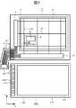
図1は、本発明による液晶表示装置100を示す平面図である。液晶表示装置100は液晶パネル1とバックライト110と制御回路80とで構成される。制御回路80からは液晶パネル1の表示に必要な信号及び、電源電圧が供給される。制御回路80はフレキシブル基板70に搭載されており、配線71、端子75を介して信号が液晶パネル1に伝達される。また、バックライト110にも必要な電圧が配線173を介して供給される。
FIG. 1 is a plan view showing a liquid
バックライト110は、導光板120と光源部130と収納ケース180と光源部130に設けられた発光素子150とから構成されている。バックライト110は液晶パネル1に光を照射する目的で設けられる。液晶パネル1ではバックライト110から照射された光の透過量または反射量を制御して表示を行う。なお、バックライト110は観察者に対して液晶パネル1の裏面側または前面側に重ねて設けられるが、図1では解り易くするために、液晶パネル1と並べて表示している。バックライト110の詳細については後述する。
The
液晶パネル1の画素部8には画素電極12が設けられている。なお、液晶パネル1は多数の画素部8をマトリクス状に備えているが、図が煩雑になることを避けて、図1では画素部8を1つだけ図示している。マトリクス状に配置された画素部8は表示領域9を形成し、各画素部8が表示画像の画素の役割をはたし、表示領域9に画像を表示する。
A
液晶パネル1には、図中x方向に延在しy方向に並設されるゲート信号線(走査線とも呼ぶ)21と、y方向に延在しx方向に並設されるドレイン信号線(映像信号線とも呼ぶ)22とが設けられており、ゲート信号線21とドレイン信号線22とで囲まれる領域に画素部8が形成されている。
The liquid crystal panel 1 includes a gate signal line (also referred to as a scanning line) 21 extending in the x direction and arranged in the y direction and a drain signal line extending in the y direction and arranged in the x direction. The pixel portion 8 is formed in an area surrounded by the
画素部8にはスイッチング素子10が設けられている。ゲート信号線21からは制御信号が供給され、スイッチング素子10のオン・オフが制御される。スイッチング素子10がオン状態となることで、ドレイン信号線22を介して伝送された映像信号が画素電極12に供給される。
A switching element 10 is provided in the pixel portion 8. A control signal is supplied from the
ドレイン信号線22は駆動回路5に接続されており、駆動回路5から映像信号が出力する。ゲート信号線21は駆動回路6に接続されており、駆動回路6からは制御信号が出力する。なお、ゲート信号線21、ドレイン信号線22及び、駆動回路5及び駆動回路6とは同じTFT基板2上に形成されている。また、駆動回路5及び駆動回路6とを一つの半導体素子で形成することも可能である。
The
次に図2に発光素子であるLED150の概略図を示す。図2(a)は概略断面図、図2(b)は光出射側正面図を示す。
Next, FIG. 2 shows a schematic diagram of an
LED150は発光部であるLEDチップ151がチップ基板157に搭載された構造をしている。LEDチップ151はpn接合を有し、pn接合に電圧を印加すると特定の波長の光が出射する。pn接合を形成するp型半導体層にはp電極(アノード)158と、n型半導体層にはn電極(カソード)159とがそれぞれ設けられる。
The
各p電極158と、n電極159にはワイヤ152が接続されている。ワイヤ152はLED150を外部と接続するために設けられたチップ端子153とp電極158及びn電極159とを電気的に接続する。
A
LEDチップ151の出射面側には、蛍光発光部156が設けられる場合もある。蛍光発光部156はLEDチップ151から発光する光の波長を変換する機能を有している。符号157はコーン状反射面で横方向に進む光を出射面側に反射させる。符号166はカソード(またはアノード)の位置を表示するマークである。
A fluorescent
チップ端子153はチップ基板157の裏面で外部配線等と接続するが、チップ基板157の裏面から側面を経て出射面側にまで延伸してチップ搭載部154を形成している。チップ端子153と、チップ搭載部154とを光反射率の高い金属で形成した場合に、チップ搭載部154を光反射面として利用することが可能である。また、チップ端子153と、チップ搭載部154とを熱伝導率の高い金属(導電部材でも良い)で形成すると、LEDチップ151で発生した熱をチップ基板157の裏面側に放熱することが可能である。
The
次に、図3を用いてLEDチップ151が搭載される基板について説明する。図3(a)は金属基板161にLEDチップ151を搭載した様子を示す概略断面図である。図3(b)はLEDチップ151が搭載される部分の概略正面図である。
Next, a substrate on which the
搭載基板160は金属基板161にFPC162を配置し、FPC162上に設けられた銅箔等の導電層で配線163を形成している。配線163の上には絶縁層164がもうけられ、導電層上に形成される絶縁層164の開口部により接続用のパッド165が形成される。
In the mounting
搭載基板160の基材を金属とすることで、チップ基板157の裏面側に伝わった熱を効果的に放熱することが可能である。放熱の効率を上げるためには絶縁層164はショートやリークの問題が生じない程度に薄いことが望ましい。本実施例では絶縁層164の厚さは0.12mmで熱伝導率は6.5W/m・Kの絶縁層を使用した。
By using the base material of the mounting
配線の端部に形成された接続用のパッド165には、LEDチップ151のチップ端子153が電気的に接続される。前述したように搭載基板160の表面には絶縁層164が塗布されており、配線が搭載基板160の表面側で他の構成物とショートすることを防止し、パッド165間の絶縁を保っている。パッド165には半田ペースト等が印刷塗布されリフロー工程等により、LEDチップ151が搭載基板160上に実装される。
The
半田リフロー工程を用いる理由から絶縁層164は半田と親和性が低い部材が選ばれるが、搭載基板160の表面に形成されることから、無彩色のものが好ましい。特に光の利用効率を考慮すると反射光の多い白色か白色に近いものが望ましい。反射率が高い材料としては酸化チタン等が適している。なお、167はカソード(またはアノード)の位置を示すマークである。視認性を高めるため絶縁層164に使用した色とは異なる色が用いられる。
A member having a low affinity for solder is selected for the insulating
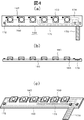
次に図4を用いて、LED150を搭載基板160上に線状に搭載し板状光源130を形成した様子を示す。図4(a)は概略正面図であり、図4(b)は概略断面図で、図4(c)は概略斜視図である。
Next, a state in which the
図4ではLED150は搭載基板160上に6個並べて線状光源となるように配置されている。LED150はダイオードとしての特性からpn接合間で一定の電圧差が生じる。このpn接合間の電圧差は製造プロセスによりばらつく、そのため、最適な電圧がpn接合に印加されるように調整されるが、n個のLED150を並列に接続するとn個の調整回路が必要となり、調整のために製造費用が増加するという問題が生じる。
In FIG. 4, six
図4では3個毎に直列につないで、3個毎に電圧を調整している。電源電圧に車載用途の12Vを使用し、各LED150で生じる電位差が4V程度の場合は3個直列に接続することが効率的である。すなわち、電源電圧Vと、平均的なLED150で生じる電位差Vdと、個数nとの関係を、V>=n×Vdとすると効率が良い。なお、各LED150で生じる電位差が3V程度で、電源電圧が12Vの場合は4個直列に接続すると効率的である。また、n個直列に接続したLED150の最後のLED150と接地電位の間に抵抗172を挿入して調整を行う場合は、直列接続毎に配線が電圧供給用174とリターン用175の2本必要となる。本実施例では配線が4本となり、それぞれの配線は外部接続配線173に接続している。
In FIG. 4, every three pieces are connected in series, and the voltage is adjusted every three pieces. When 12V for in-vehicle use is used as the power supply voltage and the potential difference generated by each
図4(c)に示すように、配線174、175は搭載基板160上に設けられるが、LED150の数が増加すると配線174、175を設ける面積も増加することになる。図中LED150の下側には、LED150の数に従って配線174、175が設けられている。また、回路に必要な抵抗や容量等の電気素子も搭載基板160上に設けられている。
As shown in FIG. 4C, the
次に図5を用いて導光板120と板状光源部130を収納する収納ケース180について説明する。収納ケース180は金属等を箱型に形成し、導光板120を収納可能とした形状をしている。
Next, a
導光板120は入光面125と出光面121と下面122を有し、板状光源部130から入射した光は入光面125から入射し出光面121から出射する。出光面121に対して下面122は傾いており、導光板120は楔型の形状をしている。なお、導光板120は出光面121に対して下面122が一定の厚さ有した楔型でないものを用いることも可能である。
The
収納ケース180は底面185と底面185の四方を囲むように第1の側面181と第2の側面182と第3の側面183と第4の側面184とを備えている。入光面125に対向するよう、第1の側面181は形成されており、第1の側面181には板状光源部130が接着されている。
The
収納ケース180は金属製のため、板状光源部130を収納ケース180に接触させることで、収納ケース180は放熱板の役割を果す。ただし、板状光源部130と入光面125との位置関係は導光板120に入射する光量に影響を及ぼすため、第1の側面182は入光面125に対向し、容易に位置が変動しないよう設けられる。
Since the
収納ケース180と導光板120の間にはクッション材190が設けられていて、振動等による導光板120の移動や破壊を防止している。また、収納ケース180の底面185の上には反射シート115が設けられており、導光板120から漏れ出た光を出光面121側に反射させている。
A
図5に示すように、収納ケース180を箱状に形成してクッション材190を設けることで、収納ケース180に導光板120を収納することは可能であるが、収納ケース180内で導光板120が容易に移動するという問題が生じる。
As shown in FIG. 5, the
そのため、収納ケース180で導光板120を固定しようとすると、LED150と導光板120が接触し、導光板120が傷つくかLED150を破損してしまうことになる。
Therefore, when the
なお、板状光源部130を収納ケース180に接触させることで、収納ケース180に放熱板の役割を持たせたが、板状光源部130のFPC162を直接第1の側面181に貼り付けることも可能である。すなわち、第1の側面181を板状光源部130の一部として用いることで、光源150と収納ケース180とを一体に形成することが可能となる。
The plate-shaped
次に図6に導光板120が傷つく問題を解決するために、樹脂製の固定部材を収納ケース180に設けた構成を示す。収納ケース180の第1の側面181には板状光源部130が貼り付けられ、第2の側面182と第3の側面183には、取付部192が設けられ、固定用樹脂部材191が取り付け可能となっている。
Next, FIG. 6 shows a configuration in which a resin fixing member is provided in the
図6では解り易くするために、固定用樹脂部材191は取付部192から取り外した状態を示している。収納ケース180に固定用樹脂部材191を取り付けて、導光板120を固定保持する。導光板120には固定用凹部126または固定用凹凸部127が形成されており、この固定用凹部126または固定用凹凸部127に固定用樹脂部材191が嵌め合わされる。
In FIG. 6, the fixing
導光板120と固定用樹脂部材191との間で硬さに差がないため、固定用樹脂部材191から導光板120に対し力が加わっても、固定用樹脂部材191により導光板120が容易に傷つくことない。
Since there is no difference in hardness between the
符号186は制御回路基板保持部で、底面185の裏側に液晶表示装置の制御回路基板を保持固定することが可能となっている。
なお、導光板120の入光面125とLED150との距離が変動すると、入射する光量(入光率)が変動するといった問題が生じる。そのため、熱膨張、振動等により入光面125とLED150との距離が容易に変動しないようにする必要がある。そのため、固定用樹脂部材191は導光板120がLED150に向かって移動しないように設けられる。
Note that when the distance between the
すなわち、第1の側面181に板状光源部130を貼り付けたことで、収納ケース180と板状光源部130とを一体に形成することができ、放熱効率を向上させることが可能となるが、収納ケース180と板状光源部130とが一体となったために、収納ケース180と導光板120との位置が変動すると光学的品質を低下させるといった問題が生じることになる。
That is, by attaching the plate-like
図6では、固定用樹脂部材191は、第1の側面182に交差するように形成されている第2の側面182または第3の側面183に取り付けられている。そのため、固定用樹脂部材191により導光板120が第1の側面181側に移動することが規制可能ある。
In FIG. 6, the fixing
次に、図7に固定用樹脂部材191を第2の側面182に取り付けた様子を示す。固定用樹脂部材191には溝193が設けられており、第2の側面182の一部が嵌め込まれている。また、他方の端部にも溝194が設けられ第2の側面182の一部が嵌め込まれている。この溝194は端部途中で止まっており、溝193とは異なる形状をしている。溝193と溝194の形状が異なる理由は、取付方向を間違えないためである。
Next, FIG. 7 shows a state in which the fixing
取付部192に固定された固定用樹脂部材191に対して、導光板120には固定用保持部材191に嵌め込まれるように、固定用凹部126が形成されている。この固定用凹部126が固定用保持部材191に嵌め込まれることで、導光板120は収納ケース180に対して固定される。
With respect to the fixing
取付部192の外側には保持板195が設けられ、固定用樹脂部材191が外側に移動することを規制するとともに、固定用樹脂部材191を保護する役割も有している。
A holding
固定用樹脂部材191の上面には、光学シート保持用溝196が設けられており、導光板120の上に設けられる光学シートを固定用樹脂部材191で保持可能となっている。
An optical
次に図8に固定用樹脂部材191に対して、導光板に固定用凹凸部127を取り付けた様子を示す。図7同様溝193と溝194と保持板195により、収納ケース180の第2の側面182に取り付けられている。
Next, FIG. 8 shows a state in which the fixing
導光板120には固定用保持部材191に嵌め込まれるように、固定用凹凸部127が形成されている。この固定用凹凸部127の凹凸が固定用保持部材191に嵌め込まれることで、導光板120は収納ケース180に対して固定される。
The
図7同様に光学シート保持用溝196が設けられており、導光板120の突起129と同様な幅で、導光板120の上に設けられる光学シートも突出部を有しており、光学シートの突出部を光学シート保持用溝196で保持可能となっている。また、固定用保持部材191は不要な光の反射を防ぐ目的で角部には面取り加工が施される場合がある。
Similar to FIG. 7, an optical
さらに、固定用樹脂部材191の色を黒として反射防止することも可能である。なお、固定用樹脂部材191付近から出射する光量を調整する目的で、固定用樹脂部材191を無彩色としたり、特定の色を付けることも可能である。
Furthermore, it is possible to prevent reflection by setting the color of the fixing
次に、図9を用いて取付部192について説明する。取付部192は第2の側面182または第3の側面183の一部に設けられ、収納ケース180と同じ金属で一体に設けられる。図9(a)は取付部192と固定用樹脂部材191との関係を示しており、矢印方向に固定用樹脂部材191を取付部192に押し込むことで、取付部192に固定用樹脂部材191が取付けられる。
Next, the
前述したように、固定用樹脂部材191には溝193と溝194が設けられており、溝193と194に側面の一部が嵌め込まれることで、固定用樹脂部材191が固定する。なお、溝194は固定用樹脂部材191の下から上まで貫通しておらず、途中で止まっている。そのため、対応する側面の一部には切り欠き197が設けられている。
As described above, the fixing
図9(b)は保持板195の位置を説明するための斜視図である。保持板195は第2の側面182(第3の側面183でも同様である)から外側に突出しており、固定用樹脂部材191を外側から保持可能となっている。
FIG. 9B is a perspective view for explaining the position of the holding
次に図10に導光板120と固定用樹脂部材191と取付部192との関係を斜視図で示す。
Next, FIG. 10 is a perspective view showing the relationship among the
導光板120の固定用凹凸部127が固定用樹脂部材191に嵌め込まれ、固定用樹脂部材191が取付部192に固定されることで、導光板120が収納ケース180に固定されることになる。
The fixing
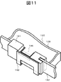
次に、図11に導光板120と固定用樹脂部材191と取付部192とを組合した状態を斜視図で示す。導光板120の上には光学シート128が搭載され、光学シート128の突出部が固定用樹脂部材191の光学シート保持用溝196に配置されている。
Next, FIG. 11 is a perspective view showing a state in which the
導光板120は固定用樹脂部材191により固定され、収納ケース180と接触することがないので、金属製の収納ケースで導光板120が傷つけられることが防止可能である。
Since the
1…液晶パネル、2…TFT基板、5…駆動回路、6…駆動回路、8…画素部、9…表示領域、10…スイッチング素子、12…画素電極、21…ゲート配線(走査信号線)、22…映像信号線、70…FPC、71…配線、75…端子、80…制御回路、110…バックライト、120…導光板、130…板状光源部、150…LED、151…LEDチップ、152…ワイヤ、153…チップ端子、154…チップ搭載部、155…コーン状反射面、156…蛍光発光部、157…チップ基板、158…P電極、159…n電極、160…搭載基板、161…金属基板、162…絶縁層、163…配線、164…表面絶縁層、165…パッド、166…マーク、167…マーク、173…外部接続配線、180…バックライト、181…上側収納ケース、182…下側収納ケース、183…窓、184…係止部、185…係止部、186…収納部、187…導光板収納部、190…クッション材。
DESCRIPTION OF SYMBOLS 1 ... Liquid crystal panel, 2 ... TFT substrate, 5 ... Drive circuit, 6 ... Drive circuit, 8 ... Pixel part, 9 ... Display area, 10 ... Switching element, 12 ... Pixel electrode, 21 ... Gate wiring (scanning signal line), 22 ... Video signal line, 70 ... FPC, 71 ... Wiring, 75 ... Terminal, 80 ... Control circuit, 110 ... Backlight, 120 ... Light guide plate, 130 ... Plate light source unit, 150 ... LED, 151 ... LED chip, 152 ... Wire, 153 ... Chip terminal, 154 ... Chip mounting part, 155 ... Cone reflection surface, 156 ... Fluorescent light emitting part, 157 ... Chip substrate, 158 ... P electrode, 159 ... n electrode, 160 ... Mounting board, 161 ... Metal Substrate, 162 ... insulating layer, 163 ... wiring, 164 ... surface insulating layer, 165 ... pad, 166 ... mark, 167 ... mark, 173 ... external connection wiring, 180 ... backlight, 181 ... Side storage case, 182 ... lower housing case, 183 ... window, 184 ... engaging
Claims (7)
上記バックライトに設けられた複数の発光素子と、
上記発光素子が配置される回路基板と、
上記発光素子の光が入射する導光板と、
上記導光板を収納する収納ケースとを有し、
上記収納ケースは金属により形成され、底面と該底面に交差するように折り曲げられた第1の側面と第2の側面とを有し、
上記第1の側面に上記回路基板を配置し、
上記第1の側面に交差する位置に形成された第2の側面に嵌め込んだ、上記導光板を固定する樹脂部材を取り付けたことを特徴とする液晶表示装置。 A display panel and a backlight for irradiating the display panel with light;
A plurality of light emitting elements provided in the backlight;
A circuit board on which the light emitting element is disposed;
A light guide plate on which light from the light emitting element is incident;
A storage case for storing the light guide plate;
The storage case is made of metal, and has a bottom surface and a first side surface and a second side surface that are bent so as to intersect the bottom surface.
Placing the circuit board on the first side;
A liquid crystal display device, wherein a resin member for fixing the light guide plate, fitted to a second side surface formed at a position intersecting the first side surface, is attached.
該面状光源装置内で線状に配置された発光ダイオードと、
該発光ダイオードを電気的に接続する回路基板と、
上記発光ダイオードの光が入射する入射面を有する導光板と、
上記導光板を収納する金属の収納部とを有し、
上記金属の収納部には上記入射面に対向する第1の側面と上記第1の側面に交差するように第2側面が設けられ、
上記入射面に対向する上記第1の側面には上記回路基板が配置され、
上記金属の収納部の上記第2の側面には上記導光板と上記回路基板との間隔を保つ樹脂部材が嵌め込んで設けられたことを特徴とする液晶表示装置。 A liquid crystal panel, and a planar light source device for irradiating the liquid crystal panel with light,
Light emitting diodes arranged linearly in the planar light source device;
A circuit board for electrically connecting the light emitting diodes;
A light guide plate having an incident surface on which light of the light emitting diode is incident;
A metal housing for housing the light guide plate;
The metal storage portion is provided with a first side surface facing the incident surface and a second side surface so as to intersect the first side surface,
The circuit board is disposed on the first side surface facing the incident surface,
A liquid crystal display device, wherein a resin member that keeps a distance between the light guide plate and the circuit board is fitted into the second side surface of the metal storage portion.
6. The liquid crystal display device according to claim 5, wherein the circuit board is provided with a flexible board on a metal plate.
Priority Applications (3)
| Application Number | Priority Date | Filing Date | Title |
|---|---|---|---|
| JP2007240398A JP5074135B2 (en) | 2007-09-18 | 2007-09-18 | Liquid crystal display |
| US12/230,912 US7855761B2 (en) | 2007-09-18 | 2008-09-08 | Liquid crystal display device |
| CNA2008101489147A CN101393357A (en) | 2007-09-18 | 2008-09-17 | Liquid crystal display device |
Applications Claiming Priority (1)
| Application Number | Priority Date | Filing Date | Title |
|---|---|---|---|
| JP2007240398A JP5074135B2 (en) | 2007-09-18 | 2007-09-18 | Liquid crystal display |
Publications (3)
| Publication Number | Publication Date |
|---|---|
| JP2009069713A JP2009069713A (en) | 2009-04-02 |
| JP2009069713A5 JP2009069713A5 (en) | 2010-11-04 |
| JP5074135B2 true JP5074135B2 (en) | 2012-11-14 |
Family
ID=40493708
Family Applications (1)
| Application Number | Title | Priority Date | Filing Date |
|---|---|---|---|
| JP2007240398A Active JP5074135B2 (en) | 2007-09-18 | 2007-09-18 | Liquid crystal display |
Country Status (3)
| Country | Link |
|---|---|
| US (1) | US7855761B2 (en) |
| JP (1) | JP5074135B2 (en) |
| CN (1) | CN101393357A (en) |
Families Citing this family (18)
| Publication number | Priority date | Publication date | Assignee | Title |
|---|---|---|---|---|
| JP5074135B2 (en) * | 2007-09-18 | 2012-11-14 | 株式会社ジャパンディスプレイイースト | Liquid crystal display |
| KR20100057710A (en) * | 2008-11-10 | 2010-06-01 | 삼성전자주식회사 | Light emitting diodes and backlight unit having the same |
| JP5320250B2 (en) * | 2009-10-14 | 2013-10-23 | 株式会社日立製作所 | Transparent structure, light source module, and illumination device, liquid crystal display device, and video display device using the same |
| JP5729581B2 (en) * | 2009-11-12 | 2015-06-03 | Nltテクノロジー株式会社 | Surface emitting device |
| KR101698816B1 (en) * | 2009-11-30 | 2017-01-24 | 삼성디스플레이 주식회사 | Backlight assembly |
| JP2012150868A (en) * | 2011-01-20 | 2012-08-09 | Sanyo Electric Co Ltd | Printed wiring board |
| JP2012231083A (en) * | 2011-04-27 | 2012-11-22 | Hitachi Consumer Electronics Co Ltd | Back light and liquid crystal display unit using the same |
| US20140347596A1 (en) * | 2011-12-06 | 2014-11-27 | SHARP KABUSHIKI KAISHA a corporation | Backlight unit and liquid-crystal display device |
| US8398288B1 (en) * | 2012-04-03 | 2013-03-19 | Giantech Industries Co., Ltd. | LED display frame structure |
| KR20140020014A (en) | 2012-08-07 | 2014-02-18 | 삼성디스플레이 주식회사 | Backlight device, display device including the same and manufacturing method for backlight device |
| KR102013834B1 (en) | 2012-08-10 | 2019-08-26 | 삼성디스플레이 주식회사 | Backlight and display device including the same |
| CN102889519A (en) * | 2012-09-18 | 2013-01-23 | 深圳市华星光电技术有限公司 | Backlight module and display panel |
| TWM450828U (en) * | 2012-12-14 | 2013-04-11 | Litup Technology Co Ltd | LED module with separate heat-dissipation and electrical conduction paths, and related heat dissipation board |
| CN103454796A (en) * | 2013-08-15 | 2013-12-18 | Tcl王牌电器(惠州)有限公司 | Self-adaptive assembly method and system for flat panel display device |
| CN107783222B (en) * | 2016-08-26 | 2020-07-14 | 美蓓亚三美株式会社 | Planar lighting device and substrate |
| JP6462032B2 (en) * | 2016-08-26 | 2019-01-30 | ミネベアミツミ株式会社 | Surface illumination device and substrate |
| CN108159574A (en) * | 2018-02-13 | 2018-06-15 | 武汉中科科理光电技术有限公司 | Heat radiation protection device and spectral therapeutic instrumnt |
| US20190364669A1 (en) * | 2018-05-25 | 2019-11-28 | Nichia Corporation | Method for manufacturing light emitting module |
Family Cites Families (10)
| Publication number | Priority date | Publication date | Assignee | Title |
|---|---|---|---|---|
| JP3891843B2 (en) * | 2002-01-08 | 2007-03-14 | 株式会社日立製作所 | Liquid crystal display |
| JP2003281924A (en) | 2002-03-22 | 2003-10-03 | Sony Corp | Light source device, manufacturing method for the same, planar lighting device, and liquid crystal display device |
| JP2004021238A (en) * | 2002-06-20 | 2004-01-22 | Nec Saitama Ltd | Display device and mobile terminal system |
| KR100989338B1 (en) * | 2003-07-01 | 2010-10-25 | 삼성전자주식회사 | Backlight assembly and liquid crystal display device having the same |
| JP5072186B2 (en) | 2005-02-25 | 2012-11-14 | 京セラ株式会社 | Liquid crystal display |
| JP4683274B2 (en) * | 2005-04-26 | 2011-05-18 | ミネベア株式会社 | Surface lighting device |
| JP2007163556A (en) * | 2005-12-09 | 2007-06-28 | Hitachi Displays Ltd | Liquid crystal display device |
| JP2007163620A (en) * | 2005-12-12 | 2007-06-28 | Hitachi Displays Ltd | Liquid crystal display device and backlight device |
| KR100852250B1 (en) * | 2006-01-18 | 2008-08-14 | 미쓰비시덴키 가부시키가이샤 | Planar light source unit and image display apparatus using the same |
| JP5074135B2 (en) * | 2007-09-18 | 2012-11-14 | 株式会社ジャパンディスプレイイースト | Liquid crystal display |
-
2007
- 2007-09-18 JP JP2007240398A patent/JP5074135B2/en active Active
-
2008
- 2008-09-08 US US12/230,912 patent/US7855761B2/en active Active
- 2008-09-17 CN CNA2008101489147A patent/CN101393357A/en active Pending
Also Published As
| Publication number | Publication date |
|---|---|
| US7855761B2 (en) | 2010-12-21 |
| US20090185099A1 (en) | 2009-07-23 |
| CN101393357A (en) | 2009-03-25 |
| JP2009069713A (en) | 2009-04-02 |
Similar Documents
| Publication | Publication Date | Title |
|---|---|---|
| JP5074135B2 (en) | Liquid crystal display | |
| JP4959506B2 (en) | Liquid crystal display | |
| JP5295523B2 (en) | Liquid crystal display | |
| US20090316063A1 (en) | Liquid crystal display device | |
| KR101546741B1 (en) | Light emitting module and display apparatus having the same | |
| JP5097461B2 (en) | Liquid crystal display and backlight module thereof | |
| JP2007279480A (en) | Liquid crystal display device | |
| US7717605B2 (en) | Liquid crystal display device | |
| US7478925B2 (en) | Lighting source unit, illuminating apparatus using the same and display apparatus using the same | |
| US8439513B2 (en) | Light emitting diode module and back light assembly | |
| US20100277670A1 (en) | Backlight unit and liquid crystal display device | |
| US20060220030A1 (en) | Lighting device with flipped side-structure of LEDs | |
| KR101164976B1 (en) | Heat radiating printed circuit boad unified bracket and chassis structure having the same | |
| KR20150033169A (en) | Light emitting diode package and liquid crystal display device using the same | |
| WO2011162016A1 (en) | Led backlight device and liquid crystal display device | |
| JP2006310221A (en) | Edge input type backlight and liquid crystal display device | |
| JP2011134474A (en) | Surface light emitting device | |
| JP2007286467A (en) | Back-light device and liquid crystal display device | |
| JP4160444B2 (en) | Planar light source device and display device using the same | |
| KR20100134494A (en) | Light emitting diode package, and back-light unit and liquid crystal display device using the same | |
| JP2008027916A (en) | Backlight assembly, its manufacturing method, and display device including it | |
| JP2007109945A (en) | Light source | |
| JP4113832B2 (en) | Planar light source device and liquid crystal display device using the same | |
| KR200154173Y1 (en) | Frame structure both for cooling plate and led module | |
| KR101266703B1 (en) | Liquid crystal display divice |
Legal Events
| Date | Code | Title | Description |
|---|---|---|---|
| RD02 | Notification of acceptance of power of attorney |
Free format text: JAPANESE INTERMEDIATE CODE: A7422 Effective date: 20100127 |
|
| RD04 | Notification of resignation of power of attorney |
Free format text: JAPANESE INTERMEDIATE CODE: A7424 Effective date: 20100225 |
|
| A521 | Request for written amendment filed |
Free format text: JAPANESE INTERMEDIATE CODE: A523 Effective date: 20100916 |
|
| A621 | Written request for application examination |
Free format text: JAPANESE INTERMEDIATE CODE: A621 Effective date: 20100916 |
|
| A711 | Notification of change in applicant |
Free format text: JAPANESE INTERMEDIATE CODE: A711 Effective date: 20110328 |
|
| A977 | Report on retrieval |
Free format text: JAPANESE INTERMEDIATE CODE: A971007 Effective date: 20120516 |
|
| A131 | Notification of reasons for refusal |
Free format text: JAPANESE INTERMEDIATE CODE: A131 Effective date: 20120619 |
|
| A521 | Request for written amendment filed |
Free format text: JAPANESE INTERMEDIATE CODE: A523 Effective date: 20120711 |
|
| TRDD | Decision of grant or rejection written | ||
| A01 | Written decision to grant a patent or to grant a registration (utility model) |
Free format text: JAPANESE INTERMEDIATE CODE: A01 Effective date: 20120731 |
|
| A01 | Written decision to grant a patent or to grant a registration (utility model) |
Free format text: JAPANESE INTERMEDIATE CODE: A01 |
|
| A61 | First payment of annual fees (during grant procedure) |
Free format text: JAPANESE INTERMEDIATE CODE: A61 Effective date: 20120823 |
|
| R150 | Certificate of patent or registration of utility model |
Ref document number: 5074135 Country of ref document: JP Free format text: JAPANESE INTERMEDIATE CODE: R150 Free format text: JAPANESE INTERMEDIATE CODE: R150 |
|
| FPAY | Renewal fee payment (event date is renewal date of database) |
Free format text: PAYMENT UNTIL: 20150831 Year of fee payment: 3 |
|
| R250 | Receipt of annual fees |
Free format text: JAPANESE INTERMEDIATE CODE: R250 |
|
| R250 | Receipt of annual fees |
Free format text: JAPANESE INTERMEDIATE CODE: R250 |
|
| R250 | Receipt of annual fees |
Free format text: JAPANESE INTERMEDIATE CODE: R250 |
|
| R250 | Receipt of annual fees |
Free format text: JAPANESE INTERMEDIATE CODE: R250 |
|
| R250 | Receipt of annual fees |
Free format text: JAPANESE INTERMEDIATE CODE: R250 |
|
| R250 | Receipt of annual fees |
Free format text: JAPANESE INTERMEDIATE CODE: R250 |
|
| S531 | Written request for registration of change of domicile |
Free format text: JAPANESE INTERMEDIATE CODE: R313531 |
|
| S533 | Written request for registration of change of name |
Free format text: JAPANESE INTERMEDIATE CODE: R313533 |
|
| R350 | Written notification of registration of transfer |
Free format text: JAPANESE INTERMEDIATE CODE: R350 |
|
| R250 | Receipt of annual fees |
Free format text: JAPANESE INTERMEDIATE CODE: R250 |
|
| R250 | Receipt of annual fees |
Free format text: JAPANESE INTERMEDIATE CODE: R250 |
|
| R250 | Receipt of annual fees |
Free format text: JAPANESE INTERMEDIATE CODE: R250 |
|
| S111 | Request for change of ownership or part of ownership |
Free format text: JAPANESE INTERMEDIATE CODE: R313117 |
|
| R350 | Written notification of registration of transfer |
Free format text: JAPANESE INTERMEDIATE CODE: R350 |