JP5046565B2 - Method for manufacturing semiconductor device - Google Patents
Method for manufacturing semiconductor device Download PDFInfo
- Publication number
- JP5046565B2 JP5046565B2 JP2006160027A JP2006160027A JP5046565B2 JP 5046565 B2 JP5046565 B2 JP 5046565B2 JP 2006160027 A JP2006160027 A JP 2006160027A JP 2006160027 A JP2006160027 A JP 2006160027A JP 5046565 B2 JP5046565 B2 JP 5046565B2
- Authority
- JP
- Japan
- Prior art keywords
- region
- film
- semiconductor layer
- layer
- gate electrode
- Prior art date
- Legal status (The legal status is an assumption and is not a legal conclusion. Google has not performed a legal analysis and makes no representation as to the accuracy of the status listed.)
- Expired - Fee Related
Links
Images


Description
本発明は薄膜トランジスタ(以下、TFTという)で構成された回路を有する半導体装置およびその作製方法に関する。例えば、液晶表示パネルに代表される電気光学装置や有機発光素子を有する発光表示装置を部品として搭載した電子機器に関する。 The present invention relates to a semiconductor device having a circuit formed of a thin film transistor (hereinafter referred to as TFT) and a manufacturing method thereof. For example, the present invention relates to an electronic apparatus in which an electro-optical device typified by a liquid crystal display panel or a light-emitting display device having an organic light-emitting element is mounted as a component.
なお、本明細書中において半導体装置とは、半導体特性を利用することで機能しうる装置全般を指し、電気光学装置、半導体回路および電子機器は全て半導体装置である。 Note that in this specification, a semiconductor device refers to all devices that can function by utilizing semiconductor characteristics, and an electro-optical device, a semiconductor circuit, and an electronic device are all semiconductor devices.
近年、絶縁表面を有する基板上に形成された半導体薄膜(厚さ数〜数百nm程度)を用いて薄膜トランジスタ(TFT)を構成する技術が注目されている。薄膜トランジスタはICや電気光学装置のような電子デバイスに広く応用され、特に画像表示装置のスイッチング素子として開発が急がれている。 In recent years, a technique for forming a thin film transistor (TFT) using a semiconductor thin film (having a thickness of about several to several hundred nm) formed on a substrate having an insulating surface has attracted attention. Thin film transistors are widely applied to electronic devices such as ICs and electro-optical devices, and development of switching devices for image display devices is urgently required.
特に、マトリクス状に配置された表示画素毎にTFTからなるスイッチング素子を設けたアクティブマトリクス型の表示装置(液晶表示装置や発光表示装置)が盛んに開発されている。 In particular, active matrix display devices (liquid crystal display devices and light-emitting display devices) in which switching elements made of TFTs are provided for each display pixel arranged in a matrix have been actively developed.
アクティブマトリクス型の表示装置においては、画素部において有効画面領域を広げる開発が進められている。有効画面領域の面積を大きくするには画素部に配置されるTFT(画素TFT)の占める面積をできるだけ小さくする必要に迫られている。また、製造コストの低減を図るために駆動回路を画素部と同一基板上に作り込む開発も進められている。中でも、ポリシリコン膜を用いたTFTは、アモルファスシリコン膜を用いたTFTよりも電界効果移動度が高いので高速動作が可能である。 In an active matrix display device, development for expanding an effective screen area in a pixel portion is underway. In order to increase the area of the effective screen area, it is necessary to reduce the area occupied by TFTs (pixel TFTs) arranged in the pixel portion as much as possible. In addition, in order to reduce the manufacturing cost, development in which a driver circuit is formed on the same substrate as the pixel portion is also in progress. In particular, a TFT using a polysilicon film has a higher field effect mobility than a TFT using an amorphous silicon film, and can operate at high speed.
表示装置に搭載されるモジュールには、機能ブロックごとに画像表示を行う画素部や、CMOS回路を基本としたシフトレジスタ回路、レベルシフタ回路、バッファ回路、サンプリング回路などの画素部を制御するための駆動回路が一枚の基板上に形成される。 The module mounted on the display device includes a pixel unit for displaying an image for each functional block, and a drive for controlling the pixel unit such as a shift register circuit, a level shifter circuit, a buffer circuit, and a sampling circuit based on a CMOS circuit. A circuit is formed on a single substrate.
同一基板上に駆動回路と画素部を形成した場合、駆動回路をTAB方式で実装したものと比べて、額縁部と呼ばれる画素領域以外の領域が占める面積が大きくなる傾向がある。額縁部の面積を小さくするために、駆動回路を構成する回路規模を小さくする必要にも迫られている。 When the driver circuit and the pixel portion are formed over the same substrate, an area occupied by a region other than the pixel region called a frame portion tends to be larger than that in which the driver circuit is mounted by the TAB method. In order to reduce the area of the frame portion, there is an urgent need to reduce the circuit scale constituting the drive circuit.
特に、有機発光素子(EL素子)をマトリクス状に配置した発光表示装置においては、1つの画素に役割の異なる複数のTFTが必要とされている。また、液晶表示装置においても、1つの画素にスイッチング用のTFTとSRAMなどの記憶素子とを形成する試みがなされている。また、同一基板上に画素部と駆動回路とを形成する場合においても、できるだけ小型化することが望まれている。 In particular, in a light emitting display device in which organic light emitting elements (EL elements) are arranged in a matrix, a plurality of TFTs having different roles are required for one pixel. In liquid crystal display devices, an attempt is made to form a switching TFT and a storage element such as an SRAM in one pixel. Further, even when the pixel portion and the driver circuit are formed on the same substrate, it is desired to reduce the size as much as possible.
特許文献1は、片側側部が薄いゲート電極を有する電界効果トランジスタが開示されている。特許文献1の電界効果トランジスタは、ゲート電極の形状を断面L字状とし、そのL字の背面部に沿って側壁スペーサを形成し、その側壁スペーサを設けたゲート電極をマスクとして高濃度にイオンを注入することでドレイン側にのみ低濃度ドレインを有する(LDD:Lightly Doped Drain)構造としている。また、ゲート電極のL字の表面にシリサイド層を形成している。 Patent Document 1 discloses a field effect transistor having a gate electrode that is thin on one side. In the field effect transistor of Patent Document 1, the gate electrode has an L-shaped cross section, a side wall spacer is formed along the L-shaped back surface, and the gate electrode provided with the side wall spacer is used as a mask to form a high concentration ion. In this case, a lightly doped drain (LDD) structure is formed only on the drain side. A silicide layer is formed on the L-shaped surface of the gate electrode.
また、特許文献2は、片側にLDD領域を有する薄膜トランジスタが開示されている。特許文献2の薄膜トランジスタは、ゲート電極の一側のみに側壁スペーサを設けている。特許文献2には、イオン注入の時、側壁スペーサをマスクとして側壁スペーサの下部の高濃度ドレイン領域は、傾斜した接続構造を有し、この傾斜した接合構造はLDD構造と同一の効果があると記載されている。 Patent Document 2 discloses a thin film transistor having an LDD region on one side. In the thin film transistor of Patent Document 2, a sidewall spacer is provided only on one side of the gate electrode. In Patent Document 2, when ion implantation is performed, the high concentration drain region under the side wall spacer has an inclined connection structure using the side wall spacer as a mask, and the inclined junction structure has the same effect as the LDD structure. Are listed.
また、特許文献3は、ソース側とドレイン側で幅の異なるサイドウォールを形成し、高濃度不純物拡散層形成のためのイオン注入を行う半導体装置の作製方法が開示されている。 Patent Document 3 discloses a method for manufacturing a semiconductor device in which sidewalls having different widths are formed on the source side and the drain side, and ion implantation for forming a high concentration impurity diffusion layer is performed.
また、本出願人は、回折格子パターン或いは半透膜からなる光強度低減機能を有する補助パターンを設置したフォトマスク或いはレチクルをゲート電極形成用フォトリソグラフィ工程に適用したTFT作製工程を特許文献4で開示している。 In addition, the present applicant has disclosed a TFT manufacturing process in which a photomask or a reticle provided with an auxiliary pattern having a function of reducing light intensity made of a diffraction grating pattern or a semi-transmissive film is applied to a gate electrode forming photolithography process in Patent Document 4. Disclosure.
また、本出願人は、ゲート電極が2層、且つ、片側にLDD領域を有する薄膜トランジスタを特許文献5で開示している。
上述した特許文献1、特許文献2、及び特許文献3の技術は、いずれも側壁スペーサ(サイドウォールとも呼ばれる)を形成する工程を必要不可欠としている。 The techniques of Patent Document 1, Patent Document 2, and Patent Document 3 described above all require a step of forming sidewall spacers (also referred to as sidewalls).
本発明は、側壁スペーサを形成することなく、且つ、工程数を増やすことなく、自己整合的にLDD領域を少なくとも一つ備えたTFTを提供する。 The present invention provides a TFT including at least one LDD region in a self-aligning manner without forming a sidewall spacer and without increasing the number of steps.
また、同一基板上に、工程数を増やすことなく、様々なTFT、例えば、チャネル形成領域の片側にLDD領域を有するTFTと、チャネル形成領域の両側にLDD領域を有するTFTとを形成する作製方法を提供する。 Further, a manufacturing method of forming various TFTs, for example, a TFT having an LDD region on one side of a channel formation region and a TFT having LDD regions on both sides of the channel formation region on the same substrate without increasing the number of steps. I will provide a.
また、側壁スペーサの幅(チャネル長方向の長さ)は、エッチバックする前の絶縁膜の膜厚に依存し、例えば0.5μm以上とすることは困難である。従って、特許文献1、特許文献2、及び特許文献3の技術は、自己整合的に0.5μm以上の幅を有するLDD領域の形成も困難である。本発明は、自己整合的に0.5μm以上の幅を有するLDD領域の形成を実現することも課題としている。 Further, the width of the sidewall spacer (the length in the channel length direction) depends on the film thickness of the insulating film before the etch-back, and it is difficult to set it to, for example, 0.5 μm or more. Therefore, it is difficult for the techniques of Patent Document 1, Patent Document 2, and Patent Document 3 to form an LDD region having a width of 0.5 μm or more in a self-aligned manner. Another object of the present invention is to realize formation of an LDD region having a width of 0.5 μm or more in a self-aligning manner.
また、本発明は、液晶表示装置に代表される電気光学装置、EL素子を有する発光装置、ならびに半導体装置において、今後のさらなる高精細化(画素数の増大)、小型化に伴う各表示画素ピッチの微細化、及び画素部を駆動する駆動回路の集積化を進められるように、複数の素子を限られた面積に形成し、素子が占める面積を縮小して集積することを課題とする。そして、電気光学装置や発光装置の画質を向上させる、或いは様々な回路を集積化して小型化を図ることにより、それを備える電子機器の品質を向上させることを課題とする。 In addition, the present invention relates to an electro-optical device typified by a liquid crystal display device, a light emitting device having an EL element, and a semiconductor device. It is an object to form a plurality of elements in a limited area and reduce the area occupied by the elements so that the elements can be miniaturized and the driving circuit for driving the pixel portion can be integrated. It is another object of the present invention to improve the quality of an electronic apparatus including the electro-optical device and the light-emitting device by improving the image quality or by integrating various circuits to reduce the size.
また、本発明は、動作性能および信頼性の高い回路を備えた半導体装置を提供することを課題とする。そして、半導体装置の信頼性を向上させることにより、それを備える電子機器の信頼性を向上させることを課題とする。 It is another object of the present invention to provide a semiconductor device including a circuit with high operation performance and high reliability. It is an object to improve the reliability of an electronic device including the semiconductor device by improving the reliability of the semiconductor device.
本発明は、回折格子パターン或いは半透膜からなる光強度低減機能を有する補助パターンを設置したフォトマスクまたはレチクルをゲート電極形成用のフォトリソグラフィ工程に適用して膜厚の厚い領域と、片側側部に前記領域より膜厚の薄い領域を有する左右非対称のレジストパターン(レジストパターンの断面形状がゲート電極の幅、または長手方向に非対称形)を形成し、段差を有するゲート電極を形成し、ゲート電極の膜厚の薄い領域を通過させて半導体層に不純物元素を注入して、自己整合的にLDD領域を形成する作製方法を特徴の一つとしている。本発明のTFT構造は、チャネル形成領域と、高濃度に不純物元素を添加して形成するドレイン領域との間に低濃度に不純物元素を添加した領域を一つ設けたものであり、この領域をLDD領域と呼ぶ。 In the present invention, a photomask or a reticle provided with an auxiliary pattern having a light intensity reduction function consisting of a diffraction grating pattern or a semi-transmissive film is applied to a photolithography process for forming a gate electrode, Forming a laterally asymmetric resist pattern (a cross-sectional shape of the resist pattern is asymmetrical in the width of the gate electrode or in the longitudinal direction) having a region thinner than the region in the portion, forming a gate electrode having a step, and forming a gate One feature is a manufacturing method in which an LDD region is formed in a self-aligned manner by injecting an impurity element into a semiconductor layer through a thin region of an electrode. In the TFT structure of the present invention, one region doped with an impurity element at a low concentration is provided between a channel formation region and a drain region formed by adding an impurity element at a high concentration. This is called an LDD region.
また、得られる構造も本発明の特徴の一つであり、段差を有するゲート電極、即ち、膜厚の厚い領域と、片側側部に前記領域より膜厚の薄い領域を有するゲート電極を有し、ゲート電極の膜厚の薄い領域と絶縁層を介して重なるLDD領域を有していることを特徴の一つとしている。ゲート電極の膜厚の薄い領域と絶縁層を介して重なるLDD領域を有している構造とすることで、ドレイン近傍の電界強度が緩和されてホットキャリア注入を防ぎ、劣化現象の防止に有効である。 The obtained structure is also one of the characteristics of the present invention, and includes a gate electrode having a step, that is, a gate electrode having a thick film region and a thin film region on one side portion than the above region. One feature is that it has an LDD region which overlaps with a thin region of the gate electrode with an insulating layer interposed therebetween. The structure having an LDD region that overlaps with the thin region of the gate electrode through an insulating layer reduces the electric field strength near the drain, prevents hot carrier injection, and is effective in preventing deterioration. is there.
また、ゲート電極と重なるLDD領域をLov領域とも呼ぶ。特許文献4では、左右対称のレジストパターンを形成し、チャネル形成領域の両側にLov領域を形成する構成を開示している。一方、本発明は、左右非対称のレジストパターンを形成し、チャネル形成領域の片側にLov領域を形成する構成を開示する。 The LDD region overlapping with the gate electrode is also referred to as a Lov region. Patent Document 4 discloses a configuration in which a symmetrical resist pattern is formed and Lov regions are formed on both sides of a channel formation region. On the other hand, the present invention discloses a configuration in which a left-right asymmetric resist pattern is formed and a Lov region is formed on one side of the channel formation region.
本明細書で開示する発明の構成は、絶縁表面を有する基板上方に半導体層と、前記半導体層上方にゲート絶縁層と、前記ゲート絶縁層上に導電層の積層からなるゲート電極とを有し、前記半導体層は、チャネル形成領域と、前記チャネル形成領域の両側に2つの第1の不純物領域と、一方の第1の不純物領域と前記チャネル形成領域との間に一つの第2の不純物領域とを含み、ゲート電極の積層の一つを構成する第1の導電層は、チャネル形成領域及び第2の不純物領域と少なくとも重なり、ゲート電極の積層の一つを構成する第2の導電層は、第1の導電層上に接し、且つ、前記チャネル形成領域と重なる半導体装置である。 The structure of the invention disclosed in this specification includes a semiconductor layer above a substrate having an insulating surface, a gate insulating layer above the semiconductor layer, and a gate electrode including a conductive layer stacked over the gate insulating layer. The semiconductor layer includes a channel formation region, two first impurity regions on both sides of the channel formation region, and one second impurity region between one first impurity region and the channel formation region. A first conductive layer constituting one of the gate electrode stacks at least overlaps with the channel formation region and the second impurity region, and a second conductive layer constituting one of the gate electrode stacks is The semiconductor device is in contact with the first conductive layer and overlaps the channel formation region.
上記構成において、前記第1の導電層と前記第2の導電層は、異なる材料であることを特徴の一つとしている。前記第1の導電層と前記第2の導電層とを異なる材料とすることで、エッチングレートに差を設けることができ、より上記構成を形成しやすくすることができる。 In the above structure, the first conductive layer and the second conductive layer are made of different materials. By using different materials for the first conductive layer and the second conductive layer, a difference in etching rate can be provided, and the above structure can be more easily formed.
また、上記構成において、前記第1の導電層の膜厚は、前記第2の導電層よりも薄いことを特徴の一つとしている。前記第1の導電層を薄くすることによって、不純物元素を第1の導電層を通過させて半導体層に添加する際、第2の不純物領域の形成を形成しやすくすることができる。 One feature of the above structure is that the first conductive layer is thinner than the second conductive layer. By thinning the first conductive layer, the formation of the second impurity region can be facilitated when the impurity element is added to the semiconductor layer through the first conductive layer.
また、前記第2の導電層の幅は、前記チャネル形成領域の幅と同一であることを特徴の一つとしている。第2の導電層の幅が、チャネル形成領域の幅と同一であることは、第1の不純物領域及び第2の不純物領域が自己整合的に形成されていることを示している。 One feature is that the width of the second conductive layer is the same as the width of the channel formation region. That the width of the second conductive layer is the same as the width of the channel formation region indicates that the first impurity region and the second impurity region are formed in a self-aligned manner.
また、同一基板上に異なる構造のTFTを同時に作製することができ、他の発明の構成は、同一基板上に第1の半導体層を有する第1の薄膜トランジスタと、第2の半導体層を有する第2の薄膜トランジスタとを有する半導体装置であり、絶縁表面を有する基板上方に第1の半導体層及び該第1の半導体層と離間して配置された第2の半導体層と、前記第1の半導体層及び第2の半導体層上方にゲート絶縁層と、前記ゲート絶縁層上に導電層の積層からなる第1のゲート電極及び第2のゲート電極とを有し、前記第1の半導体層は、第1のチャネル形成領域と、前記第1のチャネル形成領域の両側に2つの第1の不純物領域と、一方の第1の不純物領域と前記第1のチャネル形成領域との間に一つの第2の不純物領域とを含み、前記第1のチャネル形成領域は、ゲート絶縁層を介して第1のゲート電極と重なり、第1のゲート電極の積層の一つを構成する第1の導電層は、第1のチャネル形成領域及び第2の不純物領域と少なくとも重なり、第1のゲート電極の積層の一つを構成する第2の導電層は、第1の導電層上に接し、且つ、前記第1のチャネル形成領域と重なり、前記第2の半導体層は、第2のチャネル形成領域と、前記第2のチャネル形成領域の両側に2つの第1の不純物領域と、該第1の不純物領域と前記第2のチャネル形成領域との間に一つの第2の不純物領域とを含み、前記第2のチャネル形成領域は、ゲート絶縁層を介して第2のゲート電極と重なっており、第2のゲート電極の積層の一つを構成する第1の導電層は、第2のチャネル形成領域及び2つの第2の不純物領域と少なくとも重なり、第2のゲート電極の積層の一つを構成する第2の導電層は、第1の導電層上に接し、且つ、前記第2のチャネル形成領域と重なっている半導体装置である。 Further, TFTs having different structures can be formed over the same substrate at the same time, and the structure of another invention is that a first thin film transistor having a first semiconductor layer and a second semiconductor layer having a second semiconductor layer on the same substrate. A first semiconductor layer, a second semiconductor layer disposed apart from the first semiconductor layer above the substrate having an insulating surface, and the first semiconductor layer And a gate insulating layer above the second semiconductor layer, and a first gate electrode and a second gate electrode formed by stacking conductive layers on the gate insulating layer, and the first semiconductor layer includes: One channel formation region, two first impurity regions on both sides of the first channel formation region, and one second impurity region between one first impurity region and the first channel formation region. An impurity region, and the first chip The channel formation region overlaps with the first gate electrode with the gate insulating layer interposed therebetween, and the first conductive layer constituting one of the stacks of the first gate electrode includes the first channel formation region and the second impurity. A second conductive layer at least overlapping with the region and constituting one of the first gate electrode stacks is in contact with the first conductive layer and overlaps with the first channel formation region; The semiconductor layer includes a second channel formation region, two first impurity regions on both sides of the second channel formation region, and a gap between the first impurity region and the second channel formation region. And the second channel formation region overlaps the second gate electrode with a gate insulating layer interposed therebetween, and constitutes one of the stacks of the second gate electrodes. The conductive layer includes a second channel formation region and two second The second conductive layer that overlaps at least the pure region and constitutes one of the stacks of the second gate electrodes is in contact with the first conductive layer and overlaps the second channel formation region Device.
上記構成によって、チャネル形成領域の両側にLDD領域を2つ有するTFTと、チャネル形成領域の片側に1つ有するTFTとを同一基板上に形成し、それぞれに適した回路に用いることができる。片側にLDD領域を有するトランジスタは、ソース及びドレイン電極間に正電圧のみ、もしくは負電圧のみが印加されるトランジスタに適用すればよい。具体的には、インバータ回路、NAND回路、NOR回路、ラッチ回路といった論理ゲートを構成するトランジスタや、センスアンプ、定電圧発生回路、VCOといったアナログ回路を構成するトランジスタに適用すればよい。 With the above structure, a TFT having two LDD regions on both sides of a channel formation region and a TFT having one LDD region on both sides of the channel formation region can be formed over the same substrate and used for a circuit suitable for each. A transistor having an LDD region on one side may be applied to a transistor to which only a positive voltage or only a negative voltage is applied between the source and drain electrodes. Specifically, it may be applied to a transistor constituting a logic gate such as an inverter circuit, a NAND circuit, a NOR circuit, or a latch circuit, or a transistor constituting an analog circuit such as a sense amplifier, a constant voltage generation circuit, or a VCO.
また、上記構造を実現するための作製工程も発明の一つであり、その発明の構成は、半導体層上に絶縁膜を形成し、前記絶縁膜上に導電膜を形成し、前記導電膜上に、回折格子パターン、或いは半透部を有するフォトマスク又はレチクルを用いて、膜厚の厚い領域と、片側側部に前記領域より膜厚の薄い領域とを有するレジストパターンを形成し、前記導電膜のエッチングを選択的に行って、膜厚の厚い領域と、片側側部に前記領域より膜厚の薄い領域とを有するゲート電極を形成し、前記ゲート電極の膜厚の厚い領域及び膜厚の薄い領域をマスクとして前記半導体層に不純物元素を注入して、前記半導体層のうちゲート電極に重なるチャネル形成領域の両側に位置する第1の不純物領域と、前記ゲート電極の膜厚の薄い領域を通過させて前記半導体層に不純物元素を注入して、前記半導体層のうち膜厚の薄い前記ゲート電極と重なる領域に第2の不純物領域とを形成する。なお、回折格子パターン、或いは半透部を有するフォトマスク又はレチクルを用いることによって、前記レジストパターンの断面形状はゲート電極の幅または長さ方向に実質的に非対称となるように形成することを特徴としている。本明細書では、断面形状とは、基板平面に垂直な面で切断した面を指すものとする。 Further, a manufacturing process for realizing the above structure is also one of the inventions, and the structure of the invention is that an insulating film is formed over a semiconductor layer, a conductive film is formed over the insulating film, and the conductive film is formed over the conductive film. Then, a resist pattern having a thick film region and a thin film region on one side is formed using a diffraction grating pattern or a photomask or reticle having a semi-transmissive portion, and the conductive The film is selectively etched to form a gate electrode having a thick region and a region having a thickness smaller than the region on one side, and the gate electrode has a thick region and a film thickness. A first impurity region located on both sides of a channel formation region overlapping the gate electrode in the semiconductor layer, and a thin region of the gate electrode Before letting By injecting an impurity element into the semiconductor layer, and second impurity regions in a region which overlaps with the thin the gate electrode film thickness of the semiconductor layer. Note that by using a diffraction mask pattern or a photomask or reticle having a semi-transmissive portion, the cross-sectional shape of the resist pattern is formed so as to be substantially asymmetric in the width or length direction of the gate electrode. It is said. In this specification, the cross-sectional shape refers to a surface cut by a surface perpendicular to the substrate plane.
また、工程短縮のため、1回のドーピングで形成してもよく、その発明の構成は、半導体層上に絶縁膜を形成し、前記絶縁膜上に導電膜を形成し、前記導電膜上に、回折格子パターン、或いは半透部を有するフォトマスク又はレチクルを用いて、膜厚の厚い領域と、片側側部に前記領域より膜厚の薄い領域とを有するレジストパターンを形成し、前記導電膜のエッチングを選択的に行って、膜厚の厚い領域と、片側側部に前記領域より膜厚の薄い領域とを有するゲート電極を形成し、前記半導体層に不純物元素を注入して、前記半導体層のうちゲート電極に重なるチャネル形成領域の両側に第1の不純物領域と、前記半導体層のうち膜厚の薄い前記ゲート電極と重なる領域に第2の不純物領域とを形成する半導体装置の作製方法である。 In order to shorten the process, it may be formed by one doping. The structure of the invention is that an insulating film is formed on a semiconductor layer, a conductive film is formed on the insulating film, and the conductive film is formed on the conductive film. A resist pattern having a thick film region and a thin film region on one side is formed using a photomask or reticle having a diffraction grating pattern or a semi-transmissive portion, and the conductive film The gate electrode having a thick film region and a thin film region on one side is formed on one side, and an impurity element is implanted into the semiconductor layer. A method for manufacturing a semiconductor device, wherein a first impurity region is formed on both sides of a channel formation region overlapping with a gate electrode in a layer, and a second impurity region is formed in a region overlapping with the thin gate electrode in the semiconductor layer It is.
上記各作製方法において、前記半導体層のうち膜厚の厚い前記ゲート電極と重なる領域はチャネル形成領域となり、該チャネル形成領域は、前記第1の不純物領域と前記第2の不純物領域との間に接して配置することを特徴としている。このような構造とすることでチャネル形成領域の両側にLDD領域を有するTFTに比べて高速駆動させることができ、占有面積も縮小できる。 In each of the above manufacturing methods, a region of the semiconductor layer that overlaps with the thick gate electrode serves as a channel formation region, and the channel formation region is interposed between the first impurity region and the second impurity region. It is characterized by being placed in contact. With such a structure, the TFT can be driven at a higher speed than the TFT having the LDD regions on both sides of the channel formation region, and the occupied area can be reduced.
また、上記各作製方法において、前記導電層は異なる導電材料の積層であることを特徴としている。異なる導電材料の積層であれば、エッチングレートの差を利用して、膜厚の厚い領域と、片側側部に前記領域より膜厚の薄い領域とを有するゲート電極を形成することが容易となる。 In each of the above manufacturing methods, the conductive layer is a stack of different conductive materials. If different conductive materials are stacked, it becomes easy to form a gate electrode having a thick film region and a thin film region on one side by using the difference in etching rate. .
本発明により、工程数を増やすことなく、少なくとも片側に0.5μm以上、好ましくは1μm〜1.5μm、さらには2μm以上の幅(チャネル長L方向の長さ)のLDD領域を自己整合的に設けることが可能となる。LDD領域の幅は長ければ長いほど、ドレイン近傍の電界強度が緩和されてホットキャリア注入を防ぎ、劣化現象の防止に有効である。 According to the present invention, an LDD region having a width (length in the channel length L direction) of 0.5 μm or more, preferably 1 μm to 1.5 μm, or even 2 μm or more on at least one side can be self-aligned without increasing the number of steps. It can be provided. As the width of the LDD region is longer, the electric field strength near the drain is relaxed to prevent hot carrier injection and to be effective in preventing a deterioration phenomenon.
また、このLDD領域は、ゲート電極の膜厚の薄い領域と重なっていることを特徴としている。両側にゲート電極の膜厚の薄い領域と重なっているLDD領域を有するTFTに比べ、片側にゲート電極の膜厚の薄い領域と重なっているLDD領域を有する本発明のTFTは、重なる部分が少ないため寄生容量が小さく、且つ、占有面積を縮小することができる。 Further, the LDD region is characterized in that it overlaps with a thin region of the gate electrode. Compared with a TFT having an LDD region overlapping with a thin region of the gate electrode on both sides, the TFT of the present invention having an LDD region overlapping with a thin region of the gate electrode on one side has few overlapping portions. Therefore, the parasitic capacitance is small and the occupied area can be reduced.
また、本発明は、回折格子パターン或いは半透膜からなる光強度低減機能を有する補助パターンを設置したフォトマスクまたはレチクルを用いることによって、ゲート電極の膜厚の薄い領域の幅を自由に設定でき、そのゲート電極をマスクとして自己整合的に形成できるLDD領域の幅を自由に設定することができる。回折格子パターン、或いは半透部を有するフォトマスク又はレチクルを用いて、工程を増やすことなくレジストパターンをゲート電極の幅または長さ方向に非対称形状とし、その非対称形状を露光条件によって正確に制御することができる。また、選択的に補助パターンを設置したフォトマスクまたはレチクルを用いれば同一の露光条件によって、ゲート電極の幅または長さ方向に実質的に対称な形状の第1レジストパターンと、ゲート電極の幅または長さ方向に非対称形状の第2レジストパターンとを同一平面上に形成することができる。この第1レジストパターンを用いてゲート電極を形成すると、断面形状がチャネル長方向に対称な形状の第1ゲート電極が形成され、第2レジストパターンを用いてゲート電極を形成すると断面形状がチャネル長方向に非対称な形状の第2ゲート電極が形成できる。 In addition, according to the present invention, the width of the thin region of the gate electrode can be freely set by using a photomask or a reticle provided with an auxiliary pattern having a light intensity reduction function composed of a diffraction grating pattern or a semi-transmissive film. The width of the LDD region that can be formed in a self-aligned manner using the gate electrode as a mask can be freely set. Using a diffraction grating pattern or a photomask or reticle having a semi-transmissive portion, the resist pattern is made asymmetrical in the width or length direction of the gate electrode without increasing the number of steps, and the asymmetrical shape is accurately controlled according to the exposure conditions. be able to. In addition, if a photomask or reticle in which an auxiliary pattern is selectively provided is used, the first resist pattern having a shape substantially symmetric with respect to the width or length direction of the gate electrode and the width of the gate electrode or the The second resist pattern having an asymmetric shape in the length direction can be formed on the same plane. When the gate electrode is formed using this first resist pattern, the first gate electrode whose cross-sectional shape is symmetrical to the channel length direction is formed, and when the gate electrode is formed using the second resist pattern, the cross-sectional shape becomes the channel length. A second gate electrode having an asymmetric shape can be formed.
また、ドーピングの条件によっては不純物元素が膜厚の厚いゲート電極の下方への廻り込んで半導体層に注入され、膜厚の厚いゲート電極と重なり、且つ濃度勾配を有する不純物領域(低濃度不純物領域とも呼ぶ)が0.1μm程度生じる場合もある。従って、チャネル形成領域の一方側で膜厚の厚いゲート電極と重なり、且つ濃度勾配を有する不純物領域(0.1μm程度)と、チャネル形成領域のもう一方側で膜厚の薄いゲート電極と重なり、且つLDD領域(0.5μm以上)とを有するTFT構造を提供することもできる。 Further, depending on the doping conditions, an impurity element wraps around the thick gate electrode and is injected into the semiconductor layer, overlaps with the thick gate electrode, and has a concentration gradient (low concentration impurity region). May also be about 0.1 μm. Therefore, it overlaps with a thick gate electrode on one side of the channel formation region and overlaps with an impurity region having a concentration gradient (about 0.1 μm) and a thin gate electrode on the other side of the channel formation region, A TFT structure having an LDD region (0.5 μm or more) can also be provided.
本発明は、側壁スペーサを形成することなく、且つ、工程数を増やすことなく、自己整合的にLDD領域をチャネル形成領域の片側のみに備えたTFTを提供することができる。LDD領域をチャネル形成領域の片側のみに備えたTFTを用いることで、複数の素子を限られた面積に形成し、素子及び回路が占める面積を縮小して集積することができる。 The present invention can provide a TFT having an LDD region on only one side of a channel formation region in a self-aligning manner without forming a sidewall spacer and without increasing the number of steps. By using a TFT having an LDD region only on one side of a channel formation region, a plurality of elements can be formed in a limited area, and the area occupied by the elements and circuits can be reduced and integrated.
さらに、LDD領域をチャネル形成領域の片側のみに備えたTFTを用いることで、寄生容量や寄生抵抗を小さくすることができる。 Further, by using a TFT having an LDD region only on one side of the channel formation region, parasitic capacitance and parasitic resistance can be reduced.
また、チャネル形成領域の片側のみに形成されたLDD領域の幅を0.5μm以上、好ましくは1.5μm〜2μm、さらには2μm以上の幅とすることができる。従って、本発明は、動作性能および信頼性の高い回路を備えた半導体装置を実現できる。 The width of the LDD region formed only on one side of the channel formation region can be 0.5 μm or more, preferably 1.5 μm to 2 μm, and more preferably 2 μm or more. Therefore, the present invention can realize a semiconductor device including a circuit with high operation performance and high reliability.
以下、本発明の実施の形態について図面を参照して詳細に説明する。なお、本発明は以下に示す実施の形態に限定されるものでなく、その要旨を逸脱しない範囲で各種の変形を許容するものである。 Hereinafter, embodiments of the present invention will be described in detail with reference to the drawings. The present invention is not limited to the embodiments described below, and various modifications are allowed without departing from the spirit of the present invention.
(実施の形態1)
本実施の形態は、TFTのゲート電極をイオンドーピング時のマスクとして用い、チャネル形成領域の片側のみに低濃度不純物領域を自己整合的に形成するための工程について示す。
(Embodiment 1)
In this embodiment mode, a process for forming a low-concentration impurity region in a self-aligned manner only on one side of a channel formation region using a gate electrode of a TFT as a mask at the time of ion doping will be described.
まず、絶縁表面を有する基板101上に第1絶縁膜(下地絶縁膜)102を形成する。絶縁表面を有する基板101としては、透光性を有する基板、例えばガラス基板、結晶化ガラス基板、もしくはプラスチック基板を用いることができる。後に形成される薄膜トランジスタをトップエミッション型(上方射出型)の発光表示装置に適用する場合、或いは反射型の液晶表示装置に適用する場合にはセラミックス基板、半導体基板、金属基板等も用いることができる。
First, a first insulating film (base insulating film) 102 is formed over a
第1絶縁膜102としては、酸化シリコン膜、窒化シリコン膜または酸化窒化シリコン膜(SiOxNy)等の絶縁膜を用いる。次いで、第1絶縁膜102上に半導体層103を形成する。
As the first insulating
半導体層103は、公知の手段(スパッタ法、LPCVD法、またはプラズマCVD法等)により非晶質構造を有する半導体膜を形成し、加熱処理により結晶化された結晶性半導体膜を形成し、結晶性半導体膜上にレジスト膜を形成した後、露光および現像を行って得られた第1のレジストマスクを用いて所望の形状にパターニングして形成する。
The
この半導体層103の厚さは25〜80nm(好ましくは30〜70nm)の厚さで形成する。結晶質半導体膜の材料に限定はないが、好ましくはシリコンまたはシリコンゲルマニウム(SiGe)合金などで形成すると良い。
The
上記加熱処理とは、加熱炉、レーザ照射、若しくはレーザ光の代わりにランプから発する光の照射(以下、ランプアニールと表記する)、又はそれらを組み合わせて用いることができる。 The heat treatment may be a heating furnace, laser irradiation, irradiation of light emitted from a lamp instead of laser light (hereinafter referred to as lamp annealing), or a combination thereof.
また、ニッケルなどの触媒を添加した後に上記加熱処理を行う熱結晶化法により結晶性半導体膜を形成してもよい。なお、ニッケルなどの触媒を用いた熱結晶化法を用いて結晶化を行って結晶質半導体膜を得た場合は、結晶化後にニッケルなどの触媒を除去するゲッタリング処理を行うことが好ましい。 Alternatively, the crystalline semiconductor film may be formed by a thermal crystallization method in which the above heat treatment is performed after adding a catalyst such as nickel. Note that in the case where a crystalline semiconductor film is obtained by crystallization using a thermal crystallization method using a catalyst such as nickel, it is preferable to perform a gettering treatment for removing the catalyst such as nickel after crystallization.
また、レーザー結晶化法で結晶質半導体膜を作製する場合には、連続発振型のレーザビーム(CWレーザビーム)やパルス発振型のレーザビーム(パルスレーザビーム)を用いることができる。ここで用いることができるレーザビームは、Arレーザ、Krレーザ、エキシマレーザなどの気体レーザ、単結晶のYAG、YVO4、フォルステライト(Mg2SiO4)、YAlO3、GdVO4、若しくは多結晶(セラミック)のYAG、Y2O3、YVO4、YAlO3、GdVO4に、ドーパントとしてNd、Yb、Cr、Ti、Ho、Er、Tm、Taのうち1種または複数種添加されているものを媒質とするレーザ、ガラスレーザ、ルビーレーザ、アレキサンドライトレーザ、Ti:サファイアレーザ、銅蒸気レーザまたは金蒸気レーザのうち一種または複数種から発振されるものを用いることができる。このようなレーザビームの基本波、及びこれらの基本波の第2高調波から第4高調波のレーザビームを照射することで、大粒径の結晶を得ることができる。例えば、Nd:YVO4レーザ(基本波1064nm)の第2高調波(532nm)や第3高調波(355nm)を用いることができる。このときレーザのエネルギー密度は0.01〜100MW/cm2程度(好ましくは0.1〜10MW/cm2)が必要である。そして、走査速度を10〜2000cm/sec程度として照射する。 In the case of manufacturing a crystalline semiconductor film by a laser crystallization method, a continuous wave laser beam (CW laser beam) or a pulsed laser beam (pulse laser beam) can be used. The laser beam that can be used here is a gas laser such as an Ar laser, a Kr laser, or an excimer laser, single crystal YAG, YVO 4 , forsterite (Mg 2 SiO 4 ), YAlO 3 , GdVO 4 , or polycrystalline ( (Ceramics) YAG, Y 2 O 3 , YVO 4 , YAlO 3 , GdVO 4 with one or more of Nd, Yb, Cr, Ti, Ho, Er, Tm, Ta added as dopants A laser oscillated from one or more of laser, glass laser, ruby laser, alexandrite laser, Ti: sapphire laser, copper vapor laser, or gold vapor laser as a medium can be used. By irradiating the fundamental wave of such a laser beam and the second to fourth harmonic laser beams of these fundamental waves, a crystal having a large grain size can be obtained. For example, a second harmonic (532 nm) or a third harmonic (355 nm) of an Nd: YVO 4 laser (fundamental wave 1064 nm) can be used. Energy density of the laser is about 0.01 to 100 MW / cm 2 (preferably 0.1 to 10 MW / cm 2) is required. Then, irradiation is performed at a scanning speed of about 10 to 2000 cm / sec.
なお、単結晶のYAG、YVO4、フォルステライト(Mg2SiO4)、YAlO3、GdVO4、若しくは多結晶(セラミック)のYAG、Y2O3、YVO4、YAlO3、GdVO4に、ドーパントとしてNd、Yb、Cr、Ti、Ho、Er、Tm、Taのうち1種または複数種添加されているものを媒質とするレーザ、Arイオンレーザ、またはTi:サファイアレーザは、連続発振をさせることが可能であり、Qスイッチ動作やモード同期などを行うことによって10MHz以上の発振周波数でパルス発振をさせることも可能である。10MHz以上の発振周波数でレーザビームを発振させると、半導体膜がレーザによって溶融してから固化するまでの間に、次のパルスが半導体膜に照射される。従って、発振周波数が低いパルスレーザを用いる場合と異なり、半導体膜中において固液界面を連続的に移動させることができるため、走査方向に向かって連続的に成長した結晶粒を得ることができる。 Note that single crystal YAG, YVO 4 , forsterite (Mg 2 SiO 4 ), YAlO 3 , GdVO 4 , or polycrystalline (ceramic) YAG, Y 2 O 3 , YVO 4 , YAlO 3 , GdVO 4 , dopants Nd, Yb, Cr, Ti, Ho, Er, Tm, Ta, a laser using a medium added with one or more, an Ar ion laser, or a Ti: sapphire laser should oscillate continuously It is also possible to perform pulse oscillation at an oscillation frequency of 10 MHz or more by performing Q switch operation, mode synchronization, or the like. When the laser beam is oscillated at an oscillation frequency of 10 MHz or more, the semiconductor film is irradiated with the next pulse during the period from when the semiconductor film is melted by the laser to solidification. Therefore, unlike the case of using a pulse laser having a low oscillation frequency, the solid-liquid interface can be continuously moved in the semiconductor film, so that crystal grains continuously grown in the scanning direction can be obtained.
媒質としてセラミック(多結晶)を用いると、短時間かつ低コストで自由な形状に媒質を形成することが可能である。単結晶を用いる場合、通常、直径数mm、長さ数十mmの円柱状の媒質が用いられているが、セラミックを用いる場合はさらに大きいものを作ることが可能である。 When ceramic (polycrystal) is used as the medium, it is possible to form the medium in a free shape in a short time and at low cost. When a single crystal is used, a cylindrical medium having a diameter of several millimeters and a length of several tens of millimeters is usually used. However, when ceramic is used, a larger one can be made.
発光に直接寄与する媒質中のNd、Ybなどのドーパントの濃度は、単結晶中でも多結晶中でも大きくは変えられないため、濃度を増加させることによるレーザの出力向上にはある程度限界がある。しかしながら、セラミックの場合、単結晶と比較して媒質の大きさを著しく大きくすることができるため大幅な出力向上が期待できる。 Since the concentration of dopants such as Nd and Yb in the medium that directly contributes to light emission cannot be changed greatly regardless of whether it is a single crystal or a polycrystal, there is a certain limit to improving the laser output by increasing the concentration. However, in the case of ceramic, since the size of the medium can be remarkably increased as compared with the single crystal, a great improvement in output can be expected.
さらに、セラミックの場合では、平行六面体形状や直方体形状の媒質を容易に形成することが可能である。このような形状の媒質を用いて、発振光を媒質の内部でジグザグに進行させると、発振光路を長くとることができる。そのため、増幅が大きくなり、大出力で発振させることが可能になる。また、このような形状の媒質から射出されるレーザビームは射出時の断面形状が四角形状であるため、丸状のビームと比較すると、線状ビームに整形するのに有利である。このように射出されたレーザビームを、光学系を用いて整形することによって、短辺の長さ1mm以下、長辺の長さ数mm〜数mの線状ビームを容易に得ることが可能となる。また、励起光を媒質に均一に照射することにより、線状ビームは長辺方向にエネルギー分布の均一なものとなる。 Further, in the case of ceramic, a medium having a parallelepiped shape or a rectangular parallelepiped shape can be easily formed. When a medium having such a shape is used to cause oscillation light to travel in a zigzag manner inside the medium, the oscillation optical path can be made longer. As a result, amplification is increased and oscillation can be performed with high output. Further, since the laser beam emitted from the medium having such a shape has a quadrangular cross-sectional shape at the time of emission, it is advantageous for shaping into a linear beam as compared with a round beam. By shaping the emitted laser beam using an optical system, it is possible to easily obtain a linear beam having a short side length of 1 mm or less and a long side length of several mm to several m. Become. In addition, by irradiating the medium with the excitation light uniformly, the linear beam has a uniform energy distribution in the long side direction.
この線状ビームを半導体膜に照射することによって、半導体膜の全面をより均一にアニールすることが可能になる。線状ビームの両端まで均一なアニールが必要な場合は、その両端にスリットを配置し、エネルギーの減衰部を遮光するなどの工夫が必要となる。 By irradiating the semiconductor film with this linear beam, the entire surface of the semiconductor film can be annealed more uniformly. When uniform annealing is required up to both ends of the linear beam, it is necessary to arrange a slit at both ends to shield the energy attenuating portion.
このようにして得られた強度が均一な線状ビームを用いて半導体膜をアニールし、この半導体膜を用いて電子機器を作製すると、その電子機器の特性は、良好かつ均一である。 When a semiconductor film is annealed using a linear beam having a uniform intensity obtained in this manner and an electronic device is manufactured using this semiconductor film, the characteristics of the electronic device are good and uniform.
次いで、必要があればTFTのしきい値を制御するために微量な不純物元素(ボロンまたはリン)のドーピングを半導体層に対して行う。ここでは、ジボラン(B2H6)を質量分離しないでプラズマ励起したイオンドープ法を用いる。 Next, if necessary, a small amount of impurity element (boron or phosphorus) is doped into the semiconductor layer in order to control the threshold value of the TFT. Here, an ion doping method in which diborane (B 2 H 6 ) is plasma-excited without mass separation is used.
次いで、第1のレジストマスクを除去した後、フッ酸を含むエッチャントで酸化膜を除去すると同時に半導体層の表面を洗浄する。そして、半導体層を覆う第2絶縁膜(ゲート絶縁膜)104を形成する。第2絶縁膜104はプラズマCVD法またはスパッタ法または熱酸化法を用い、厚さを1〜200nm、好ましくは70nm〜120nmとする。第2絶縁膜104としては、酸化シリコン膜、窒化シリコン膜または酸化窒化シリコン膜などの絶縁膜から成る膜を形成する。ここでは、プラズマCVD法により115nmの厚さで酸化窒化シリコン膜(組成比Si=32%、O=59%、N=7%、H=2%)で形成する。
Next, after removing the first resist mask, the oxide film is removed with an etchant containing hydrofluoric acid, and at the same time, the surface of the semiconductor layer is washed. Then, a second insulating film (gate insulating film) 104 covering the semiconductor layer is formed. The second
また、基板、下地膜としての絶縁層、半導体層、ゲート絶縁層、層間絶縁層などを形成した後、プラズマ処理を用いて酸化または窒化を行うことにより前記基板、下地膜としての絶縁層、半導体層、ゲート絶縁層、層間絶縁層表面を酸化または窒化してもよい。プラズマ処理を用いて半導体層や絶縁層を酸化または窒化すると、当該半導体層や絶縁層の表面が改質され、CVD法やスパッタ法により形成した絶縁膜と比較してより緻密な絶縁膜とすることができる。よって、ピンホール等の欠陥を抑制し半導体装置の特性等を向上させることが可能となる。また上記の様なプラズマ処理は、ゲート電極層、ソース電極層、ドレイン電極層、配線層などにも行うことができ、窒化又は酸化を行うことによって窒化膜、酸化膜を形成することができる。 In addition, after forming an insulating layer, a semiconductor layer, a gate insulating layer, an interlayer insulating layer, and the like as a substrate and a base film, the substrate, the insulating layer as a base film, and a semiconductor are oxidized or nitrided using plasma treatment. The surface of the layer, gate insulating layer, or interlayer insulating layer may be oxidized or nitrided. When a semiconductor layer or an insulating layer is oxidized or nitrided using plasma treatment, the surface of the semiconductor layer or the insulating layer is modified, so that the insulating film becomes denser than an insulating film formed by a CVD method or a sputtering method. be able to. Therefore, defects such as pinholes can be suppressed and the characteristics of the semiconductor device can be improved. The plasma treatment as described above can also be performed on the gate electrode layer, the source electrode layer, the drain electrode layer, the wiring layer, and the like, and a nitride film or an oxide film can be formed by performing nitridation or oxidation.
なお、プラズマ処理により膜を酸化する場合には、酸素雰囲気下(例えば、酸素(O2)と希ガス(He、Ne、Ar、Kr、Xeの少なくとも一つを含む)雰囲気下または酸素と水素(H2)と希ガス雰囲気下または一酸化二窒素と希ガス雰囲気下)でプラズマ処理を行う。一方、プラズマ処理により膜を窒化する場合には、窒素雰囲気下(例えば、窒素(N2)と希ガス(He、Ne、Ar、Kr、Xeの少なくとも一つを含む)雰囲気下または窒素と水素と希ガス雰囲気下またはNH3と希ガス雰囲気下)でプラズマ処理を行う。希ガスとしては、例えばArを用いることができる。また、ArとKrを混合したガスを用いてもよい。そのため、プラズマ処理によって形成される絶縁膜は、プラズマ処理に用いた希ガス(He、Ne、Ar、Kr、Xeの少なくとも一つを含む)を含んでおり、Arを用いた場合には絶縁膜にArが含まれている。 Note that in the case of oxidizing a film by plasma treatment, an oxygen atmosphere (for example, oxygen (O 2 ) and a rare gas (including at least one of He, Ne, Ar, Kr, and Xe) atmosphere or oxygen and hydrogen are used. (H 2 ) and a rare gas atmosphere or dinitrogen monoxide and a rare gas atmosphere). On the other hand, in the case of nitriding a film by plasma treatment, in a nitrogen atmosphere (for example, nitrogen (N 2 ) and a rare gas (including at least one of He, Ne, Ar, Kr, and Xe) or nitrogen and hydrogen And a rare gas atmosphere or NH 3 and a rare gas atmosphere). As the rare gas, for example, Ar can be used. A gas in which Ar and Kr are mixed may be used. Therefore, the insulating film formed by the plasma treatment contains a rare gas (including at least one of He, Ne, Ar, Kr, and Xe) used for the plasma processing, and when Ar is used, the insulating film Contains Ar.
また、第2絶縁膜104にプラズマ処理を行う場合、プラズマ処理は、上記ガスの雰囲気中において、電子密度が1×1011cm−3以上であり、プラズマの電子温度が1.5eV以下で行う。より詳しくいうと、電子密度が1×1011cm−3以上1×1013cm−3以下で、プラズマの電子温度が0.5eV以上1.5eV以下で行う。プラズマの電子密度が高密度であり、基板上に形成された被処理物(ここでは、ゲート絶縁層として機能する第2絶縁膜104)付近での電子温度が低いため、被処理物に対するプラズマによる損傷を防止することができる。また、プラズマの電子密度が1×1011cm−3以上と高密度であるため、プラズマ処理を用いて、被照射物を酸化または窒化することよって形成される酸化物または窒化膜は、CVD法やスパッタ法等により形成された膜と比較して膜厚等が均一性に優れ、且つ緻密な膜を形成することができる。また、プラズマの電子温度が1.5eV以下と低いため、従来のプラズマ処理や熱酸化法と比較して低温度で酸化または窒化処理を行うことができる。たとえば、ガラス基板の歪点よりも100度以上低い温度でプラズマ処理を行っても十分に酸化または窒化処理を行うことができる。なお、プラズマを形成するための周波数としては、マイクロ波(2.45GHz)等の高周波を用いることができる。なお、以下に特に断らない場合は、プラズマ処理として上記条件を用いて行うものとする。
In the case where the second
次いで、第1導電層105aと第2導電層106aの積層を形成する。また、積層は、第1導電層と第2導電層の2層に限定されず、3層以上としてもよい。
Next, a stack of the first
第1導電層はタングステン(W)、クロム(Cr)、タンタル(Ta)、窒化タンタル(TaN)またはモリブデン(Mo)などの高融点金属、又は高融点金属を主成分とする合金もしくは化合物を20〜50nmの厚さで形成する。また、第2導電層はタングステン(W)、クロム(Cr)、タンタル(Ta)、窒化タンタル(TaN)またはモリブデン(Mo)などの高融点金属、又は高融点金属を主成分とする合金もしくは化合物で200〜600nmの厚さに形成する。 The first conductive layer is made of a refractory metal such as tungsten (W), chromium (Cr), tantalum (Ta), tantalum nitride (TaN), or molybdenum (Mo), or an alloy or compound containing a refractory metal as a main component. It is formed with a thickness of ˜50 nm. The second conductive layer is made of a refractory metal such as tungsten (W), chromium (Cr), tantalum (Ta), tantalum nitride (TaN), or molybdenum (Mo), or an alloy or compound containing a refractory metal as a main component. To a thickness of 200 to 600 nm.
ここでは、2層、即ち、第1導電層と第2導電層をそれぞれ異なる導電材料として用い、後に行うエッチング工程でエッチングレートの差が生じるようにする。第1導電層としてはTaNを用い、第2導電層としてはタングステン膜を用いる。 Here, two layers, that is, the first conductive layer and the second conductive layer are used as different conductive materials so that a difference in etching rate is generated in an etching process performed later. TaN is used as the first conductive layer, and a tungsten film is used as the second conductive layer.
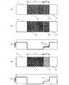
次いで、第2導電層106a上にレジスト膜を全面に塗布した後、図1(A)に示すマスクを用いて露光を行う。ここでは、膜厚1.5μmのレジスト膜を塗布し、露光は、解像度が1.5μmの露光機を用いる。露光に用いる光は、i線(波長365nm)であり、露光エネルギーは、20〜140mJ/cm2の範囲から選択する。また、i線に限定されず、i線とg線(波長436nm)とh線(波長405nm)とを混合させた光を露光に用いてもよい。
Next, after a resist film is applied over the entire surface of the second
図1(A)において、露光マスクは、Crなどの金属膜からなる遮光部401と、光強度低減機能を有する補助パターンとして、半透膜が設けられた部分(半透部とも呼ぶ)402とが基板400に設置されている。露光マスクの断面図において、遮光部401の幅はt1と示し、半透膜のみが設けられた部分402の幅はt2と示している。ここでは露光マスクの一部として半透膜を用いた例を示したが、回折格子パターンを用いてもよい。
In FIG. 1A, an exposure mask includes a
図1(A)に示す露光マスクを用いてレジスト膜の露光を行うと、非露光領域403aと露光領域403bが形成される。露光時には、光が遮光部401の回り込みや半透膜を通過することによって図1(A)に示す露光領域403bが形成される。
When the resist film is exposed using the exposure mask shown in FIG. 1A, a non-exposed region 403a and an exposed
そして、現像を行うと、露光領域403bが除去されて、図1(B)に示すように、膜厚の厚い領域と、該領域より膜厚の薄い領域を片側側部に有する左右非対称のレジストパターン107aが第2導電層106a上に得られる。左右非対称のレジストパターン107aにおいて、膜厚の薄い領域は、露光エネルギーを調節することでレジスト膜厚を調節することができる。
Then, when the development is performed, the exposed
次に、ドライエッチングにより第2導電層106a及び第1導電層105aのエッチングを行う。エッチングガスには、CF4、SF6、Cl2、O2を用いる。エッチング速度の向上にはECR(Electron Cyclotron Resonance)やICP(Inductively Coupled Plazma)などの高密度プラズマ源を用いたドライエッチング装置を用いる。なお、エッチング条件によっては、第2絶縁膜104もエッチングされて、部分的に膜厚が薄くなる。
Next, the second
こうして図1(C)で示すように、第2絶縁膜104上に第1導電層105b、第2導電層106bからなる導電積層パターンが形成される。エッチングによって、第1導電層105bは、両側壁が露出し、さらに第2の導電層106bと重ならない領域が露出される。なお、第1導電層105bの両側壁は、テーパー形状としてもよい。また、第2導電層106bの両側壁もテーパー形状としてもよい。
Thus, as shown in FIG. 1C, a conductive laminated pattern including the first
次いで、レジストパターン107bを除去した後、半導体層103への一導電型不純物の添加を行う。ここでは、一導電型不純物のイオンとしてリン(またはAs)を用い、nチャネル型TFTを作製する。サイドウォールを形成することなく、導電積層パターンを用いて自己整合的にLDD領域やソース領域やドレイン領域を形成することができる。
Next, after removing the resist
ゲート電極の外側に位置するソース領域及びドレイン領域を形成するためのドーピング処理を行う場合、導電積層パターンをマスクとして一導電型不純物のイオンを半導体層103に添加して高濃度の一導電型不純物領域110、111を形成すればよい。高濃度の一導電型不純物領域110、111の不純物濃度は1×10¹⁹〜5×10²¹/cm3(SIMS測定でのピーク値)とする。
In the case of performing a doping process for forming a source region and a drain region located outside the gate electrode, ions of one conductivity type impurity are added to the
また、ゲート電極とオーバーラップするLDD領域を形成するためのドーピング処理を行う場合、第2導電層と積層していない領域の第1導電層105bを通過させて、一導電型不純物のイオンを半導体層103に添加して低濃度の一導電型不純物領域109を形成すればよい。このドーピング条件として、第2導電層や第1導電層の膜厚にもよるが、この場合には50kV以上の加速電圧を要する。低濃度の一導電型不純物領域109の不純物領域の不純物濃度は、LDD領域を前提とすると1×10¹⁶〜5×10¹⁸/cm3(SIMS測定でのピーク値)とする。
In addition, in the case of performing a doping process for forming an LDD region overlapping with the gate electrode, ions of one conductivity type impurity are passed through the first
なお、ドーピングの順序は特に限定されず、先にソース領域及びドレイン領域を形成するためのドーピング処理を行った後、LDD領域を形成するためのドーピング処理を行ってもよい。また、LDD領域を形成するためのドーピング処理を行った後、ソース領域及びドレイン領域を形成するためのドーピング処理を行ってもよい。 Note that the order of doping is not particularly limited, and the doping process for forming the LDD region may be performed after the doping process for forming the source region and the drain region is performed first. In addition, after performing the doping process for forming the LDD region, the doping process for forming the source region and the drain region may be performed.
また、ここではドーピング処理を2回に分けて異なる濃度の不純物領域の形成を行う例を示したが、処理条件を調節して1回のドーピング処理で異なる濃度の不純物領域の形成を行ってもよい。 Although an example in which the doping process is divided into two times to form impurity regions having different concentrations has been described here, the impurity regions having different concentrations can be formed by one doping process by adjusting the processing conditions. Good.
また、ドーピングの前にレジストパターンを除去した例を示したが、ドーピング処理を行った後でレジストパターンを除去してもよい。レジストパターンを残したままドーピングを行うと、第2導電層の表面をレジストパターンで保護しながらドーピングを行うことができる。 Moreover, although the example which removed the resist pattern before doping was shown, you may remove a resist pattern after performing a doping process. When doping is performed with the resist pattern remaining, doping can be performed while protecting the surface of the second conductive layer with the resist pattern.
なお、上記ドーピング処理の際、第2導電層と重なる位置の半導体層は、一導電型不純物のイオンは添加されない領域となり、後に形成されるTFTのチャネル形成領域として機能する部分となる。 Note that in the doping process, the semiconductor layer in a position overlapping with the second conductive layer is a region to which ions of one conductivity type impurity are not added, and functions as a channel formation region of a TFT to be formed later.
また、導電積層パターン(第1導電層105b及び第2導電層106b)が半導体層103と交差する部位においてゲート電極となる。また、第1導電層105bのうち、第2の導電層106bと重ならない領域がLov領域の長さとなる。なお、Lov領域とは、ゲート電極と重なる低濃度不純物領域を指している。TFTを有する回路の種類や用途に合わせて、必要なLov領域の長さを決定し、その長さに基づいて露光マスクやエッチング条件を設定すればよい。
In addition, the conductive stacked pattern (the first
その後、窒化珪素を用いる第3絶縁膜112を形成する。そして、半導体層に添加された不純物元素の活性化および水素化を行う。
Thereafter, a third
次いで、透光性を有する無機材料(酸化シリコン、窒化シリコン、酸化窒化シリコンなど)または、低誘電率の有機化合物材料(感光性又は非感光性の有機樹脂材料)を用いて第4絶縁膜113を形成する。また、シロキサンを含む材料を用いて第4絶縁膜を形成してもよい。なお、シロキサンは、シリコン(Si)と酸素(O)との結合で骨格構造が構成される材料である。置換基として、少なくとも水素を含む有機基(例えばアルキル基、芳香族炭化水素)が用いられる。置換基として、フルオロ基を用いてもよい。または置換基として、少なくとも水素を含む有機基と、フルオロ基とを用いてもよい。
Next, the fourth insulating
次いで、第3のフォトマスクを用いてレジストからなるマスクを形成し、層間絶縁膜として機能する第3絶縁膜112、及び第4絶縁膜113、及びゲート絶縁膜として機能する第2絶縁膜104を選択的にエッチングしてコンタクトホールを形成する。そして、レジストからなるマスクを除去する。
Next, a resist mask is formed using a third photomask, and a third
次いで、第4絶縁膜113上にスパッタ法で金属積層膜を成膜した後、第4のフォトマスクを用いてレジストからなるマスクを形成し、選択的に金属積層膜をエッチングして、半導体層に接するソース電極114またはドレイン電極115を形成する。
Next, after a metal laminated film is formed over the fourth insulating
なお、TFTのソース電極114またはドレイン電極115と同時に接続電極(複数のTFT間を電気的に接続する電極)や端子電極(外部電源と接続するための電極)も第4絶縁膜113上に形成することができる。そして、レジストからなるマスクを除去する。なお、金属積層膜は、膜厚100nmのTi膜と、膜厚350nmのSiを微量に含むAl膜と、膜厚100nmのTi膜との3層積層とする。金属積層膜は、同じメタルスパッタ装置内で連続して形成することが好ましい。
A connection electrode (an electrode for electrically connecting a plurality of TFTs) and a terminal electrode (an electrode for connecting to an external power source) are also formed on the fourth insulating
以上の工程で、図1(D)に示したチャネル形成領域の片側のみに低濃度不純物領域を有するトップゲート型TFTが完成する。また、図1(D)にチャネル長Lを示す。 Through the above steps, a top gate TFT having a low concentration impurity region only on one side of the channel formation region shown in FIG. FIG. 1D shows the channel length L.
以上のように、本実施形態は、回折格子パターン或いは半透膜からなる光強度低減機能を有する補助パターンを設置したフォトマスクを用いて露光することによって、左右非対称な形状を有するレジストパターン107aを形成し、そのレジストパターンを利用して、左右非対称な形状を有するゲート電極を得ている。
As described above, in the present embodiment, the resist
従って、レジストパターン107aの膜厚の薄い部分の長さを調節することによって、自己整合的にLov領域の長さを調節することができる。
Accordingly, the length of the Lov region can be adjusted in a self-aligning manner by adjusting the length of the thin portion of the resist
例えば、バッファ回路に用いるnチャネル型TFTを形成する場合において、チャネル長Lを10μm、Lov領域の長さを1〜1.5μmとすることができる。この場合、ゲート電極幅、即ち導電積層パターンの幅(チャネル長方向の幅)は、11μm〜11.5μmとなる。 For example, when an n-channel TFT used for a buffer circuit is formed, the channel length L can be set to 10 μm, and the length of the Lov region can be set to 1 to 1.5 μm. In this case, the width of the gate electrode, that is, the width of the conductive laminated pattern (width in the channel length direction) is 11 μm to 11.5 μm.
本実施の形態では、nチャネル型TFTを用いて説明したが、n型不純物元素に代えてp型不純物元素を用いることによってpチャネル型TFTを形成することができる。 Although this embodiment mode is described using an n-channel TFT, a p-channel TFT can be formed by using a p-type impurity element instead of an n-type impurity element.
また、同一基板上にnチャネル型TFTとpチャネル型TFTとを形成することができ、これらのTFTを相補的に組み合わせることによってCMOS回路を構成することもできる。CMOS回路とは、少なくとも一つのnチャネル型TFTと一つのpチャネル型TFTとを有する回路(インバータ回路、NAND回路、AND回路、NOR回路、OR回路、シフトレジスタ回路、サンプリング回路、D/Aコンバータ回路、A/Dコンバータ回路、ラッチ回路、バッファ回路など)を指している。加えて、これらのCMOS回路を組み合わせることによってSRAMやDRAMなどのメモリ素子やその他の素子を基板上に構成することができる。また、さまざまな素子や回路を集積してCPUを基板上に構成することも可能である。 Further, an n-channel TFT and a p-channel TFT can be formed on the same substrate, and a CMOS circuit can be configured by combining these TFTs in a complementary manner. A CMOS circuit is a circuit having at least one n-channel TFT and one p-channel TFT (inverter circuit, NAND circuit, AND circuit, NOR circuit, OR circuit, shift register circuit, sampling circuit, D / A converter) Circuit, A / D converter circuit, latch circuit, buffer circuit, etc.). In addition, by combining these CMOS circuits, memory elements such as SRAM and DRAM and other elements can be formed on the substrate. It is also possible to configure a CPU on a substrate by integrating various elements and circuits.
また、露光マスクを変更するだけで、工程数を増やすことなく、同一基板上に上記構造(チャネル形成領域の片側のみにLov領域を有する構造)のトップゲート型TFTと、チャネル形成領域の両側にLov領域を有する構造であるトップゲート型TFTを形成することもできる。 Further, the top gate TFT having the above structure (a structure having a Lov region only on one side of the channel formation region) and the both sides of the channel formation region on the same substrate without changing the number of steps simply by changing the exposure mask. A top-gate TFT having a structure having a Lov region can also be formed.
また、本実施の形態では、シングルゲート構造のトップゲート型TFTを用いて説明したが、チャネル形成領域を複数有するマルチゲート構造であるトップゲート型TFTも形成することができる。また、露光マスクを変更するだけで、工程数を増やすことなく、同一基板上にシングルゲート構造のトップゲート型TFTと、マルチゲート構造であるトップゲート型TFTを形成することもできる。 Although this embodiment mode is described using a single-gate top-gate TFT, a top-gate TFT having a multi-gate structure having a plurality of channel formation regions can also be formed. In addition, a single-gate top gate TFT and a multi-gate top gate TFT can be formed on the same substrate without changing the number of steps simply by changing the exposure mask.
従って、工程数を増やすことなく、同一基板上に最適な構造のトランジスタを割り当てて様々な回路を構成することができる。 Therefore, various circuits can be configured by assigning transistors having an optimal structure on the same substrate without increasing the number of steps.
(実施の形態2)
本実施の形態では、実施の形態1で用いた回折格子パターン或いは半透膜からなる光強度低減機能を有する補助パターンを設置した露光マスクについて図2を用いて説明する。
(Embodiment 2)
In the present embodiment, an exposure mask provided with an auxiliary pattern having a light intensity reduction function made of the diffraction grating pattern or the semi-permeable film used in Embodiment 1 will be described with reference to FIG.
なお、図1(A)では露光マスクの断面図を示しており、同様に、図2においても遮光部の幅はt1と示し、補助パターンが設けられた部分の幅はt2と示している。 1A shows a cross-sectional view of the exposure mask. Similarly, in FIG. 2, the width of the light shielding portion is indicated by t1, and the width of the portion provided with the auxiliary pattern is indicated by t2.
補助パターンの具体例として、図2(A)と図2(B)に、露光装置の解像限界以下のラインおよびスペースから成るスリット部を有する回折格子パターンを備えた露光マスクの上面図の一部を示す。前記スリット部のスリットの方向は、スリット部203の様に主パターン(遮光部202)の方向と平行でも、スリット部207の様に主パターン(遮光部206)の方向と垂直でも構わない。尚、このフォトリソグラフィ工程で使用されるレジストはネガ型レジストが適用困難である為、当該ゲート電極形成用フォトマスクまたはレチクルのパターン構成は、ポジ型レジストを前提にしている。
As a specific example of the auxiliary pattern, FIGS. 2A and 2B are top views of an exposure mask provided with a diffraction grating pattern having a slit portion composed of lines and spaces below the resolution limit of the exposure apparatus. Indicates the part. The slit direction of the slit part may be parallel to the direction of the main pattern (light-shielding part 202) like the
前記ゲート電極形成用フォトマスクまたはレチクル201、205に露光光を照射した場合、遮光部202、206の光強度はほぼゼロであり、透光部204、208の光強度はほぼ100%である。一方、露光装置の解像限界以下のラインおよびスペースから成る回折格子パターンのスリット部203、207で構成される光強度低減機能を有する補助パターンの光強度は、10〜70%の範囲で調整可能となっており、その代表的光強度分布の例を図2(C)中の光強度分布209に示す。回折格子パターンに於ける前記スリット部203、207の光強度の調整は、スリット部203、207のピッチ及びスリット幅の調整により実現している。
When the gate electrode forming photomask or
また、補助パターンの具体例として、図2(D)に、露光光の光強度を低減する機能を有する半透膜からなる半透部を備えた露光マスクの上面図の一部を示す。半透膜としては、MoSiNの他に、MoSi、MoSiO、MoSiON、CrSiなどを用いることができる。半透部を備えた露光マスクを用いた露光法は、ハーフトーン露光法とも呼ばれる。 As a specific example of the auxiliary pattern, FIG. 2D shows a part of a top view of an exposure mask provided with a semi-transmissive portion made of a semi-transmissive film having a function of reducing the light intensity of exposure light. As the semipermeable membrane, in addition to MoSiN, MoSi, MoSiO, MoSiON, CrSi, or the like can be used. An exposure method using an exposure mask having a semi-transmissive portion is also called a halftone exposure method.
ゲート電極形成用フォトマスクまたはレチクル210に於けるゲート電極形成用マスクパターンの主パターンの領域が遮光部211で、光強度低減機能を有する補助パターンの領域が半透膜から成る半透光部212で、その外側の領域が透光部213である。
The main pattern region of the gate electrode formation mask pattern in the gate electrode formation photomask or
また、前記ゲート電極形成用フォトマスクまたはレチクル210に露光した場合、遮光部211の光強度はほぼゼロ、透光部213の光強度はほぼ100%であり、半透膜から成る半透光部212で構成される補助パターン領域の光強度は、10〜70%の範囲で調整可能となっており、その代表的光強度分布の例を図2(E)中の光強度分布214に示す。
In addition, when the gate electrode forming photomask or
また、本実施の形態は実施の形態1と自由に組み合わせることができる。 Further, this embodiment mode can be freely combined with Embodiment Mode 1.
(実施の形態3)
実施の形態1に示す導電積層パターンの形成は、特に限定されないが、ここでは、エッチング条件を途中で何度か変更して導電積層パターンの形成を行う例を図3に示す。
(Embodiment 3)
Although formation of the conductive laminated pattern shown in Embodiment 1 is not particularly limited, FIG. 3 shows an example in which the conductive laminated pattern is formed by changing the etching conditions several times in the middle.
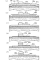
まず、実施の形態1と同様にして、第2導電層306a上にレジストパターン307aを形成する。図3(A)は、図1(B)に相当する。
First, in the same manner as in Embodiment Mode 1, a resist
なお、図3(A)において基板301上に第1絶縁膜(下地絶縁膜)302、半導体層303、第2絶縁膜(ゲート絶縁膜)304が形成され、その上に第1導電層305a、第2導電層306aが形成されている。
In FIG. 3A, a first insulating film (base insulating film) 302, a
次いで、図3(B)に示すように、レジストパターン307aをマスクとして用いて、第1のエッチング条件でエッチングを行い、第2導電層の一部を除去して第2導電層306bを形成する。なお、この段階での第2導電層306bは全面に形成されている。
Next, as shown in FIG. 3B, etching is performed under the first etching condition using the resist
次いで、図3(C)に示すように、第2のエッチング条件で、レジストパターンのトリミングを行い、レジストパターン307bを形成する。なお、第1のエッチングでレジストパターンがエッチングされてレジストパターン307bとほぼ同じ形状が得られる場合には、トリミングは特に行わなくともよい。また、トリミングを行わなくてもよいように、塗布で形成するレジスト膜厚を最初から薄くしてもよい。ここで言うトリミングとは、レジストパターンをエッチングしてレジストパターン寸法を加工することを指している。
Next, as shown in FIG. 3C, the resist pattern is trimmed under the second etching condition to form a resist
次いで、図3(D)に示すように、レジストパターン307bをマスクとして用いて第3のエッチング条件で、第2導電層の一部を除去して第1導電層の一部を露呈させる。この段階での第2導電層306cの断面形状は、L字形状となっている。
Next, as shown in FIG. 3D, a part of the second conductive layer is removed by exposing the part of the first conductive layer under the third etching condition using the resist
次いで、図3(E)に示すように、第2導電層306cをマスクとして用いて第4のエッチング条件で、第1導電層の一部を除去して第2絶縁膜304の一部を露呈させる。この段階で、第1導電層305bは、第2導電層306cと同じ幅を有している。この第4のエッチング条件まで第2絶縁膜は、第1導電層に覆われて保護されている。
Next, as shown in FIG. 3E, a part of the first insulating
次いで、図3(F)に示すように、第5のエッチング条件で異方性エッチングを行って第2導電層306dを形成する。この異方性エッチングにおいて、第1導電層と第2導電層のエッチングレートの差が大きいことが重要であり、第1導電層と第2導電層には異なる導電材料を用いることが好ましい。また、第5のエッチング条件を調整することによって、この異方性エッチングで第2絶縁膜が部分的に薄くならないようにすることもできる。
Next, as shown in FIG. 3F, anisotropic etching is performed under a fifth etching condition to form a second
こうして、エッチング条件を細かく変えて導電積層パターンの形成を行うことによって、導電積層パターンの形状のバラツキを抑えることができる。 Thus, by forming the conductive laminated pattern by finely changing the etching conditions, variations in the shape of the conductive laminated pattern can be suppressed.
以降の工程は、実施の形態1と同一であるのでここでは詳細な説明を省略する。 Since the subsequent steps are the same as those in the first embodiment, detailed description thereof is omitted here.
また、本実施の形態は実施の形態1または実施の形態2と自由に組み合わせることができる。 Further, this embodiment mode can be freely combined with Embodiment Mode 1 or Embodiment Mode 2.
(実施の形態4)
また、ここでは、露光マスクを変更するだけで、工程数を増やすことなく、同一基板上に上記構造(チャネル形成領域の片側のみにLov領域を有する構造)のトップゲート型TFTと、チャネル形成領域の両側にLov領域を有する構造であるトップゲート型TFTを形成する例を図4に示す。
(Embodiment 4)
Further, here, only by changing the exposure mask, without increasing the number of processes, the top gate TFT having the above structure (a structure having a Lov region only on one side of the channel formation region) on the same substrate, and the channel formation region FIG. 4 shows an example in which a top gate type TFT having a structure having Lov regions on both sides of the TFT is formed.
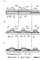
図4(A)において、基板500及び絶縁層508上に半導体層502、及び半導体層503が形成されている。半導体層502、及び半導体層503を覆うようにゲート絶縁層504、第1の導電膜505、及び第2の導電膜506が形成され、形状の異なるレジストパターン529、レジストパターン539、及びレジストパターン549が形成されている。これらのレジストパターンは、実施の形態1や実施の形態2に示す露光マスクを用いて形成することができる。
In FIG. 4A, a
レジストパターン529は両側になだらかな段差を有する形状であり、レジストパターン539は凸部が中央よりずれた位置にある形状であり、レジストパターン549は段差も凹凸もない形状(図9において左右対称の形状)である。
The resist
レジストパターン529、レジストパターン539、及びレジストパターン549を用いてエッチング処理によるパターニングを行い、第1のゲート電極層521、第2のゲート電極層522、第1のゲート電極層531、第2のゲート電極層532、第1の配線層541、及び第2の配線層542を形成する。これらの電極層の形成の際、ゲート絶縁層504も少しエッチングされてゲート絶縁層507が形成される。ゲート絶縁層504も少しエッチングすることで、導電膜のエッチング残渣をなくし、さらに後の工程で半導体層に達するコンタクトホールを形成する際、コンタクトホールを形成する箇所のゲート絶縁層の膜厚を薄くできるため、エッチング時間を短縮できる。
Patterning is performed by etching using the resist
第2のゲート電極層522、及び第2のゲート電極層532をマスクとして、半導体層502、及び半導体層503に一導電型を有する不純物元素を添加し、低濃度不純物領域524a、低濃度不純物領域524b、低濃度不純物領域534a、及び低濃度不純物領域534bを形成する(図4(B)参照。)。
Using the second
さらに、第1のゲート電極層521、第2のゲート電極層522、第1のゲート電極層531、第2のゲート電極層532をマスクとして、半導体層502、半導体層503に一導電型を有する不純物元素を添加し、高濃度不純物領域525a、高濃度不純物領域525b、低濃度不純物領域526a、低濃度不純物領域526b、高濃度不純物領域535a、高濃度不純物領域535b、低濃度不純物領域536を形成する。
Further, the
また、レジストパターン523、レジストパターン533、レジストパターン543を除去する。
Further, the resist
こうして、同一基板上に、第1のTFT部530と、第2のTFT部520と、配線部540とを形成することができる。第1のTFT部530には、チャネル形成領域の片側のみに低濃度不純物領域536を有するTFTが形成される。また、第2のTFT部520には、チャネル形成領域の両側に低濃度不純物領域526a、526bを有するTFTが作製される(図4(C)参照。)。また、配線部540には、端面の位置が一致している積層、即ち、第1の配線層541と第2の配線層542の積層が得られる。
Thus, the
加えて、同じレジストパターンを利用して、第1のTFT部530と同じ構造を形成して、同一基板上に容量とTFTとを形成することができる。ゲート絶縁層504を誘電体とし、低濃度不純物領域536と、第1のゲート電極層531及び第2のゲート電極層532とを一対の電極とする容量を形成することもできる。
In addition, by using the same resist pattern, the same structure as the
また、本実施の形態は実施の形態1、実施の形態2、または実施の形態3と自由に組み合わせることができる。 Further, this embodiment mode can be freely combined with Embodiment Mode 1, Embodiment Mode 2, or Embodiment Mode 3.
(実施の形態5)
本実施の形態では、アクティブマトリクス型の発光装置の構造について、図5、及び図6を用いて作製方法とともに、以下に説明する。
(Embodiment 5)
In this embodiment mode, a structure of an active matrix light-emitting device will be described below together with a manufacturing method with reference to FIGS.
まず、絶縁表面を有する基板610上に下地絶縁膜を形成する。基板610側を表示面として発光を取り出す場合、基板610としては、光透過性を有するガラス基板や石英基板を用いればよい。また、処理温度に耐えうる耐熱性を有する光透過性のプラスチック基板を用いてもよい。また、基板610側とは逆の面を表示面として発光を取り出す場合、前述の基板の他にシリコン基板、金属基板またはステンレス基板の表面に絶縁膜を形成したものを用いても良い。ここでは基板610としてガラス基板を用いる。なお、ガラス基板の屈折率は1.55前後である。 First, a base insulating film is formed over the substrate 610 having an insulating surface. In the case where light emission is extracted using the substrate 610 side as a display surface, a light-transmitting glass substrate or quartz substrate may be used as the substrate 610. Alternatively, a light-transmitting plastic substrate having heat resistance that can withstand the processing temperature may be used. In the case where light emission is extracted using a surface opposite to the substrate 610 side as a display surface, a substrate in which an insulating film is formed on the surface of a silicon substrate, a metal substrate, or a stainless steel substrate in addition to the above substrate may be used. Here, a glass substrate is used as the substrate 610. The refractive index of the glass substrate is around 1.55.
下地絶縁膜611としては、酸化シリコン膜、窒化シリコン膜または酸化窒化シリコン膜などの絶縁膜から成る下地膜を形成する。ここでは下地膜として単層構造を用いた例を示すが、前記絶縁膜を2層以上積層させた構造を用いても良い。なお、基板の凹凸や、基板からの不純物拡散が問題にならないのであれば、特に下地絶縁膜を形成しなくてもよい。
As the
次いで、下地絶縁膜上に半導体層を形成する。半導体層は、非晶質構造を有する半導体膜を公知の手段(スパッタ法、LPCVD法、またはプラズマCVD法等)により成膜した後、公知の結晶化処理(レーザー結晶化法、熱結晶化法、またはニッケルなどの触媒を用いた熱結晶化法等)を行って得られた結晶質半導体膜を第1のフォトマスクを用いて所望の形状にパターニングして、半導体層を形成する。なお、プラズマCVD法を用いれば、下地絶縁膜と、非晶質構造を有する半導体膜とを大気に触れることなく連続的に積層することができる。この半導体膜の厚さは25〜80nm(好ましくは30〜70nm)の厚さで形成する。結晶質半導体膜の材料に限定はないが、好ましくはシリコンまたはシリコンゲルマニウム(SiGe)合金などで形成すると良い。 Next, a semiconductor layer is formed over the base insulating film. The semiconductor layer is formed by forming a semiconductor film having an amorphous structure by a known means (sputtering method, LPCVD method, plasma CVD method, etc.), and then known crystallization treatment (laser crystallization method, thermal crystallization method). The crystalline semiconductor film obtained by performing a thermal crystallization method using a catalyst such as nickel or the like is patterned into a desired shape using a first photomask to form a semiconductor layer. Note that when a plasma CVD method is used, a base insulating film and a semiconductor film having an amorphous structure can be stacked successively without being exposed to the air. The semiconductor film is formed with a thickness of 25 to 80 nm (preferably 30 to 70 nm). There is no limitation on the material of the crystalline semiconductor film, but the crystalline semiconductor film is preferably formed of silicon or a silicon germanium (SiGe) alloy.
ここでは、非晶質構造を有する半導体膜を結晶化させる技術として、特開平8−78329号公報記載の技術を用いて結晶化させる。同公報記載の技術は、非晶質シリコン膜(アモルファスシリコン膜とも呼ばれる)に対して結晶化を助長する金属元素を選択的に添加し、加熱処理を行うことで添加領域を起点として広がる結晶構造を有する半導体膜を形成するものである。 Here, as a technique for crystallizing a semiconductor film having an amorphous structure, the technique described in JP-A-8-78329 is used for crystallization. The technology described in this publication is based on a crystal structure in which an amorphous silicon film (also referred to as an amorphous silicon film) is selectively added with a metal element that promotes crystallization, and heat treatment is performed to expand the added region as a starting point. The semiconductor film which has this is formed.
以下に結晶質半導体膜の形成方法の一例を詳細に説明する。 Hereinafter, an example of a method for forming a crystalline semiconductor film will be described in detail.
まず、非晶質構造を有す半導体膜の表面に、結晶化を促進する触媒作用のある金属元素(ここでは、ニッケル)を重量換算で1〜100ppm含む酢酸ニッケル溶液をスピナーで塗布してニッケル含有層を形成する。塗布によるニッケル含有層の形成方法以外の他の手段として、スパッタ法、蒸着法、またはプラズマ処理により極薄い膜を形成する手段を用いてもよい。また、ここでは、全面に塗布する例を示したが、マスクを形成して選択的にニッケル含有層を形成してもよい。 First, a nickel acetate solution containing a catalytic metal element (here, nickel) that promotes crystallization on a surface of an amorphous semiconductor film containing 1 to 100 ppm by weight is applied by a spinner. A containing layer is formed. As a means other than the method for forming the nickel-containing layer by coating, a means for forming an extremely thin film by sputtering, vapor deposition, or plasma treatment may be used. Although an example in which the coating is performed on the entire surface is shown here, a nickel-containing layer may be selectively formed by forming a mask.
次いで、加熱処理を行い、結晶化を行う。この場合、結晶化は半導体の結晶化を助長する金属元素が接した半導体膜の部分でシリサイドが形成され、それを核として結晶化が進行する。こうして、結晶構造を有す半導体膜が形成される。なお、結晶化後での半導体膜に含まれる酸素濃度は、5×10¹⁸/cm3以下とすることが望ましい。ここでは、脱水素化のための熱処理(450℃、1時間)の後、結晶化のための熱処理(550℃〜650℃で4〜24時間)を行う。また、強光の照射により結晶化を行う場合は、赤外光、可視光、または紫外光のいずれか一またはそれらの組み合わせを用いることが可能である。なお、必要であれば、強光を照射する前に非晶質構造を有する半導体膜に含有する水素を放出させる熱処理を行ってもよい。また、熱処理と強光の照射とを同時に行って結晶化を行ってもよい。生産性を考慮すると、結晶化は強光の照射により結晶化を行うことが望ましい。 Next, heat treatment is performed to perform crystallization. In this case, in crystallization, silicide is formed in a portion of the semiconductor film in contact with a metal element that promotes crystallization of the semiconductor, and crystallization proceeds using the silicide as a nucleus. Thus, a semiconductor film having a crystal structure is formed. Note that the concentration of oxygen contained in the semiconductor film after crystallization is preferably 5 × 10 18 / cm 3 or less. Here, after heat treatment for dehydrogenation (450 ° C., 1 hour), heat treatment for crystallization (550 to 650 ° C. for 4 to 24 hours) is performed. When crystallization is performed by irradiation with strong light, any one of infrared light, visible light, and ultraviolet light, or a combination thereof can be used. Note that if necessary, heat treatment for releasing hydrogen contained in the semiconductor film having an amorphous structure may be performed before irradiation with strong light. In addition, crystallization may be performed by simultaneously performing heat treatment and irradiation with strong light. In consideration of productivity, it is desirable to perform crystallization by irradiation with strong light.
このようにして得られる結晶質半導体膜には、金属元素(ここではニッケル)が残存している。それは膜中において一様に分布していないにしろ、平均的な濃度とすれば、1×10¹⁹/cm3を越える濃度で残存している。勿論、このような状態でもTFTをはじめ各種半導体素子を形成することが可能であるが、以降に示すゲッタリング方法で当該元素を除去する。 In the crystalline semiconductor film thus obtained, a metal element (here, nickel) remains. Although it is not uniformly distributed in the film, it remains at a concentration exceeding 1 × 10 19 / cm 3 in terms of an average concentration. Of course, various semiconductor elements including TFT can be formed even in such a state, but the element is removed by a gettering method described below.
ここで、レーザ光の照射を行う前に結晶化工程で形成される自然酸化膜を除去する。この自然酸化膜にはニッケルが高濃度に含まれているため、除去することが好ましい。 Here, the natural oxide film formed in the crystallization step is removed before the laser light irradiation. Since this natural oxide film contains nickel in high concentration, it is preferably removed.
次いで、結晶化率(膜の全体積における結晶成分の割合)を高め、結晶粒内に残される欠陥を補修するために、結晶質半導体膜に対してレーザ光を照射する。レーザ光を照射した場合、半導体膜に歪みやリッジが形成され、表面に薄い表面酸化膜(図示しない)が形成される。このレーザ光としてはパルス発振であるレーザ光源から射出される波長400nm以下のエキシマレーザ光や、YAGレーザの第2高調波、第3高調波を用いればよい。また、レーザ光としては連続発振が可能な固体レーザを用い、基本波の第2高調波〜第4高調波を用いてもよい。代表的には、Nd:YVO4レーザ(基本波1064nm)の第2高調波(532nm)や第3高調波(355nm)を適用すればよい。 Next, the crystalline semiconductor film is irradiated with laser light in order to increase the crystallization rate (the ratio of the crystal component in the total volume of the film) and repair defects remaining in the crystal grains. When laser light is irradiated, distortion and ridges are formed in the semiconductor film, and a thin surface oxide film (not shown) is formed on the surface. As this laser light, an excimer laser light having a wavelength of 400 nm or less emitted from a pulsed laser light source, or a second harmonic or a third harmonic of a YAG laser may be used. In addition, a solid-state laser capable of continuous oscillation may be used as the laser light, and the second to fourth harmonics of the fundamental wave may be used. Typically, a second harmonic (532 nm) or a third harmonic (355 nm) of an Nd: YVO 4 laser (fundamental wave 1064 nm) may be applied.
次いで、結晶質半導体膜の歪みを低減するための第1の熱処理(半導体膜が瞬間的に400〜1000℃程度にまで加熱される熱処理)を窒素雰囲気にて行い、平坦な半導体膜を得る。瞬間的に加熱する熱処理としては、強光を照射する熱処理、または加熱されたガス中に基板を投入し、数分放置した後に基板を取りだす熱処理によって加熱を行えばよい。また、この熱処理の条件によっては、歪みを低減すると同時に結晶粒内に残される欠陥を補修する、即ち結晶性の改善を行うことができる。また、この熱処理により、歪みを低減してニッケルが後のゲッタリング工程でゲッタリングされやすくなる。なお、この熱処理における温度が結晶化での温度よりも低い場合、シリコン膜が固相状態のまま、膜中にニッケルが移動することになる。 Next, first heat treatment (heat treatment in which the semiconductor film is instantaneously heated to about 400 to 1000 ° C.) for reducing distortion of the crystalline semiconductor film is performed in a nitrogen atmosphere to obtain a flat semiconductor film. As the heat treatment for instantaneously heating, heating may be performed by heat treatment for irradiating strong light, or heat treatment for putting a substrate into a heated gas and leaving it for several minutes, and then removing the substrate. Further, depending on the conditions of this heat treatment, it is possible to reduce the distortion and repair defects left in the crystal grains, that is, improve the crystallinity. This heat treatment also reduces the strain and makes it easier for the nickel to be gettered in a later gettering step. When the temperature in this heat treatment is lower than the temperature in crystallization, nickel moves into the film while the silicon film remains in a solid state.
次いで、結晶質半導体膜上方に希ガス元素を含む半導体膜を形成する。希ガス元素を含む半導体膜を形成する前にエッチングストッパーとなる酸化膜(バリア層と呼ばれる)を1〜10nmの膜厚で形成してもよい。バリア層は、半導体膜の歪みを低減するための熱処理で同時に形成してもよい。 Next, a semiconductor film containing a rare gas element is formed above the crystalline semiconductor film. An oxide film (referred to as a barrier layer) serving as an etching stopper may be formed with a thickness of 1 to 10 nm before forming a semiconductor film containing a rare gas element. The barrier layer may be formed at the same time by heat treatment for reducing distortion of the semiconductor film.
希ガス元素を含む半導体膜は、プラズマCVD法、またはスパッタ法にて形成し、膜厚10nm〜300nmのゲッタリングサイトを形成する。希ガス元素としてはヘリウム(He)、ネオン(Ne)、アルゴン(Ar)、クリプトン(Kr)、キセノン(Xe)から選ばれた一種または複数種を用いる。中でも安価なガスであるアルゴン(Ar)が好ましい。 The semiconductor film containing a rare gas element is formed by a plasma CVD method or a sputtering method to form a gettering site with a thickness of 10 nm to 300 nm. As the rare gas element, one or more selected from helium (He), neon (Ne), argon (Ar), krypton (Kr), and xenon (Xe) are used. Among them, argon (Ar) which is an inexpensive gas is preferable.
ここではPCVD法を用い、原料ガスとしてモノシランとアルゴンを用い、比率(モノシラン:アルゴン)を0.1:99.9〜1:9、好ましくは、1:99〜5:95に制御して成膜する。また、成膜時のRFパワー密度は、0.0017W/cm2〜0.48W/cm2とすることが望ましい。RFパワー密度は、高ければ高いほどゲッタリング効果が得られる膜質となり、加えて成膜速度が向上するため好ましい。また、成膜時の圧力は、1.333Pa(0.01Torr)〜133.322Pa(1Torr)とすることが望ましい。圧力は、高ければ高いほど成膜速度が向上するため好ましい。また、成膜温度は300℃〜500℃とすることが望ましい。こうして、膜中にアルゴンを1×1018/cm3〜1×1022/cm3、好ましくは、1×1020/cm3〜1×1021/cm3の濃度で含む半導体膜をプラズマCVD法で成膜することができる。上記半導体膜の成膜条件を上記範囲内で調節することで、成膜の際、バリア層に与えるダメージを低減することができ、半導体膜の膜厚のバラツキ発生や半導体膜に穴が形成されるという不良の発生を防ぐことができる。 Here, the PCVD method is used, monosilane and argon are used as source gases, and the ratio (monosilane: argon) is controlled to 0.1: 99.9 to 1: 9, preferably 1:99 to 5:95. Film. In addition, the RF power density during film formation is desirably 0.0017 W / cm 2 to 0.48 W / cm 2 . The higher the RF power density is, the higher the film quality with which the gettering effect can be obtained and, in addition, the film formation speed is improved, which is preferable. The pressure during film formation is preferably 1.333 Pa (0.01 Torr) to 133.322 Pa (1 Torr). The higher the pressure, the better the film formation speed. Further, it is desirable that the film forming temperature be 300 ° C. to 500 ° C. Thus, plasma CVD is performed on a semiconductor film containing argon at a concentration of 1 × 10 18 / cm 3 to 1 × 10 22 / cm 3 , preferably 1 × 10 20 / cm 3 to 1 × 10 21 / cm 3 in the film. The film can be formed by the method. By adjusting the film formation conditions of the semiconductor film within the above range, damage to the barrier layer during film formation can be reduced, and variations in the film thickness of the semiconductor film and holes are formed in the semiconductor film. It is possible to prevent the occurrence of defects.
膜中に不活性気体である希ガス元素イオンを含有させる意味は二つある。一つはダングリングボンドを形成することであり、他の一つは半導体膜に歪みを与えることである。半導体膜に歪みを与えるにはアルゴン(Ar)、クリプトン(Kr)、キセノン(Xe)などシリコンより原子半径の大きな元素を用いた時に顕著に得られる。また、膜中に希ガス元素を含有させることにより、格子歪だけでなく、不対結合手も形成させてゲッタリング作用に寄与する。 There are two meanings of including a rare gas element ion which is an inert gas in the film. One is to form dangling bonds, and the other is to strain the semiconductor film. Distortion of the semiconductor film is remarkably obtained when an element having a larger atomic radius than silicon, such as argon (Ar), krypton (Kr), or xenon (Xe), is used. Further, by containing a rare gas element in the film, not only lattice distortion but also dangling bonds are formed, contributing to the gettering action.
次いで、加熱処理を行い、結晶質半導体膜中における金属元素(ニッケル)の濃度を低減、あるいは除去するゲッタリングを行う。ゲッタリングを行う加熱処理としては、強光を照射する処理、炉を用いた熱処理、または加熱されたガスに基板を投入し、数分放置した後取りだすことによって加熱を行えばよい。ここでは、ゲッタリングを行うための第2の熱処理(半導体膜が瞬間的に400〜1000℃程度にまで加熱される熱処理)を窒素雰囲気にて行う。 Next, heat treatment is performed to perform gettering for reducing or removing the concentration of the metal element (nickel) in the crystalline semiconductor film. As the heat treatment for performing gettering, heat treatment may be performed by irradiating with strong light, heat treatment using a furnace, or by putting the substrate into a heated gas, leaving it for a few minutes, and taking it out. Here, second heat treatment for performing gettering (heat treatment in which the semiconductor film is instantaneously heated to about 400 to 1000 ° C.) is performed in a nitrogen atmosphere.
この第2の熱処理により、金属元素が希ガス元素を含む半導体膜に移動し、バリア層で覆われた結晶質半導体膜に含まれる金属元素の除去、または金属元素の濃度の低減が行われる。結晶質半導体膜に含まれる金属元素は、基板面と垂直な方向、且つ、希ガス元素を含む半導体膜に向かって移動する。 By this second heat treatment, the metal element moves to the semiconductor film containing the rare gas element, and the metal element contained in the crystalline semiconductor film covered with the barrier layer is removed or the concentration of the metal element is reduced. The metal element contained in the crystalline semiconductor film moves in a direction perpendicular to the substrate surface and toward the semiconductor film containing a rare gas element.
金属元素がゲッタリングの際に移動する距離は、結晶質半導体膜の厚さ程度の距離であればよく、比較的短時間でゲッタリングを完遂することができる。ここでは、ニッケルが結晶質半導体膜に偏析しないよう希ガス元素を含む半導体膜に移動させ、結晶質半導体膜に含まれるニッケルがほとんど存在しない、即ち膜中のニッケル濃度が1×10¹⁸/cm3以下、望ましくは1×1017/cm3以下になるように十分ゲッタリングする。なお、希ガス元素を含む半導体膜だけでなくバリア層もゲッタリングサイトとして機能する。 The distance that the metal element moves during gettering may be about the thickness of the crystalline semiconductor film, and the gettering can be completed in a relatively short time. Here, nickel is transferred to a semiconductor film containing a rare gas element so as not to segregate in the crystalline semiconductor film, and the nickel contained in the crystalline semiconductor film is almost absent, that is, the nickel concentration in the film is 1 × 10 18 / cm. Gettering is sufficiently performed so that it is 3 or less, preferably 1 × 10 17 / cm 3 or less. Note that not only a semiconductor film containing a rare gas element but also a barrier layer functions as a gettering site.
次いで、バリア層をエッチングストッパーとして、希ガス元素を含む半導体膜のみを選択的に除去する。希ガス元素を含む半導体膜のみを選択的にエッチングする方法としては、ClF3によるプラズマを用いないドライエッチング、或いはヒドラジンや、テトラメチルアンモニウムハイドロオキサイド(化学式 (CH3)4NOH)(略称TMAH)を含む水溶液などアルカリ溶液によるウエットエッチングで行うことができる。なお、ここでのエッチングで結晶質半導体膜にピンホールが形成されるのを防止するため、オーバーエッチング時間を少なめにする。 Next, only the semiconductor film containing a rare gas element is selectively removed using the barrier layer as an etching stopper. As a method of selectively etching only a semiconductor film containing a rare gas element, dry etching without using plasma with ClF 3 , hydrazine, tetramethylammonium hydroxide (chemical formula (CH 3 ) 4 NOH) (abbreviation TMAH) It can be performed by wet etching with an alkaline solution such as an aqueous solution containing. Note that in order to prevent pinholes from being formed in the crystalline semiconductor film by this etching, the overetching time is reduced.
次いで、フッ酸を含むエッチャントによりバリア層を除去する。 Next, the barrier layer is removed with an etchant containing hydrofluoric acid.
また、結晶質半導体膜の歪みを低減するための第1の熱処理が終わった後、Fなどの不純物を除去するため、フラッシュ物質を使用してフラッシングする処理を行ってもよい。例えば、PCVD装置を用いて、モノシランをフラッシュ物質として用い、ガス流量8〜10SLMをチャンバーに5〜20分間、好ましくは10分〜15分間導入し続けることで基板表面のフラッシングする処理(シランフラッシュとも呼ぶ)を行う。なお、1SLMは1000sccm、即ち、0.06m3/hである。また、PCVD装置を用いれば、フラッシングする処理と希ガス元素を含む半導体膜の形成を連続的に行えるため、好ましい。 Further, after the first heat treatment for reducing the distortion of the crystalline semiconductor film is completed, a flushing process may be performed using a flash substance in order to remove impurities such as F. For example, using a PCVD apparatus, monosilane is used as a flash substance, and a gas flow rate of 8 to 10 SLM is continuously introduced into the chamber for 5 to 20 minutes, preferably 10 to 15 minutes, and the substrate surface is flushed (also called silane flash). Call). Note that 1 SLM is 1000 sccm, that is, 0.06 m 3 / h. In addition, it is preferable to use a PCVD apparatus because a flushing process and a semiconductor film containing a rare gas element can be continuously formed.
以上の工程で、良好な結晶質半導体膜を得ることができる。 Through the above steps, a good crystalline semiconductor film can be obtained.
結晶質半導体膜を第1のフォトマスクを用いて所望の形状にパターニングした後、レジストマスクを除去する。次いで、必要があればTFTのしきい値を制御するために、微量な不純物元素(ボロンまたはリン)のドーピングを半導体層に対して行う。ここでは、ジボラン(B2H6)を質量分離しないでプラズマ励起したイオンドープ法を用いる。 After the crystalline semiconductor film is patterned into a desired shape using a first photomask, the resist mask is removed. Next, if necessary, a small amount of impurity element (boron or phosphorus) is doped into the semiconductor layer in order to control the threshold value of the TFT. Here, an ion doping method in which diborane (B 2 H 6 ) is plasma-excited without mass separation is used.
次いで、フッ酸を含むエッチャントで半導体層表面の酸化膜を除去すると同時に半導体層の表面を洗浄する。 Next, the oxide film on the surface of the semiconductor layer is removed with an etchant containing hydrofluoric acid, and at the same time, the surface of the semiconductor layer is washed.
そして、半導体層を覆う絶縁膜を形成する。絶縁膜はプラズマCVD法またはスパッタ法を用い、厚さを1〜200nmとする。好ましくは10nm〜50nmと薄くしてシリコンを含む絶縁膜の単層または積層構造で形成した後にマイクロ波によるプラズマを用いた表面窒化処理を行う。絶縁膜は、後に形成されるTFTのゲート絶縁膜として機能する。 Then, an insulating film covering the semiconductor layer is formed. The insulating film is formed by plasma CVD or sputtering and has a thickness of 1 to 200 nm. It is preferably formed as a single layer or a laminated structure of an insulating film containing silicon by thinning to 10 nm to 50 nm, and then surface nitriding treatment using plasma by microwave is performed. The insulating film functions as a gate insulating film of a TFT formed later.
次いで、絶縁膜上に膜厚20〜100nmの第1の導電膜と、膜厚100〜400nmの第2の導電膜とを積層形成する。本実施の形態では、絶縁膜613上に膜厚50nmの窒化タンタル膜、膜厚370nmのタングステン膜を順次積層し、実施の形態1に示したパターニングを行って各ゲート電極及び各配線を形成する。本実施の形態では、回折格子パターン或いは半透膜からなる光強度低減機能を有する補助パターンを設置したフォトマスクまたはレチクルを用いて、各ゲート電極及び各配線を形成する。
Next, a first conductive film with a thickness of 20 to 100 nm and a second conductive film with a thickness of 100 to 400 nm are stacked over the insulating film. In this embodiment mode, a 50-nm-thick tantalum nitride film and a 370-nm-thickness tungsten film are sequentially stacked over the insulating
なお、ここでは導電膜をTaN膜とW膜との積層としたが、特に限定されず、Ta、W、Ti、Mo、Al、Cuから選ばれた元素、または前記元素を主成分とする合金材料若しくは化合物材料の積層で形成してもよい。また、リン等の不純物元素をドーピングした多結晶シリコン膜に代表される半導体膜を用いてもよい。また、2層構造に限定されず、例えば、膜厚50nmのタングステン膜、膜厚500nmのアルミニウムとシリコンの合金(Al−Si)膜、膜厚30nmの窒化チタン膜を順次積層した3層構造としてもよい。 Here, the conductive film is a laminate of a TaN film and a W film, but is not particularly limited, and an element selected from Ta, W, Ti, Mo, Al, and Cu, or an alloy containing the above element as a main component You may form by lamination | stacking of material or a compound material. Alternatively, a semiconductor film typified by a polycrystalline silicon film doped with an impurity element such as phosphorus may be used. Further, the present invention is not limited to the two-layer structure. For example, a three-layer structure in which a 50 nm-thickness tungsten film, a 500 nm-thickness aluminum and silicon alloy (Al-Si) film, and a 30 nm-thickness titanium nitride film are sequentially stacked. Also good.
上記第1の導電膜及び第2の導電膜のエッチング(第1のエッチング処理および第2のエッチング処理)にはICP(Inductively Coupled Plasma:誘導結合型プラズマ)エッチング法を用いると良い。ICPエッチング法を用い、エッチング条件(コイル型の電極に印加される電力量、基板側の電極に印加される電力量、基板側の電極温度等)を適宜調節することによって所望の形状に膜をエッチングすることができる。 An ICP (Inductively Coupled Plasma) etching method may be used for etching the first conductive film and the second conductive film (first etching process and second etching process). Using the ICP etching method, the film is formed into a desired shape by appropriately adjusting the etching conditions (the amount of power applied to the coil-type electrode, the amount of power applied to the electrode on the substrate side, the electrode temperature on the substrate side, etc.). It can be etched.
次いで、n型を付与する不純物元素を半導体層に添加するため、ゲート電極をマスクとして全面にドーピングする第1のドーピング処理を行う。第1のドーピング処理はイオンドープ法、もしくはイオン注入法で行えば良い。イオンドープ法の条件はドーズ量を1.5×10¹³atoms/cm2とし、加速電圧を50〜100kVとして行う。n型を付与する不純物元素として、典型的にはリン(P)または砒素(As)を用いる。 Next, in order to add an impurity element imparting n-type conductivity to the semiconductor layer, a first doping process is performed in which the entire surface is doped using the gate electrode as a mask. The first doping process may be performed by an ion doping method or an ion implantation method. The conditions of the ion doping method are a dose amount of 1.5 × 10 13 atoms / cm 2 and an acceleration voltage of 50 to 100 kV. Typically, phosphorus (P) or arsenic (As) is used as the impurity element imparting n-type conductivity.
次いで、レジストからなるマスクを形成した後、半導体にn型を付与する不純物元素を高濃度にドープするための第2のドーピング工程を行う。マスクは、画素部のpチャネル型TFTを形成する半導体層のチャネル形成領域及びその周辺の領域と、画素部のnチャネル型TFTの一部と、駆動回路部のpチャネル型TFTを形成する半導体層のチャネル形成領域及びその周辺の領域と、を保護するために設ける。 Next, after forming a mask made of resist, a second doping step is performed for doping the semiconductor with an impurity element imparting n-type at a high concentration. The mask includes a channel formation region of the semiconductor layer forming the p-channel TFT in the pixel portion and its peripheral region, a part of the n-channel TFT in the pixel portion, and a semiconductor forming the p-channel TFT in the driver circuit portion. It is provided to protect the channel formation region of the layer and the surrounding region.
第2のドーピング工程におけるイオンドープ法の条件はドーズ量を1×10¹³〜5×10¹⁵/cm2とし、加速電圧を60〜100kVとして行う。 The conditions of the ion doping method in the second doping step are a dose amount of 1 × 10 13 to 5 × 10 15 / cm 2 and an acceleration voltage of 60 to 100 kV.
次いで、マスクを除去した後、新たにレジストからなるマスクを形成し、半導体にp型を付与する不純物元素(代表的にはボロン)を高濃度にドープするための第3のドーピング工程を行う。マスクは、画素部のnチャネル型TFTを形成する半導体層のチャネル形成領域及びその周辺の領域と、駆動回路部のnチャネル型TFTを形成する半導体層のチャネル形成領域及びその周辺の領域と、を保護するために設ける。 Next, after removing the mask, a new mask made of resist is formed, and a third doping step for doping the semiconductor with p-type impurity element (typically boron) at a high concentration is performed. The mask includes a channel formation region of the semiconductor layer that forms the n-channel TFT in the pixel portion and a peripheral region thereof, a channel formation region of the semiconductor layer that forms the n-channel TFT of the driver circuit portion, and a peripheral region thereof, Provided to protect
この後、レジストマスクを除去する。以上までの工程でそれぞれの半導体層にn型またはp型の導電型を有する不純物領域が形成される。 Thereafter, the resist mask is removed. Through the above steps, impurity regions having n-type or p-type conductivity are formed in each semiconductor layer.
次いで、スパッタ法、LPCVD法、またはプラズマCVD法等を用いて、水素を含む絶縁膜を成膜した後、半導体層に添加された不純物元素の活性化および水素化を行う。水素を含む絶縁膜は、PCVD法により得られる窒化酸化珪素膜(SiNO膜)を用いる。ここでは、水素を含む絶縁膜の膜厚は、50nm〜200nmとする。加えて、結晶化を助長する金属元素、代表的にはニッケルを用いて半導体膜を結晶化させている場合、活性化と同時にチャネル形成領域におけるニッケルの低減を行うゲッタリングをも行うことができる。なお、水素を含む絶縁膜は、層間絶縁膜の1層目であり、酸化珪素を含んでいる。 Next, after an insulating film containing hydrogen is formed by a sputtering method, an LPCVD method, a plasma CVD method, or the like, the impurity element added to the semiconductor layer is activated and hydrogenated. As the insulating film containing hydrogen, a silicon nitride oxide film (SiNO film) obtained by a PCVD method is used. Here, the thickness of the insulating film containing hydrogen is 50 nm to 200 nm. In addition, when the semiconductor film is crystallized using a metal element that promotes crystallization, typically nickel, gettering that reduces nickel in the channel formation region at the same time as activation can be performed. . Note that the insulating film containing hydrogen is the first layer of the interlayer insulating film and contains silicon oxide.
次いで、スパッタ法、LPCVD法、またはプラズマCVD法等を用いて層間絶縁膜の2層目となる無機絶縁膜を形成する。無機絶縁膜としては、酸化シリコン膜、窒化シリコン膜または酸化窒化シリコン膜などの絶縁膜の単層または積層を用いる。ここでは無機絶縁膜の膜厚は600nm〜800nmとする。 Next, an inorganic insulating film serving as a second layer of the interlayer insulating film is formed by a sputtering method, an LPCVD method, a plasma CVD method, or the like. As the inorganic insulating film, a single layer or a stacked layer of insulating films such as a silicon oxide film, a silicon nitride film, or a silicon oxynitride film is used. Here, the thickness of the inorganic insulating film is 600 nm to 800 nm.
次いで、フォトマスクを用いてレジストからなるマスクを形成し、絶縁膜を選択的にエッチングしてコンタクトホールを形成する。そして、レジストからなるマスクを除去する。 Next, a resist mask is formed using a photomask, and the insulating film is selectively etched to form contact holes. Then, the resist mask is removed.
次いで、スパッタ法により金属膜を積層した後、フォトマスクを用いてレジストからなるマスクを形成し、選択的に金属積層膜をエッチングして、TFTのソース電極またはドレイン電極として機能する電極を形成する。なお、金属積層膜は、同じメタルスパッタ装置内で連続して形成する。そして、レジストからなるマスクを除去する。 Next, after a metal film is stacked by sputtering, a mask made of a resist is formed using a photomask, and the metal stacked film is selectively etched to form an electrode that functions as a source electrode or a drain electrode of the TFT. . The metal laminated film is continuously formed in the same metal sputtering apparatus. Then, the resist mask is removed.
以上の工程で、同一基板上にポリシリコン膜を活性層とするトップゲート型のTFT636、637、638、639が作製できる。
Through the above steps,
なお、画素部に配置されるTFT638は、一つのTFTに複数のチャネル形成領域を有するnチャネル型TFTである。TFT638は、ダブルゲート型のTFTである。また、画素部には、後に形成される発光素子と電気的に接続するTFT639が設けられる。ここでは、オフ電流低減のため、TFT639として、ダブルゲート型のpチャネル型TFTを示したが、特に限定されず、シングルゲート型のTFTとしてもよい。
Note that the
また、駆動回路部に配置されるTFT636は、ゲート電極と重なる低濃度不純物領域(Lov領域とも呼ぶ)をドレイン側のみに備えたnチャネル型TFTである。また、TFT637は、ゲート電極と重なる低濃度不純物領域(Lov領域)をソース側とドレイン側の両方に備えたpチャネル型TFTである。いずれもシングルゲート構造のTFTである。駆動回路部においては、TFT636とTFT637を相補的に接続することでCMOS回路を構成し、様々な種類の回路を実現することができる。また、必要であれば、マルチゲート構造のTFTとすることができる。
The
次いで、第1の電極623、即ち、有機発光素子の陽極(或いは陰極)を形成する。第1の電極623として、仕事関数の大きい材料、例えば、Ni、W、Cr、Pt、Zn、Sn、InまたはMoから選ばれた元素、または前記元素を主成分とする合金材料、例えばTiN、TiSiXNY、WSiX、WNX、WSiXNY、NbNを用いて、単層膜またはそれらの積層膜を総膜厚100nm〜800nmの範囲で用いればよい。
Next, the
具体的には第1の電極623として、透光性を有する導電性材料からなる透明導電膜を用いればよく、酸化タングステンを含むインジウム酸化物、酸化タングステンを含むインジウム亜鉛酸化物、酸化チタンを含むインジウム酸化物、酸化チタンを含むインジウム錫酸化物などを用いることができる。勿論、インジウム錫酸化物(ITO)、インジウム亜鉛酸化物(IZO)、酸化ケイ素を添加したインジウム錫酸化物(ITSO)なども用いることができる。
Specifically, a transparent conductive film formed using a light-transmitting conductive material may be used as the
また、各透光性を有する導電性材料の、組成比例を述べる。酸化タングステンを含むインジウム酸化物の組成比は、酸化タングステン1.0wt%、インジウム酸化物99.0wt%とすればよい。酸化タングステンを含むインジウム亜鉛酸化物の組成比は、酸化タングステン1.0wt%、酸化亜鉛0.5wt%、インジウム酸化物98.5wt%とすればよい。酸化チタンを含むインジウム酸化物は、酸化チタン1.0wt%〜5.0wt%、インジウム酸化物99.0wt%〜95.0wt%とすればよい。インジウム錫酸化物(ITO)の組成比は、酸化錫10.0wt%、インジウム酸化物90.0wt%とすればよい。インジウム亜鉛酸化物(IZO)の組成比は、酸化亜鉛10.7wt%、インジウム酸化物89.3wt%とすればよい。酸化チタンを含むインジウム錫酸化物の組成比は、酸化チタン5.0wt%、酸化錫10.0wt%、インジウム酸化物85.0wt%とすればよい。上記組成比は例であり、適宜その組成比の割合は設定すればよい。 In addition, compositional proportions of each light-transmitting conductive material will be described. The composition ratio of indium oxide containing tungsten oxide may be 1.0 wt% tungsten oxide and 99.0 wt% indium oxide. The composition ratio of indium zinc oxide containing tungsten oxide may be 1.0 wt% tungsten oxide, 0.5 wt% zinc oxide, and 98.5 wt% indium oxide. The indium oxide containing titanium oxide may be 1.0 wt% to 5.0 wt% titanium oxide and 99.0 wt% to 95.0 wt% indium oxide. The composition ratio of indium tin oxide (ITO) may be 10.0 wt% tin oxide and 90.0 wt% indium oxide. The composition ratio of indium zinc oxide (IZO) may be 10.7 wt% zinc oxide and 89.3 wt% indium oxide. The composition ratio of indium tin oxide containing titanium oxide may be 5.0 wt% titanium oxide, 10.0 wt% tin oxide, and 85.0 wt% indium oxide. The above composition ratio is an example, and the ratio of the composition ratio may be set as appropriate.
次いで、塗布法により得られる絶縁膜(例えば、有機樹脂膜)をパターニングして、第1の電極623の端部を覆う絶縁物629(バンク、隔壁、障壁、土手などと呼ばれる)を形成する。なお、絶縁物629の形成は、マスクを用いるパターニングに限定されず、感光性材料を用いて露光と現像のみで形成してもよい。
Next, an insulating film (e.g., an organic resin film) obtained by a coating method is patterned to form an insulator 629 (referred to as a bank, a partition, a barrier, a bank, or the like) that covers an end portion of the
次いで、有機化合物を含む層624を、蒸着法または塗布法を用いて形成する。
Next, a
有機化合物を含む層624は、積層であり、有機化合物を含む層624の一層としてバッファ層を用いてもよい。バッファ層は、有機化合物と無機化合物とを含む複合材料であり、前記無機化合物は、前記有機化合物に対して電子受容性を示す。前記無機化合物は、酸化チタン、酸化ジルコニウム、酸化ハフニウム、酸化バナジウム、酸化ニオブ、酸化タンタル、酸化クロム、酸化モリブデン、酸化タングステン、酸化マンガン、および酸化レニウムからなる群より選ばれるいずれか一または複数である。バッファ層は、ホール輸送性を有する有機化合物と、無機化合物とを含む複合材料である。
The
例えば、第1の電極623と第2の電極の間には有機化合物を含む積層(バッファ層と有機化合物層の積層)を設けることが好ましい。バッファ層は、金属酸化物(酸化モリブデン、酸化タングステン、酸化レニウムなど)と有機化合物(ホール輸送性を有する材料(例えば4,4’−ビス[N−(3−メチルフェニル)−N−フェニルアミノ]ビフェニル(略称:TPD)、4,4’−ビス[N−(1−ナフチル)−N−フェニルアミノ]ビフェニル(略称:α−NPD)、4,4’−ビス{N−[4−(N,N−ジ−m−トリルアミノ)フェニル]−N−フェニルアミノ}ビフェニル(略称:DNTPD)など))とを含む複合層である。また、有機化合物層は、例えば、トリス(8−キノリノラト)アルミニウム(略称:Alq3)や、トリス(4−メチル−8−キノリノラト)アルミニウム(略称:Almq3)や、α−NPDなどを用いることができる。また、有機化合物層は、ドーパント材料を含ませてもよく、例えば、N,N’−ジメチルキナクリドン(略称:DMQd)や、クマリン6や、ルブレンなどを用いることができる。第1の電極と第2の電極の間に設けられる有機化合物を含む積層は、抵抗加熱法などの蒸着法によって形成すればよい。
For example, a stack containing an organic compound (a stack of a buffer layer and an organic compound layer) is preferably provided between the
バッファ層の膜厚を調節することによって、第1の電極と有機化合物層との距離を制御し、発光効率を高めることができる。バッファ層の膜厚を調節することによって、各発光素子からの発光色がきれいに表示された優れた映像を表示でき、低消費電力化された発光装置を実現することができる。 By adjusting the thickness of the buffer layer, the distance between the first electrode and the organic compound layer can be controlled to increase the light emission efficiency. By adjusting the thickness of the buffer layer, it is possible to display an excellent image in which the emission color from each light emitting element is clearly displayed, and to realize a light emitting device with low power consumption.
次いで、第2の電極625、即ち、有機発光素子の陰極(或いは陽極)を形成する。第2の電極625としては、MgAg、MgIn、AlLiなどの合金、または透明導電膜(ITOなど)を用いる。
Next, a
次いで、蒸着法またはスパッタ法により保護層626を形成する。保護層626は、第2の電極625を保護する。保護層626を通過させて発光素子の発光を取り出す場合、透明な材料とすることが好ましい。なお、必要でなければ保護層626は設けなくともよい。
Next, the
次いで、封止基板633をシール材628で貼り合わせて発光素子を封止する。即ち、発光表示装置は、表示領域の外周をシール材で囲み、一対の基板で封止される。TFTの層間絶縁膜は、基板全面に設けられているため、シール材のパターンが層間絶縁膜の外周縁よりも内側に描画された場合、シール材のパターンの外側に位置する層間絶縁膜の一部から水分や不純物が浸入する恐れがある。従って、TFTの層間絶縁膜として用いる絶縁膜の外周は、シール材のパターンの内側、好ましくは、シール材パターンと重なるようにして絶縁膜の端部をシール材が覆うようにする。なお、シール材628で囲まれた領域には充填材627を充填する。或いは、シール材628で囲まれた領域には乾燥した不活性ガスを充填する。
Next, the sealing
最後にFPC632を異方性導電膜631により公知の方法で端子電極と貼りつける。この段階での断面図を図5に示す。なお、端子電極は、第1の電極623と同じ工程で得られる透明導電膜を最上層に用いることが好ましく、ゲート配線と同時に形成された端子電極上に形成する。
Finally, the FPC 632 is attached to the terminal electrode by an anisotropic
また、図6は、画素部の上面図を示しており、図6中の鎖線E−Fで切断した断面が、図5における画素部のpチャネル型TFT639の断面構造に対応している。また、図6中の鎖線M−Lで切断した断面が、図5における画素部のnチャネル型TFT638の断面構造に対応している。なお、図6中の680で示した実線は、絶縁物629の周縁を示している。ただし、図6においては、第2導電層のみを図示しており、第1導電層は図示していない。
6 shows a top view of the pixel portion, and a cross section taken along a chain line EF in FIG. 6 corresponds to the cross-sectional structure of the p-
以上の工程によって、画素部と駆動回路と端子部とを同一基板上に形成することができる。 Through the above steps, the pixel portion, the driver circuit, and the terminal portion can be formed over the same substrate.
本実施の形態において、オフ電流低減のために画素部のTFTをダブルゲート構造とし、駆動回路のnチャネル型TFTに本実施の形態1のTFTを用いている。 In this embodiment mode, the TFT in the pixel portion has a double gate structure in order to reduce off-state current, and the TFT in Embodiment Mode 1 is used as an n-channel TFT in a driver circuit.
また、発光装置において、発光装置の発光表示面は、一面または両面であってもよい。第1の電極623と第2の電極625とを透明導電膜で形成した場合、発光素子の光は、基板610及び封止基板633を通過して両側に取り出される。この場合、封止基板633や充填材627は透明な材料を用いることが好ましい。
In the light emitting device, the light emitting display surface of the light emitting device may be one surface or both surfaces. In the case where the
また、第2の電極625を金属膜で形成し、第1の電極623を透明導電膜で形成した場合、発光素子の光は、基板610のみを通過して一方に取り出される構造、即ちボトムエミッション型となる。この場合、封止基板633や充填材627は透明な材料を用いなくともよい。
In the case where the
また、第1の電極623を金属膜で形成し、第2の電極625を透明導電膜で形成した場合、発光素子の光は、封止基板633のみを通過して一方に取り出される構造、即ちトップエミッション型となる。この場合、基板610は透明な材料を用いなくともよい。
In the case where the
また、第1の電極623及び第2の電極625は仕事関数を考慮して材料を選択する必要がある。但し第1の電極及び第2の電極は、画素構成によりいずれも陽極、又は陰極となりうる。駆動用TFTの極性がpチャネル型である場合、第1の電極を陽極、第2の電極を陰極とするとよい。また、駆動用TFTの極性がNチャネル型である場合、第1の電極を陰極、第2の電極を陽極とすると好ましい。
In addition, materials for the
また、フルカラー表示する場合、本実施の形態の画素部における等価回路図を図7に示す。図7中のTFT638が図5のスイッチングTFT638に対応しており、TFT639が電流制御用TFT639に対応している。赤色を表示する画素は、電流制御用TFT639のドレイン領域に赤色を発光するOLED703Rが接続され、ソース領域にはアノード側電源線(R)706Rが設けられている。また、OLED703Rには、カソード側電源線700が設けられている。また、緑色を表示する画素は、電流制御用TFTのドレイン領域に緑色を発光するOLED703Gが接続され、ソース領域にはアノード側電源線(G)706Gが設けられている。また、青色を表示する画素は、電流制御用TFTのドレイン領域に青色を発光するOLED703Bが接続され、ソース領域にはアノード側電源線(B)706Bが設けられている。それぞれ色の異なる画素にはEL材料に応じて異なる電圧をそれぞれ印加する。
FIG. 7 shows an equivalent circuit diagram in the pixel portion of this embodiment in the case of full color display. The
また、発光装置において、画面表示の駆動方法は特に限定されず、例えば、点順次駆動方法や線順次駆動方法や面順次駆動方法などを用いればよい。代表的には、線順次駆動方法とし、時分割階調駆動方法や面積階調駆動方法を適宜用いればよい。また、発光装置のソース線に入力する映像信号は、アナログ信号であってもよいし、デジタル信号であってもよく、適宜、映像信号に合わせて駆動回路などを設計すればよい。 In the light emitting device, a driving method for screen display is not particularly limited, and for example, a dot sequential driving method, a line sequential driving method, a surface sequential driving method, or the like may be used. Typically, a line sequential driving method is used, and a time-division gray scale driving method or an area gray scale driving method may be used as appropriate. The video signal input to the source line of the light-emitting device may be an analog signal or a digital signal, and a drive circuit or the like may be designed in accordance with the video signal as appropriate.
さらに、ビデオ信号がデジタルの発光装置において、画素に入力されるビデオ信号が定電圧(CV)のものと、定電流(CC)のものとがある。ビデオ信号が定電圧のもの(CV)には、発光素子に印加される信号の電圧が一定のもの(CVCV)と、発光素子に印加される信号の電流が一定のもの(CVCC)とがある。また、ビデオ信号が定電流のもの(CC)には、発光素子に印加される信号の電圧が一定のもの(CCCV)と、発光素子に印加される信号の電流が一定のもの(CCCC)とがある。 Further, in a light emitting device in which a video signal is digital, there are a video signal input to a pixel having a constant voltage (CV) and a constant current (CC). A video signal having a constant voltage (CV) includes a signal having a constant voltage applied to the light emitting element (CVCV) and a signal having a constant current applied to the light emitting element (CVCC). . In addition, when the video signal has a constant current (CC), the signal voltage applied to the light emitting element is constant (CCCV), and the signal applied to the light emitting element has a constant current (CCCC). There is.
また、発光装置において、静電破壊防止のための保護回路(保護ダイオードなど)を設けてもよい。 In the light emitting device, a protection circuit (such as a protection diode) for preventing electrostatic breakdown may be provided.
また、ここでは表示装置としてアクティブマトリクス型の発光装置の例を示したが、アクティブマトリクス型の液晶表示装置にも適用できる。 Although an example of an active matrix light-emitting device is described here as a display device, the present invention can also be applied to an active matrix liquid crystal display device.
また、本実施の形態は実施の形態1、実施の形態2、実施の形態3、または実施の形態4と自由に組み合わせることができる。 Further, this embodiment mode can be freely combined with Embodiment Mode 1, Embodiment Mode 2, Embodiment Mode 3, or Embodiment Mode 4.
(実施の形態6)
本実施の形態では、実施の形態5と結晶質半導体膜の形成方法が一部異なる例を示す。また、マルチゲート構造のTFTの作製を例に用いて図8に説明する。
(Embodiment 6)
In this embodiment, an example in which the method for forming a crystalline semiconductor film is partly different from that in Embodiment 5 is shown. In addition, FIG. 8 will be described with reference to an example of manufacturing a multi-gate TFT.
まず、実施の形態5と同様に絶縁表面を有する基板上に下地絶縁膜、非晶質構造を有する半導体膜を形成する。 First, as in Embodiment Mode 5, a base insulating film and a semiconductor film having an amorphous structure are formed over a substrate having an insulating surface.
次いで、実施の形態5と同様に非晶質構造を有す半導体膜の表面に、結晶化を促進する触媒作用のある金属元素(ここでは、ニッケル)を重量換算で1〜100ppm含む酢酸ニッケル溶液をスピナーで塗布してニッケル含有層を形成する。 Next, in the same manner as in the fifth embodiment, a nickel acetate solution containing 1 to 100 ppm by weight of a metal element (here, nickel) having a catalytic action for promoting crystallization on the surface of a semiconductor film having an amorphous structure. Is applied with a spinner to form a nickel-containing layer.
次いで、実施の形態5と同様に加熱処理を行い、結晶化を行う。ここでは、脱水素化のための熱処理(450℃、1時間)の後、結晶化のための熱処理(550℃〜650℃で4〜24時間)を行って結晶質半導体膜を得る。 Next, heat treatment is performed in the same manner as in Embodiment 5 to perform crystallization. Here, after the heat treatment for dehydrogenation (450 ° C., 1 hour), the heat treatment for crystallization (550 ° C. to 650 ° C. for 4 to 24 hours) is performed to obtain a crystalline semiconductor film.
次いで、実施の形態5と同様に、結晶化率を高め、結晶粒内に残される欠陥を補修するために、結晶質半導体膜に対してレーザ光を照射する。 Next, as in the fifth embodiment, the crystalline semiconductor film is irradiated with laser light in order to increase the crystallization rate and repair defects remaining in the crystal grains.
次いで、フォトマスクを用いて結晶質半導体膜のパターニングを行う。ここでは、島状の半導体層801を形成するとともに、その島状の半導体層に開口803を数カ所形成する。
Next, the crystalline semiconductor film is patterned using a photomask. Here, island-shaped semiconductor layers 801 are formed, and
次いで、結晶質半導体膜の歪みを低減するための第1の熱処理(半導体膜が瞬間的に400〜1000℃程度にまで加熱される熱処理)を窒素雰囲気にて行い、平坦な半導体膜を得る。なお、この第1の熱処理は結晶質半導体膜のパターニング工程の前に行ってもよい。 Next, first heat treatment (heat treatment in which the semiconductor film is instantaneously heated to about 400 to 1000 ° C.) for reducing distortion of the crystalline semiconductor film is performed in a nitrogen atmosphere to obtain a flat semiconductor film. Note that this first heat treatment may be performed before the patterning step of the crystalline semiconductor film.
次いで、Fなどの不純物を除去するため、フラッシュ物質を使用してフラッシングする処理を行った後、結晶質半導体膜上方に希ガス元素を含む半導体膜802の形成を行う。ここでは、20個のチャンバーを内蔵しているPCVD装置を用いて、モノシランガスをフラッシュ物質として用い、ガス流量8〜10SLMをチャンバーに5〜20分間導入し続けることで基板表面のフラッシングする処理を行った後、連続的に希ガス元素を含む半導体膜の形成を行う。なお、10SLMのガス流量とした場合、1チャンバー当たりの流量は、0.5SLM、即ち1.2×10⁻⁷m3/hである。
Next, in order to remove impurities such as F, a flashing process is performed using a flash material, and then a
次いで、ゲッタリングを行うための第2の熱処理(半導体膜が瞬間的に400〜1000℃程度にまで加熱される熱処理)を窒素雰囲気にて行う。この第2の熱処理により、金属元素が希ガス元素を含む半導体膜に移動し、バリア層で覆われた結晶質半導体膜に含まれる金属元素の除去、または金属元素の濃度の低減が行われる。 Next, second heat treatment for performing gettering (heat treatment in which the semiconductor film is instantaneously heated to about 400 to 1000 ° C.) is performed in a nitrogen atmosphere. By this second heat treatment, the metal element moves to the semiconductor film containing the rare gas element, and the metal element contained in the crystalline semiconductor film covered with the barrier layer is removed or the concentration of the metal element is reduced.
また、ゲッタリングを行う前に結晶質半導体膜はパターニングされており、結晶質半導体膜からなる島状の半導体層801の端面も希ガス元素を含む半導体膜802に覆われている。従って、図8(A)に示すように、結晶質半導体膜に含まれる金属元素は、希ガス元素を含む半導体膜802に向かって移動、即ち基板面と垂直な方向に移動するだけでなく、端面付近においては基板面と平行な方向に金属元素が移動する。図8(A)に示す矢印は、第2の熱処理によって金属元素が移動する方向を模式的に表したものである。また、図8(B)は上面図であり、鎖線A−Bで切断した断面が図8(A)に相当する。
Further, the crystalline semiconductor film is patterned before gettering, and the end surface of the island-shaped
また、結晶質半導体膜からなる島状の半導体層801のパターン内部に開口803を有しているため、開口803付近においても基板面と平行な方向に金属元素が移動する。図8(B)では結晶質半導体膜のパターンが、3箇所の開口を有している例を示したが、開口の個数は特に限定されず、2箇所、1箇所、または4箇所以上でもよい。
In addition, since the
結晶質半導体膜からなる島状の半導体層801のパターン内部に開口803を設けることによって、島状の半導体層801における金属元素を効率的に除去することができる。
By providing the
次いで、希ガス元素を含む半導体膜のみを選択的に除去する。 Next, only the semiconductor film containing a rare gas element is selectively removed.
次いで、フッ酸を含むエッチャントで半導体層表面の酸化膜を除去すると同時に半導体層の表面を洗浄する。 Next, the oxide film on the surface of the semiconductor layer is removed with an etchant containing hydrofluoric acid, and at the same time, the surface of the semiconductor layer is washed.
そして、半導体層を覆う絶縁膜806を形成する。絶縁膜806は、後に形成されるTFTのゲート絶縁膜として機能する。
Then, an insulating
次いで、絶縁膜806上に膜厚20〜100nmの第1の導電膜と、膜厚100〜400nmの第2の導電膜とを積層形成する。本実施の形態では、絶縁膜上に膜厚50nmの窒化タンタル膜、膜厚370nmのタングステン膜を順次積層し、実施の形態1に示したパターニングを行って各ゲート電極及び各配線を形成する。本実施の形態では、回折格子パターン或いは半透膜からなる光強度低減機能を有する補助パターンを設置したフォトマスクまたはレチクルを用いて、各ゲート電極及び各配線を形成する。
Next, a first conductive film with a thickness of 20 to 100 nm and a second conductive film with a thickness of 100 to 400 nm are stacked over the insulating
以降の工程は、実施の形態1または実施の形態5に従って、半導体層に不純物元素を添加する処理、添加した不純物元素の活性化処理、層間絶縁膜808の形成、ソース配線809またはドレイン配線810の形成を行って図8(C)、図8(D)、図8(E)に示すマルチゲート構造のTFTを作製する。ここでは2つのチャネル形成領域を有するTFTを示したが、3つ以上のチャネル形成領域を有するTFTとしてもよい。
In the subsequent steps, in accordance with Embodiment Mode 1 or Embodiment Mode 5, processing for adding an impurity element to the semiconductor layer, activation processing of the added impurity element, formation of the
なお、図8(E)は上面図であり、鎖線C−Dで切断した断面が図8(C)に相当し、鎖線G―Hで切断した断面が図8(D)に相当する。 8E is a top view, a cross section taken along the chain line CD corresponds to FIG. 8C, and a cross section taken along the chain line GH corresponds to FIG. 8D.
図8(C)に示すTFTは、ソース側の高濃度不純物領域807aとドレイン側の高濃度不純物領域807cの間に2つのチャネル形成領域を有するTFTであり、2つのチャネル形成領域の間には一つの低濃度不純物領域800aを有している。また、ドレイン側のチャネル形成領域と高濃度不純物領域807cの間にもう一つの低濃度不純物領域800bを有している。低濃度不純物領域800aと低濃度不純物領域800bは分離されている。また、低濃度不純物領域800a、800bは第1導電層804と重なっている。また、2つのチャネル形成領域は、第2導電層805と重なっている。
The TFT illustrated in FIG. 8C is a TFT having two channel formation regions between a high-
また、2つのチャネル形成領域の間の高濃度不純物領域807bには開口803が形成されているため、図8(C)では分離されて示される。高濃度不純物領域807bにおいて開口のない部分では、図8(D)に示すように繋がっており、このマルチゲート構造のTFTは、開口803があっても駆動動作上問題がない。
Further, since an
本実施の形態において、ドレイン側のみに低濃度不純物領域800a、800bを設けることができるため、本実施の形態に示すTFTを有する回路全体の信頼性が向上する。また、ソース側とドレイン側の両方に低濃度不純物領域を形成する場合に比べて、本実施の形態に示すTFTは、回路全体の占有面積を縮小することができる。また、ソース側とドレイン側の両方にゲート電極と重なる低濃度不純物領域を形成する場合に比べて、本実施の形態に示すTFTは、寄生容量を小さくすることができる。
In this embodiment mode, since the low
また、ソース側とドレイン側の両方に低濃度不純物領域を形成する場合に比べて、本実施の形態に示すTFTは、寄生抵抗を小さくすることができる。ソース側とドレイン側の両方に低濃度不純物領域を形成するTFTである場合は、ソース側の抵抗が付加されるため、寄生抵抗が大きくなる。 In addition, compared with the case where low concentration impurity regions are formed on both the source side and the drain side, the TFT described in this embodiment can reduce parasitic resistance. In the case of a TFT in which low-concentration impurity regions are formed on both the source side and the drain side, the resistance on the source side is added, so that the parasitic resistance increases.
また、本実施の形態は実施の形態1、実施の形態2、実施の形態3、実施の形態4、または実施の形態5と自由に組み合わせることができる。 Further, this embodiment mode can be freely combined with Embodiment Mode 1, Embodiment Mode 2, Embodiment Mode 3, Embodiment Mode 4, or Embodiment Mode 5.
(実施の形態7)
ここでは、図9を用いて、発光表示パネルにFPCや、駆動用の駆動ICを実装する例について説明する。
(Embodiment 7)
Here, an example in which an FPC or a driving IC for driving is mounted on a light-emitting display panel will be described with reference to FIG.
図9(A)に示す図は、FPC1209を4カ所の端子部1208に貼り付けた発光装置の上面図の一例を示している。基板1210上には発光素子及びTFTを含む画素部1202と、TFTを含むゲート側駆動回路1203と、TFTを含むソース側駆動回路1201とが形成されている。TFTの活性層が結晶構造を有する半導体膜で構成されており、同一基板上にこれらの回路を形成している。従って、システムオンパネル化を実現したEL表示パネルを作製することができる。
FIG. 9A illustrates an example of a top view of a light-emitting device in which an FPC 1209 is attached to four terminal portions 1208. Over a substrate 1210, a pixel portion 1202 including a light emitting element and a TFT, a gate side driver circuit 1203 including a TFT, and a source
なお、基板1210はコンタクト部以外において保護膜で覆われており、保護膜上に光触媒機能を有する物質を含む下地層が設けられている。 Note that the substrate 1210 is covered with a protective film except for the contact portion, and a base layer containing a substance having a photocatalytic function is provided over the protective film.
また、画素部を挟むように2カ所に設けられた接続領域1207は、発光素子の第2の電極を下層の配線とコンタクトさせるために設けている。なお、発光素子の第1の電極は画素部に設けられたTFTと電気的に接続している。 In addition, connection regions 1207 provided at two positions so as to sandwich the pixel portion are provided in order to contact the second electrode of the light emitting element with a lower wiring. Note that the first electrode of the light-emitting element is electrically connected to a TFT provided in the pixel portion.
また、封止基板1204は、画素部および駆動回路を囲むシール材1205、およびシール材に囲まれた充填材料によって基板1210と固定されている。また、透明な乾燥剤を含む充填材料を充填する構成としてもよい。また、画素部と重ならない領域に乾燥剤を配置してもよい。 Further, the sealing substrate 1204 is fixed to the substrate 1210 with a sealant 1205 that surrounds the pixel portion and the driver circuit and a filling material that is surrounded by the sealant. Moreover, it is good also as a structure filled with the filling material containing a transparent desiccant. Further, a desiccant may be disposed in a region that does not overlap with the pixel portion.
また、図9(A)に示した構造は、XGAクラスの比較的大きなサイズ(例えば対角4.3インチ)の発光装置で好適な例を示したが、図9(B)は、狭額縁化させた小型サイズ(例えば対角1.5インチ)で好適なCOG方式を採用した例である。 Further, the structure shown in FIG. 9A shows a preferable example of a light emitting device having a relatively large size (for example, 4.3 inches diagonal) of the XGA class, but FIG. 9B shows a narrow frame. This is an example in which a suitable COG method is adopted with a small size (for example, a diagonal of 1.5 inches).
図9(B)において、基板1310上に駆動IC1301が実装され、駆動ICの先に配置された端子部1308にFPC1309を実装している。実装される駆動IC1301は、生産性を向上させる観点から、一辺が300mmから1000mm以上の矩形状の基板上に複数個作り込むとよい。つまり、基板上に駆動回路部と入出力端子を一つのユニットとする回路パターンを複数個形成し、最後に分割して駆動ICを個別に取り出せばよい。駆動ICの長辺の長さは、画素部の一辺の長さや画素ピッチを考慮して、長辺が15〜80mm、短辺が1〜6mmの矩形状に形成してもよいし、画素領域の一辺、又は画素部の一辺と各駆動回路の一辺とを足した長さに形成してもよい。 In FIG. 9B, a driver IC 1301 is mounted on a substrate 1310, and an FPC 1309 is mounted on a terminal portion 1308 arranged at the tip of the driver IC. A plurality of driver ICs 1301 to be mounted may be formed on a rectangular substrate having a side of 300 mm to 1000 mm or more from the viewpoint of improving productivity. That is, a plurality of circuit patterns having a drive circuit portion and an input / output terminal as one unit are formed on the substrate, and finally, the drive ICs may be taken out by dividing them. The long side of the driving IC may be formed in a rectangular shape having a long side of 15 to 80 mm and a short side of 1 to 6 mm in consideration of the length of one side of the pixel portion and the pixel pitch. Or a length obtained by adding one side of the pixel portion and one side of each driver circuit.
駆動ICのICチップに対する外形寸法の優位性は長辺の長さにあり、長辺が15〜80mmで形成された駆動ICを用いると、画素部に対応して実装するのに必要な数がICチップを用いる場合よりも少なくて済み、製造上の歩留まりを向上させることができる。また、ガラス基板上に駆動ICを形成すると、母体として用いる基板の形状に限定されないので生産性を損なうことがない。これは、円形のシリコンウエハからICチップを取り出す場合と比較すると、大きな優位点である。 The advantage of the external dimensions of the driving IC over the IC chip is the length of the long side. When a driving IC having a long side of 15 to 80 mm is used, the number required for mounting corresponding to the pixel portion is obtained. This is less than when an IC chip is used, and the manufacturing yield can be improved. Further, when the driving IC is formed over the glass substrate, the shape of the substrate used as a base is not limited, and thus productivity is not impaired. This is a great advantage compared with the case where the IC chip is taken out from the circular silicon wafer.
また、TAB方式を採用してもよく、その場合は、複数のテープを貼り付けて、該テープに駆動ICを実装すればよい。COG方式の場合と同様に、単数のテープに単数の駆動ICを実装してもよく、この場合には、強度の問題から、駆動ICを固定するための金属片等を一緒に貼り付けるとよい。 Alternatively, a TAB method may be employed. In that case, a plurality of tapes may be attached and a driving IC may be mounted on the tapes. As in the case of the COG method, a single drive IC may be mounted on a single tape. In this case, a metal piece or the like for fixing the drive IC may be attached together due to strength problems. .
また、画素部1302と駆動IC1301の間に設けられた接続領域1307は、発光素子の第2の電極を下層の配線とコンタクトさせるために設けている。なお、発光素子の第1の電極は画素部に設けられたTFTと電気的に接続している。 A connection region 1307 provided between the pixel portion 1302 and the driver IC 1301 is provided in order to contact the second electrode of the light-emitting element with a lower wiring. Note that the first electrode of the light-emitting element is electrically connected to a TFT provided in the pixel portion.
また、封止基板1304は、画素部1302を囲むシール材1305、およびシール材に囲まれた充填材料によって基板1310と固定されている。 In addition, the sealing substrate 1304 is fixed to the substrate 1310 with a sealing material 1305 surrounding the pixel portion 1302 and a filling material surrounded by the sealing material.
また、画素部のTFTの活性層として非晶質半導体膜を用いる場合には、駆動回路を同一基板上に形成することは困難であるため、大きなサイズであっても図9(B)の構成となる。 In the case where an amorphous semiconductor film is used as the active layer of the TFT in the pixel portion, it is difficult to form a driver circuit over the same substrate. It becomes.
また、ここでは表示装置としてアクティブマトリクス型の発光装置の例を示したが、アクティブマトリクス型の液晶表示装置にも適用できることはいうまでもない。アクティブマトリクス型の液晶表示装置においては、マトリクス状に配置された画素電極を駆動することによって、画面上に表示パターンが形成される。詳しくは選択された画素電極と該画素電極に対応する対向電極との間に電圧が印加されることによって、素子基板に設けられた画素電極と対向基板に設けられた対向電極との間に配置された液晶層の光学変調が行われ、この光学変調が表示パターンとして観察者に認識される。対向基板と素子基板は、等間隔で配置され、液晶材料が充填されている。液晶材料は、シール材を閉パターンとして気泡が入らないように減圧下で液晶の滴下を行い、両方の基板を貼り合わせる方法を用いてもよいし、開口部を有するシールパターンを設け、TFT基板を貼りあわせた後に毛細管現象を用いて液晶を注入するディップ式(汲み上げ式)を用いてもよい。 Although an example of an active matrix light-emitting device is shown here as a display device, it is needless to say that the present invention can also be applied to an active matrix liquid crystal display device. In an active matrix liquid crystal display device, a display pattern is formed on a screen by driving pixel electrodes arranged in a matrix. Specifically, a voltage is applied between a selected pixel electrode and a counter electrode corresponding to the pixel electrode, thereby arranging the pixel electrode provided on the element substrate and the counter electrode provided on the counter substrate. The optical modulation of the liquid crystal layer is performed, and this optical modulation is recognized by the observer as a display pattern. The counter substrate and the element substrate are arranged at equal intervals and filled with a liquid crystal material. The liquid crystal material may be a method of dropping the liquid crystal under reduced pressure so that bubbles do not enter with the sealing material as a closed pattern, and bonding both substrates together, or providing a sealing pattern having an opening, and a TFT substrate Alternatively, a dip type (pumping type) in which liquid crystal is injected by using a capillary phenomenon after bonding may be used.
また、カラーフィルタを用いずに、光シャッタを行い、RGBの3色のバックライト光源を高速で点滅させるフィールドシーケンシャル方式の駆動方法を用いた液晶表示装置にも本発明は、適用できる。 The present invention can also be applied to a liquid crystal display device using a field sequential driving method in which an optical shutter is used without using a color filter and the backlight light sources of three colors of RGB blink at high speed.
以上の様に、本発明を実施する、即ち実施の形態1乃至6のいずれか一の作製方法または構成を用いて、様々な電子機器を完成させることができる。 As described above, various electronic devices can be completed by implementing the present invention, that is, by using any one of the manufacturing methods or configurations of Embodiments 1 to 6.
(実施の形態8)
本発明の半導体装置、及び電子機器として、ビデオカメラ、デジタルカメラ、ゴーグル型ディスプレイ(ヘッドマウントディスプレイ)、ナビゲーションシステム、音響再生装置(カーオーディオ、オーディオコンポ等)、ノート型パーソナルコンピュータ、ゲーム機器、携帯情報端末(モバイルコンピュータ、携帯電話、携帯型ゲーム機又は電子書籍等)、記録媒体を備えた画像再生装置(具体的にはDigital Versatile Disc(DVD)等の記録媒体を再生し、その画像を表示しうるディスプレイを備えた装置)などが挙げられる。それら電子機器の具体例を図10および図11に示す。
(Embodiment 8)
As a semiconductor device and an electronic device of the present invention, a video camera, a digital camera, a goggle type display (head mounted display), a navigation system, a sound reproduction device (car audio, audio component, etc.), a notebook personal computer, a game device, a mobile phone An information terminal (mobile computer, mobile phone, portable game machine, electronic book, etc.), an image playback device (specifically, a digital versatile disc (DVD)) provided with a recording medium, and the image is displayed. And a device equipped with a display that can be used. Specific examples of these electronic devices are shown in FIGS.
図10(A)はデジタルカメラであり、本体2101、表示部2102、撮像部、操作キー2104、シャッター2106等を含む。なお、図10(A)は表示部2102側からの図であり、撮像部は示していない。本発明により、高精細な表示部を有し、且つ、信頼性の高いデジタルカメラが実現できる。
FIG. 10A illustrates a digital camera, which includes a
図10(B)はノート型パーソナルコンピュータであり、本体2201、筐体2202、表示部2203、キーボード2204、外部接続ポート2205、ポインティングマウス2206等を含む。本発明により、高精細な表示部を有し、且つ、信頼性の高いノート型パーソナルコンピュータを実現することができる。
FIG. 10B illustrates a laptop personal computer, which includes a
図10(C)は記録媒体を備えた携帯型の画像再生装置(具体的にはDVD再生装置)であり、本体2401、筐体2402、表示部A2403、表示部B2404、記録媒体(DVD等)読込部2405、操作キー2406、スピーカー部2407等を含む。表示部A2403は主として画像情報を表示し、表示部B2404は主として文字情報を表示する。なお、記録媒体を備えた画像再生装置には家庭用ゲーム機器なども含まれる。本発明により、高精細な表示部を有し、且つ、信頼性の高い画像再生装置を実現することができる。
FIG. 10C illustrates a portable image reproducing device (specifically, a DVD reproducing device) provided with a recording medium, which includes a
また、図10(D)は表示装置であり、筐体1901、支持台1902、表示部1903、スピーカ1904、ビデオ入力端子1905などを含む。この表示装置は、上述した実施の形態で示した作製方法により形成した薄膜トランジスタをその表示部1903および駆動回路に用いることにより作製される。なお、表示装置には液晶表示装置、発光装置などがあり、具体的にはコンピュータ用、テレビ受信用、広告表示用などの全ての情報表示用表示装置が含まれる。本発明により、高精細な表示部を有し、且つ、信頼性の高い表示装置、特に22インチ〜50インチの大画面を有する大型の表示装置を実現することができる。
FIG. 10D illustrates a display device, which includes a
また、本発明のTFTを有する薄膜集積回路に加えてアンテナなどを形成することによって、非接触型薄膜集積回路装置(無線ICタグ、RFID(無線認証、Radio Frequency Identification)とも呼ばれる)として用いることもできる。また、ICタグを様々な電子機器に貼り付けることにより、電子機器の流通経路などを明確にすることができる。 Further, by forming an antenna or the like in addition to the thin film integrated circuit having the TFT of the present invention, it can be used as a non-contact type thin film integrated circuit device (also referred to as a wireless IC tag, RFID (also referred to as radio frequency identification)). it can. In addition, by attaching the IC tag to various electronic devices, the distribution route of the electronic devices can be clarified.
また、図10(E)はパスポート1941に無線ICタグ1942を付けている状態を示している。また、パスポート1941に無線ICタグを埋め込んでもよい。同様にして、運転免許証、クレジットカード、紙幣、硬貨、証券、商品券、チケット、トラベラーズチェック(T/C)、健康保険証、住民票、戸籍謄本などに無線ICタグを付けたり埋め込むことができる。この場合、本物であることを示す情報のみを無線ICタグに入力しておき、不正に情報を読み取ったり書き込んだりできないようにアクセス権を設定する。これは、上述した他の実施の形態で示したメモリを用いることにより実現できる。このようにタグとして利用することによって、偽造されたものと区別することが可能になる。このほかに、無線ICタグをメモリとして用いることも可能である。また、無線ICタグを包装用容器類、記録媒体、身の回り品、食品類、衣類、生活用品類、電子機器等に設けることにより、検品システム等のシステムの効率化を図ることができる。
FIG. 10E shows a state where the
また、図11で示す携帯電話機は、操作スイッチ類904、マイクロフォン905などが備えられた本体(A)901と、表示パネル(A)908、表示パネル(B)909、スピーカ906などが備えられた本体(B)902とが、蝶番910で開閉可能に連結されている。表示パネル(A)908と表示パネル(B)909は、回路基板907と共に本体(B)902の筐体903の中に収納される。表示パネル(A)908及び表示パネル(B)909の画素部は筐体903に形成された開口窓から視認できるように配置される。
11 includes a main body (A) 901 provided with operation switches 904, a
表示パネル(A)908と表示パネル(B)909は、その携帯電話機900の機能に応じて画素数などの仕様を適宜設定することができる。例えば、表示パネル(A)908を主画面とし、表示パネル(B)909を副画面として組み合わせることができる。
In the display panel (A) 908 and the display panel (B) 909, specifications such as the number of pixels can be set as appropriate in accordance with the function of the
本発明により、高精細な表示部を有し、且つ、信頼性の高い携帯情報端末を実現することができる。 According to the present invention, a highly reliable portable information terminal having a high-definition display portion can be realized.
本実施の形態に係る携帯電話機は、その機能や用途に応じてさまざまな態様に変容し得る。例えば、蝶番910の部位に撮像素子を組み込んで、カメラ付きの携帯電話機としても良い。また、操作スイッチ類904、表示パネル(A)908、表示パネル(B)909を一つの筐体内に納めた構成としても、上記した作用効果を奏することができる。また、表示部を複数個そなえた情報表示端末に本実施の形態の構成を適用しても、同様な効果を得ることができる。
The mobile phone according to the present embodiment can be transformed into various modes depending on the function and application. For example, a mobile phone with a camera may be obtained by incorporating an image sensor at the
以上の様に、本発明を実施する、即ち実施の形態1乃至7のいずれか一の作製方法または構成を用いて、様々な電子機器を完成させることができる。 As described above, various electronic devices can be completed using the manufacturing method or the structure according to any one of Embodiments 1 to 7 according to the present invention.
本発明の構成、即ちゲート電極と重なるLDD領域をドレイン側のみに備えたTFTは、ドレイン近傍の電界強度を緩和でき、回路の劣化を抑えることができる。加えて、寄生容量を低減できるため、回路の消費電力を低減することができる。 The structure of the present invention, that is, a TFT provided with an LDD region overlapping with the gate electrode only on the drain side can alleviate electric field strength near the drain and suppress circuit deterioration. In addition, since parasitic capacitance can be reduced, power consumption of the circuit can be reduced.
101 絶縁表面を有する基板
102 第1絶縁膜
103 半導体層
104 第2絶縁膜
105a 第1導電層
105b 第1導電層
106a 第2導電層
106b 第2導電層
107a レジストパターン
107b レジストパターン
109 低濃度の一導電型不純物領域
110 高濃度の一導電型不純物領域
111 高濃度の一導電型不純物領域
112 第3絶縁膜
113 第4絶縁膜
114 ソース電極
115 ドレイン電極
201 レチクル
202 遮光部
203 スリット部
204 透光部
205 レチクル
206 遮光部
207 スリット部
208 透光部
209 光強度分布
210 レチクル
211 遮光部
212 半透光部
213 透光部
214 光強度分布
301 基板
302 第1絶縁膜
303 半導体層
304 第2絶縁膜
305a 第1導電層
305b 第1導電層
306a 第2導電層
306b 第2導電層
307a レジストパターン
307b レジストパターン
400 基板
401 遮光部
402 半透膜が設けられた部分
403a 非露光領域
403b 露光領域
500 基板
502 半導体層
503 半導体層
504 ゲート絶縁層
505 第1の導電膜
506 第2の導電膜
507 ゲート絶縁層
508 絶縁層
520 第2のTFT部
521 第1のゲート電極層
522 第2のゲート電極層
523 レジストパターン
524a 低濃度不純物領域
524b 低濃度不純物領域
525a 高濃度不純物領域
525b 高濃度不純物領域
526a 低濃度不純物領域
526b 低濃度不純物領域
529 レジストパターン
530 第1のTFT部
531 第1のゲート電極層
532 第2のゲート電極層
533 レジストパターン
534a 低濃度不純物領域
534b 低濃度不純物領域
535a 高濃度不純物領域
535b 高濃度不純物領域
536 低濃度不純物領域
539 レジストパターン
540 配線部
541 第1の配線層
542 第2の配線層
543 レジストパターン
549 レジストパターン
610 基板
611 下地絶縁膜
613 絶縁膜
623 第1の電極
624 有機化合物を含む層
625 第2の電極
626 保護層
627 充填材
628 シール材
629 絶縁物
631 異方性導電膜
632 FPC
633 封止基板
636 nチャネル型TFT
637 pチャネル型TFT
638 nチャネル型TFT
639 pチャネル型TFT
680 絶縁物の周縁
700 カソード側電源線
703R OLED
703G OLED
703B OLED
704 ソース配線
705 ゲート配線
706R アノード側電源線
706G アノード側電源線
706B アノード側電源線
801 島状の半導体層
802 希ガス元素を含む半導体膜
803 開口
805 第2導電層
806 絶縁膜
807a 高濃度不純物領域
807b 高濃度不純物領域
807c 高濃度不純物領域
808 層間絶縁膜
809 ソース配線
810 ドレイン配線
900 携帯電話機
901 本体(A)
902 本体(B)
903 筐体
904 操作スイッチ類
905 マイクロフォン
906 スピーカ
907 回路基板
908 表示パネル(A)
909 表示パネル(B)
910 蝶番
1201 ソース側駆動回路
1202 画素部
1203 ゲート側駆動回路
1204 封止基板
1205 シール材
1207 接続領域
1208 端子部
1209 FPC
1210 基板
1301 駆動IC
1302 画素部
1304 封止基板
1305 シール材
1307 接続領域
1308 端子部
1309 FPC
1310 基板
1901 筐体
1902 支持台
1903 表示部
1904 スピーカ
1905 ビデオ入力端子
1941 パスポート
1942 無線ICタグ
2101 本体
2102 表示部
2104 操作キー
2106 シャッター
2201 本体
2202 筐体
2203 表示部
2204 キーボード
2205 外部接続ポート
2206 ポインティングマウス
2401 本体
2402 筐体
2403 表示部A
2404 表示部B
2405 記録媒体読込部
2406 操作キー
2407 スピーカー部
101 substrate 102 having insulating surface first insulating film 103 semiconductor layer 104 second insulating film 105a first conductive layer 105b first conductive layer 106a second conductive layer 106b second conductive layer 107a resist pattern 107b resist pattern 109 Conductive impurity region 110 High concentration single conductivity type impurity region 111 High concentration single conductivity type impurity region 112 Third insulating film 113 Fourth insulating film 114 Source electrode 115 Drain electrode 201 Reticle 202 Light shielding portion 203 Slit portion 204 Translucent portion 205 reticle 206 light-shielding part 207 slit part 208 light-transmitting part 209 light intensity distribution 210 reticle 211 light-shielding part 212 semi-light-transmitting part 213 light-transmitting part 214 light intensity distribution 301 substrate 302 first insulating film 303 semiconductor layer 304 second insulating film 305a First conductive layer 305b First conductive layer 30 6a Second conductive layer 306b Second conductive layer 307a Resist pattern 307b Resist pattern 400 Substrate 401 Light-shielding portion 402 Part 403a provided with semi-transmissive film Non-exposed region 403b Exposed region 500 Substrate 502 Semiconductor layer 503 Semiconductor layer 504 Gate insulating layer 505 First conductive film 506 Second conductive film 507 Gate insulating layer 508 Insulating layer 520 Second TFT portion 521 First gate electrode layer 522 Second gate electrode layer 523 Resist pattern 524a Low concentration impurity region 524b Low concentration impurity Region 525a High concentration impurity region 525b High concentration impurity region 526a Low concentration impurity region 526b Low concentration impurity region 529 Resist pattern 530 First TFT portion 531 First gate electrode layer 532 Second gate electrode layer 533 Resist pattern 534a Low concentration Impurity region 534b Low concentration impurity region 535a High concentration impurity region 535b High concentration impurity region 536 Low concentration impurity region 539 Resist pattern 540 Wiring portion 541 First wiring layer 542 Second wiring layer 543 Resist pattern 549 Resist pattern 610 Substrate 611 Base Insulating film 613 Insulating film 623 First electrode 624 Layer 625 containing organic compound Second electrode 626 Protective layer 627 Filler 628 Sealing material 629 Insulator 631 Anisotropic conductive film 632 FPC
633 Sealing substrate 636 n-channel TFT
637 p-channel TFT
638 n-channel TFT
639 p-channel TFT
680 Insulator peripheral edge 700 Cathode side
703G OLED
703B OLED
704 Source wiring 705 Gate wiring 706R Anode-side power supply line 706G Anode-side power supply line 706B Anode-side
902 Body (B)
909 Display panel (B)
910
1210 Substrate 1301 Drive IC
1302 Pixel portion 1304 Sealing substrate 1305 Sealing material 1307 Connection region 1308 Terminal portion 1309 FPC
1310
2404 Display B
2405 Recording medium reading unit 2406 Operation key 2407 Speaker unit
Claims (3)
非晶質構造を有する前記第1の半導体層に結晶化を促進する触媒作用のある金属元素を導入し、加熱処理を行うことによって前記第1の半導体層の結晶化率を高め、
前記第1の半導体層に複数の開口部を形成するとともに、島状にパターニングし、
パターニングした前記第1の半導体層上に希ガス元素を含む第2の半導体層を形成し、
加熱処理を行うことによって、前記第1の半導体層に含まれる金属元素を前記第2の半導体層に移動させ、
前記第2の半導体層を除去し、
前記第1の半導体層上に絶縁膜を形成し、
前記絶縁膜上に第1及び第2の導電膜を順に積層し、
前記第2の導電膜上に、回折格子パターン、あるいは半透部を有するフォトマスクを用いて、第1の領域と、片側側部に前記第1の領域より膜厚の薄い第2の領域と、を有するレジストパターンを形成し、
前記レジストパターンを用いて前記第1及び第2の導電膜のエッチングを選択的に行って、前記第1の導電膜の前記レジストパターンと重なる領域を残存させるとともに、前記第2の導電膜の前記レジストパターンの第1の領域と重なる領域を残存させることによって、膜厚の薄い領域と厚い領域を有するゲート電極を形成し、
前記レジストパターンを除去し、
前記ゲート電極をマスクとして前記第1の半導体層に不純物元素を導入することによって、前記第1の半導体層の前記ゲート電極と重ならない領域にはソース領域及びドレイン領域を形成するとともに、前記第1の半導体層の前記ゲート電極の薄い領域とのみ重なる領域には低濃度不純物領域を形成し、且つ前記第1の半導体層の前記ゲート電極の厚い領域と重なる領域にはチャネル形成領域を形成することを特徴とする半導体装置の作製方法。 Forming a first semiconductor layer having an amorphous structure;
Introducing a catalytic metal element that promotes crystallization into the first semiconductor layer having an amorphous structure, and performing heat treatment to increase the crystallization rate of the first semiconductor layer,
Forming a plurality of openings in the first semiconductor layer and patterning into islands;
Forming a second semiconductor layer containing a rare gas element on the patterned first semiconductor layer;
By performing heat treatment, the metal element contained in the first semiconductor layer is moved to the second semiconductor layer,
Removing the second semiconductor layer;
Forming an insulating film on the first semiconductor layer;
A first conductive film and a second conductive film are sequentially stacked on the insulating film;
Using a photomask having a diffraction grating pattern or a semi-transmissive portion on the second conductive film, a first region and a second region having a thickness smaller than the first region on one side portion Forming a resist pattern having
The first conductive film and the second conductive film are selectively etched using the resist pattern to leave a region overlapping the resist pattern of the first conductive film, and the second conductive film By leaving a region overlapping with the first region of the resist pattern, a gate electrode having a thin region and a thick region is formed,
Removing the resist pattern;
By introducing an impurity element into the first semiconductor layer using the gate electrode as a mask, a source region and a drain region are formed in a region of the first semiconductor layer that does not overlap with the gate electrode, and the first semiconductor layer is formed. Forming a low-concentration impurity region in a region of the semiconductor layer overlapping only with the thin region of the gate electrode, and forming a channel formation region in a region of the first semiconductor layer overlapping with the thick region of the gate electrode; A method for manufacturing a semiconductor device.
前記レジストパターンの断面形状はゲート電極の幅または長さ方向に非対称である半導体装置の作製方法。 Oite to claim 1,
A method for manufacturing a semiconductor device, wherein a cross-sectional shape of the resist pattern is asymmetric in a width or length direction of a gate electrode.
Priority Applications (1)
| Application Number | Priority Date | Filing Date | Title |
|---|---|---|---|
| JP2006160027A JP5046565B2 (en) | 2005-06-10 | 2006-06-08 | Method for manufacturing semiconductor device |
Applications Claiming Priority (3)
| Application Number | Priority Date | Filing Date | Title |
|---|---|---|---|
| JP2005171565 | 2005-06-10 | ||
| JP2005171565 | 2005-06-10 | ||
| JP2006160027A JP5046565B2 (en) | 2005-06-10 | 2006-06-08 | Method for manufacturing semiconductor device |
Related Child Applications (1)
| Application Number | Title | Priority Date | Filing Date |
|---|---|---|---|
| JP2012091011A Division JP5448278B2 (en) | 2005-06-10 | 2012-04-12 | Method for manufacturing semiconductor device |
Publications (3)
| Publication Number | Publication Date |
|---|---|
| JP2007019490A JP2007019490A (en) | 2007-01-25 |
| JP2007019490A5 JP2007019490A5 (en) | 2009-05-28 |
| JP5046565B2 true JP5046565B2 (en) | 2012-10-10 |
Family
ID=37756329
Family Applications (1)
| Application Number | Title | Priority Date | Filing Date |
|---|---|---|---|
| JP2006160027A Expired - Fee Related JP5046565B2 (en) | 2005-06-10 | 2006-06-08 | Method for manufacturing semiconductor device |
Country Status (1)
| Country | Link |
|---|---|
| JP (1) | JP5046565B2 (en) |
Cited By (2)
| Publication number | Priority date | Publication date | Assignee | Title |
|---|---|---|---|---|
| JP2007142382A (en) * | 2005-10-18 | 2007-06-07 | Semiconductor Energy Lab Co Ltd | Semiconductor device, and method of manufacturing same |
| US8804060B2 (en) | 2005-10-18 | 2014-08-12 | Semiconductor Energy Laboratory Co., Ltd. | Semiconductor device and manufacturing method thereof |
Families Citing this family (3)
| Publication number | Priority date | Publication date | Assignee | Title |
|---|---|---|---|---|
| US9105652B2 (en) | 2011-05-24 | 2015-08-11 | Sharp Kabushiki Kaisha | Method of manufacturing semiconductor device |
| TWI575756B (en) * | 2015-01-13 | 2017-03-21 | 群創光電股份有限公司 | Display panel |
| US11187836B2 (en) * | 2018-03-06 | 2021-11-30 | Applied Materials, Inc. | Method of building a 3D functional optical material layer stacking structure |
Family Cites Families (4)
| Publication number | Priority date | Publication date | Assignee | Title |
|---|---|---|---|---|
| JP2000349298A (en) * | 1999-03-26 | 2000-12-15 | Semiconductor Energy Lab Co Ltd | Electrooptic device and manufacture thereof |
| JP3688548B2 (en) * | 2000-03-14 | 2005-08-31 | シャープ株式会社 | Image display device |
| JP4954401B2 (en) * | 2000-08-11 | 2012-06-13 | 株式会社半導体エネルギー研究所 | Manufacturing method of semiconductor device |
| JP2002134756A (en) * | 2000-10-26 | 2002-05-10 | Matsushita Electric Ind Co Ltd | Semiconductor device and manufacturing method therefor |
-
2006
- 2006-06-08 JP JP2006160027A patent/JP5046565B2/en not_active Expired - Fee Related
Cited By (4)
| Publication number | Priority date | Publication date | Assignee | Title |
|---|---|---|---|---|
| JP2007142382A (en) * | 2005-10-18 | 2007-06-07 | Semiconductor Energy Lab Co Ltd | Semiconductor device, and method of manufacturing same |
| US8804060B2 (en) | 2005-10-18 | 2014-08-12 | Semiconductor Energy Laboratory Co., Ltd. | Semiconductor device and manufacturing method thereof |
| US9576986B2 (en) | 2005-10-18 | 2017-02-21 | Semiconductor Energy Laboratory Co., Ltd. | Semiconductor device and manufacturing method thereof |
| US9991290B2 (en) | 2005-10-18 | 2018-06-05 | Semiconductor Energy Laboratory Co., Ltd. | Semiconductor device and manufacturing method thereof |
Also Published As
| Publication number | Publication date |
|---|---|
| JP2007019490A (en) | 2007-01-25 |
Similar Documents
| Publication | Publication Date | Title |
|---|---|---|
| JP5448278B2 (en) | Method for manufacturing semiconductor device | |
| KR101252018B1 (en) | Semiconductor device and manufacturing method of the same | |
| US7914971B2 (en) | Light exposure mask and method for manufacturing semiconductor device using the same | |
| KR101303114B1 (en) | Exposure mask | |
| JP5110821B2 (en) | Method for manufacturing semiconductor device | |
| KR101256446B1 (en) | Semiconductor device and manufacturing method thereof | |
| JP4850616B2 (en) | Method for manufacturing semiconductor device | |
| US20020094612A1 (en) | Method of manufacturing semiconductor device | |
| TW200305207A (en) | Method of fabricating semiconductor device | |
| US20050032336A1 (en) | Method of manufacturing a semiconductor device | |
| JP5046565B2 (en) | Method for manufacturing semiconductor device | |
| JP5137342B2 (en) | Method for manufacturing semiconductor device | |
| JP2006148086A (en) | Laser irradiation method, laser irradiation apparatus, and manufacturing method of semiconductor device | |
| JP5177962B2 (en) | Semiconductor device | |
| KR20070019578A (en) | Exposure mask | |
| JP2004186215A6 (en) | Method for manufacturing semiconductor device |
Legal Events
| Date | Code | Title | Description |
|---|---|---|---|
| A521 | Written amendment |
Free format text: JAPANESE INTERMEDIATE CODE: A523 Effective date: 20090409 |
|
| A621 | Written request for application examination |
Free format text: JAPANESE INTERMEDIATE CODE: A621 Effective date: 20090409 |
|
| A977 | Report on retrieval |
Free format text: JAPANESE INTERMEDIATE CODE: A971007 Effective date: 20120227 |
|
| A131 | Notification of reasons for refusal |
Free format text: JAPANESE INTERMEDIATE CODE: A131 Effective date: 20120313 |
|
| A521 | Written amendment |
Free format text: JAPANESE INTERMEDIATE CODE: A523 Effective date: 20120412 |
|
| TRDD | Decision of grant or rejection written | ||
| A01 | Written decision to grant a patent or to grant a registration (utility model) |
Free format text: JAPANESE INTERMEDIATE CODE: A01 Effective date: 20120710 |
|
| A01 | Written decision to grant a patent or to grant a registration (utility model) |
Free format text: JAPANESE INTERMEDIATE CODE: A01 |
|
| A61 | First payment of annual fees (during grant procedure) |
Free format text: JAPANESE INTERMEDIATE CODE: A61 Effective date: 20120717 |
|
| FPAY | Renewal fee payment (event date is renewal date of database) |
Free format text: PAYMENT UNTIL: 20150727 Year of fee payment: 3 |
|
| R150 | Certificate of patent or registration of utility model |
Free format text: JAPANESE INTERMEDIATE CODE: R150 |
|
| FPAY | Renewal fee payment (event date is renewal date of database) |
Free format text: PAYMENT UNTIL: 20150727 Year of fee payment: 3 |
|
| R250 | Receipt of annual fees |
Free format text: JAPANESE INTERMEDIATE CODE: R250 |
|
| R250 | Receipt of annual fees |
Free format text: JAPANESE INTERMEDIATE CODE: R250 |
|
| R250 | Receipt of annual fees |
Free format text: JAPANESE INTERMEDIATE CODE: R250 |
|
| LAPS | Cancellation because of no payment of annual fees |