JP5039902B2 - デュアル・ストレス(二重応力)soi基板の製造方法および半導体デバイス - Google Patents
デュアル・ストレス(二重応力)soi基板の製造方法および半導体デバイス Download PDFInfo
- Publication number
- JP5039902B2 JP5039902B2 JP2007545712A JP2007545712A JP5039902B2 JP 5039902 B2 JP5039902 B2 JP 5039902B2 JP 2007545712 A JP2007545712 A JP 2007545712A JP 2007545712 A JP2007545712 A JP 2007545712A JP 5039902 B2 JP5039902 B2 JP 5039902B2
- Authority
- JP
- Japan
- Prior art keywords
- dielectric layer
- stress dielectric
- substrate
- compressive stress
- layer
- Prior art date
- Legal status (The legal status is an assumption and is not a legal conclusion. Google has not performed a legal analysis and makes no representation as to the accuracy of the status listed.)
- Expired - Fee Related
Links
- 239000000758 substrate Substances 0.000 title claims abstract description 109
- 239000004065 semiconductor Substances 0.000 title claims description 79
- 238000000034 method Methods 0.000 title claims description 61
- 238000004519 manufacturing process Methods 0.000 title claims description 19
- 230000009977 dual effect Effects 0.000 title description 2
- 230000006835 compression Effects 0.000 claims abstract 2
- 238000007906 compression Methods 0.000 claims abstract 2
- 238000000151 deposition Methods 0.000 claims description 26
- 239000000463 material Substances 0.000 claims description 25
- 239000011810 insulating material Substances 0.000 claims description 23
- 238000005530 etching Methods 0.000 claims description 21
- 229910021420 polycrystalline silicon Inorganic materials 0.000 claims description 21
- 229920005591 polysilicon Polymers 0.000 claims description 18
- 238000002955 isolation Methods 0.000 claims description 9
- 230000032798 delamination Effects 0.000 claims description 5
- 230000001681 protective effect Effects 0.000 claims description 5
- 150000004767 nitrides Chemical class 0.000 abstract description 7
- 238000012546 transfer Methods 0.000 abstract description 7
- 235000012431 wafers Nutrition 0.000 description 31
- 230000008021 deposition Effects 0.000 description 23
- XUIMIQQOPSSXEZ-UHFFFAOYSA-N Silicon Chemical compound [Si] XUIMIQQOPSSXEZ-UHFFFAOYSA-N 0.000 description 18
- 229910052710 silicon Inorganic materials 0.000 description 18
- 239000010703 silicon Substances 0.000 description 18
- 238000005229 chemical vapour deposition Methods 0.000 description 17
- 229920002120 photoresistant polymer Polymers 0.000 description 16
- 238000000623 plasma-assisted chemical vapour deposition Methods 0.000 description 11
- 238000001289 rapid thermal chemical vapour deposition Methods 0.000 description 9
- 239000012212 insulator Substances 0.000 description 6
- BLRPTPMANUNPDV-UHFFFAOYSA-N Silane Chemical compound [SiH4] BLRPTPMANUNPDV-UHFFFAOYSA-N 0.000 description 5
- 238000005137 deposition process Methods 0.000 description 5
- 238000001020 plasma etching Methods 0.000 description 5
- 238000012545 processing Methods 0.000 description 5
- 229910000077 silane Inorganic materials 0.000 description 5
- 239000000126 substance Substances 0.000 description 5
- 229910000577 Silicon-germanium Inorganic materials 0.000 description 4
- 238000013459 approach Methods 0.000 description 4
- 230000015572 biosynthetic process Effects 0.000 description 4
- 239000003989 dielectric material Substances 0.000 description 4
- 238000004088 simulation Methods 0.000 description 4
- 229910004298 SiO 2 Inorganic materials 0.000 description 3
- 238000001312 dry etching Methods 0.000 description 3
- 230000005669 field effect Effects 0.000 description 3
- 238000005468 ion implantation Methods 0.000 description 3
- 239000012528 membrane Substances 0.000 description 3
- 229910044991 metal oxide Inorganic materials 0.000 description 3
- 150000004706 metal oxides Chemical class 0.000 description 3
- 238000000206 photolithography Methods 0.000 description 3
- 238000005498 polishing Methods 0.000 description 3
- 230000005540 biological transmission Effects 0.000 description 2
- 238000010438 heat treatment Methods 0.000 description 2
- 239000001257 hydrogen Substances 0.000 description 2
- 229910052739 hydrogen Inorganic materials 0.000 description 2
- 150000002500 ions Chemical class 0.000 description 2
- 230000003647 oxidation Effects 0.000 description 2
- 238000007254 oxidation reaction Methods 0.000 description 2
- 239000001301 oxygen Substances 0.000 description 2
- 229910052760 oxygen Inorganic materials 0.000 description 2
- -1 oxygen ions Chemical class 0.000 description 2
- 239000002243 precursor Substances 0.000 description 2
- 238000000926 separation method Methods 0.000 description 2
- 238000001039 wet etching Methods 0.000 description 2
- PFNQVRZLDWYSCW-UHFFFAOYSA-N (fluoren-9-ylideneamino) n-naphthalen-1-ylcarbamate Chemical compound C12=CC=CC=C2C2=CC=CC=C2C1=NOC(=O)NC1=CC=CC2=CC=CC=C12 PFNQVRZLDWYSCW-UHFFFAOYSA-N 0.000 description 1
- MARUHZGHZWCEQU-UHFFFAOYSA-N 5-phenyl-2h-tetrazole Chemical compound C1=CC=CC=C1C1=NNN=N1 MARUHZGHZWCEQU-UHFFFAOYSA-N 0.000 description 1
- JBRZTFJDHDCESZ-UHFFFAOYSA-N AsGa Chemical compound [As]#[Ga] JBRZTFJDHDCESZ-UHFFFAOYSA-N 0.000 description 1
- OKTJSMMVPCPJKN-UHFFFAOYSA-N Carbon Chemical compound [C] OKTJSMMVPCPJKN-UHFFFAOYSA-N 0.000 description 1
- 229910002601 GaN Inorganic materials 0.000 description 1
- 229910001218 Gallium arsenide Inorganic materials 0.000 description 1
- JMASRVWKEDWRBT-UHFFFAOYSA-N Gallium nitride Chemical compound [Ga]#N JMASRVWKEDWRBT-UHFFFAOYSA-N 0.000 description 1
- UFHFLCQGNIYNRP-UHFFFAOYSA-N Hydrogen Chemical compound [H][H] UFHFLCQGNIYNRP-UHFFFAOYSA-N 0.000 description 1
- 229910052581 Si3N4 Inorganic materials 0.000 description 1
- 229910003811 SiGeC Inorganic materials 0.000 description 1
- LEVVHYCKPQWKOP-UHFFFAOYSA-N [Si].[Ge] Chemical compound [Si].[Ge] LEVVHYCKPQWKOP-UHFFFAOYSA-N 0.000 description 1
- 229910021417 amorphous silicon Inorganic materials 0.000 description 1
- 230000003321 amplification Effects 0.000 description 1
- QVGXLLKOCUKJST-UHFFFAOYSA-N atomic oxygen Chemical compound [O] QVGXLLKOCUKJST-UHFFFAOYSA-N 0.000 description 1
- 239000003990 capacitor Substances 0.000 description 1
- 229910052799 carbon Inorganic materials 0.000 description 1
- 238000006243 chemical reaction Methods 0.000 description 1
- 230000000295 complement effect Effects 0.000 description 1
- 238000013461 design Methods 0.000 description 1
- 239000002019 doping agent Substances 0.000 description 1
- 239000007789 gas Substances 0.000 description 1
- 229910052732 germanium Inorganic materials 0.000 description 1
- GNPVGFCGXDBREM-UHFFFAOYSA-N germanium atom Chemical compound [Ge] GNPVGFCGXDBREM-UHFFFAOYSA-N 0.000 description 1
- 238000000227 grinding Methods 0.000 description 1
- 239000007943 implant Substances 0.000 description 1
- 238000002513 implantation Methods 0.000 description 1
- 238000002347 injection Methods 0.000 description 1
- 239000007924 injection Substances 0.000 description 1
- 230000010354 integration Effects 0.000 description 1
- 239000000203 mixture Substances 0.000 description 1
- 229910003465 moissanite Inorganic materials 0.000 description 1
- 238000003199 nucleic acid amplification method Methods 0.000 description 1
- 230000003071 parasitic effect Effects 0.000 description 1
- 238000000059 patterning Methods 0.000 description 1
- 239000002994 raw material Substances 0.000 description 1
- 229910010271 silicon carbide Inorganic materials 0.000 description 1
- HQVNEWCFYHHQES-UHFFFAOYSA-N silicon nitride Chemical compound N12[Si]34N5[Si]62N3[Si]51N64 HQVNEWCFYHHQES-UHFFFAOYSA-N 0.000 description 1
- 239000002210 silicon-based material Substances 0.000 description 1
Images


Classifications
-
- H—ELECTRICITY
- H01—ELECTRIC ELEMENTS
- H01L—SEMICONDUCTOR DEVICES NOT COVERED BY CLASS H10
- H01L21/00—Processes or apparatus adapted for the manufacture or treatment of semiconductor or solid state devices or of parts thereof
- H01L21/70—Manufacture or treatment of devices consisting of a plurality of solid state components formed in or on a common substrate or of parts thereof; Manufacture of integrated circuit devices or of parts thereof
- H01L21/77—Manufacture or treatment of devices consisting of a plurality of solid state components or integrated circuits formed in, or on, a common substrate
- H01L21/78—Manufacture or treatment of devices consisting of a plurality of solid state components or integrated circuits formed in, or on, a common substrate with subsequent division of the substrate into plural individual devices
- H01L21/82—Manufacture or treatment of devices consisting of a plurality of solid state components or integrated circuits formed in, or on, a common substrate with subsequent division of the substrate into plural individual devices to produce devices, e.g. integrated circuits, each consisting of a plurality of components
- H01L21/84—Manufacture or treatment of devices consisting of a plurality of solid state components or integrated circuits formed in, or on, a common substrate with subsequent division of the substrate into plural individual devices to produce devices, e.g. integrated circuits, each consisting of a plurality of components the substrate being other than a semiconductor body, e.g. being an insulating body
-
- H—ELECTRICITY
- H01—ELECTRIC ELEMENTS
- H01L—SEMICONDUCTOR DEVICES NOT COVERED BY CLASS H10
- H01L27/00—Devices consisting of a plurality of semiconductor or other solid-state components formed in or on a common substrate
- H01L27/02—Devices consisting of a plurality of semiconductor or other solid-state components formed in or on a common substrate including semiconductor components specially adapted for rectifying, oscillating, amplifying or switching and having at least one potential-jump barrier or surface barrier; including integrated passive circuit elements with at least one potential-jump barrier or surface barrier
- H01L27/12—Devices consisting of a plurality of semiconductor or other solid-state components formed in or on a common substrate including semiconductor components specially adapted for rectifying, oscillating, amplifying or switching and having at least one potential-jump barrier or surface barrier; including integrated passive circuit elements with at least one potential-jump barrier or surface barrier the substrate being other than a semiconductor body, e.g. an insulating body
- H01L27/1203—Devices consisting of a plurality of semiconductor or other solid-state components formed in or on a common substrate including semiconductor components specially adapted for rectifying, oscillating, amplifying or switching and having at least one potential-jump barrier or surface barrier; including integrated passive circuit elements with at least one potential-jump barrier or surface barrier the substrate being other than a semiconductor body, e.g. an insulating body the substrate comprising an insulating body on a semiconductor body, e.g. SOI
-
- H—ELECTRICITY
- H01—ELECTRIC ELEMENTS
- H01L—SEMICONDUCTOR DEVICES NOT COVERED BY CLASS H10
- H01L29/00—Semiconductor devices adapted for rectifying, amplifying, oscillating or switching, or capacitors or resistors with at least one potential-jump barrier or surface barrier, e.g. PN junction depletion layer or carrier concentration layer; Details of semiconductor bodies or of electrodes thereof ; Multistep manufacturing processes therefor
- H01L29/66—Types of semiconductor device ; Multistep manufacturing processes therefor
- H01L29/68—Types of semiconductor device ; Multistep manufacturing processes therefor controllable by only the electric current supplied, or only the electric potential applied, to an electrode which does not carry the current to be rectified, amplified or switched
- H01L29/76—Unipolar devices, e.g. field effect transistors
- H01L29/772—Field effect transistors
- H01L29/78—Field effect transistors with field effect produced by an insulated gate
- H01L29/7842—Field effect transistors with field effect produced by an insulated gate means for exerting mechanical stress on the crystal lattice of the channel region, e.g. using a flexible substrate
- H01L29/7843—Field effect transistors with field effect produced by an insulated gate means for exerting mechanical stress on the crystal lattice of the channel region, e.g. using a flexible substrate the means being an applied insulating layer
-
- Y—GENERAL TAGGING OF NEW TECHNOLOGICAL DEVELOPMENTS; GENERAL TAGGING OF CROSS-SECTIONAL TECHNOLOGIES SPANNING OVER SEVERAL SECTIONS OF THE IPC; TECHNICAL SUBJECTS COVERED BY FORMER USPC CROSS-REFERENCE ART COLLECTIONS [XRACs] AND DIGESTS
- Y10—TECHNICAL SUBJECTS COVERED BY FORMER USPC
- Y10S—TECHNICAL SUBJECTS COVERED BY FORMER USPC CROSS-REFERENCE ART COLLECTIONS [XRACs] AND DIGESTS
- Y10S438/00—Semiconductor device manufacturing: process
- Y10S438/938—Lattice strain control or utilization
Description
基板と、
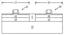
前記基板の上の第1積層スタックで、前記第1積層スタックが前記基板の上に圧縮応力誘電体層と前記圧縮応力誘電体層の上に第1半導体層を有し、前記圧縮応力誘電体層が前記第1半導体層に引張り応力を伝達する、前記第1積層スタックと、
前記基板の上の第2積層スタックで、前記第2積層スタックが前記基板の上に引張り応力誘電体層と前記引張り応力誘電体層の上に第2半導体層を有し、前記引張り応力誘電体層が前記第2半導体層に圧縮応力を伝達する、前記第2積層スタックとを有する。
基板の第1の部分に圧縮応力誘電体層を形成するステップと、
基板の第2の部分に引張り応力誘電体層を形成するステップと、
前記圧縮応力誘電体層と前記引張り応力誘電体層の上に半導体層を形成するステップと、
前記半導体層を貫通し、前記引張り応力誘電体層を前記圧縮応力誘電体層から分離する分離領域を形成するステップで、前記圧縮応力誘電体層が前記圧縮応力誘電体層の上にある前記半導体層の部分に引張り応力を伝達し、前記引張り応力誘電体層が前記引張り応力誘電体層の上にある前記半導体層の部分に圧縮応力を伝達する、前記分離領域を形成するステップとを有する。
基板の第1の部分に引張り応力誘電体層を配置し、前記基板の第2の部分に圧縮応力誘電体層を配置する基板を有する初期構造を提供するステップで、前記引張り応力誘電体層と前記圧縮応力誘電体層を絶縁材料で分離する、前記提供するステップと、
前記Si含有基板の前記第1の部分と前記第2の部分の間の前記基板の部分を露出させるために、前記絶縁材料を除去するステップと、
前記基板の前記第1の部分および前記基板の前記第2の部分に隣接して前記基板に凹部を設けるために、前記基板の前記第1の部分および前記第2の部分から前記基板の前記一部を凹ませるステップと、
前記基板の凹部に配置する酸化物を形成するステップであって、前記酸化物を前記圧縮応力誘電体層および前記引張り応力誘電体層の上面と同じ平面になる厚さに堆積して、平坦な上面にする、前記基板の凹部に配置する酸化物を形成するステップと、
前記酸化物の前記平坦な上面にウェハを接合するステップと、
剥離境界面を設けるために前記基板にイオン注入するステップと、
前記基板の剥離面はそのままの状態で、前記剥離境界面付近で前記基板を分離するステップと、
前記基板の前記凹部上の前記酸化物の表面まで、前記基板の前記剥離面を平坦化するステップで、前記基板の前記酸化物までの平坦化により前記引っ張り誘電体層および前記圧縮誘電体層の上に半導体層を作る、前記平坦化するステップと、
前記酸化物を除去するステップであって、前記引張り応力誘電体層が前記引張り応力誘電体層の上にある前記半導体層に圧縮応力を伝達し、前記圧縮応力誘電体層が前記圧縮応力誘電体層の上にある前記半導体層に引張り応力を伝達する、前記酸化物を除去するステップと、
を有する。
Claims (5)
- 基板を製造する方法であって、
基板の第1の部分に圧縮応力誘電体層を形成するステップと、
基板の第2の部分に引張り応力誘電体層を形成するステップと、
前記圧縮応力誘電体層および前記引張り応力誘電体層の上に半導体層を形成するステップと、
前記半導体層を貫通し、前記引張り応力誘電体層を前記圧縮応力誘電体層から分離する分離領域を形成するステップとを有し、
前記圧縮応力誘電体層が前記圧縮応力誘電体層の上にある前記半導体層の部分に引張り応力を伝達するとともに、前記引張り応力誘電体層が前記引張り応力誘電体層の上にある前記半導体層の部分に圧縮応力を伝達する、
基板を製造する方法。 - 基板を形成する方法であって、
Si含有基板の第1の部分に引張り応力誘電体層を配置し、前記Si含有基板の第2の部分に圧縮応力誘電体層を配置するSi含有基板を有する初期構造を提供するステップであって、前記引張り応力誘電体層と前記圧縮応力誘電体層を絶縁材料で分離する、ステップと、
前記絶縁材料を除去して、前記Si含有基板の前記第1の部分と前記第2の部分の間の前記Si含有基板の部分を露出させるステップと、
前記基板の第1の部分および前記基板の第2の部分に隣接する前記Si含有基板に凹部を設けるように、前記Si含有基板の前記第1の部分および前記第2の部分から前記Si含有基板を凹ませるステップと、
前記Si含有基板の凹部上に配置する酸化物を形成するステップであって、前記酸化物を前記圧縮層および前記引張り層の上面と同一平面上にして平坦な上面を提供する、ステップと、
前記平坦な上面にウェハを接合するステップと、
剥離境界面を提供するように前記Si含有基板にイオン注入するステップと、
前記剥離面の境界付近で前記Si含有基板を分離するステップであって、前記Si含有基板の剥離面はそのままである、ステップと、
前記Si含有基板の前記凹部上の前記酸化物の表面まで、前記Si含有基板の前記剥離面を平坦化するステップであって、前記Si含有基板を前記酸化物に平坦化するステップが前記引張り応力の材料と前記圧縮応力の材料の上に半導体層を作る、ステップと、
前記酸化物を除去するステップであって、前記引張り応力誘電体層が前記半導体層に圧縮応力を伝達し、前記圧縮応力誘電体層が前記半導体層に引張り応力を伝達する、ステップと、を有する方法。 - 前記初期構造を提供するステップが、
前記Si含有基板の上に前記絶縁材料の層を設けるステップと、
前記Si含有基板の前記第1の部分を露出させるように前記絶縁材料の層の第1部分を除去し、前記Si含有基板の前記第2の部分を露出させるように前記絶縁材料の層の第2の部分を除去するステップと、
前記Si含有基板の前記第1の部分の上に前記引張り応力誘電体層を形成し、前記Si含有基板の第2の部分の上に前記圧縮応力誘電体層を形成するステップと、
を有する、請求項2の方法。 - 前記絶縁材料を除去する前に、前記圧縮応力誘電体層および前記引張り応力誘電体層の上にポリシリコン・キャップを形成するステップと、
前記絶縁材料を除去した後で、前記圧縮応力誘電体層および前記引張り応力誘電体層の上の前記ポリシリコン・キャップを除去するステップであって、前記ポリシリコン・キャップが前記圧縮応力誘電体層および引張り応力誘電体層内の応力を維持する、ステップと、
をさらに有する、請求項3の方法。 - 前記基板の第1の部分に圧縮応力誘電体層を形成するステップが、
前記基板上に圧縮応力誘電体層をブランケット堆積するステップと、
前記基板の前記第1の部分の上にある前記圧縮応力誘電体層の部分を保護し、前記圧縮応力誘電体層の残りの部分を露出させたままにする第1の保護マスクを形成するステップと、
前記圧縮応力誘電体層の前記残りの部分を、前記第1の保護マスクと前記基板に対して選択的にエッチングするステップと、
前記第1の保護マスクを除去するステップと、を有する請求項1の方法。
Applications Claiming Priority (3)
| Application Number | Priority Date | Filing Date | Title |
|---|---|---|---|
| US10/905,062 US7262087B2 (en) | 2004-12-14 | 2004-12-14 | Dual stressed SOI substrates |
| US10/905,062 | 2004-12-14 | ||
| PCT/US2005/044957 WO2006065759A2 (en) | 2004-12-14 | 2005-12-13 | Dual stressed soi substrates |
Publications (3)
| Publication Number | Publication Date |
|---|---|
| JP2008523631A JP2008523631A (ja) | 2008-07-03 |
| JP2008523631A5 JP2008523631A5 (ja) | 2008-10-09 |
| JP5039902B2 true JP5039902B2 (ja) | 2012-10-03 |
Family
ID=36582810
Family Applications (1)
| Application Number | Title | Priority Date | Filing Date |
|---|---|---|---|
| JP2007545712A Expired - Fee Related JP5039902B2 (ja) | 2004-12-14 | 2005-12-13 | デュアル・ストレス(二重応力)soi基板の製造方法および半導体デバイス |
Country Status (8)
| Country | Link |
|---|---|
| US (2) | US7262087B2 (ja) |
| EP (1) | EP1825509B1 (ja) |
| JP (1) | JP5039902B2 (ja) |
| CN (1) | CN100495687C (ja) |
| AT (1) | ATE487234T1 (ja) |
| DE (1) | DE602005024611D1 (ja) |
| TW (1) | TWI366264B (ja) |
| WO (1) | WO2006065759A2 (ja) |
Families Citing this family (39)
| Publication number | Priority date | Publication date | Assignee | Title |
|---|---|---|---|---|
| JP4157496B2 (ja) | 2004-06-08 | 2008-10-01 | 株式会社東芝 | 半導体装置及びその製造方法 |
| US7202513B1 (en) * | 2005-09-29 | 2007-04-10 | International Business Machines Corporation | Stress engineering using dual pad nitride with selective SOI device architecture |
| US8319285B2 (en) * | 2005-12-22 | 2012-11-27 | Infineon Technologies Ag | Silicon-on-insulator chip having multiple crystal orientations |
| JP2007335573A (ja) * | 2006-06-14 | 2007-12-27 | Hitachi Ltd | 半導体装置およびその製造方法 |
| US7803690B2 (en) * | 2006-06-23 | 2010-09-28 | Taiwan Semiconductor Manufacturing Company, Ltd. | Epitaxy silicon on insulator (ESOI) |
| JP5532527B2 (ja) * | 2006-08-03 | 2014-06-25 | 株式会社デンソー | Soi基板およびその製造方法 |
| US7829407B2 (en) * | 2006-11-20 | 2010-11-09 | International Business Machines Corporation | Method of fabricating a stressed MOSFET by bending SOI region |
| US7888197B2 (en) * | 2007-01-11 | 2011-02-15 | International Business Machines Corporation | Method of forming stressed SOI FET having doped glass box layer using sacrificial stressed layer |
| US20080185655A1 (en) * | 2007-02-02 | 2008-08-07 | United Microelectronics Corp. | Smiconductor device, method for fabricating thereof and method for increasing film stress |
| US20080203485A1 (en) * | 2007-02-28 | 2008-08-28 | International Business Machines Corporation | Strained metal gate structure for cmos devices with improved channel mobility and methods of forming the same |
| US20080237733A1 (en) * | 2007-03-27 | 2008-10-02 | International Business Machines Corporation | Structure and method to enhance channel stress by using optimized sti stress and nitride capping layer stress |
| US7615435B2 (en) * | 2007-07-31 | 2009-11-10 | International Business Machines Corporation | Semiconductor device and method of manufacture |
| US20090095991A1 (en) * | 2007-10-11 | 2009-04-16 | International Business Machines Corporation | Method of forming strained mosfet devices using phase transformable materials |
| US20090140351A1 (en) * | 2007-11-30 | 2009-06-04 | Hong-Nien Lin | MOS Devices Having Elevated Source/Drain Regions |
| US7883956B2 (en) * | 2008-02-15 | 2011-02-08 | International Business Machines Corporation | Method of forming coplanar active and isolation regions and structures thereof |
| US8232186B2 (en) * | 2008-05-29 | 2012-07-31 | International Business Machines Corporation | Methods of integrating reverse eSiGe on NFET and SiGe channel on PFET, and related structure |
| EP2300953B1 (en) * | 2008-06-13 | 2013-01-23 | Nxp B.V. | Intrusion protection using stress changes |
| FR2934085B1 (fr) * | 2008-07-21 | 2010-09-03 | Commissariat Energie Atomique | Procede pour containdre simultanement en tension et en compression les canaux de transistors nmos et pmos respectivement |
| US8138523B2 (en) * | 2009-10-08 | 2012-03-20 | International Business Machines Corporation | Semiconductor device having silicon on stressed liner (SOL) |
| CN102549729B (zh) * | 2009-12-16 | 2015-01-07 | 国家半导体公司 | 用于半导体衬底上的大面积的基于氮化镓或其它氮化物的结构的应力补偿 |
| WO2011096265A1 (ja) * | 2010-02-04 | 2011-08-11 | シャープ株式会社 | 転写方法および半導体装置の製造方法並びに半導体装置 |
| US8216905B2 (en) * | 2010-04-27 | 2012-07-10 | Taiwan Semiconductor Manufacturing Company, Ltd. | Stress engineering to reduce dark current of CMOS image sensors |
| US8318563B2 (en) | 2010-05-19 | 2012-11-27 | National Semiconductor Corporation | Growth of group III nitride-based structures and integration with conventional CMOS processing tools |
| US8377759B2 (en) | 2010-08-17 | 2013-02-19 | International Business Machines Corporation | Controlled fin-merging for fin type FET devices |
| US8592292B2 (en) | 2010-09-02 | 2013-11-26 | National Semiconductor Corporation | Growth of multi-layer group III-nitride buffers on large-area silicon substrates and other substrates |
| US9064974B2 (en) * | 2011-05-16 | 2015-06-23 | International Business Machines Corporation | Barrier trench structure and methods of manufacture |
| US8921209B2 (en) | 2012-09-12 | 2014-12-30 | International Business Machines Corporation | Defect free strained silicon on insulator (SSOI) substrates |
| CN103296013B (zh) * | 2013-05-28 | 2017-08-08 | 上海华虹宏力半导体制造有限公司 | 射频器件的形成方法 |
| US9018057B1 (en) | 2013-10-08 | 2015-04-28 | Stmicroelectronics, Inc. | Method of making a CMOS semiconductor device using a stressed silicon-on-insulator (SOI) wafer |
| US9190467B2 (en) | 2014-01-08 | 2015-11-17 | Macronix International Co., Ltd. | Semiconductor structure and manufacturing method of the same |
| US20150371905A1 (en) * | 2014-06-20 | 2015-12-24 | Rf Micro Devices, Inc. | Soi with gold-doped handle wafer |
| US20150372096A1 (en) * | 2014-06-20 | 2015-12-24 | Ishiang Shih | High Electron Mobility Transistors and Integrated Circuits with Improved Feature Uniformity and Reduced defects for Microwave and Millimetre Wave Applications |
| US9716581B2 (en) * | 2014-07-31 | 2017-07-25 | Akoustis, Inc. | Mobile communication device configured with a single crystal piezo resonator structure |
| US9515181B2 (en) | 2014-08-06 | 2016-12-06 | Qualcomm Incorporated | Semiconductor device with self-aligned back side features |
| US9570360B2 (en) | 2014-08-27 | 2017-02-14 | International Business Machines Corporation | Dual channel material for finFET for high performance CMOS |
| US9543323B2 (en) | 2015-01-13 | 2017-01-10 | International Business Machines Corporation | Strain release in PFET regions |
| JP2018101740A (ja) * | 2016-12-21 | 2018-06-28 | ソニーセミコンダクタソリューションズ株式会社 | 半導体装置、半導体装置の製造方法、及び、電子機器 |
| TWI622169B (zh) * | 2017-02-17 | 2018-04-21 | Powerchip Technology Corporation | 半導體元件的製造方法 |
| CN110660773A (zh) * | 2018-06-28 | 2020-01-07 | 晟碟信息科技(上海)有限公司 | 包含应力消除层的半导体产品衬底 |
Family Cites Families (83)
| Publication number | Priority date | Publication date | Assignee | Title |
|---|---|---|---|---|
| US3602841A (en) | 1970-06-18 | 1971-08-31 | Ibm | High frequency bulk semiconductor amplifiers and oscillators |
| GB1601059A (en) * | 1978-05-31 | 1981-10-21 | Secr Defence | Fet devices and their fabrication |
| US4853076A (en) | 1983-12-29 | 1989-08-01 | Massachusetts Institute Of Technology | Semiconductor thin films |
| US4655415A (en) | 1985-01-24 | 1987-04-07 | The Garrett Corporation | Helicopter flotation |
| US4665415A (en) | 1985-04-24 | 1987-05-12 | International Business Machines Corporation | Semiconductor device with hole conduction via strained lattice |
| DE3676781D1 (de) | 1985-09-13 | 1991-02-14 | Siemens Ag | Integrierte bipolar- und komplementaere mos-transistoren auf einem gemeinsamen substrat enthaltende schaltung und verfahren zu ihrer herstellung. |
| US4958213A (en) | 1987-12-07 | 1990-09-18 | Texas Instruments Incorporated | Method for forming a transistor base region under thick oxide |
| US5354695A (en) | 1992-04-08 | 1994-10-11 | Leedy Glenn J | Membrane dielectric isolation IC fabrication |
| US5459346A (en) | 1988-06-28 | 1995-10-17 | Ricoh Co., Ltd. | Semiconductor substrate with electrical contact in groove |
| US5006913A (en) | 1988-11-05 | 1991-04-09 | Mitsubishi Denki Kabushiki Kaisha | Stacked type semiconductor device |
| US5108843A (en) | 1988-11-30 | 1992-04-28 | Ricoh Company, Ltd. | Thin film semiconductor and process for producing the same |
| US4952524A (en) | 1989-05-05 | 1990-08-28 | At&T Bell Laboratories | Semiconductor device manufacture including trench formation |
| US5013681A (en) * | 1989-09-29 | 1991-05-07 | The United States Of America As Represented By The Secretary Of The Navy | Method of producing a thin silicon-on-insulator layer |
| US5310446A (en) | 1990-01-10 | 1994-05-10 | Ricoh Company, Ltd. | Method for producing semiconductor film |
| US5060030A (en) | 1990-07-18 | 1991-10-22 | Raytheon Company | Pseudomorphic HEMT having strained compensation layer |
| US5218213A (en) * | 1991-02-22 | 1993-06-08 | Harris Corporation | SOI wafer with sige |
| US5081513A (en) | 1991-02-28 | 1992-01-14 | Xerox Corporation | Electronic device with recovery layer proximate to active layer |
| US5371399A (en) | 1991-06-14 | 1994-12-06 | International Business Machines Corporation | Compound semiconductor having metallic inclusions and devices fabricated therefrom |
| US5134085A (en) | 1991-11-21 | 1992-07-28 | Micron Technology, Inc. | Reduced-mask, split-polysilicon CMOS process, incorporating stacked-capacitor cells, for fabricating multi-megabit dynamic random access memories |
| US5391510A (en) | 1992-02-28 | 1995-02-21 | International Business Machines Corporation | Formation of self-aligned metal gate FETs using a benignant removable gate material during high temperature steps |
| US6008126A (en) | 1992-04-08 | 1999-12-28 | Elm Technology Corporation | Membrane dielectric isolation IC fabrication |
| US5268326A (en) * | 1992-09-28 | 1993-12-07 | Motorola, Inc. | Method of making dielectric and conductive isolated island |
| US5234535A (en) * | 1992-12-10 | 1993-08-10 | International Business Machines Corporation | Method of producing a thin silicon-on-insulator layer |
| US5561302A (en) | 1994-09-26 | 1996-10-01 | Motorola, Inc. | Enhanced mobility MOSFET device and method |
| US5405791A (en) * | 1994-10-04 | 1995-04-11 | Micron Semiconductor, Inc. | Process for fabricating ULSI CMOS circuits using a single polysilicon gate layer and disposable spacers |
| US5444014A (en) * | 1994-12-16 | 1995-08-22 | Electronics And Telecommunications Research Institute | Method for fabricating semiconductor device |
| US5670387A (en) * | 1995-01-03 | 1997-09-23 | Motorola, Inc. | Process for forming semiconductor-on-insulator device |
| US5670798A (en) | 1995-03-29 | 1997-09-23 | North Carolina State University | Integrated heterostructures of Group III-V nitride semiconductor materials including epitaxial ohmic contact non-nitride buffer layer and methods of fabricating same |
| US5679965A (en) | 1995-03-29 | 1997-10-21 | North Carolina State University | Integrated heterostructures of Group III-V nitride semiconductor materials including epitaxial ohmic contact, non-nitride buffer layer and methods of fabricating same |
| US5557122A (en) | 1995-05-12 | 1996-09-17 | Alliance Semiconductors Corporation | Semiconductor electrode having improved grain structure and oxide growth properties |
| US6403975B1 (en) | 1996-04-09 | 2002-06-11 | Max-Planck Gesellschaft Zur Forderung Der Wissenschafteneev | Semiconductor components, in particular photodetectors, light emitting diodes, optical modulators and waveguides with multilayer structures grown on silicon substrates |
| US5880040A (en) | 1996-04-15 | 1999-03-09 | Macronix International Co., Ltd. | Gate dielectric based on oxynitride grown in N2 O and annealed in NO |
| US5861651A (en) | 1997-02-28 | 1999-01-19 | Lucent Technologies Inc. | Field effect devices and capacitors with improved thin film dielectrics and method for making same |
| US5940736A (en) | 1997-03-11 | 1999-08-17 | Lucent Technologies Inc. | Method for forming a high quality ultrathin gate oxide layer |
| US6309975B1 (en) | 1997-03-14 | 2001-10-30 | Micron Technology, Inc. | Methods of making implanted structures |
| US6025280A (en) | 1997-04-28 | 2000-02-15 | Lucent Technologies Inc. | Use of SiD4 for deposition of ultra thin and controllable oxides |
| US5960297A (en) | 1997-07-02 | 1999-09-28 | Kabushiki Kaisha Toshiba | Shallow trench isolation structure and method of forming the same |
| JP3139426B2 (ja) | 1997-10-15 | 2001-02-26 | 日本電気株式会社 | 半導体装置 |
| US6066545A (en) | 1997-12-09 | 2000-05-23 | Texas Instruments Incorporated | Birdsbeak encroachment using combination of wet and dry etch for isolation nitride |
| US6274421B1 (en) | 1998-01-09 | 2001-08-14 | Sharp Laboratories Of America, Inc. | Method of making metal gate sub-micron MOS transistor |
| KR100275908B1 (ko) | 1998-03-02 | 2000-12-15 | 윤종용 | 집적 회로에 트렌치 아이솔레이션을 형성하는방법 |
| US6361885B1 (en) | 1998-04-10 | 2002-03-26 | Organic Display Technology | Organic electroluminescent materials and device made from such materials |
| US6165383A (en) | 1998-04-10 | 2000-12-26 | Organic Display Technology | Useful precursors for organic electroluminescent materials and devices made from such materials |
| US5989978A (en) | 1998-07-16 | 1999-11-23 | Chartered Semiconductor Manufacturing, Ltd. | Shallow trench isolation of MOSFETS with reduced corner parasitic currents |
| JP4592837B2 (ja) | 1998-07-31 | 2010-12-08 | ルネサスエレクトロニクス株式会社 | 半導体装置の製造方法 |
| US6319794B1 (en) | 1998-10-14 | 2001-11-20 | International Business Machines Corporation | Structure and method for producing low leakage isolation devices |
| US6235598B1 (en) | 1998-11-13 | 2001-05-22 | Intel Corporation | Method of using thick first spacers to improve salicide resistance on polysilicon gates |
| US6117722A (en) | 1999-02-18 | 2000-09-12 | Taiwan Semiconductor Manufacturing Company | SRAM layout for relaxing mechanical stress in shallow trench isolation technology and method of manufacture thereof |
| US6255169B1 (en) | 1999-02-22 | 2001-07-03 | Advanced Micro Devices, Inc. | Process for fabricating a high-endurance non-volatile memory device |
| US6284626B1 (en) | 1999-04-06 | 2001-09-04 | Vantis Corporation | Angled nitrogen ion implantation for minimizing mechanical stress on side walls of an isolation trench |
| US6656822B2 (en) | 1999-06-28 | 2003-12-02 | Intel Corporation | Method for reduced capacitance interconnect system using gaseous implants into the ILD |
| US6228694B1 (en) | 1999-06-28 | 2001-05-08 | Intel Corporation | Method of increasing the mobility of MOS transistors by use of localized stress regions |
| US6362082B1 (en) | 1999-06-28 | 2002-03-26 | Intel Corporation | Methodology for control of short channel effects in MOS transistors |
| US6281532B1 (en) | 1999-06-28 | 2001-08-28 | Intel Corporation | Technique to obtain increased channel mobilities in NMOS transistors by gate electrode engineering |
| KR100332108B1 (ko) | 1999-06-29 | 2002-04-10 | 박종섭 | 반도체 소자의 트랜지스터 및 그 제조 방법 |
| TW426940B (en) | 1999-07-30 | 2001-03-21 | United Microelectronics Corp | Manufacturing method of MOS field effect transistor |
| JP3275896B2 (ja) * | 1999-10-06 | 2002-04-22 | 日本電気株式会社 | 半導体装置の製造方法 |
| US6284623B1 (en) | 1999-10-25 | 2001-09-04 | Peng-Fei Zhang | Method of fabricating semiconductor devices using shallow trench isolation with reduced narrow channel effect |
| US6476462B2 (en) | 1999-12-28 | 2002-11-05 | Texas Instruments Incorporated | MOS-type semiconductor device and method for making same |
| US6221735B1 (en) | 2000-02-15 | 2001-04-24 | Philips Semiconductors, Inc. | Method for eliminating stress induced dislocations in CMOS devices |
| US6531369B1 (en) | 2000-03-01 | 2003-03-11 | Applied Micro Circuits Corporation | Heterojunction bipolar transistor (HBT) fabrication using a selectively deposited silicon germanium (SiGe) |
| JP4963140B2 (ja) * | 2000-03-02 | 2012-06-27 | 株式会社半導体エネルギー研究所 | 半導体装置 |
| US6368931B1 (en) | 2000-03-27 | 2002-04-09 | Intel Corporation | Thin tensile layers in shallow trench isolation and method of making same |
| US6380021B1 (en) * | 2000-06-20 | 2002-04-30 | Taiwan Semiconductor Manufacturing Company | Ultra-shallow junction formation by novel process sequence for PMOSFET |
| US6493497B1 (en) | 2000-09-26 | 2002-12-10 | Motorola, Inc. | Electro-optic structure and process for fabricating same |
| US6501121B1 (en) | 2000-11-15 | 2002-12-31 | Motorola, Inc. | Semiconductor structure |
| AU2001267880A1 (en) * | 2000-11-22 | 2002-06-03 | Hitachi Ltd. | Semiconductor device and method for fabricating the same |
| JP2003086708A (ja) * | 2000-12-08 | 2003-03-20 | Hitachi Ltd | 半導体装置及びその製造方法 |
| US6563152B2 (en) * | 2000-12-29 | 2003-05-13 | Intel Corporation | Technique to obtain high mobility channels in MOS transistors by forming a strain layer on an underside of a channel |
| US20020086497A1 (en) | 2000-12-30 | 2002-07-04 | Kwok Siang Ping | Beaker shape trench with nitride pull-back for STI |
| US6265317B1 (en) | 2001-01-09 | 2001-07-24 | Taiwan Semiconductor Manufacturing Company | Top corner rounding for shallow trench isolation |
| US6403486B1 (en) | 2001-04-30 | 2002-06-11 | Taiwan Semiconductor Manufacturing Company | Method for forming a shallow trench isolation |
| US6531740B2 (en) | 2001-07-17 | 2003-03-11 | Motorola, Inc. | Integrated impedance matching and stability network |
| US6498358B1 (en) | 2001-07-20 | 2002-12-24 | Motorola, Inc. | Structure and method for fabricating an electro-optic system having an electrochromic diffraction grating |
| US6908810B2 (en) | 2001-08-08 | 2005-06-21 | Taiwan Semiconductor Manufacturing Co., Ltd. | Method of preventing threshold voltage of MOS transistor from being decreased by shallow trench isolation formation |
| JP2003060076A (ja) | 2001-08-21 | 2003-02-28 | Nec Corp | 半導体装置及びその製造方法 |
| US20030057184A1 (en) | 2001-09-22 | 2003-03-27 | Shiuh-Sheng Yu | Method for pull back SiN to increase rounding effect in a shallow trench isolation process |
| US6656798B2 (en) | 2001-09-28 | 2003-12-02 | Infineon Technologies, Ag | Gate processing method with reduced gate oxide corner and edge thinning |
| US6717216B1 (en) * | 2002-12-12 | 2004-04-06 | International Business Machines Corporation | SOI based field effect transistor having a compressive film in undercut area under the channel and a method of making the device |
| US6878611B2 (en) * | 2003-01-02 | 2005-04-12 | International Business Machines Corporation | Patterned strained silicon for high performance circuits |
| US6911379B2 (en) * | 2003-03-05 | 2005-06-28 | Taiwan Semiconductor Manufacturing Company, Ltd. | Method of forming strained silicon on insulator substrate |
| US7812340B2 (en) * | 2003-06-13 | 2010-10-12 | International Business Machines Corporation | Strained-silicon-on-insulator single-and double-gate MOSFET and method for forming the same |
| US7125759B2 (en) * | 2005-03-23 | 2006-10-24 | Taiwan Semiconductor Manufacturing Co., Ltd. | Semiconductor-on-insulator (SOI) strained active areas |
-
2004
- 2004-12-14 US US10/905,062 patent/US7262087B2/en active Active
-
2005
- 2005-12-02 TW TW094142702A patent/TWI366264B/zh active
- 2005-12-13 AT AT05853786T patent/ATE487234T1/de not_active IP Right Cessation
- 2005-12-13 WO PCT/US2005/044957 patent/WO2006065759A2/en active Application Filing
- 2005-12-13 JP JP2007545712A patent/JP5039902B2/ja not_active Expired - Fee Related
- 2005-12-13 DE DE602005024611T patent/DE602005024611D1/de active Active
- 2005-12-13 CN CN200580042739.8A patent/CN100495687C/zh not_active Expired - Fee Related
- 2005-12-13 EP EP05853786A patent/EP1825509B1/en not_active Not-in-force
-
2007
- 2007-04-27 US US11/741,441 patent/US7312134B2/en not_active Expired - Fee Related
Also Published As
| Publication number | Publication date |
|---|---|
| WO2006065759A3 (en) | 2007-06-14 |
| DE602005024611D1 (de) | 2010-12-16 |
| CN101076889A (zh) | 2007-11-21 |
| US20070202639A1 (en) | 2007-08-30 |
| EP1825509A2 (en) | 2007-08-29 |
| US20060125008A1 (en) | 2006-06-15 |
| EP1825509B1 (en) | 2010-11-03 |
| TW200636979A (en) | 2006-10-16 |
| JP2008523631A (ja) | 2008-07-03 |
| ATE487234T1 (de) | 2010-11-15 |
| US7312134B2 (en) | 2007-12-25 |
| TWI366264B (en) | 2012-06-11 |
| EP1825509A4 (en) | 2009-04-15 |
| CN100495687C (zh) | 2009-06-03 |
| US7262087B2 (en) | 2007-08-28 |
| WO2006065759A2 (en) | 2006-06-22 |
Similar Documents
| Publication | Publication Date | Title |
|---|---|---|
| JP5039902B2 (ja) | デュアル・ストレス(二重応力)soi基板の製造方法および半導体デバイス | |
| JP4814304B2 (ja) | 集積回路およびその製造方法 | |
| US7605429B2 (en) | Hybrid crystal orientation CMOS structure for adaptive well biasing and for power and performance enhancement | |
| US7560328B2 (en) | Strained Si on multiple materials for bulk or SOI substrates | |
| US9040373B2 (en) | Silicon device on SI:C-OI and SGOI and method of manufacture | |
| US7619300B2 (en) | Super hybrid SOI CMOS devices | |
| US7034362B2 (en) | Double silicon-on-insulator (SOI) metal oxide semiconductor field effect transistor (MOSFET) structures | |
| US7498216B2 (en) | Method of forming high-performance CMOS SOI devices on hybrid crystal-oriented substrates | |
| US7528056B2 (en) | Low-cost strained SOI substrate for high-performance CMOS technology | |
| TW200525765A (en) | Strained dislocation-free channels for CMOS and method of manufacture | |
| US20130285118A1 (en) | CMOS WITH SiGe CHANNEL PFETs AND METHOD OF FABRICATION | |
| EP2050128A2 (en) | Raised sti structure and superdamascene technique for nmosfet performance enhancement with embedded silicon carbon | |
| JP4328708B2 (ja) | Cmosデバイスの製造方法及びcmosデバイスを備える構造 | |
| JP2006012995A (ja) | 半導体装置及びその製造方法 |
Legal Events
| Date | Code | Title | Description |
|---|---|---|---|
| A521 | Request for written amendment filed |
Free format text: JAPANESE INTERMEDIATE CODE: A523 Effective date: 20080822 |
|
| A621 | Written request for application examination |
Free format text: JAPANESE INTERMEDIATE CODE: A621 Effective date: 20080822 |
|
| A977 | Report on retrieval |
Free format text: JAPANESE INTERMEDIATE CODE: A971007 Effective date: 20111128 |
|
| A131 | Notification of reasons for refusal |
Free format text: JAPANESE INTERMEDIATE CODE: A131 Effective date: 20111206 |
|
| A521 | Request for written amendment filed |
Free format text: JAPANESE INTERMEDIATE CODE: A523 Effective date: 20120130 |
|
| RD12 | Notification of acceptance of power of sub attorney |
Free format text: JAPANESE INTERMEDIATE CODE: A7432 Effective date: 20120130 |
|
| A521 | Request for written amendment filed |
Free format text: JAPANESE INTERMEDIATE CODE: A821 Effective date: 20120130 |
|
| A131 | Notification of reasons for refusal |
Free format text: JAPANESE INTERMEDIATE CODE: A131 Effective date: 20120313 |
|
| A521 | Request for written amendment filed |
Free format text: JAPANESE INTERMEDIATE CODE: A523 Effective date: 20120318 |
|
| A01 | Written decision to grant a patent or to grant a registration (utility model) |
Free format text: JAPANESE INTERMEDIATE CODE: A01 Effective date: 20120417 |
|
| RD14 | Notification of resignation of power of sub attorney |
Free format text: JAPANESE INTERMEDIATE CODE: A7434 Effective date: 20120417 |
|
| A01 | Written decision to grant a patent or to grant a registration (utility model) |
Free format text: JAPANESE INTERMEDIATE CODE: A01 |
|
| A61 | First payment of annual fees (during grant procedure) |
Free format text: JAPANESE INTERMEDIATE CODE: A61 Effective date: 20120511 |
|
| R150 | Certificate of patent or registration of utility model |
Free format text: JAPANESE INTERMEDIATE CODE: R150 |
|
| FPAY | Renewal fee payment (event date is renewal date of database) |
Free format text: PAYMENT UNTIL: 20150720 Year of fee payment: 3 |
|
| R250 | Receipt of annual fees |
Free format text: JAPANESE INTERMEDIATE CODE: R250 |
|
| R250 | Receipt of annual fees |
Free format text: JAPANESE INTERMEDIATE CODE: R250 |
|
| LAPS | Cancellation because of no payment of annual fees |