JP5016807B2 - Data processing system - Google Patents
Data processing system Download PDFInfo
- Publication number
- JP5016807B2 JP5016807B2 JP2005294288A JP2005294288A JP5016807B2 JP 5016807 B2 JP5016807 B2 JP 5016807B2 JP 2005294288 A JP2005294288 A JP 2005294288A JP 2005294288 A JP2005294288 A JP 2005294288A JP 5016807 B2 JP5016807 B2 JP 5016807B2
- Authority
- JP
- Japan
- Prior art keywords
- data processing
- software
- hardware
- module
- programmable logic
- Prior art date
- Legal status (The legal status is an assumption and is not a legal conclusion. Google has not performed a legal analysis and makes no representation as to the accuracy of the status listed.)
- Expired - Fee Related
Links
Images


Description
本発明は、プログラマブル論理回路を用途に合わせて変更するデータ処理システムに関するものである。 The present invention relates to a data processing system that changes a programmable logic circuit in accordance with a use.
半導体の微細化の進展により、プロセッサの能力は増大し、従来ハードウェアで行っていた処理もソフトウェアで行うことが可能となってきた。このプロセッサの性能を生かして、多くの処理のソフトウェア化が進められている。特定アプリケーションごとにソフトウェアを作成するのではなく、基本単位ごとにライブラリ化を行い、各アプリケーションに対しては、ライブラリの組み合わせとして機能を実現してきた。例えば、画像処理分野では、各アプリケーションで異なる処理が必要となるため、ソフトウェアのライブラリ化を推し進め、ライブラリの組み合わせで必要なデータを生成するやり方が主流となってきている。 With the progress of miniaturization of semiconductors, the capability of processors has increased, and it has become possible to perform processing that has been conventionally performed by hardware using software. Utilizing the performance of this processor, many processes are being made into software. Rather than creating software for each specific application, a library is created for each basic unit, and functions have been realized as combinations of libraries for each application. For example, in the image processing field, different processes are required for each application, and therefore, a method of promoting software library formation and generating necessary data by combining libraries has become mainstream.
しかし、汎用的に作られるプロセッサはコストとの関係で最小公倍数的な機能しかサポートできず、その他、大部分の処理に関しては未だに複数の処理を組み合わせて実行するレベルに留まっている。例えば、マルチメディア関連の命令でSIMD(Single
Instruction/Multiple Data)処理も、積和演算のレベルに留まっているため、これを複数実行する画像処理やデータ処理に関してはソフトウェアでSIMDを複数回実行する形態を取っている。MPEG2デコードやMP3でコードなどは、この処理でリアルタイム性を確保できるが、画像のエッジ処理や特定周波数の抽出などのアプリケーションに特化した機能は、複数の処理となるためリアルタイム性を確保できない。
However, a general-purpose processor can support only the least common multiple function in relation to cost, and most other processes are still at a level where a plurality of processes are combined and executed. For example, a multimedia-related command is SIMD (Single
Since Instruction / Multiple Data) processing also remains at the level of product-sum operation, image processing and data processing for executing a plurality of these operations take a form in which SIMD is executed a plurality of times by software. For MPEG2 decoding and MP3 codes, real-time performance can be ensured by this processing, but functions specialized for applications such as image edge processing and specific frequency extraction cannot be secured because they are a plurality of processes.
そのため特定処理の高速化は、専用のハードウェアを用いて処理時間を短縮して高速化を実現してきた。このハードウェアはG/AやCBICをアプリケーションに合わせて作成していたが、今度は逆に、半導体の微細化が開発費を押し上げ、数百万個/月以上の使用量がなければ、開発費を回収できない事態となってきている。そこで、回路規模や動作周波数もG/AやCBICに近づいてきたプログラマブル論理回路がその代替として広く使用されるようになってきた。特許文献1には、ソフトウェアとハードウェアの処理時間,メモリー消費量,FPGAの再構成時間を考慮して、実行モジュールを決定する技術が開示されている。 Therefore, the speeding up of the specific processing has been realized by shortening the processing time by using dedicated hardware. For this hardware, G / A and CBIC were created according to the application, but on the contrary, the miniaturization of the semiconductor increased the development cost, and if there was no usage of millions of units / month or more, it was developed. It has become a situation where expenses cannot be recovered. Therefore, programmable logic circuits whose circuit scale and operating frequency have approached G / A and CBIC have come to be widely used as alternatives. Patent Document 1 discloses a technique for determining an execution module in consideration of software and hardware processing time, memory consumption, and FPGA reconfiguration time.
必要なデータ処理の多くは、複数のアルゴリズムの順番で決定されることが多い。例えば、産業システムでの遠隔操作では、遠隔操作側での画像を取得する必要があるため画像圧縮を行うが、この画像圧縮では離散コサイン変換(DCT)の後、符号化を行う手順を踏むため、DCTのアルゴリズムと符号化のアルゴリズムの組み合わせとなる。このようなアルゴリズムの組み合わせで行われる処理(処理手順)は、ユーザーにより様々であるため、プログラマブル論理回路とはいえソフトウェアほど柔軟に対応できるものではなく、本来ユーザー毎にプログラマブル論理回路を作成すべきであるが、そこまでの対応は出来ないため、プロセッサと同じく最小公倍数的な機能しかサポートしないプログラマブル論理回路を作成している。 Many of the necessary data processing is often determined in the order of a plurality of algorithms. For example, in remote operation in an industrial system, image compression is performed because it is necessary to acquire an image on the remote operation side. However, in this image compression, the procedure for encoding is performed after discrete cosine transform (DCT). , A combination of a DCT algorithm and an encoding algorithm. Since the processing (processing procedure) performed by such a combination of algorithms varies depending on the user, the programmable logic circuit is not as flexible as software, but a programmable logic circuit should be created for each user. However, since it is not possible to cope with it, a programmable logic circuit that supports only the function of the least common multiple like the processor is created.
また、装置に内蔵されているデータ処理部分は、対象となるものが変わると、データ処理自体も変わることがあり、プログラマブル論理回路自体を再設計する必要もある。 In addition, the data processing part built in the apparatus may change if the target is changed, and the programmable logic circuit itself needs to be redesigned.
本発明の目的は、プログラマブル論理回路を搭載しているデータ処理装置において、データ処理に応じて自由にプログラマブル論理回路を変更し、尚且つそのためのソフトウェアも提供するためのシステムを実現するためのものである。 An object of the present invention is to realize a system for freely changing a programmable logic circuit according to data processing and providing software for the same in a data processing apparatus equipped with a programmable logic circuit. It is.
本発明では、入力されたデータの処理手順を含む情報から、ソフトウェアモジュールとハードウェアモジュールを生成し、この各モジュールを実行するデータ処理システムを提案する。 The present invention proposes a data processing system that generates a software module and a hardware module from information including a processing procedure of input data and executes each module.
本発明の効果の一例として、以下のようなものが挙げられる。 Examples of the effects of the present invention include the following.
まず、ユーザー側でデータ処理装置の処理内容の変更が発生した場合、端末を用いてホスト側に新しい処理内容を入力することにより、ユーザーが持っているプログラマブル論理回路の規模に応じてハードウェアモジュールとソフトウェアモジュールを生成し、ダウンロードすることが可能である。このシステムを使用することにより、新しい処理内容に対して最適なデータ処理を行うことが実現できる。 First, when the processing content of the data processing device changes on the user side, the hardware module is input according to the scale of the programmable logic circuit that the user has by inputting new processing content on the host side using a terminal. It is possible to generate and download software modules. By using this system, it is possible to realize optimum data processing for new processing contents.
次に本発明の一例である制御システムは、データ処理装置が端末の機能を持つことにより、データ処理装置のみでホストに対して入力が実現できる。 Next, in the control system as an example of the present invention, the data processing apparatus has the function of a terminal, so that the input to the host can be realized only by the data processing apparatus.
次に本発明の他の一例である制御システムは、ユーザー側にソフトウェアモジュールとハードウェアモジュールの生成機能を持ち、ソフトウェアライブラリとハードウェアライブラリをネットワークに接続されたサーバに持つことにより、例えばホストをユーザー側に持つことにより、さらにソフトウェアモジュールとハードウェアモジュールの最適化を高めることが実現できる。 Next, a control system as another example of the present invention has a function of generating software modules and hardware modules on the user side, and has a software library and a hardware library in a server connected to a network, for example, a host. By having it on the user side, further optimization of software modules and hardware modules can be realized.
本発明の更に他の一例である制御システムは、データ処理装置がホストの機能を持つことにより、データ処理装置と連動してソフトウェアモジュールとハードウェアモジュールの生成が実現できる。 The control system which is still another example of the present invention can realize generation of a software module and a hardware module in conjunction with the data processing device by the data processing device having a host function.
本発明の更に他の一例である制御システムは、ソフトウェアモジュールとハードウェアモジュール生成時に制約条件を満たす最適な組み合わせを実現することができる。 The control system, which is still another example of the present invention, can realize an optimal combination that satisfies the constraint conditions when generating the software module and the hardware module.
プログラマブル論理回路を実装したデータ処理端末において、処理内容が変更した場合のユーザーによるプログラマブル論理回路の変更という目的を、ハードウェアライブラリ及びソフトウェアライブラリと、ユーザーが入力するデータ処理手順・処理時間制約・データ処理装置が持つプログラマブル論理回路の規模の情報から、簡便に実現する In a data processing terminal equipped with a programmable logic circuit, the hardware library and software library and the data processing procedure, processing time constraints, and data input by the user for the purpose of changing the programmable logic circuit by the user when the processing contents are changed Easily realized from the information of the scale of the programmable logic circuit that the processor has
以下、図面を用いて、本発明の第1の実施例について説明する。 Hereinafter, a first embodiment of the present invention will be described with reference to the drawings.
図1に示すように、データ処理装置101,端末102,ホスト103と、それらを接続するネットワーク104から構成される。
As shown in FIG. 1, a
データ処理装置は、図2に示す通り、プロセッサ201,通信インターフェス202,プログラマブル論理回路203,記憶装置204から構成される。
As shown in FIG. 2, the data processing apparatus includes a
次に、一連の処理の流れを図3をもとに説明する。ユーザーが端末103を用いて、データ処理手順と、処理時間制約と、データ処理装置が持つプログラマブル論理回路の規模を入力すると、そのデータがホストに転送される(301)。ホスト側では図4に示す処理に従って、図5に示すソフトウェアライブラリ501とハードウェアライブラリ502をもとに、ソフトウェアモジュール/ハードウェアモジュール303を生成する。ソフトウェアライブラリ501には処理時間データ503と処理に対応するソフトウェア504が、ハードウェアライブラリ502内には処理時間データ505と処理に対応する処理ドライバ506と処理ハードウェア507が入っている。この処理時間データ503と処理時間データ505の情報をもとに、入力された前記処理時間制約と前記プログラマブル論理回路規模に、必要であればデータ量(画像の大きさ)も情報として入力し、これからハードウェアモジュール/ソフトウェアモジュール303を生成する。
Next, a flow of a series of processes will be described with reference to FIG. When the user inputs a data processing procedure, processing time constraints, and the scale of a programmable logic circuit included in the data processing apparatus using the
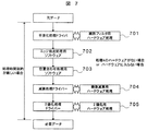
この手順を欠陥抽出の手順を示している図6をもとに説明する。欠陥抽出は、産業用途向けの検査装置などに利用される一般的な手法である。この場合、ノイズ除去機能601,2画像位置合わせ機能602,比較機能603,特徴点抽出機能604を入力する。その後、ノイズ除去機能601は平滑化処理605とエッジ抽出処理606に、2画像位置合わせ機能602は位置合わせ処理607に、比較機能63は減算処理608に、特徴点抽出機能604は2値化処理609に自動的に分解される。処理内容に分解された後、ソフトウェアライブラリ501とハードウェアライブラリ502を検索し、該当する処理のライブラリを参照する。この時、該当する処理のライブラリ内には処理時間505と処理時間506が入っており、必要であれば、入力されたデータ量から全体の処理時間を再計算して、入力された処理時間制約とプログラマブル論理回路の規模から処理ごとにソフトウェア処理又はハードウェア処理を選択する。前述のとおり選択されたソフトウェア処理とハードウェア処理は、ソフトウェアとハードウェア毎に組み合わされ、ソフトウェアモジュール/ハードウェアモジュール303を生成する。処理時間制約が厳しい場合には、例えば図7に示す通り、平滑化処理701,減算処理704,特徴点抽出処理705がハードウェア処理となり、エッジ抽出処理702,位置合わせ処理703がソフトウェア処理となり、ハードウェア処理を増やし制約時間を達成する。逆に処理時間制約に余裕がある場合やハードウェア論理規模が小さい場合には、例えば図8に示す通り、平滑化処理
801がハードウェア処理となり、エッジ抽出処理802,位置合わせ処理803,減算処理804,2値化処理805がソフトウェア処理となり、ハードウェア化される論理は少なくなる。処理時間が間に合わない場合には、プログラマブル論理回路規模を大きくしたり、処理手順を簡素化することにより必要な処理時間を確保することが必要となる。
This procedure will be described with reference to FIG. 6 showing the defect extraction procedure. Defect extraction is a common technique used in inspection equipment for industrial applications. In this case, a
このように生成されたソフトウェアとハードウェアは、図3のネットワーク104を介してユーザーが使用するデータ処理装置101に転送される。
The software and hardware generated in this way are transferred to the
以上のように本発明によれば、各ユーザーに合わせてデータ処理内容を変更することが可能であり、一度、本発明の手順でソフトウェア/ハードウェアを作成すれば、データ処理装置は必要な処理手順を実行可能となる。 As described above, according to the present invention, it is possible to change the data processing contents according to each user. Once the software / hardware is created by the procedure of the present invention, the data processing apparatus can perform the necessary processing. The procedure can be executed.
次に、図面を用いて本発明の第3の実施例について説明する。 Next, a third embodiment of the present invention will be described with reference to the drawings.
図9に示すように、データ処理装置901,ホスト902,サーバ903と、データ処理装置901とホスト902を接続するネットワーク2 904、及びホスト902とサーバ903を接続するネットワーク2 905から構成される。尚、データ処理装置901,ホスト902,サーバ903はネットワーク1 904とネットワーク2 905に別々に接続されているが、これは、ホスト902とサーバ903間のネットワーク2 905をインターネットとしている場合を想定しており、セキュリティーに問題のない場合には同一のネットワークとしても構わない。
As shown in FIG. 9, a
データ処理装置901は、図2に示す通り、プロセッサ201,通信インターフェス
202,プログラマブル論理回路203,記憶装置204で構成される。
As shown in FIG. 2, the
次に、一連の処理の流れを図10をもとに説明する。ユーザーがホスト902を用いて、データ処理手順と、処理時間制約と、データ処理装置が持つプログラマブル論理回路の規模を入力すると、ホスト902は図4に示すフローに従って処理を実行する。ここで、入力されたデータ処理手順から必要となるソフトウェアライブラリ501とハードウェアライブラリ502をネットワーク2 905を介してサーバ903からダウンロードし、ソフトウェアモジュール/ハードウェアモジュール1004を生成する。ソフトウェアライブラリ501とハードウェアライブラリ502の構造を図5に示す。ソフトウェアライブラリ501には処理時間データ503と処理に対応するソフトウェア504が、ハードウェアライブラリ502内には処理時間データ505と処理に対応する処理ドライバ506と処理ハードウェア507が入っている。この処理時間データ503と処理時間データ
505の情報をもとに、入力された前記処理時間制約と前記プログラマブル論理回路規模に、必要であればデータ量(画像の大きさ)も情報として入力し、これからソフトウェアモジュール/ハードウェアモジュール1004を生成する。
Next, a flow of a series of processes will be described with reference to FIG. When the user uses the
この手順を実施例1と同じ図6をもとに説明する。この場合、ノイズ除去機能601,2画像位置合わせ機能602,比較機能603,特徴点抽出機能604を入力する。その後、ノイズ除去機能601は平滑化処理605とエッジ抽出処理606に、2画像位置合わせ機能602は位置合わせ処理607に、比較機能63は減算処理608に、特徴点抽出機能604は2値化処理609に自動的に分解される。処理内容に分解された後、ソフトウェアライブラリ501とハードウェアライブラリ502をネットワーク2 905を介して問い合わせを行い(1002)、該当する処理のライブラリを取得する(1003)。この時、該当する処理のライブラリ内には処理時間505と処理時間506が入っており、必要であれば、入力されたデータ量から全体の処理時間を再計算して、入力された処理時間制約とプログラマブル論理回路の規模から処理ごとにソフトウェア処理又はハードウェア処理を選択する。前述のとおり選択されたソフトウェア処理とハードウェア処理は、ソフトウェアとハードウェア毎に組み合わされ、ソフトウェアモジュール/ハードウェアモジュール303を生成する。処理時間制約が厳しい場合には、例えば図7に示す通り、平滑化処理701,減算処理704,特徴点抽出処理705がハードウェア処理となり、エッジ抽出処理702,位置合わせ処理703がソフトウェア処理となり、ハードウェア処理を増やし制約時間を達成する。逆に処理時間制約に余裕がある場合やハードウェア論理規模が小さい場合には、例えば図8に示す通り、平滑化処理801がハードウェア処理となり、エッジ抽出処理802,位置合わせ処理803,減算処理804,2値化処理805がソフトウェア処理となり、ハードウェア化される論理は少なくなる。処理時間が間に合わない場合には、プログラマブル論理回路規模を大きくしたり、処理手順を簡素化することにより必要な処理時間を確保することが必要となる。
This procedure will be described with reference to FIG. In this case, a
例えばホスト902をユーザーが持つことにより、ソフトウェアライブラリ501とハードウェアライブラリ502から、ソフトウェアモジュール/ハードウェアモジュール
1004を生成するアルゴリズムを変更したり、ある処理を固定的にすることが可能であり、ユーザーカスタマイズ性が向上することとなる。
For example, when the user has the
このように生成されたソフトウェアモジュール/ハードウェアモジュール1004は、ネットワーク1 904を介してデータ処理装置901に転送される。
The software module /
以上のように、本発明によれば、ソフトウェアライブラリ501とハードウェアライブラリ502を用意しておけば、各ユーザーに合わせてデータ処理内容を変更することが可能であり、一度、本発明の手順でソフトウェアモジュール/ハードウェアモジュール1004を作成すれば、データ処理装置は必要な処理手順を実行可能となる。また、ソフトウェアライブラリ501とハードウェアライブラリ502以外はユーザー側にあるため、サーバの負荷は必要最低限に押さえることができる。
As described above, according to the present invention, if the
異なるデータ処理手順を、同一のプログラマブル論理回路の入った端末で実行するための、ユーザー側にとっては、処理手順の変更を行う場合、同一の装置で実現可能であり、提供側にとっては、同一のハードウェアを提供すればよく、また、ライブラリやモジュール生成のためのサーバやホストを立ち上げておけば、ユーザーに応じた柔軟なシステムを提供することが出来る。 For the user side to execute different data processing procedures on the terminal containing the same programmable logic circuit, when changing the processing procedure, it can be realized with the same device, and for the provider side, the same It is only necessary to provide hardware, and if a server or host for generating libraries and modules is set up, a flexible system according to the user can be provided.
101,901…データ処理装置、102…端末、103,902…ホスト、104…ネットワーク、201…プロセッサ、202…通信インターフェス、203…プログラマブル論理回路、204…記憶装置、301…データ転送、302…ライブラリ問い合わせ/取得、303,1004…ソフトウェアモジュール/ハードウェアモジュール生成、
304,1005…ダウンロード、501…ソフトウェアモジュール、502…ハードウェアモジュール、503,505…処理1時間データ,…,処理n時間データ、504…処理1ソフトウェアデータ,…,処理nソフトウェアデータ、506…処理1ドライバ,…,処理nドライバ、507…処理1ハードウェア,…,処理nハードウェア、601…ノイズ除去機能、602…2画像位置合わせ機能、603…比較機能、604…特徴点抽出機能、605…平滑化処理、606…エッジ抽出処理、607…位置合わせ処理、608…減算処理、609…2値化処理、701,801…平滑化処理のハードウェアとソフトウェアドライバ、702,802…エッジ抽出処理のソフトウェア、703,803…位置合わせ処理のソフトウェア、704…減算処理のハードウェアとソフトウェアドライバ、705…2値化処理のハードウェアとソフトウェアドライバ、804…減算処理のソフトウェア、805…2値化処理用ソフトウェア、903…サーバ、904…ネットワーク1、905…ネットワーク2、1001…データ入力、1002…ライブラリ問い合わせ、1003…ライブラリ参照。
DESCRIPTION OF SYMBOLS 101,901 ... Data processing apparatus, 102 ... Terminal, 103, 902 ... Host, 104 ... Network, 201 ... Processor, 202 ... Communication interface, 203 ... Programmable logic circuit, 204 ... Storage device, 301 ... Data transfer, 302 ... Library inquiry / acquisition, 303, 1004 ... software module / hardware module generation,
304, 1005 ... Download, 501 ... Software module, 502 ... Hardware module, 503, 505 ... Process 1 hour data, ..., Process n time data, 504 ... Process 1 software data, ..., Process n software data, 506 ... Process 1 driver,..., Processing n driver, 507... Processing 1 hardware,..., Processing n hardware, 601... Noise removal function, 602... 2 image alignment function, 603. ... smoothing process, 606 ... edge extraction process, 607 ... alignment process, 608 ... subtraction process, 609 ... binarization process, 701, 801 ... smoothing process hardware and software driver, 702, 802 ... edge extraction process Software, 703, 803 ... registration processing software, 04 ... Subtraction processing hardware and software driver, 705 ... Binarization hardware and software driver, 804 ... Subtraction processing software, 805 ... Binarization software, 903 ... Server, 904 ...
Claims (6)
前記ソフトウェアモジュールを実行するためのプロセッサと前記ハードウェアモジュールを実行するためのプログラマブル論理回路を持つデータ処理装置と、
前記欠陥抽出に要する画像処理機能と、処理時間制約と、前記データ処理装置が持つプログラマブル論理回路の規模との情報を入力する端末と、
前記端末から入力された画像処理機能を前記ソフトウェアモジュール、或いはハードウェアモジュールで実行可能な処理に分解し、当該分解された処理内容と、前記処理時間制約と、前記データ処理装置が持つプログラマブル論理回路の規模との情報から、前記ソフトウェアモジュールとハードウェアモジュールを、ソフトウェアライブラリとハードウェアライブラリから生成するホストシステムと、を備え、
前記端末と前記ホストシステムと前記データ処理装置がネットワークで接続され、前記データ処理装置は、前記端末より入力された前記情報を元に前記ホストシステムが生成した前記ソフトウェアモジュールと前記ハードウェアモジュールを前記ネットワークからダウンロードして実行することを特徴とするデータ処理システム。 A data processing system that is used for inspection for extracting defects from images based on image comparison, and that processes data processing procedures required for the defect extraction with a software module described in a programming language and a hardware module described with a programmable logic circuit Because
A data processing device having a processor for executing the software module and a programmable logic circuit for executing the hardware module;
A terminal for inputting information on an image processing function required for the defect extraction, a processing time constraint, and a scale of a programmable logic circuit included in the data processing device;
The image processing function input from the terminal is decomposed into processes that can be executed by the software module or hardware module, and the decomposed processing content, the processing time constraint, and the programmable logic circuit included in the data processing device A host system for generating the software module and the hardware module from the software library and the hardware library,
The terminal, the host system, and the data processing apparatus are connected via a network, and the data processing apparatus includes the software module and the hardware module generated by the host system based on the information input from the terminal. A data processing system which is downloaded from a network and executed.
前記ソフトウェアモジュールを実行するためのプロセッサと前記ハードウェアモジュールを実行するためのプログラマブル論理回路を持つデータ処理装置と、
前記欠陥抽出に要する画像処理機能と、前記処理時間制約と、前記データ処理装置が持つプログラマブル論理回路の規模との情報を入力する端末と、
が同一の装置であることを特徴とするデータ処理システム。 The data processing system of claim 1,
A data processing device having a processor for executing the software module and a programmable logic circuit for executing the hardware module;
A terminal for inputting information on the image processing function required for the defect extraction, the processing time constraint, and the scale of the programmable logic circuit included in the data processing device;
A data processing system characterized in that they are the same device.
前記ソフトウェアモジュールを実行するためのプロセッサと前記ハードウェアモジュールを実行するためのプログラマブル論理回路を持つデータ処理装置と、
ソフトウェアライブラリとハードウェアライブラリを持つサーバシステムと
前記欠陥抽出に要する画像処理機能と、処理時間制約と、前記データ処理装置が持つプログラマブル論理回路の規模との情報を入力し、当該入力された画像処理機能を前記ソフトウェアモジュール、或いはハードウェアモジュールで実行可能な処理に分解し、当該分解された処理内容と、前記処理時間制約と、前記データ処理装置が持つプログラマブル論理回路の規模との情報について、前記サーバシステムから前記ソフトウェアライブラリと前記ハードウェアライブラリを参照し、前記ソフトウェアモジュールと前記ハードウェアモジュールを生成するホストシステムと、を備え、
前記データ処理装置と前記サーバシステムと前記ホストシステムがネットワークで接続され、前記ホストシステムは、入力された前記情報を元に、前記サーバシステムの前記ソフトウェアライブラリと前記ハードウェアライブラリを参照し、前記ソフトウェアモジュールと前記ハードウェアモジュールを生成し、前記データ処理装置は、前記生成されたソフトウェアモジュールと前記ハードウェアモジュールを、前記ネットワークからダウンロードして実行することを特徴とするデータ処理システム。 A data processing system that is used for inspection for extracting defects from images based on image comparison, and that processes data processing procedures required for the defect extraction with a software module described in a programming language and a hardware module described with a programmable logic circuit Because
A data processing device having a processor for executing the software module and a programmable logic circuit for executing the hardware module;
A server system having a software library and a hardware library; an image processing function required for the defect extraction; a processing time constraint; and information on the scale of a programmable logic circuit included in the data processing apparatus. The function is decomposed into a process that can be executed by the software module or the hardware module, and the information on the decomposed process content, the processing time constraint, and the scale of the programmable logic circuit that the data processing device has, A host system that refers to the software library and the hardware library from a server system and generates the software module and the hardware module;
The data processing device, the server system, and the host system are connected via a network, and the host system refers to the software library and the hardware library of the server system based on the input information, and the software A data processing system that generates a module and the hardware module, and wherein the data processing device downloads and executes the generated software module and the hardware module from the network.
前記ソフトウェアモジュールを実行するためのプロセッサと前記ハードウェアモジュールを実行するためのプログラマブル論理回路を持つデータ処理装置と、
前記欠陥抽出に要する画像処理機能と、処理時間制約と、前記データ処理装置が持つプログラマブル論理回路の規模との情報を入力し、当該入力された画像処理機能を前記ソフトウェアモジュール、或いはハードウェアモジュールで実行可能な処理に分解し、当該分解された処理内容と、前記処理時間制約と、前記データ処理装置が持つプログラマブル論理回路の規模との情報について、前記サーバシステムから前記ソフトウェアライブラリと前記ハードウェアライブラリを参照し、前記ソフトウェアモジュールと前記ハードウェアモジュールを生成するホストシステムと、
が同一の装置であることを特徴とするデータ処理システム。 The data processing system of claim 3,
A data processing device having a processor for executing the software module and a programmable logic circuit for executing the hardware module;
Information on the image processing function required for the defect extraction, processing time constraints, and the scale of the programmable logic circuit included in the data processing apparatus is input, and the input image processing function is processed by the software module or the hardware module. The software library and the hardware library are separated from the server system with respect to information on the content of the decomposed processing, the processing time constraint, and the scale of the programmable logic circuit included in the data processing device. A host system for generating the software module and the hardware module;
A data processing system characterized in that they are the same device.
前記ソフトウェアライブラリに、該当する処理のソフトウェア論理と、前記ソフトウェア論理の実行時間を、
前記ハードウェアライブラリに、該当する処理のハードウェア論理と、前記ハードウェア論理を実行させるためのソフトウェアドライバ論理と、前記ハードウェア論理と前記ソフトウェアドライバ論理との実行時間と
を備えることを特徴とするデータ処理システム。 In the data processing system of Claim 1 and Claim 3,
In the software library, the software logic of the corresponding process, and the execution time of the software logic,
The hardware library includes hardware logic of a corresponding process, software driver logic for executing the hardware logic, and execution times of the hardware logic and the software driver logic. Data processing system.
前記欠陥抽出に要する画像処理機能と、処理時間制約と、前記データ処理装置が持つプログラマブル論理回路の規模との情報を入力する端末と、
当該端末から入力された画像処理機能を前記ソフトウェアモジュール、或いはハードウェアモジュールで実行可能な処理に分解し、当該分解された処理内容と、前記処理時間制約と、データ処理装置が持つプログラマブル論理回路の規模との情報について、ソフトウェアモジュールとハードウェアモジュールを、ソフトウェアライブラリとハードウェアライブラリを参照することによって生成するホストシステムと、
前記ソフトウェアモジュールとハードウェアモジュールを、前記ホストシステムからダウンロードして実行するデータ処理装置を備えたデータ処理システム。 In hardware module described in the software module and the programmable logic circuit described in a programming language, along with used test for extracting a defect from an image based on image comparison, data processing for performing data processing for the defect extraction In the system,
A terminal for inputting information on an image processing function required for the defect extraction, a processing time constraint, and a scale of a programmable logic circuit included in the data processing device;
Wherein the image processing function that is input from the terminal software modules, or decomposed into executable processing hardware module, and the decomposed processing content, and the processing time constraints, programmable logic with the data processing device A host system that generates software modules and hardware modules by referring to the software library and the hardware library for information on the scale of the circuit;
A data processing system comprising a data processing device that downloads and executes the software module and the hardware module from the host system.
Priority Applications (1)
| Application Number | Priority Date | Filing Date | Title |
|---|---|---|---|
| JP2005294288A JP5016807B2 (en) | 2005-10-07 | 2005-10-07 | Data processing system |
Applications Claiming Priority (1)
| Application Number | Priority Date | Filing Date | Title |
|---|---|---|---|
| JP2005294288A JP5016807B2 (en) | 2005-10-07 | 2005-10-07 | Data processing system |
Publications (2)
| Publication Number | Publication Date |
|---|---|
| JP2007102651A JP2007102651A (en) | 2007-04-19 |
| JP5016807B2 true JP5016807B2 (en) | 2012-09-05 |
Family
ID=38029511
Family Applications (1)
| Application Number | Title | Priority Date | Filing Date |
|---|---|---|---|
| JP2005294288A Expired - Fee Related JP5016807B2 (en) | 2005-10-07 | 2005-10-07 | Data processing system |
Country Status (1)
| Country | Link |
|---|---|
| JP (1) | JP5016807B2 (en) |
Families Citing this family (5)
| Publication number | Priority date | Publication date | Assignee | Title |
|---|---|---|---|---|
| JP2010224942A (en) * | 2009-03-24 | 2010-10-07 | Olympus Corp | Processing element and distributed processing unit |
| JP5407631B2 (en) * | 2009-07-21 | 2014-02-05 | 富士ゼロックス株式会社 | Circuit information generation device, function execution system, and program |
| WO2012060098A1 (en) * | 2010-11-05 | 2012-05-10 | 日本電気株式会社 | Information processing device |
| JP5880451B2 (en) * | 2011-02-09 | 2016-03-09 | 日本電気株式会社 | Analysis engine controller |
| JP6489985B2 (en) * | 2015-09-24 | 2019-03-27 | ルネサスエレクトロニクス株式会社 | Program development support apparatus and program development support software |
Family Cites Families (9)
| Publication number | Priority date | Publication date | Assignee | Title |
|---|---|---|---|---|
| JP4212676B2 (en) * | 1998-02-12 | 2009-01-21 | 富士ゼロックス株式会社 | Information processing system and information processing method |
| JP3613314B2 (en) * | 1998-02-12 | 2005-01-26 | 富士ゼロックス株式会社 | Information processing system |
| US6658564B1 (en) * | 1998-11-20 | 2003-12-02 | Altera Corporation | Reconfigurable programmable logic device computer system |
| JP2001160765A (en) * | 1999-12-01 | 2001-06-12 | Mitsubishi Electric Corp | Radio machine realizing radio function by software, receiver and transmitter |
| JP2001306343A (en) * | 2000-04-21 | 2001-11-02 | Fujitsu I-Network Systems Ltd | System for device with fpga |
| JP2001273346A (en) * | 2001-02-05 | 2001-10-05 | Hitachi Ltd | Logical division device and logical division method |
| JP4467823B2 (en) * | 2001-03-12 | 2010-05-26 | 株式会社東芝 | Design support apparatus, design support method, and design support program |
| JP3906735B2 (en) * | 2002-04-19 | 2007-04-18 | 株式会社デンソー | In-vehicle communication system |
| JP2003330711A (en) * | 2002-05-15 | 2003-11-21 | Mitsubishi Electric Corp | Controller and program setting method |
-
2005
- 2005-10-07 JP JP2005294288A patent/JP5016807B2/en not_active Expired - Fee Related
Also Published As
| Publication number | Publication date |
|---|---|
| JP2007102651A (en) | 2007-04-19 |
Similar Documents
| Publication | Publication Date | Title |
|---|---|---|
| Nikolov et al. | Daedalus: toward composable multimedia MP-SoC design | |
| JP5016807B2 (en) | Data processing system | |
| CN109766099B (en) | Front-end source code compiling method and device, storage medium and computer equipment | |
| US10387124B2 (en) | System and method for creating domain specific language | |
| US20210149723A1 (en) | Method and apparatus for microservice architecture reconfiguration | |
| EP3232334B1 (en) | Information processing device, information processing method, information processing program, and recording medium | |
| Milakovich et al. | Automated software generation and hardware coprocessor synthesis for data-adaptable reconfigurable systems | |
| JP2006107532A (en) | Information processing system and information processing method | |
| JP5894614B2 (en) | Descriptor-based stream processor and related methods for image processing | |
| Stefanov et al. | Deriving process networks from weakly dynamic applications in system-level design | |
| Grigore et al. | HLS enabled partially reconfigurable module implementation | |
| EP2336883B1 (en) | Programming system in multi-core environment, and method and program of the same | |
| Brelet et al. | System level design for embedded reconfigurable systems using MORPHEUS platform | |
| US20180302265A1 (en) | Transfer control apparatus, vehicle, and transfer control method | |
| WO2021100122A1 (en) | Design assistance system and design assistance program | |
| Häublein et al. | Hybrid code description for developing fast and resource efficient image processing architectures | |
| JP6085481B2 (en) | Programmable circuit, arithmetic processing method | |
| JP2006202330A (en) | Method for designing system lsi and recording medium storing the same | |
| JP6333201B2 (en) | Method and computer program executed on a computer to form a control program executable on a control system from a graphic control model | |
| JP5726106B2 (en) | Embedded system controller | |
| CN109614078B (en) | Method and device for extracting telemetering original code value from original code frame | |
| US20230252756A1 (en) | Method and electronic device for processing input frame for on-device ai model | |
| Moraes et al. | Dynamic and partial reconfiguration in FPGA SoCs: requirements tools and a case study | |
| JP6452904B1 (en) | Design support apparatus, design support method, and program | |
| JP5071189B2 (en) | Processor synthesis device, compilation device, development system, processor synthesis method and program |
Legal Events
| Date | Code | Title | Description |
|---|---|---|---|
| A621 | Written request for application examination |
Free format text: JAPANESE INTERMEDIATE CODE: A621 Effective date: 20080421 |
|
| A521 | Written amendment |
Free format text: JAPANESE INTERMEDIATE CODE: A523 Effective date: 20080421 |
|
| A977 | Report on retrieval |
Free format text: JAPANESE INTERMEDIATE CODE: A971007 Effective date: 20110330 |
|
| A131 | Notification of reasons for refusal |
Free format text: JAPANESE INTERMEDIATE CODE: A131 Effective date: 20110920 |
|
| A521 | Written amendment |
Free format text: JAPANESE INTERMEDIATE CODE: A523 Effective date: 20111118 |
|
| A131 | Notification of reasons for refusal |
Free format text: JAPANESE INTERMEDIATE CODE: A131 Effective date: 20111213 |
|
| A521 | Written amendment |
Free format text: JAPANESE INTERMEDIATE CODE: A523 Effective date: 20120110 |
|
| A131 | Notification of reasons for refusal |
Free format text: JAPANESE INTERMEDIATE CODE: A131 Effective date: 20120228 |
|
| A521 | Written amendment |
Free format text: JAPANESE INTERMEDIATE CODE: A523 Effective date: 20120425 |
|
| TRDD | Decision of grant or rejection written | ||
| A01 | Written decision to grant a patent or to grant a registration (utility model) |
Free format text: JAPANESE INTERMEDIATE CODE: A01 Effective date: 20120515 |
|
| A01 | Written decision to grant a patent or to grant a registration (utility model) |
Free format text: JAPANESE INTERMEDIATE CODE: A01 |
|
| A61 | First payment of annual fees (during grant procedure) |
Free format text: JAPANESE INTERMEDIATE CODE: A61 Effective date: 20120611 |
|
| FPAY | Renewal fee payment (event date is renewal date of database) |
Free format text: PAYMENT UNTIL: 20150615 Year of fee payment: 3 |
|
| R150 | Certificate of patent or registration of utility model |
Free format text: JAPANESE INTERMEDIATE CODE: R150 Ref document number: 5016807 Country of ref document: JP Free format text: JAPANESE INTERMEDIATE CODE: R150 |
|
| LAPS | Cancellation because of no payment of annual fees |