JP5013698B2 - Dual wavelength semiconductor laser light emitting device and method for manufacturing the same - Google Patents
Dual wavelength semiconductor laser light emitting device and method for manufacturing the same Download PDFInfo
- Publication number
- JP5013698B2 JP5013698B2 JP2005307194A JP2005307194A JP5013698B2 JP 5013698 B2 JP5013698 B2 JP 5013698B2 JP 2005307194 A JP2005307194 A JP 2005307194A JP 2005307194 A JP2005307194 A JP 2005307194A JP 5013698 B2 JP5013698 B2 JP 5013698B2
- Authority
- JP
- Japan
- Prior art keywords
- layer
- laser light
- light emitting
- emitting device
- infrared
- Prior art date
- Legal status (The legal status is an assumption and is not a legal conclusion. Google has not performed a legal analysis and makes no representation as to the accuracy of the status listed.)
- Active
Links
Images


Classifications
-
- H—ELECTRICITY
- H01—ELECTRIC ELEMENTS
- H01S—DEVICES USING THE PROCESS OF LIGHT AMPLIFICATION BY STIMULATED EMISSION OF RADIATION [LASER] TO AMPLIFY OR GENERATE LIGHT; DEVICES USING STIMULATED EMISSION OF ELECTROMAGNETIC RADIATION IN WAVE RANGES OTHER THAN OPTICAL
- H01S5/00—Semiconductor lasers
- H01S5/40—Arrangement of two or more semiconductor lasers, not provided for in groups H01S5/02 - H01S5/30
- H01S5/4025—Array arrangements, e.g. constituted by discrete laser diodes or laser bar
-
- H—ELECTRICITY
- H01—ELECTRIC ELEMENTS
- H01S—DEVICES USING THE PROCESS OF LIGHT AMPLIFICATION BY STIMULATED EMISSION OF RADIATION [LASER] TO AMPLIFY OR GENERATE LIGHT; DEVICES USING STIMULATED EMISSION OF ELECTROMAGNETIC RADIATION IN WAVE RANGES OTHER THAN OPTICAL
- H01S5/00—Semiconductor lasers
- H01S5/20—Structure or shape of the semiconductor body to guide the optical wave ; Confining structures perpendicular to the optical axis, e.g. index or gain guiding, stripe geometry, broad area lasers, gain tailoring, transverse or lateral reflectors, special cladding structures, MQW barrier reflection layers
- H01S5/22—Structure or shape of the semiconductor body to guide the optical wave ; Confining structures perpendicular to the optical axis, e.g. index or gain guiding, stripe geometry, broad area lasers, gain tailoring, transverse or lateral reflectors, special cladding structures, MQW barrier reflection layers having a ridge or stripe structure
-
- H—ELECTRICITY
- H01—ELECTRIC ELEMENTS
- H01S—DEVICES USING THE PROCESS OF LIGHT AMPLIFICATION BY STIMULATED EMISSION OF RADIATION [LASER] TO AMPLIFY OR GENERATE LIGHT; DEVICES USING STIMULATED EMISSION OF ELECTROMAGNETIC RADIATION IN WAVE RANGES OTHER THAN OPTICAL
- H01S5/00—Semiconductor lasers
- H01S5/30—Structure or shape of the active region; Materials used for the active region
- H01S5/32—Structure or shape of the active region; Materials used for the active region comprising PN junctions, e.g. hetero- or double- heterostructures
- H01S5/323—Structure or shape of the active region; Materials used for the active region comprising PN junctions, e.g. hetero- or double- heterostructures in AIIIBV compounds, e.g. AlGaAs-laser, InP-based laser
-
- H—ELECTRICITY
- H01—ELECTRIC ELEMENTS
- H01S—DEVICES USING THE PROCESS OF LIGHT AMPLIFICATION BY STIMULATED EMISSION OF RADIATION [LASER] TO AMPLIFY OR GENERATE LIGHT; DEVICES USING STIMULATED EMISSION OF ELECTROMAGNETIC RADIATION IN WAVE RANGES OTHER THAN OPTICAL
- H01S5/00—Semiconductor lasers
- H01S5/40—Arrangement of two or more semiconductor lasers, not provided for in groups H01S5/02 - H01S5/30
- H01S5/4025—Array arrangements, e.g. constituted by discrete laser diodes or laser bar
- H01S5/4087—Array arrangements, e.g. constituted by discrete laser diodes or laser bar emitting more than one wavelength
Description
本発明は,一つの基板上に,互いに波長の異なる赤外レーザ発光素子及び赤色レーザ発光素子を横に並べて形成して成るモノリシック構造を有する2波長型の半導体レーザ装置と,その製造方法とに関するものである。 The present invention relates to a two-wavelength semiconductor laser device having a monolithic structure in which infrared laser light emitting elements and red laser light emitting elements having different wavelengths are formed side by side on a single substrate, and a method for manufacturing the same. Is.
先行技術としての特許文献1は,前記したように一つの基板上に赤外レーザ発光素子及び赤色レーザ発光素子を横に並べて形成して成るモノリシック構造を有する2波長型の半導体レーザ装置に関し,以下に述べるような製造方法を提案している。 Patent Document 1 as a prior art relates to a two-wavelength type semiconductor laser device having a monolithic structure in which an infrared laser light emitting element and a red laser light emitting element are formed side by side on one substrate as described above. The manufacturing method as described in the following is proposed.
すなわち,この製造方法は,一つの基板の上面における全体,前記赤外レーザ発光素子を構成するn型の下層クラッド層,活性層及びp型の上層クラッド層を,これらの順序で積層して形成することにより,第1積層体を構成し,この第1積層体のうち前記赤外レーザ発光素子を構成する部分を残しこれ以外の部分を前記基板の上面が露出するように第1エッチング工程にて除去し,次いで,前記基板における上面のうち前記第1エッチング工程にて露出した部分及び前記赤外レーザ発光素子の全体に重ねて,赤色レーザ発光素子を構成するn型の下層クラッド層,活性層及びp型の上層クラッド層を,これらの順序で積層して前記赤外レーザ発光素子に重ねて形成することにより,第2積層体を構成し,この第2積層体のうち前記赤色レーザ光発光素子を構成する部分を残しこれ以外の部分を第2エッチング工程にて除去するという方法である。 That is, this manufacturing method is formed by laminating the entire upper surface of one substrate, the n-type lower cladding layer, the active layer, and the p-type upper cladding layer constituting the infrared laser light emitting element in this order. In this manner, the first stacked body is configured, and the first stacked body is left in the first etching step so that the portion constituting the infrared laser light-emitting element is left and the other surface is exposed from the upper surface of the substrate. Next, an n-type lower cladding layer constituting a red laser light emitting element is formed on the upper surface of the substrate so as to overlap the exposed portion of the first etching step and the entire infrared laser light emitting element. A layer and a p-type upper cladding layer are laminated in this order and are formed on the infrared laser light emitting element to form a second laminate, and the red layer of the second laminate is formed. This remaining portion leaving a portion constituting the light emitting element is a method of removing in the second etching step.
また,別の先行技術としての特許文献2は,前記したように一つの基板上に赤外レーザ発光素子及び赤色レーザ発光素子を横に並べて形成して成るモノリシック構造を有する2波長型の半導体レーザ装置に関し,以下に述べるような製造方法を提案している。
Further,
すなわち,一つの基板の上面における全体に,前記赤外レーザ発光素子を構成するn型の下層クラッド層,活性層及びp型の上層クラッド層を,これらの順序で積層して形成することにより,第1積層体を構成し,この第1積層体のうち前記赤外レーザ発光素子を構成する部分を残しこれ以外の部分を前記基板の上面が露出するように第1エッチング工程にて除去し,次いで,前記基板の上面のうち前記第1エッチング工程にて露出した部分に嵩上げ層(高さ調整用バッファ層)を形成し,次いで,この嵩上げ層及び前記赤外レーザ発光素子の全体に重ねて,赤色レーザ発光素子を構成するn型の下層クラッド層,活性層及びp型の上層クラッド層を,これらの順序で積層して形成することにより,第2積層体を構成し,この第2積層体のうち前記赤色レーザ発光素子を構成する部分を残しこれ以外の部分を第2エッチング工程にて除去するという方法である。
ところで,この種の2波長型半導体レーザ装置においては,赤外レーザ発光素子における赤外用の活性層と,赤色レーザ発光素子における赤色用の活性層とは,組み立て或いは光学系上等の理由により,基板の上面からの高さ位置を実質上同じに揃えるように構成しなければならない。 By the way, in this kind of two-wavelength semiconductor laser device, the infrared active layer in the infrared laser light emitting element and the red active layer in the red laser light emitting element are assembled for reasons such as assembly or optical system. The height position from the upper surface of the substrate must be configured to be substantially the same.
このために,前者の特許文献1においては,前記赤色レーザ発光素子における下層クラッド層の厚さを,前記赤外レーザ発光素子における下層クラッド層の厚さよりも大幅に薄くすることができるのにもかかわらず,この赤色用の下層クラッド層の厚さを,前記赤外用の下層クラッド層の厚さと同じに厚くすることによって,両者における活性層の高さ位置を実質上同じに揃えるという構成にしていることにより,前記赤色用の下層クラッド層を,その厚さを厚くして成長形成することの成膜工程に長い時間を必要とするばかりか,各種層を形成するために要する成膜用原材料の使用量が,前記赤外用の下層クラッド層のうち前記赤外レーザ発光素子を構成する以外の部分の全てを第1エッチング工程にて除去し,この部分に赤色レーザ発光素子を構成する下層クラッド層を厚くして形成する分だけ多くなるから,製造コストの大幅なアップを招来するという問題がある。 For this reason, in the former Patent Document 1, the thickness of the lower clad layer in the red laser light-emitting element can be made much thinner than the thickness of the lower clad layer in the infrared laser light-emitting element. Regardless, by making the thickness of the lower cladding layer for red the same as the thickness of the lower cladding layer for infrared, the height positions of the active layers in both are made substantially the same. Therefore, not only does the film forming process of growing the lower layer cladding layer for red increase the thickness, but also a film forming raw material required for forming various layers is required. In the infrared lower clad layer, the portion other than that constituting the infrared laser light emitting element is removed in the first etching process, and red laser light is emitted in this portion. Since increased by the amount formed by thickening the lower clad layer constituting the child, there is a problem that lead to significant up the production cost.
これに対し,後者の特許文献2によると,基板における上面のうち赤外レーザ発光素子を除く領域の部分,つまり,第1エッチング工程にて露出した部分に嵩上げ層を形成し,この嵩上げ層の上面に,赤色レーザ発光素子を形成していることにより,この赤色レーザ発光素子における下層クラッド層の厚さを,両者における活性層の高さ位置を実質上同じに揃えることができる状態のもとで,前記嵩上げ層の厚さの分だけ薄くすることができる。
On the other hand, according to the
しかし、その反面,前記赤外レーザ発光素子を第1エッチング工程にて形成した後において,前記基板における上面のうち前記第1エッチング工程にて露出した部分に,前記嵩上げ層を形成するための成膜工程を,別に設けることが必要であるから,これまた,製造コストの大幅なアップを招来するという問題がある。 However, on the other hand, after the infrared laser light emitting element is formed in the first etching step, a component for forming the raised layer is formed on a portion of the upper surface of the substrate exposed in the first etching step. Since it is necessary to provide a separate film process, there is also a problem that the manufacturing cost is greatly increased.
本発明は,これらの問題を解消した2波長型半導体レーザ発光装置とその製造方法とを提供することを技術的課題とするものである。 An object of the present invention is to provide a two-wavelength semiconductor laser light-emitting device and a method for manufacturing the same that solve these problems.
この技術的課題を達成するために本発明のレーザ発光装置は,請求項1に記載したように,
「一つの基板の上面に,赤外用の下層クラッド層,活性層及び上層クラッド層を積層した赤外レーザ発光素子と,赤色用の下層クラッド層,活性層及び上層クラッド層を積層した赤色レーザ発光素子とを並べて設けて成る2波長型半導体レーザ発光装置において,
前記赤外用の下層クラッド層を,当該下層クラッド層における厚さ方向の中間部にエッチングストップ層を設けて,前記赤色レーザ発光素子の部分まで延長し,この赤外用の下層クラッド層のうち前記エッチングストップ層より上側の部分を,前記赤色レーザ発光素子の部分において前記エッチングストップ層が露出するようにエッチング処理にて除去し,この部分に前記赤色レーザ発光素子を設け,更に,前記赤外レーザ発光素子における上層クラッド層に,リッジを形成するとともに,このリッジを囲む埋め込み層を設ける一方,前記赤色レーザ発光素子における上層クラッド層に,リッジを形成するとともに,このリッジを囲む埋め込み層を設ける。」
ことを特徴としている。
In order to achieve this technical problem, the laser light-emitting device of the present invention comprises:
"Infrared laser light emitting device with laminated lower layer cladding layer, active layer and upper cladding layer on the top of one substrate, and red laser light emitting layered lower layer cladding layer, active layer and upper layer cladding layer for red In a two-wavelength type semiconductor laser light emitting device comprising elements arranged side by side,
The infrared lower cladding layer is extended to the red laser light emitting element portion by providing an etching stop layer in the middle in the thickness direction of the lower cladding layer, and the etching is performed on the infrared lower cladding layer. The portion above the stop layer is removed by an etching process so that the etching stop layer is exposed in the portion of the red laser light emitting device, the red laser light emitting device is provided in this portion, and the infrared laser light emission is further performed. A ridge is formed in the upper clad layer of the device and a buried layer surrounding the ridge is provided. On the other hand, a ridge is formed in the upper clad layer of the red laser light emitting device and a buried layer surrounding the ridge is provided . "
It is characterized by that.
また,本発明のレーザ発光装置は,請求項2に記載したように,
「前記請求項1の記載において,前記赤外レーザ発光素子における活性層及び前記赤色レーザ発光素子における活性層は,前記赤外レーザ発光素子における下層クラッド層のうち前記エッチングストップ層より上側の部分と,前記エッチングストップ層とで,前記基板の上面からの高さ位置が同一にされている。」
ことを特徴としている。
更にまた,本発明のレーザ発光装置は,請求項3に記載したように,
「前記請求項1及び2の記載において,前記赤外レーザ発光素子における下層クラッド層がn型AlGaAsで,活性層がAlGaAsで,上層クラッド層がp型AlGaAsである一方,前記赤色レーザ発光素子における下層クラッド層がn型InGaAlPで,活性層がInGaPで,上層クラッド層がp型InGaAlPであり,更に,前記エッチングストップ層がInGaPである。」
ことを特徴としている。
Further, the laser light emitting device of the present invention is as described in
“In the first aspect of the present invention, the active layer in the infrared laser light emitting device and the active layer in the red laser light emitting device are a portion of the lower cladding layer in the infrared laser light emitting device above the etching stop layer. The height position from the upper surface of the substrate is the same for the etching stop layer . "
It is characterized by that.
Furthermore, the laser light emitting device of the present invention is as described in
“In the first and second aspects of the present invention, the lower cladding layer in the infrared laser light emitting device is n-type AlGaAs, the active layer is AlGaAs, and the upper cladding layer is p-type AlGaAs. The lower cladding layer is n-type InGaAlP, the active layer is InGaP, the upper cladding layer is p-type InGaAlP, and the etching stop layer is InGaP . "
It is characterized by that.
次に,本発明の製造方法は,請求項4に記載したように,
「一つの基板の上面に,赤外レーザ発光素子と,赤色レーザ発光素子とを並べて設けて成る2波長型半導体レーザ発光装置を製造する方法において,
前記基板の上面に,赤外用の下層クラッド層,活性層及び上層クラッド層を有する第1積層体を設ける第1エピ工程と,この第1積層体の一部に前記赤外レーザ発光素子を残しこれ以外の部分を除去する第1エッチング工程とを備え,
前記下層クラッド層の形成する工程が,当該下層クラッド層の厚さ方向の中間部に前記第1エッチング工程では除去されないエッチングストップ層を設ける工程を含み,
前記第1エッチング工程が前記エッチングストップ層より上側の部分を前記エッチングストップ層が露出するように除去する工程であり,
更に,前記赤外レーザ発光素子及び前記エッチングストップ層の上面に,赤色用の下層クラッド層,活性層及び上層クラッド層から成る第2積層体を設ける第2エピ工程と,この第2積層体の一部に前記赤色レーザ発光素子を残しこれ以外の部分を除去する第2エッチング工程とを備えており,
更に,前記赤外レーザ発光素子における上層クラッド層に,リッジを形成するとともに,このリッジを囲む埋め込み層を形成する工程と,前記赤色レーザ発光素子における上層クラッド層に,リッジを形成するとともに,このリッジを囲む埋め込み層を形成する工程とを,
備えている。」
ことを特徴としている。
Next, the manufacturing method of the present invention, as described in
“In a method of manufacturing a two-wavelength semiconductor laser light-emitting device comprising an infrared laser light-emitting element and a red laser light-emitting element arranged side by side on the upper surface of one substrate,
A first epitaxial step of providing a first laminate having an infrared lower clad layer, an active layer and an upper clad layer on the upper surface of the substrate; and leaving the infrared laser emitting element in a part of the first laminate. A first etching step for removing portions other than this,
The step of forming the lower cladding layer includes a step of providing an etching stop layer that is not removed in the first etching step in an intermediate portion in the thickness direction of the lower cladding layer;
The first etching step is a step of removing a portion above the etching stop layer so that the etching stop layer is exposed;
Furthermore, a second epi step of providing a second laminated body composed of a lower layer cladding layer for red, an active layer and an upper layer cladding layer on the upper surface of the infrared laser light emitting element and the etching stop layer; and A second etching step for leaving the red laser light emitting element in part and removing the other part ,
Further, a step of forming a ridge in the upper clad layer in the infrared laser light emitting device and a buried layer surrounding the ridge, and a step of forming a ridge in the upper clad layer in the red laser light emitting device, Forming a buried layer surrounding the ridge ,
I have . "
It is characterized by that.
本発明は,前記基板における上面のうち赤色レーザ発光素子の部分に,赤外レーザ発光素子における下層クラッド層のうちエッチングストップ層より下側の部分を,前記エッチングストップ層が露出するように残し,この部分に,前記赤色レーザ発光素子を形成するものであることにより,前記赤外用の下層クラッド層のうち前記エッチングストップ層下側において第1エッチング工程のあとで残っている部分,つまり,前記赤外用の下層クラッド層のうち前記エッチングストップ層を含んでこれより下側の部分が,前記特許文献2における嵩上げ層と同じ作用を果たすことになる。
In the present invention, the red laser light emitting element part of the upper surface of the substrate is left behind the etching stop layer of the lower cladding layer of the infrared laser light emitting element so that the etching stop layer is exposed, By forming the red laser light emitting element in this portion, the portion of the infrared lower cladding layer remaining after the first etching step below the etching stop layer, that is, the red Of the lower cladding layer for external use, the lower part including the etching stop layer performs the same function as the raised layer in
これにより,前記赤外レーザ発光素子における活性層と,赤色レーザ発光素子における活性層とを,実質上同じ高さ位置に揃えることが,前記特許文献1のように,赤色レーザ発光素子における下層クラッド層の厚さを厚くしたり,前記特許文献2のように嵩上げ層を形成したりすることなく,確実に達成できる。
Accordingly, the active layer in the infrared laser light emitting element and the active layer in the red laser light emitting element are aligned at substantially the same height position, as in Patent Document 1, the lower layer cladding in the red laser light emitting element. This can be reliably achieved without increasing the thickness of the layer or forming a raised layer as in
そして,前記赤外用下層クラッド層のうち厚さ方向の中間部におけるエッチングストップ層は,前記赤外用の下層クラッド層を形成する成膜工程の途中において,原材料を代えたり,原材料の混合比を代えたりすることにより,全く別の成膜工程にすることなく形成できるから,このことと,前記したように,赤色レーザ発光素子における下層クラッド層の厚さを厚くしたり,嵩上げ層を形成したりすることがないこととが相俟って,2波長型半導体レーザ発光装置を,その赤外レーザ発光素子における活性層と赤色レーザ発光素子における活性層とを実質上同じ高さ位置に揃えた状態にして製造することに要するコストを大幅に低減できる。 The etching stop layer in the middle portion of the infrared lower clad layer in the thickness direction is replaced with raw materials or the mixing ratio of the raw materials is changed during the film forming process for forming the infrared lower clad layer. Therefore, as described above, the thickness of the lower clad layer in the red laser light emitting element can be increased, or a raised layer can be formed. The two-wavelength semiconductor laser light-emitting device is combined with the active layer in the infrared laser light-emitting element and the active layer in the red laser light-emitting element at substantially the same height position. Thus, the cost required for manufacturing can be greatly reduced.
この場合において,請求項2に記載した構成にすることにより,InGaPによるエッチングストップ層は,赤外用のAlGaAsによる活性層よりもバンドキャップが大きいために,前記エッチングストップ層による赤外光の吸収・損失は少ない一方,前記エッチングストップ層の下側において残る赤外用のn型AlGaAsによる下層クラッド層は,赤色用のInGaAlPによる活性層よりもバンドキャップが大きいために,前記赤外用の下層クラッド層による赤色光の吸収・損失は少ないから,高い輝度を得ることができる。 In this case, since the InGaP etching stop layer has a band cap larger than that of the active layer made of AlGaAs for infrared rays, the infrared ray absorption / absorption by the etching stop layer can be achieved. Although the loss is small, the lower cladding layer made of infrared n-type AlGaAs remaining below the etching stop layer has a larger band cap than the active layer made of red InGaAlP. High luminance can be obtained because red light has little absorption / loss.
以下,本発明の実施の形態を図面ついて説明する。 Hereinafter, embodiments of the present invention will be described with reference to the drawings.
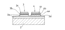
図1は,本発明における第1の実施の形態に係る2波長型半導体レーザ発光装置1を示す。 FIG. 1 shows a two-wavelength semiconductor laser light emitting device 1 according to a first embodiment of the present invention.
この半導体レーザ発光装置1は,例えばn型GaAsより成る基板2と,その上面に横に並べて配設した赤外レーザ発光素子3及び赤色レーザ発光素子4とを備えている。
The semiconductor laser light emitting device 1 includes a
前記赤外レーザ発光素子3は,前記基板2の上面に形成した例えばn型AlGaAsより成る下層クラッド層3aと,この下層クラッド層3aの上面に重ねて形成した発振波長が750〜850nmとなる組成を有する例えばAlGaAsより成る活性層3bと,この活性層3bの上面に重ねて形成した例えばp型AlGaAsより成る上層クラッド層3cと,この上層クラッド層3cの上面に,当該上面に設けたリッジ3c′の両側に例えばn型AlGaAsより成る埋め込み層3dを挟んで形成した例えばp型GaAsより成るコンタクト層3eとの積層体に構成されている。
The infrared laser
前記赤外レーザ発光素子3における下層クラッド層3aは,その厚さ方向の中間部に薄い厚さの例えばInGaPによるエッチングストップ層3a′を備えて,前記基板2における上面のうち前記赤色レーザ発光素子4の下側の部分にまで延びており,この赤外用の下層クラッド層3aは,前記赤色レーザ発光素子4の下側の部分において,当該下層クラッド層3aのうち前記エッチングストップ層3a′よりも上側の部分が,前記エッチングストップ層3a′が露出するようにエッチング処理にて除去されている。
The lower
そして,前記赤色レーザ発光素子4は,前記エッチング処理にて露出する前記エッチングストップ層3a′の上面に形成した例えばn型InGaAlPより成る下層クラッド層4aと,この下層クラッド層4aの上面に重ねて形成した発振波長が635〜680nmとなる組成を有する例えばInGaPより成る活性層4bと,この活性層4bの上面に重ねて形成した例えばp型InGaAlPより成る上層クラッド層4cと,この上層クラッド層4cの上面に,当該上面に設けたリッジ4c′の両側に例えばn型InAlP又はn型InGaAlPより成る埋め込み層4dを挟んで形成した例えばp型GaAsより成るコンタクト層4eとの積層体に構成されている。
The red laser
前記2波長型半導体レーザ発光装置1は,前記したように,前記赤外レーザ発光素子3の一部を構成する赤外用下層クラッド層3aを,当該赤外用下層クラッド層3aにおける厚さ方向の中間部にエッチングストップ層3a′を設けて,前記赤色レーザ発光素子4の部分まで延長し,この赤外用下層クラッド層3aのうち前記エッチングストップ層3a′より上側の部分を,前記赤色レーザ発光素子4の部分において前記エッチングストップ層3a′が露出するようにエッチング処理にて除去し,この部分に前記赤色レーザ発光素子4を設けるという構成であることにより,前記赤外用下層クラッド層3aのうち前記エッチングストップ層3a′より下側においてエッチング処理に対して残っている部分,つまり,前記赤外用下層クラッド層3aのうち前記エッチングストップ層3a′を含んでこれより下側の部分が,前記特許文献2における嵩上げ層と同じ作用を果たすことになるから,前記赤外レーザ発光素子3における活性層3bと,赤色レーザ発光素子4における活性層4bとを,基板2の上面から実質上同じ高さ位置に揃えることが,前記特許文献1のように,赤色レーザ発光素子における下層クラッド層の厚さを厚くしたり,前記特許文献2のように嵩上げ層を形成したりすることなく,確実に達成できる。
As described above, the two-wavelength semiconductor laser light emitting device 1 is configured such that the infrared
また,前記した構成において,前記InGaPによるエッチングストップ層3a′は,赤外用のAlGaAsによる活性層3bよりもバンドキャップが大きいために,前記エッチングストップ層3a′による赤外光の吸収・損失は少ない一方,前記エッチングストップ層3a′の下側において残る赤外用のn型AlGaAsによる下層クラッド層3aは,赤色用のInGaPによる活性層4bよりもバンドキャップが大きいために,前記赤外用の下層クラッド層3aによる赤色光の吸収・損失は少ない。
In the above-described configuration, the InGaP
次に,前記した第1の実施の形態の半導体レーザ発光装置1の製造に際しては,以下に述べる工程を備えている。 Next, when manufacturing the semiconductor laser light emitting device 1 of the first embodiment described above, the following steps are provided.
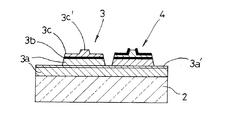
先ず,図3に示すように,基板2の上面における全体に,前記赤外用のn型AlGaAsによる下層クラッド層3aを,当該下層クラッド層3aにおける厚さ方向の中間部にInGaPによるエッチングストップ層3a′を設けて形成し,この下層クラッド層3aの上面に重ねて前記赤外用のAlGaAsによる活性層3bを形成し,この活性層3bに重ねて赤外用のp型AlGaAsによる上層クラッド層3cを形成することにより,第1積層体5を構成するという第1エピ工程を備えている。
First, as shown in FIG. 3, the lower
前記した第1エピ工程において,前記赤外用のn型AlGaAsによる下層クラッド層3aのうちその厚さ方向の中間部に前記InGaPによるエッチングストップ層3a′を設けることは,前記赤外用の下層クラッド層3aを,Al,Ga,Asの供給にて成長形成する途中において,例えば,前記Al及びAsの供給を止めてIn及びPを供給することを適宜時間だけ行うように操作することによって達成できる。
In the first epi step, the InGaP
また,前記エッチングストップ層3a′は,前記n型AlGaAsによる下層クラッド層3aを成長形成する途中において,その成膜原材料の混合比を,適宜時間の間だけ代えることによっても形成することができる。
The
次に,前記第1積層体5に対して,当該第1積層体5のうち前記赤外レーザ発光素子3に該当する部分をマスキングした状態で,この第1積層体5をエッチング溶液にて除去するという第1エッチング工程を備えている。
Next, the first
この第1エッチング工程により,前記第1積層体5において,前記マスキングしていない部分のうちエッチングストップ層3a′より上側の部分は,図4に示すように,前記マスキングした部分を残して除去されることになる。
By this first etching step, the portion of the
これにより,前記赤外レーザ発光素子3を,その下層クラッド層3aのうち前記エッチングストップ層3a′より下側の部分を前記赤色レーザ発光素子4の下側において残した形態にして形成することができる。
Thus, the infrared laser
この第1エッチング工程により,前記エッチングストップ層3a′は,前記赤色レーザ発光素子4の部分において露出することになる。
By this first etching step, the
この場合において,前記エッチングストップ層3a′にアルミニウムを含んでいるときには,前記第1エッチング工程にて露出した前記エッチングストップ層3a′の表面に,アルミニウムの酸化被膜が発生することになるが,前記エッチングストップ層3a′を,例えば,前記したようにInGaPにするように,アルミニウムを含まない材料にて形成することにより,前記第1エッチング工程によって露出した前記エッチングストップ層3a′の表面に,アルミニウム等の金属の酸化被膜ができることを確実に抑制できるから,前記第1エッチング工程に次いで後述する赤色用の下層クラッド層4aを形成するに先立って,前記エッチングストップ層3a′の表面における酸化被膜を除去したり,前記酸化被膜による悪影響を避けるためのバッファー層を形成したりする処理を行う必要がなく,前記第1エッチング工程に引き続いて前記赤色用の下層クラッド層4aを形成することができる。
In this case, when the
次に,図5に示すように,前記赤外レーザ発光素子3及び前記エッチングストップ層3a′の上面の全体に,前記赤色用のn型InGaAlPによる下層クラッド層4aを形成し,この下層クラッド層4aの上面に重ねて前記赤色用のInGaPによる活性層4bを形成し,この活性層4bに重ねて赤色用のp型InGaAlPによる上層クラッド層4cを形成することにより,第2積層体6を構成するという第2エピ工程を備えている。
Next, as shown in FIG. 5, a lower
次に,前記第2積層体6に対して,当該第2積層体6のうち前記赤色レーザ発光素子4に該当する部分をマスキングした状態で,この第2積層体6をエッチング溶液にて除去するという第2エッチング工程を備えている。
Next, the second stacked body 6 is removed with an etching solution in a state where the portion of the second stacked body 6 corresponding to the red laser
この第2エッチング工程により,前記第2積層体6のうち前記マスキングしていない部分が除去されることになるから,図6に示すように,前記エッチングストップ層3a′の上面に,前記赤色レーザ発光素子4を形成することができる。
In this second etching step, the unmasked portion of the second stacked body 6 is removed. Therefore, as shown in FIG. 6, the red laser is formed on the upper surface of the
本発明においては,前記に加えて,前記赤色レーザ発光素子4における上層クラッド層4cの上面に,図7に示すように,リッジ4c′を設ける工程を経たのち,図8に示すように,埋め込み層4dを形成するエピ工程を備えている。
In the present invention, in addition to the above, after a step of providing a
次に,前記赤外レーザ発光素子3における上層クラッド層3cの上面に,図9に示すように,リッジ3c′を設ける工程を経たのち,図10に示すように,埋め込み層3dを形成するエピ工程を備えている。
Next, after the step of providing a
そして,前記赤外レーザ発光素子3及び赤色レーザ発光素子4の各々に対してコンタクト層3e,4eを形成するエピ工程を備えており,これらの各工程を経ることにより,前記図1に示す構造の半導体レーザ発光装置1を製造することができる。
An epi process for forming
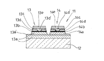
次に,図2は,第2の実施の形態による2波長型半導体レーザ発光装置11を示す。この第2の実施の形態による半導体レーザ発光装置11は,例えばn型GaAsより成る基板12と,その上面に横に並べて配設した赤外レーザ発光素子3及び赤色レーザ発光素子4とを備えている。
Next, FIG. 2 shows a two-wavelength semiconductor laser
前記赤外レーザ発光素子13は,前記基板12の上面に形成した例えばn型AlGaAsより成る下層クラッド層13aと,この下層クラッド層13aの上面に重ねて形成した発振波長が750〜850nmとなる組成を有する例えばAlGaAsより成る活性層13bと,この活性層13bの上面にリッジ13d′を設けて形成した例えばn型AlGaAsより成る埋め込み層13dと,この埋め込み層13dの上面に,当該埋め込み層13dにおけるリッジ13d′の箇所において前記活性層13bに直接重なるように形成した例えばp型AlGaAsより成る上層クラッド層3cと,この上層クラッド層3cの上面に形成した例えばp型GaAsより成るコンタクト層13eとの積層体に構成されている。
The infrared laser
前記赤外レーザ発光素子13における下層クラッド層13aは,その厚さ方向の中間部に薄い厚さの例えばInGaPによるエッチングストップ層13a′を備えて,前記基板12における上面のうち前記赤色レーザ発光素子14の下側の部分にまで延びおり,この赤外用の下層クラッド層13aは,前記赤色レーザ発光素子14の下側の部分において,当該下層クラッド層13aのうち前記エッチングストップ層13a′よりも上側の部分が,前記エッチングストップ層13a′が露出するようにエッチング処理にて除去されている。
The lower
そして,前記赤色レーザ発光素子14は,前記エッチング処理にて露出する前記エッチングストップ層13a′の上面に形成した例えばn型InGaAlPより成る下層クラッド層14aと,この下層クラッド層14aの上面に重ねて形成した発振波長が635〜680nmとなる組成を有する例えばInGaPより成る活性層14bと,この活性層14bの上面にリッジ14d′を設けて形成した例えばn型InAlP又はn型InGaAlPより成る埋め込み層14dと,この埋め込み層14dの上面に,当該埋め込み層14dにおけるリッジ14d′の箇所において前記活性層14bに直接重なるように形成した例えばp型InGaAlPより成る上層クラッド層14cと,この上層クラッド層14cの上面に形成した例えばp型GaAsより成るコンタクト層14eとの積層体に構成されている。
The red laser
この第2の実施の形態による2波長型半導体レーザ発光装置11は,前記第1の実施の形態による2波長型半導体レーザ発光装置1と同様に,前記赤外レーザ発光素子13の一部を構成する赤外用下層クラッド層13aを,当該赤外用下層クラッド層13aにおける厚さ方向の中間部にエッチングストップ層13a′を設けて,前記赤色レーザ発光素子14の部分まで延長し,この赤外用下層クラッド層13aのうち前記エッチングストップ層13a′より上側の部分を,前記赤色レーザ発光素子14の部分において前記エッチングストップ層13a′が露出するようにエッチング処理にて除去し,この部分に前記赤色レーザ発光素子14を設けるという構成であることにより,前記第1の実施の形態による2波長型半導体レーザ発光装置1と同様の効果を有するとともに,前記第1の実施の形態による2波長型半導体レーザ発光装置1と同様の方法で製造することができる。
The two-wavelength semiconductor laser light-emitting
1,11 半導体レーザ発光装置
2,12 基板
3,13 赤外レーザ発光素子
3a,13a 下層クラッド層
3a′,13a′ エッチングストップ層
3b,13b 活性層
3c,13c 上層クラッド層
4,14 赤色レーザ発光素子
4a,14a 下層クラッド層
4b,14b 活性層
4c,14c 上層クラッド層
5 第1積層体
6 第2積層体
DESCRIPTION OF
Claims (4)
前記赤外用の下層クラッド層を,当該下層クラッド層における厚さ方向の中間部にエッチングストップ層を設けて,前記赤色レーザ発光素子の部分まで延長し,この赤外用の下層クラッド層のうち前記エッチングストップ層より上側の部分を,前記赤色レーザ発光素子の部分において前記エッチングストップ層が露出するようにエッチング処理にて除去し,この部分に前記赤色レーザ発光素子を設け,更に,前記赤外レーザ発光素子における上層クラッド層に,リッジを形成するとともに,このリッジを囲む埋め込み層を設ける一方,前記赤色レーザ発光素子における上層クラッド層に,リッジを形成するとともに,このリッジを囲む埋め込み層を設けることを特徴とする2波長型半導体レーザ発光装置。 An infrared laser light emitting device in which an infrared lower clad layer, an active layer and an upper clad layer are laminated on the upper surface of one substrate, and a red laser light emitting device in which a red lower clad layer, an active layer and an upper clad layer are laminated. In a two-wavelength semiconductor laser light emitting device,
The infrared lower cladding layer is extended to the red laser light emitting element portion by providing an etching stop layer in the middle in the thickness direction of the lower cladding layer, and the etching is performed on the infrared lower cladding layer. The portion above the stop layer is removed by an etching process so that the etching stop layer is exposed in the portion of the red laser light emitting device, the red laser light emitting device is provided in this portion, and the infrared laser light emission is further performed. A ridge is formed in the upper clad layer of the device, and a buried layer surrounding the ridge is provided. On the other hand, a ridge is formed in the upper clad layer in the red laser light emitting device, and a buried layer surrounding the ridge is provided . A two-wavelength semiconductor laser light emitting device characterized by the above.
前記基板の上面に,赤外用の下層クラッド層,活性層及び上層クラッド層を有する第1積層体を設ける第1エピ工程と,この第1積層体の一部に前記赤外レーザ発光素子を残しこれ以外の部分を除去する第1エッチング工程とを備え,
前記下層クラッド層の形成する工程が,当該下層クラッド層の厚さ方向の中間部に前記第1エッチング工程では除去されないエッチングストップ層を設ける工程を含み,
前記第1エッチング工程が前記エッチングストップ層より上側の部分を前記エッチングストップ層が露出するように除去する工程であり,
更に,前記赤外レーザ発光素子及び前記エッチングストップ層の上面に,赤色用の下層クラッド層,活性層及び上層クラッド層から成る第2積層体を設ける第2エピ工程と,この第2積層体の一部に前記赤色レーザ発光素子を残しこれ以外の部分を除去する第2エッチング工程とを備えており,
更に,前記赤外レーザ発光素子における上層クラッド層に,リッジを形成するとともに,このリッジを囲む埋め込み層を形成する工程と,前記赤色レーザ発光素子における上層クラッド層に,リッジを形成するとともに,このリッジを囲む埋め込み層を形成する工程とを,
備えていることを特徴とする2波長型半導体レーザ発光装置の製造方法。 In a method of manufacturing a two-wavelength type semiconductor laser light emitting device comprising an infrared laser light emitting element and a red laser light emitting element arranged side by side on an upper surface of a single substrate,
A first epitaxial step of providing a first laminate having an infrared lower clad layer, an active layer and an upper clad layer on the upper surface of the substrate; and leaving the infrared laser emitting element in a part of the first laminate. A first etching step for removing portions other than this ,
The step of forming the lower cladding layer includes a step of providing an etching stop layer that is not removed in the first etching step in an intermediate portion in the thickness direction of the lower cladding layer;
The first etching step is a step of removing a portion above the etching stop layer so that the etching stop layer is exposed;
Furthermore, a second epi step of providing a second laminated body composed of a lower layer cladding layer for red, an active layer and an upper layer cladding layer on the upper surface of the infrared laser light emitting element and the etching stop layer; and A second etching step for leaving the red laser light emitting element in part and removing the other part,
Further, a step of forming a ridge in the upper clad layer in the infrared laser light emitting device and a buried layer surrounding the ridge, and a step of forming a ridge in the upper clad layer in the red laser light emitting device, Forming a buried layer surrounding the ridge ,
A method of manufacturing a two-wavelength semiconductor laser light-emitting device.
Priority Applications (7)
| Application Number | Priority Date | Filing Date | Title |
|---|---|---|---|
| JP2005307194A JP5013698B2 (en) | 2005-10-21 | 2005-10-21 | Dual wavelength semiconductor laser light emitting device and method for manufacturing the same |
| KR1020087010171A KR101006267B1 (en) | 2005-10-21 | 2006-10-16 | Semiconductor laser light emitting device and method for manufacturing same |
| US12/083,913 US7860138B2 (en) | 2005-10-21 | 2006-10-16 | Semiconductor laser light emitting device and method for manufacturing same |
| CN2006800389155A CN101292402B (en) | 2005-10-21 | 2006-10-16 | Semiconductor laser light emitting device and method for manufacturing same |
| PCT/JP2006/320538 WO2007046317A1 (en) | 2005-10-21 | 2006-10-16 | Semiconductor laser light emitting device and method for manufacturing same |
| TW095138591A TW200721619A (en) | 2005-10-21 | 2006-10-19 | Semiconductor laser light emitting device and method for manufacturing the same |
| US12/949,327 US8102892B2 (en) | 2005-10-21 | 2010-11-18 | Semiconductor laser light emitting device and method for manufacturing same |
Applications Claiming Priority (1)
| Application Number | Priority Date | Filing Date | Title |
|---|---|---|---|
| JP2005307194A JP5013698B2 (en) | 2005-10-21 | 2005-10-21 | Dual wavelength semiconductor laser light emitting device and method for manufacturing the same |
Publications (2)
| Publication Number | Publication Date |
|---|---|
| JP2007115974A JP2007115974A (en) | 2007-05-10 |
| JP5013698B2 true JP5013698B2 (en) | 2012-08-29 |
Family
ID=37962411
Family Applications (1)
| Application Number | Title | Priority Date | Filing Date |
|---|---|---|---|
| JP2005307194A Active JP5013698B2 (en) | 2005-10-21 | 2005-10-21 | Dual wavelength semiconductor laser light emitting device and method for manufacturing the same |
Country Status (6)
| Country | Link |
|---|---|
| US (2) | US7860138B2 (en) |
| JP (1) | JP5013698B2 (en) |
| KR (1) | KR101006267B1 (en) |
| CN (1) | CN101292402B (en) |
| TW (1) | TW200721619A (en) |
| WO (1) | WO2007046317A1 (en) |
Families Citing this family (3)
| Publication number | Priority date | Publication date | Assignee | Title |
|---|---|---|---|---|
| JP5485905B2 (en) * | 2008-10-31 | 2014-05-07 | オプトエナジー株式会社 | Semiconductor laser element |
| US9865772B2 (en) | 2015-01-06 | 2018-01-09 | Apple Inc. | LED structures for reduced non-radiative sidewall recombination |
| JP7248152B2 (en) * | 2020-01-22 | 2023-03-29 | 三菱電機株式会社 | Semiconductor device and method for manufacturing semiconductor device |
Family Cites Families (17)
| Publication number | Priority date | Publication date | Assignee | Title |
|---|---|---|---|---|
| US4961197A (en) * | 1988-09-07 | 1990-10-02 | Hitachi, Ltd. | Semiconductor laser device |
| JPH0590699A (en) * | 1991-09-27 | 1993-04-09 | Olympus Optical Co Ltd | Manufacture of multiple-wavelength semiconductor laser device |
| US5412678A (en) * | 1992-09-22 | 1995-05-02 | Xerox Corporation | Multi-beam, orthogonally-polarized emitting monolithic quantum well lasers |
| US5396508A (en) | 1992-09-22 | 1995-03-07 | Xerox Corporation | Polarization switchable quantum well laser |
| JPH1098234A (en) * | 1996-09-25 | 1998-04-14 | Mitsubishi Electric Corp | Semiconductor laser and its manufacture |
| JP2000307191A (en) * | 1999-04-22 | 2000-11-02 | Victor Co Of Japan Ltd | Manufacture of semiconductor laser device |
| US6400743B1 (en) * | 1999-08-05 | 2002-06-04 | Fuji Photo Film Co., Ltd. | High-power semiconductor laser device having current confinement structure and index-guided structure |
| JP3950590B2 (en) | 1999-08-31 | 2007-08-01 | ローム株式会社 | Semiconductor laser and manufacturing method thereof |
| JP3971566B2 (en) * | 1999-11-25 | 2007-09-05 | 松下電器産業株式会社 | Semiconductor laser device and manufacturing method thereof |
| US6813290B1 (en) * | 1999-11-25 | 2004-11-02 | Matsushita Electric Industrial Co., Ltd. | Semiconductor laser device and method for fabricating the same |
| US6396508B1 (en) * | 1999-12-02 | 2002-05-28 | Matsushita Electronics Corp. | Dynamic low-level enhancement and reduction of moving picture disturbance for a digital display |
| US6546035B2 (en) | 2000-02-29 | 2003-04-08 | Matsushita Electric Industrial Co., Ltd. | Semiconductor laser diode array and method of fabricating the same |
| JP3971581B2 (en) | 2000-02-29 | 2007-09-05 | 松下電器産業株式会社 | Semiconductor laser element array and manufacturing method thereof |
| JP2001244569A (en) | 2000-03-01 | 2001-09-07 | Sony Corp | Method of manufacturing for semiconductor laser light emitting device |
| JP2002368335A (en) * | 2001-06-05 | 2002-12-20 | Ricoh Co Ltd | Semiconductor laser element, its manufacturing method, semiconductor laser array, optical communication system, optical interconnection system, optical pickup system, and electrophotographic system |
| JP2004186259A (en) * | 2002-11-29 | 2004-07-02 | Toshiba Corp | Semiconductor laser device, its manufacturing method, and multiwavelength integrated semiconductor laser apparatus |
| JP4326297B2 (en) * | 2003-09-30 | 2009-09-02 | シャープ株式会社 | Monolithic multi-wavelength laser element and manufacturing method thereof |
-
2005
- 2005-10-21 JP JP2005307194A patent/JP5013698B2/en active Active
-
2006
- 2006-10-16 US US12/083,913 patent/US7860138B2/en active Active
- 2006-10-16 WO PCT/JP2006/320538 patent/WO2007046317A1/en active Application Filing
- 2006-10-16 KR KR1020087010171A patent/KR101006267B1/en active IP Right Grant
- 2006-10-16 CN CN2006800389155A patent/CN101292402B/en active Active
- 2006-10-19 TW TW095138591A patent/TW200721619A/en unknown
-
2010
- 2010-11-18 US US12/949,327 patent/US8102892B2/en active Active
Also Published As
| Publication number | Publication date |
|---|---|
| WO2007046317A1 (en) | 2007-04-26 |
| US7860138B2 (en) | 2010-12-28 |
| US20110064104A1 (en) | 2011-03-17 |
| US20090168824A1 (en) | 2009-07-02 |
| JP2007115974A (en) | 2007-05-10 |
| TW200721619A (en) | 2007-06-01 |
| US8102892B2 (en) | 2012-01-24 |
| KR101006267B1 (en) | 2011-01-06 |
| TWI310255B (en) | 2009-05-21 |
| CN101292402B (en) | 2010-05-19 |
| KR20080061384A (en) | 2008-07-02 |
| CN101292402A (en) | 2008-10-22 |
Similar Documents
| Publication | Publication Date | Title |
|---|---|---|
| US6794688B2 (en) | Semiconductor light-emitting device and manufacturing method therefor, and LED lamp and LED display | |
| JPH0690063A (en) | Semiconductor laser | |
| WO2007097411A1 (en) | Double wavelength semiconductor light emitting device and method for manufacturing same | |
| JP4332407B2 (en) | Semiconductor light emitting device and manufacturing method thereof | |
| JP2008047684A (en) | Semiconductor luminescent element, manufacturing method thereof, and semiconductor luminescent device | |
| JP2007067198A (en) | Light emitting element | |
| US20030010989A1 (en) | Light-emitting diode array | |
| US20110243171A1 (en) | Nitride-based semiconductor laser device | |
| CN1320712C (en) | Semiconductor laser device and manufacturing method therefor | |
| JP5013698B2 (en) | Dual wavelength semiconductor laser light emitting device and method for manufacturing the same | |
| JP5264935B2 (en) | Optoelectronic component and manufacturing method thereof | |
| JP2003110135A5 (en) | ||
| JP2010062201A (en) | Semiconductor light emitting element and method of manufacturing the same | |
| JP5277066B2 (en) | Semiconductor light emitting device and manufacturing method thereof | |
| JP2012160665A (en) | Semiconductor light emitting device | |
| JP2008021845A (en) | Semiconductor light emitting device, and its manufacturing method | |
| JP3332785B2 (en) | Semiconductor light emitting device and method of manufacturing the same | |
| CN100426608C (en) | Semiconductor laser device | |
| JP2014192514A (en) | Method for manufacturing group iii nitride semiconductor light emitting element | |
| JP3950590B2 (en) | Semiconductor laser and manufacturing method thereof | |
| JP2006270073A (en) | Light-emitting diode and method of manufacturing it | |
| JP2007150075A (en) | Nitride semiconductor light emitting element | |
| JP2009152240A (en) | Semiconductor light-emitting element and method of manufacturing the same | |
| JP4804261B2 (en) | Semiconductor optical device manufacturing method and semiconductor optical device semiconductor substrate | |
| JP2006351784A (en) | Semiconductor laser and its manufacturing method |
Legal Events
| Date | Code | Title | Description |
|---|---|---|---|
| A621 | Written request for application examination |
Free format text: JAPANESE INTERMEDIATE CODE: A621 Effective date: 20080909 |
|
| A131 | Notification of reasons for refusal |
Free format text: JAPANESE INTERMEDIATE CODE: A131 Effective date: 20111011 |
|
| TRDD | Decision of grant or rejection written | ||
| A01 | Written decision to grant a patent or to grant a registration (utility model) |
Free format text: JAPANESE INTERMEDIATE CODE: A01 Effective date: 20120516 |
|
| A01 | Written decision to grant a patent or to grant a registration (utility model) |
Free format text: JAPANESE INTERMEDIATE CODE: A01 |
|
| A61 | First payment of annual fees (during grant procedure) |
Free format text: JAPANESE INTERMEDIATE CODE: A61 Effective date: 20120605 |
|
| FPAY | Renewal fee payment (event date is renewal date of database) |
Free format text: PAYMENT UNTIL: 20150615 Year of fee payment: 3 |
|
| R150 | Certificate of patent or registration of utility model |
Free format text: JAPANESE INTERMEDIATE CODE: R150 Ref document number: 5013698 Country of ref document: JP Free format text: JAPANESE INTERMEDIATE CODE: R150 |
|
| R250 | Receipt of annual fees |
Free format text: JAPANESE INTERMEDIATE CODE: R250 |
|
| R250 | Receipt of annual fees |
Free format text: JAPANESE INTERMEDIATE CODE: R250 |
|
| R250 | Receipt of annual fees |
Free format text: JAPANESE INTERMEDIATE CODE: R250 |
|
| R250 | Receipt of annual fees |
Free format text: JAPANESE INTERMEDIATE CODE: R250 |
|
| R250 | Receipt of annual fees |
Free format text: JAPANESE INTERMEDIATE CODE: R250 |