JP5008384B2 - Semiconductor device - Google Patents
Semiconductor device Download PDFInfo
- Publication number
- JP5008384B2 JP5008384B2 JP2006321981A JP2006321981A JP5008384B2 JP 5008384 B2 JP5008384 B2 JP 5008384B2 JP 2006321981 A JP2006321981 A JP 2006321981A JP 2006321981 A JP2006321981 A JP 2006321981A JP 5008384 B2 JP5008384 B2 JP 5008384B2
- Authority
- JP
- Japan
- Prior art keywords
- circuit
- chip
- routine
- signal
- collision
- Prior art date
- Legal status (The legal status is an assumption and is not a legal conclusion. Google has not performed a legal analysis and makes no representation as to the accuracy of the status listed.)
- Expired - Fee Related
Links
Images


Description
本発明は半導体装置に関する。本発明は特に外部との信号の送受信を行う半導体装置、所謂RFID(Radio Frequency Identification)用ICチップ(IDチップ、ICタグ、IDタグ、RFタグ、無線タグ、電子タグ、トランスポンダともいう)に関する。 The present invention relates to a semiconductor device. The present invention particularly relates to a semiconductor device that performs transmission / reception of signals to / from the outside, that is, a so-called RFID (Radio Frequency Identification) IC chip (also referred to as an ID chip, IC tag, ID tag, RF tag, wireless tag, electronic tag, or transponder).
なお、ここでいう半導体装置とは、半導体特性を利用することで機能しうる装置全般を指すものとする。 Note that the semiconductor device here refers to all devices that can function by utilizing semiconductor characteristics.
コンピュータ技術の発展や、画像認識技術の向上によって、バーコードなどの媒体を用いた情報認識が広く普及し、商品データの認識などに用いられている。今後はさらに多量の情報認識が実施されると予想される。その一方、バーコードによる情報読み取りなどでは、バーコードリーダーがバーコードとの接触を必要とすることや、バーコードに記録される情報量があまり多くできないという欠点があり、非接触の情報認識および媒体の記憶容量増大が望まれている。 Due to the development of computer technology and the improvement of image recognition technology, information recognition using a medium such as a barcode has become widespread and used for product data recognition and the like. In the future, it is expected that more information will be recognized. On the other hand, when reading information using barcodes, there are drawbacks that the barcode reader requires contact with the barcode and that the amount of information recorded on the barcode cannot be very large. It is desired to increase the storage capacity of the medium.
このような要望から、非接触型のRFID用ICチップ(以下、ICチップという)、及びリーダ/ライタ装置(質問器ともいう;以下、リーダライタという)が開発されている。ICチップとはICチップ内のメモリ回路に必要な情報を記憶し、非接触手段、一般的には無線手段を用い、リーダライタにより内部の情報を読み取るものである。このようなICチップに記憶された情報を読み取る情報処理装置の実用化によって、商品流通などの簡素化、低コスト化、高いセキュリティの確保が可能になるものと期待されている。 In view of such a demand, a contactless RFID IC chip (hereinafter referred to as an IC chip) and a reader / writer device (also referred to as an interrogator; hereinafter referred to as a reader / writer) have been developed. An IC chip stores necessary information in a memory circuit in the IC chip, and uses non-contact means, generally wireless means, to read internal information by a reader / writer. The practical application of an information processing apparatus that reads information stored in such an IC chip is expected to simplify product distribution, reduce costs, and ensure high security.
近年、有価証券、商品の管理など、自動認識が必要なあらゆる分野を対象に、非接触でデータの授受が行える普及が始まっている。このようなICチップを搭載したカードは、データの授受を行う際に使用する周波数帯に適応した形状のアンテナを介して、外部の機器と非接触でデータの読み書きをするようになされる。 In recent years, the spread of contactless data transmission and reception has started for all fields that require automatic recognition, such as securities and product management. A card equipped with such an IC chip reads and writes data without contact with an external device via an antenna having a shape adapted to a frequency band used when data is exchanged.
ICチップなどの半導体装置はバーコード等の2次元の情報の読み取りとは異なり、リーダライタにアンチコリジョン機能(衝突防止機能、または単にアンチコリジョンともいう)を備えることによって、複数のICチップからの信号を読み取ることができる(例えば、ISO15693−3の規格に準ずるALOHA方式)。また、ICチップ内において、複数の回路を備えることによって、アンチコリジョン機能の動作を行う方法がある。特許文献1によると、共振用コンデンサを複数設け、共振周波数の値を一定に保つようにすることで、ICチップ間のアンチコリジョン対応機能を確実に行うことができるデータ処理方法について開示されている。
しかしながら、上記特許文献に記載のアンチコリジョンを行うデータ処理方法では、ICチップ上にトランジスタで構成される回路で論理回路を構成する。そのため、製品毎の無線手段の信号の種類や、規格が変更になることに伴う仕様の変更により、ICチップのマスク設計の段階から作り直す必要があった。しかしながら、ICチップを再度作り直すことは、製造コストの増加及び製造時間の遅滞を招き、再度作り直したICチップが不具合をおこした場合には、さらに製造コストの増加及び製造時間の遅滞を招くことが懸念される。 However, in the data processing method for performing anti-collision described in the above-mentioned patent document, a logic circuit is configured by a circuit configured by transistors on an IC chip. For this reason, it is necessary to recreate the IC chip mask from the stage of design due to the change in the type of signal of the wireless means for each product and the change in specifications accompanying the change in the standard. However, re-creating the IC chip causes an increase in manufacturing cost and a delay in manufacturing time, and if the re-created IC chip has a problem, it further increases the manufacturing cost and delays in the manufacturing time. Concerned.
そこで本発明は、ICチップの製造中や製造後に、製品毎の無線手段の信号の種類や規格が変更になることに伴う仕様の変更であっても、半導体装置内に格納されたプログラムの変更だけでアンチコリジョン機能を有する半導体装置を提供することを課題とする。 Therefore, the present invention changes the program stored in the semiconductor device even if the specification changes due to the change in the signal type or standard of the wireless means for each product during or after the manufacture of the IC chip. It is an object to provide a semiconductor device having an anti-collision function.
上記課題を鑑み本発明は、アンチコリジョンを行う半導体装置として、半導体装置内にROM、RAM、CPU等の記憶素子及び演算素子を設け、外部への送信信号または外部からの受信信号がコリジョン状態(衝突状態)になった際に記憶素子に格納されたアンチコリジョンプログラムを読み出す。そして、アンチコリジョンプログラムはアンチコリジョンルーチンにより構成され、演算素子及び記憶素子によって、アンチコリジョンルーチンを実行することを特徴とする。なお、半導体装置としては、無線通信可能なICチップが挙げられる。 In view of the above problems, according to the present invention, a semiconductor device that performs anti-collision is provided with a storage element and an arithmetic element such as a ROM, a RAM, and a CPU, and a transmission signal to the outside or a reception signal from the outside is in a collision state ( The anti-collision program stored in the storage element is read out when the collision state occurs. The anti-collision program is constituted by an anti-collision routine, and the anti-collision routine is executed by an arithmetic element and a storage element. Note that an IC chip capable of wireless communication is given as the semiconductor device.
以下に本発明の具体的な構成を示す。 The specific configuration of the present invention is shown below.
本発明の半導体装置の一は、演算回路、及び外部との信号の送受信を行うための回路を有し、前記演算回路は中央処理装置、ランダムアクセスメモリ、読み出し専用メモリ、及びコントローラを有し、前記読み出し専用メモリは、前記外部との信号の送受信における衝突防止処理を行うためのプログラムが記憶されており、前記プログラムが前記中央処理装置において実行されることで、前記演算回路は衝突防止処理を行う構成とした。 One of the semiconductor devices of the present invention includes an arithmetic circuit and a circuit for performing transmission and reception of signals with the outside, and the arithmetic circuit includes a central processing unit, a random access memory, a read-only memory, and a controller, The read-only memory stores a program for performing a collision prevention process in signal transmission / reception with the outside, and the arithmetic circuit performs the collision prevention process by executing the program in the central processing unit. The configuration is to be performed.
また、別の本発明の半導体装置の一は、演算回路、及び外部との信号の送受信を行うための回路を有し、前記演算回路は中央処理装置、ランダムアクセスメモリ、読み出し専用メモリ、及びコントローラを有し、前記読み出し専用メモリは、前記外部との信号の送受信における衝突防止処理を行うためのプログラムが記憶されており、前記プログラムが複数のルーチンで構成され、当該複数のルーチンが前記中央処理装置において処理されることで、前記演算回路は衝突防止処理を行う構成とした。 Another semiconductor device of the present invention includes an arithmetic circuit and a circuit for transmitting and receiving signals to and from the outside. The arithmetic circuit includes a central processing unit, a random access memory, a read-only memory, and a controller. The read-only memory stores a program for performing collision prevention processing in signal transmission / reception with the outside, and the program includes a plurality of routines, and the plurality of routines are the central processing. The arithmetic circuit is configured to perform a collision prevention process by being processed in the apparatus.
また、別の本発明の半導体装置の一は、演算回路、補助演算回路、及び外部との信号の送受信を行うための回路を有し、前記演算回路は中央処理装置、ランダムアクセスメモリ、読み出し専用メモリ、及びコントローラを有し、前記読み出し専用メモリは、前記外部との信号の送受信における衝突防止処理を行うためのプログラムが記憶されており、前記プログラムが複数のルーチンで構成され、当該複数のルーチンが前記中央処理装置において処理されること及び前記補助演算回路で処理されることで、前記演算回路は衝突防止処理を行う構成とした。 Another semiconductor device of the present invention includes an arithmetic circuit, an auxiliary arithmetic circuit, and a circuit for transmitting and receiving signals to and from the outside. The arithmetic circuit includes a central processing unit, a random access memory, and a read-only memory. The read-only memory has a memory and a controller, and stores a program for performing a collision prevention process in signal transmission / reception with the outside. The program includes a plurality of routines, and the plurality of routines Are processed by the central processing unit and processed by the auxiliary arithmetic circuit, so that the arithmetic circuit performs a collision prevention process.
また、別の本発明の半導体装置の一は、演算回路、及び外部との信号の送受信を行うための回路を有し、前記演算回路は中央処理装置、ランダムアクセスメモリ、読み出し専用メモリ、及びコントローラを有し、前記読み出し専用メモリは、前記外部との信号の送受信における衝突防止処理を行うためのプログラムが記憶されており、前記プログラムが、前記外部からの信号のフラグ、コマンドを判断する第1のルーチンと、前記コントローラのマスク長コードを判断する第2のルーチンと、前記外部からの信号の巡回冗長検査を判断する第3のルーチンと、前記外部からの信号のスロットを判断する第4のルーチンと、で構成され、当該第1乃至第4のルーチンが前記中央処理装置において処理されることで、前記演算回路は衝突防止処理を行う構成とした。 Another semiconductor device of the present invention includes an arithmetic circuit and a circuit for transmitting and receiving signals to and from the outside. The arithmetic circuit includes a central processing unit, a random access memory, a read-only memory, and a controller. The read-only memory stores a program for performing a collision prevention process in signal transmission / reception with the outside, and the program determines a flag and a command of the signal from the outside. A second routine for determining the mask length code of the controller, a third routine for determining a cyclic redundancy check of the external signal, and a fourth routine for determining the slot of the external signal And the first to fourth routines are processed in the central processing unit, so that the arithmetic circuit performs a collision prevention process. It was configured to perform.
また、別の本発明の半導体装置の一は、演算回路、補助演算回路、及び外部との信号の送受信を行うための回路を有し、前記演算回路は中央処理装置、ランダムアクセスメモリ、読み出し専用メモリ、及びコントローラを有し、前記読み出し専用メモリは、前記外部との信号の送受信における衝突防止処理を行うためのプログラムが記憶されており、前記プログラムが、前記外部からの信号のフラグ、コマンドを判断する第1のルーチンと、前記コントローラのマスク長コードを判断する第2のルーチンと、前記外部からの信号の巡回冗長検査を判断する第3のルーチンと、前記外部からの信号のスロットを判断する第4のルーチンと、で構成され、前記第1乃至第4のルーチンが前記中央処理装置において処理されること及び前記補助演算回路で処理されることで、前記演算回路は衝突防止処理を行う構成とした。 Another semiconductor device of the present invention includes an arithmetic circuit, an auxiliary arithmetic circuit, and a circuit for transmitting and receiving signals to and from the outside. The arithmetic circuit includes a central processing unit, a random access memory, and a read-only memory. The read-only memory has a memory and a controller, and stores a program for performing a collision prevention process in signal transmission / reception with the outside, and the program stores a flag and a command of the signal from the outside. A first routine for determining; a second routine for determining a mask length code of the controller; a third routine for determining a cyclic redundancy check of the external signal; and determining a slot of the external signal A fourth routine, wherein the first to fourth routines are processed in the central processing unit and the auxiliary calculation By being processed by the road, the arithmetic circuit was configured to perform anti-collision processing.
また本発明において、前記第3のルーチンは前記補助演算回路で処理される構成であってもよい。 In the present invention, the third routine may be processed by the auxiliary arithmetic circuit.
また本発明において、前記外部からの信号はフレームの開始、フラグ、コマンド、データ、巡回冗長検査、フレームの終了のコードを有する構成であってもよい。 In the present invention, the external signal may include a frame start code, a flag, a command, data, a cyclic redundancy check, and a frame end code.
また本発明において、前記コントローラはCPUインターフェース、制御レジスタ、コード抽出回路、符号化回路を有する構成であってもよい。 In the present invention, the controller may have a CPU interface, a control register, a code extraction circuit, and an encoding circuit.
また本発明において、前記制御レジスタは、前記フレームの開始のコードを判断して前記衝突防止処理を行うプログラムが実行される構成であってもよい。 In the present invention, the control register may be configured to execute a program for determining the start code of the frame and performing the collision prevention process.
また本発明において、前記外部との信号の送受信を行うための回路は、アンテナ、共振回路、電源回路、リセット回路、クロック生成回路、復調回路、変調回路、及び電源回路を有する構成であってもよい。 In the present invention, the circuit for transmitting / receiving a signal to / from the outside may include an antenna, a resonance circuit, a power supply circuit, a reset circuit, a clock generation circuit, a demodulation circuit, a modulation circuit, and a power supply circuit. Good.
本発明によって、衝突防止機能を有するICチップにおいて、製品毎の無線手段の信号の種類や、規格が変更になることに伴う仕様の変更により、ICチップのマスク設計の段階から作り直す必要ない。そのため、製造コストの削減及び製造時間の短縮ができる。また、マスク設計の変更によって再度作り直したICチップが不具合といった懸念もない。 According to the present invention, in an IC chip having a collision prevention function, it is not necessary to recreate the IC chip from the mask design stage by changing the type of wireless means signal for each product or by changing specifications associated with a change in standard. Therefore, it is possible to reduce the manufacturing cost and the manufacturing time. Further, there is no concern that the IC chip remade by changing the mask design is defective.
また従来においては、専用の衝突防止機能を有するICチップを製造する際においては、衝突防止機能を備えた回路を搭載することもあった。しかしながら、本発明では、衝突防止機能を読み出し専用メモリにプログラムとして格納することにより、衝突防止機能を備えた回路より読み出し専用メモリの方が作りやすいことによるICチップの不具合の削減を図ることができる。 Conventionally, when an IC chip having a dedicated collision prevention function is manufactured, a circuit having a collision prevention function is sometimes mounted. However, in the present invention, by storing the collision prevention function as a program in the read-only memory, it is possible to reduce the defects of the IC chip due to the fact that the read-only memory is easier to make than the circuit having the collision prevention function. .
以下に、本発明の実施の形態を図面に基づいて説明する。但し、本発明は多くの異なる態様で実施することが可能であり、本発明の趣旨及びその範囲から逸脱することなくその形態及び詳細を様々に変更し得ることは当業者であれば容易に理解される。従って、本実施の形態の記載内容に限定して解釈されるものではない。なお、実施の形態を説明するための全図において、同一部分又は同様な機能を有する部分には同一の符号を付し、その繰り返しの説明は省略する。
(実施の形態1)
Embodiments of the present invention will be described below with reference to the drawings. However, the present invention can be implemented in many different modes, and those skilled in the art can easily understand that the modes and details can be variously changed without departing from the spirit and scope of the present invention. Is done. Therefore, the present invention is not construed as being limited to the description of this embodiment mode. Note that in all the drawings for describing the embodiments, the same portions or portions having similar functions are denoted by the same reference numerals, and repetitive description thereof is omitted.
(Embodiment 1)
本実施の形態では、本発明におけるアンチコリジョン機能を実現するための装置構成及び、フローチャートについて説明する。 In this embodiment, a device configuration and a flowchart for realizing the anti-collision function in the present invention will be described.
図1に本発明におけるアンチコリジョン機能を搭載する対象であるICチップのブロック図を示す。 FIG. 1 shows a block diagram of an IC chip which is an object on which an anti-collision function according to the present invention is mounted.
図1において、ICチップ101は、演算回路106、アナログ部115を有する。演算回路106は、CPU(Central Processing Unit;中央処理装置ともいう)102、ROM103(Read Only Memory;読み出し専用メモリともいう)、RAM104(Random Access Memory;ランダムアクセスメモリともいう)、コントローラ105を有する。また、アナログ部115は、アンテナ107、共振回路108、電源回路109、リセット回路110、クロック生成回路111、復調回路112、変調回路113、電源管理回路114を有する。また、コントローラ105は、CPUインターフェース116(CPUIF)、制御レジスタ117、コード抽出回路118、符号化回路119より構成される。なお、図1では、説明の簡略化のため通信信号として、受信信号120と送信信号121とに分けて示したが、実際には両者の波形は重ね合わされており、ICチップ101及びリーダライタ装置の間で送受信される。受信信号120は、アンテナ107と共振回路108とで受信された後、復調回路112により復調される。また、送信信号121は、変調回路113により変調された後、アンテナ107より送信される。なお、受信信号及び送信信号とは、ICチップ側を主体とした表現であり、ICチップが外部からの信号を受信、外部に信号を送信するものであることを付記する。本明細書においては、リーダライタよりICチップが受信する信号、換言すればリーダライタが送信する信号のことを外部との信号といい、外部との信号をICチップが受信及びリーダライタが送信のことを外部との信号の送受信という。
In FIG. 1, the
なお、ROMは、リーダライタから受信した受信データがアンチコリジョンした際に機能するプログラム(以下、アンチコリジョンプログラムという)のデータが格納され、RAMにはプログラムが機能した際の処理データが格納される。ROMにはマスクROM(Read Only Memory)等があり、RAMにはスタティック型メモリ(SRAM)やダイナミック型メモリ(DRAM)等がある。具体的には、アンチコリジョンプログラムのデータにはリーダライタとICチップ間のアンチコリジョン機能を実行する複数のアンチコリジョンのためのルーチン(以下、アンチコリジョンルーチンという)が含まれる。 The ROM stores data of a program that functions when the received data received from the reader / writer has anti-collision (hereinafter referred to as an anti-collision program), and the RAM stores processing data when the program functions. . ROM includes mask ROM (Read Only Memory) and the like, and RAM includes static memory (SRAM) and dynamic memory (DRAM). Specifically, the anti-collision program data includes a plurality of anti-collision routines (hereinafter referred to as anti-collision routines) for executing an anti-collision function between the reader / writer and the IC chip.
また図2には、ROM103、RAM104のアドレス空間を示す。ROM103には、アンチコリジョンプログラム201、UID202(UNIQUE Identifier;個体識別番号)が格納されている。アンチコリジョンプログラム201は、コマンド判断ルーチン201A、マスク長判断ルーチン201B、CRC判断ルーチン201C(Cyclic Redundancy Check;巡回冗長検査)を有する。また、スロット判断ルーチン201Dを有する。コマンド判断ルーチン201Aとは、特定のコマンドの判断の処理を実行する機能をもったプログラムコードのことをいう。マスク長判断ルーチン201Bとは、マスク長を判断するための処理を実行する機能をもったプログラムコードのことをいう。CRC判断ルーチン201Cとは、CRCを判断するための処理を実行する機能をもったプログラムコードのことをいう。スロット判断ルーチン201Dとは、N個(Nは2以上の整数)のスロットか1つのスロットかを判断するための処理を実行する機能をもったプログラムコードのことをいう。なおスロットとは、同時にアンチコリジョン処理できるICチップの数のことである。これらの複数のルーチンについては、後述することでさらに詳細に説明することにする。
FIG. 2 shows the address space of the
RAM104には、送信データレジスタ203、受信データレジスタ204、比較レジスタ205、スロットレジスタ206を有する。送信データレジスタ203は、ICチップが送信したデータを格納する機能を有する。受信データレジスタ204は、ICチップが受信するデータを格納する機能を有する。比較レジスタ205は、UID202のデータを格納するための機能を有する。スロットレジスタ206は、マスクしたUIDのデータを格納するための機能を有する。RAM104は、ROM103に比べて情報量が少ないため、その面積は小さい。
The
また図3には、リーダライタからICチップに送られる信号、換言するとICチップが受信する信号の構成について示す。受信信号は、SOF301(Start Of Frame;フレームの開始)、フラグ302、コマンド303、データ304、CRC305、EOF306(End Of Frame;フレームの終了)を有する信号である。SOF301,EOF306は単に信号の開始と終了を示すものである。フラグ302はASK(振幅偏移;Amplitude shift keying)、FSK(周波数偏移;Frequency shift keying)等の変調の種類、また複数のICチップをリーダライタが読み取る際に同時にN個読み取る場合には、スロット読み取る等のリーダライタ側からの読み取り制約の情報を有する。コマンド303は、リーダライタがICチップを読み取るか否かを規定する信号であり、信号が読み取られる場合には「インベントリー(Inventory)=1」、それ以外の状態(読み取りを休止する等の命令)では、「インベントリー(Inventory)≠1」との情報を有する。データ304には、UID等の情報が含まれる。CRC305はデータの誤認を防止するためにデータより生成される固有のコードの情報を有する。
FIG. 3 shows a configuration of a signal sent from the reader / writer to the IC chip, in other words, a signal received by the IC chip. The received signal is a signal having SOF 301 (Start Of Frame; start of frame),
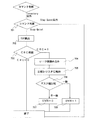
次に、図1におけるICチップでのアンチコリジョン機能のプログラムの動作を、図4のフローチャートと対応させながら説明する。 Next, the operation of the anti-collision function program in the IC chip in FIG. 1 will be described with reference to the flowchart of FIG.
まず、ICチップが有するリセット回路110は、受信信号120を受けて演算回路106にリセットをかける(初期リセット:ステップ401)。復調回路112はリセットがかかると受信信号120の復調を開始し、コード抽出回路118へ復調された受信データ122を出力する。コード抽出回路118は復調された受信データ122から制御コードを抽出し制御レジスタ117へ書き込む。
First, the reset circuit 110 included in the IC chip receives the reception signal 120 and resets the arithmetic circuit 106 (initial reset: step 401). When reset, the demodulation circuit 112 starts demodulating the reception signal 120 and outputs the
ICチップが有するCPU102は、制御レジスタ117にコード抽出回路からの信号の書き込みがあると動作を開始する(開始:ステップ402)。CPU102は、制御レジスタ117内の制御コードにSOF(Start Of Frame)が含まれていれば(制御レジスタ判断:ステップ403)、ROM103からアンチコリジョンプログラムを読み込み(プログラム読み込み:ステップ404)、アンチコリジョンプログラム内のアンチコリジョンルーチンを実行する(ルーチン実行:ステップ409)。一方、制御レジスタ117の制御コードにSOFが含まれていなければ初期リセット後のステップ401の状態に戻る。なお、CPU102は、アンチコリジョンルーチンの実行終了後、初期リセット後のステップ401の状態に戻る。
The
なお、本発明においてアンチコリジョンプログラムを実行させるためのCPU102のクロック周波数は、1MHz以上とすることが好ましく、より好ましくは100MHz以上とするが好ましい。なお、CPUにおける処理を複数のCPUで分割し、パイプライン処理を行うことで、より低いクロック周波数のCPUであってもアンチコリジョンプログラムを高速で実行させることができるため好適である。
In the present invention, the clock frequency of the
次に、図1におけるICチップでのアンチコリジョン機能を実現するためのアンチコリジョンプログラム内のアンチコリジョンルーチンを図5〜9を用いて説明する。 Next, an anti-collision routine in the anti-collision program for realizing the anti-collision function in the IC chip in FIG. 1 will be described with reference to FIGS.
まず、図5に示すフローチャートと対応させながらアンチコリジョンルーチンの動作を説明する。CPU102は、ROM103からアンチコリジョンプログラムを読み込み、アンチコリジョンルーチンを開始する(ルーチン開始:ステップ501)。CPU102は、制御レジスタ117のフラグコードを読み込み、RAM104へ書き込む(フラグ取得:ステップ502)。次に、CPU102は、制御レジスタ117のコマンドコードを読み込み、RAM104へ書き込む(コマンド取得:ステップ503)。CPU102は、コマンドコードの種類によって処理をInventoryとInventory以外に分岐(コマンド判断ルーチン:ステップ509)させ(図5の(A)、(B)、(C)、(D))、さらに複数のルーチンを実行させることができる。最後に、CPU102はアンチコリジョンするための複数のルーチンを終了する(終了:ステップ504)。
First, the operation of the anti-collision routine will be described with reference to the flowchart shown in FIG. The
次に図6のフローチャートと対応させながら図1におけるICチップでのコマンドコード別処理の詳細を説明する。 Next, the details of the process for each command code in the IC chip in FIG. 1 will be described with reference to the flowchart of FIG.
図6にInventoryコマンドのフローチャートを示す(図5における(A))。CPU102は、制御レジスタ117のマスク値コードを読み込み、RAM104へ書き込む(マスク値取得:ステップ601)。CPU102は、制御レジスタ117のマスク長コードを読み込み、RAM104へ書き込む(マスク長取得:ステップ602)。CPU102は、マスク長コードの値によって処理を分岐させる(マスク長判断:ステップ603)。マスク長コードの値が0以外のときのみ、CPU102は、UID値を読み込み(UID値読み込み:ステップ604)、マスク長コード分だけ右シフト(UID値を右シフト:ステップ605)させ、最下位ビットよりlogN/log2ビット分(本実施の形態では4ビット分)をスロットレジスタに格納(スロットレジスタに格納:ステップ606)する。
FIG. 6 shows a flowchart of the Inventory command ((A) in FIG. 5). The
次に図7にマスク長判断のフローチャートを示す(図5における(B))。CPU102は、マスク長コードの値によって処理を分岐(マスク長判断ルーチン:ステップ611)させる。CPU102は、マスク長コードが0の時に、OUTJUDGEフラグを1にする(OUTJUDGE=1:ステップ619)。一方、CPU102は、マスク長コードが0以外の時には、CRCフラグの値によって処理を分岐させる(CRC判断:ステップ612)。CPU102は、CRCフラグが0の時に、OUTJUDGEフラグを0にする(OUTJUDGE≠1:ステップ618)。CPU102は、CRCフラグが1の時には、STATEフラグの値によって処理を分岐させる(STATE判断:ステップ613)。CPU102は、STATEフラグが0以外の時に、OUTJUDGEフラグを0にする(OUTJUDGE≠1:ステップ618)。CPU102は、STATEフラグが0の時に、UID値を読み込み(UID値読み込み:ステップ614)、最下位ビットよりマスク長コードビット分だけ、比較レジスタに格納する(UID値の最下位ビットよりマスク長分を比較レジスタに格納;ステップ615)。最後にCPU102は、マスク値コードを読み込み(マスク値読み込み:ステップ616)、最下位ビットよりマスク長コード分を比較レジスタと比較し(比較レジスタ=マスク値:ステップ617)、一致したときはOUTJUDGEフラグを1にする(OUTJUDGE=1:ステップ619)。一方、一致しなかったときは、OUTJUDGEフラグを0にする(OUTJUDGE≠1:ステップ618)。
Next, FIG. 7 shows a flowchart for determining the mask length ((B) in FIG. 5). The
なおCRCフラグは、受信信号のCRC305と、CPU102がデータ304から演算したCRCとが一致した場合にはCRCフラグ「1」、一致しない場合にはCRCフラグ「0」の情報を有する。
The CRC flag has information of CRC flag “1” when the
またOUTJUDGEフラグは、ICチップよりリーダライタに応答動作を行うか否かを規定する信号である。応答動作を行うためにUID値を制御レジスタ117に書き込む場合には「OUTJUDGE=1」、それ以外の状態では、「OUTJUDGE=0」との情報を有する。
The OUTJUDGE flag is a signal that defines whether or not a response operation is performed from the IC chip to the reader / writer. When the UID value is written to the
またSTATEフラグは、ICチップよりリーダライタへの応答動作を行うか否かを、上述のOUTJUDGEフラグが「1」または「0」に関わらず規定する信号である。ICチップよりリーダライタへの応答動作を行う場合には「STATE=0」、それ以外の状態では、「STATE≠0」(STATE=1を含む)との情報を有する。 The STATE flag is a signal that defines whether or not a response operation from the IC chip to the reader / writer is performed regardless of whether the above-described OUTJUDGE flag is “1” or “0”. When the response operation from the IC chip to the reader / writer is performed, the information includes “STATE = 0”, and in other states, “STATE ≠ 0” (including STATE = 1).
CRCフラグ、OUTJUDGEフラグ、STATEフラグ等のフラグコードは、RAM104の送信データレジスタ203、受信データレジスタ204、比較レジスタ205、スロットレジスタ206に用いる以外の領域を用いて、処理が行われる。
The flag codes such as the CRC flag, OUTJUDGE flag, and STATE flag are processed using areas other than those used for the transmission data register 203, the reception data register 204, the comparison register 205, and the slot register 206 in the
CPU102は、フラグコードを読み込み、フラグコードの種類によって処理をNスロット(本実施の形態ではN=16)と1スロットに分岐させ、いずれかの処理を実行する。
The
次に図8にスロット判断(N/1スロット判断:ステップ621)のフローチャートを示す(図5における(C))。CPU102は、1スロットの処理を開始すると、制御レジスタ117の状態がEOFであることを検出するまで待ち(EOF検出:ステップ622)、その後、OUTJUDGEフラグ(OUTJUDGE判断;ステップ623)が1であれば、UID値を制御レジスタ117へ書き込み(UID応答:ステップ624)、応答動作を開始させ、アンチコリジョンルーチンを終了する。CPU102は、16スロットの処理を開始すると、スロットカウンタへ0を代入する(SLOT=0:ステップ625)。次にCPU102は、制御レジスタ117の状態がEOFであることを検出するまで待ち(EOF検出:ステップ626)、その後、OUTJUDGEフラグが1(OUTJUDGE判断;ステップ627)で且つスロットカウンタ値がスロットレジスタ値と同じである(スロット値比較;ステップ628)ときのみ、UID値を制御レジスタ117へ書き込み(UID応答:ステップ629)、応答動作を開始させる。CPU102は、スロットカウンタ値を1増加させる(SLOT=SLOT+1:ステップ630)。CPU102は、スロットカウンタ値が16のときにアンチコリジョンルーチンを終了させ、スロットカウンタ値が16より小さいとき(SLOT判断:ステップ631)には、再び、制御レジスタ117の状態がEOFであることを検出するまで待つ(EOF検出:ステップ626)。
Next, FIG. 8 shows a flowchart of slot determination (N / 1 slot determination: step 621) ((C) in FIG. 5). When the
なお、SLOTの演算は、RAM104の送信データレジスタ203、受信データレジスタ204、比較レジスタ205、スロットレジスタ206に用いる以外の領域を用いて、処理が行われる。
The SLOT calculation is performed using areas other than those used for the transmission data register 203, the reception data register 204, the comparison register 205, and the slot register 206 of the
図9にInventory以外のコマンドのフローチャートを示す(図5における(D))。CPU102は、コマンドコードの種類によって処理をStayQuietとStayQuiet以外に分岐させ(コマンド判断:ステップ701)、いずれかのルーチンを実行させることができる。
FIG. 9 shows a flowchart of commands other than Inventory ((D) in FIG. 5). The
図9のフローチャートについて説明する。CPU102は、StayQuietコマンドの処理を開始すると、制御レジスタ117の状態がEOFであることを検出するまで待つ(EOF検出:ステップ702)。CPU102は、CRCフラグが0の時に、STATEフラグを変更せずに、アンチコリジョンルーチンを終了する。一方、CPU102は、CRCフラグが1の時に、UID値を読み込み(UID値読み込み:ステップ704)、比較レジスタに格納する(比較レジスタに格納:ステップ705)。CPU102は、マスク値コードを読み込み、比較レジスタと比較し(マスク値比較:ステップ706)、一致しなかったときはSTATEフラグを0にして(STATE=0:ステップ707)、アンチコリジョンルーチンを終了する。一致したときは、STATEフラグを1にして(STATE=1:ステップ708)、アンチコリジョンルーチンを終了する。また、CPU102は、StayQuietコマンド以外の処理はアンチコリジョンルーチンを終了する。
The flowchart of FIG. 9 will be described. When the
以上のような形態とすることで、アンチコリジョン機能を有するICチップにおいて、製品毎の無線手段の信号の種類や、規格が変更になることに伴う仕様の変更により、ICチップのマスク設計の段階から作り直す必要ない。そのため、アンチコリジョンプログラムの変更だけで対応することができ、製造コストの削減及び製造時間の短縮ができる。また、マスク設計の変更によって再度作り直したICチップが不具合といった懸念もない。 In the IC chip having the anti-collision function, the mask design stage of the IC chip can be realized by changing the type of the wireless means signal for each product or the specification change due to the change of the standard. There is no need to recreate from. Therefore, it can be dealt with only by changing the anti-collision program, and the manufacturing cost and the manufacturing time can be reduced. Further, there is no concern that the IC chip remade by changing the mask design is defective.
また従来においては、専用の衝突防止機能を有するICチップを製造する際においては、衝突防止機能を備えた回路を搭載することもあった。しかしながら、本発明では衝突防止機能を読み出し専用メモリにプログラムとして格納するため、衝突防止機能を備えた回路よりも読み出し専用メモリの方が作りやすいといった利点が得られるため、ICチップの不具合の削減を図ることができる。 Conventionally, when an IC chip having a dedicated collision prevention function is manufactured, a circuit having a collision prevention function is sometimes mounted. However, in the present invention, since the collision prevention function is stored as a program in the read-only memory, the advantage that the read-only memory is easier to make than the circuit having the collision prevention function can be obtained. You can plan.
なお、本実施の形態は、本明細書中の他の実施の形態のいかなる記載とも自由に組み合わせて実施することが可能である。
(実施の形態2)
Note that this embodiment mode can be freely combined with any description in other embodiment modes in this specification.
(Embodiment 2)
実施の形態1においては、アンチコリジョン機能を行うための複数のルーチンを有するアンチコリジョンプログラムをROMに格納することによりにICチップがアンチコリジョン機能を取りうる構成について示した。本実施の形態においては、実施の形態1とは異なる形態のアンチコリジョン機能を実現するための装置構成及び、回路構成について説明する。フローチャートについては実施の形態と同様であるため、必要に応じて実施の形態で述べた図を用いて説明する。 In the first embodiment, the configuration in which the IC chip can take the anti-collision function by storing the anti-collision program having a plurality of routines for performing the anti-collision function in the ROM has been described. In this embodiment, a device configuration and a circuit configuration for realizing an anti-collision function having a different form from that of the first embodiment will be described. Since the flowchart is the same as that of the embodiment, description will be made using the drawings described in the embodiment as necessary.
図10に本発明におけるアンチコリジョン機能を搭載する対象であるICチップのブロック図を示す。図10は実施の形態1における図1のICチップのブロック図に補助演算回路1001を加えたものであり、図1と同様にCPU102と、ROM103と、RAM104と、コントローラ105と、からなる演算回路106と、アンテナ107と、共振回路108と、電源回路109と、リセット回路110と、クロック生成回路111と、復調回路112と、変調回路113と、電源管理回路114と、からなるアナログ部115と、を有する。コントローラ105は、CPUインターフェース(CPUIF)116と、制御レジスタ117と、コード抽出回路118と、符号化回路119と、から構成される。
FIG. 10 shows a block diagram of an IC chip which is a target for mounting the anti-collision function in the present invention. FIG. 10 is a block diagram of the IC chip of FIG. 1 according to
このようなICチップにおけるアンチコリジョン機能の処理は、実施の形態1と同じであるが、一部処理を補助演算回路1001で行う。
The processing of the anti-collision function in such an IC chip is the same as that of the first embodiment, but a part of the processing is performed by the auxiliary
この補助演算回路1001に搭載する回路として好適なものは、シフト演算回路、CRC演算回路、がある。具体的には、図6におけるUID値を右シフト(ステップ605)には右シフト回路が、図7、図9におけるCRC判断(ステップ612、ステップ703)にはCRC演算回路が適している。
Suitable circuits mounted on the auxiliary
次に、シフト演算回路の一例である4ビットパラレル入力−パラレル出力、右シフト回路の回路構成を図11に示す。右シフト回路は、2入力セレクタとOR回路で構成される。右シフト回路は、入力信号をシフト信号値分だけ右シフトさせて、出力信号として出力する。本回路構成は、右シフト、ビット幅4ビットに限定されること無く、左シフトやより広いビット幅入力を持つ回路にも適用可能である。 Next, FIG. 11 shows a circuit configuration of a 4-bit parallel input-parallel output, right shift circuit which is an example of a shift operation circuit. The right shift circuit includes a 2-input selector and an OR circuit. The right shift circuit shifts the input signal to the right by the shift signal value and outputs it as an output signal. This circuit configuration is not limited to a right shift and a bit width of 4 bits, but can also be applied to a circuit having a left shift and a wider bit width input.
図11において、第1の入力信号822と、第2の入力信号823と、第3の入力信号824と、第4の入力信号825と、からなる4ビット入力信号は、セレクタ805〜814へ入力される。第1のシフト信号820と、第2のシフト信号821と、からなる2ビットシフト信号は、OR回路801〜804へ入力され、セレクタ選択信号となって、セレクタ805〜814を制御する。
In FIG. 11, a 4-bit input signal including a first input signal 822, a second input signal 823, a third input signal 824, and a fourth input signal 825 is input to
本実施形態の一例である4ビットパラレル入力−パラレル出力の動作を以下に説明する。なお、入力信号は2進数で「1111」、シフト信号は2進数で「01」であるときの動作を説明する。 An operation of 4-bit parallel input-parallel output, which is an example of this embodiment, will be described below. The operation when the input signal is “1111” in binary and the shift signal is “01” in binary will be described.
シフト信号が「01」であるとき、OR回路803のみ「1」を出力し、その他OR回路はすべて「0」を出力する。OR回路803の出力した「1」を受け取ったセレクタ807、810、812は、それぞれ第2の入力信号823である「1」、第3の入力信号824である「1」、第4の入力信号825である「1」を、セレクタ808、811、812へ出力する。OR回路804の出力した「0」によって動作するセレクタ808、811、813、814は、それぞれ、セレクタ807の出力した値である「1」、セレクタ810の出力した値である「1」、セレクタ812の出力した値である「1」、あらかじめセットされた「0」を第1の出力信号826、第2の出力信号827、第3の出力信号828、第4の出力信号829へ出力する。
When the shift signal is “01”, only the OR circuit 803 outputs “1”, and all other OR circuits output “0”. The selectors 807, 810, and 812 that have received “1” output from the OR circuit 803 are “1” that is the second input signal 823, “1” that is the third input signal 824, and the fourth input signal, respectively. “1” that is 825 is output to the
したがって、出力信号は2進数で「0111」となり、入力信号「1111」を右へ1ビットシフトした値となる。 Therefore, the output signal is “0111” in binary, and is a value obtained by shifting the input signal “1111” by 1 bit to the right.
次に、CRC演算回路の一例であるCRC−16受信回路の構成を図12に示す。CRC−16受信回路は、シフトレジスタとXOR回路で構成された巡回型シフトレジスタ回路である。CRC−16受信回路は、入力信号をCRC生成多項式(X16+X12+X5+1)で除算する。除算した結果、余りが無ければ入力信号が正しいものであることがわかり、余りがあれば入力信号が間違っていることがわかる。本回路構成は、CRC−16受信回路に限定されること無く、CRC−CCIT、CRC−12、CRC−32回路にも適用可能である。 Next, FIG. 12 shows a configuration of a CRC-16 receiving circuit which is an example of a CRC arithmetic circuit. The CRC-16 receiving circuit is a cyclic shift register circuit composed of a shift register and an XOR circuit. The CRC-16 receiving circuit divides the input signal by the CRC generator polynomial (X 16 + X 12 + X 5 +1). As a result of division, if there is no remainder, it can be seen that the input signal is correct, and if there is a remainder, it can be seen that the input signal is wrong. This circuit configuration is not limited to the CRC-16 receiving circuit, but can also be applied to CRC-CCIT, CRC-12, and CRC-32 circuits.
本実施形態の一例であるCRC−16受信回路の動作を以下に説明する。 The operation of the CRC-16 receiving circuit as an example of this embodiment will be described below.
シフトレジスタ903、905、907は、リセット信号911を受けて、レジスタを「0」にセットする。動作クロック910のタイミングで任意のビット数を持つ入力信号901の最初のビットがXOR回路908に入力されると、その値は、4ビットシフトレジスタ903より出力された「0」とXOR演算され、5ビットシフトレジスタ907へ入力される。その後、4クロック後に最初のビットは、XOR回路906で、4ビットシフトレジスタ903より出力された「0」と再びXOR演算され、7ビットシフトレジスタ905へ入力される。このような処理を繰り返し、最初のビットは、XOR回路904、4ビットシフトレジスタ903を経て、出力信号902として出力される。
The shift registers 903, 905, and 907 receive the reset signal 911 and set the registers to “0”. When the first bit of the
なお、上記処理は、任意のビット数を持つ入力信号901をCRC−16生成多項式(X16+X12+X5+1)で除算を行ったことと同じことである。
The above processing is the same as dividing the
これら機能を有する回路を補助演算回路1001に含み、CPU102の命令によって動作することで、ROM103に搭載されたルーチンよりも高速に処理を行うことが可能になる。
By including a circuit having these functions in the auxiliary
以上のような形態とすることで、アンチコリジョン機能を有するICチップにおいて、製品毎の無線手段の信号の種類や、規格が変更になることに伴う仕様の変更により、ICチップのマスク設計の段階から作り直す必要ない。そのため、アンチコリジョンプログラムの変更だけで対応することができ、製造コストの削減及び製造時間の短縮ができる。また、マスク設計の変更によって再度作り直したICチップが不具合といった懸念もない。 In the IC chip having the anti-collision function, the mask design stage of the IC chip can be realized by changing the type of the wireless means signal for each product or the specification change due to the change of the standard. There is no need to recreate from. Therefore, it can be dealt with only by changing the anti-collision program, and the manufacturing cost and the manufacturing time can be reduced. Further, there is no concern that the IC chip remade by changing the mask design is defective.
また従来においては、専用の衝突防止機能を有するICチップを製造する際においては、衝突防止機能を備えた回路を搭載することもあった。しかしながら、本発明では衝突防止機能を読み出し専用メモリにプログラムとして格納するため、衝突防止機能を備えた回路よりも読み出し専用メモリの方が作りやすいといった利点が得られるため、ICチップの不具合の削減を図ることができる。 Conventionally, when an IC chip having a dedicated collision prevention function is manufactured, a circuit having a collision prevention function is sometimes mounted. However, in the present invention, since the collision prevention function is stored as a program in the read-only memory, the advantage that the read-only memory is easier to make than the circuit having the collision prevention function can be obtained. Can be planned.
なお、本実施の形態は、本明細書中の他の実施の形態のいかなる記載とも自由に組み合わせて実施することが可能である。
(実施の形態3)
Note that this embodiment mode can be freely combined with any description in other embodiment modes in this specification.
(Embodiment 3)
本実施の形態では、絶縁基板上に形成された薄膜トランジスタによりICチップを形成する形態について説明する。 In this embodiment mode, a mode in which an IC chip is formed using a thin film transistor formed over an insulating substrate will be described.
図13(A)に示すように、絶縁基板1300を用意する。絶縁基板1300には、ガラス基板、石英基板、プラスチック基板等が挙げられる。また、これら基板において、その裏面を研磨する等の手法によって薄くすることができる。さらに、金属元素等の導電性基板や、シリコン等の半導体性基板上に絶縁性を有する材料を用いて層を形成した基板を用いることも可能である。ICチップを、例えばプラスチック基板に形成することにより、柔軟性が高く、軽量で薄型な装置を作製することができる。
As shown in FIG. 13A, an insulating
絶縁基板1300上に剥離層1301を選択的に形成する。勿論、剥離層1301を絶縁基板1300全面に形成しても良い。剥離層1301はスパッタリング法やプラズマCVD法等により、タングステン(W)、モリブデン(Mo)、チタン(Ti)、タンタル(Ta)、ニオブ(Nb)、ニッケル(Ni)、コバルト(Co)、ジルコニウム(Zr)、亜鉛(Zn)、ルテニウム(Ru)、ロジウム(Rh)、パラジウム(Pd)、オスミウム(Os)、イリジウム(Ir)、珪素(Si)から選択された元素、又は前記元素を主成分とする合金材料、又は前記元素を主成分とする化合物材料からなる層を、単層又は積層して形成する。珪素を含む層の結晶構造は、非晶質、微結晶、多結晶のいずれの場合でもよい。
A
剥離層1301上に下地層1302を形成する。下地層1302は、酸化珪素、窒化珪素、または酸化窒化珪素等の絶縁性を有する材料を用い、単層構造または積層構造で形成することができる。積層構造を用いる場合、下地層1302の一層目として、膜厚10nm以上200nm以下(好ましくは50nm以上100nm以下)の酸化窒化珪素層を形成する。当該酸化窒化珪素層は、プラズマCVD法を用い、SiH4、NH3、N2O及びH2を反応ガスとして形成することができる。次いで下地層1302のニ層目として、膜厚50nm以上200nm以下(好ましくは100nm以上150nm以下)の酸化窒化珪素層を形成する。当該酸化窒化珪素層は、プラズマCVD法を用い、SiH4及びN2Oを反応ガスとして形成することができる。
A
下地層1302上に半導体層1304を形成する。半導体層1304は、シリコン材料、又はシリコンとゲルマニウムからなる材料等、シリコン半導体層を用いて形成することができる。半導体層1304の結晶構造は非晶質、微結晶、多結晶のいずれでもよい。
A
多結晶の半導体層を形成するには、非晶質半導体層に対して加熱処理を行う手法がある。加熱処理には、レーザ照射、加熱炉、ランプ照射等が挙げられ、これらのいずれか一又は複数を用いることができる。 In order to form a polycrystalline semiconductor layer, there is a method of performing heat treatment on the amorphous semiconductor layer. Examples of the heat treatment include laser irradiation, a heating furnace, lamp irradiation, and the like, and any one or more of them can be used.
レーザ照射には、連続発振型のレーザビーム(CWレーザ)やパルス発振型のレーザビーム(パルスレーザ)を用いることができる。レーザビームとしては、Arレーザ、Krレーザ、エキシマレーザ、YAGレーザ、Y2O3レーザ、YVO4レーザ、YLFレーザ、YAlO3レーザ、ガラスレーザ、ルビーレーザ、アレキサンドライトレーザ、Ti:サファイヤレーザ、銅蒸気レーザまたは金蒸気レーザのうち一種または複数種から発振されるものを用いることができる。このようなレーザビームの基本波と、当該基本波の第2高調波から第4高調波といった高調波のレーザビームのいずれかを照射することで、粒径の大きな結晶を有するシリコン層を得ることができる。高調波には、Nd:YVO4レーザ(基本波1064nm)の第2高調波(532nm)や第3高調波(355nm)を用いることができる。レーザ照射におけるエネルギー密度は0.01〜100MW/cm2程度(好ましくは0.1〜10MW/cm2)が必要である。そして、走査速度を10〜2000cm/sec程度として照射する。 For laser irradiation, a continuous wave laser beam (CW laser) or a pulsed laser beam (pulse laser) can be used. As the laser beam, Ar laser, Kr laser, excimer laser, YAG laser, Y 2 O 3 laser, YVO 4 laser, YLF laser, YAlO 3 laser, glass laser, ruby laser, alexandrite laser, Ti: sapphire laser, copper vapor A laser or a gold vapor laser oscillated from one or a plurality of types can be used. By irradiating either a fundamental wave of such a laser beam or a harmonic laser beam such as the second harmonic to the fourth harmonic of the fundamental wave, a silicon layer having a crystal with a large grain size is obtained. Can do. As the harmonic, the second harmonic (532 nm) or the third harmonic (355 nm) of an Nd: YVO 4 laser (fundamental wave 1064 nm) can be used. Energy density of laser irradiation of about 0.01 to 100 MW / cm 2 (preferably 0.1 to 10 MW / cm 2) is required. Then, irradiation is performed at a scanning speed of about 10 to 2000 cm / sec.
なお、基本波のCWレーザと高調波のCWレーザとを照射するようにしてもよいし、基本波のCWレーザと高調波のパルスレーザとを照射するようにしてもよい。複数のレーザ光を照射することにより、広範囲のエネルギー領域を補うことができる。 The fundamental CW laser and the harmonic CW laser may be irradiated, or the fundamental CW laser and the harmonic pulse laser may be irradiated. By irradiating a plurality of laser beams, a wide energy range can be compensated.
また、パルスレーザであって、非晶質状態を有するシリコン層がレーザによって溶融してから固化するまでに、次のパルスのレーザを照射できるような発振周波数でレーザを発振させるレーザビームを用いることもできる。このような周波数でレーザを発振させることで、走査方向に向かって連続的に成長した結晶粒を有するシリコン層を得ることができる。このようなレーザの発振周波数は10MHz以上であり、通常用いられている数十Hz〜数百Hzの周波数帯よりも著しく高い。 In addition, a pulse laser that uses a laser beam that oscillates at an oscillation frequency capable of irradiating a laser of the next pulse before the amorphous silicon layer is melted by the laser and solidified is used. You can also. By oscillating the laser at such a frequency, a silicon layer having crystal grains continuously grown in the scanning direction can be obtained. The oscillation frequency of such a laser is 10 MHz or more, which is significantly higher than a frequency band of several tens to several hundreds Hz that is normally used.
加熱処理として加熱炉を用いる場合には、非晶質状態を有する半導体層を400〜550℃で2〜20時間かけて加熱する。このとき、徐々に高温となるように温度を400〜550℃の範囲で多段階に設定するとよい。最初の400℃程度の低温加熱工程により、非晶質状態を有する半導体層に含まれる水素等が出てくるため、結晶化の際に層表面が荒れるのを低減することができる。 In the case of using a heating furnace as the heat treatment, the semiconductor layer having an amorphous state is heated at 400 to 550 ° C. for 2 to 20 hours. At this time, the temperature may be set in multiple stages in the range of 400 to 550 ° C. so that the temperature gradually increases. In the first low-temperature heating process at about 400 ° C., hydrogen and the like contained in the semiconductor layer having an amorphous state are produced, so that the layer surface can be prevented from being roughened during crystallization.
上記加熱処理の行程において、半導体層の結晶化を促進させる金属、例えばニッケル(Ni)を添加する。例えば、非晶質状態を有する珪素層上にニッケルを含む溶液を塗布し、加熱処理を行うことができる。このように金属を用いて加熱処理を行うことで、加熱温度を低減することができ、さらに、結晶粒界の連続した多結晶珪素層を得ることができる。ここで結晶化を促進するための金属としてはNiの他に、鉄(Fe)、ルテニウム(Ru)、ロジウム(Rh)、パラジウム(Pd)、オスミウム(Os)、イリジウム(Ir)、白金(Pt)、銅(Cu)、銀(Au)等を用いることもできる。 In the heat treatment process, a metal that promotes crystallization of the semiconductor layer, for example, nickel (Ni) is added. For example, a solution containing nickel can be applied to a silicon layer having an amorphous state, and heat treatment can be performed. By performing heat treatment using a metal in this manner, the heating temperature can be reduced, and a polycrystalline silicon layer having continuous crystal grain boundaries can be obtained. Here, as a metal for promoting crystallization, in addition to Ni, iron (Fe), ruthenium (Ru), rhodium (Rh), palladium (Pd), osmium (Os), iridium (Ir), platinum (Pt ), Copper (Cu), silver (Au), or the like can also be used.
結晶化を促進させる金属はメモリセル等の汚染源となるため、半導体層を結晶化した後に、金属を除去するゲッタリング行程を行うことが望ましい。ゲッタリング行程では、半導体層を結晶化した後、半導体層上にゲッタリングシンクとなる層を形成し、加熱することで金属をゲッタリングシンクへ移動させる。ゲッタリングシンクには、多結晶半導体層や不純物が添加された半導体層を用いることができる。例えば、多結晶珪素層上にアルゴン等の不活性元素が添加された多結晶半導体層を形成し、これをゲッタリングシンクとして用いることができる。ゲッタリングシンクに不活性元素を添加することによって、ひずみを生じさせ、より効率的に金属を捕獲することができる。また新たにゲッタリングシンクを形成することなく、TFTの半導体層の一部にリン等の元素を添加することによって、金属を捕獲することもできる。 Since the metal that promotes crystallization serves as a contamination source for memory cells and the like, it is desirable to perform a gettering step for removing the metal after crystallization of the semiconductor layer. In the gettering step, after the semiconductor layer is crystallized, a layer serving as a gettering sink is formed on the semiconductor layer, and the metal is moved to the gettering sink by heating. As the gettering sink, a polycrystalline semiconductor layer or a semiconductor layer to which an impurity is added can be used. For example, a polycrystalline semiconductor layer to which an inert element such as argon is added can be formed on the polycrystalline silicon layer, and this can be used as a gettering sink. By adding an inert element to the gettering sink, distortion can be generated and the metal can be captured more efficiently. In addition, a metal can be captured by adding an element such as phosphorus to a part of the semiconductor layer of the TFT without forming a new gettering sink.
このように形成された半導体層を、所定の形状に加工し、島状の半導体層1304を形成する。加工手段には、フォトリソグラフィ法によって形成されたマスクを用いて、エッチングする。エッチングには、ウェットエッチング法又はドライエッチング法を適用することができる。
The semiconductor layer thus formed is processed into a predetermined shape, so that an island-shaped
半導体層1304を覆うようにゲート絶縁層1305として機能する絶縁層を形成する。ゲート絶縁層1305は、下地層1302と同様の材料、方法により形成することができる。
An insulating layer functioning as the
図13(B)に示すように、ゲート絶縁層1305を介してゲート電極層1306として機能する導電層を形成する。ゲート電極層1306はアルミニウム(Al)、チタン(Ti)、モリブデン(Mo)、タンタル(Ta)、タングステン(W)もしくはシリコン(Si)の元素からなる膜又はこれらの元素を有する合金膜を用いることができる。ゲート電極層1306は、単層構造又は積層構造とすることができ、積層構造として窒化タンタルとタングステンの積層構造を適用することができる。ゲート電極層1306の加工手段には、フォトリソグラフィ法によって形成されたマスクを用いて、エッチングする。エッチングには、ウェットエッチング法又はドライエッチング法を適用することができる。
As shown in FIG. 13B, a conductive layer functioning as the
ゲート電極層1306の側面にサイドウォール1307と呼ばれる絶縁物を形成する。サイドウォール1307は、下地層1302と同様の材料、方法により形成することができる。またサイドウォール1307の端部にテーパ形状を有するためには、等方性エッチングを用いればよい。サイドウォール1307により、ゲート長が狭くなるにつれて生じる短チャネル効果を防止することができる。短チャネル効果はNチャネル型TFTに顕著であるため、少なくともNチャネル型TFTのゲート電極側面に設けるとよい。
An insulator called a
このような状態で、ゲート絶縁層1305をエッチングする。その結果、半導体層1304の一部や下地層1302が露出する。エッチングには、ウェットエッチング法又はドライエッチング法を適用することができる。
In such a state, the
そして、ゲート電極層1306、及びサイドウォール1307を用いて、半導体層1304に不純物元素を添加し、高濃度不純物領域1310、1312を形成する。Nチャネル型TFTとする場合、不純物元素はリン(P)を用い、Pチャネル型TFTとする場合、不純物元素はボロン(B)を用いることができる。このとき、不純物元素の添加量によっては、サイドウォール1307下方に低濃度不純物領域が形成される。本実施の形態ではNチャネル型の不純物領域にのみ低濃度不純物領域1311を形成する。低濃度不純物領域1311は、短チャネル効果を防止することができるからである。このような低濃度不純物領域を有する構造をLDD(Lightly Doped Drain)構造と呼ぶ。
Then, an impurity element is added to the
その後、下地層1302、半導体層1304、ゲート電極層1306、サイドウォール1307を覆うように絶縁層1314を形成する。絶縁層1314は、CVD法によってシリコンを有する材料から形成するとよい。
After that, an insulating
絶縁層1314を形成後、必要に応じて加熱処理を行う。加熱処理には、上記結晶化と同様な手段を用いることができる。加熱処理により、不純物領域の活性化を行うことができる。CVD法により形成された絶縁層1314は、水素を多く含むため、上記加熱処理により水素が拡散し、不純物領域の膜あれを低減することができる。
After the insulating
図13(C)に示すように、層間膜として機能する絶縁層1315、1316を形成する。絶縁層1315、1316には、無機材料又は有機材料を用いることができる。無機材料は、酸化珪素、窒化珪素、酸化窒化珪素等を用いることができる。有機材料はポリイミド、アクリル、ポリアミド、ポリイミドアミド、レジスト又はベンゾシクロブテン、シロキサン、ポリシラザンを用いることができる。なお、シロキサンとは、シリコン(Si)と酸素(O)との結合で骨格構造が構成される。置換基として、少なくとも水素を含む有機基(例えばアルキル基、芳香族炭化水素)が用いられる。置換基として、フルオロ基を用いてもよい。または置換基として、少なくとも水素を含む有機基と、フルオロ基とを用いてもよい。ポリシラザンは、シリコン(Si)と窒素(N)の結合を有するポリマー材料を出発原料として形成される。無機材料を用いると不純物元素の侵入を防止することができ、有機材料を用いると平坦性を高めることができる。そのため、本実施の形態では、絶縁層1315に無機材料を用い、絶縁層1316に有機材料を用いる。
As shown in FIG. 13C, insulating
絶縁層1314、1315、1316にコンタクトホールを形成して配線1318を形成する。配線1318は、アルミニウム(Al)、チタン(Ti)、モリブデン(Mo)、タンタル(Ta)、タングステン(W)もしくはシリコン(Si)の元素からなる膜又はこれらの元素を有する合金膜を用いることができる。配線1318は、単層構造又は積層構造を用いることができ、例えば第1層にタングステン、窒化タングステン等を用い、第2層にアルミニウムとシリコンの合金(Al−Si)、アルミニウムとチタンの合金(Al−Ti)を用い、第3層に窒化チタン膜、チタン膜等を順次積層した構造を適用することができる。配線1318の加工には、フォトリソグラフィ法で形成されたマスクを用いた、エッチング法がある。エッチング法には、ウェットエッチング法又はドライエッチング法を適用することができる。配線1318は、半導体層1304では不純物領域に接続し、このような配線をソース電極、ドレイン電極と呼ぶことができる。
Contact holes are formed in the insulating
このようにして、Nチャネル型TFT1330、Pチャネル型TFT1331を形成することができる。
In this manner, an N-
その後必要に応じて、配線1318上に保護膜1319を形成する。保護膜1319は、珪素を有する酸化物、又は珪素を有する窒化物によって形成することができる。例えば、窒化珪素を用いて保護膜1319を形成する。その結果、水分や酸素の侵入を防止することができる。
Thereafter, a
図13(D)に示すように、TFT間に開口部を形成し、エッチング剤1325を導入する。開口部はウェットエッチング法又はドライエッチング法を用いて形成することができる。なお開口部の形成位置は、TFT間でなくともよく、半導体層1304が形成されない領域であればよい。エッチング剤1325は、ウェットエッチング法であれば、フッ酸を水やフッ化アンモニウムで希釈した混液、フッ酸と硝酸の混液、フッ酸と硝酸と酢酸の混液、過酸化水素と硫酸の混液、過酸化水素とアンモニウム水と水の混液、過酸化水素と塩酸と水の混液等を用いる。また、ドライエッチング法であれば、フッ素等のハロゲン系の原子や分子を含む気体、又は酸素を含む気体を用いる。好ましくは、エッチング剤として、フッ化ハロゲン又はハロゲン間化合物を含む気体又は液体、例えば三フッ化塩素(ClF3)を適用することができる。
As shown in FIG. 13D, an opening is formed between the TFTs, and an
エッチング剤を導入することにより、剥離層1301が除去される。すると、絶縁基板1300が剥離される。このようにして、薄型化、軽量化を達成したICチップを形成することができる。
By introducing the etching agent, the
エッチング剤を導入する方法以外に、レーザ描画により剥離層1301を露出させたり、ICチップの側面に切り込みをいれる等して、物理的に絶縁基板1300を剥離させてもよい。
In addition to the method of introducing an etchant, the insulating
図13(E)に示すように、フィルム1327、1328によって覆い、ICチップを完成させることができる。このとき、接着層1329を用いて、フィルム1327や1328と貼り合わせてもよい。フィルム1327、1328には、水分や酸素等の侵入を防ぐために、保護膜を形成しても良い。また配線1318上には保護膜1319が形成されているため、下地層1302又は接着層1329の下方に保護膜を形成してもよい。保護膜は、珪素を有する酸化物、又は珪素を有する窒化物によって形成することができる。
As shown in FIG. 13E, an IC chip can be completed by covering with
このように絶縁基板上、さらに絶縁基板を剥離したICチップは、より軽量で安価に提供することができる。またこのようなICチップは柔軟性に富むため、曲面に貼り付けることも可能である。 Thus, the IC chip from which the insulating substrate is further peeled off can be provided at a lower weight and at a lower cost. Further, since such an IC chip is flexible, it can be attached to a curved surface.
また、本実施の形態は、本明細書中の他の実施の形態のいかなる記載とも自由に組み合わせて実施することが可能である。そのため、本発明の半導体装置のアンチコリジョン機能を有するICチップにおいて、製品毎の無線手段の信号の種類や、規格が変更になることに伴う仕様の変更により、ICチップのマスク設計の段階から作り直す必要ない。そのため、アンチコリジョンプログラムの変更だけで対応することができ、製造コストの削減及び製造時間の短縮ができる。また、マスク設計の変更によって再度作り直したICチップが不具合といった懸念もない。 In addition, this embodiment mode can be freely combined with any description in other embodiment modes in this specification. For this reason, in the IC chip having the anti-collision function of the semiconductor device of the present invention, it is recreated from the stage of mask design of the IC chip by changing the signal type of the wireless means for each product and the specification accompanying the change of the standard. unnecessary. Therefore, it can be dealt with only by changing the anti-collision program, and the manufacturing cost and the manufacturing time can be reduced. Further, there is no concern that the IC chip remade by changing the mask design is defective.
また従来においては、専用の衝突防止機能を有するICチップを製造する際においては、衝突防止機能を備えた回路を搭載することもあった。しかしながら、本発明では、衝突防止機能を読み出し専用メモリにプログラムとして格納することにより、衝突防止機能を備えた回路より読み出し専用メモリの方が作りやすいことによるICチップの不具合の削減を図ることができる。
(実施の形態4)
Conventionally, when an IC chip having a dedicated collision prevention function is manufactured, a circuit having a collision prevention function is sometimes mounted. However, in the present invention, by storing the collision prevention function as a program in the read-only memory, it is possible to reduce the defects of the IC chip due to the fact that the read-only memory is easier to make than the circuit having the collision prevention function. .
(Embodiment 4)
本実施の形態では、単結晶シリコンに形成されたトランジスタによりICチップを形成する形態について図14を用いて説明する。 In this embodiment mode, a mode in which an IC chip is formed using a transistor formed in single crystal silicon is described with reference to FIGS.
まず、図14(A)を用いて、トランジスタの作製工程について説明する。単結晶シリコンからなるシリコン基板1901を用意する。そして、シリコン基板の主面(素子形成面または回路形成面)の第1の素子形成領域にn型ウェル1902を、第2の素子形成領域にp型ウェル1903をそれぞれ選択的に形成する。また、シリコン基板の裏面を研磨する等の手法によって薄くすることも可能である。予め、シリコン基板を薄膜化することによって、軽量で薄型な半導体装置を作製することができる。
First, a manufacturing process of a transistor is described with reference to FIG. A
次いで、第1の素子形成領域と第2の素子形成領域とを区画するための素子分離領域となるフィールド酸化膜1904を形成する。フィールド酸化膜1904は厚い熱酸化膜であり、公知のLOCOS法を用いて形成すればよい。なお、素子分離法は、LOCOS法に限定されず、例えば素子分離領域はトレンチ分離法を用いてトレンチ構造を有していてもよいし、LOCOS構造とトレンチ構造の組み合わせであってもよい。
Next, a
次いで、シリコン基板の表面を、例えば熱酸化させることによってゲート絶縁膜を形成する。ゲート絶縁膜は、CVD法を用いて形成してもよく、酸化窒化珪素膜や酸化珪素膜や窒化珪素膜やそれらの積層膜を用いることができる。 Next, a gate insulating film is formed by thermally oxidizing the surface of the silicon substrate, for example. The gate insulating film may be formed by a CVD method, and a silicon oxynitride film, a silicon oxide film, a silicon nitride film, or a stacked film thereof can be used.
次いで、ポリシリコン層1905b、1906bとシリサイド層1905a、1906aとの積層膜を全面に形成し、リソグラフィ技術およびドライエッチング技術に基づき積層膜を形成することによってゲート絶縁膜上にポリサイド構造を有するゲート電極1905、1906を形成する。ポリシリコン層1905b、1906bは低抵抗化するために予め、1021/cm3程度の濃度でリン(P)をドープしておいても良いし、ポリシリコン層を形成した後で濃いn型不純物を拡散させても良い。また、シリサイド層1905a、1906aを形成する材料はモリブデンシリサイド(MoSix)、タングステンシリサイド(WSix)、タンタルシリサイド(TaSix)、チタンシリサイド(TiSix)などを適用することが可能であり、公知の方法に従い形成すれば良い。
Next, a stacked film of
次いで、エクステンション領域を形成するために、ゲート絶縁膜を介してシリコン半導体基板にイオン注入を行う。本実施の形態においては、各ソース領域およびドレイン領域とチャネル形成領域との間に形成された不純物領域をエクステンション領域と呼ぶ。エクステンション領域1907、1908の不純物濃度は、ソース領域およびドレイン領域の不純物濃度よりも低い場合もあるし、同等の場合もあるし、高い場合もある。即ち、エクステンション領域の不純物濃度は、半導体装置に要求される特性に基づいて決定すればよい。
Next, in order to form an extension region, ion implantation is performed on the silicon semiconductor substrate through the gate insulating film. In this embodiment mode, an impurity region formed between each source region and drain region and a channel formation region is referred to as an extension region. The impurity concentration of the
本実施の形態は、本発明に適用されるCMOS回路を製造する場合であるので、pチャネル型FETを形成すべき第1の素子形成領域をレジスト材料で被覆し、n型不純物であるヒ素(As)やリン(P)をシリコン基板に注入する。また、nチャネル型FETを形成すべき第2の素子形成領域をレジスト材料で被覆し、p型不純物であるボロン(B)をシリコン基板に注入する。 Since this embodiment is a case of manufacturing a CMOS circuit applied to the present invention, the first element formation region where a p-channel FET is to be formed is covered with a resist material, and arsenic (n-type impurity) As) or phosphorus (P) is implanted into the silicon substrate. Further, the second element formation region in which the n-channel FET is to be formed is covered with a resist material, and boron (B) that is a p-type impurity is implanted into the silicon substrate.
次いで、イオン注入された不純物の活性化および、イオン注入によって発生したシリコン基板における結晶欠陥を回復するために、第1回目の活性化処理を行う。Siの融点程度の温度まで半導体基板を加熱して活性化する。 Next, a first activation process is performed in order to activate the ion-implanted impurities and recover crystal defects in the silicon substrate generated by the ion implantation. The semiconductor substrate is heated to a temperature about the melting point of Si and activated.
次いで、ゲート電極の側壁にサイドウォール1909、1910を形成する。例えば酸化珪素からなる絶縁材料層を全面にCVD法にて体積させ、かかる絶縁材料層をエッチバックすることによってサイドウォールを形成すればよい。エッチバックの際に自己整合的にゲート絶縁膜を選択的に除去してもよい。また、エッチバック後にゲート絶縁膜のエッチングを行ってもよい。こうして、ゲート電極の幅と、そのゲート電極の側壁の両側に設けられたサイドウォールの幅とを合計した幅を有するゲート絶縁膜1911、1912が形成される。
Next, sidewalls 1909 and 1910 are formed on the sidewalls of the gate electrode. For example, an insulating material layer made of silicon oxide may be made to have a volume by a CVD method over the entire surface, and the insulating material layer may be etched back to form a sidewall. The gate insulating film may be selectively removed in a self-aligned manner during the etch back. Further, the gate insulating film may be etched after the etch back. Thus,
次いで、ソース領域およびドレイン領域を形成するために、露出したシリコン基板にイオン注入を行う。pチャネル型FETを形成すべき第1の素子形成領域をレジスト材料で被覆し、n型不純物であるヒ素(As)やリン(P)をシリコン基板に注入してソース領域1913及びドレイン領域1914を形成する。また、nチャネル型FETを形成すべき第2の素子形成領域をレジスト材料で被覆し、p型不純物であるボロン(B)をシリコン基板に注入してソース領域1915及びドレイン領域1916を形成する。
Next, ion implantation is performed on the exposed silicon substrate to form a source region and a drain region. A first element formation region in which a p-channel FET is to be formed is covered with a resist material, and n-type impurities such as arsenic (As) and phosphorus (P) are implanted into the silicon substrate to form a
次いで、イオン注入された不純物の活性化および、イオン注入によって発生したシリコン基板における結晶欠陥を回復するために、第2回目の活性化処理を行う。 Next, a second activation process is performed in order to activate the ion-implanted impurities and recover crystal defects in the silicon substrate generated by the ion implantation.
そして、活性化後に層間絶縁膜やプラグ電極やメタル配線等を形成する。第1の層間絶縁膜1917は、プラズマCVD法や減圧CVD法を用いて酸化シリコン膜や酸化窒化シリコン膜などを形成する。さらにその上にリンガラス(PSG)、あるいはボロンガラス(BSG)、もしくはリンボロンガラス(PBSG)の第2の層間絶縁膜1918が形成する。第2の層間絶縁膜1918は、平坦性を上げるため、スピンコート法や常圧CVD法で作製する。なお、層間絶縁膜は単層であってもよいし、3層以上の多層構造であってもよい。
Then, after activation, an interlayer insulating film, a plug electrode, a metal wiring, and the like are formed. As the first
ソース電極1919、1921、及びドレイン電極1920、1922は、第1の層間絶縁膜1917および第2の層間絶縁膜1918にそれぞれのFETのソース領域及びドレイン領域に達するコンタクトホールを形成した後に形成するもので、低抵抗材料として通常良く用いられるアルミニウム(Al)を用いると良い。また、Alとチタン(Ti)の積層構造としても良い。
The
なお、コンタクト穴は、電子線直接描画技術によって形成してもよい。電子線直接描画は、ポジ型の電子線描画用レジストを第1の層間絶縁膜1917及び第2の層間絶縁膜1918上の全面に形成し、電子線が照射された部分を現像液によって溶解させる。そして、コンタクト穴が形成される箇所のレジストに穴が空き、レジストをマスクとしてドライエッチングを行なうことにより、所定の位置の第1の層間絶縁膜1917及び第2の層間絶縁膜1918がエッチングされてコンタクト穴を形成することができる。
The contact hole may be formed by an electron beam direct drawing technique. In the direct electron beam drawing, a positive electron beam drawing resist is formed on the entire surface of the first
最後に、パッシベーション膜1923を形成する。図16において向かって左側がpチャネル型トランジスタ1925であり、右側がnチャネル型トランジスタ1926である。
Finally, a
パッシベーション膜1923は、プラズマCVD法で窒化シリコン膜、または酸化シリコン膜、あるいは窒化酸化シリコン膜で形成されている。また、窒化シリコン膜等の代わりに有機樹脂膜、若しくはパッシベーション膜の上に有機樹脂膜を積層してもよい。有機樹脂材料として、ポリイミド、ポリアミド、アクリル、ベンゾシクロブテン(BCB)などを用いることができる。有機樹脂膜を用いる利点は、膜の形成方法が簡単である点や、比誘電率が低いので寄生容量を低減できる点、平坦化するのに適している点などがある。勿論、上述した以外の有機樹脂膜を用いても良い。
The
このようにして、単結晶基板上にpチャネル型トランジスタ1925とnチャネル型トランジスタ1926を形成することができる。
In this manner, the p-
なお、pチャネル型トランジスタ1925とnチャネル型トランジスタ1926の作成された基板において、その裏面を研磨する等の手法によってさらに半導体装置を薄くしてもよい。シリコン基板をさらに薄膜化することによって、軽量で薄型な半導体装置を作製することができる。
Note that the semiconductor device may be further thinned by a method such as polishing the back surface of the substrate over which the p-
そして、図14(B)に示すように、フィルム1927、1928によって覆い、ICチップを完成させることができる。フィルム1927、1928には、水分や酸素等の侵入を防ぐために、保護膜を形成しても良い。保護膜は、珪素を有する酸化物、又は珪素を有する窒化物によって形成することができる。また、フィルムにはICチップのアンテナとなるパターンが形成されていてもよい。
Then, as shown in FIG. 14B, the film can be covered with
このように単結晶基板上に形成されたICチップは、軽量でより小型化された製品を提供することができる。またこのようなICチップは小型化された半導体装置を作成することができ、トランジスタのばらつきも小さいため、好適である。 Thus, the IC chip formed on the single crystal substrate can provide a lighter and more compact product. Such an IC chip is preferable because a miniaturized semiconductor device can be manufactured and variation in transistors is small.
また、本実施の形態は、本明細書中の他の実施の形態のいかなる記載とも自由に組み合わせて実施することが可能である。そのため、本発明の半導体装置のアンチコリジョン機能を有するICチップにおいて、製品毎の無線手段の信号の種類や、規格が変更になることに伴う仕様の変更により、ICチップのマスク設計の段階から作り直す必要ない。そのため、アンチコリジョンプログラムの変更だけで対応することができ、製造コストの削減及び製造時間の短縮ができる。また、マスク設計の変更によって再度作り直したICチップが不具合といった懸念もない。 In addition, this embodiment mode can be freely combined with any description in other embodiment modes in this specification. For this reason, in the IC chip having the anti-collision function of the semiconductor device of the present invention, it is recreated from the stage of mask design of the IC chip by changing the signal type of the wireless means for each product and the specification accompanying the change of the standard. unnecessary. Therefore, it can be dealt with only by changing the anti-collision program, and the manufacturing cost and the manufacturing time can be reduced. Further, there is no concern that the IC chip remade by changing the mask design is defective.
また従来においては、専用の衝突防止機能を有するICチップを製造する際においては、衝突防止機能を備えた回路を搭載することもあった。しかしながら、本発明では、衝突防止機能を読み出し専用メモリにプログラムとして格納することにより、衝突防止機能を備えた回路より読み出し専用メモリの方が作りやすいことによるICチップの不具合の削減を図ることができる。
(実施の形態5)
Conventionally, when an IC chip having a dedicated collision prevention function is manufactured, a circuit having a collision prevention function is sometimes mounted. However, in the present invention, by storing the collision prevention function as a program in the read-only memory, it is possible to reduce the defects of the IC chip due to the fact that the read-only memory is easier to make than the circuit having the collision prevention function. .
(Embodiment 5)
本実施の形態では、本発明における半導体装置の例として、暗号処理機能を有するICチップについて図15を用いて説明する。 In this embodiment, an IC chip having a cryptographic processing function will be described with reference to FIG. 15 as an example of a semiconductor device in the present invention.
まず、図15を用いてICチップのブロック構成を説明する。図15において、ICチップ101は、CPU102と、ROM103と、RAM104と、コントローラ105と、からなる演算回路106と、アンテナ107と、共振回路108と、電源回路109と、リセット回路110と、クロック生成回路111と、復調回路112と、変調回路113と、電源管理回路114と、からなるアナログ部115と、を有する。コントローラ105は、CPUインターフェース(CPUIF)116と、制御レジスタ117と、コード抽出回路118と、符号化回路119と、から構成される。なお、図15では、説明の簡単化のため、通信信号を受信信号120と、送信信号121とに分けて示したが、実際には、両者は重ね合わされており、ICチップ101及びリーダライタの間で同時に送受信される。受信信号120は、アンテナ107と共振回路108とで受信された後、復調回路112により復調される。また、送信信号121は、変調回路113により変調された後、アンテナ107より送信される。
First, the block configuration of the IC chip will be described with reference to FIG. In FIG. 15, an
図15において、通信信号により形成される磁界中にICチップ101を置くと、アンテナ107と共振回路108により、誘導起電力を生じる。誘導起電力は、電源回路109における電気容量により保持され、また電気容量によって電位が安定化され、ICチップ101の各回路に電源電圧として供給される。リセット回路110は、ICチップ101全体の初期リセット信号を生成する。例えば、電源電圧の上昇に遅延して立ち上がる信号をリセット信号として生成する。クロック生成回路111は、電源管理回路114より生成される制御信号に応じて、クロック信号の周波数とデューティー比を変更する。復調回路112は、ASK方式の受信信号120の振幅の変動を”0”/”1”の受信データ122として検出する。復調回路112は、例えばローパスフィルターとする。さらに、変調回路113は、送信データをASK方式の送信信号121の振幅を変動させて送信する。例えば、送信データ123が”0”の場合、共振回路108の共振点を変化させ、通信信号の振幅を変化させる。電源管理回路114は、電源回路109より演算回路106に供給される電源電圧または演算回路106における消費電流を監視し、クロック生成回路111において、クロック信号の周波数とデューティー比を変更するための制御信号を生成する。
In FIG. 15, when the
本実施の形態におけるICチップの動作を説明する。まず、リーダライタより送信された受信信号120により、ICチップ101が暗号文データを含む受信信号120受信する。受信信号120は、復調回路112で復調された後、コード抽出回路118で制御コマンドや暗号文のデータなどに分解され、制御レジスタ117に格納される。ここで、制御コマンドは、ICチップ101の応答を指定するデータである。例えば、固有ID番号の送信、動作停止、暗号解読などを指定する。ここでは、暗号解読の制御コマンドを受信したとする。
The operation of the IC chip in this embodiment will be described. First, the
続いて、演算回路106において、CPU102が、ROM103に格納された暗号解読プログラムにしたがって、ROM103にあらかじめ格納された秘密鍵1501を用いて暗号文を解読(復号)する。復号された暗号文(復号文)は、制御レジスタ117に格納される。この際、RAM104をデータ格納領域として用いる。なお、CPU102は、CPUIF116を介してROM103、RAM104、制御レジスタ117にアクセスする。CPUIF116は、CPU102が要求するアドレスより、ROM103、RAM104、制御レジスタ117のいずれかに対するアクセス信号を生成する機能を有している。
Subsequently, in the arithmetic circuit 106, the
最後に、符号化回路119において、復号文から送信データ123を生成し、変調回路113で変調し、アンテナ107より送信信号121をリーダライタに送信する。
Finally, in the
なお、本実施の形態では、演算方式として、ソフトウェア的に処理する方式、すなわち、CPUと大規模メモリとで演算回路を構成し、プログラムをCPUで実行する方式について説明したが、目的に応じて最適な演算方式を選び、当該方式に基づいて構成することも可能である。例えば、演算方式として、他にも、演算をハードウェア的に処理する方式と、ハードウェア及びソフトウェアを併用する方式と、が考えられる。ハードウェア的に処理する方式では、専用回路で演算回路を構成すれば良い。ハードウェア及びソフトウェアを併用する方式では、専用回路と、CPUと、メモリと、で演算回路を構成し、専用回路で演算処理の一部分を行い、残りの演算処理のプログラムをCPUで実行すれば良い。 In the present embodiment, as a calculation method, a method of processing in software, that is, a method of configuring a calculation circuit with a CPU and a large-scale memory and executing a program with the CPU has been described. It is also possible to select an optimal calculation method and configure based on the method. For example, as a calculation method, other methods such as a method of processing the operation in hardware and a method of using both hardware and software are conceivable. In the method of processing in hardware, an arithmetic circuit may be configured with a dedicated circuit. In the method using both hardware and software, a dedicated circuit, a CPU, and a memory constitute an arithmetic circuit, a part of the arithmetic processing is performed by the dedicated circuit, and the remaining arithmetic processing program is executed by the CPU. .
また、本実施の形態は、本明細書中の他の実施の形態のいかなる記載とも自由に組み合わせて実施することが可能である。そのため、本発明の半導体装置のアンチコリジョン機能を有するICチップにおいて、製品毎の無線手段の信号の種類や、規格が変更になることに伴う仕様の変更により、ICチップのマスク設計の段階から作り直す必要ない。そのため、アンチコリジョンプログラムの変更だけで対応することができ、製造コストの削減及び製造時間の短縮ができる。また、マスク設計の変更によって再度作り直したICチップが不具合といった懸念もない。 In addition, this embodiment mode can be freely combined with any description in other embodiment modes in this specification. For this reason, in the IC chip having the anti-collision function of the semiconductor device of the present invention, it is recreated from the stage of mask design of the IC chip by changing the signal type of the wireless means for each product and the specification accompanying the change of the standard. unnecessary. Therefore, it can be dealt with only by changing the anti-collision program, and the manufacturing cost and the manufacturing time can be reduced. Further, there is no concern that the IC chip remade by changing the mask design is defective.
また従来においては、専用の衝突防止機能を有するICチップを製造する際においては、衝突防止機能を備えた回路を搭載することもあった。しかしながら、本発明では、衝突防止機能を読み出し専用メモリにプログラムとして格納することにより、衝突防止機能を備えた回路より読み出し専用メモリの方が作りやすいことによるICチップの不具合の削減を図ることができる。
(実施の形態6)
Conventionally, when an IC chip having a dedicated collision prevention function is manufactured, a circuit having a collision prevention function is sometimes mounted. However, in the present invention, by storing the collision prevention function as a program in the read-only memory, it is possible to reduce the defects of the IC chip due to the fact that the read-only memory is easier to make than the circuit having the collision prevention function. .
(Embodiment 6)
アンテナは、電波法に定められた範囲内で目的見合った大きさ、形状であればよい。送受信される信号は、125kHz、13.56MHz、915MHz、2.45GHzなどがあり、それぞれISO規格などが設定される。具体的なアンテナとしては、ダイポールアンテナ、パッチアンテナ、ループアンテナ、八木アンテナなどが用いればよい。本実施の形態では、ICチップに接続されるアンテナ形状について説明する。 The antenna may have a size and shape that meet the purpose within the range defined by the Radio Law. Signals to be transmitted and received include 125 kHz, 13.56 MHz, 915 MHz, 2.45 GHz, and the like, and ISO standards are set for each. As a specific antenna, a dipole antenna, a patch antenna, a loop antenna, a Yagi antenna, or the like may be used. In this embodiment mode, a shape of an antenna connected to an IC chip will be described.
図16(A)に示すように、ICチップ1601に接続されるアンテナ1602を示す。図16(A)において、ICチップ1601が中心部に設けられ、アンテナ1602はICチップ1601の接続端子に接続されている。アンテナの長さを確保するため、アンテナ1602は矩形状に折れ曲がっている。
As shown in FIG. 16A, an
図16(B)には、ICチップ1601が一端側に設けられ、アンテナ1603はICチップ1601の接続端子に接続されている。アンテナの長さを確保するため、アンテナ1603は矩形状に折れ曲がっている。
In FIG. 16B, an
図16(C)には、ICチップ1601の両端に矩形状に折れ曲がったアンテナ1604が設けられている。
In FIG. 16C,
図16(D)には、ICチップ1601の両端に直線上のアンテナ1605が設けられている。
In FIG. 16D,
このようにアンテナの形状はICチップの構造若しくは偏波、又は用途に見合ったものを選択すればよい。そのため、ダイポールアンテナであれば折り返しダイポールアンテナであってもよい。ループアンテナであれば、円形ループアンテナ、方形ループアンテナであってもよい。パッチアンテナであれば円形パッチアンテナ、方形パッチアンテナであってもよい。 As described above, the shape of the antenna may be selected in accordance with the structure or polarization of the IC chip or the application. Therefore, a folded dipole antenna may be used as long as it is a dipole antenna. As long as it is a loop antenna, it may be a circular loop antenna or a square loop antenna. As long as it is a patch antenna, a circular patch antenna or a rectangular patch antenna may be used.
パッチアンテナの場合、セラミック等の誘電材料を用いたアンテナを用いればよい。パッチアンテナの基板として用いる誘電材料の誘電率を高くすることによってアンテナを小型化することができる。また、パッチアンテナの場合、機械強度が高いため、繰り返し使用することが可能である。 In the case of a patch antenna, an antenna using a dielectric material such as ceramic may be used. The antenna can be miniaturized by increasing the dielectric constant of the dielectric material used as the patch antenna substrate. In the case of the patch antenna, since the mechanical strength is high, it can be used repeatedly.
パッチアンテナの誘電材料は、セラミック、有機樹脂、又はセラミックと有機樹脂の混合物等で形成することができる。セラミックの代表例としては、アルミナ、ガラス、フォルステライト等が挙げられる。さらには、複数のセラミックを混合して用いてもよい。また、高い誘電率を得るためには、誘電体層を、強誘電体材料で形成することが好ましい。強誘電体材料の代表例としては、チタン酸バリウム(BaTiO3)、チタン酸鉛(PbTiO3)、チタン酸ストロンチウム(SrTiO3)、ジルコン酸鉛(PbZrO3)、二オブ酸リチウム(LiNbO3)、チタン酸ジルコン鉛(PZT)等が挙げられる。さらには、複数の強誘電体材料を混合して用いてもよい。 The dielectric material of the patch antenna can be formed of ceramic, organic resin, a mixture of ceramic and organic resin, or the like. Representative examples of ceramics include alumina, glass, forsterite and the like. Furthermore, a plurality of ceramics may be mixed and used. In order to obtain a high dielectric constant, the dielectric layer is preferably formed of a ferroelectric material. Representative examples of the ferroelectric material include barium titanate (BaTiO 3 ), lead titanate (PbTiO 3 ), strontium titanate (SrTiO 3 ), lead zirconate (PbZrO 3 ), lithium diobate (LiNbO 3 ). And lead zirconate titanate (PZT). Further, a plurality of ferroelectric materials may be mixed and used.
また、本実施の形態は、本明細書中の他の実施の形態のいかなる記載とも自由に組み合わせて実施することが可能である。そのため、本発明の半導体装置のアンチコリジョン機能を有するICチップにおいて、製品毎の無線手段の信号の種類や、規格が変更になることに伴う仕様の変更により、ICチップのマスク設計の段階から作り直す必要ない。そのため、アンチコリジョンプログラムの変更だけで対応することができ、製造コストの削減及び製造時間の短縮ができる。また、マスク設計の変更によって再度作り直したICチップが不具合といった懸念もない。 In addition, this embodiment mode can be freely combined with any description in other embodiment modes in this specification. For this reason, in the IC chip having the anti-collision function of the semiconductor device of the present invention, it is recreated from the stage of mask design of the IC chip by changing the signal type of the wireless means for each product and the specification accompanying the change of the standard. unnecessary. Therefore, it can be dealt with only by changing the anti-collision program, and the manufacturing cost and the manufacturing time can be reduced. Further, there is no concern that the IC chip remade by changing the mask design is defective.
また従来においては、専用の衝突防止機能を有するICチップを製造する際においては、衝突防止機能を備えた回路を搭載することもあった。しかしながら、本発明では、衝突防止機能を読み出し専用メモリにプログラムとして格納することにより、衝突防止機能を備えた回路より読み出し専用メモリの方が作りやすいことによるICチップの不具合の削減を図ることができる。
(実施の形態7)
Conventionally, when an IC chip having a dedicated collision prevention function is manufactured, a circuit having a collision prevention function is sometimes mounted. However, in the present invention, by storing the collision prevention function as a program in the read-only memory, it is possible to reduce the defects of the IC chip due to the fact that the read-only memory is easier to make than the circuit having the collision prevention function. .
(Embodiment 7)
本発明の半導体装置は、ICチップとして利用できる。例えば、紙幣、硬貨、有価証券類、証書類、無記名債券類、包装用容器類、書籍類、記録媒体、身の回り品、乗物類、食品類、衣類、保健用品類、生活用品類、薬品類及び電子機器等に設けて使用することができる。これらの具体例に関して図17を用いて説明する。本発明のICチップは、リーダライタとICチップ間の信号の送受信における衝突防止機能を有している。このため、図17に示すような様々な商品に添付されたICチップの情報を同時に読み取ることが可能となる。また、RFIDは実施の形態3で示したように薄膜トランジスタを用いることで薄型化できるため、物品のデザイン性の低下を防ぐことができる。
The semiconductor device of the present invention can be used as an IC chip. For example, banknotes, coins, securities, certificate documents, bearer bonds, packaging containers, books, recording media, personal belongings, vehicles, foods, clothing, health supplies, daily necessities, medicines, etc. It can be provided and used in an electronic device or the like. Specific examples of these will be described with reference to FIG. The IC chip of the present invention has a collision preventing function in signal transmission / reception between the reader / writer and the IC chip. For this reason, it is possible to simultaneously read the information of the IC chip attached to various products as shown in FIG. Further, since the RFID can be thinned by using a thin film transistor as shown in
図17に本発明の読み取りにおける一態様を示す。図17に示すICチップ1701は、非接触でリーダライタ1703とデータの送受信を行う非接触型である。電波圏内1702に存在するICチップ1701は、リーダライタ1703と無線通信を行うことができる。なお、ICチップ1701とリーダライタ1703との距離、すなわち電波圏内1702の距離は、無線通信に用いる周波数に起因する。また周波数は、ICチップ1701に用いられる実行アンテナ長に起因する。この実行アンテナ長はアンテナ形状に起因する。
FIG. 17 shows an aspect of reading according to the present invention. An
図17において、リーダライタ1703は包装用容器類1705、記憶媒体1706、書籍類1707がリーダライタの電波圏内に存在し、リーダライタはコンピュータと電気的に接続され、商品の管理または商品の情報の読み取り等をおこなう。なお、包装用容器類1705とは、お弁当等の包装紙、ペットボトル等を指すものとする。また、書籍類1707とは、書物、本等を指すものとする。また、記憶媒体1706とは、DVDソフト、ビデオテープ等を指すものとする。図17において、電波圏内1702に存在する本発明の衝突防止機能を有するICチップ1701を有する包装用容器類1705、記憶媒体1706、書籍類1707は、リーダライタ1703により、瞬時にそれぞれの情報を読み出される。
In FIG. 17, a reader /
包装用容器類1705、記憶媒体1706、書籍類1707等にICチップ1701を設けることにより、検品システムやレンタル店のシステムなどの効率化を図ることができる。ICチップ1701の設け方としては、物品の表面に貼ったり、物品に埋め込んだりして設ける。例えば、本ならば紙に埋め込んだり、有機樹脂からなるパッケージなら当該有機樹脂に埋め込んだりするとよい。このようにして、包装用容器類1705、記憶媒体1706、書籍類1707等にICチップを設けることにより、検品システムやレンタル店のシステムなどの効率化を図ることができる。
By providing the
以上のように、本発明の半導体装置は物品であればどのようなものにでも設けて使用してもよく、ほかにも紙幣、硬貨、有価証券類、証書類、無記名債券類、身の回り品、乗物類、食品類、衣類、保健用品類、生活用品類、薬品類及び電子機器等に使用することができる。本実施の形態は、上述した他の実施の形態と自由に組み合わせて行うことができる。 As described above, the semiconductor device of the present invention may be provided and used in any goods, in addition to banknotes, coins, securities, certificate documents, bearer bonds, personal items, It can be used for vehicles, foods, clothing, health supplies, daily necessities, medicines, electronic devices, and the like. This embodiment can be freely combined with any of the other embodiments described above.
また、本実施の形態は、本明細書中の他の実施の形態のいかなる記載とも自由に組み合わせて実施することが可能である。そのため、本発明の半導体装置のアンチコリジョン機能を有するICチップにおいて、製品毎の無線手段の信号の種類や、規格が変更になることに伴う仕様の変更により、ICチップのマスク設計の段階から作り直す必要ない。そのため、アンチコリジョンプログラムの変更だけで対応することができ、製造コストの削減及び製造時間の短縮ができる。また、マスク設計の変更によって再度作り直したICチップが不具合といった懸念もなくすことができる。 In addition, this embodiment mode can be freely combined with any description in other embodiment modes in this specification. For this reason, in the IC chip having the anti-collision function of the semiconductor device of the present invention, it is recreated from the stage of mask design of the IC chip by changing the signal type of the wireless means for each product and the specification accompanying the change of the standard. unnecessary. Therefore, it can be dealt with only by changing the anti-collision program, and the manufacturing cost and the manufacturing time can be reduced. Further, it is possible to eliminate the concern that the IC chip remade by changing the mask design is defective.
また従来においては、専用の衝突防止機能を有するICチップを製造する際においては、衝突防止機能を備えた回路を搭載することもあった。しかしながら、本発明では、衝突防止機能を読み出し専用メモリにプログラムとして格納することにより、衝突防止機能を備えた回路より読み出し専用メモリの方が作りやすいことによるICチップの不具合の削減を図ることができる。 Conventionally, when an IC chip having a dedicated collision prevention function is manufactured, a circuit having a collision prevention function is sometimes mounted. However, in the present invention, by storing the collision prevention function as a program in the read-only memory, it is possible to reduce the defects of the IC chip due to the fact that the read-only memory is easier to make than the circuit having the collision prevention function. .
101 ICチップ
102 CPU
103 ROM
104 RAM
105 コントローラ
106 演算回路
107 アンテナ
108 共振回路
109 電源回路
110 リセット回路
111 クロック生成回路
112 復調回路
113 変調回路
114 電源管理回路
115 アナログ部
116 CPUインターフェース(CPUIF)
117 制御レジスタ
118 コード抽出回路
119 符号化回路
120 受信信号
121 送信信号
122 受信データ
123 送信データ
201 アンチコリジョンプログラム
202 UID
203 送信データレジスタ
204 受信データレジスタ
205 比較レジスタ
206 スロットレジスタ
301 SOF
302 フラグ
303 コマンド
304 データ
305 CRC
306 EOF
401 ステップ
402 ステップ
403 ステップ
404 ステップ
409 ステップ
501 ステップ
502 ステップ
503 ステップ
504 ステップ
509 ステップ
601 ステップ
602 ステップ
603 ステップ
604 ステップ
605 ステップ
606 ステップ
611 ステップ
612 ステップ
613 ステップ
614 ステップ
615 ステップ
616 ステップ
617 ステップ
618 ステップ
619 ステップ
621 ステップ
622 ステップ
623 ステップ
624 ステップ
625 ステップ
626 ステップ
627 ステップ
628 ステップ
629 ステップ
630 ステップ
631 ステップ
701 ステップ
702 ステップ
703 ステップ
704 ステップ
705 ステップ
706 ステップ
707 ステップ
708 ステップ
801 OR回路
803 OR回路
804 OR回路
805 セレクタ
805 セレクタ
807 セレクタ
808 セレクタ
810 セレクタ
812 セレクタ
820 シフト信号
821 シフト信号
822 入力信号
823 入力信号
824 入力信号
825 入力信号
826 出力信号
827 出力信号
828 出力信号
829 出力信号
901 入力信号
902 出力信号
903 シフトレジスタ
903 シフトレジスタ
904 XOR回路
905 シフトレジスタ
906 XOR回路
907 シフトレジスタ
908 XOR回路
910 動作クロック
911 リセット信号
1001 補助演算回路
1300 絶縁基板
1301 剥離層
1302 下地層
1304 半導体層
1305 ゲート絶縁層
1306 ゲート電極層
1307 サイドウォール
1310 高濃度不純物領域
1311 低濃度不純物領域
1314 絶縁層
1315 絶縁層
1316 絶縁層
1318 配線
1319 保護膜
1325 エッチング剤
1327 フィルム
1329 接着層
1330 Nチャネル型TFT
1331 Pチャネル型TFT
1501 秘密鍵
1601 ICチップ
1602 アンテナ
1603 アンテナ
1604 アンテナ
1605 アンテナ
1701 ICチップ
1702 電波圏内
1703 リーダライタ
1705 包装用容器類
1706 記憶媒体
1707 書籍類
1901 シリコン基板
1902 n型ウェル
1903 p型ウェル
1904 フィールド酸化膜
1905 ゲート電極
1907 エクステンション領域
1909 サイドウォール
1911 ゲート絶縁膜
1913 ソース領域
1914 ドレイン領域
1915 ソース領域
1916 ドレイン領域
1917 層間絶縁膜
1918 層間絶縁膜
1919 ソース電極
1920 ドレイン電極
1923 パッシベーション膜
1925 pチャネル型トランジスタ
1926 nチャネル型トランジスタ
1927 フィルム
201A コマンド判断ルーチン
201B マスク長判断ルーチン
201C CRC判断ルーチン
201D スロット判断ルーチン
1905a シリサイド層
1905b ポリシリコン層
101
103 ROM
104 RAM
105 Controller 106 Arithmetic Circuit 107 Antenna 108 Resonant Circuit 109 Power Supply Circuit 110
117 Control register 118
203 Transmission Data Register 204 Reception Data Register 205 Comparison Register 206
302
306 EOF
401
1331 P-channel TFT
1501 Secret key 1601
Claims (7)
前記演算回路は、中央処理装置、ランダムアクセスメモリ、読み出し専用メモリ、及びコントローラを有し、
前記読み出し専用メモリには、前記外部との信号の送受信における衝突防止処理を行うためのプログラムが記憶されており、
前記プログラムは、
前記外部からの信号のコマンドを判断する機能を有する第1のルーチンと、
前記コマンドの判断がされた信号のマスク長を判断する機能を有する第2のルーチンと、
前記マスク長の判断がされた信号の巡回冗長検査を行う機能を有する第3のルーチンと、
前記巡回冗長検査が行われた信号のスロットを判断する機能を有する第4のルーチンと、を有し、
前記第1乃至第4のルーチンが前記中央処理装置において処理されることで、前記演算回路は前記衝突防止処理を行うことを特徴とする半導体装置。 An arithmetic circuit and a circuit for transmitting and receiving signals to and from the outside;
The arithmetic circuit has a central processing unit, a random access memory, a read-only memory, and a controller,
It said read only memory stores a program for performing the collision avoidance processing in transmission and reception of signals with the external is stored,
The program is
A first routine having a function of determining a command of an external signal;
A second routine having a function of determining a mask length of a signal for which the command is determined;
A third routine having a function of performing a cyclic redundancy check on the signal whose mask length has been determined;
A fourth routine having a function of determining a slot of the signal subjected to the cyclic redundancy check,
The semiconductor device according to claim 1, wherein the arithmetic circuit performs the collision prevention processing by the first to fourth routines being processed in the central processing unit.
前記演算回路は、中央処理装置、ランダムアクセスメモリ、読み出し専用メモリ、及びコントローラを有し、
前記読み出し専用メモリには、前記外部との信号の送受信における衝突防止処理を行うためのプログラムが記憶されており、
前記プログラムは、
前記外部からの信号のコマンドを判断する機能を有する第1のルーチンと、
前記コマンドの判断がされた信号のマスク長を判断する機能を有する第2のルーチンと、
前記マスク長の判断がされた信号の巡回冗長検査を行う機能を有する第3のルーチンと、
前記巡回冗長検査が行われた信号のスロットを判断する機能を有する第4のルーチンと、を有し、
前記第1のルーチン、前記第2のルーチン、及び前記第4のルーチンが前記前記中央処理装置において処理され、前記第3のルーチンが前記補助演算回路において処理されることで、前記演算回路は前記衝突防止処理を行うことを特徴とする半導体装置。 An arithmetic circuit, an auxiliary arithmetic circuit, and a circuit for performing transmission and reception of signals with the outside,
The arithmetic circuit has a central processing unit, a random access memory, a read-only memory, and a controller,
It said read only memory stores a program for performing the collision avoidance processing in transmission and reception of signals with the external is stored,
The program is
A first routine having a function of determining a command of an external signal;
A second routine having a function of determining a mask length of a signal for which the command is determined;
A third routine having a function of performing a cyclic redundancy check on the signal whose mask length has been determined;
A fourth routine having a function of determining a slot of the signal subjected to the cyclic redundancy check,
The first routine, the second routine, and the fourth routine are processed in the central processing unit, and the third routine is processed in the auxiliary arithmetic circuit. A semiconductor device which performs a collision prevention process.
前記外部からの信号は、フレームの開始のコード、フラグのコード、コマンドのコード、データのコード、巡回冗長検査のコード、及びフレームの終了のコードを有することを特徴とする半導体装置。 In claim 1 or 2 ,
The external signal includes a frame start code, a flag code, a command code, a data code, a cyclic redundancy check code, and a frame end code.
前記コントローラは、CPUインターフェイス、制御レジスタ、コード抽出回路、及び符号化回路を有することを特徴とする半導体装置。 In any one of Claims 1 thru | or 3 ,
The controller includes a CPU interface, a control register, a code extraction circuit, and an encoding circuit.
前記制御レジスタは、前記フレームの開始のコードを判断して前記衝突防止処理を行うプログラムが実行されることを特徴とする半導体装置。 In claim 4 ,
The semiconductor device according to claim 1, wherein the control register executes a program for determining the code for starting the frame and performing the collision prevention process.
前記外部との信号の送受信を行うための回路は、アンテナ、共振回路、電源回路、リセット回路、クロック生成回路、復調回路、変調回路、及び電源管理回路のいずれかを有することを特徴する半導体装置。 In any one of Claims 1 thru | or 5 ,
The circuit for transmitting and receiving signals to and from the outside includes any one of an antenna, a resonance circuit, a power supply circuit, a reset circuit, a clock generation circuit, a demodulation circuit, a modulation circuit, and a power management circuit .
Priority Applications (1)
| Application Number | Priority Date | Filing Date | Title |
|---|---|---|---|
| JP2006321981A JP5008384B2 (en) | 2005-12-02 | 2006-11-29 | Semiconductor device |
Applications Claiming Priority (3)
| Application Number | Priority Date | Filing Date | Title |
|---|---|---|---|
| JP2005349970 | 2005-12-02 | ||
| JP2005349970 | 2005-12-02 | ||
| JP2006321981A JP5008384B2 (en) | 2005-12-02 | 2006-11-29 | Semiconductor device |
Publications (3)
| Publication Number | Publication Date |
|---|---|
| JP2007179538A JP2007179538A (en) | 2007-07-12 |
| JP2007179538A5 JP2007179538A5 (en) | 2009-10-15 |
| JP5008384B2 true JP5008384B2 (en) | 2012-08-22 |
Family
ID=38304616
Family Applications (1)
| Application Number | Title | Priority Date | Filing Date |
|---|---|---|---|
| JP2006321981A Expired - Fee Related JP5008384B2 (en) | 2005-12-02 | 2006-11-29 | Semiconductor device |
Country Status (1)
| Country | Link |
|---|---|
| JP (1) | JP5008384B2 (en) |
Families Citing this family (2)
| Publication number | Priority date | Publication date | Assignee | Title |
|---|---|---|---|---|
| DE102007035550B4 (en) | 2007-07-28 | 2014-07-24 | Schaeffler Technologies Gmbh & Co. Kg | Sealing element for a bearing, in particular a rolling bearing |
| JP4979130B2 (en) * | 2007-10-17 | 2012-07-18 | 大和製罐株式会社 | Container seal defect inspection method |
Family Cites Families (5)
| Publication number | Priority date | Publication date | Assignee | Title |
|---|---|---|---|---|
| JPS62206942A (en) * | 1986-03-06 | 1987-09-11 | Toshiba Corp | Data transmission system |
| JPH11205334A (en) * | 1998-01-16 | 1999-07-30 | Mitsubishi Electric Corp | Recognition system and recognition method for contactless ic card |
| JP2001134729A (en) * | 1999-11-09 | 2001-05-18 | Matsushita Electric Ind Co Ltd | Wireless identification tag, its related device and system using them |
| JP2004206575A (en) * | 2002-12-26 | 2004-07-22 | Toshiba Corp | Portable electronic medium and communication method used for portable electronic medium |
| KR20050040451A (en) * | 2003-10-28 | 2005-05-03 | 삼성전자주식회사 | Mobile terminal equipment having radio frequency identification function and programming method thereof |
-
2006
- 2006-11-29 JP JP2006321981A patent/JP5008384B2/en not_active Expired - Fee Related
Also Published As
| Publication number | Publication date |
|---|---|
| JP2007179538A (en) | 2007-07-12 |
Similar Documents
| Publication | Publication Date | Title |
|---|---|---|
| US8083128B2 (en) | Semiconductor device | |
| US8510588B2 (en) | Clock generation circuit and semiconductor device including the same | |
| US20070180285A1 (en) | Semiconductor device | |
| US8546210B2 (en) | Semiconductor device and method for manufacturing the same | |
| US8095104B2 (en) | Semiconductor device and electronic device having the same | |
| JP5415001B2 (en) | Semiconductor device | |
| US7663447B2 (en) | Oscillator circuit having a stable output signal resistant to power supply voltage fluctuation | |
| JP5583248B2 (en) | Semiconductor device | |
| JP2007234001A (en) | Semiconductor device | |
| JP2007109216A (en) | Semiconductor device | |
| US8791461B2 (en) | Semiconductor device and method for manufacturing semiconductor device | |
| US8374303B2 (en) | Clock synchronization circuit and semiconductor device provided therewith | |
| JP5063256B2 (en) | Clock generation circuit, counter circuit included in clock generation circuit, and semiconductor device | |
| JP2008269751A (en) | Semiconductor memory device and electronic equipment having semiconductor memory device | |
| JP5008384B2 (en) | Semiconductor device | |
| JP5499204B2 (en) | Wireless communication method | |
| JP5105915B2 (en) | Semiconductor device and manufacturing method thereof | |
| JP2008035505A (en) | Clock synchronization circuit and semiconductor device provided therewith |
Legal Events
| Date | Code | Title | Description |
|---|---|---|---|
| A521 | Written amendment |
Free format text: JAPANESE INTERMEDIATE CODE: A523 Effective date: 20090831 |
|
| A621 | Written request for application examination |
Free format text: JAPANESE INTERMEDIATE CODE: A621 Effective date: 20090831 |
|
| A977 | Report on retrieval |
Free format text: JAPANESE INTERMEDIATE CODE: A971007 Effective date: 20120208 |
|
| A131 | Notification of reasons for refusal |
Free format text: JAPANESE INTERMEDIATE CODE: A131 Effective date: 20120221 |
|
| A521 | Written amendment |
Free format text: JAPANESE INTERMEDIATE CODE: A523 Effective date: 20120418 |
|
| TRDD | Decision of grant or rejection written | ||
| A01 | Written decision to grant a patent or to grant a registration (utility model) |
Free format text: JAPANESE INTERMEDIATE CODE: A01 Effective date: 20120522 |
|
| A01 | Written decision to grant a patent or to grant a registration (utility model) |
Free format text: JAPANESE INTERMEDIATE CODE: A01 |
|
| A61 | First payment of annual fees (during grant procedure) |
Free format text: JAPANESE INTERMEDIATE CODE: A61 Effective date: 20120529 |
|
| R150 | Certificate of patent or registration of utility model |
Free format text: JAPANESE INTERMEDIATE CODE: R150 |
|
| FPAY | Renewal fee payment (event date is renewal date of database) |
Free format text: PAYMENT UNTIL: 20150608 Year of fee payment: 3 |
|
| FPAY | Renewal fee payment (event date is renewal date of database) |
Free format text: PAYMENT UNTIL: 20150608 Year of fee payment: 3 |
|
| R250 | Receipt of annual fees |
Free format text: JAPANESE INTERMEDIATE CODE: R250 |
|
| R250 | Receipt of annual fees |
Free format text: JAPANESE INTERMEDIATE CODE: R250 |
|
| R250 | Receipt of annual fees |
Free format text: JAPANESE INTERMEDIATE CODE: R250 |
|
| LAPS | Cancellation because of no payment of annual fees |