JP4986406B2 - Manufacturing method of semiconductor device - Google Patents
Manufacturing method of semiconductor device Download PDFInfo
- Publication number
- JP4986406B2 JP4986406B2 JP2005105163A JP2005105163A JP4986406B2 JP 4986406 B2 JP4986406 B2 JP 4986406B2 JP 2005105163 A JP2005105163 A JP 2005105163A JP 2005105163 A JP2005105163 A JP 2005105163A JP 4986406 B2 JP4986406 B2 JP 4986406B2
- Authority
- JP
- Japan
- Prior art keywords
- layer
- gan
- semiconductor layer
- substrate
- based semiconductor
- Prior art date
- Legal status (The legal status is an assumption and is not a legal conclusion. Google has not performed a legal analysis and makes no representation as to the accuracy of the status listed.)
- Expired - Fee Related
Links
- 239000004065 semiconductor Substances 0.000 title claims description 133
- 238000004519 manufacturing process Methods 0.000 title claims description 38
- 239000000758 substrate Substances 0.000 claims description 63
- 238000000034 method Methods 0.000 claims description 23
- 229910002704 AlGaN Inorganic materials 0.000 claims description 14
- 229910052594 sapphire Inorganic materials 0.000 claims description 9
- 239000010980 sapphire Substances 0.000 claims description 9
- 238000000059 patterning Methods 0.000 claims description 2
- 238000012986 modification Methods 0.000 description 16
- 230000004048 modification Effects 0.000 description 16
- 230000006866 deterioration Effects 0.000 description 13
- 238000002488 metal-organic chemical vapour deposition Methods 0.000 description 12
- VYPSYNLAJGMNEJ-UHFFFAOYSA-N Silicium dioxide Chemical compound O=[Si]=O VYPSYNLAJGMNEJ-UHFFFAOYSA-N 0.000 description 7
- 238000005229 chemical vapour deposition Methods 0.000 description 7
- 229910052814 silicon oxide Inorganic materials 0.000 description 7
- 230000000694 effects Effects 0.000 description 6
- 238000005530 etching Methods 0.000 description 5
- 125000006850 spacer group Chemical group 0.000 description 5
- 239000013078 crystal Substances 0.000 description 4
- 239000010936 titanium Substances 0.000 description 4
- 238000001312 dry etching Methods 0.000 description 2
- 239000000463 material Substances 0.000 description 2
- 229920002120 photoresistant polymer Polymers 0.000 description 2
- 230000001681 protective effect Effects 0.000 description 2
- XCZXGTMEAKBVPV-UHFFFAOYSA-N trimethylgallium Chemical compound C[Ga](C)C XCZXGTMEAKBVPV-UHFFFAOYSA-N 0.000 description 2
- 229910052581 Si3N4 Inorganic materials 0.000 description 1
- GWEVSGVZZGPLCZ-UHFFFAOYSA-N Titan oxide Chemical compound O=[Ti]=O GWEVSGVZZGPLCZ-UHFFFAOYSA-N 0.000 description 1
- 230000015572 biosynthetic process Effects 0.000 description 1
- 239000000969 carrier Substances 0.000 description 1
- 238000007796 conventional method Methods 0.000 description 1
- 229910044991 metal oxide Inorganic materials 0.000 description 1
- 150000004706 metal oxides Chemical class 0.000 description 1
- RVTZCBVAJQQJTK-UHFFFAOYSA-N oxygen(2-);zirconium(4+) Chemical compound [O-2].[O-2].[Zr+4] RVTZCBVAJQQJTK-UHFFFAOYSA-N 0.000 description 1
- 230000007261 regionalization Effects 0.000 description 1
- HQVNEWCFYHHQES-UHFFFAOYSA-N silicon nitride Chemical compound N12[Si]34N5[Si]62N3[Si]51N64 HQVNEWCFYHHQES-UHFFFAOYSA-N 0.000 description 1
- OGIDPMRJRNCKJF-UHFFFAOYSA-N titanium oxide Inorganic materials [Ti]=O OGIDPMRJRNCKJF-UHFFFAOYSA-N 0.000 description 1
- 229910001928 zirconium oxide Inorganic materials 0.000 description 1
Images


Classifications
-
- H—ELECTRICITY
- H01—ELECTRIC ELEMENTS
- H01L—SEMICONDUCTOR DEVICES NOT COVERED BY CLASS H10
- H01L29/00—Semiconductor devices adapted for rectifying, amplifying, oscillating or switching, or capacitors or resistors with at least one potential-jump barrier or surface barrier, e.g. PN junction depletion layer or carrier concentration layer; Details of semiconductor bodies or of electrodes thereof ; Multistep manufacturing processes therefor
- H01L29/66—Types of semiconductor device ; Multistep manufacturing processes therefor
- H01L29/66007—Multistep manufacturing processes
- H01L29/66075—Multistep manufacturing processes of devices having semiconductor bodies comprising group 14 or group 13/15 materials
- H01L29/66227—Multistep manufacturing processes of devices having semiconductor bodies comprising group 14 or group 13/15 materials the devices being controllable only by the electric current supplied or the electric potential applied, to an electrode which does not carry the current to be rectified, amplified or switched, e.g. three-terminal devices
- H01L29/66409—Unipolar field-effect transistors
- H01L29/66446—Unipolar field-effect transistors with an active layer made of a group 13/15 material, e.g. group 13/15 velocity modulation transistor [VMT], group 13/15 negative resistance FET [NERFET]
- H01L29/66462—Unipolar field-effect transistors with an active layer made of a group 13/15 material, e.g. group 13/15 velocity modulation transistor [VMT], group 13/15 negative resistance FET [NERFET] with a heterojunction interface channel or gate, e.g. HFET, HIGFET, SISFET, HJFET, HEMT
-
- H—ELECTRICITY
- H01—ELECTRIC ELEMENTS
- H01L—SEMICONDUCTOR DEVICES NOT COVERED BY CLASS H10
- H01L21/00—Processes or apparatus adapted for the manufacture or treatment of semiconductor or solid state devices or of parts thereof
- H01L21/02—Manufacture or treatment of semiconductor devices or of parts thereof
- H01L21/04—Manufacture or treatment of semiconductor devices or of parts thereof the devices having at least one potential-jump barrier or surface barrier, e.g. PN junction, depletion layer or carrier concentration layer
- H01L21/18—Manufacture or treatment of semiconductor devices or of parts thereof the devices having at least one potential-jump barrier or surface barrier, e.g. PN junction, depletion layer or carrier concentration layer the devices having semiconductor bodies comprising elements of Group IV of the Periodic System or AIIIBV compounds with or without impurities, e.g. doping materials
- H01L21/28—Manufacture of electrodes on semiconductor bodies using processes or apparatus not provided for in groups H01L21/20 - H01L21/268
- H01L21/283—Deposition of conductive or insulating materials for electrodes conducting electric current
- H01L21/285—Deposition of conductive or insulating materials for electrodes conducting electric current from a gas or vapour, e.g. condensation
- H01L21/28506—Deposition of conductive or insulating materials for electrodes conducting electric current from a gas or vapour, e.g. condensation of conductive layers
- H01L21/28575—Deposition of conductive or insulating materials for electrodes conducting electric current from a gas or vapour, e.g. condensation of conductive layers on semiconductor bodies comprising AIIIBV compounds
- H01L21/28581—Deposition of Schottky electrodes
-
- H—ELECTRICITY
- H01—ELECTRIC ELEMENTS
- H01L—SEMICONDUCTOR DEVICES NOT COVERED BY CLASS H10
- H01L29/00—Semiconductor devices adapted for rectifying, amplifying, oscillating or switching, or capacitors or resistors with at least one potential-jump barrier or surface barrier, e.g. PN junction depletion layer or carrier concentration layer; Details of semiconductor bodies or of electrodes thereof ; Multistep manufacturing processes therefor
- H01L29/66—Types of semiconductor device ; Multistep manufacturing processes therefor
- H01L29/66007—Multistep manufacturing processes
- H01L29/66075—Multistep manufacturing processes of devices having semiconductor bodies comprising group 14 or group 13/15 materials
- H01L29/66227—Multistep manufacturing processes of devices having semiconductor bodies comprising group 14 or group 13/15 materials the devices being controllable only by the electric current supplied or the electric potential applied, to an electrode which does not carry the current to be rectified, amplified or switched, e.g. three-terminal devices
- H01L29/66234—Bipolar junction transistors [BJT]
- H01L29/6631—Bipolar junction transistors [BJT] with an active layer made of a group 13/15 material
- H01L29/66318—Heterojunction transistors
-
- H—ELECTRICITY
- H01—ELECTRIC ELEMENTS
- H01L—SEMICONDUCTOR DEVICES NOT COVERED BY CLASS H10
- H01L29/00—Semiconductor devices adapted for rectifying, amplifying, oscillating or switching, or capacitors or resistors with at least one potential-jump barrier or surface barrier, e.g. PN junction depletion layer or carrier concentration layer; Details of semiconductor bodies or of electrodes thereof ; Multistep manufacturing processes therefor
- H01L29/02—Semiconductor bodies ; Multistep manufacturing processes therefor
- H01L29/12—Semiconductor bodies ; Multistep manufacturing processes therefor characterised by the materials of which they are formed
- H01L29/20—Semiconductor bodies ; Multistep manufacturing processes therefor characterised by the materials of which they are formed including, apart from doping materials or other impurities, only AIIIBV compounds
- H01L29/2003—Nitride compounds
Description
本発明は半導体装置の製造方法、特に、GaN系半導体層が選択的に形成された半導体装置の製造方法に関する。 The present invention relates to a method for manufacturing a semiconductor device , and more particularly to a method for manufacturing a semiconductor device in which a GaN-based semiconductor layer is selectively formed.
GaN系半導体およびSiC系半導体を用いた半導体装置は、高周波かつ高出力で動作するパワー素子として用いられている。GaN系半導体、SiC系半導体を用いた半導体装置としては、例えばHEMT(High Electron Mobility Transistor)等のFETやIGBT(Insulated Gate Bipolar Transistor)やMOSFET(Metal Oxide Semiconductor FET)が知られている。GaN系半導体とは、例えば、GaN、AlNおよびInNの少なくとも1つからなる結晶または混晶である。 Semiconductor devices using GaN-based semiconductors and SiC-based semiconductors are used as power elements that operate at high frequencies and high outputs. Known semiconductor devices using GaN-based semiconductors and SiC-based semiconductors include FETs such as HEMT (High Electron Mobility Transistor), IGBTs (Insulated Gate Bipolar Transistors), and MOSFETs (Metal Oxide Semiconductor FETs). The GaN-based semiconductor is, for example, a crystal or mixed crystal composed of at least one of GaN, AlN, and InN.
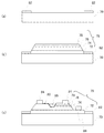
GaN系半導体を用いた縦型構造を有する半導体装置を製造する際、GaN系半導体装置に開口部を形成する際の工程(従来技術1)を説明する。図1は従来技術1の製造工程の断面図である。図1(a)において、基板100上にGaN系半導体層108としてドリフト層102、電子制御層104およびコンタクト層106を形成する。
A process (prior art 1) for forming an opening in a GaN-based semiconductor device when manufacturing a semiconductor device having a vertical structure using a GaN-based semiconductor will be described. FIG. 1 is a cross-sectional view of the manufacturing process of the prior art 1. In FIG. 1A, a
図1(b)において、所定領域を開口したフォトレジスト120を形成する。図1(c)において、フォトレジスト120をマスクにチャネル層106をCl2を用いドライエッチングし、チャネル層106に開口部を形成する。開口部にゲート電極112を形成し、チャネル層106上にソース電極110を形成する。このようにGaN系半導体層108にエッチングにより開口部を形成していた。
In FIG. 1B, a
さらに、GaN系半導体層を形成する技術として以下の技術(従来技術2)が開示されている。特許文献1では、GaN系半導体と異なる基板上にGaN系半導体からなる下地層を形成し、下地層上に部分的に保護膜を形成する。下地層から保護膜の上部に至るまでGaN系半導体層を形成する技術が開示されている。特許文献2においては、基板上にストライプ状のマスクを形成し、マスクを覆うようにGaN系半導体層を形成する技術が開示されている。
しかしながら、従来技術2においては、例えば、サファイア基板やSiC基板に厚いドリフト層を有するGaN系半導体を形成した場合、基板に反りが発生する。その結果、基板やGaN系半導体層にクラックが発生する。また半導体装置の製造工程において、露光工程の位置あわせ精度が低下する。
However, in the
さらに、従来技術1においては、GaN系半導体層に開口部を形成する際、コンタクト層106の開口部側面や電子制御層104の開口部下部にダメージが導入される。GaN系半導体層の導電領域においては、ダメージにより半導体表面や半導体中にトラップ準位が発生し、キャリアが不活性化し電子やホール濃度が低下してしまう。また、GaN系半導体層の絶縁領域においては、ダメージにより発生したトラップ準位によりリーク電流が流れる。これらにより、半導体装置の電気的特性が劣化してしまう。
Further, in the prior art 1, when the opening is formed in the GaN-based semiconductor layer, damage is introduced into the side surface of the opening of the
本発明は、基板の反りを防ぎ、GaN半導体層のクラックや製造工程における位置合わせ精度の低下を防止すること、若しくはGaN系半導体層に開口部を形成する際のダメージを防ぎ、電気的特性が劣化を防ぐことが可能な半導体装置の製造方法を提供することを目的とする。 The present invention prevents the warpage of the substrate, prevents the crack of the GaN semiconductor layer and the deterioration of the alignment accuracy in the manufacturing process, or prevents the damage when forming the opening in the GaN-based semiconductor layer, and has the electrical characteristics. It is an object to provide a method for manufacturing a semiconductor device capable of preventing deterioration.
本発明は、第1の面と前記第1の面と反対側の第2の面とを有する基板の、前記第1の面上にSiCまたはGaNからなる第1の半導体層を形成する工程と、前記第1の半導体層上をAlNまたはAlGaN層で覆う工程と、前記AlNまたはAlGaN層をパターニングして、前記第1の半導体層を露出する開口部を形成する工程と、前記開口部には成長せず前記パターニングされたAlNまたはAlGaN層上に成長するように、前記AlNまたはAlGaN層をシード層として、側面及び上面を有するGaN系半導体層を選択成長する工程と、前記GaN系半導体層の前記側面にゲート電極を、前記GaN系半導体層の前記上面にソース電極またはエミッタ電極を、前記第1の半導体層の前記GaN系半導体層が形成された側の面上あるいは前記基板の前記第2の面上にドレイン電極またはコレクタ電極を、形成する工程と、を有する半導体装置の製造方法である。本発明によれば、基板の反りを防ぎ、GaN半導体層のクラックや製造工程における位置合わせ精度の低下を防止し、若しくはGaN系半導体層に開口部を形成する際のダメージを防ぎ、電気的特性が劣化を防ぐことが可能な半導体装置の製造方法を提供することができる。 The present invention includes a step of forming a first semiconductor layer made of SiC or GaN on the first surface of a substrate having a first surface and a second surface opposite to the first surface. a step of covering the first semiconductor layer on at AlN or AlGaN layer, patterning the AlN or AlGaN layer, and forming an opening exposing the first semiconductor layer, the opening Selectively growing a GaN-based semiconductor layer having a side surface and an upper surface using the AlN or AlGaN layer as a seed layer so as to grow on the patterned AlN or AlGaN layer without growing ; A gate electrode on the side surface, a source electrode or an emitter electrode on the top surface of the GaN-based semiconductor layer, and a surface of the first semiconductor layer on the side where the GaN-based semiconductor layer is formed. There is a drain electrode or a collector electrode on the second surface of the substrate, and forming a manufacturing method of a semiconductor device having a. According to the present invention, the warpage of the substrate is prevented, the crack of the GaN semiconductor layer and the alignment accuracy in the manufacturing process are prevented, or the damage when forming the opening in the GaN-based semiconductor layer is prevented, and the electrical characteristics It is possible to provide a method for manufacturing a semiconductor device capable of preventing deterioration.
本発明は、前記基板はSiC基板、サファイア基板、Si基板およびGaNを含む半導体基板のいずれかである半導体装置の製造方法とすることができる。
The present invention can be a semiconductor device manufacturing method in which the substrate is any one of a SiC substrate, a sapphire substrate, a Si substrate, and a semiconductor substrate containing GaN .
本発明によれば、基板の反りを防ぎ、GaN半導体層のクラックや製造工程における位置合わせ精度の低下を防止し、若しくはGaN系半導体層に開口部を形成する際のダメージを防ぎ、電気的特性が劣化を防ぐことが可能となる。 According to the present invention, the warpage of the substrate is prevented, the crack of the GaN semiconductor layer and the alignment accuracy in the manufacturing process are prevented, or the damage when forming the opening in the GaN-based semiconductor layer is prevented, and the electrical characteristics It is possible to prevent deterioration.
従来技術における、基板が反る原因としては、各材料の熱膨張率の差がある。表1はGaN系半導体であるGaN、AlN、および基板として使用されるSiC、Siおよびサファイアの熱膨張率である。SiおよびサファイアはGaN、AlNの熱膨張率と大きく異なる。SiCはGaN、AlNの熱膨張率から10%程度異なっている。GaN系半導体層の成膜は通常1000℃前後で行われるため、10%程度の熱膨張率の差であっても、常温においては熱膨張率に起因した応力は大きくなる。基板にこの応力にGaN系半導体層の膜厚の積の力が加わり、基板は大きく反ってしまう。 As a cause of warping of the substrate in the prior art, there is a difference in thermal expansion coefficient of each material. Table 1 shows thermal expansion coefficients of GaN-based semiconductors, GaN, AlN, and SiC, Si, and sapphire used as substrates. Si and sapphire are greatly different from the thermal expansion coefficients of GaN and AlN. SiC differs by about 10% from the thermal expansion coefficients of GaN and AlN. Since the film formation of the GaN-based semiconductor layer is usually performed at around 1000 ° C., even if the difference in thermal expansion coefficient is about 10%, the stress due to the thermal expansion coefficient becomes large at room temperature. The force of the product of the film thickness of the GaN-based semiconductor layer is applied to the stress on the substrate, and the substrate is greatly warped.

そこで、基板に図2(a)のようなパターンのマスク層90を形成し島状の開口部92にのみGaN系半導体層を選択的に成長させる。これにより、基板とGaN系半導体層の熱膨張率の差に起因した応力が発生したとしても基板全体が反ることはない。よって、基板の反りに起因するGaN半導体層のクラックや製造工程における位置合わせ精度の低下を防止することができる。さらに、図2(b)のように、マスク層をマスクとした選択成長でGaN系半導体層を形成することにより、従来技術1のような開口部を形成する際のエッチングダメージによる電気的特性が劣化を防止することができる。
Therefore, a
マスク層のパターンは、基板の反りを防止する効果があればよい。図2(a)の四角形の島状以外にも、例えばストライプ、三角形、六角形、八角形、十二角形であってもよい。また、マスク層はGaN系半導体層が成膜し難い材料であればよく、例えば窒化珪素膜層、酸化チタン膜層、酸化ジルコニウム膜層であってもよい。マスク層と基板との熱膨張率の差によっても基板は反るため、マスク層の膜厚は100nm以下が好ましい。 The mask layer pattern only needs to have an effect of preventing the substrate from warping. In addition to the rectangular island shape of FIG. 2A, for example, a stripe, a triangle, a hexagon, an octagon, and a dodecagon may be used. The mask layer may be any material that is difficult to form a GaN-based semiconductor layer, and may be, for example, a silicon nitride film layer, a titanium oxide film layer, or a zirconium oxide film layer. Since the substrate is warped also by the difference in thermal expansion coefficient between the mask layer and the substrate, the thickness of the mask layer is preferably 100 nm or less.
サファイア(0001)基板上に、MOCVD法を用い、マスク層92をマスクとして領域90に選択的にGaN系半導体層を成長するときの成長条件を表2に示す。各条件A、B、C、DおよびEの温度、NH3流量、TMG(Trimethylgallium)流量に対する(11−22)ファセット成長比を示している。(11−22)ファセット成長比は、(11−22)の成長面積の全成長面積に対する比である。
Table 2 shows the growth conditions when a GaN-based semiconductor layer is selectively grown on the
(11−22)ファセット成長比が0%である条件Aにおいては、GaN系半導体層は(11−22)面に成長しないため、(0001)面に平面に成長(C面成長)が進む。(11−22)ファセット成長比が100%である条件Eにおいては、(11−22)面に成長が進むため、(0001)面の面積が縮小する成長が進む。このように、成長条件によって、ファセット成長、C面成長あるいはその中間の成長を選択することができる。 Under the condition A where the (11-22) facet growth ratio is 0%, since the GaN-based semiconductor layer does not grow on the (11-22) plane, the growth proceeds in a plane (C plane growth) on the (0001) plane. Under the condition E where the (11-22) facet growth ratio is 100%, the growth proceeds to the (11-22) plane, so that the growth of reducing the area of the (0001) plane proceeds. As described above, facet growth, C-plane growth, or an intermediate growth can be selected depending on the growth conditions.
以下、図面を参照し本発明の実施例を説明する。 Embodiments of the present invention will be described below with reference to the drawings.
実施例1は、基板上に選択的にGaN系半導体層を形成し、トランジスタを形成する例である。図3は実施例1の製造工程の断面図である。図3(a)において、サファイア基板70上にマスク層82として酸化シリコン膜を例えばCVD法により形成し、所定領域をエッチングする。これにより、開口部を有するマスク層82が形成される。このときのパターンは例えば図2(a)と同様である。
Example 1 is an example in which a GaN-based semiconductor layer is selectively formed on a substrate to form a transistor. FIG. 3 is a cross-sectional view of the manufacturing process of the first embodiment. In FIG. 3A, a silicon oxide film is formed as a
図3(b)において、マスク膜層82をマスクに、マスク層82以外の基板70上に、GaN系半導体層79として、n型のGaNバッファ層72、n型のGaNドリフト層74、p型の電子制御層76およびn型のGaNコンタクト層78をMOCVD法で形成する。このときの成長条件は、例えば表2の条件Aとする。
3B, using the
図3(c)において所定領域にドリフト層74に至る開口部をCl2のドライエッチングにより形成する。開口部を覆うようにAlNキャップ層80をMOCVD法を用い形成する。キャップ層の所定領域を除去し、ソース電極84を例えばTi/Alを用い形成する。ドリフト層74に至る開口部上にキャップ層を介しゲート電極86をNi/Auを形成する。所定領域をドリフト層74まで除去し、ドレイン電極88を例えばTi/Alで形成する。
In FIG. 3C, an opening reaching the
実施例1は、電子が、ソース電極84からコンタクト層78、電子制御層76のキャップ層80界面を通りドリフト層74に縦方向に流れドレイン電極88に至る電子がゲート電極86に制御されトランジスタ動作をする。
In the first embodiment, electrons flow from the
実施例1においては、GaN系半導体層79を島状の領域に形成することにより、基板70とGaN系半導体層79の熱膨張率の差に起因した基板70の反りを防止し、GaN半導体層のクラックや製造工程における位置合わせ精度の低下を防止することができる。
In Example 1, the GaN-based
実施例2は縦型FETの例である。実施例2に係る縦型FETの製造工程の断面図を図4に示す。図4(a)において、基板厚として400μmを有するn型キャリア濃度が1×1019cm−3のSiC基板10上に、第1の半導体層15として、500nmの膜厚を有するn型キャリア濃度が2×1019cm−3のGaNバッファ層12、10μmの膜厚を有するn型キャリア濃度が2×1016cm−3のGaNドリフト層14をMOCVD法で形成する。すなわち、第1の半導体層15はn型の基板10上にn型の半導体層である。
Example 2 is an example of a vertical FET. FIG. 4 shows a cross-sectional view of the manufacturing process of the vertical FET according to the second embodiment. In FIG. 4A, an n-type carrier concentration having a thickness of 500 nm as the
ドリフト層上に、酸化シリコン膜を例えばCVD法で形成し、所定領域を除去し、開口部を有するマスク層26を形成する。マスク層26は例えば図2(b)のよう島状に形成する。
A silicon oxide film is formed on the drift layer by, for example, a CVD method, a predetermined region is removed, and a
図4(b)において、マスク膜26をマスクに、マスク層以外の領域のドリフト層14上に、GaN系半導体層25として、100nmの膜厚を有するn型キャリア濃度が10×1016cm−3のGaNスペーサ層18、100nmの膜厚を有するp型キャリア濃度が1×1017cm−3の電子制御層20、100nmの膜厚を有するn型キャリア濃度が2×1019cm−3GaNコンタクト層22を例えばMOCVD法を用い形成する。このとき、GaN系半導体層25は、マスク層26が存在していない部分に選択的に形成することができる。これにより、GaN系半導体層25は開口部28を有する。GaN系半導体層25の成長は、例えば、表2の条件Eで行う。これにより開口部28の側面は、(11−22)面を有する斜面となる。開口部28を覆うようにAlNキャップ層24を10nm形成する。
In FIG. 4B, the n-type carrier concentration having a thickness of 100 nm is 10 × 10 16 cm − as the GaN-based
図4(c)において、所定領域のキャップ層24を除去した後、GaNコンタクト層22上にソース電極30を例えばTi/Alを用い形成する。開口部28のキャップ層24上にゲート電極32を例えばNi/Auを用い形成する。すなわち、ゲート電極32をGaN系半導体層25の開口部28の側面にキャップ層24を介し形成する。基板10を基板厚100μmまで研磨し背面に例えばNi/Alを用いドレイン電極34を形成する。すなわち、ドリフト層14のGaN系半導体層25と相対する面に接続されたドレイン電極34を形成する。以上により実施例2に係るトランジスタが完成する。この場合、GaN系半導体層25と同じ面にドレイン電極を形成することも可能である。
4C, after removing the
実施例2においては、電子が、ソース電極30からコンタクト層22、電子制御層20のキャップ層24界面、スペーサ層18を通りドリフト層14に縦方向に流れドレイン電極34に至る電子がゲート電極32に制御されトランジスタ動作をする
In the second embodiment, electrons flow from the
実施例2においては、GaN系半導体装置を島状の領域に形成することにより、基板10とGaN系半導体装置の熱膨張率の差に起因した基板10の反りを防止し、GaN半導体層のクラックや製造工程における位置合わせ精度の低下を防止することができる。さらに、ゲート電極32を形成するためGaN系半導体層25に形成された開口部28を、GaN系半導体層25を選択的に形成することにより設けている。よって、GaN系半導体層25側部へ導入されるエッチング起因のダメージを防止できる。チャネル層20のキャップ層24の界面は電子が流れる領域である。従来技術のようにドライエッチングで開口部28を形成すると、キャップ層24やチャネル層20にダメージが導入され、トランジスタの電気的特性は著しく劣化してしまう。実施例2においては、このような電気的特性の劣化を防止することができる。
In the second embodiment, the warpage of the
さらに、GaN系半導体層25の成長条件を、例えば表2の条件Eとすることにより開口部28の側面は(11−22)面となる。これにより、開口部28の斜面の角度を再現性よく製造することができる。縦型FETにおいては、開口部28の側面の角度によりゲート長が決まるため、側面の角度は電気的特性に大きく影響する。よって、実施例2においては、電気的特性の再現性を高めることもできる。開口部28の側面の角度は、ファセット成長比を所望になるように選択することにより、所望の傾きを得ることができる。
Further, when the growth condition of the GaN-based
実施例1の変形例1について説明する。変形例1はマスク層の代わりにシード層16としてAlNまたはAlGaNを用いた例である。変形例1に係るトランジスタの製造工程の断面図を図5に示す。図5(a)において、実施例2同様、SiC基板10上に第1の半導体層15をエピタキシャル成長にて形成する。さらにAlNまたはAlGaN層(AlNを含む半導体層)をMOCVD法により形成し、所定領域をエッチングで除去する。これによりシード層16を形成する。すなわち、シード層16を形成する前に第1の半導体層15の表面がAlNを含む半導体層で覆われている。シード層16のパターンは図2(c)のように島のマスク層と逆のパターンに形成する。
A first modification of the first embodiment will be described. Modification 1 is an example in which AlN or AlGaN is used as the
図5(b)において、パターン化したシード層16を用いて、シード層16上にGaN系半導体層25をMOCVD法を用い選択的に形成する。このとき、AlGaN上には成長するが、GaN上には成長し難い成長条件でGaN系半導体層を形成する。成長条件は表2の条件Eとした。これにより、シード層16上にGaN系半導体層25が形成される。GaN系半導体層25の構成は実施例2と同じである。その後、実施例2と同じ製造工程により図5(c)のトランジスタが完成する。
In FIG. 5B, using the patterned
変形例1においては、実施例2と同様に、GaN半導体装置のクラックや製造工程における位置合わせ精度の低下の防止、トランジスタの電気的特性の劣化の防止、トランジスタの電気的特性の再現性向上という効果が得られる。さらに、シード層16としてAlGaN層を用いシード層16上に選択的にGaN系半導体層25を形成しているため、マスク層16のパターン形成時のエッチングに曝されていない領域にGaN系半導体層25を成長することができる。これより結晶性のよいGaN半導体層25を形成することができる。
In the first modification, as in the second embodiment, the crack of the GaN semiconductor device and the lowering of the alignment accuracy in the manufacturing process are prevented, the deterioration of the electric characteristics of the transistor, and the reproducibility of the electric characteristics of the transistor are improved. An effect is obtained. Furthermore, since an AlGaN layer is used as the
次に、変形例2について説明する。変形例2はSiCドリフト層を有する例である。変形例2に係るトランジスタの製造工程の断面図を図6に示す。図6(a)において、基板厚として400μmを有するn型キャリア濃度が1×1019cm−3のSiC基板10a上に、第1の半導体層15aとして500nmの膜厚を有するn型キャリア濃度が2×1019cm−3のSiCバッファ層12a、10μmの膜厚を有するn型キャリア濃度が2×1016cm−3のSiCドリフト層14aをCVD法により形成する。ドリフト層14a上に、酸化シリコン膜を例えばCVD法で形成し、所定領域を除去し、開口部を有するマスク層26として酸化シリコン膜層を形成する。マスク層26は例えば図2(b)のように形成する。
Next,
図6(b)において、マスク層26をマスクに、ドリフト層14a上にGaN系半導体層25をMOCVD法を用い選択的に形成する。GaN系半導体層25の層構成および成長方法は実施例2と同じである。その後、実施例2と同じ製造工程により図6(c)のトランジスタが完成する。SiCドリフト層14aを有する変形例2においても、実施例2と同様に、GaN半導体層のクラックや製造工程における位置合わせ精度の低下の防止、トランジスタの電気的特性の劣化の防止、トランジスタの電気的特性の再現性向上という効果が得られる。また変形例1のように、シード層としてAlGaN層を用いシード層上に選択的にGaN系半導体層を形成することもできる。この場合も変形例1と同様に、結晶性のよいGaN半導体層25が得られるという効果が得られる。
In FIG. 6B, using the
実施例3はIGBT(Insulated Gate Bipolar Transistor)の例である。図7に実施例3に係るトランジスタの製造工程の断面図を示す。図7(a)において、p型のSiC基板40の(0001)面上に、第1の半導体層45として、p型GaNバッファ層42、n型GaNドリフト層44をMOCVD法により形成する。すなわち、第1の半導体層45は、p型の基板40上に形成されたp型半導体層とその上に形成されたn型半導体層である。ドリフト層44上に、酸化シリコン膜を例えばCVD法で形成し、所定領域を除去し、開口部を有するマスク層56として酸化シリコン膜層を形成する。マスク層56は例えば図2(b)のように形成する。
Example 3 is an example of an IGBT (Insulated Gate Bipolar Transistor). FIG. 7 is a cross-sectional view of the manufacturing process of the transistor according to the third embodiment. 7A, a p-type
図7(b)において、マスク膜56をマスクに、マスク層56以外の領域のドリフト層44上に、GaN系半導体層45として、n型GaNスペーサ層48、p型GaN電子制御層50、n型GaNコンタクト層52を例えばMOCVD法を用い形成する。このとき、GaN系半導体層55は、マスク層56の開口部に選択的に形成することができる。これにより、GaN系半導体層45は開口部58を有する。GaN系半導体層45の成長は、例えば、表2の条件Eで行う。これにより開口部58の側面は、(11−22)面を有する斜面となる。開口部58を覆うようにAlNまたはAlGaNキャップ層54をMOCVD法またはMBE法を用い形成する。
7B, using the
図7(c)において、所定領域のキャップ層54を除去した後、コンタクト層52上にエミッタ電極60を例えばTi/Alを用い形成する。開口部58のキャップ層54上にゲート電極62を例えばNi/Auを用い形成する。すなわち、ゲート電極62をGaN系半導体層55の開口部58の側面にキャップ層54を介し形成する。基板30の背面に例えばNi/Auを用いコレクタ電極64を形成する。すなわち、ドリフト層44のGaN系半導体層55と相対する面に接続されたコレクタ電極64を形成する。以上により実施例3に係るトランジスタが完成する。
In FIG. 7C, after removing the
実施例3においては、GaNドリフト層を有するIGBTにおいても、実施例2と同様に、GaN半導体層のクラックや製造工程における位置合わせ精度の低下の防止、トランジスタの電気的特性の劣化の防止という効果が得られる。また、開口部58の側面の角度を再現性良く製造することができる。これにより、IGBTの電気特性を再現性良く製造することができる。
In the third embodiment, even in the IGBT having the GaN drift layer, as in the second embodiment, the effect of preventing the crack of the GaN semiconductor layer, the deterioration of the alignment accuracy in the manufacturing process, and the deterioration of the electrical characteristics of the transistor. Is obtained. Moreover, the angle of the side surface of the
変形例1はSiCドリフト層を有するIGBTの例である。図8に変形例1に係るトランジスタの製造工程の断面図を示す。図8(a)において、p型のSiC基板40aの(0001)面上に、第1の半導体層45aとして、p型SiCバッファ層42a、n型SiCドリフト層44aをCVD法により形成する。ドリフト層44a上に、酸化シリコン膜を例えばCVD法で形成し、所定領域を除去し、開口部を有するマスク層56を形成する。マスク層56は例えば図2(b)のように形成する。
Modification 1 is an example of an IGBT having a SiC drift layer. FIG. 8 shows a cross-sectional view of a manufacturing process of a transistor according to the first modification. In FIG. 8A, a p-type
図8(b)において、マスク膜56をマスクに、マスク層以外の領域のドリフト層44a上に、GaN系半導体層55をマスク層56の開口部に選択的に形成する。GaN系半導体層55の層構成および成長方法は実施例4と同じである。その後、実施例2と同じ製造工程により図8(c)のトランジスタが完成する。SiCドリフト層を有する変形例1においても、実施例3と同様に、GaN半導体層のクラックや製造工程における位置合わせ精度の低下の防止、トランジスタの電気的特性の劣化の防止、トランジスタの電気的特性の再現性向上という効果が得られる。
8B, using the
実施例2、実施例3およびその変形例においては、電子制御層にGaN系半導体層として、例えばGaN、AlNおよびInNの少なくとも1つからなる結晶層または混晶層を用いることによりオン抵抗を低くできる。これらの半導体は移動度が高いためである。さらに、キャップ層として、チャネル層よりバンドギャップの大きなGaN系半導体層を用いることにより、さらに電子制御性を良くしリーク電流を低くすることができる。基板10、40はSiC基板以外にも、サファイア基板、Si基板またはGaNを含む半導体基板を用いることもできる。これにより、結晶性の良い成長が可能となる。さらに、GaN系半導体層の形成はMOCVD法またはMBE法を用いることにより、より結晶性の良いGaN系半導体層が形成できる。
In the second embodiment, the third embodiment, and the modifications thereof, the on-resistance is lowered by using, for example, a crystal layer or mixed crystal layer made of at least one of GaN, AlN, and InN as the GaN-based semiconductor layer in the electronic control layer. it can. This is because these semiconductors have high mobility. Furthermore, by using a GaN-based semiconductor layer having a larger band gap than the channel layer as the cap layer, the electronic controllability can be further improved and the leakage current can be reduced. As the
10、40 SiC基板
10a、40a SiC基板
12、42 GaNバッファ層
12a、42a SiCバッファ層
14、44 GaNドリフト層
14a、44a SiCドリフト層
15、15a、45、45a 第1の半導体層
16 シード層
18 GaNスペーサ層
20 GaN電子制御層
22 GaNコンタクト層
24 キャップ層
25、55 GaN系半導体層
26、56 マスク層
28、58 開口部
30 ソース電極
32 ゲート電極
34 ドレイン電極
48 GaNスペーサ層
50 GaN電子制御層
52 GaNコンタクト層
54 キャップ層
60 エミッタ電極
62 ゲート電極
64 コレクタ電極
70 サファイア基板
72 バッファ層
74 ドリフト層
76 電子制御層
78 コンタクト層
80 キャップ層
82 マスク層
84 ソース電極
86 ゲート電極
88 ドレイン電極
90 開口部
92 マスク層
10, 40
Claims (2)
前記第1の半導体層上をAlNまたはAlGaN層で覆う工程と、
前記AlNまたはAlGaN層をパターニングして、前記第1の半導体層を露出する開口部を形成する工程と、
前記開口部には成長せず前記パターニングされたAlNまたはAlGaN層上に成長するように、前記AlNまたはAlGaN層をシード層として、側面及び上面を有するGaN系半導体層を選択成長する工程と、
前記GaN系半導体層の前記側面にゲート電極を、前記GaN系半導体層の前記上面にソース電極またはエミッタ電極を、前記第1の半導体層の前記GaN系半導体層が形成された側の面上あるいは前記基板の前記第2の面上にドレイン電極またはコレクタ電極を、形成する工程と、
を有する半導体装置の製造方法。 Forming a first semiconductor layer made of SiC or GaN on the first surface of a substrate having a first surface and a second surface opposite to the first surface;
Covering the first semiconductor layer with an AlN or AlGaN layer;
Patterning the AlN or AlGaN layer to form an opening exposing the first semiconductor layer ;
Selectively growing a GaN-based semiconductor layer having a side surface and an upper surface using the AlN or AlGaN layer as a seed layer so as to grow on the patterned AlN or AlGaN layer without growing in the opening;
A gate electrode on the side surface of the GaN-based semiconductor layer , a source electrode or an emitter electrode on the upper surface of the GaN-based semiconductor layer , or a surface on the side of the first semiconductor layer on which the GaN-based semiconductor layer is formed or Forming a drain electrode or a collector electrode on the second surface of the substrate ;
A method for manufacturing a semiconductor device comprising :
Priority Applications (2)
| Application Number | Priority Date | Filing Date | Title |
|---|---|---|---|
| JP2005105163A JP4986406B2 (en) | 2005-03-31 | 2005-03-31 | Manufacturing method of semiconductor device |
| US11/392,549 US7728353B2 (en) | 2005-03-31 | 2006-03-30 | Semiconductor device in which GaN-based semiconductor layer is selectively formed |
Applications Claiming Priority (1)
| Application Number | Priority Date | Filing Date | Title |
|---|---|---|---|
| JP2005105163A JP4986406B2 (en) | 2005-03-31 | 2005-03-31 | Manufacturing method of semiconductor device |
Publications (3)
| Publication Number | Publication Date |
|---|---|
| JP2006286954A JP2006286954A (en) | 2006-10-19 |
| JP2006286954A5 JP2006286954A5 (en) | 2008-05-08 |
| JP4986406B2 true JP4986406B2 (en) | 2012-07-25 |
Family
ID=37069249
Family Applications (1)
| Application Number | Title | Priority Date | Filing Date |
|---|---|---|---|
| JP2005105163A Expired - Fee Related JP4986406B2 (en) | 2005-03-31 | 2005-03-31 | Manufacturing method of semiconductor device |
Country Status (2)
| Country | Link |
|---|---|
| US (1) | US7728353B2 (en) |
| JP (1) | JP4986406B2 (en) |
Families Citing this family (27)
| Publication number | Priority date | Publication date | Assignee | Title |
|---|---|---|---|---|
| TWI226139B (en) | 2002-01-31 | 2005-01-01 | Osram Opto Semiconductors Gmbh | Method to manufacture a semiconductor-component |
| US20060180804A1 (en) * | 2003-01-31 | 2006-08-17 | Peter Stauss | Thin-film semiconductor component and production method for said component |
| US8524573B2 (en) | 2003-01-31 | 2013-09-03 | Osram Opto Semiconductors Gmbh | Method for separating a semiconductor layer from a substrate by irradiating with laser pulses |
| JP5051980B2 (en) * | 2005-03-31 | 2012-10-17 | 住友電工デバイス・イノベーション株式会社 | Semiconductor device |
| ATE526975T1 (en) * | 2005-10-07 | 2011-10-15 | California Inst Of Techn | PKR ACTIVATION USING HYBRIDIZATION CHAIN REACTION |
| JP2008078604A (en) * | 2006-08-24 | 2008-04-03 | Rohm Co Ltd | Mis field effect transistor and method for manufacturing the same |
| JP5134797B2 (en) * | 2006-09-13 | 2013-01-30 | ローム株式会社 | GaN-based semiconductor device, manufacturing method thereof, and GaN-based semiconductor device |
| US8421119B2 (en) * | 2006-09-13 | 2013-04-16 | Rohm Co., Ltd. | GaN related compound semiconductor element and process for producing the same and device having the same |
| JP4999065B2 (en) * | 2006-11-09 | 2012-08-15 | 古河電気工業株式会社 | Power semiconductor element |
| JP5189771B2 (en) * | 2007-02-01 | 2013-04-24 | ローム株式会社 | GaN-based semiconductor devices |
| WO2008099843A1 (en) * | 2007-02-14 | 2008-08-21 | Rohm Co., Ltd. | Nitride semiconductor element and method for manufacturing nitride semiconductor element |
| JP2008205199A (en) * | 2007-02-20 | 2008-09-04 | Rohm Co Ltd | METHOD OF MANUFACTURING GaN-BASED SEMICONDUCTOR ELEMENT |
| JP2008226914A (en) * | 2007-03-08 | 2008-09-25 | Rohm Co Ltd | Gan-based semiconductor element |
| JP2008227073A (en) * | 2007-03-12 | 2008-09-25 | Rohm Co Ltd | Formation method of nitride semiconductor laminate structure and manufacturing method of nitride semiconductor element |
| JP5252813B2 (en) * | 2007-03-15 | 2013-07-31 | 株式会社豊田中央研究所 | Manufacturing method of semiconductor device |
| FR2924270B1 (en) * | 2007-11-27 | 2010-08-27 | Picogiga Internat | METHOD FOR MANUFACTURING AN ELECTRONIC DEVICE |
| US9048302B2 (en) * | 2008-01-11 | 2015-06-02 | The Furukawa Electric Co., Ltd | Field effect transistor having semiconductor operating layer formed with an inclined side wall |
| DE112010001560B4 (en) * | 2009-04-08 | 2020-08-13 | Efficient Power Conversion Corporation | GaN-FLIP-CHIP power transistor with electrically isolated back |
| JP5531538B2 (en) * | 2009-09-30 | 2014-06-25 | 住友電気工業株式会社 | Heterojunction transistor and method of manufacturing heterojunction transistor |
| JP2011210780A (en) * | 2010-03-29 | 2011-10-20 | Oki Electric Industry Co Ltd | GaN-MIS TRANSISTOR, GaN-IGBT AND METHOD FOR MANUFACTURING THEM |
| JP2012160746A (en) * | 2012-03-26 | 2012-08-23 | Furukawa Electric Co Ltd:The | Power semiconductor element |
| JP6170300B2 (en) * | 2013-01-08 | 2017-07-26 | 住友化学株式会社 | Nitride semiconductor devices |
| US9865725B2 (en) * | 2015-04-14 | 2018-01-09 | Hrl Laboratories, Llc | III-nitride transistor with trench gate |
| JP6755892B2 (en) * | 2016-02-08 | 2020-09-16 | パナソニック株式会社 | Semiconductor device |
| US20200194615A1 (en) * | 2017-05-05 | 2020-06-18 | The Regents Of The University Of California | Method of removing a substrate |
| DE102021204293A1 (en) * | 2021-04-29 | 2022-11-03 | Robert Bosch Gesellschaft mit beschränkter Haftung | VERTICAL TRANSISTOR AND METHOD OF MAKING THE SAME |
| WO2023162521A1 (en) * | 2022-02-22 | 2023-08-31 | ローム株式会社 | Nitride semiconductor device and manufacturing method therefor |
Family Cites Families (20)
| Publication number | Priority date | Publication date | Assignee | Title |
|---|---|---|---|---|
| JPS647516A (en) * | 1987-03-27 | 1989-01-11 | Canon Kk | Manufacture of compound semiconductor and semiconductor device using thereof |
| JPH0492439A (en) * | 1990-08-08 | 1992-03-25 | Hitachi Ltd | Manufacture of semiconductor integrated circuit device |
| US5557115A (en) * | 1994-08-11 | 1996-09-17 | Rohm Co. Ltd. | Light emitting semiconductor device with sub-mount |
| JPH10223901A (en) * | 1996-12-04 | 1998-08-21 | Sony Corp | Field effect transistor and manufacture of the same |
| JP3577880B2 (en) * | 1997-03-26 | 2004-10-20 | 住友化学工業株式会社 | Method for manufacturing group 3-5 compound semiconductor |
| JP3876518B2 (en) | 1998-03-05 | 2007-01-31 | 日亜化学工業株式会社 | Nitride semiconductor substrate manufacturing method and nitride semiconductor substrate |
| JP2000349338A (en) | 1998-09-30 | 2000-12-15 | Nec Corp | GaN CRYSTAL FILM, AND III-FAMILY ELEMENT NITRIDE SEMICONDUCTOR WAFER AND ITS MANUFACTURE |
| JP2000208760A (en) * | 1999-01-13 | 2000-07-28 | Furukawa Electric Co Ltd:The | Field effect transistor |
| JP4667556B2 (en) * | 2000-02-18 | 2011-04-13 | 古河電気工業株式会社 | Vertical GaN-based field effect transistor, bipolar transistor and vertical GaN-based field effect transistor manufacturing method |
| JP3966763B2 (en) * | 2001-06-01 | 2007-08-29 | 古河電気工業株式会社 | GaN-based semiconductor device |
| JP3815335B2 (en) * | 2002-01-18 | 2006-08-30 | ソニー株式会社 | Semiconductor light emitting device and manufacturing method thereof |
| JP4865189B2 (en) * | 2002-02-21 | 2012-02-01 | 古河電気工業株式会社 | GaN-based field effect transistor |
| JP2003257997A (en) * | 2002-02-28 | 2003-09-12 | Sumitomo Electric Ind Ltd | Method for manufacturing gallium nitride system semiconductor |
| JP2003347315A (en) * | 2002-05-23 | 2003-12-05 | Sharp Corp | Semiconductor device, manufacturing method thereof, power amplifier, and radio communication system |
| US6830945B2 (en) * | 2002-09-16 | 2004-12-14 | Hrl Laboratories, Llc | Method for fabricating a non-planar nitride-based heterostructure field effect transistor |
| US7112860B2 (en) * | 2003-03-03 | 2006-09-26 | Cree, Inc. | Integrated nitride-based acoustic wave devices and methods of fabricating integrated nitride-based acoustic wave devices |
| JP2005005657A (en) * | 2003-06-09 | 2005-01-06 | Sc Technology Kk | Crystal layer structure of field effect transistor |
| US7439555B2 (en) * | 2003-12-05 | 2008-10-21 | International Rectifier Corporation | III-nitride semiconductor device with trench structure |
| US7382001B2 (en) * | 2004-01-23 | 2008-06-03 | International Rectifier Corporation | Enhancement mode III-nitride FET |
| JP4447413B2 (en) * | 2004-09-10 | 2010-04-07 | 株式会社神戸製鋼所 | Manufacturing method of semiconductor device |
-
2005
- 2005-03-31 JP JP2005105163A patent/JP4986406B2/en not_active Expired - Fee Related
-
2006
- 2006-03-30 US US11/392,549 patent/US7728353B2/en not_active Expired - Fee Related
Also Published As
| Publication number | Publication date |
|---|---|
| US7728353B2 (en) | 2010-06-01 |
| JP2006286954A (en) | 2006-10-19 |
| US20060220042A1 (en) | 2006-10-05 |
Similar Documents
| Publication | Publication Date | Title |
|---|---|---|
| JP4986406B2 (en) | Manufacturing method of semiconductor device | |
| CN110224019B (en) | Semiconductor device and manufacturing method thereof | |
| TWI431770B (en) | Semiconductor device and method for manufacturing the same | |
| JP5564791B2 (en) | Compound semiconductor device and manufacturing method thereof | |
| KR101108344B1 (en) | Methods of fabricating nitride-based transistors with a cap layer and a recessed gate | |
| JP5261945B2 (en) | Field effect semiconductor device and manufacturing method thereof | |
| US20080079009A1 (en) | Semiconductor device | |
| JP5780613B2 (en) | Semiconductor device having improved adhesion and method for manufacturing the same | |
| JP4786730B2 (en) | Field effect transistor and manufacturing method thereof | |
| JP4907929B2 (en) | Field effect semiconductor device and method for manufacturing field effect semiconductor device | |
| JP2008187173A (en) | Group iii nitride power semiconductor device | |
| TWI535007B (en) | Semiconductor device and manufacturing method thereof | |
| JP2011171639A (en) | Semiconductor device, semiconductor wafer, method of manufacturing semiconductor device, and method of manufacturing semiconductor wafer | |
| JP2007027440A (en) | Semiconductor device | |
| JP2013077638A (en) | Semiconductor device | |
| JP2010165783A (en) | Field effect transistor, and method of manufacturing the same | |
| KR20190112523A (en) | Heterostructure Field Effect Transistor and production method thereof | |
| EP4210113A1 (en) | Method for fabricating a high electron mobility transistor | |
| JP2008072083A (en) | Nitride semiconductor device and method for manufacturing same | |
| US9922936B1 (en) | Semiconductor lithography alignment feature with epitaxy blocker | |
| JP2007088186A (en) | Semiconductor device and its fabrication process | |
| KR101256465B1 (en) | Nitride baced semiconductor device and manufacturing method thereof | |
| JP2006179546A (en) | Semiconductor electronic device | |
| KR102261735B1 (en) | Hetero-junction transistor | |
| US10403496B2 (en) | Compound semiconductor substrate and method of forming a compound semiconductor substrate |
Legal Events
| Date | Code | Title | Description |
|---|---|---|---|
| A521 | Written amendment |
Free format text: JAPANESE INTERMEDIATE CODE: A523 Effective date: 20080317 |
|
| A621 | Written request for application examination |
Free format text: JAPANESE INTERMEDIATE CODE: A621 Effective date: 20080317 |
|
| A977 | Report on retrieval |
Free format text: JAPANESE INTERMEDIATE CODE: A971007 Effective date: 20111118 |
|
| A131 | Notification of reasons for refusal |
Free format text: JAPANESE INTERMEDIATE CODE: A131 Effective date: 20111206 |
|
| A521 | Written amendment |
Free format text: JAPANESE INTERMEDIATE CODE: A523 Effective date: 20120118 |
|
| A131 | Notification of reasons for refusal |
Free format text: JAPANESE INTERMEDIATE CODE: A131 Effective date: 20120214 |
|
| A521 | Written amendment |
Free format text: JAPANESE INTERMEDIATE CODE: A523 Effective date: 20120406 |
|
| TRDD | Decision of grant or rejection written | ||
| A01 | Written decision to grant a patent or to grant a registration (utility model) |
Free format text: JAPANESE INTERMEDIATE CODE: A01 Effective date: 20120424 |
|
| A01 | Written decision to grant a patent or to grant a registration (utility model) |
Free format text: JAPANESE INTERMEDIATE CODE: A01 |
|
| A61 | First payment of annual fees (during grant procedure) |
Free format text: JAPANESE INTERMEDIATE CODE: A61 Effective date: 20120424 |
|
| R150 | Certificate of patent or registration of utility model |
Free format text: JAPANESE INTERMEDIATE CODE: R150 |
|
| FPAY | Renewal fee payment (event date is renewal date of database) |
Free format text: PAYMENT UNTIL: 20150511 Year of fee payment: 3 |
|
| LAPS | Cancellation because of no payment of annual fees |