JP4961179B2 - Substrate processing apparatus and semiconductor device manufacturing method - Google Patents
Substrate processing apparatus and semiconductor device manufacturing method Download PDFInfo
- Publication number
- JP4961179B2 JP4961179B2 JP2006216028A JP2006216028A JP4961179B2 JP 4961179 B2 JP4961179 B2 JP 4961179B2 JP 2006216028 A JP2006216028 A JP 2006216028A JP 2006216028 A JP2006216028 A JP 2006216028A JP 4961179 B2 JP4961179 B2 JP 4961179B2
- Authority
- JP
- Japan
- Prior art keywords
- substrate
- wafer
- susceptor
- processing
- processing apparatus
- Prior art date
- Legal status (The legal status is an assumption and is not a legal conclusion. Google has not performed a legal analysis and makes no representation as to the accuracy of the status listed.)
- Active
Links
- 239000000758 substrate Substances 0.000 title claims description 120
- 238000012545 processing Methods 0.000 title claims description 111
- 239000004065 semiconductor Substances 0.000 title claims description 5
- 238000004519 manufacturing process Methods 0.000 title claims description 4
- 238000000034 method Methods 0.000 claims description 11
- 239000002245 particle Substances 0.000 description 45
- 239000007789 gas Substances 0.000 description 19
- 230000007246 mechanism Effects 0.000 description 16
- 230000002093 peripheral effect Effects 0.000 description 15
- 239000010453 quartz Substances 0.000 description 13
- VYPSYNLAJGMNEJ-UHFFFAOYSA-N silicon dioxide Inorganic materials O=[Si]=O VYPSYNLAJGMNEJ-UHFFFAOYSA-N 0.000 description 13
- 239000012495 reaction gas Substances 0.000 description 9
- 238000012546 transfer Methods 0.000 description 8
- 230000008569 process Effects 0.000 description 7
- 238000001179 sorption measurement Methods 0.000 description 7
- 239000010408 film Substances 0.000 description 5
- 239000003990 capacitor Substances 0.000 description 4
- 230000000694 effects Effects 0.000 description 4
- 230000005684 electric field Effects 0.000 description 4
- 230000003028 elevating effect Effects 0.000 description 4
- 238000010438 heat treatment Methods 0.000 description 4
- 238000012423 maintenance Methods 0.000 description 4
- 238000005259 measurement Methods 0.000 description 4
- 230000009467 reduction Effects 0.000 description 4
- 239000000919 ceramic Substances 0.000 description 3
- 239000000463 material Substances 0.000 description 3
- 239000007769 metal material Substances 0.000 description 3
- 230000015572 biosynthetic process Effects 0.000 description 2
- 230000000052 comparative effect Effects 0.000 description 2
- 230000007423 decrease Effects 0.000 description 2
- 238000009832 plasma treatment Methods 0.000 description 2
- 241001391944 Commicarpus scandens Species 0.000 description 1
- 241000135309 Processus Species 0.000 description 1
- XUIMIQQOPSSXEZ-UHFFFAOYSA-N Silicon Chemical compound [Si] XUIMIQQOPSSXEZ-UHFFFAOYSA-N 0.000 description 1
- 230000002411 adverse Effects 0.000 description 1
- 229910052783 alkali metal Inorganic materials 0.000 description 1
- 150000001340 alkali metals Chemical class 0.000 description 1
- 229910052784 alkaline earth metal Inorganic materials 0.000 description 1
- 150000001342 alkaline earth metals Chemical class 0.000 description 1
- 229910052782 aluminium Inorganic materials 0.000 description 1
- XAGFODPZIPBFFR-UHFFFAOYSA-N aluminium Chemical compound [Al] XAGFODPZIPBFFR-UHFFFAOYSA-N 0.000 description 1
- PNEYBMLMFCGWSK-UHFFFAOYSA-N aluminium oxide Inorganic materials [O-2].[O-2].[O-2].[Al+3].[Al+3] PNEYBMLMFCGWSK-UHFFFAOYSA-N 0.000 description 1
- VJBCNMFKFZIXHC-UHFFFAOYSA-N azanium;2-(4-methyl-5-oxo-4-propan-2-yl-1h-imidazol-2-yl)quinoline-3-carboxylate Chemical compound N.N1C(=O)C(C(C)C)(C)N=C1C1=NC2=CC=CC=C2C=C1C(O)=O VJBCNMFKFZIXHC-UHFFFAOYSA-N 0.000 description 1
- 239000002585 base Substances 0.000 description 1
- 238000011109 contamination Methods 0.000 description 1
- PMHQVHHXPFUNSP-UHFFFAOYSA-M copper(1+);methylsulfanylmethane;bromide Chemical compound Br[Cu].CSC PMHQVHHXPFUNSP-UHFFFAOYSA-M 0.000 description 1
- 125000004122 cyclic group Chemical group 0.000 description 1
- 238000010586 diagram Methods 0.000 description 1
- 239000010432 diamond Substances 0.000 description 1
- 229910003460 diamond Inorganic materials 0.000 description 1
- 238000009792 diffusion process Methods 0.000 description 1
- 239000006185 dispersion Substances 0.000 description 1
- 238000005530 etching Methods 0.000 description 1
- 239000011521 glass Substances 0.000 description 1
- 239000012535 impurity Substances 0.000 description 1
- 239000012212 insulator Substances 0.000 description 1
- 229910052751 metal Inorganic materials 0.000 description 1
- 239000002184 metal Substances 0.000 description 1
- 238000012986 modification Methods 0.000 description 1
- 230000004048 modification Effects 0.000 description 1
- 150000004767 nitrides Chemical class 0.000 description 1
- 230000003647 oxidation Effects 0.000 description 1
- 238000007254 oxidation reaction Methods 0.000 description 1
- TWNQGVIAIRXVLR-UHFFFAOYSA-N oxo(oxoalumanyloxy)alumane Chemical compound O=[Al]O[Al]=O TWNQGVIAIRXVLR-UHFFFAOYSA-N 0.000 description 1
- 238000007790 scraping Methods 0.000 description 1
- 229910052710 silicon Inorganic materials 0.000 description 1
- 239000010703 silicon Substances 0.000 description 1
- 238000002230 thermal chemical vapour deposition Methods 0.000 description 1
- 239000010409 thin film Substances 0.000 description 1
- 238000011282 treatment Methods 0.000 description 1
Images


Description
本発明は、処理容器内で基板をプラズマ処理する基板処理装置に関する。 The present invention relates to a substrate processing apparatus for plasma processing a substrate in a processing container.
従来のプラズマ処理する基板処理装置(以下、プラズマ処理装置という)には、最も一般的な容量結合型プラズマ処理装置、電界と磁界により高密度プラズマを生成できる変形マグネトロン型プラズマ処理装置等がある。この変形マグネトロン型プラズマ処理装置は、他の処理装置よりも高密度プラズマが得られる。 Conventional substrate processing apparatuses that perform plasma processing (hereinafter referred to as plasma processing apparatuses) include the most general capacitively coupled plasma processing apparatus and a modified magnetron plasma processing apparatus that can generate high-density plasma by an electric field and a magnetic field. This modified magnetron type plasma processing apparatus can obtain a higher density plasma than other processing apparatuses.
上記変形マグネトロン型プラズマ処理装置は、処理室と、処理室周囲に配置された筒状電極及び磁力線形成手段と、基板を保持するサセプタとを有する。サセプタはアース電極を有し、そのアース電極はコイル及びコンデンサを有する高周波整合器を介して接地される。従って、サセプタはサセプタ電極となっている。高周波整合器のコイル又はコンデンサによりサセプタのインピーダンスを変化させてサセプタ電位を調整し、筒状電極に高周波電力を印加しながら処理室に処理ガスとして反応ガスを供給して、プラズマ励起された反応ガスにより処理室内に配置された基板の表面をプラズマ処理する。 The modified magnetron type plasma processing apparatus includes a processing chamber, a cylindrical electrode and a magnetic force line forming unit disposed around the processing chamber, and a susceptor that holds a substrate. The susceptor has a ground electrode, and the ground electrode is grounded via a high-frequency matching unit having a coil and a capacitor. Therefore, the susceptor is a susceptor electrode. Plasma-excited reaction gas by adjusting the susceptor potential by changing the impedance of the susceptor with a coil or capacitor of a high-frequency matching unit, supplying a reaction gas as a processing gas to the processing chamber while applying high-frequency power to the cylindrical electrode Thus, the surface of the substrate disposed in the processing chamber is subjected to plasma processing.
しかしながら、上述した従来の基板処理装置では、アース電極を有するサセプタに基板を保持するために、特に基板に付着する異物(パーティクル)量が多い。この理由は、プラズマ生成過程で、アース電極による静電力により基板がサセプタに吸着される状態となる。このため基板に電荷が帯電し、パーティクルが基板に吸着されやすくなるからである。
本発明の課題は、上述した従来技術の問題点を解消して、基板に付着するパーティクルを低減することが可能な基板処理装置を提供することにある。
However, in the conventional substrate processing apparatus described above, the amount of foreign matter (particles) adhering to the substrate is particularly large in order to hold the substrate on the susceptor having the ground electrode. This is because the substrate is attracted to the susceptor by the electrostatic force generated by the ground electrode during the plasma generation process. For this reason, electric charges are charged on the substrate, and particles are easily adsorbed on the substrate.
An object of the present invention is to provide a substrate processing apparatus capable of solving the above-described problems of the prior art and reducing particles adhering to the substrate.
本発明の一態様によれば、プラズマにより基板を処理する処理容器と、前記処理容器の中に設けられアース電極を有するサセプタと、前記サセプタの上に設けられ少なくとも前記基板の周縁部を支持する支持部を有する基板載置体とを備えた基板処理装置が提供される。 According to one aspect of the present invention, a processing container for processing a substrate with plasma, a susceptor provided in the processing container and having a ground electrode, and provided on the susceptor to support at least a peripheral portion of the substrate. There is provided a substrate processing apparatus including a substrate mounting body having a support portion.
本発明の一態様によれば、基板に付着するパーティクルを低減することができる。 According to one embodiment of the present invention, particles attached to a substrate can be reduced.
以下に本発明の実施の形態を説明する。
本発明の基板処理装置にはプラズマ処理装置が一般に適用される。プラズマ処理装置の一例示として、電界と磁界により高密度プラズマを生成できる変形マグネトロン型プラズマ源(ModifiedMagnetron Typed Plasma Source)を用いてウェハ等の基板をプラズマ処理する基板処理装置(以下、MMT装置と称する)がある。
このMMT装置は、気密性を確保した処理室に基板を設置し、シャワーヘッドを介して反応ガスを処理室に導入し、処理室をある一定の圧力に保ち、放電用電極に高周波電力を供給して電界を形成するとともに磁界を形成し、マグネトロン放電を起こす。放電用電極から放出された電子がドリフトしながらサイクロイド運動を続けて周回することにより長寿命となって電離生成率を高めるので高密度プラズマを生成できる。このように反応ガスを励起分解させて基板表面を酸化または窒化等の拡散処理、または基板表面に薄膜を形成する、または基板表面をエッチングする等、基板へ各種のプラズマ処理を施すことができる。
Embodiments of the present invention will be described below.
A plasma processing apparatus is generally applied to the substrate processing apparatus of the present invention. As an example of a plasma processing apparatus, a substrate processing apparatus (hereinafter referred to as an MMT apparatus) that plasma-processes a substrate such as a wafer using a modified magnetron type plasma source that can generate high-density plasma by an electric field and a magnetic field. )
In this MMT apparatus, a substrate is installed in a processing chamber that ensures airtightness, a reaction gas is introduced into the processing chamber via a shower head, the processing chamber is maintained at a certain pressure, and high-frequency power is supplied to the discharge electrode. As a result, an electric field and a magnetic field are formed, causing magnetron discharge. Since the electrons emitted from the discharge electrode continue to circulate while continuing the cycloid motion while drifting, the lifetime becomes longer and the ionization rate is increased, so that high-density plasma can be generated. In this way, the substrate can be subjected to various plasma treatments such as diffusion treatment such as oxidation or nitridation by exciting and decomposing the reaction gas, or forming a thin film on the substrate surface, or etching the substrate surface.
図8に、このようなMMT装置の概略構成図を示す。MMT装置は、処理容器203を有し、この処理容器203は、第1の容器であるドーム型の上側容器210と第2の容器である碗型の下側容器211により形成され、上側容器210は下側容器211の上に被せられている。上側容器210は酸化アルミニウム又は石英等の非金属材料で形成されており、下側容器211はアルミニウムで形成されている。また後述するヒータ一体型の基板保持具(基板保持手段)であるサセプタ217を、石英や、セラミックス(窒化アルミニウム/アルミナ材、AlN)等の非金属材料で構成することによって、処理の際に膜中に取り込まれる金属汚染を低減している。
FIG. 8 shows a schematic configuration diagram of such an MMT apparatus. The MMT apparatus has a
シャワーヘッド236は、処理室201の上部に設けられ、キャップ状の蓋体233と、ガス導入口234と、バッファ室237と、開口238と、遮蔽プレート240と、ガス吹出口239とを備えている。バッファ室237は、ガス導入口234より導入されたガスを分散するための分散空間として設けられる。
The shower head 236 is provided in the upper part of the
ガス導入口234には、ガスを供給するガス供給管232が接続されており、ガス供給管232は、開閉弁であるバルブ243a、流量制御器(流量制御手段)であるマスフローコントローラ241を介して図中省略の反応ガス230のガスボンベに繋がっている。シャワーヘッド236から反応ガス230が処理室201に供給され、また、サセプタ217の周囲から処理室201の底方向へ基板処理後のガスが流れるように下側容器211の側壁にガスを排気するガス排気口235が設けられている。ガス排気口235にはガスを排気するガス排気管231が接続されており、ガス排気管231は、圧力調整器であるAPC242、開閉弁であるバルブ243bを介して排気装置である真空ポンプ246に接続されている。
A
供給される反応ガス230を励起させる放電機構(放電手段)として、筒状、例えば円筒状に形成された第1の電極である筒状電極215が設けられる。筒状電極215は処理容器203(上側容器210)の外周に設置されて処理室201内のプラズマ生成領域224を囲んでいる。筒状電極215にはインピーダンスの整合を行う整合器272を介して高周波電力を印加する高周波電源273が接続されている。
As a discharge mechanism (discharge means) that excites the supplied
また、筒状、例えば円筒状に形成された磁界形成機構(磁界形成手段)である筒状磁石216は筒状の永久磁石となっている。筒状磁石216は、筒状電極215の外表面の上下端近傍に配置される。上下の筒状磁石216、216は、処理室201の半径方向に沿った両端(内周端と外周端)に磁極を持ち、上下の筒状磁石216、216の磁極の向きが逆向きに設定されている。従って、内周部の磁極同士が異極となっており、これにより、筒状電極215の内周面に沿って円筒軸方向に磁力線を形成するようになっている。
Moreover, the
処理室201の底側中央には、基板であるウェハ200を保持するための基板保持具(基板保持手段)としてサセプタ217が配置されている。サセプタ217は、例えば石英で形成され、内部に加熱機構(加熱手段)としてのヒータ(図中省略)が一体的に埋め込まれており、ウェハ200を加熱できるようになっている。ヒータは電力が印加されてウェハ200を500℃程度にまで加熱できるようになっている。
A
また、サセプタ217の内部には、さらにインピーダンスを変化させるための電極である第2の電極も装備されており、この第2の電極がインピーダンス可変機構274を介して接地されている。インピーダンス可変機構274は、コイルや可変コンデンサから構成され、コイルのパターン数や可変コンデンサの容量値を制御することによって、上記電極及びサセプタ217を介してウェハ200の電位を制御できるようになっている。
The
ウェハ200をマグネトロン型プラズマ源でのマグネトロン放電により処理するためのMMT装置202は、少なくとも処理室201、処理容器203、サセプタ217、筒状電極215、筒状磁石216、シャワーヘッド236、及び排気口235から構成されており、処理室201でウェハ200をプラズマ処理することが可能となっている。
An
筒状電極215及び筒状磁石216の周囲には、この筒状電極215及び筒状磁石216で形成される電界や磁界を外部環境や他処理炉等の装置に悪影響を及ぼさないように、電界や磁界を有効に遮蔽する遮蔽板223が設けられている。
Around the
サセプタ217は下側容器211と絶縁され、サセプタ217を昇降させるサセプタ昇降機構(昇降手段)268が設けられている。またサセプタ217には貫通孔217aが設けられ、下側容器211底面にはウェハ200を突上げるためのウェハ突上げピン266が少なくとも3箇所に設けられている。そして、サセプタ昇降機構268によりサセプタ217が下降させられた時にはウェハ突上げピン266がサセプタ217と非接触な状態で貫通孔217aを突き抜けるような位置関係となるよう、貫通孔217a及びウェハ突上げピン266が配置される。
The
また、下側容器211の側壁には仕切弁となるゲートバルブ244が設けられ、開いている時には図中省略の搬送機構(搬送手段)により処理室201に対してウェハ200を搬入、または搬出することができ、閉まっている時には処理室201を気密に閉じることができる。
Further, a
また、制御部(制御手段)としての制御部121は信号線Aを通じてAPC242、バルブ243b、真空ポンプ246を、信号線Bを通じてサセプタ昇降機構268を、信号線Cを通じてゲートバルブ244を、信号線Dを通じて整合器272、高周波電源273を、信号線Eを通じてマスフローコントローラ241、バルブ243aを、さらに図示しない信号線を通じてサセプタに埋め込まれたヒータやインピーダンス可変機構274をそれぞれ制御するよう構成されている。
Further, the
次に上記のような構成の処理炉を用いて、半導体デバイスの製造工程の一工程として、ウェハ200表面に対し、又はウェハ200上に形成された下地膜の表面に対し所定のプラズマ処理を施す方法について説明する。尚、以下の説明において、基板処理装置を構成する各部の動作は制御部121により制御される。
Next, using the processing furnace configured as described above, a predetermined plasma process is performed on the surface of the
ウェハ200はMMT装置202を構成する処理室201の外部からウェハを搬送する図中省略の搬送機構によって処理室201に搬入され、サセプタ217上に搬送される。この搬送動作の詳細は次の通りである。サセプタ217が基板搬送位置まで下降し、ウェハ突上げピン266の先端がサセプタ217の貫通孔217aを通過する。このときサセプタ217表面よりも所定の高さ分だけ突き上げピン266が突き出された状態となる。次に、下側容器211に設けられたゲートバルブ244が開かれ、図中省略の搬送機構によってウェハ200をウェハ突上げピン266の先端に載置する。搬送機構が処理室201外へ退避すると、ゲートバルブ244が閉じられる。サセプタ217がサセプタ昇降機構268により上昇すると、サセプタ217上面にウェハ200を載置することができ、更にウェハ200を処理する位置まで上昇する。
The
サセプタ217に埋め込まれたヒータは予め加熱されており、搬入されたウェハ200を例えば400℃〜700℃程度の範囲の内、所定のウェハ処理温度に加熱する。真空ポンプ246、及びAPC242を用いて処理室201の圧力を1Pa〜200Paの範囲の内、所定の圧力に維持する。
The heater embedded in the
ここで形成する膜は、例えば、窒化膜や酸化膜である。ウェハ200の温度が処理温度に達し、安定化したら、ガス導入口234から遮蔽プレート240のガス噴出孔239を介して、反応ガスO2やN2を処理室201に配置されているウェハ200の上面(処理面)に向けて導入する。このときのガス流量は10sccm〜500sccmの範囲の内、所定の流量とする。処理時間は2〜5minである。同時に筒状電極215に高周波電源273から整合器272を介して高周波電力を印加する。印加する電力は、150〜200Wの範囲の内、所定の出力値を投入する。このときインピーダンス可変機構274は予め所望のインピーダンス値となるように制御しておく。
The film formed here is, for example, a nitride film or an oxide film. When the temperature of the
筒状磁石216、216の磁界の影響を受けてマグネトロン放電が発生し、ウェハ200の上方空間に電荷をトラップしてプラズマ生成領域224に高密度プラズマが生成される。そして、生成された高密度プラズマにより、サセプタ217上のウェハ200の表面にプラズマ処理が施される。プラズマ処理が終わったウェハ200は、図示略の搬送機構を用いて、基板搬入と逆の手順で処理室201外へ搬送される。
Magnetron discharge is generated under the influence of the magnetic field of the
ところで、これまで基板処理装置では、ウェハ200表面に付着するパーティクルは、それが処理面に付着するものであることから、そのパーティクル数が重要視されてきたが、ウェハ200裏面に付着するパーティクルの数は、裏面が非処理面あることから、あまり重要視されてこなかった。しかしながら、近年は、微細化、および高生産性と高い歩留まりを実現するために、ウェハ200裏面に付着するパーティクル数も重要視されるようになってきた。特に、MMT装置では、ウェハ200に電荷が帯電し、パーティクルがウェハ200に吸着されやすくなっていることから、ウェハ裏面のパーティクル数に関心が注がれた。
By the way, in the substrate processing apparatus, the number of particles attached to the surface of the
そこで、プラズマ処理後のウェハ裏面に付着しているパーティクル数を測定したところ、そのパーティクルが多数付着していることがわかった。この原因を探るべく、パーティクルの成分を調査したところ、ウェハ200の成分が含まれていることが分かった。これより、パーティクル付着の主な原因は、(1)プラズマ生成時の静電力によるウェハ成分の吸着、(2)サセプタ217とウェハ200との接触によるウェハ成分、すなわち同一のMMT装置を用いて前回処理したときのウェハの成分の付着、(3)サセプタ217とウェハ200との摩擦によるウェハ成分の付着のいずれかであることが考えられた。
Then, when the number of particles adhering to the back surface of the wafer after the plasma treatment was measured, it was found that many particles adhered. In order to investigate this cause, the component of the particle was investigated, and it was found that the component of the
本発明者は、これらの原因からつぎの2つの知見を得た。まず、静電力が距離の二乗に反比例することから、ウェハとアース電極との間に一定の距離を設けることにより、ウェハ200裏面へのパーティクルの付着数を減少させることが可能である。つぎに、セプタ217とウェハ200との接触面積が少ないほど、ウェハ200裏面へのパーティクルの付着数を減少させることが可能であることである。
The present inventor obtained the following two findings from these causes. First, since the electrostatic force is inversely proportional to the square of the distance, it is possible to reduce the number of particles attached to the back surface of the
そこで、本実施の形態では、次のように構成することによって、ウェハ200裏面へのパーティクルの付着数を減少させるようにしている。なお、以下の各実施の形態では、便宜上、ウェハ突上げピン266の構成及び動作を省略して説明している。
Therefore, in the present embodiment, the number of particles attached to the back surface of the
[第1の実施の形態]
第1の実施の形態は、静電力が距離の二乗に反比例することから、ウェハとアース電極との間に一定の距離を設けることにより、ウェハ200裏面へのパーティクルの付着数を減少させることが可能であるとの知見に基づいてなされている。
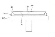
図1は、第1の実施の形態における基板処理装置としてのMMT装置の概略断面図である。このMMT装置は、先に説明した図8と基本的構成は同じであり、異なる点は、ウェハ200とサセプタ217との間に基板載置体10が介設されている点である。従って、図1において、先に説明した図8と同じ機能を有する部分には、同一符号を付して詳細な説明を省略する。
MMT装置は、プラズマ生成領域224で生成されたプラズマによりウェハ200を処理する処理容器203を備える。処理容器203の外側には筒状電極215が配置される。処理容器203の中には、ウェハ200を保持するためのサセプタ217が設けられる。サセプタ217は昇降可能に設けられている。このサセプタ217には、サセプタ217を介してウェハ200を加熱するためのヒータ線21が内蔵されている。また、サセプタ217には、高密度プラズマを生成して、ウェハ200上へプラズマ化した反応ガス20を引き込むためのアース電極22が内蔵されている。このアース電極22は、図示しない高周波整合器を介して接地される。サセプタ217の表面には、ウェハ200とサセプタ217との間に介設されて、ウェハ200を支持する支持部11を有する基板載置体10が搭載される。基板載置体10は非金属材料ないし絶縁体(誘電体)で形成されている。
[First Embodiment]
In the first embodiment, since the electrostatic force is inversely proportional to the square of the distance, the number of particles attached to the back surface of the
FIG. 1 is a schematic cross-sectional view of an MMT apparatus as a substrate processing apparatus in the first embodiment. The basic configuration of this MMT apparatus is the same as that of FIG. 8 described above, and the difference is that the
The MMT apparatus includes a
この基板載置体10は、例えば円板12で構成することができる。円板12は、その表面にウェハ200を支持する支持部11を有して、ウェハ200を支持するようになっている。図示例では、円板12は表裏面がフラットになっており、そのフラットな表面の中央部分がウェハ200の裏面を支持する支持部11となっている。ウェハ200はこの支持部11によって裏面全面が支持されるようになっている。また、円板12のフラットな裏面がサセプタ217の表面と全面接触している。円板12は、例えば石英やセラミックで形成されている。この円板12が、ウェハ200とサセプタ217との間に介在して、ウェハ200とアース電極22との間に一定の距離を確保している。
The
上述したようにMMT装置では、サセプタ217にヒータ線21のみならず、アース電極22も内蔵されているため、ヒータ線21のみを内蔵する熱CVD装置等と異なり、アース電極22によりサセプタ217が帯電するので、この帯電による静電力によりサセプタ217にウェハ200が静電吸着される。また、ウェハ200も帯電するため、この帯電による静電力によりウェハ200にパーティクルが吸着されることになり、ウェハ200へのパーティクル(異物)の吸着が多い。これはプラズマ生成過程でサセプタ217がウェハ200を吸着する状態になり、パーティクルも吸着しやすくなからである。
As described above, since the MMT apparatus incorporates not only the
そこで、上述したように第1の実施の形態は、サセプタ217の表面に基板載置体10を搭載して、ウェハ200とアース電極22との間に、従来よりも大きな一定の距離を設けるようにしている。一定の距離とは、ウェハ200の温度低下を大幅にもたらさない範囲で、ウェハ200へのパーティクル付着を防止できる程度に十分低い静電力となるような距離である。
Therefore, as described above, in the first embodiment, the
このように第1の実施の形態によれば、ウェハ200とアース電極22との間に一定の距離が設けられるので、サセプタ電極(アース電極)によるパーティクルのウェハ200への吸着を確実に抑制することができる。すなわち、ウェハ200とサセプタ217と間に円板12の板厚が加わるので、ウェハ200とサセプタ217間の静電力の低減を実現でき、ウェハ200へのパーティクルの吸着を確実に防止することができる。その結果、ウェハ200に付着するパーティクル数、特にウェハ200の裏面に吸着するパーティクル数の増加を抑え、MMT装置の基板処理能力を向上させることできる。また、ウェハ200上に形成する半導体素子の微細化を実現できる。さらに高い歩留まりを実現することができる。
As described above, according to the first embodiment, since a certain distance is provided between the
ところで、上記基板載置体10は、サセプタ217とは別体に形成するのではなく、サセプタ217の表面を加工して、基板載置体10をサセプタ217と一体に形成することも可能である。しかし、第1の実施の形態のように、基板載置体10をサセプタ217とは別体に形成し、サセプタ217上に基板載置体10を搭載して用いるようにすると、既存のサセプタ217を加工することなくそのまま使用できる。
By the way, the
また、サセプタ217は、石英やセラミックで形成されるが、本実施の形態では石英を用いた。石英の加工には、レーザ加工やダイヤモンドによる切削加工が採用されるが、石英は加工がしづらい。また、石英はガラスであるため、既製品を加工すると割れてしまう可能性もある。また、石英の加工には時間と費用がかかる。このためサセプタ217に直接加工を施す場合と比較して、基板載置体10に加工を施す本実施の形態の方が加工が容易になる。
The
また、基板載置体10としての円板12をサセプタ217とは別体の部品とすることにより、部品(サセプタ、基板載置体)単位で交換が可能となるので、メンテナンスの手間や費用を削減できる。
In addition, since the
[第2の実施の形態]
ところで、上述した第1の実施の形態では、ウェハ200の裏面全面を支持しているが、本発明の一態様によれば、少なくともウェハ200の周縁部を支持すればよい。図2は、そのようなウェハ200の周縁部を支持するようにした第2の実施の形態を示す。本実施の形態は、セプタ217とウェハ200との接触面積が少ないほど、ウェハ200裏面へのパーティクルの付着数を減少させることが可能であるとの知見に基づいてなされている。
[Second Embodiment]
In the first embodiment described above, the entire back surface of the
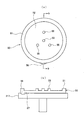
図2に示すように、基板載置体としての円板30は、その表面周縁部にウェハ200の裏面周縁部と接触してウェハ200を支持する凸部31と、ウェハ200の裏面中央部と非接触でウェハ200中央部との間に空間33を形成する凹部32とを有する。
As shown in FIG. 2, the
円板30とウェハ200をできるだけ接触させないように、凸部31はウェハ200のエッジから僅かに内側に入った領域のみで接触するようにする。凸部31によるウェハ200との接触面積は、ウェハ200を十分に支持することが可能な最少の面積とするのが好ましい。この凸部31は、環状の連続した突起で構成されていてもよいし、複数の凹凸が交互に環状に並んだうちの凸部で構成されていてもよい。円板30に設ける凹部32は、凸部31以外の残りの部分全面に設ける。凹部32の深さは、サセプタ217と非接触によりウェハ温度が大幅に降下しない程度であって、静電力を低減するに十分な深さとする。
In order not to make the
第2の実施の形態によれば、円板30の周縁部に設けた凸部31だけでウェハ200を接触させるようにして、第1の実施の形態よりもウェハ200との接触面積の低減を図ったので、円板30へのウェハ200の接触吸着をより確実に抑えることができる。また、円板30に凹部32を設けて、ウェハ200とこれを載置する円板30との間に、円板30の材料よりも誘電率が低い空間33を介在させるようにしたので、ウェハ200とサセプタ217との間に生じる静電力をより確実に低減することができる。その結果、パーティクルのウェハ200裏面への付着をより確実に低減できる。
According to the second embodiment, the contact area with the
また、本実施の形態では、特に円板30に凸部及び凹部加工を施すようにしているが、円板30はサセプタ217とは別体であるので、円板30の加工が一層容易になり、メンテナンスの手間や費用を一層削減できる。
Further, in the present embodiment, the convex portion and the concave portion are processed in particular on the
なお、第2の実施の形態の変形例として、円板30の上下を逆にして凹部32を下側に向け、円板30のフラット面でウェハ200の裏面を全面で支持するようにしてもよい。これによれば、第2の実施の形態よりもパーティクル吸着効果は低減するものの、空間33がアース電極とウェハ200との間に介在するので、第1の実施の形態よりはパーティクル吸着効果が向上する。
As a modification of the second embodiment, the
[第3の実施の形態]
第3の実施の形態は、ウェハ200の周縁部を支持するようにした第2の実施の形態に加えて、図3に示すように、ウェハ200の中央部の一部を支持する第2の支持部として突起45を円板40に設けたものである。ウェハ200の中央部の一部としては、例えば、ウェハ中心部、及びその周辺に少なくとも3箇所以上、合計4箇所以上とすることが好ましい。突起45の高さは凸部41と同じ高さとする。
[Third Embodiment]
In the third embodiment, in addition to the second embodiment in which the peripheral portion of the
このように第3の実施の形態によれば、ウェハ200とサセプタ217の間に、ウェハ周縁部を支持する凸部41、及びウェハ200の中央部を支持する突起45を設けたので、ウェハ200が大型化した場合にウェハ200にたわみが発生しても、ウェハ200の中央部の一部が複数の突起45に支持されるので、ウェハ200のたわみを防止できる。また、ウェハ200とアース電極との間に一定の空間距離を設けることにより、プラズマ処理時にウェハ200へ吸着されるパーティクルを確実に低減することができる。
As described above, according to the third embodiment, the
[第4の実施の形態]
第4の実施の形態は、第3の実施の形態において、図4に示すように、さらに基板載置体としての円板50の裏面にサセプタ固定手段としての凸状の係止部56を設け、これに対応してサセプタ217の表面に、凸状の係止部56と係合する凹状の被係止部57を設けたものである。本実施の形態では、円板50をサセプタ217上へ搭載する時に、サセプタ217の被係止部57に円板50の係止部56を係止する。
[Fourth Embodiment]
In the fourth embodiment, in the third embodiment, as shown in FIG. 4, a
円板50は、通常は、サセプタ217に単に搭載するだけである。サセプタ217は前述したようにウェハ処理時に上昇し、ウェハ処理後は下降する。このとき、例えば、ウェハ200がサセプタ217上に搬送された後、ウェハ処理位置までサセプタ217が上昇移動するときに、その移動に伴って円板50がサセプタ217の表面に沿ってすべり回転し、サセプタ217の中心からウェハ200がずれてしまうことがある。
本実施の形態では、サセプタ217の被係止部57に円板50の係止部56が係止されているので、円板50の回転ずれを有効に防止することができる。なお、凸状係止部、凹状被係止部を設ける場合、円板側を凹状被係止部、サセプタ側を凸状係止部としてもよいが、本実施の形態のように、円板側を凸状係止部、サセプタ側を凹状被係止部にする方が、サセプタ217からウェハ200への熱伝導性の均一化がはかれるので好ましい。
The
In the present embodiment, since the locking
[実施例1]
基板処理装置を構成する基板載置体として、図3に示した構成の円板40を用いた。シリコンウェハの直径は12インチ=300mmである。
円板40の板厚は0.7〜1.5mmである。円板40の板厚は0.7mm〜1.5mmであれば、静電力が十分に低くなり、割れにくくなり加工性も向上し、ウェハ温度の低下も少ない。0.7mm未満だと加工性が難しい。また、持ち運ぶときに割れ易いのでメンテナンスも難しい。1.5mmを超えると加熱源となるサセプタ217とウェハ200との距離が大きくなるため、ウェハ温度が大きく低下するため好ましくない。
円板40は、ウェハ200の直径より約10%大きい形状とした。これはサセプタ217に設けたウェハ200を収納する凹溝となるウェハポケットの大きさと整合させるためである。
[Example 1]
A
The thickness of the
The
パーティクルを低減するために、円板40とウェハ200をできるだけ接触させないように、ウェハ200のエッジから内側に3mmは接するように、円板40の周縁部に3mm幅の凸部を環状突起で形成した。円板の残りの中央部には、0.3mmまたは0.5mmの深さの凹部を設けた。
実施例1では、直径12インチウェハの中心でたわみ量が最大となるため、そのたわみが起こらないようにする必要があったので、円板40の中心に1点の突起と、円周上に3点の突起を設けた。なお、突起の高さは、凹部の深さと同じ0.3mmまたは0.5mmとした。
In order to reduce particles, a convex portion having a width of 3 mm is formed on the peripheral portion of the
In Example 1, since the amount of deflection becomes maximum at the center of the wafer having a diameter of 12 inches, it was necessary to prevent the deflection from occurring. Therefore, one protrusion at the center of the
ウェハと円板は接触するため、アルカリ金属やアルカリ土類金属等の汚染元素がウェハに付着する可能性が高いため、実施例1の円板材料を不純物の少ない合成石英とした。また、ウェハが、そのエッジから内部へ3mm程度は円板と接触するため、円板の接触面を滑らかにし、摩擦による抵抗を少なくした。接触抵抗によりウェハ又は円板が削れてパーティクルが発生するのを防止するためである。 Since the wafer and the disk are in contact with each other, there is a high possibility that contaminating elements such as alkali metals and alkaline earth metals will adhere to the wafer. Therefore, the disk material of Example 1 was made of synthetic quartz with few impurities. Further, since the wafer is in contact with the disk by about 3 mm from the edge to the inside, the contact surface of the disk is made smooth and resistance by friction is reduced. This is to prevent particles from being generated by scraping the wafer or disk due to contact resistance.
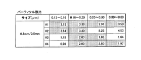
図5に、実施例1の基板処理装置を用いて、円板の凹部深さ0.5mm、凹部深さ0.3mmとしたときの、ウェハ処理後のウェハ裏面に吸着したパーティクル数の測定結果を示す。ウェハサンプル数はそれぞれ4個(#1〜#4)である。パーティクルサイズは0.13〜0.16、0.16〜0.20、0.20〜0.30、及び0.30〜0.80の4つのグループに分けた。 FIG. 5 shows the measurement results of the number of particles adsorbed on the back surface of the wafer after wafer processing when the concave portion depth of the disk is 0.5 mm and the concave portion depth is 0.3 mm using the substrate processing apparatus of Example 1. Indicates. The number of wafer samples is 4 (# 1 to # 4), respectively. The particle size was divided into four groups of 0.13-0.16, 0.16-0.20, 0.20-0.30, and 0.30-0.80.
図6に、実施例1の基板処理装置を用いてウェハ処理を行った後、ウェハの裏面に吸着したパーティクル数比の比較結果を示す。このデータは、凹部深さ0.3mmのサンプルのパーティクル数を、凹部深さ0.5mmのサンプルのパーティクル数で割った値である。誤差範囲も考慮して、2.8士1.0倍の値をマークしてある。 FIG. 6 shows a comparison result of the ratio of the number of particles adsorbed on the back surface of the wafer after performing wafer processing using the substrate processing apparatus of Example 1. This data is a value obtained by dividing the number of particles of a sample having a recess depth of 0.3 mm by the number of particles of a sample having a recess depth of 0.5 mm. Considering the error range, the value of 1.0 times 2.8 is marked.
図5及び図6より、ほとんどの測定結果において、パーティクル数は静電力に近い倍率(2.8±1.0倍)となることから、パーティクル数は静電力に比例することがわかる。また、凹部の深さが深いほど、パーティクル付着の低減効果があることがわかった。 5 and 6, in most measurement results, the number of particles is a magnification close to the electrostatic force (2.8 ± 1.0 times), so that the number of particles is proportional to the electrostatic force. It was also found that the deeper the recess, the more effective the particle adhesion reduction.
上述した測定結果は、次のように理論面からも裏付けられる。
図9に示すように、式F=9×10⁹×Q1Q2/r2[N]より、二つの点電荷Q1とQ2に働く静電力Fは、両電荷Q1とQ2の積に比例し、距離rの二乗に反比例する。
この法則を実施例1に適用するために、
(1)静電力Fを、基板が円板に張り付く力とする、
(2)両電荷Q1とQ2を、基板の電荷Q1と円板の電荷Q2とする、
(3)距離rを、基板Q1と円板Q2間の距離とする、
(4)基板電荷Q1と円板電荷Q2を、上記距離が変わっても同じであるとする、
と仮定する。
そして、上記距離rが0.3mm、0.5mmのときの静電力を上記式からそれぞれ求めると、
F0.3=1/0.32×U
F0.5=1/0.52×U
ここで、U=9×10⁹×Q1Q2/(10-3)2
となる。
2つの距離に応じた静電力の比較をすると、
F0.3/F0.5=(1/0.32×U)/(1/0.52×U)
=2.8倍
が得られる。これより距離0.3mmのときの静電力の方が0.5mmよりも2.8倍大きいことがわかる。
The above measurement results are supported from the theoretical viewpoint as follows.
As shown in FIG. 9, from the formula F = 9 × 10 9 × Q1Q2 / r 2 [N], the electrostatic force F acting on the two point charges Q1 and Q2 is proportional to the product of both charges Q1 and Q2, and the distance It is inversely proportional to the square of r.
In order to apply this law to Example 1,
(1) The electrostatic force F is a force that the substrate sticks to the disk.
(2) Both charges Q1 and Q2 are set as substrate charge Q1 and disk charge Q2.
(3) The distance r is the distance between the substrate Q1 and the disk Q2.
(4) It is assumed that the substrate charge Q1 and the disk charge Q2 are the same even if the distance is changed.
Assume that
Then, when the electrostatic force when the distance r is 0.3 mm and 0.5 mm is obtained from the above equations,
F0.3 = 1 / 0.3 2 × U
F0.5 = 1 / 0.5 2 × U
Here, U = 9 × 10 9 × Q 1 Q 2 / (10 −3 ) 2
It becomes.
When comparing the electrostatic force according to the two distances,
F0.3 / F0.5 = (1 / 0.3 2 × U) / (1 / 0.5 2 × U)
= 2.8 times is obtained. This shows that the electrostatic force when the distance is 0.3 mm is 2.8 times larger than 0.5 mm.
実施例1の基板処理装置では、ウェハとサセプタの間に円板を挟んでいるため、基板温度が6%減少するという結果が出たものの、従来よりもウェハ裏面付着のパーティクルを5000個から250個に低減することができ、低減率が95%にも達した。 In the substrate processing apparatus according to the first embodiment, since the disk is sandwiched between the wafer and the susceptor, the substrate temperature is reduced by 6%. The reduction rate reached 95%.
[比較例1]
図7に示すように、ウェハ200を保持する保持手段として、基板載置体は用いずにサセプタ217のみを用いた。サセプタ217に基板載置体を設置すると、サセプタ217からウェハ200への熱伝導が悪くなる。このため、サセプタ217のウェハ200と接触する表面に、実施例1における凹部や凸部を直接加工した。これによれば、サセプタと基板載置体とが一体になるので、部品(基板載置体、サセプタ)単位での交換ができず、メンテナンスが困難であった。また、加工も困難であった。
[Comparative Example 1]
As shown in FIG. 7, only the
以下に本発明の好ましい態様を付記する。
本発明の第1の態様は、プラズマにより基板を処理する処理容器と、前記処理容器の中に設けられ、アース電極を有するサセプタと、少なくとも基板の周縁部を支持する支持部を有し、前記サセプタ上に設けられる基板載置体とを設けた基板処理装置である。
基板とアース電極との間に基板載置体が設けられるので、プラズマ処理時に基板へ吸着されるパーティクルを低減できる。
Hereinafter, preferred embodiments of the present invention will be additionally described.
According to a first aspect of the present invention, there is provided a processing container for processing a substrate by plasma, a susceptor provided in the processing container and having a ground electrode, and a support part for supporting at least a peripheral part of the substrate, A substrate processing apparatus provided with a substrate mounting body provided on a susceptor.
Since the substrate mounting body is provided between the substrate and the ground electrode, particles adsorbed to the substrate during the plasma processing can be reduced.
本発明の第2の態様は、第1の態様において、前記基板載置体の前記支持部は凸状である基板処理装置である。
サセプタに設けた基板載置体で基板を支持する場合、特にサセプタと基板載置体との接触面積が問題になり、それがパーティクル低減効果に影響するが、本発明によれば凸状の支持部により基板が支持されるので、上記接触面積が低減されてパーティクル低減効果をより向上できる。
A second aspect of the present invention is the substrate processing apparatus according to the first aspect, wherein the support portion of the substrate platform is convex.
When the substrate is supported by the substrate mounting body provided on the susceptor, the contact area between the susceptor and the substrate mounting body becomes a problem, which affects the particle reduction effect. Since the substrate is supported by the portion, the contact area is reduced, and the particle reduction effect can be further improved.
本発明の第3の態様は、第1ないし第2の態様において、前記支持部は、基板周縁部を支持する支持部の他に、基板周縁部以外を支持する第2の支持部を有する基板処理装置である。
基板周縁部以外を支持する第2の支持部を有すると、基板の口径が大きくなっても、第2の支持部により、たわみやすい基板周縁部以外を支持できるため、基板のたわみを防止できる。
According to a third aspect of the present invention, in the first or second aspect, the support portion includes a second support portion that supports a portion other than the substrate peripheral portion in addition to the support portion that supports the substrate peripheral portion. It is a processing device.
When the second support portion that supports the portion other than the peripheral portion of the substrate is provided, even if the diameter of the substrate is increased, the second support portion can support the portion other than the peripheral portion of the substrate that is easily bent, so that the substrate can be prevented from being bent.
本発明の第4の態様は、第1ないし第3の態様において、前記基板載置体とサセプタとが、サセプタ上の基板載置体のすべり回転を阻止する固定手段により係合されている基板処理装置である。これによれば、サセプタが昇降してもサセプタ上の基板載置体の回転を抑えることができる。 According to a fourth aspect of the present invention, in the first to third aspects, the substrate mounting body and the susceptor are engaged with each other by a fixing unit that prevents sliding rotation of the substrate mounting body on the susceptor. It is a processing device. According to this, even if a susceptor raises / lowers, rotation of the substrate mounting body on a susceptor can be suppressed.
本発明の第5の態様は、第1ないし第4の態様において、前記基板載置体が石英で形成されている基板処理装置である。これによれば、石英製の基板載置体がサセプタと別体に構成されているため、基板載置体の加工、メンテナンス等が容易になる。 A fifth aspect of the present invention is the substrate processing apparatus according to any one of the first to fourth aspects, wherein the substrate mounting body is made of quartz. According to this, since the quartz substrate mounting body is configured separately from the susceptor, processing, maintenance, and the like of the substrate mounting body are facilitated.
10 基板載置体
11 支持部
22 アース電極
200 ウェハ(基板)
203 処理容器
217 サセプタ
224 プラズマ生成領域
DESCRIPTION OF
203
Claims (3)
前記処理容器の中に設けられたアース電極を有するサセプタと、
前記サセプタの上に環状に設けられ、前記基板の端部を内縁側で支持し、外縁の直径が当該基板の直径よりも大きく構成された凸状支持部、及び前記基板を載置した際、前記基板の裏面中央部との間に空間を形成する凹部を有する基板載置体と、
を備えた基板処理装置。 A processing vessel for processing a substrate with plasma;
A susceptor having a ground electrode provided in the processing vessel;
The provided annularly on the susceptor, support the ends of the substrate at the inner edge, a convex support portion diameter of the outer edge is configured larger than the diameter of the substrate, and upon mounting the substrate, A substrate mounting body having a recess that forms a space between the substrate and the center of the back surface of the substrate;
A substrate processing apparatus comprising:
前記処理容器の中に設けられアース電極を有するサセプタと、
前記サセプタの上に環状に設けられ、前記基板の端部を内縁側で支持し、外縁の直径が当該基板の直径よりも大きく構成された凸状支持部、及び前記基板を載置した際、前記基板の裏面中央部との間に空間を形成する凹部を有する基板載置体と、
を備えた基板処理装置を用いた半導体装置の製造方法であって、
基板が前記基板載置体の凸状支持部上に載置される工程と、
前記載置された基板を処理する工程と、
を有する半導体装置の製造方法。 A processing vessel for processing a substrate with plasma;
A susceptor provided in the processing vessel and having a ground electrode;
The provided annularly on the susceptor, support the ends of the substrate at the inner edge, a convex support portion diameter of the outer edge is configured larger than the diameter of the substrate, and upon mounting the substrate, A substrate mounting body having a recess that forms a space between the substrate and the center of the back surface of the substrate;
A method for manufacturing a semiconductor device using a substrate processing apparatus comprising:
A step of placing a substrate on the convex support portion of the substrate placement body;
Processing the previously placed substrate; and
A method for manufacturing a semiconductor device comprising:
Priority Applications (1)
| Application Number | Priority Date | Filing Date | Title |
|---|---|---|---|
| JP2006216028A JP4961179B2 (en) | 2006-08-08 | 2006-08-08 | Substrate processing apparatus and semiconductor device manufacturing method |
Applications Claiming Priority (1)
| Application Number | Priority Date | Filing Date | Title |
|---|---|---|---|
| JP2006216028A JP4961179B2 (en) | 2006-08-08 | 2006-08-08 | Substrate processing apparatus and semiconductor device manufacturing method |
Publications (3)
| Publication Number | Publication Date |
|---|---|
| JP2008042023A JP2008042023A (en) | 2008-02-21 |
| JP2008042023A5 JP2008042023A5 (en) | 2009-09-10 |
| JP4961179B2 true JP4961179B2 (en) | 2012-06-27 |
Family
ID=39176685
Family Applications (1)
| Application Number | Title | Priority Date | Filing Date |
|---|---|---|---|
| JP2006216028A Active JP4961179B2 (en) | 2006-08-08 | 2006-08-08 | Substrate processing apparatus and semiconductor device manufacturing method |
Country Status (1)
| Country | Link |
|---|---|
| JP (1) | JP4961179B2 (en) |
Families Citing this family (6)
| Publication number | Priority date | Publication date | Assignee | Title |
|---|---|---|---|---|
| JP2010084230A (en) * | 2008-09-04 | 2010-04-15 | Tokyo Electron Ltd | Film deposition apparatus, substrate process apparatus, and turntable |
| JP5264403B2 (en) * | 2008-10-14 | 2013-08-14 | 株式会社アルバック | Substrate tray, etching apparatus and etching method used in plasma etching apparatus |
| JP5869899B2 (en) | 2011-04-01 | 2016-02-24 | 株式会社日立国際電気 | Substrate processing apparatus, semiconductor device manufacturing method, substrate processing method, and susceptor cover |
| JP6066571B2 (en) * | 2012-02-17 | 2017-01-25 | 株式会社日立国際電気 | Substrate processing apparatus and semiconductor device manufacturing method |
| JP2018095916A (en) * | 2016-12-13 | 2018-06-21 | 株式会社日立国際電気 | Substrate treatment apparatus, lithography temperature manufacturing method, program |
| JP2020021922A (en) * | 2018-07-24 | 2020-02-06 | 住友電気工業株式会社 | Substrate heating unit and surface plate |
Family Cites Families (8)
| Publication number | Priority date | Publication date | Assignee | Title |
|---|---|---|---|---|
| JP3064409B2 (en) * | 1990-11-30 | 2000-07-12 | 株式会社日立製作所 | Holding device and semiconductor manufacturing apparatus using the same |
| JPH06349810A (en) * | 1993-06-02 | 1994-12-22 | Hitachi Electron Eng Co Ltd | Vapor phase reaction apparatus |
| JP3312163B2 (en) * | 1994-11-18 | 2002-08-05 | 日本電信電話株式会社 | Vacuum suction device |
| JP2002134487A (en) * | 2000-10-25 | 2002-05-10 | Hitachi Ltd | Method for manufacturing semiconductor device |
| JP2003142566A (en) * | 2001-11-07 | 2003-05-16 | New Creation Co Ltd | Vacuum sucker and its manufacturing method |
| JP2005064284A (en) * | 2003-08-14 | 2005-03-10 | Asm Japan Kk | Semiconductor substrate holding device |
| JP4444843B2 (en) * | 2005-01-31 | 2010-03-31 | 住友大阪セメント株式会社 | Electrostatic chuck |
| JP2007067394A (en) * | 2005-08-05 | 2007-03-15 | Tokyo Electron Ltd | Substrate processing apparatus and substrate stage used for the same |
-
2006
- 2006-08-08 JP JP2006216028A patent/JP4961179B2/en active Active
Also Published As
| Publication number | Publication date |
|---|---|
| JP2008042023A (en) | 2008-02-21 |
Similar Documents
| Publication | Publication Date | Title |
|---|---|---|
| CN112992639A (en) | Substrate processing apparatus having electrostatic chuck and substrate processing method | |
| US8592712B2 (en) | Mounting table structure and plasma film forming apparatus | |
| US7837828B2 (en) | Substrate supporting structure for semiconductor processing, and plasma processing device | |
| KR101924488B1 (en) | Confined process volume pecvd chamber | |
| KR102487342B1 (en) | Electrostatic chuck and a plasma apparatus for processing substrates having the same | |
| CN106992107A (en) | System and method of the frequency modulation(PFM) radio-frequency power supply to control plasma instability | |
| KR102092623B1 (en) | Plasma processing apparatus | |
| JP4777790B2 (en) | Structure for plasma processing chamber, plasma processing chamber, and plasma processing apparatus | |
| JP2009177199A (en) | Plasma processing device and focus ring | |
| KR102353796B1 (en) | Electrostatic chuck, placing table, plasma processing apparatus, and method of manufacturing electrostatic chuck | |
| JP4961179B2 (en) | Substrate processing apparatus and semiconductor device manufacturing method | |
| TWI717631B (en) | Plasma processing device | |
| KR102432857B1 (en) | plasma processing apparatus and manufacturing method of semiconductor device using the same | |
| JP2007250860A (en) | Plasma processor and electrode assembly therefor | |
| TW202130226A (en) | Stage and plasma processing apparatus | |
| CN111172515A (en) | Cleaning method and film forming method | |
| US8034213B2 (en) | Plasma processing apparatus and plasma processing method | |
| JP7382329B2 (en) | Process kit for substrate supports | |
| CN116457931A (en) | High-temperature bipolar electrostatic chuck | |
| TW201543532A (en) | Method and device for plasma treatment of substrates | |
| TW202117912A (en) | Substrate support and plasma processing apparatus | |
| JP7110020B2 (en) | Substrate support device and plasma processing device | |
| JP2008053489A (en) | Substrate processing apparatus | |
| JP5171584B2 (en) | Substrate mounting table for substrate processing apparatus, substrate processing apparatus, and method for manufacturing semiconductor device | |
| US20210027994A1 (en) | Shutter mechanism and substrate processing apparatus |
Legal Events
| Date | Code | Title | Description |
|---|---|---|---|
| A521 | Request for written amendment filed |
Free format text: JAPANESE INTERMEDIATE CODE: A523 Effective date: 20090728 |
|
| A621 | Written request for application examination |
Free format text: JAPANESE INTERMEDIATE CODE: A621 Effective date: 20090728 |
|
| A977 | Report on retrieval |
Free format text: JAPANESE INTERMEDIATE CODE: A971007 Effective date: 20100820 |
|
| A131 | Notification of reasons for refusal |
Free format text: JAPANESE INTERMEDIATE CODE: A131 Effective date: 20110531 |
|
| A521 | Request for written amendment filed |
Free format text: JAPANESE INTERMEDIATE CODE: A523 Effective date: 20110725 |
|
| A131 | Notification of reasons for refusal |
Free format text: JAPANESE INTERMEDIATE CODE: A131 Effective date: 20111220 |
|
| RD03 | Notification of appointment of power of attorney |
Free format text: JAPANESE INTERMEDIATE CODE: A7423 Effective date: 20120213 |
|
| A521 | Request for written amendment filed |
Free format text: JAPANESE INTERMEDIATE CODE: A523 Effective date: 20120216 |
|
| TRDD | Decision of grant or rejection written | ||
| A01 | Written decision to grant a patent or to grant a registration (utility model) |
Free format text: JAPANESE INTERMEDIATE CODE: A01 Effective date: 20120313 |
|
| A01 | Written decision to grant a patent or to grant a registration (utility model) |
Free format text: JAPANESE INTERMEDIATE CODE: A01 |
|
| A61 | First payment of annual fees (during grant procedure) |
Free format text: JAPANESE INTERMEDIATE CODE: A61 Effective date: 20120326 |
|
| FPAY | Renewal fee payment (event date is renewal date of database) |
Free format text: PAYMENT UNTIL: 20150330 Year of fee payment: 3 |
|
| R150 | Certificate of patent or registration of utility model |
Ref document number: 4961179 Country of ref document: JP Free format text: JAPANESE INTERMEDIATE CODE: R150 Free format text: JAPANESE INTERMEDIATE CODE: R150 |
|
| R250 | Receipt of annual fees |
Free format text: JAPANESE INTERMEDIATE CODE: R250 |
|
| R250 | Receipt of annual fees |
Free format text: JAPANESE INTERMEDIATE CODE: R250 |
|
| R250 | Receipt of annual fees |
Free format text: JAPANESE INTERMEDIATE CODE: R250 |
|
| R250 | Receipt of annual fees |
Free format text: JAPANESE INTERMEDIATE CODE: R250 |
|
| S111 | Request for change of ownership or part of ownership |
Free format text: JAPANESE INTERMEDIATE CODE: R313111 |
|
| S531 | Written request for registration of change of domicile |
Free format text: JAPANESE INTERMEDIATE CODE: R313531 |
|
| R350 | Written notification of registration of transfer |
Free format text: JAPANESE INTERMEDIATE CODE: R350 |
|
| R250 | Receipt of annual fees |
Free format text: JAPANESE INTERMEDIATE CODE: R250 |
|
| R250 | Receipt of annual fees |
Free format text: JAPANESE INTERMEDIATE CODE: R250 |
|
| R250 | Receipt of annual fees |
Free format text: JAPANESE INTERMEDIATE CODE: R250 |
|
| R250 | Receipt of annual fees |
Free format text: JAPANESE INTERMEDIATE CODE: R250 |
|
| R250 | Receipt of annual fees |
Free format text: JAPANESE INTERMEDIATE CODE: R250 |
|
| R250 | Receipt of annual fees |
Free format text: JAPANESE INTERMEDIATE CODE: R250 |