JP4957925B2 - Amplification type solid-state imaging device - Google Patents
Amplification type solid-state imaging device Download PDFInfo
- Publication number
- JP4957925B2 JP4957925B2 JP2009019218A JP2009019218A JP4957925B2 JP 4957925 B2 JP4957925 B2 JP 4957925B2 JP 2009019218 A JP2009019218 A JP 2009019218A JP 2009019218 A JP2009019218 A JP 2009019218A JP 4957925 B2 JP4957925 B2 JP 4957925B2
- Authority
- JP
- Japan
- Prior art keywords
- transistor
- capacitor
- amplification
- imaging device
- pixel
- Prior art date
- Legal status (The legal status is an assumption and is not a legal conclusion. Google has not performed a legal analysis and makes no representation as to the accuracy of the status listed.)
- Expired - Fee Related
Links
- 230000003321 amplification Effects 0.000 title claims description 162
- 238000003199 nucleic acid amplification method Methods 0.000 title claims description 162
- 238000003384 imaging method Methods 0.000 title claims description 49
- 239000003990 capacitor Substances 0.000 claims description 86
- 230000015654 memory Effects 0.000 claims description 66
- 238000006243 chemical reaction Methods 0.000 claims description 9
- 239000011159 matrix material Substances 0.000 claims description 9
- 238000000034 method Methods 0.000 claims description 7
- 238000010586 diagram Methods 0.000 description 14
- 230000008859 change Effects 0.000 description 10
- 230000000875 corresponding effect Effects 0.000 description 6
- 230000004044 response Effects 0.000 description 5
- 230000001276 controlling effect Effects 0.000 description 4
- 238000005070 sampling Methods 0.000 description 4
- 230000006870 function Effects 0.000 description 3
- 230000002596 correlated effect Effects 0.000 description 2
- 230000007423 decrease Effects 0.000 description 2
- 238000009825 accumulation Methods 0.000 description 1
- 230000008901 benefit Effects 0.000 description 1
- 230000000295 complement effect Effects 0.000 description 1
- 230000000694 effects Effects 0.000 description 1
- 238000007687 exposure technique Methods 0.000 description 1
- 230000006872 improvement Effects 0.000 description 1
- 229910044991 metal oxide Inorganic materials 0.000 description 1
- 150000004706 metal oxides Chemical class 0.000 description 1
- 230000002093 peripheral effect Effects 0.000 description 1
- 230000009467 reduction Effects 0.000 description 1
- 239000004065 semiconductor Substances 0.000 description 1
- 238000004088 simulation Methods 0.000 description 1
- 230000001052 transient effect Effects 0.000 description 1
- 230000007704 transition Effects 0.000 description 1
Images


Description
本発明は、画素内にメモリを有する増幅型固体撮像装置に関する。 The present invention relates to an amplification type solid-state imaging device having a memory in a pixel.
一般に、増幅型固体撮像装置としては、増幅機能を持たせた画素部とその画素部の周辺に配置された走査回路とを有し、該走査回路によって前記画素部から画素データを読み出すものが普及している。
このような増幅型固体撮像装置の一例としては、画素部が周辺の駆動回路及び信号処理回路と一体化するのに有利なCMOS(コンプリメンタリ・メタル・オキサイド・セミコンダクタ)によって構成されたAPS(Active Pixel Sensor)型イメージセンサが知られている。このようなAPS型イメージセンサの中でも、近年は高画質が得られる4トランジスタ型が主流になりつつある。
In general, an amplification type solid-state imaging device has a pixel unit having an amplification function and a scanning circuit arranged around the pixel unit, and reads out pixel data from the pixel unit by the scanning circuit. is doing.
As an example of such an amplification-type solid-state imaging device, an APS (Active Pixel) configured by a CMOS (Complementary Metal Oxide Semiconductor), which is advantageous for integrating a pixel portion with a peripheral driving circuit and a signal processing circuit. Sensor) type image sensors are known. Among such APS type image sensors, a 4-transistor type capable of obtaining high image quality is becoming mainstream in recent years.
図16は、画素100内に4つのNMOSトランジスタを備えた、従来の4トランジスタ型の画素構成例を示した回路図である。
図16では、受光素子PDは通常埋め込みフォトダイオードで構成され、受光素子PDから接続部FDへは転送トランジスタTXによって信号電荷が転送される。接続部FDは、受光素子PDから信号電荷が転送される前に、リセットトランジスタRTによってリセットトランジスタRTのドレイン電圧である電源電圧Vddにリセットされる。次に、転送トランジスタTXがオンして、受光素子PDからの信号電荷が接続部FDに転送される。前記リセット後及び前記信号電荷転送後の接続部FDの電圧は、増幅トランジスタSFによって増幅され、選択トランジスタSLを介して読み出し信号線Vsigへ読み出される。読み出し信号線Vsigの一端には定電流負荷トランジスタCLが接続され、定電流負荷トランジスタCLのドレインから出力電圧Voが得られる。
FIG. 16 is a circuit diagram showing an example of a conventional four-transistor pixel configuration in which four NMOS transistors are provided in the
In FIG. 16, the light receiving element PD is normally formed of a buried photodiode, and signal charges are transferred from the light receiving element PD to the connection portion FD by the transfer transistor TX. The connection unit FD is reset to the power supply voltage Vdd that is the drain voltage of the reset transistor RT by the reset transistor RT before the signal charge is transferred from the light receiving element PD. Next, the transfer transistor TX is turned on, and the signal charge from the light receiving element PD is transferred to the connection portion FD. The voltage of the connection portion FD after the reset and the signal charge transfer is amplified by the amplification transistor SF and read out to the read signal line Vsig through the selection transistor SL. A constant current load transistor CL is connected to one end of the read signal line Vsig, and an output voltage Vo is obtained from the drain of the constant current load transistor CL.
図17は、図16の画素100をマトリクス状に配置した画素アレイ200を含む増幅型固体撮像装置をなす2次元イメージセンサの構成例を示した図である。
図17において、11はリセットトランジスタRT及び増幅トランジスタSFの各ドレインに電源電圧Vddをそれぞれ印加するための電源線であり、電源線11は増幅型固体撮像装置全体の電源線13に直接接続されている。また、駆動線16は転送トランジスタ駆動線、リセットトランジスタ駆動線及び選択トランジスタ駆動線を1つにして示したものである。
各画素行では、行デコーダ回路14により特定の行が選択され、行駆動回路15を介して駆動線16へ駆動信号が与えられる。読み出し信号線Vsigからの信号は、コラム信号処理回路17に入力され、コラム信号処理回路17でアナログ又はアナログとデジタルの信号処理が施される。この後、コラムデコーダ回路18によって、コラムごとの信号が水平信号線19へ読み出され、最終的に増幅型固体撮像装置外部に出力される。
FIG. 17 is a diagram illustrating a configuration example of a two-dimensional image sensor constituting an amplification type solid-state imaging device including a
In FIG. 17,
In each pixel row, a specific row is selected by the
図17で示した構成では、各画素は行ごとに順次読み出され、画素100では該読み出しが行われるときまで受光素子PDに蓄積された信号を出力するため、各画素の信号は時間的に行ごとに順次ずれが生じ、動きのある被写体を撮像する場合には、動きに応じて像が歪んでいた。このような問題を解決するために、画素内にメモリを備え、すべての画素を同時に読み出して該メモリに書き込み、その後、該メモリ内の情報を順次読み出すようにした一括露光技術があった。しかし、この場合、受光素子からの信号を前記メモリに書き込んでから読み出すまでの間にノイズが増大し、S/N比が低下するという問題があった。このようなことから、受光素子の信号を増幅してからメモリに書き込む技術があり、図18はこの一例を示した回路図である(例えば、特許文献1参照。)。
In the configuration shown in FIG. 17, each pixel is sequentially read out row by row, and the
図18に示した画素110は、図16で示した画素100に、第1の増幅トランジスタSF1、定電流負荷VB、電流制御スイッチSW、書き込みスイッチWr及びメモリCmを追加した構成になっている。なお、図18では、第2の増幅トランジスタSF2が図16の増幅トランジスタSFに相当しており、電流制御スイッチSWは電源側に設けるようにしてもよい。
例えば、画素110を使用して図17に示した2次元イメージセンサを構成し、まず、すべての画素を一括動作させて、受光素子PDからの信号をメモリCmに書き込むようにする。即ち、電流制御スイッチSWをオンさせた後、書き込みスイッチWrをオンさせ、第1の増幅トランジスタSF1によって増幅された受光素子PDからの信号をメモリCmに書き込む。
A
For example, the
この後、書き込みスイッチWrをオフさせ、次に電流制御スイッチSWをオフさせて一括書き込み動作が終了する。読み出し動作は、行ごとに順次行われる。すなわち、メモリCmに保持された信号を、第2の増幅トランジスタSF2及び選択トランジスタSLを介して読み出し信号線Vsigへ読み出す動作を、行ごとに順次行われる。読み出し信号線Vsigの一端には定電流負荷トランジスタCLが接続され、出力電圧Voが行ごとに順次得られる。 Thereafter, the write switch Wr is turned off, and then the current control switch SW is turned off to complete the batch write operation. The read operation is sequentially performed for each row. That is, the operation of reading the signal held in the memory Cm to the read signal line Vsig through the second amplification transistor SF2 and the selection transistor SL is sequentially performed for each row. A constant current load transistor CL is connected to one end of the read signal line Vsig, and the output voltage Vo is sequentially obtained for each row.
しかしながら、図18の構成では下記(a)〜(d)の課題が伴っていた。
(a)すべての画素で第1の増幅トランジスタSF1が同時にオンするため、2次元イメージセンサ素子全体では過大な電流が流れる。例えば、1画素当り1μAとしても100万画素あれば、該素子全体で1Aにもなる。
(b)1画素当りの電流を抑圧するために、定電流負荷VBのゲート電圧をしきい値Vth付近にすると、しきい値Vthのばらつきによって電流値が画素ごとに大きく変動する。
(c)1画素内に定電流負荷VB及び電流制御スイッチSWの2つのトランジスタ、並びに該各トランジスタへの制御信号線が必要になり、画素レイアウトが複雑化する。
However, the configuration shown in FIG. 18 has the following problems (a) to (d).
(A) Since the first amplification transistor SF1 is simultaneously turned on in all the pixels, an excessive current flows in the entire two-dimensional image sensor element. For example, if 1 μA per pixel is 1 million pixels, the entire device is 1 A.
(B) When the gate voltage of the constant current load VB is set near the threshold value Vth in order to suppress the current per pixel, the current value greatly varies from pixel to pixel due to variations in the threshold value Vth.
(C) Two transistors, the constant current load VB and the current control switch SW, and a control signal line to each of the transistors are required in one pixel, and the pixel layout becomes complicated.
(d)第1の増幅トランジスタSF1と定電流負荷VBによって構成されたソースフォロワ回路で発生するノイズは、下記(1)式のように表される。

前記(1)式では、kはボルツマン定数、Tは絶対温度、gm1及びgm2は第1の増幅トランジスタSF1及び定電流負荷VBの相互コンダクタンスをそれぞれ示している。画素領域内では、面積の制約から相互コンダクタンスgm1及びgm2は同程度の値になるため、ノイズ電力は1トランジスタの場合と比較して2倍程度になる。
(D) Noise generated in the source follower circuit constituted by the first amplification transistor SF1 and the constant current load VB is expressed by the following equation (1).
In the equation (1), k is a Boltzmann constant, T is an absolute temperature, and gm1 and gm2 are transconductances of the first amplification transistor SF1 and the constant current load VB, respectively. In the pixel region, the mutual conductances g m1 and g m2 have substantially the same value due to area restrictions, so that the noise power is about twice that in the case of one transistor.
1画素当りの電流を安定して小さくする手法として、図19のような回路が考えられる。すなわち、図19では、定電流負荷VBのソース側に高抵抗RLが挿入され、MOSトランジスタのバックゲート効果によって、ゲート電圧をしきい値Vth以下のサブスレッショルド領域として電流を大幅に抑制しても、ソース電圧を安定して保つことができる。しかし、例えば100万画素で素子全体の電流を100mA以下にするためには、定電流負荷VBのソース電圧を1Vとし、RL=10MΩとする必要があり、このような高抵抗値の抵抗を1画素内に形成するのは困難であった。 As a technique for stably reducing the current per pixel, a circuit as shown in FIG. 19 can be considered. That is, in FIG. 19, even when the high resistance RL is inserted on the source side of the constant current load VB and the gate voltage is made a subthreshold region having a threshold voltage Vth or less due to the back gate effect of the MOS transistor, the current is greatly suppressed. The source voltage can be kept stable. However, for example, in order to reduce the current of the entire element to 100 mA or less in 1 million pixels, it is necessary to set the source voltage of the constant current load VB to 1 V and RL = 10 MΩ. It was difficult to form in a pixel.
更に、図18及び図19で示したような、通常のソースフォロワ出力を容量値Cmのメモリに書き込む場合、ノイズ電力で表すと下記(2)式のようなkTCノイズが発生し、このようなkTCノイズは、前記ソースフォロワノイズに加算され、ノイズの増大を招いていた。
Further, when a normal source follower output as shown in FIGS. 18 and 19 is written into a memory having a capacitance value Cm, kTC noise as shown in the following equation (2) is generated in terms of noise power. The kTC noise is added to the source follower noise, leading to an increase in noise.
本発明は、このような問題を解決するためになされたものであり、簡単な回路構成で、メモリへの書き込み時における電流を抑圧することができ、安定した動作と高い性能を得ることができる増幅型固体撮像装置を得ることを目的とする。 The present invention has been made to solve such a problem. With a simple circuit configuration, the current at the time of writing to the memory can be suppressed, and stable operation and high performance can be obtained. An object is to obtain an amplification type solid-state imaging device.
この発明に係る増幅型固体撮像装置は、内部にメモリを有する単位画素が行列状に複数配置されてなる画素アレイと、該画素アレイを構成する各画素に対する動作制御を行う制御回路部とを備えた増幅型固体撮像装置において、
前記各画素は、
受光した光に応じた信号を生成して出力する光電変換部と、
該光電変換部から出力された信号がゲートに入力され、該ゲートに入力された信号を増幅して出力するMOSトランジスタからなる第1の増幅トランジスタと、
該第1の増幅トランジスタから出力された信号を記憶するための前記メモリをなす第1の容量と、
前記第1の増幅トランジスタから出力された信号に対して、該第1の容量への出力制御を行って該第1の容量への書き込み制御を行う第1の書き込みスイッチ部と、
前記第1の容量に書き込まれた信号がゲートに入力され、該ゲートに入力された信号を増幅して出力するMOSトランジスタからなる第2の増幅トランジスタと、
前記第1の容量に書き込まれた信号を所定の第1電圧に初期化する初期化トランジスタと、
をそれぞれ備え、
前記第1の増幅トランジスタは、前記第1の容量のみを負荷とし、前記第1の書き込みスイッチ部は、前記初期化トランジスタによって前記第1の容量に対する前記初期化が行われた後、所定の期間、前記第1の増幅トランジスタから出力された信号を前記第1の容量へ出力して前記第1の容量への書き込みを行うものである。
An amplification type solid-state imaging device according to the present invention includes a pixel array in which a plurality of unit pixels each having a memory are arranged in a matrix, and a control circuit unit that performs operation control on each pixel constituting the pixel array. In the amplification type solid-state imaging device,
Each pixel is
A photoelectric conversion unit that generates and outputs a signal corresponding to the received light; and
A first amplification transistor composed of a MOS transistor for inputting a signal output from the photoelectric conversion unit to a gate and amplifying and outputting the signal input to the gate;
A first capacitor forming the memory for storing a signal output from the first amplification transistor;
A first write switch unit that performs output control to the first capacitor to control writing to the first capacitor with respect to a signal output from the first amplification transistor;
A second amplifying transistor comprising a MOS transistor for inputting a signal written in the first capacitor to a gate and amplifying and outputting the signal input to the gate;
An initialization transistor for initializing a signal written in the first capacitor to a predetermined first voltage;
Each with
The first amplifying transistor has only the first capacitor as a load, and the first write switch unit has a predetermined period after the initialization with respect to the first capacitor is performed by the initialization transistor. The signal output from the first amplifying transistor is output to the first capacitor and written to the first capacitor.
具体的には、前記第1の書き込みスイッチ部は、前記第1の増幅トランジスタが飽和領域動作からサブスレッショルド領域動作に移行して準安定状態になる期間、前記第1の増幅トランジスタから出力された信号を前記第1の容量へ出力して前記第1の容量への書き込みを行うようにした。 Specifically, the first write switch unit is output from the first amplification transistor during a period in which the first amplification transistor shifts from the saturation region operation to the subthreshold region operation and becomes a metastable state. A signal is output to the first capacitor to perform writing to the first capacitor.
また、前記制御回路部は、前記画素アレイを構成する前記各画素に対して、同時に作動させて該各画素内の前記第1の容量に対する書き込み動作をそれぞれ行わせた後、所定の方法で前記各画素の前記第1の容量からの読み出しを順次行うようにした。 In addition, the control circuit unit operates each of the pixels constituting the pixel array at the same time to perform a writing operation on the first capacitor in each of the pixels, and then performs a predetermined method on the pixels. Reading from the first capacitor of each pixel was sequentially performed.
この場合、前記画素アレイ内の各画素は、列単位で前記第1の増幅トランジスタが電源線に接続され、該電源線は列単位ごとにそれぞれ抵抗を介して所定の電源電圧に接続されるようにした。 In this case, in each pixel in the pixel array, the first amplification transistor is connected to a power supply line in a column unit, and the power supply line is connected to a predetermined power supply voltage through a resistor for each column unit. I made it.
また、前記画素アレイ内の各画素は、列単位で前記第1の増幅トランジスタが電源線に接続され、全列の該各電源線はそれぞれ接続され、該接続部は抵抗を介して電源電圧に接続されるようにしてもよい。 In each pixel in the pixel array, the first amplification transistor is connected to a power supply line in units of columns, the power supply lines in all columns are connected to each other, and the connection portion is connected to a power supply voltage via a resistor. You may make it connect.
また、前記制御回路部は、前記画素アレイから行ごとに順次読み出しを行う際、非選択行の各画素における前記初期化トランジスタに対して、前記第2の増幅トランジスタがそれぞれ不活性になるような前記第1電圧に初期化させるようにした。 Further, when the control circuit section sequentially reads out the row from the pixel array, the second amplification transistor is inactivated with respect to the initialization transistor in each pixel of the non-selected row. The first voltage is initialized.
更に、前記各画素は、
前記第1の増幅トランジスタから出力された信号を記憶するための前記メモリをなす1つ以上の第2の容量と、
前記第1の増幅トランジスタから出力された信号に対して、対応する該第2の容量への出力制御を行って該第2の容量への書き込み制御を行う1つ以上の第2の書き込みスイッチ部と、
前記第1の容量に書き込まれた信号に対して、前記第2の増幅トランジスタのゲートへの出力制御を行う第1の読み出しスイッチ部と、
対応する前記第2の容量に書き込まれた信号に対して、前記第2の増幅トランジスタのゲートへの出力制御を行う1つ以上の第2の読み出しスイッチ部と、
を備え、
前記第1の増幅トランジスタは、前記第1又は第2の容量のみを負荷とし、前記初期化トランジスタは、前記第2の容量に書き込まれた信号を前記所定の第1電圧に初期化し、前記第2の書き込みスイッチ部は、前記初期化トランジスタによって前記第2の容量に対する前記初期化が行われた後、所定の期間、前記第1の増幅トランジスタから出力された信号を前記第2の容量へ出力して前記第2の容量への書き込みを行うようにしてもよい。
Further, each pixel is
One or more second capacitors forming the memory for storing a signal output from the first amplification transistor;
One or more second write switch units for performing output control to the corresponding second capacitor and controlling writing to the second capacitor with respect to the signal output from the first amplification transistor When,
A first read switch unit for controlling output to the gate of the second amplification transistor with respect to a signal written to the first capacitor;
One or more second read switch units for controlling output to the gate of the second amplification transistor with respect to a signal written in the corresponding second capacitor;
With
The first amplification transistor uses only the first or second capacitor as a load, and the initialization transistor initializes a signal written in the second capacitor to the predetermined first voltage, and The second write switch unit outputs a signal output from the first amplification transistor to the second capacitor for a predetermined period after the initialization of the second capacitor is performed by the initialization transistor. Then, writing to the second capacitor may be performed.
この場合、前記第2の書き込みスイッチ部は、前記第1の増幅トランジスタが飽和領域動作からサブスレッショルド領域動作に移行して準安定状態になる期間、前記第1の増幅トランジスタから出力された信号を前記第2の容量へ出力して前記第2の容量への書き込みを行うようにした。 In this case, the second write switch unit outputs the signal output from the first amplification transistor during a period when the first amplification transistor shifts from the saturation region operation to the subthreshold region operation and becomes a metastable state. An output is made to the second capacitor and writing to the second capacitor is performed.
また、前記各画素は、前記第1の増幅トランジスタのゲートを所定の第2電圧にリセットするリセットトランジスタをそれぞれ備え、前記第1及び第2の各書き込みスイッチ部は、前記第1及び第2の各容量に対して、ゲートが前記リセットされたときの前記第1の増幅トランジスタからの出力信号を一方の容量に書き込み、ゲートに前記光電変換部からの出力信号が入力されているときの前記第1の増幅トランジスタからの出力信号を他方の容量に書き込むようにした。 Each of the pixels includes a reset transistor that resets a gate of the first amplification transistor to a predetermined second voltage, and each of the first and second write switch units includes the first and second write switches. For each capacitor, the output signal from the first amplification transistor when the gate is reset is written into one capacitor, and the output signal from the photoelectric conversion unit is input to the gate. The output signal from one amplification transistor is written to the other capacitor.
また、前記各画素は、前記リセット動作時に前記第1の増幅トランジスタの出力端に所定の電圧を出力する制御スイッチ部をそれぞれ備えるようにしてもよい。 Each of the pixels may include a control switch unit that outputs a predetermined voltage to the output terminal of the first amplification transistor during the reset operation.
具体的には、前記第1の増幅トランジスタは、エンハンスメント型のMOSトランジスタである。 Specifically, the first amplification transistor is an enhancement type MOS transistor.
また、前記第2の増幅トランジスタは、デプレッション型のMOSトランジスタであるようにしてもよい。 The second amplification transistor may be a depletion type MOS transistor.
また、前記第1の容量は、少なくともその一部にMOS型容量を含むようにしてもよい。 The first capacitor may include a MOS capacitor at least in part.
この場合、前記MOS型容量は、デプレッション型のMOS型容量であるようにする。 In this case, the MOS type capacitor is a depletion type MOS type capacitor.
本発明の増幅型固体撮像装置によれば、画素内に定電流負荷を有さないため、書き込み時の電流を抑圧することができる。前記第1の増幅トランジスタの負荷となる前記第1の容量への書き込み動作を行うには、まず該第1の容量を所定の電圧、例えば接地電圧のような低い電圧に初期化し、この後、該第1の容量への充電電流によって書き込み動作を行うようにして、前記第1の書き込みスイッチ部によって該書き込み時間を制御することにより、安定した動作を行うことができる。 According to the amplification type solid-state imaging device of the present invention, since there is no constant current load in the pixel, the current at the time of writing can be suppressed. In order to perform a write operation to the first capacitor serving as a load of the first amplification transistor, first, the first capacitor is initialized to a predetermined voltage, for example, a low voltage such as a ground voltage, and then A stable operation can be performed by performing the write operation by the charging current to the first capacitor and controlling the write time by the first write switch section.
また、前記第1の書き込みスイッチ部は、前記第1の増幅トランジスタが飽和領域動作からサブスレッショルド領域動作に移行して準安定状態になっている期間、前記第1の増幅トランジスタから出力された信号を前記第1の容量へ出力して前記第1の容量への書き込みを行うようにした。このことから、前記第1の増幅トランジスタがサブスレッショルド領域に移行して前記第1の容量における電圧の時間変化が極めて小さくなった時点で前記書き込み動作を完了するようにしたため、より安定した動作を行うことができる。 Further, the first write switch unit is configured to output a signal output from the first amplification transistor during a period in which the first amplification transistor is in a metastable state from the saturation region operation to the subthreshold region operation. Is output to the first capacitor to perform writing to the first capacitor. For this reason, the write operation is completed when the first amplification transistor shifts to the subthreshold region and the time change of the voltage in the first capacitor becomes extremely small. It can be carried out.
また、前記単位画素内には、前記第2の容量と前記第2の書き込みスイッチ部の組が1つ以上存在し、更に第1及び第2の各容量に対応して第1及び第2の各読み出しスイッチ部を備え、更に、前記単位画素内に、前記第1の増幅トランジスタのゲートをリセットするリセットトランジスタを備えるようにして、例えば、前記第1及び第2の各容量に対して、ゲートが前記リセットされたときの前記第1の増幅トランジスタからの出力信号を一方の容量に書き込み、ゲートに前記光電変換部からの出力信号が入力されているときの前記第1の増幅トランジスタからの出力信号を他方の容量に書き込むようにした。このことから、1画素当りに複数の情報を記憶することができるため、例えば、前記第1の増幅トランジスタにおけるゲートのリセットレベルと前記光電変換部からの信号レベルを独立して保持することができる。したがって、これらを第2の増幅トランジスタによって別々に信号線に読み出すようにすれば、その後段回路で該両レベルの電圧差を取ることにより、相関二重サンプリング(CDS)法を適用することができ、前記第1及び第2の各増幅トランジスタにおけるしきい値Vthのばらつきに起因する固定パターンノイズや、前記第1の増幅トランジスタにおけるゲートへのリセットノイズを抑制することができ、低ノイズの画像信号を得ることができる。 The unit pixel includes one or more sets of the second capacitor and the second write switch unit, and the first and second capacitors correspond to the first and second capacitors. For example, a gate is provided for each of the first and second capacitors so as to include each readout switch section, and further, in the unit pixel, a reset transistor that resets a gate of the first amplification transistor. The output signal from the first amplification transistor when the signal is reset is written to one capacitor, and the output from the first amplification transistor when the output signal from the photoelectric conversion unit is input to the gate The signal was written to the other capacitor. Accordingly, since a plurality of information can be stored per pixel, for example, the reset level of the gate in the first amplification transistor and the signal level from the photoelectric conversion unit can be independently held. . Therefore, if these are read out separately to the signal line by the second amplification transistor, the correlated double sampling (CDS) method can be applied by taking the voltage difference between the two levels in the subsequent circuit. The fixed pattern noise caused by the variation of the threshold value Vth in each of the first and second amplification transistors and the reset noise to the gate of the first amplification transistor can be suppressed, and a low noise image signal can be suppressed. Can be obtained.
また、前記画素アレイを構成する前記各画素に対して、同時に作動させて該各画素内の前記第1の容量に対する書き込み動作をそれぞれ行わせた後、所定の方法で前記各画素の前記第1の容量からの読み出しを順次行うようにし、例えば、列単位で前記第1の増幅トランジスタを電源線に接続し、該電源線を列単位ごとにそれぞれ抵抗を介して電源電圧に接続するようにして、全画素を一括して同時に前記各容量に書き込む動作、及び前記各容量から順次読み出す動作を行うことができる。例えば、各列の電源線に抵抗を直列接続するようにすれば、全画素の情報を一括して書き込むときにも、前記容量を充電する過渡電流のピーク値を抑圧することができる。 In addition, after the pixels constituting the pixel array are simultaneously operated to perform the writing operation to the first capacitor in the pixels, the first of each pixel is performed by a predetermined method. For example, the first amplifying transistor is connected to the power supply line in column units, and the power supply line is connected to the power supply voltage through the resistors for each column unit. In addition, it is possible to perform an operation of simultaneously writing all the pixels to the respective capacitors at the same time and an operation of sequentially reading from the respective capacitors. For example, if resistors are connected in series to the power supply lines of each column, the peak value of the transient current that charges the capacitor can be suppressed even when information of all the pixels is written in a lump.
また、前記画素アレイから行順次で信号を読み出す際に、非選択行の前記第2の増幅トランジスタが不活性になるように、該第2の増幅トランジスタのゲート電圧を前記初期化トランジスタによって制御するようにしたことから、該第2の増幅トランジスタと前記信号線との間に選択トランジスタを設ける必要がなくなり、画素内の構成要素を削減することができ、受光部の面積の増大等の性能向上を図ることができる。 Further, the gate voltage of the second amplifying transistor is controlled by the initialization transistor so that the second amplifying transistor in the non-selected row becomes inactive when signals are read out from the pixel array in row order. As a result, there is no need to provide a selection transistor between the second amplification transistor and the signal line, the number of components in the pixel can be reduced, and performance improvement such as an increase in the area of the light receiving portion. Can be achieved.
また、前記第1の増幅トランジスタにエンハンスメント型を使用するか又は、前記リセットトランジスタのドレイン電圧が電源電圧よりも小さくなるようにすることにより、前記第1の増幅トランジスタの出力レベルが該電源電圧よりも小さい値になり、前記第1の増幅トランジスタが飽和領域動作からサブスレッショルド領域動作に移行するまでの応答時間を短縮させることができ、書き込み動作全体の応答速度を速くすることができる。 Further, by using an enhancement type for the first amplifying transistor, or by making the drain voltage of the reset transistor smaller than the power supply voltage, the output level of the first amplifying transistor becomes higher than the power supply voltage. The response time until the first amplifying transistor shifts from the saturation region operation to the subthreshold region operation can be shortened, and the response speed of the entire write operation can be increased.
また、前記第2の増幅トランジスタにデプレッション型を使用することにより、前記第1の増幅トランジスタをエンハンスメント型にして、該第2の増幅トランジスタの入力電圧が小さくなっても、該第2の増幅トランジスタの動作マージンを十分に確保することができる。 Further, by using a depletion type for the second amplification transistor, even if the first amplification transistor is made to be an enhancement type and the input voltage of the second amplification transistor is reduced, the second amplification transistor A sufficient operating margin can be secured.
また、前記第1の容量の少なくとも一部にMOS型容量を含むようにしたことから、限られた画素面積内で十分なメモリ容量値を確保することが容易になり、前記容量をデプレッション型にすることにより、該容量値を確保することができる動作電圧範囲を低電圧側に拡大させることができる。 In addition, since the MOS capacitor is included in at least a part of the first capacitor, it is easy to secure a sufficient memory capacity value within a limited pixel area, and the capacitor is made a depletion type. As a result, the operating voltage range in which the capacitance value can be secured can be expanded to the low voltage side.
次に、図面に示す実施の形態に基づいて、本発明を詳細に説明する。
第1の実施の形態.
図1は、本発明の第1の実施の形態における増幅型固体撮像装置の画素構成の例を示した図である。
図1において、画素10は、埋め込みフォトダイオードで構成された受光素子PD、転送トランジスタTX、リセットトランジスタRT、第1の増幅トランジスタSF1、選択トランジスタSL、第2の増幅トランジスタSF2、書き込みスイッチWr、容量からなるメモリCm及びメモリCmの端子電圧を初期化する初期化トランジスタITを備えている。転送トランジスタTX、リセットトランジスタRT、第1の増幅トランジスタSF1、選択トランジスタSL、第2の増幅トランジスタSF2、書き込みスイッチWr及び初期化トランジスタITは、それぞれNMOSトランジスタからなる。なお、受光素子PDは光電変換部を、書き込みスイッチWrは第1の書き込みスイッチ部を、メモリCmは第1の容量をそれぞれなす。
Next, the present invention will be described in detail based on the embodiments shown in the drawings.
First embodiment.
FIG. 1 is a diagram illustrating an example of a pixel configuration of an amplification type solid-state imaging device according to the first embodiment of the present invention.
In FIG. 1, a
受光素子PDのアノードは接地電圧に接続され、受光素子PDのカソードと第1の増幅トランジスタSF1のゲートとの間に転送トランジスタTXが接続されている。転送トランジスタTXと第1の増幅トランジスタSF1のゲートとの接続部をFDとすると、電源電圧Vddと接続部FDとの間にリセットトランジスタRTが接続されている。第1の増幅トランジスタSF1のドレインは抵抗Rを介して電源電圧Vddに接続され、第1の増幅トランジスタSF1のソースは、書き込みスイッチWrを介してメモリCmの一端に接続され、メモリCmの他端は接地電圧に接続されている。 The anode of the light receiving element PD is connected to the ground voltage, and the transfer transistor TX is connected between the cathode of the light receiving element PD and the gate of the first amplification transistor SF1. When the connection portion between the transfer transistor TX and the gate of the first amplification transistor SF1 is FD, the reset transistor RT is connected between the power supply voltage Vdd and the connection portion FD. The drain of the first amplification transistor SF1 is connected to the power supply voltage Vdd via the resistor R, the source of the first amplification transistor SF1 is connected to one end of the memory Cm via the write switch Wr, and the other end of the memory Cm. Is connected to ground voltage.
書き込みスイッチWrとメモリCmとの接続部は第2の増幅トランジスタSF2のゲートに接続され、該接続部と所定の電圧V1との間に初期化トランジスタITが接続されている。第2の増幅トランジスタSF2のドレインは電源電圧Vddに接続され、第2の増幅トランジスタSF2のソースと読み出し信号線Vsigとの間に選択トランジスタSLが接続されている。読み出し信号線Vsigの一端と接地電圧との間に定電流負荷トランジスタCLが接続され、定電流負荷トランジスタCLと読み出し信号線Vsigとの接続部から出力電圧Voが出力される。 A connection portion between the write switch Wr and the memory Cm is connected to a gate of the second amplification transistor SF2, and an initialization transistor IT is connected between the connection portion and a predetermined voltage V1. The drain of the second amplification transistor SF2 is connected to the power supply voltage Vdd, and the selection transistor SL is connected between the source of the second amplification transistor SF2 and the read signal line Vsig. A constant current load transistor CL is connected between one end of the read signal line Vsig and the ground voltage, and an output voltage Vo is output from a connection portion between the constant current load transistor CL and the read signal line Vsig.
このように、第1の増幅トランジスタSF1の電源は、第2の増幅トランジスタSF1及びリセットトランジスタの各電源とは分離され、列単位で第1の増幅トランジスタSF1のドレインが電源線12に接続されており、電源線12は、抵抗Rを介して増幅型固体撮像装置全体の電源をなす電源電圧Vddに接続されている。初期化トランジスタITは、書き込み動作前にメモリCmの端子電圧の初期値を低電圧、例えば接地電圧である所定の電圧V1にリセットし、書き込み動作の開始と共に書き込みスイッチWrをオンにするとメモリCmに充電電流が流れることによって、第1の増幅トランジスタSF1の定電流負荷をなくしてもソースフォロワ動作を可能にしている。
Thus, the power supply of the first amplification transistor SF1 is separated from the power supplies of the second amplification transistor SF1 and the reset transistor, and the drain of the first amplification transistor SF1 is connected to the
図2は、図1の画素10をマトリクス状に配置した画素アレイ20を含む増幅型固体撮像装置をなす2次元イメージセンサの構成例を示した図である。
図2において、電源線11は、リセットトランジスタRT及び第2の増幅トランジスタSF2の各ドレインに電源電圧Vddをそれぞれ印加するための電源線であり、電源線11は増幅型固体撮像装置全体の電源線13に直接接続されている。また、各電源線12は、それぞれ抵抗Rcolを介して電源線13に接続されており、各第1の増幅トランジスタSF1のドレインにそれぞれ接続されている。駆動線16は、転送トランジスタTXに対する駆動線、リセットトランジスタRTに対する駆動線、書き込みスイッチWrに対する駆動線、初期化トランジスタITに対する駆動線及び選択トランジスタSLに対する駆動線を1つにして示したものであり、該各駆動線は、対応するトランジスタのゲートにそれぞれ接続されている。
FIG. 2 is a diagram illustrating a configuration example of a two-dimensional image sensor constituting an amplification type solid-state imaging device including a
In FIG. 2, a
各画素行では、行デコーダ回路14により特定の行が選択され、行駆動回路15を介して駆動線16へ駆動信号が与えられる。読み出し信号線Vsigからの信号は、コラム信号処理回路17に入力され、コラム信号処理回路17でアナログ又はアナログとデジタルの信号処理が施される。この後、コラムデコーダ回路18によって、コラムごとの信号が水平信号線19へ読み出され、最終的に増幅型固体撮像装置外部に出力される。なお、行デコーダ14、行駆動回路15、コラム信号処理回路17及びコラムデコーダ回路18は制御回路部をなし、行デコーダ14に入力される制御信号、及び該制御信号を生成する回路は省略している。
第1の増幅トランジスタSF1の電源を、リセットトランジスタRT及び第2の増幅トランジスタSF2の電源と分離し、列単位で抵抗Rcolを介して増幅型固体撮像装置全体の電源線13に接続されており、抵抗Rcolが図1の抵抗Rに相当する。なお、抵抗を列単位ではなく、すべての列で共通接続した後、抵抗Rfrmを介して増幅型固体撮像装置全体の電源電圧Vddに接続するようにしてもよく、このようにした場合、図2は図3のようになる。
In each pixel row, a specific row is selected by the
The power source of the first amplifying transistor SF1 is separated from the power source of the reset transistor RT and the second amplifying transistor SF2, and is connected to the
このような構成において、メモリCmへの書き込みはすべての画素が一括して同時に行われる。まず、受光素子PDから接続部FDへは転送トランジスタTXによって信号電荷が転送される。接続部FDは、受光素子PDから信号電荷が転送される前に、リセットトランジスタRTによってリセットトランジスタRTのドレイン電圧である電源電圧Vddにリセットされる。次に、転送トランジスタTXがオンして、受光素子PDからの信号電荷が接続部FDに転送される。前記リセット後及び前記信号電荷転送後の接続部FDの電圧は、第1の増幅トランジスタSF1によって増幅される。受光素子PDからの信号をメモリCmに書き込む際に書き込みスイッチWrをオンさせ、第1の増幅トランジスタSF1によって増幅された受光素子PDからの信号をメモリCmに書き込む。この後、書き込みスイッチWrをオフさせて書き込み動作が終了する。 In such a configuration, writing to the memory Cm is performed simultaneously for all the pixels at once. First, the signal charge is transferred from the light receiving element PD to the connection portion FD by the transfer transistor TX. The connection unit FD is reset to the power supply voltage Vdd that is the drain voltage of the reset transistor RT by the reset transistor RT before the signal charge is transferred from the light receiving element PD. Next, the transfer transistor TX is turned on, and the signal charge from the light receiving element PD is transferred to the connection portion FD. The voltage of the connection portion FD after the reset and after the signal charge transfer is amplified by the first amplification transistor SF1. When the signal from the light receiving element PD is written to the memory Cm, the write switch Wr is turned on, and the signal from the light receiving element PD amplified by the first amplification transistor SF1 is written to the memory Cm. Thereafter, the write switch Wr is turned off to complete the write operation.
読み出し動作は、行ごとに順次行われる。すなわち、メモリCmに保持された信号を、第2の増幅トランジスタSF2及び選択トランジスタSLを介して読み出し信号線Vsigへ読み出す動作を、行ごとに順次行われる。読み出し信号線Vsigの一端には定電流負荷トランジスタCLが接続され、定電流負荷トランジスタCLのドレインから出力電圧Voが行ごとに順次得られる。 The read operation is sequentially performed for each row. That is, the operation of reading the signal held in the memory Cm to the read signal line Vsig through the second amplification transistor SF2 and the selection transistor SL is sequentially performed for each row. A constant current load transistor CL is connected to one end of the read signal line Vsig, and an output voltage Vo is sequentially obtained for each row from the drain of the constant current load transistor CL.
図4は、図1〜図3で示した増幅型固体撮像装置における1列分の画素配列を抜き出した回路構成の一部を示した図である。
図4で示すように、増幅型固体撮像装置全体の電源電圧Vddに抵抗Rを介して電源線12が接続され、電源線12と接地電圧との間には、画素ごとに第1の増幅トランジスタSF1とメモリCmが直列に接続されている。
ここで、各画素内の第1の増幅トランジスタSF1のチャネルポテンシャルをそれぞれΦjで表し、図4の動作を説明するために、1画素における第1の増幅トランジスタSF1のポテンシャルの関係例を図5に示す。
FIG. 4 is a diagram showing a part of a circuit configuration in which a pixel array for one column in the amplification type solid-state imaging device shown in FIGS. 1 to 3 is extracted.
As shown in FIG. 4, a
Here, the channel potential of the first amplification transistor SF1 in each pixel is represented by Φj, and in order to explain the operation of FIG. 4, an example of the relationship of the potential of the first amplification transistor SF1 in one pixel is shown in FIG. Show.
図5では、第1の増幅トランジスタSF1において、ゲートのチャネルポテンシャルはΦjであり、ドレイン電圧は電源電圧Vddであり、ソースは時刻t=0のときの初期値が初期化トランジスタITによるリセット動作によって接地電圧GNDになっている。t>0においては、最初に第1の増幅トランジスタSF1のゲートが飽和領域動作であるモード1になり、ソース電圧Vs,jは初期値の接地電圧GNDから急速にΦjまで上昇する。該ソース電圧Vs,jがΦjを超えると、第1の増幅トランジスタSF1のゲートは、サブスレッショルド領域動作であるモード2になり、熱放出現象によって時間に対して対数的な変化となり、非常に緩慢な電圧変化になる。前記モード1の飽和領域動作では第1の増幅トランジスタSF1から出力された電流がメモリCmの充電電流になり、該充電電流は、対象とする電流路での抵抗値Raと負荷容量値Caとで決まる時定数τCR=Ca×Raによって指数関数的に減衰する。このようなモード1の場合の、ソース電圧Vs,jの電圧変化を下記(3)式に示す。前記充電電流は開始点でピークになり、その値はVdd/Raになる。
In FIG. 5, in the first amplifying transistor SF1, the channel potential of the gate is Φj, the drain voltage is the power supply voltage Vdd, and the source has an initial value when the time t = 0 is reset by the initialization transistor IT. The ground voltage is GND. At t> 0, first, the gate of the first amplifying transistor SF1 is in the
図4の回路では、抵抗Rがコラムごとにある場合は、Ra=Rcol,Ca=n×Cmになり、抵抗Rが増幅型固体撮像装置全体で1か所にある場合は、Ra=Rfrm,Ca=n×m×Cmになる。なお、nは信号線12に接続される画素数、mはコラム数を示している。モード2での第1の増幅トランジスタSF1のソース電圧Vs,jの電圧変化は下記(4)式のように対数的な変化で表される。
なお、qは電子電荷を、ioはモード2の開始点における前記充電電流をそれぞれ示している。
In the circuit of FIG. 4, Ra = Rcol, Ca = n × Cm when the resistor R is provided for each column, and Ra = Rfrm, when the resistor R is at one place in the entire amplifying solid-state imaging device. Ca = n × m × Cm. Note that n represents the number of pixels connected to the
Here, q represents an electronic charge, and io represents the charging current at the start point of
これらの関係を模式的に示すと、図6のようになる。
時刻toの前では前記モード1になってRCの時定数で決まる指数関数応答になり、時刻toの後ではモード2になって熱放出で決まる対数関数応答になる。また、時刻toでは、第1の増幅トランジスタSF1のソース電圧Vs,jがチャネルポテンシャルΦjとほぼ一致する。これらのことから、モード2に移行して十分時間が経過した時刻tsでサンプリングを行えば、ほぼ安定したメモリCmの出力レベルを読み取ることができる。また、メモリCmに流れる電流のピーク値は、抵抗Rの抵抗値を適切に選ぶことによって抑制することができる。
These relationships are schematically shown in FIG.
Before the time to, the mode becomes the
ここで、図2と図3の場合についての相違点について説明する。
増幅型固体撮像装置全体での時定数τCR=Ca×Raを同じになるようにするには、Rcol=m×Rfrmの関係が成り立ち、抵抗Rfrmよりも抵抗Rcolは大きな抵抗値になる。図6で示したように、各画素で第1の増幅トランジスタSF1のソース電圧Vs,jがΦjを超えると、第1の増幅トランジスタSF1からの電流i1Wは急激に低下し(すなわち第1の増幅トランジスタSF1の抵抗値が非常に大きくなり)、この状態をセミオフ状態と呼ぶ。各コラムには多数の画素が接続されているため、コラム単位で見るとソース電圧Vs,jの変化点、すなわち第1の増幅トランジスタSF1のソース電圧Vs,jがチャネルポテンシャルを超えたときの電圧は該チャネルポテンシャルの値に応じた異なった値になる。仮に、大多数のコラムが前記セミオフ状態になり、少数のコラムだけがオン状態であるとすると、該少数のコラムにおいてのみ第1の増幅トランジスタSF1の抵抗値が小さいまま残り、信号線12が、該少数のコラムの容量をなすメモリCmに直結された状態になる。
Here, the difference between the cases of FIG. 2 and FIG. 3 will be described.
In order to make the time constant τ CR = Ca × Ra in the entire amplification type solid-state imaging device the same, the relationship of Rcol = m × Rfrm is established, and the resistance Rcol has a larger resistance value than the resistance Rfrm. As shown in FIG. 6, when the source voltage Vs, j of the first amplifying transistor SF1 exceeds Φj in each pixel, the current i1W from the first amplifying transistor SF1 rapidly decreases (that is, the first amplifying transistor SF1). The resistance value of the transistor SF1 becomes very large), and this state is called a semi-off state. Since a large number of pixels are connected to each column, the change point of the source voltage Vs, j, that is, the voltage when the source voltage Vs, j of the first amplification transistor SF1 exceeds the channel potential when viewed in column units. Becomes a different value depending on the value of the channel potential. If the majority of the columns are in the semi-off state and only a small number of columns are in the on state, the resistance value of the first amplification transistor SF1 remains small only in the small number of columns, and the
図3で示した場合では、直列に接続された抵抗Rfrmの抵抗値が小さく、前記のような少数のコラムに大きな電流が流れる。これに対して、図2で示した場合では、コラムごとに比較的大きな抵抗値をなす抵抗Rcolが電源に対して接続されているため、前記のような少数のコラムに大きな電流が流れることを回避することができる。しかし、特定のコラムに接続された大部分の画素において、第1の増幅トランジスタSF1がオン状態になり、他のコラムに接続された大部分の画素で、第1の増幅トランジスタSF1がセミオフ状態になることは、多数の画素からなる一般のイメージセンサでは極めてまれである。したがって、簡易的に図3のような構成にしても、通常は問題になることはない。 In the case shown in FIG. 3, the resistance value of the resistor Rfrm connected in series is small, and a large current flows through the small number of columns as described above. On the other hand, in the case shown in FIG. 2, since a resistor Rcol having a relatively large resistance value is connected to the power source for each column, a large current flows through the small number of columns as described above. It can be avoided. However, in most pixels connected to a specific column, the first amplification transistor SF1 is turned on, and in most pixels connected to other columns, the first amplification transistor SF1 is in a semi-off state. This is extremely rare in a general image sensor composed of a large number of pixels. Therefore, even if the configuration shown in FIG. 3 is simplified, there is usually no problem.
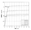
前記(3)式及び(4)式を使用して計算した結果の例を図7に示す。図7では、画素数が1280×1024=130万、電源電圧が3.3V、メモリCmの容量が40fF、抵抗はコラムごとにRcol=40kΩである場合を例にしており、チャネルポテンシャルの値は、1〜2Vの範囲での結果を示している。
図7から明らかなように、サンプリング時間を5μs以上にすれば、ほぼ安定したメモリCmの電圧である容量電圧Vs,j(t)が得られる。また、このときの増幅型固体撮像装置全体でのピーク電流は105mAになり、画素内に従来のような例えば1μAの定電流負荷を持つ場合の値1280mAと比較して、十分に小さい値になる。
FIG. 7 shows an example of a result calculated using the equations (3) and (4). FIG. 7 shows an example in which the number of pixels is 1280 × 1024 = 1.3 million, the power supply voltage is 3.3 V, the capacity of the memory Cm is 40 fF, and the resistance is Rcol = 40 kΩ for each column. The result in the range of 1-2V is shown.
As is apparent from FIG. 7, when the sampling time is set to 5 μs or more, the capacitance voltage Vs, j (t), which is a substantially stable voltage of the memory Cm, can be obtained. In addition, the peak current of the entire amplification type solid-state imaging device at this time is 105 mA, which is a sufficiently small value compared to a value of 1280 mA when the pixel has a constant current load of, for example, 1 μA as in the past. .
本発明の更なる利点として、低ノイズ化に有利ということがある。前記(1)式で示したような、従来型の画素構成では避けられなかったソースフォロワ負荷側で発生するノイズが、本発明では本質的に回避されている。更に、本発明は、次のような低ノイズ化の要因がある。通常は、画素内のメモリCmに信号を書き込む際、前記(2)式のようなノイズが発生し、このノイズはkTCノイズと言われ、避けることができない。 A further advantage of the present invention is that it is advantageous for reducing noise. The noise generated on the source follower load side, which is unavoidable in the conventional pixel configuration, as shown in the equation (1), is essentially avoided in the present invention. Furthermore, the present invention has the following noise reduction factors. Normally, when a signal is written to the memory Cm in the pixel, noise as expressed by the equation (2) is generated, which is called kTC noise and cannot be avoided.
しかし、本発明においては、図5に示したように、書き込みの最終段階ではサブスレッショルド領域動作であるモード2になり、この場合にはノイズは下記(5)式で表されることが知られている。これはソフトリセットモードと呼ばれ、ノイズ電力が通常動作の1/2になる。
However, in the present invention, as shown in FIG. 5, in the final stage of writing, the
図1において、第1の増幅トランジスタSF1における出力レベルの最大値は、図6においてV(UL)で示したように、電源電圧Vddに対してマージンを持つことが望ましい。ここで、V(UL)の値は、第1の増幅トランジスタSF1のしきい値及び接続部FDの電圧に依存し、接続部FDの電圧はリセットトランジスタRTのドレイン電圧Vrdに依存する。図1に例示するように、Vrd=Vddである場合には、第1の増幅トランジスタSF1のしきい値をエンハンスメント型にすることにより、前記マージンを確保し易くなる。又は、図示しないが、Vrd<Vddである場合には、第1の増幅トランジスタSF1のしきい値がデプレッション型であっても、前記マージンを確保することが容易になる。このようにして、図6におけるモード1の期間を短縮させることができ、書き込み動作全体の応答を早めることが可能になる。
In FIG. 1, the maximum value of the output level in the first amplification transistor SF1 desirably has a margin with respect to the power supply voltage Vdd, as indicated by V (UL) in FIG. Here, the value of V (UL) depends on the threshold value of the first amplification transistor SF1 and the voltage of the connection portion FD, and the voltage of the connection portion FD depends on the drain voltage Vrd of the reset transistor RT. As illustrated in FIG. 1, when Vrd = Vdd, it is easy to secure the margin by making the threshold value of the first amplification transistor SF1 an enhancement type. Alternatively, although not shown, when Vrd <Vdd, it is easy to ensure the margin even if the threshold value of the first amplification transistor SF1 is a depletion type. In this way, the period of
図1において、前記のような手法により第1の増幅トランジスタSF1における出力レベル、したがって第2の増幅トランジスタSF2の入力レベルの最大値を電源電圧Vddよりも低下させた場合、第2の増幅トランジスタSF2がエンハンスメント型であるとすると、図8に示すように、直線性の良い動作領域が低下する。なお、図8で示した入力とはゲート電圧を示しており、図8で示した出力とはソース電圧を示している。図8(a)は、第1及び第2の各増幅トランジスタSF1,SF2が共にエンハンスメント型である場合の、第1及び第2の各増幅トランジスタSF1,SF2における入出力電圧の関係例を示している。 In FIG. 1, when the output level of the first amplifying transistor SF1, and hence the maximum value of the input level of the second amplifying transistor SF2, is lowered below the power supply voltage Vdd by the above-described method, the second amplifying transistor SF2 If is an enhancement type, as shown in FIG. 8, the operating region with good linearity is lowered. The input shown in FIG. 8 indicates the gate voltage, and the output shown in FIG. 8 indicates the source voltage. FIG. 8A shows an example of the relationship between the input and output voltages of the first and second amplification transistors SF1 and SF2 when the first and second amplification transistors SF1 and SF2 are both of the enhancement type. Yes.
SF1iで示した第1の増幅トランジスタSF1の入力電圧、すなわちゲート電圧に対して、該出力電圧、すなわちソース電圧はSF1oになり、この電圧が第2の増幅トランジスタSF2のゲート電圧である入力電圧SF2iになる。図8(a)から明らかなように、第2の増幅トランジスタSF2の動作領域の下限付近は直線性から外れた領域になっている。これに対して、図8(b)に示すように、第2の増幅トランジスタSF2をデプレッション型にすることにより、第2の増幅トランジスタSF2の入力電圧SF2iが小さくなっても、第2の増幅トランジスタSF2の動作マージンを十分に確保することができる。 The output voltage, that is, the source voltage is SF1o with respect to the input voltage, that is, the gate voltage of the first amplifying transistor SF1 indicated by SF1i, and this voltage is the gate voltage of the second amplifying transistor SF2. become. As is clear from FIG. 8A, the vicinity of the lower limit of the operation region of the second amplification transistor SF2 is a region deviating from linearity. On the other hand, as shown in FIG. 8B, even if the input voltage SF2i of the second amplifying transistor SF2 is reduced by making the second amplifying transistor SF2 a depletion type, the second amplifying transistor A sufficient operating margin of SF2 can be secured.
また、図1において、メモリCmの少なくとも一部をMOS型容量にすることにより、容量密度(単位面積当たりの容量)を高めることが可能となり、限られた画素面積内で十分なメモリCmの容量値を確保し易くなる。更に、前記MOS型容量をデプレッション型にすればメモリCmの容量値を確保することができる動作電圧範囲を低い側へ拡大させることができ、前記のように、第1の増幅トランジスタSF1の出力電圧SF1oが低下しても、一定のメモリCmの容量値を確保しやすくすることができる。 Further, in FIG. 1, by making at least a part of the memory Cm a MOS type capacitor, it is possible to increase the capacity density (capacity per unit area), and the capacity of the memory Cm sufficient within a limited pixel area. It becomes easy to secure the value. Further, if the MOS type capacitor is made a depletion type, the operating voltage range in which the capacity value of the memory Cm can be secured can be expanded to the lower side, and as described above, the output voltage of the first amplification transistor SF1. Even if SF1o decreases, it is possible to easily secure a certain capacity value of the memory Cm.
なお、図1において、転送トランジスタTXを省略して3トランジスタ型の画素を構成するようにしてもよく、このようにした場合、図1は図9のようになる。図9のようにした場合においても、メモリCmへの書き込み、及びメモリCmからの読み出しは、図1の場合と同様である。 In FIG. 1, the transfer transistor TX may be omitted to form a three-transistor pixel. In such a case, FIG. 1 becomes as shown in FIG. Even in the case of FIG. 9, the writing to the memory Cm and the reading from the memory Cm are the same as in the case of FIG.
第2の実施の形態.
図10は、本発明の第2の実施の形態における増幅型固体撮像装置の画素構成の例を示した図である。なお、図10では、図1と同じもの又は同様のものは同じ符号で示し、ここではその説明を省略すると共に図1との相違点のみ説明する。
図10における図1との相違点は、画素内のメモリをCm1とCm2の2個にし、これに伴って2つの書き込みスイッチWr1,Wr2と、2つの読み出しスイッチRd1,Rd2を備えたことにあり、これらのことから図1の画素10を画素50にした。
Second embodiment.
FIG. 10 is a diagram illustrating an example of a pixel configuration of an amplification type solid-state imaging device according to the second embodiment of the present invention. In FIG. 10, the same or similar elements as those in FIG. 1 are denoted by the same reference numerals, and the description thereof will be omitted here, and only the differences from FIG. 1 will be described.
The difference between FIG. 10 and FIG. 1 is that the number of memories in the pixel is two, Cm1 and Cm2, and two write switches Wr1 and Wr2 and two read switches Rd1 and Rd2 are provided accordingly. Therefore, the
図10において、画素50は、受光素子PD、転送トランジスタTX、リセットトランジスタRT、第1の増幅トランジスタSF1、選択トランジスタSL、第2の増幅トランジスタSF2、第1及び第2の各書き込みスイッチWr1,Wr2、第1及び第2の各読み出しスイッチRd1,Rd2、第1及び第2の各メモリCm1,Cm2及び第1及び第2の各メモリCm1,Cm2を初期化する初期化トランジスタITを備えている。第1及び第2の各書き込みスイッチWr1,Wr2、並びに第1及び第2の各読み出しスイッチRd1,Rd2は、それぞれNMOSトランジスタからなる。なお、メモリCm1は第1の容量を、メモリCm2は第2の容量をそれぞれなし、第1の書き込みスイッチWr1は第1の書き込みスイッチ部を、第2の書き込みスイッチWr2は第2の書き込みスイッチ部を、第1の読み出しスイッチRd1は第1の読み出しスイッチ部を、第2の読み出しスイッチRd2は第2の読み出しスイッチ部をそれぞれなす。
In FIG. 10, a
第2の増幅トランジスタSF2のゲートと初期化トランジスタITとの接続部をFD2とすると、第1の増幅トランジスタSF1のソースと接続部FD2との間に、第1の書き込みトランジスタWr1及び第1の読み出しトランジスタRd1の直列回路と、第2の書き込みトランジスタWr2及び第2の読み出しトランジスタRd2の直列回路が並列に接続されている。第1の書き込みトランジスタWr1と第1の読み出しトランジスタRd1との接続部と接地電圧との間に第1のメモリCm1が接続され、第2の書き込みトランジスタWr2と第2の読み出しトランジスタRd2との接続部と接地電圧との間に第2のメモリCm2が接続されている。 When the connection portion between the gate of the second amplification transistor SF2 and the initialization transistor IT is FD2, the first write transistor Wr1 and the first read transistor are connected between the source of the first amplification transistor SF1 and the connection portion FD2. A series circuit of the transistor Rd1 and a series circuit of the second write transistor Wr2 and the second read transistor Rd2 are connected in parallel. The first memory Cm1 is connected between the connection between the first write transistor Wr1 and the first read transistor Rd1 and the ground voltage, and the connection between the second write transistor Wr2 and the second read transistor Rd2. And the ground voltage are connected to the second memory Cm2.
なお、図10の画素50をマトリクス状に配置した画素アレイを含む2次元イメージセンサの構成例を示した図は、図2及び図3の画素10の符号を50に変える以外は同じであることから省略する。第1及び第2の各書き込みスイッチWr1,Wr2、並びに第1及び第2の各読み出しスイッチRd1,Rd2は、それぞれ信号線16を介して行駆動回路15からの制御信号がゲートに入力される。
このような構成において、図11は、図10で示した画素50の動作例を示したタイミングチャートであり、図11を用いて図10の画素50の動作について説明する。
10 is a diagram illustrating a configuration example of a two-dimensional image sensor including a pixel array in which the
In such a configuration, FIG. 11 is a timing chart showing an operation example of the
書き込み動作は全行とも同時動作になる。図11において、まず期間t1でリセットトランジスタRTをオン/オフさせて接続部FDの電圧をリセットし、次に、期間t2において、第1の書き込みスイッチWr1をオンさせ、このときの接続部FDの電圧を前記図4から図7で説明した本発明の書き込み動作により、リセットレベルFRとして第1のメモリCm1に書き込む。
次に、期間t3で、転送トランジスタTXをオンさせて信号電荷を接続部FDに転送し、期間t4で、第2の書き込みスイッチWr2をオンさせて該信号電荷によって変化した接続部FDの電圧を信号レベルFSとして、前記t2の場合と同様の書き込み動作により第2のメモリCm2に書き込む。最後に、期間t5で、リセットトランジスタRTを再度オン/オフさせて接続部FDの信号電荷を排出して接続部FDをリセットする。このようにして、各画素単位で、2つのメモリCm1及びCm2に、リセットレベルFR及び信号レベルFSを独立に全行一括して書き込むことができる。
The write operation is simultaneous for all rows. In FIG. 11, first, the reset transistor RT is turned on / off in the period t1 to reset the voltage of the connection portion FD, and then in the period t2, the first write switch Wr1 is turned on, and the connection portion FD at this time The voltage is written to the first memory Cm1 as the reset level FR by the write operation of the present invention described with reference to FIGS.
Next, in period t3, the transfer transistor TX is turned on to transfer the signal charge to the connection part FD, and in period t4, the second write switch Wr2 is turned on to change the voltage of the connection part FD changed by the signal charge. The signal level FS is written into the second memory Cm2 by the same write operation as in the case of t2. Finally, in the period t5, the reset transistor RT is turned on / off again to discharge the signal charge of the connection portion FD and reset the connection portion FD. In this manner, the reset level FR and the signal level FS can be independently written in a batch for each pixel in the two memories Cm1 and Cm2.
各メモリCm1及びCm2に書き込まれた信号の読み出しは行単位で順次行われる。例えば任意のi行目について示すと次のようになる。なお、符号において、(i)はi行目のものであることを示し、(i+1)は(i+1)行目のものであることを示している。
まず、期間t6で、初期化トランジスタIT(i)をオン/オフさせて、2段目のソースフォロワをなす第2の増幅トランジスタSF2(i)のゲート電圧になる接続部FD2(i)の電圧を接地電圧等の低電圧V1に初期化する。
次に、期間t7で、第2の増幅トランジスタSF2(i)と読み出し信号線Vsigとの間の選択トランジスタSL(i)をオンさせた後、読み出しスイッチRd1(i)をオンさせて、第1のメモリCm1(i)に保持されたリセットレベルFRを読み出す。
Reading of signals written in the memories Cm1 and Cm2 is sequentially performed in units of rows. For example, an arbitrary i-th row is as follows. In the reference numerals, (i) indicates the i-th row and (i + 1) indicates the (i + 1) -th row.
First, in the period t6, the initialization transistor IT (i) is turned on / off, and the voltage of the connection FD2 (i) that becomes the gate voltage of the second amplification transistor SF2 (i) that forms the second-stage source follower. Is initialized to a low voltage V1 such as a ground voltage.
Next, in a period t7, after the selection transistor SL (i) between the second amplification transistor SF2 (i) and the read signal line Vsig is turned on, the read switch Rd1 (i) is turned on, and the first The reset level FR held in the memory Cm1 (i) is read out.
次に、期間t8で、初期化トランジスタIT(i)を再度オン/オフさせて、先に読み出した信号を消去して接続部FD2の電圧をリセットする。
期間t9では、第2の読み出しスイッチRd2(i)をオンさせて、第2のメモリCm2(i)に保持された信号レベルFSを読み出す。
期間t10では、選択トランジスタSL(i)をオフさせ、初期化トランジスタIT(i)をオンさせると共に第1及び第2の各読み出しスイッチRd1(i),Rd2(i)をそれぞれオンさせ、2つの第1及び第2の各メモリCm1,Cm2を同時に低電圧V1にリセットし、次のフレームでの書き込み動作に備える。
Next, in a period t8, the initialization transistor IT (i) is turned on / off again to erase the signal read out earlier and reset the voltage of the connection portion FD2.
In a period t9, the second read switch Rd2 (i) is turned on to read the signal level FS held in the second memory Cm2 (i).
In the period t10, the selection transistor SL (i) is turned off, the initialization transistor IT (i) is turned on, and each of the first and second read switches Rd1 (i) and Rd2 (i) is turned on. The first and second memories Cm1 and Cm2 are simultaneously reset to the low voltage V1 to prepare for a write operation in the next frame.
このようにして、読み出された2つの信号FR及びFSについて、図示しないが後段の処理回路で両者の差分を取る相関二重サンプリング(CDS)動作を行うことにより、接続部FDで発生するリセットノイズを除去することができるだけでなく、1段目ソースフォロワをなす第1の増幅トランジスタSF1及び2段目ソースフォロワをなす第2の増幅トランジスタSF2のそれぞれにおいて、しきい値が画素間でばらつくことによって発生する、画素ごとの固定パターンノイズをも除去することができる。 In this way, with respect to the two signals FR and FS read out, a reset that occurs in the connection unit FD is performed by performing a correlated double sampling (CDS) operation that takes a difference between the two in a subsequent processing circuit (not shown). Not only can noise be removed, but the threshold value varies between pixels in each of the first amplification transistor SF1 forming the first-stage source follower and the second amplification transistor SF2 forming the second-stage source follower. It is possible to remove the fixed pattern noise generated for each pixel.
なお、図10において、選択トランジスタSLを省略するようにしてもよく、このようにした場合、図10は図12のようになる。なお、図12の画素50をマトリクス状に配置した画素アレイを含む2次元イメージセンサの構成例を示した図においても、図2及び図3の画素10の符号を50に変える以外は同じであることから省略する。
このような構成において、図13は、図12の画素50における動作例を示したタイミングチャートであり、図13を用いて図12の画素50の動作について説明する。
In FIG. 10, the selection transistor SL may be omitted. In such a case, FIG. 10 becomes as shown in FIG. 12 is the same as the configuration example of the two-dimensional image sensor including the pixel array in which the
In such a configuration, FIG. 13 is a timing chart showing an operation example of the
図13において、書き込み動作は図11と同じであるのでその説明を省略する。なお、図13においても、各メモリCm1及びCm2に書き込まれた信号の読み出しは行単位で順次行われ、例えば任意のi行目について示すと次のようになる。図13の符号においても、(i)はi行目のものであることを示し、(i+1)は(i+1)行目のものであることを示している。
図12では、初期化トランジスタITをノーマリオン(読み出し動作時以外はオン)にする。したがって、読み出し動作では、非選択行ではすべての初期化トランジスタITがオンしており、これらの画素では、接続部FD2が接地電圧等の低電圧V1に固定される。このため、ソースフォロワをなしている第2の増幅トランジスタSF2はオフする。
In FIG. 13, the write operation is the same as in FIG. Also in FIG. 13, reading of signals written in the memories Cm1 and Cm2 is sequentially performed in units of rows. For example, an arbitrary i-th row is as follows. Also in the code | symbol of FIG. 13, (i) shows that it is the thing of the i-th line, (i + 1) has shown that it is the thing of the (i + 1) -th line.
In FIG. 12, the initialization transistor IT is normally turned on (on except during the read operation). Therefore, in the read operation, all the initialization transistors IT are turned on in the non-selected rows, and in these pixels, the connection portion FD2 is fixed to the low voltage V1 such as the ground voltage. For this reason, the second amplifying transistor SF2 constituting the source follower is turned off.
読み出し行iにおいては、期間t7と期間t9においてのみ、初期化トランジスタIT(i)がオフし、接続部FD2(i)はフローティング状態になる。期間t7では、この間に第1の読み出しトランジスタRd1(i)がオンし、第1のメモリCm1(i)からリセットレベルFRが接続部FD2(i)に読み出され、接続部FD2(i)の電圧がこれに対応した大きい電圧になる。このため、このような行iのみ第2の増幅トランジスタSF2(i)はオンし、行iのリセットレベルFRが選択的に読み出される。 In the read row i, the initialization transistor IT (i) is turned off only in the periods t7 and t9, and the connection portion FD2 (i) is in a floating state. In the period t7, the first read transistor Rd1 (i) is turned on during this period, the reset level FR is read from the first memory Cm1 (i) to the connection portion FD2 (i), and the connection portion FD2 (i) The voltage becomes a large voltage corresponding to this. Therefore, the second amplification transistor SF2 (i) is turned on only in such row i, and the reset level FR of row i is selectively read out.
同様に、期間t9では、この間に第2の読み出しスイッチRd2(i)がオンし、第2のメモリCm2(i)から信号レベルFSが接続部FD2(i)に読み出され、接続部FD2(i)の電圧がこれに対応した大きい電圧になって、この行iの信号レベルFSが選択的に読み出される。動作範囲としては、FR≧FSであることから、FS>V1であれば非選択行の影響を受けずに読み出しを行うことができる。また、図示しない後段の処理回路で、リセットレベルFRと信号レベルFSの差分を取るCDS動作を行うことも、図10及び図11の場合と同様である。 Similarly, in the period t9, the second read switch Rd2 (i) is turned on during this period, the signal level FS is read from the second memory Cm2 (i) to the connection unit FD2 (i), and the connection unit FD2 ( The voltage i) becomes a large voltage corresponding thereto, and the signal level FS of this row i is selectively read out. Since the operation range is FR ≧ FS, if FS> V1, reading can be performed without being affected by the non-selected rows. Further, the CDS operation for taking the difference between the reset level FR and the signal level FS in the subsequent processing circuit (not shown) is the same as in the case of FIGS.
第3の実施の形態.
前記第2の実施の形態で示した画素構成の場合、期間t1でリセットトランジスタRTをオンさせて接続部FDをリセットする際、第1の増幅トランジスタSF1の出力側Vaがフローティング状態になって電圧が不定になるため、接続部FDと出力側Vaとの間の容量Caに不定電圧情報がメモリされる。これは、次にリセットトランジスタRTをオフさせて接続部FDをフローティング状態にすると、容量Caを介して接続部FDの電圧が前記不定電圧情報に影響され、誤差が生じる。このような誤差をなくすようにしたものを本発明の第3の実施の形態とする。
Third embodiment.
In the case of the pixel configuration shown in the second embodiment, when the reset transistor RT is turned on in the period t1 to reset the connection portion FD, the output side Va of the first amplifying transistor SF1 is in a floating state, and the voltage Therefore, the indefinite voltage information is stored in the capacitor Ca between the connecting portion FD and the output side Va. This is because when the reset transistor RT is turned off and the connecting portion FD is in a floating state, the voltage of the connecting portion FD is influenced by the indefinite voltage information through the capacitor Ca, and an error occurs. A configuration in which such an error is eliminated is referred to as a third embodiment of the present invention.
図14は、本発明の第3の実施形態における増幅型固体撮像装置の画素構成の例を示した図である。なお、図14では、図10と同じもの又は同様のものは同じ符号で示し、ここではその説明を省略すると共に図10との相違点のみ説明する。
図14における図10との相違点は、第1の増幅トランジスタSF1に並列にNMOSトランジスタである制御スイッチWr3を接続したことにあり、これに伴って、図10の画素50を画素60にした。なお、制御スイッチWr3は制御スイッチ部をなす。
図14において、制御スイッチWr3がオンしているときには、第1の増幅トランジスタSF1の出力側Vaの電圧が電源電圧Vddになるように、制御スイッチWr3をデプレッション型のMOSトランジスタにすることが望ましい。あるいは、図示しないが、制御スイッチWr3のドレイン側を電源電圧Vddとは異なる所定のDC電圧としてもよい。
FIG. 14 is a diagram illustrating an example of a pixel configuration of an amplification type solid-state imaging device according to the third embodiment of the present invention. In FIG. 14, the same or similar parts as those in FIG. 10 are denoted by the same reference numerals, and description thereof is omitted here, and only differences from FIG. 10 are described.
14 differs from FIG. 10 in that a control switch Wr3, which is an NMOS transistor, is connected in parallel to the first amplification transistor SF1, and accordingly, the
In FIG. 14, when the control switch Wr3 is on, it is desirable that the control switch Wr3 be a depletion type MOS transistor so that the voltage on the output side Va of the first amplification transistor SF1 becomes the power supply voltage Vdd. Alternatively, although not shown, the drain side of the control switch Wr3 may be a predetermined DC voltage different from the power supply voltage Vdd.
図14において、画素60は、受光素子PD、転送トランジスタTX、リセットトランジスタRT、第1の増幅トランジスタSF1、選択トランジスタSL、第2の増幅トランジスタSF2、第1及び第2の各書き込みスイッチWr1,Wr2、第1及び第2の各読み出しスイッチRd1,Rd2、制御スイッチWr3、第1及び第2の各メモリCm1,Cm2及び第1及び第2の各メモリCm1,Cm2を初期化するための初期化トランジスタITを備えている。
なお、図14の画素60をマトリクス状に配置した画素アレイを含む2次元イメージセンサの構成例を示した図は、図2及び図3の画素10の符号を60に変える以外は同じであることから省略する。制御スイッチWr3は、信号線16を介して行駆動回路15からの制御信号がゲートに入力される。
In FIG. 14, a
14 is a diagram showing a configuration example of a two-dimensional image sensor including a pixel array in which the
このような構成において、図15は、図14で示した画素60の動作例を示したタイミングチャートであり、図15を用いて図14の画素60の動作について説明する。
図15において、まず最初のリセット期間t1内の期間taにおいて、リセットトランジスタRTと制御スイッチWr3を同時にオンさせて、接続部FDをリセットすると共に出力側Vaの電圧を電源電圧Vddにすることにより、容量Caには確定した電圧情報が書き込まれる。この後、期間t2〜t5では、図11で示した動作が誤差を生じることなく行われる。このような動作は、全画素一括して行われ、その後の読み出し動作は、図11の場合とまったく同じである。
In such a configuration, FIG. 15 is a timing chart showing an operation example of the
In FIG. 15, first, in the period ta within the first reset period t1, the reset transistor RT and the control switch Wr3 are simultaneously turned on to reset the connection portion FD and set the voltage on the output side Va to the power supply voltage Vdd. The determined voltage information is written in the capacitor Ca. Thereafter, in the period t2 to t5, the operation shown in FIG. 11 is performed without causing an error. Such an operation is performed collectively for all the pixels, and the subsequent readout operation is exactly the same as in FIG.
なお、前記第1から第3の各実施形態では、画素内の各MOSトランジスタがNMOS型である場合を例にして説明したが、これは一例であり、本発明はこれに限定するものではなく、PMOS型の場合についても、電圧、電流の極性を逆にすることによって同様に適用することができる。また、受光素子PDの信号電荷が電子である場合を例にして説明したが、正孔である場合においても信号蓄積による極性変化が逆になることで、同様に適用することができる。 In each of the first to third embodiments, the case where each MOS transistor in the pixel is an NMOS type has been described as an example. However, this is an example, and the present invention is not limited to this. The case of the PMOS type can be similarly applied by reversing the polarity of the voltage and current. Further, the case where the signal charge of the light receiving element PD is an electron has been described as an example. However, even in the case of a hole, the present invention can be similarly applied because the polarity change due to signal accumulation is reversed.
10,50,60 画素
PD 受光素子
TX 転送トランジスタ
RT リセットトランジスタ
SF1 第1の増幅トランジスタ
SF2 第2の増幅トランジスタ
Wr 書き込みスイッチ
SL 選択トランジスタ
IT 初期化トランジスタ
Cm メモリ
Wr1 第1の書き込みスイッチ
Wr2 第2の書き込みスイッチ
Wr3 制御スイッチ
Rd1 第1の読み出しスイッチ
Rd2 第2の読み出しスイッチ
Cm1 第1のメモリ
Cm2 第2のメモリ
R,Rcol,Rfrm 抵抗
CL 定電流負荷トランジスタ
11,12,13 電源線
14 行デコーダ回路
15 行駆動回路
16 駆動線
17 コラム信号処理回路
18 コラムデコーダ回路
19 水平信号線
20 画素アレイ
10, 50, 60 pixels PD light receiving element TX transfer transistor RT reset transistor SF1 first amplification transistor SF2 second amplification transistor Wr write switch SL selection transistor IT initialization transistor Cm memory Wr1 first write switch Wr2 second write Switch Wr3 Control switch Rd1 First read switch Rd2 Second read switch Cm1 First memory Cm2 Second memory R, Rcol, Rfrm Resistance CL Constant
Claims (12)
前記各画素は、
受光した光に応じた信号を生成して出力する光電変換部と、
該光電変換部から出力された信号がゲートに入力され、該ゲートに入力された信号を増幅して出力するMOSトランジスタからなる第1の増幅トランジスタと、
該第1の増幅トランジスタから出力された信号を記憶するための前記メモリをなす第1の容量と、
前記第1の増幅トランジスタから出力された信号に対して、該第1の容量への出力制御を行って該第1の容量への書き込み制御を行う第1の書き込みスイッチ部と、
前記第1の容量に書き込まれた信号がゲートに入力され、該ゲートに入力された信号を増幅して出力するMOSトランジスタからなる第2の増幅トランジスタと、
前記第1の容量に書き込まれた信号を所定の第1電圧に初期化する初期化トランジスタと、
をそれぞれ備え、
前記第1の増幅トランジスタは、前記第1の容量のみを負荷とし、前記第1の書き込みスイッチ部は、前記初期化トランジスタによって前記第1の容量に対する前記初期化が行われた後、前記第1の増幅トランジスタが飽和領域動作からサブスレッショルド領域動作に移行して準安定状態になる期間、前記第1の増幅トランジスタから出力された信号を前記第1の容量へ出力して前記第1の容量への書き込みを行うことを特徴とする増幅型固体撮像装置。 In an amplification type solid-state imaging device including a pixel array in which a plurality of unit pixels each having a memory are arranged in a matrix, and a control circuit unit that performs operation control on each pixel constituting the pixel array,
Each pixel is
A photoelectric conversion unit that generates and outputs a signal corresponding to the received light; and
A first amplification transistor composed of a MOS transistor for inputting a signal output from the photoelectric conversion unit to a gate and amplifying and outputting the signal input to the gate;
A first capacitor forming the memory for storing a signal output from the first amplification transistor;
A first write switch unit that performs output control to the first capacitor to control writing to the first capacitor with respect to a signal output from the first amplification transistor;
A second amplifying transistor comprising a MOS transistor for inputting a signal written in the first capacitor to a gate and amplifying and outputting the signal input to the gate;
An initialization transistor for initializing a signal written in the first capacitor to a predetermined first voltage;
Each with
The first amplifying transistor uses only the first capacitor as a load, and the first write switch unit performs the initialization after the initialization of the first capacitor is performed by the initialization transistor. During the period in which the amplifying transistor shifts from the saturation region operation to the subthreshold region operation and becomes a metastable state, the signal output from the first amplifying transistor is output to the first capacitor to the first capacitor. An amplifying solid-state imaging device, wherein
前記第1の増幅トランジスタから出力された信号を記憶するための前記メモリをなす1つ以上の第2の容量と、
前記第1の増幅トランジスタから出力された信号に対して、対応する該第2の容量への出力制御を行って該第2の容量への書き込み制御を行う1つ以上の第2の書き込みスイッチ部と、
前記第1の容量に書き込まれた信号に対して、前記第2の増幅トランジスタのゲートへの出力制御を行う第1の読み出しスイッチ部と、
対応する前記第2の容量に書き込まれた信号に対して、前記第2の増幅トランジスタのゲートへの出力制御を行う1つ以上の第2の読み出しスイッチ部と、
を備え、
前記第1の増幅トランジスタは、前記第1又は第2の容量のみを負荷とし、前記初期化トランジスタは、前記第2の容量に書き込まれた信号を前記所定の第1電圧に初期化し、前記第2の書き込みスイッチ部は、前記初期化トランジスタによって前記第2の容量に対する前記初期化が行われた後、前記第1の増幅トランジスタが飽和領域動作からサブスレッショルド領域動作に移行して準安定状態になる期間、前記第1の増幅トランジスタから出力された信号を前記第2の容量へ出力して前記第2の容量への書き込みを行うことを特徴とする請求項1〜5のうちのいずれか1つに記載の増幅型固体撮像装置。 Each pixel is
One or more second capacitors forming the memory for storing a signal output from the first amplification transistor;
One or more second write switch units for performing output control to the corresponding second capacitor and controlling writing to the second capacitor with respect to the signal output from the first amplification transistor When,
A first read switch unit for controlling output to the gate of the second amplification transistor with respect to a signal written to the first capacitor;
One or more second read switch units for controlling output to the gate of the second amplification transistor with respect to a signal written in the corresponding second capacitor;
With
The first amplification transistor uses only the first or second capacitor as a load, and the initialization transistor initializes a signal written in the second capacitor to the predetermined first voltage, and In the second write switch unit, after the initialization of the second capacitor is performed by the initialization transistor, the first amplification transistor shifts from a saturation region operation to a subthreshold region operation to be in a metastable state. The signal output from the first amplifying transistor is output to the second capacitor during a period, and writing to the second capacitor is performed. Amplifying solid-state imaging device described in 1.
Priority Applications (1)
| Application Number | Priority Date | Filing Date | Title |
|---|---|---|---|
| JP2009019218A JP4957925B2 (en) | 2009-01-30 | 2009-01-30 | Amplification type solid-state imaging device |
Applications Claiming Priority (1)
| Application Number | Priority Date | Filing Date | Title |
|---|---|---|---|
| JP2009019218A JP4957925B2 (en) | 2009-01-30 | 2009-01-30 | Amplification type solid-state imaging device |
Publications (3)
| Publication Number | Publication Date |
|---|---|
| JP2010178117A JP2010178117A (en) | 2010-08-12 |
| JP2010178117A5 JP2010178117A5 (en) | 2012-02-16 |
| JP4957925B2 true JP4957925B2 (en) | 2012-06-20 |
Family
ID=42708615
Family Applications (1)
| Application Number | Title | Priority Date | Filing Date |
|---|---|---|---|
| JP2009019218A Expired - Fee Related JP4957925B2 (en) | 2009-01-30 | 2009-01-30 | Amplification type solid-state imaging device |
Country Status (1)
| Country | Link |
|---|---|
| JP (1) | JP4957925B2 (en) |
Cited By (1)
| Publication number | Priority date | Publication date | Assignee | Title |
|---|---|---|---|---|
| US10446595B2 (en) | 2015-06-08 | 2019-10-15 | Ricoh Company, Ltd. | Solid-state imaging device |
Families Citing this family (9)
| Publication number | Priority date | Publication date | Assignee | Title |
|---|---|---|---|---|
| JP5369779B2 (en) * | 2009-03-12 | 2013-12-18 | ソニー株式会社 | Solid-state imaging device, driving method of solid-state imaging device, and electronic apparatus |
| US8987646B2 (en) * | 2011-06-10 | 2015-03-24 | Semiconductor Components Industries, Llc | Pixel and method |
| JP5995457B2 (en) * | 2012-02-17 | 2016-09-21 | キヤノン株式会社 | Imaging device, imaging system, and driving method of imaging device. |
| JP5814818B2 (en) * | 2012-02-21 | 2015-11-17 | 株式会社日立製作所 | Solid-state imaging device |
| JP6265655B2 (en) * | 2012-10-09 | 2018-01-24 | キヤノン株式会社 | Detection device and detection system |
| JP6612492B2 (en) | 2014-10-16 | 2019-11-27 | 株式会社リコー | Photoelectric conversion element, image reading apparatus, and image forming apparatus |
| JP6740230B2 (en) * | 2015-07-31 | 2020-08-12 | ソニーセミコンダクタソリューションズ株式会社 | Solid-state imaging device and electronic device |
| JP7330124B2 (en) * | 2020-03-19 | 2023-08-21 | 株式会社東芝 | Solid-state imaging device |
| JP2022181579A (en) * | 2021-05-26 | 2022-12-08 | ソニーセミコンダクタソリューションズ株式会社 | Solid-state image capture element and electronic apparatus |
Family Cites Families (7)
| Publication number | Priority date | Publication date | Assignee | Title |
|---|---|---|---|---|
| JP4345175B2 (en) * | 2000-02-01 | 2009-10-14 | コニカミノルタホールディングス株式会社 | Solid-state imaging device |
| JP4724313B2 (en) * | 2001-05-18 | 2011-07-13 | キヤノン株式会社 | Imaging apparatus, radiation imaging apparatus, and radiation imaging system using the same |
| JP4288346B2 (en) * | 2003-08-19 | 2009-07-01 | 国立大学法人静岡大学 | Imaging device and pixel circuit |
| JP2006311515A (en) * | 2005-03-29 | 2006-11-09 | Konica Minolta Holdings Inc | Solid-state image-sensing device |
| JP2007329722A (en) * | 2006-06-08 | 2007-12-20 | Matsushita Electric Ind Co Ltd | Solid-state imaging element and digital camera |
| JP2008017288A (en) * | 2006-07-07 | 2008-01-24 | Rohm Co Ltd | Photoelectric conversion circuit, and solid-state imaging apparatus using this |
| JP5012188B2 (en) * | 2007-05-14 | 2012-08-29 | コニカミノルタホールディングス株式会社 | Solid-state imaging device |
-
2009
- 2009-01-30 JP JP2009019218A patent/JP4957925B2/en not_active Expired - Fee Related
Cited By (2)
| Publication number | Priority date | Publication date | Assignee | Title |
|---|---|---|---|---|
| US10446595B2 (en) | 2015-06-08 | 2019-10-15 | Ricoh Company, Ltd. | Solid-state imaging device |
| US10868057B2 (en) | 2015-06-08 | 2020-12-15 | Ricoh Company, Ltd. | Solid-state imaging device |
Also Published As
| Publication number | Publication date |
|---|---|
| JP2010178117A (en) | 2010-08-12 |
Similar Documents
| Publication | Publication Date | Title |
|---|---|---|
| JP4957925B2 (en) | Amplification type solid-state imaging device | |
| KR101450904B1 (en) | A/d conversion circuit, control method thereof, solid-state imaging device, and imaging apparatus | |
| JP4846076B1 (en) | Amplification type solid-state imaging device | |
| JP5098831B2 (en) | Solid-state imaging device and camera system | |
| JP6482186B2 (en) | Imaging apparatus and driving method thereof | |
| JP6319946B2 (en) | Solid-state imaging device and imaging system | |
| WO2017179319A1 (en) | Solid-state imaging element, electronic device and control method for solid-state imaging element | |
| JP5066996B2 (en) | Solid-state imaging device, signal processing method for solid-state imaging device, and imaging device | |
| JP6385193B2 (en) | Solid-state imaging device and imaging system | |
| JP4695967B2 (en) | Solid-state imaging device and camera | |
| JP6561315B2 (en) | Solid-state imaging device | |
| JP2016005054A (en) | Solid-state image pickup device | |
| CN113259606B (en) | Image sensor for implementing high dynamic range image using dual conversion gain | |
| JP2005295346A (en) | Amplification type solid-state imaging apparatus | |
| WO2011083541A1 (en) | Solid-state image capture device and image capture device | |
| JP4666383B2 (en) | Amplification type solid-state imaging device and electronic information device | |
| JP4661212B2 (en) | Physical information acquisition method, physical information acquisition device, and semiconductor device | |
| JP4048415B2 (en) | Solid-state imaging device and driving method thereof | |
| JP5177198B2 (en) | Physical information acquisition method and physical information acquisition device | |
| JP5893329B2 (en) | Imaging apparatus and endoscope apparatus | |
| US20180007298A1 (en) | Imaging device | |
| JP2017055370A (en) | Solid-state imaging apparatus | |
| JP5197440B2 (en) | Photoelectric conversion device | |
| JP6060500B2 (en) | Image sensor | |
| JP2011087125A (en) | Solid-state imaging element |
Legal Events
| Date | Code | Title | Description |
|---|---|---|---|
| A521 | Request for written amendment filed |
Free format text: JAPANESE INTERMEDIATE CODE: A523 Effective date: 20111227 |
|
| A621 | Written request for application examination |
Free format text: JAPANESE INTERMEDIATE CODE: A621 Effective date: 20111227 |
|
| A871 | Explanation of circumstances concerning accelerated examination |
Free format text: JAPANESE INTERMEDIATE CODE: A871 Effective date: 20111227 |
|
| A975 | Report on accelerated examination |
Free format text: JAPANESE INTERMEDIATE CODE: A971005 Effective date: 20120127 |
|
| A131 | Notification of reasons for refusal |
Free format text: JAPANESE INTERMEDIATE CODE: A131 Effective date: 20120131 |
|
| A521 | Request for written amendment filed |
Free format text: JAPANESE INTERMEDIATE CODE: A523 Effective date: 20120203 |
|
| TRDD | Decision of grant or rejection written | ||
| A01 | Written decision to grant a patent or to grant a registration (utility model) |
Free format text: JAPANESE INTERMEDIATE CODE: A01 Effective date: 20120221 |
|
| A01 | Written decision to grant a patent or to grant a registration (utility model) |
Free format text: JAPANESE INTERMEDIATE CODE: A01 |
|
| A61 | First payment of annual fees (during grant procedure) |
Free format text: JAPANESE INTERMEDIATE CODE: A61 Effective date: 20120306 |
|
| FPAY | Renewal fee payment (event date is renewal date of database) |
Free format text: PAYMENT UNTIL: 20150330 Year of fee payment: 3 |
|
| R150 | Certificate of patent or registration of utility model |
Ref document number: 4957925 Country of ref document: JP Free format text: JAPANESE INTERMEDIATE CODE: R150 Free format text: JAPANESE INTERMEDIATE CODE: R150 |
|
| R250 | Receipt of annual fees |
Free format text: JAPANESE INTERMEDIATE CODE: R250 |
|
| R250 | Receipt of annual fees |
Free format text: JAPANESE INTERMEDIATE CODE: R250 |
|
| LAPS | Cancellation because of no payment of annual fees |