JP4953820B2 - Method for manufacturing fin-type FET - Google Patents
Method for manufacturing fin-type FET Download PDFInfo
- Publication number
- JP4953820B2 JP4953820B2 JP2006538523A JP2006538523A JP4953820B2 JP 4953820 B2 JP4953820 B2 JP 4953820B2 JP 2006538523 A JP2006538523 A JP 2006538523A JP 2006538523 A JP2006538523 A JP 2006538523A JP 4953820 B2 JP4953820 B2 JP 4953820B2
- Authority
- JP
- Japan
- Prior art keywords
- fin
- layer
- forming
- silicon
- type fet
- Prior art date
- Legal status (The legal status is an assumption and is not a legal conclusion. Google has not performed a legal analysis and makes no representation as to the accuracy of the status listed.)
- Expired - Fee Related
Links
- 238000000034 method Methods 0.000 title claims description 28
- 238000004519 manufacturing process Methods 0.000 title description 30
- 239000010410 layer Substances 0.000 claims description 58
- 239000011241 protective layer Substances 0.000 claims description 29
- XUIMIQQOPSSXEZ-UHFFFAOYSA-N Silicon Chemical compound [Si] XUIMIQQOPSSXEZ-UHFFFAOYSA-N 0.000 claims description 27
- 229910052710 silicon Inorganic materials 0.000 claims description 27
- 239000010703 silicon Substances 0.000 claims description 27
- 239000000758 substrate Substances 0.000 claims description 21
- 238000005468 ion implantation Methods 0.000 claims description 11
- 239000004065 semiconductor Substances 0.000 claims description 9
- 125000006850 spacer group Chemical group 0.000 claims description 9
- 229910052581 Si3N4 Inorganic materials 0.000 claims description 6
- HQVNEWCFYHHQES-UHFFFAOYSA-N silicon nitride Chemical compound N12[Si]34N5[Si]62N3[Si]51N64 HQVNEWCFYHHQES-UHFFFAOYSA-N 0.000 claims description 6
- BOTDANWDWHJENH-UHFFFAOYSA-N Tetraethyl orthosilicate Chemical compound CCO[Si](OCC)(OCC)OCC BOTDANWDWHJENH-UHFFFAOYSA-N 0.000 claims description 5
- 229910021421 monocrystalline silicon Inorganic materials 0.000 claims description 5
- 230000001681 protective effect Effects 0.000 claims description 3
- KRHYYFGTRYWZRS-UHFFFAOYSA-N Fluorane Chemical compound F KRHYYFGTRYWZRS-UHFFFAOYSA-N 0.000 description 10
- 229920002120 photoresistant polymer Polymers 0.000 description 10
- 238000004140 cleaning Methods 0.000 description 8
- 230000000873 masking effect Effects 0.000 description 6
- 229910021420 polycrystalline silicon Inorganic materials 0.000 description 6
- 238000000206 photolithography Methods 0.000 description 5
- YCKRFDGAMUMZLT-UHFFFAOYSA-N Fluorine atom Chemical compound [F] YCKRFDGAMUMZLT-UHFFFAOYSA-N 0.000 description 4
- 239000004020 conductor Substances 0.000 description 4
- 229910052731 fluorine Inorganic materials 0.000 description 4
- 239000011737 fluorine Substances 0.000 description 4
- QPJSUIGXIBEQAC-UHFFFAOYSA-N n-(2,4-dichloro-5-propan-2-yloxyphenyl)acetamide Chemical compound CC(C)OC1=CC(NC(C)=O)=C(Cl)C=C1Cl QPJSUIGXIBEQAC-UHFFFAOYSA-N 0.000 description 4
- 229920005591 polysilicon Polymers 0.000 description 4
- 238000000137 annealing Methods 0.000 description 3
- 238000000151 deposition Methods 0.000 description 3
- 230000008021 deposition Effects 0.000 description 3
- 238000005530 etching Methods 0.000 description 3
- 239000000463 material Substances 0.000 description 3
- 238000000623 plasma-assisted chemical vapour deposition Methods 0.000 description 3
- NBIIXXVUZAFLBC-UHFFFAOYSA-N Phosphoric acid Chemical compound OP(O)(O)=O NBIIXXVUZAFLBC-UHFFFAOYSA-N 0.000 description 2
- VYPSYNLAJGMNEJ-UHFFFAOYSA-N Silicium dioxide Chemical compound O=[Si]=O VYPSYNLAJGMNEJ-UHFFFAOYSA-N 0.000 description 2
- 229910021417 amorphous silicon Inorganic materials 0.000 description 2
- 229910052785 arsenic Inorganic materials 0.000 description 2
- QVGXLLKOCUKJST-UHFFFAOYSA-N atomic oxygen Chemical compound [O] QVGXLLKOCUKJST-UHFFFAOYSA-N 0.000 description 2
- 239000013078 crystal Substances 0.000 description 2
- 239000002019 doping agent Substances 0.000 description 2
- 150000002500 ions Chemical class 0.000 description 2
- 238000004518 low pressure chemical vapour deposition Methods 0.000 description 2
- 229910052751 metal Inorganic materials 0.000 description 2
- 239000002184 metal Substances 0.000 description 2
- 150000002739 metals Chemical class 0.000 description 2
- 238000012986 modification Methods 0.000 description 2
- 230000004048 modification Effects 0.000 description 2
- 229910052760 oxygen Inorganic materials 0.000 description 2
- 239000001301 oxygen Substances 0.000 description 2
- 239000002253 acid Substances 0.000 description 1
- 229910000147 aluminium phosphate Inorganic materials 0.000 description 1
- 229910021419 crystalline silicon Inorganic materials 0.000 description 1
- 230000007547 defect Effects 0.000 description 1
- 239000003989 dielectric material Substances 0.000 description 1
- 238000005516 engineering process Methods 0.000 description 1
- 230000005669 field effect Effects 0.000 description 1
- 239000011521 glass Substances 0.000 description 1
- 239000012212 insulator Substances 0.000 description 1
- 230000003647 oxidation Effects 0.000 description 1
- 238000007254 oxidation reaction Methods 0.000 description 1
- 238000000059 patterning Methods 0.000 description 1
- 238000001020 plasma etching Methods 0.000 description 1
- 230000008707 rearrangement Effects 0.000 description 1
- 235000012239 silicon dioxide Nutrition 0.000 description 1
- 239000000377 silicon dioxide Substances 0.000 description 1
- 238000004544 sputter deposition Methods 0.000 description 1
- 238000006467 substitution reaction Methods 0.000 description 1
Images


Classifications
-
- H—ELECTRICITY
- H01—ELECTRIC ELEMENTS
- H01L—SEMICONDUCTOR DEVICES NOT COVERED BY CLASS H10
- H01L29/00—Semiconductor devices adapted for rectifying, amplifying, oscillating or switching, or capacitors or resistors with at least one potential-jump barrier or surface barrier, e.g. PN junction depletion layer or carrier concentration layer; Details of semiconductor bodies or of electrodes thereof ; Multistep manufacturing processes therefor
- H01L29/66—Types of semiconductor device ; Multistep manufacturing processes therefor
- H01L29/66007—Multistep manufacturing processes
- H01L29/66075—Multistep manufacturing processes of devices having semiconductor bodies comprising group 14 or group 13/15 materials
- H01L29/66227—Multistep manufacturing processes of devices having semiconductor bodies comprising group 14 or group 13/15 materials the devices being controllable only by the electric current supplied or the electric potential applied, to an electrode which does not carry the current to be rectified, amplified or switched, e.g. three-terminal devices
- H01L29/66409—Unipolar field-effect transistors
- H01L29/66477—Unipolar field-effect transistors with an insulated gate, i.e. MISFET
- H01L29/66787—Unipolar field-effect transistors with an insulated gate, i.e. MISFET with a gate at the side of the channel
- H01L29/66795—Unipolar field-effect transistors with an insulated gate, i.e. MISFET with a gate at the side of the channel with a horizontal current flow in a vertical sidewall of a semiconductor body, e.g. FinFET, MuGFET
-
- H—ELECTRICITY
- H01—ELECTRIC ELEMENTS
- H01L—SEMICONDUCTOR DEVICES NOT COVERED BY CLASS H10
- H01L29/00—Semiconductor devices adapted for rectifying, amplifying, oscillating or switching, or capacitors or resistors with at least one potential-jump barrier or surface barrier, e.g. PN junction depletion layer or carrier concentration layer; Details of semiconductor bodies or of electrodes thereof ; Multistep manufacturing processes therefor
- H01L29/40—Electrodes ; Multistep manufacturing processes therefor
- H01L29/41—Electrodes ; Multistep manufacturing processes therefor characterised by their shape, relative sizes or dispositions
- H01L29/423—Electrodes ; Multistep manufacturing processes therefor characterised by their shape, relative sizes or dispositions not carrying the current to be rectified, amplified or switched
- H01L29/42312—Gate electrodes for field effect devices
- H01L29/42316—Gate electrodes for field effect devices for field-effect transistors
- H01L29/4232—Gate electrodes for field effect devices for field-effect transistors with insulated gate
- H01L29/42364—Gate electrodes for field effect devices for field-effect transistors with insulated gate characterised by the insulating layer, e.g. thickness or uniformity
- H01L29/42368—Gate electrodes for field effect devices for field-effect transistors with insulated gate characterised by the insulating layer, e.g. thickness or uniformity the thickness being non-uniform
-
- H—ELECTRICITY
- H01—ELECTRIC ELEMENTS
- H01L—SEMICONDUCTOR DEVICES NOT COVERED BY CLASS H10
- H01L29/00—Semiconductor devices adapted for rectifying, amplifying, oscillating or switching, or capacitors or resistors with at least one potential-jump barrier or surface barrier, e.g. PN junction depletion layer or carrier concentration layer; Details of semiconductor bodies or of electrodes thereof ; Multistep manufacturing processes therefor
- H01L29/66—Types of semiconductor device ; Multistep manufacturing processes therefor
- H01L29/68—Types of semiconductor device ; Multistep manufacturing processes therefor controllable by only the electric current supplied, or only the electric potential applied, to an electrode which does not carry the current to be rectified, amplified or switched
- H01L29/76—Unipolar devices, e.g. field effect transistors
- H01L29/772—Field effect transistors
- H01L29/78—Field effect transistors with field effect produced by an insulated gate
- H01L29/785—Field effect transistors with field effect produced by an insulated gate having a channel with a horizontal current flow in a vertical sidewall of a semiconductor body, e.g. FinFET, MuGFET
Description
本発明は、半導体デバイスの分野に関する。更に具体的には、本発明は、フィン型電界効果トランジスタ(フィン型FET)を製造する方法に関する。 The present invention relates to the field of semiconductor devices. More specifically, the present invention relates to a method for manufacturing a fin-type field effect transistor (fin-type FET).
フィン型FET技術では、結晶シリコンの垂直のフィンを用いて、トランジスタのボディ(body)を形成し、そのボディの側壁上にゲートを形成する。ボディの両側壁上にゲートを形成する場合、トランジスタは、一般に、ダブル・ゲート・フィン型FETと呼ばれる。 In the fin-type FET technology, a crystalline silicon vertical fin is used to form a transistor body and a gate is formed on the side wall of the body. When a gate is formed on both side walls of the body, the transistor is generally called a double-gate fin-type FET.
フィン型FETが高密度化するにつれて、フィンの厚さおよびフィン上に形成されるゲート誘電体の厚さは双方とも小さくなる。これによって2つの問題が生じる。第1に、ゲート誘電体が薄くなると、現在のフィン型FET製造技法で生成可能なものよりも、いっそう清潔で、結晶学上、理想的なフィン側壁が必要となる。第2に、現在のフィン製造技法を適用して薄いフィンを生成する場合、結果として得られるフィンは、支持基板に対する取り付けが弱い。 As fin-type FETs increase in density, both the thickness of the fin and the thickness of the gate dielectric formed on the fin become smaller. This creates two problems. First, thinner gate dielectrics require cleaner and crystallographically ideal fin sidewalls than can be produced with current fin-FET manufacturing techniques. Second, when applying current fin manufacturing techniques to produce thin fins, the resulting fins are weakly attached to the support substrate.
従って、結晶学的に完璧に近く、薄いフィンの固有の構造的な弱さを克服した側壁表面を有する極めて薄いフィンを有するフィン型FETを製造する方法が求められている。 Accordingly, there is a need for a method of manufacturing fin-type FETs having very thin fins with sidewall surfaces that are close to crystallographic perfection and that overcome the inherent structural weakness of thin fins.
本発明の第1の態様は、フィン型FETデバイスを形成する方法であって、(a)半導体基板を設けるステップと、(b)基板の上面上に誘電体層を形成するステップと、(c)誘電体層の上面上にシリコン・フィンを形成するステップと、(d)フィンの少なくとも1つの側壁上に保護層を形成するステップと、(e)フィンのチャネル領域において、少なくとも1つの側壁から保護層を除去するステップと、を含む。 A first aspect of the present invention is a method of forming a fin-type FET device, comprising: (a) providing a semiconductor substrate; (b) forming a dielectric layer on the upper surface of the substrate; ) Forming a silicon fin on the top surface of the dielectric layer; (d) forming a protective layer on at least one sidewall of the fin; and (e) at least one sidewall in the channel region of the fin. Removing the protective layer.
本発明の第2の態様は、フィン型FETデバイスを形成する方法であって、(a)半導体基板を設けるステップと、(b)基板の上面上に誘電体層を形成するステップと、(c)誘電体層の上面上に側壁を有するシリコン・フィンを形成するステップと、(d)側壁の少なくとも1つの少なくとも下部に保護スペーサを形成するステップと、を含む。 A second aspect of the present invention is a method of forming a fin-type FET device, comprising: (a) providing a semiconductor substrate; (b) forming a dielectric layer on the top surface of the substrate; Forming a silicon fin having sidewalls on the top surface of the dielectric layer; and (d) forming a protective spacer on at least the bottom of at least one of the sidewalls.
本発明の第3の態様は、フィン型FETデバイスであって、半導体基板と、基板の上面上の誘電体層と、誘電体層の上面上の、側壁を有するシリコン・フィンと、側壁の少なくとも1つの少なくとも下部に接した保護スペーサと、を含む。 A third aspect of the present invention is a fin-type FET device comprising a semiconductor substrate, a dielectric layer on the top surface of the substrate, a silicon fin having a sidewall on the top surface of the dielectric layer, and at least one of the sidewalls. And at least one protective spacer in contact with the lower part.
特許請求の範囲に、本発明の特徴を述べる。しかしながら、本発明自体は、例示的な実施形態の以下の詳細な説明を参照し、添付図面と関連付けて読む場合に、最も良く理解されよう。 The features of the invention are set forth in the appended claims. The invention itself, however, will be best understood by reference to the following detailed description of exemplary embodiments and when read in conjunction with the accompanying drawings.
図1から図17の図番が奇数の図は、本発明の第1の実施形態に従ったフィン型FETの製造を例示する上面図であり、これらに対応する図2から図18の図番が偶数の図は断面図である。 1 to 17 are odd-numbered views, which are top views illustrating the manufacture of fin-type FETs according to the first embodiment of the present invention. The corresponding figure numbers from FIG. 2 to FIG. The even number is a cross-sectional view.
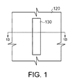
図2は、図1の線1B−1Bで切った断面図である。図1および図2において、半導体基板100が設けられている。一例では、基板100は単結晶シリコンである。基板100の上面105上に形成されているのは、埋め込み誘電体層であり、本例では、埋め込み酸化物層(BOX:buried oxide layer)110である。BOX110の上面115に形成されているのは、シリコン層120である。1つの例では、シリコン層120は、約200Åから2000Åの厚さである。シリコン層120は、単結晶シリコン、多結晶シリコン、またはアモルファス・シリコンとすることができる。基板100、BOX110、およびシリコン層120は、シリコン・オン・インシュレータ(SOI)基板またはSIMOX基板として取得することができる。シリコン層の上面125上に、エッチ・マスク130を形成する。一例では、エッチ・マスク130は、シリコン層120の上面125上にフォトレジスト層を塗布し、このフォトレジスト層をフォトリソグラフィによってパターニングすることによって形成する。
2 is a cross-sectional view taken along
図4は、図3の線2B−2Bで切った断面図である。図3および図4では、(例えばCF4を用いた)反応性イオン・エッチ(RIE)プロセスを行って、BOX110の上のシリコン層120から不要のシリコンが除去され、フィン135が残っている。フィン135は、幅Wおよび高さHを有する。高さHは、図2のシリコン層120の厚さと同じであり、約500Åから2000Åである。一例では、Wは、約50Åから350Åである。フィン135の基部表面140は、BOX110の上面115と直接物理的に接触し、このフィンとBOXとの間の接触および付着によって、フィンを支持する。
4 is a cross-sectional view taken along
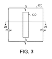
図6は、図5の線3B−3Bで切った断面図である。図5および図6では、緩衝フッ化水素酸(BHF:buffered hydrofluoric acid)を用いてマスク130(図4を参照)が除去され、フィン135の基部表面140の下にBOX110のアンダーカットが形成されている。この時点で、フィン135は基台145のみによって支持されている。図8は、図7の線4B−4Bで切った断面図である。図7および図8では、酸化およびBHF剥離を含む多数の洗浄ステップを行って、側壁150Aおよび150Bが洗浄され、側壁から結晶上の表面欠陥が除去されている。これらの洗浄ステップによって、フィン135の基部表面140の下にBOX110のアンダーカットがよりいっそう大きく形成される。フィン135は、この時点で、基台155のみによって支持されている。フィンのアンダーカットは、フィンの各側でDである。一例では、Dは約50Åから75Åである。フィン135を完全に切り取らないように注意しなければならない。フィン135の基部表面140と基台155との間の全接触面積が小さくなると、フィンは外れやすくなる。
6 is a cross-sectional view taken along line 3B-3B in FIG. 5 and 6, the mask 130 (see FIG. 4) is removed using buffered hydrofluoric acid (BHF), and an undercut of the
図10は、図9の線5B−5Bで切った断面図である。図9および図10では、フィン135の側壁150Aおよび150Bおよび上面150C、ならびにBOX110の露出した上面115を覆うように、コンフォーマルな(conformal)保護層160が形成されている。保護層160は、フィン135の側壁150Aおよび150Bを、以降の処理(以下で述べる)による潜在的な損傷から保護し、構造的にフィンを支持する。第1の例では、保護層160は、プラズマ・エンハンス化学気相付着(PECVD:plasma-enhanced chemical vapor deposition)によって形成した酸化テトラエトキシシラン(TEOS:tetraethoxysilane)であり、約15Åから50Åの厚さである。第2の例では、保護層160は、低圧化学気相付着(LPCVD:low-pressure chemical vapor deposition)によって形成した窒化シリコンであり、約15Åから50Åの厚さである。
10 is a cross-sectional view taken along
次に、ソース/ドレイン(S/D)領域等のドーピング領域を形成し、フィン135内のチャネル領域のドーピング・レベルを調整するために必要な一連のプロセス・ステップを行う。これらのステップは、各々、(1)フィン135の領域をフォトレジスト・マスクでマスクする、(2)イオン注入を行う、(3)(通常は酸素プラズマにおいて)フォトレジスト・マスクを除去する、および(4)任意のアニーリングを行う、ことを含む。これらの4つのステップを、2回から4回またはそれ以上繰り返すことができる。その正確な回数は、必要なフィン135内のドーパント・レベル制御に依存する。最後に、希釈フッ化水素酸(HF)洗浄、あるいはフアング(Huang)A洗浄、あるいはフアング(Huang)B洗浄、またはそれら全て等の洗浄を行う。イオン注入ステップの一例を、図11および図12に示し、以下で説明する。保護層160が所定の位置になければ、側壁150Aおよび150Bの表面に損傷を与える恐れがあり、フィン135はBOX110から外れるまで下部がえぐられることがある。
Next, a doped region, such as a source / drain (S / D) region, is formed and a series of process steps necessary to adjust the doping level of the channel region in the
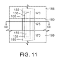
図12は、図11の線6B−6Bで切った断面図である。図11および図12では、フィン135のS/D領域170を覆うようにフォトレジスト・マスク165が形成され、フィンのチャネル領域175においてイオン注入が行われている。イオン注入種Xは、B、P、As、およびGe等の一般的に注入されるいずれかの種とすれば良い。ソース/ドレインのイオン注入では、チャネル領域175をマスクし、S/D領域170内に注入を行う。
12 is a cross-sectional view taken along
図14は、図13の線7B−7Bで切った断面図である。図13および図14では、保護層160およびBOX層110の部分を覆うように、フォトレジスト・マスク180を形成し、このフォトレジスト・マスクによって保護されていない場所で、フィン135から保護層を除去する。保護層160が窒化シリコンを含む例では、フッ素を用いたRIEまたはホット・リン酸エッチングを行うことができる。保護層160が二酸化シリコンを含む例では、フッ素を用いたRIEまたは希釈HF酸エッチングを行うことができる。
14 is a cross-sectional view taken along line 7B-7B in FIG. In FIGS. 13 and 14, a
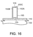
図16は、図15の線8B−8Bで切った断面図である。図15および図16では、フィン135の露出した側壁150Aおよび150Bならびに上面150Cの上に、ゲート誘電体層185が形成されている。一例では、ゲート誘電体層185は熱酸化物であり、約15Åから約50Åの厚さである。
16 is a cross-sectional view taken along
図18は、図17の線9B−9Bで切った断面図である。図17および図18では、フィンのチャネル領域175において、ゲート誘電体185およびフィン135を覆うようにゲート190が形成されている。本例では、ゲート190は、導電性材料のコンフォーマルな全面付着、フォトリソグラフィによるマスキング・ステップ、およびRIEによって形成される。適切なゲート材料の例には、ドーピングしたポリシリコン、ドーピングしていないポリシリコン、およびWまたはAl等の金属が含まれる。ゲート190は、フィン135の両側壁150Aおよび150Bを覆うように形成されるので、結果として得られるフィン型FETは二重ゲートになる。
18 is a cross-sectional view taken along
図20は、図19の線10B−10Bで切った断面図である。図19および図20では、保護層160が窒化シリコンである場合、希釈HFエッチングまたはフッ素を用いたRIEまたはH3PO4を用いて、いずれかの残った保護層160(図17を参照)が除去されている。ここで、フィン135は、フィン型FET構造の全体を覆うようにILDを付着するまで、ゲート190によって支持されている。
20 is a cross-sectional view taken along
図21は、ILDを形成した後の、図19および図20に示すようにコンフォーマルなゲートを利用したフィン型FETの断面図である。図21において、ILD層195は、ゲート190、フィン135の露出表面、およびBOX110の露出表面上に付着されている。化学−機械研磨(CMP:chemical-mechanical-polish)プロセスを行って、ILD層の上面200を平坦化する。ILD材料の例は、TEOS PECVD酸化物およびフッ素をドーピングしたガラス(FSG)を含んだ。結果として得られるフィン型FETは、ILD195に形成したバイアを介して、フィン135のS/D領域170(図11を参照)およびゲート190にコンタクトを形成することによって完了する。
FIG. 21 is a cross-sectional view of a fin-type FET using a conformal gate as shown in FIGS. 19 and 20 after the ILD is formed. In FIG. 21, an
図22は、レベル間誘電体(ILD:interlevel dielectric)を形成した後のダマシン平坦化ゲートを利用したフィン型FETの断面図である。図22では、ILD195を最初に付着し、ゲート190Aをダマシン・プロセスによって形成する。ダマシン・プロセスにおいて、ILDを覆うように適用したマスキング層をフォトリソグラフィによりパターニングすることによってILDにトレンチを形成し、ILDの反応性イオン・エッチング(RIE)を行い、マスキング層を除去し、充分な厚さの導電性材料を付着してトレンチを充填し、CMPプロセスを行って、導電性材料およびILDの上面を共に平坦化する。図22において、ILD195の上面200は、ゲート190Aの上面205と同一平面である。ダマシン・ゲートでは、トレンチをエッチングした後にゲート誘電体185を形成する必要がある場合がある。結果として得られるフィン型FETは、ゲート190Aに直接コンタクトを形成し、ILD195に形成したバイアを介してフィン135のS/D領域170(図11を参照)にコンタクトを形成することによって完了する。
FIG. 22 is a cross-sectional view of a fin-type FET using a damascene planarization gate after forming an interlevel dielectric (ILD). In FIG. 22,
図23から図31の図番が奇数の図は、本発明の第2の実施形態によるフィン型FET構造体の製造を示す上面図であり、これらに対応する図24から図32の図番が偶数の図は断面図である。 The figures with odd numbers in FIGS. 23 to 31 are top views showing the manufacture of the fin-type FET structure according to the second embodiment of the present invention, and the corresponding figure numbers in FIGS. 24 to 32 are shown. Even figures are cross-sectional views.
図24は、図23の線12B−12Bで切った断面図である。第2の実施形態の開始点は、図9および図10を参照して上述した保護層160の付着の直後であり、図1から図7または図2から図8に示した全ての先行ステップを含む。図23および図24は、図9および図10とそれぞれ同じである。
24 is a cross-sectional view taken along
図26は、図25の線13B−13Bで切った断面図である。図25および図26では、保護層160(図24を参照)のRIEを行って、フィン135の側壁150Aおよび150Bの下部215Aおよび215B上に、支持スペーサ210Aおよび210Bをそれぞれ形成する。スペーサ210Aおよび210Bは、フィン135に構造的な支持を与える。
26 is a cross-sectional view taken along
次に、ソース/ドレイン(S/D)領域等のドーピング領域を形成し、フィン135内のチャネル領域を調整するために必要な一連のプロセス・ステップを行う。これらのステップは、各々、(1)フィン135の領域をフォトレジスト・マスクでマスクする、(2)イオン注入を行う、(3)(通常は酸素プラズマにおいて)フォトレジスト・マスクを除去する、および(4)任意のアニーリングを行う、ことを含む。これらの4つのステップを、2回から4回またはそれ以上繰り返すことができる。その正確な回数は、必要なフィン135内のドーパント・レベル制御に依存する。最後に、希釈フッ化水素酸(HF)洗浄、あるいはフアング(Huang)A洗浄、あるいはフアング(Huang)B洗浄、またはそれら全て等の洗浄を行う。イオン注入ステップの一例を図27および図28に示し、以下に述べる。
Next, a doping region such as a source / drain (S / D) region is formed and a series of process steps necessary to adjust the channel region in the
図28は、図27の線14B−14Bで切った断面図である。図27および図28では、フィン135のS/D領域170を覆うようにフォトレジスト・マスク165が形成され、フィンのチャネル領域175にイオン注入が行われている。イオン注入種Xは、B、P、As、およびGe等の一般的に注入されるいずれかの種とすれば良い。ソース/ドレインのイオン注入では、チャネル領域175をマスクし、S/D領域170内に注入を行う。
28 is a cross-sectional view taken along
図30は、図29の線15B−15Bで切った断面図である。図29および図30では、フィン135の露出側壁150Aおよび150Bならびに上面150C上に、ゲート誘電体層185が形成されている。一例では、ゲート誘電体層185は熱酸化物であり、約15Åから50Åの厚さである。スペーサ210Aおよび210Bは、完成したフィン型FETデバイス中に組み込まれる。あるいは、ゲート誘電体185を形成する前に、支持スペーサ210Aおよび210Bを最初にRIEによって除去することも可能である。
30 is a cross-sectional view taken along
図32は、図31の線16B−16Bで切った断面図である。図31および図32では、フィンのチャネル領域175において、ゲート誘電体185およびフィン135を覆うようにゲート190が形成されている。本例では、ゲート190は、導電性材料のコンフォーマルな全面付着、フォトリソグラフィによるマスキング・ステップ、およびRIEによって形成する。適切なゲート材料の例には、ドーピングしたポリシリコン、ドーピングしていないポリシリコン、およびWまたはAl等の金属が含まれる。ゲート190は、フィン135の両側壁150Aおよび150Bを覆うように形成されるので、結果として得られるフィン型FETは二重ゲートになる。フィン型FETは、本発明の第1の実施形態について上述したように完成させることができる。
32 is a cross-sectional view taken along
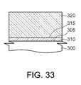
図33から図38は、本発明の第3の実施形態によるフィン型FET構造体の製造を示す断面図である。図33において、半導体基板300が設けられている。基板300の上面305上に形成されているのは、BOX310である。BOX310の上面315に形成されているのは、マンドレル層(mandrel layer)320である。1つの例では、マンドレル層320は窒化シリコンである。図34では、マンドレル層320(図33を参照)がフォトリソグラフィによってパターニングされ、RIEを行って、マンドレル325が形成されている。図35では、マンドレル325の上面335、側壁340、およびBOX310の露出上面315上に、アモルファス・シリコンまたは多結晶シリコン層330がコンフォーマルに付着されている。一例では、シリコン層330は、シリコンをスパッタリングすることによって形成する。シリコン層330に高温アニーリングを行って、これを単結晶シリコン層に変換する。図36では、シリコン層330(図35を参照)にRIEを行って、フィン345が形成されている。フィン345の内部側壁350Aは、マンドレル335の側壁340に接触している。図37では、マンドレル325の上面335、フィン345の上面360および外側側壁350B、ならびにBOX310の露出上面315を覆うように、コンフォーマルな保護層350が形成されている。図38では、RIEプロセスを行って、フィン345の外側側壁350Aの下部370に接触して支持スペーサ360が形成されている。上述のような更に別の処理を行って、フィン型FETデバイスを完成させることができる。支持スペーサ365は、処理の後の時点で除去するか、または所定の位置に残し、完成したフィン型FETデバイス内に組み込むことができる。
33 to 38 are cross-sectional views illustrating the manufacture of a fin-type FET structure according to the third embodiment of the present invention. In FIG. 33, a
従って、本発明は、結晶上、完璧に近く、薄いフィンに固有の構造的な弱さを克服した側壁表面を有する極めて薄いフィンを有するフィン型FETを製造する方法を開示する。 Accordingly, the present invention discloses a method of fabricating a fin-type FET having a very thin fin with a sidewall surface that is nearly perfect on the crystal and overcomes the structural weakness inherent in thin fins.
本発明の実施形態の説明は、本発明の理解のために与えられている。本発明は、本明細書中に記載した特定の実施形態に限定されず、本発明の範囲から逸脱することなく、現時点で当業者に明らかになる様々な変形、配置換え、および置換を行うことができることは理解されよう。従って、特許請求の範囲は、本発明の真の趣旨および範囲内に該当する全てのかかる変形および変更を包含することが意図される。 The description of the embodiments of the present invention is given for the understanding of the present invention. The present invention is not limited to the specific embodiments described herein, and various modifications, rearrangements, and substitutions that are now apparent to those skilled in the art can be made without departing from the scope of the invention. You will understand that you can. Accordingly, the claims are intended to cover all such modifications and changes as fall within the true spirit and scope of this invention.
Claims (17)
(a)半導体基板を設けるステップと、
(b)前記基板の上面上に誘電体層を形成するステップと、
(c)前記誘電体層の上面上にシリコン・フィンを形成するステップと、
(d)前記フィンの少なくとも1つの側壁上に保護層を形成するステップと、
(e)前記フィンのチャネル領域において、前記少なくとも1つの側壁から前記保護層を除去するステップと、
を含み、
ステップ(c)が、
前記誘電体層の前記上面上にシリコン層を形成するステップと、
前記シリコン層を覆うようにマスクを形成するステップと、
前記マスクによって保護されていない前記シリコン層の部分を除去して前記誘電体層を露出させるステップと、
前記マスクを除去するステップと、
を含み、
ステップ(c)とステップ(d)との間に、前記フィンの下から前記誘電体層の一部を除去するステップを更に含み、
ステップ(d)では、前記保護層は前記誘電体層の一部を除去した前記フィンの下にも形成される、
前記方法。A method of forming a fin-type FET device, comprising:
(A) providing a semiconductor substrate;
(B) forming a dielectric layer on the top surface of the substrate;
(C) forming silicon fins on the top surface of the dielectric layer;
(D) forming a protective layer on at least one sidewall of the fin;
(E) removing the protective layer from the at least one sidewall in the channel region of the fin;
Only including,
Step (c)
Forming a silicon layer on the top surface of the dielectric layer;
Forming a mask so as to cover the silicon layer;
Removing a portion of the silicon layer that is not protected by the mask to expose the dielectric layer;
Removing the mask;
Including
Further comprising removing a portion of the dielectric layer from under the fin between step (c) and step (d);
In step (d), the protective layer is also formed under the fin from which a part of the dielectric layer is removed.
Said method.
(g)前記ゲート誘電体上に導電性ゲートを形成するステップと、
を更に含む、請求項1に記載の方法。(F) forming a gate dielectric on the exposed surface of the fin in the channel region;
(G) forming a conductive gate on the gate dielectric;
The method of claim 1, further comprising:
(a)半導体基板を設けるステップと、
(b)前記基板の上面上に誘電体層を形成するステップと、
(c)前記誘電体層の上面上に側壁を有するシリコン・フィンを形成するステップと、
(d)前記側壁の少なくとも1つの少なくとも下部に保護層を形成するステップと、
を含み、
ステップ(c)が、
前記誘電体層の前記上面上にシリコン層を形成するステップと、
前記シリコン層を覆うようにマスクを形成するステップと、
前記マスクによって保護されていない前記シリコン層の部分を除去して前記誘電体層を露出させるステップと、
前記マスクを除去するステップと、
を含み、
ステップ(c)とステップ(d)との間に、前記フィンの下から前記誘電体層の一部を除去するステップを更に含み、
ステップ(d)では、前記保護層は前記誘電体層の一部を除去した前記フィンの下にも形成される、
前記方法。A method of forming a fin-type FET device, comprising:
(A) providing a semiconductor substrate;
(B) forming a dielectric layer on the top surface of the substrate;
(C) forming silicon fins having sidewalls on the top surface of the dielectric layer;
(D) forming a protective layer on at least the lower part of at least one of the side walls;
Only including,
Step (c)
Forming a silicon layer on the top surface of the dielectric layer;
Forming a mask so as to cover the silicon layer;
Removing a portion of the silicon layer that is not protected by the mask to expose the dielectric layer;
Removing the mask;
Including
Further comprising removing a portion of the dielectric layer from under the fin between step (c) and step (d);
In step (d), the protective layer is also formed under the fin from which a part of the dielectric layer is removed.
Said method.
(f)前記ゲート誘電体上に導電性ゲートを形成するステップと、
を更に含む、請求項5に記載の方法。(E) forming a gate dielectric on the exposed surface of the fin at least in a channel region of the fin;
(F) forming a conductive gate on the gate dielectric;
The method of claim 5 further comprising:
半導体基板と、
前記基板の上面上の誘電体層であって、厚い部分の基台を有する該誘電体層と、
前記誘電体層の前記基台の上の、側壁を有するシリコン・フィンであって、該シリコン・フィンの下に前記誘電体層のアンダーカットが形成されている該シリコン・フィンと、
前記フィンにおけるチャネル領域および該チャネル領域の両側のソース/ドレイン領域と、
前記チャネル領域において前記側壁の上部に接したゲート誘電体と、
前記側壁の少なくとも1つの少なくとも下部に接して、前記フィンの下では前記誘電体層の前記アンダーカットにまで入った保護層と、
前記チャネル領域において前記ゲート誘電体および前記保護層に接した導電性ゲートと、
を含む、フィン型FETデバイス。A fin-type FET device,
A semiconductor substrate;
A dielectric layer on an upper surface of the substrate, the dielectric layer having a thick base ;
A silicon fin having sidewalls on the base of the dielectric layer, the undercut of the dielectric layer being formed under the silicon fin ;
A channel region in the fin and source / drain regions on both sides of the channel region;
A gate dielectric in contact with the top of the sidewall in the channel region;
A protective layer in contact with at least the lower part of at least one of the side walls and under the fins and extending into the undercut of the dielectric layer;
A conductive gate in contact with the gate dielectric and the protective layer in the channel region;
A fin-type FET device.
Applications Claiming Priority (3)
| Application Number | Priority Date | Filing Date | Title |
|---|---|---|---|
| US10/605,905 US6962843B2 (en) | 2003-11-05 | 2003-11-05 | Method of fabricating a finfet |
| US10/605,905 | 2003-11-05 | ||
| PCT/US2004/037029 WO2005045900A2 (en) | 2003-11-05 | 2004-11-05 | Method of fabricating a finfet |
Publications (3)
| Publication Number | Publication Date |
|---|---|
| JP2007511077A JP2007511077A (en) | 2007-04-26 |
| JP2007511077A5 JP2007511077A5 (en) | 2007-11-29 |
| JP4953820B2 true JP4953820B2 (en) | 2012-06-13 |
Family
ID=34549689
Family Applications (1)
| Application Number | Title | Priority Date | Filing Date |
|---|---|---|---|
| JP2006538523A Expired - Fee Related JP4953820B2 (en) | 2003-11-05 | 2004-11-05 | Method for manufacturing fin-type FET |
Country Status (6)
| Country | Link |
|---|---|
| US (2) | US6962843B2 (en) |
| EP (1) | EP1690294A4 (en) |
| JP (1) | JP4953820B2 (en) |
| KR (1) | KR100843488B1 (en) |
| CN (1) | CN100459126C (en) |
| WO (1) | WO2005045900A2 (en) |
Families Citing this family (229)
| Publication number | Priority date | Publication date | Assignee | Title |
|---|---|---|---|---|
| US7087506B2 (en) * | 2003-06-26 | 2006-08-08 | International Business Machines Corporation | Method of forming freestanding semiconductor layer |
| US7049662B2 (en) * | 2003-11-26 | 2006-05-23 | International Business Machines Corporation | Structure and method to fabricate FinFET devices |
| US7352025B2 (en) * | 2003-12-08 | 2008-04-01 | International Business Machines Corporation | Semiconductor memory device with increased node capacitance |
| US7084018B1 (en) * | 2004-05-05 | 2006-08-01 | Advanced Micro Devices, Inc. | Sacrificial oxide for minimizing box undercut in damascene FinFET |
| JP3964885B2 (en) * | 2004-05-19 | 2007-08-22 | 株式会社東芝 | Semiconductor device and manufacturing method thereof |
| KR100591770B1 (en) * | 2004-09-01 | 2006-06-26 | 삼성전자주식회사 | Flash memory device using a semiconductor fin and method for fabricating the same |
| US7101763B1 (en) * | 2005-05-17 | 2006-09-05 | International Business Machines Corporation | Low capacitance junction-isolation for bulk FinFET technology |
| KR100645065B1 (en) * | 2005-06-23 | 2006-11-10 | 삼성전자주식회사 | Fin fet and non-volatile memory device having the same and method of forming the same |
| KR100642384B1 (en) * | 2005-09-15 | 2006-11-03 | 주식회사 하이닉스반도체 | Transistor for semiconductor memory device and method of fabricating the same |
| US7564081B2 (en) | 2005-11-30 | 2009-07-21 | International Business Machines Corporation | finFET structure with multiply stressed gate electrode |
| KR100838378B1 (en) * | 2006-09-29 | 2008-06-13 | 주식회사 하이닉스반도체 | Method for fabricating fin transistor |
| US7452758B2 (en) * | 2007-03-14 | 2008-11-18 | International Business Machines Corporation | Process for making FinFET device with body contact and buried oxide junction isolation |
| US7910482B2 (en) * | 2008-05-30 | 2011-03-22 | Freescale Semiconductor, Inc. | Method of forming a finFET and structure |
| US7863136B2 (en) * | 2008-09-30 | 2011-01-04 | Qimonda Ag | Method of manufacturing integrated circuits including a FET with a gate spacer and a fin |
| US8362482B2 (en) | 2009-04-14 | 2013-01-29 | Monolithic 3D Inc. | Semiconductor device and structure |
| US8405420B2 (en) | 2009-04-14 | 2013-03-26 | Monolithic 3D Inc. | System comprising a semiconductor device and structure |
| US8427200B2 (en) | 2009-04-14 | 2013-04-23 | Monolithic 3D Inc. | 3D semiconductor device |
| US8362800B2 (en) | 2010-10-13 | 2013-01-29 | Monolithic 3D Inc. | 3D semiconductor device including field repairable logics |
| US9509313B2 (en) | 2009-04-14 | 2016-11-29 | Monolithic 3D Inc. | 3D semiconductor device |
| US8395191B2 (en) | 2009-10-12 | 2013-03-12 | Monolithic 3D Inc. | Semiconductor device and structure |
| US8378715B2 (en) | 2009-04-14 | 2013-02-19 | Monolithic 3D Inc. | Method to construct systems |
| US8384426B2 (en) | 2009-04-14 | 2013-02-26 | Monolithic 3D Inc. | Semiconductor device and structure |
| US8258810B2 (en) | 2010-09-30 | 2012-09-04 | Monolithic 3D Inc. | 3D semiconductor device |
| US8669778B1 (en) | 2009-04-14 | 2014-03-11 | Monolithic 3D Inc. | Method for design and manufacturing of a 3D semiconductor device |
| US8058137B1 (en) | 2009-04-14 | 2011-11-15 | Monolithic 3D Inc. | Method for fabrication of a semiconductor device and structure |
| US7986042B2 (en) | 2009-04-14 | 2011-07-26 | Monolithic 3D Inc. | Method for fabrication of a semiconductor device and structure |
| US9577642B2 (en) | 2009-04-14 | 2017-02-21 | Monolithic 3D Inc. | Method to form a 3D semiconductor device |
| US8754533B2 (en) | 2009-04-14 | 2014-06-17 | Monolithic 3D Inc. | Monolithic three-dimensional semiconductor device and structure |
| US8373439B2 (en) | 2009-04-14 | 2013-02-12 | Monolithic 3D Inc. | 3D semiconductor device |
| US9711407B2 (en) | 2009-04-14 | 2017-07-18 | Monolithic 3D Inc. | Method of manufacturing a three dimensional integrated circuit by transfer of a mono-crystalline layer |
| US20100308440A1 (en) * | 2009-06-08 | 2010-12-09 | Globalfoundries Inc. | Semiconductor structures and methods for stabilizing silicon-comprising structures on a silicon oxide layer of a semiconductor substrate |
| US8124507B2 (en) * | 2009-06-24 | 2012-02-28 | Panasonic Corporation | Semiconductor device and method for fabricating the same |
| US8742476B1 (en) | 2012-11-27 | 2014-06-03 | Monolithic 3D Inc. | Semiconductor device and structure |
| US8294159B2 (en) | 2009-10-12 | 2012-10-23 | Monolithic 3D Inc. | Method for fabrication of a semiconductor device and structure |
| US9099424B1 (en) | 2012-08-10 | 2015-08-04 | Monolithic 3D Inc. | Semiconductor system, device and structure with heat removal |
| US8476145B2 (en) | 2010-10-13 | 2013-07-02 | Monolithic 3D Inc. | Method of fabricating a semiconductor device and structure |
| US11374118B2 (en) | 2009-10-12 | 2022-06-28 | Monolithic 3D Inc. | Method to form a 3D integrated circuit |
| US8581349B1 (en) | 2011-05-02 | 2013-11-12 | Monolithic 3D Inc. | 3D memory semiconductor device and structure |
| US10043781B2 (en) | 2009-10-12 | 2018-08-07 | Monolithic 3D Inc. | 3D semiconductor device and structure |
| US10157909B2 (en) | 2009-10-12 | 2018-12-18 | Monolithic 3D Inc. | 3D semiconductor device and structure |
| US10366970B2 (en) | 2009-10-12 | 2019-07-30 | Monolithic 3D Inc. | 3D semiconductor device and structure |
| US8450804B2 (en) | 2011-03-06 | 2013-05-28 | Monolithic 3D Inc. | Semiconductor device and structure for heat removal |
| US8536023B2 (en) | 2010-11-22 | 2013-09-17 | Monolithic 3D Inc. | Method of manufacturing a semiconductor device and structure |
| US10354995B2 (en) | 2009-10-12 | 2019-07-16 | Monolithic 3D Inc. | Semiconductor memory device and structure |
| US10388863B2 (en) | 2009-10-12 | 2019-08-20 | Monolithic 3D Inc. | 3D memory device and structure |
| US11018133B2 (en) | 2009-10-12 | 2021-05-25 | Monolithic 3D Inc. | 3D integrated circuit |
| US10910364B2 (en) | 2009-10-12 | 2021-02-02 | Monolitaic 3D Inc. | 3D semiconductor device |
| US9099526B2 (en) | 2010-02-16 | 2015-08-04 | Monolithic 3D Inc. | Integrated circuit device and structure |
| US8492886B2 (en) | 2010-02-16 | 2013-07-23 | Monolithic 3D Inc | 3D integrated circuit with logic |
| US8026521B1 (en) | 2010-10-11 | 2011-09-27 | Monolithic 3D Inc. | Semiconductor device and structure |
| US8541819B1 (en) | 2010-12-09 | 2013-09-24 | Monolithic 3D Inc. | Semiconductor device and structure |
| US8373230B1 (en) | 2010-10-13 | 2013-02-12 | Monolithic 3D Inc. | Method for fabrication of a semiconductor device and structure |
| US8461035B1 (en) | 2010-09-30 | 2013-06-11 | Monolithic 3D Inc. | Method for fabrication of a semiconductor device and structure |
| US8298875B1 (en) | 2011-03-06 | 2012-10-30 | Monolithic 3D Inc. | Method for fabrication of a semiconductor device and structure |
| CN102315224B (en) * | 2010-07-07 | 2014-01-15 | 中国科学院微电子研究所 | Nonvolatile storage device making using of Fin FET (Field Effect Transistor) and manufacturing method thereof |
| US8338256B2 (en) | 2010-07-08 | 2012-12-25 | International Business Machines Corporation | Multi-gate transistor having sidewall contacts |
| US10217667B2 (en) | 2011-06-28 | 2019-02-26 | Monolithic 3D Inc. | 3D semiconductor device, fabrication method and system |
| US8642416B2 (en) | 2010-07-30 | 2014-02-04 | Monolithic 3D Inc. | Method of forming three dimensional integrated circuit devices using layer transfer technique |
| US9953925B2 (en) | 2011-06-28 | 2018-04-24 | Monolithic 3D Inc. | Semiconductor system and device |
| US8901613B2 (en) | 2011-03-06 | 2014-12-02 | Monolithic 3D Inc. | Semiconductor device and structure for heat removal |
| US9219005B2 (en) | 2011-06-28 | 2015-12-22 | Monolithic 3D Inc. | Semiconductor system and device |
| US11482440B2 (en) | 2010-12-16 | 2022-10-25 | Monolithic 3D Inc. | 3D semiconductor device and structure with a built-in test circuit for repairing faulty circuits |
| US8273610B2 (en) | 2010-11-18 | 2012-09-25 | Monolithic 3D Inc. | Method of constructing a semiconductor device and structure |
| US10497713B2 (en) | 2010-11-18 | 2019-12-03 | Monolithic 3D Inc. | 3D semiconductor memory device and structure |
| US8163581B1 (en) | 2010-10-13 | 2012-04-24 | Monolith IC 3D | Semiconductor and optoelectronic devices |
| US8114757B1 (en) | 2010-10-11 | 2012-02-14 | Monolithic 3D Inc. | Semiconductor device and structure |
| US11227897B2 (en) | 2010-10-11 | 2022-01-18 | Monolithic 3D Inc. | Method for producing a 3D semiconductor memory device and structure |
| US11315980B1 (en) | 2010-10-11 | 2022-04-26 | Monolithic 3D Inc. | 3D semiconductor device and structure with transistors |
| US11469271B2 (en) | 2010-10-11 | 2022-10-11 | Monolithic 3D Inc. | Method to produce 3D semiconductor devices and structures with memory |
| US10290682B2 (en) | 2010-10-11 | 2019-05-14 | Monolithic 3D Inc. | 3D IC semiconductor device and structure with stacked memory |
| US11158674B2 (en) | 2010-10-11 | 2021-10-26 | Monolithic 3D Inc. | Method to produce a 3D semiconductor device and structure |
| US11257867B1 (en) | 2010-10-11 | 2022-02-22 | Monolithic 3D Inc. | 3D semiconductor device and structure with oxide bonds |
| US11024673B1 (en) | 2010-10-11 | 2021-06-01 | Monolithic 3D Inc. | 3D semiconductor device and structure |
| US11600667B1 (en) | 2010-10-11 | 2023-03-07 | Monolithic 3D Inc. | Method to produce 3D semiconductor devices and structures with memory |
| US11018191B1 (en) | 2010-10-11 | 2021-05-25 | Monolithic 3D Inc. | 3D semiconductor device and structure |
| US10896931B1 (en) | 2010-10-11 | 2021-01-19 | Monolithic 3D Inc. | 3D semiconductor device and structure |
| US9197804B1 (en) | 2011-10-14 | 2015-11-24 | Monolithic 3D Inc. | Semiconductor and optoelectronic devices |
| US11404466B2 (en) | 2010-10-13 | 2022-08-02 | Monolithic 3D Inc. | Multilevel semiconductor device and structure with image sensors |
| US11437368B2 (en) | 2010-10-13 | 2022-09-06 | Monolithic 3D Inc. | Multilevel semiconductor device and structure with oxide bonding |
| US11869915B2 (en) | 2010-10-13 | 2024-01-09 | Monolithic 3D Inc. | Multilevel semiconductor device and structure with image sensors and wafer bonding |
| US11133344B2 (en) | 2010-10-13 | 2021-09-28 | Monolithic 3D Inc. | Multilevel semiconductor device and structure with image sensors |
| US10943934B2 (en) | 2010-10-13 | 2021-03-09 | Monolithic 3D Inc. | Multilevel semiconductor device and structure |
| US10833108B2 (en) | 2010-10-13 | 2020-11-10 | Monolithic 3D Inc. | 3D microdisplay device and structure |
| US10978501B1 (en) | 2010-10-13 | 2021-04-13 | Monolithic 3D Inc. | Multilevel semiconductor device and structure with waveguides |
| US11694922B2 (en) | 2010-10-13 | 2023-07-04 | Monolithic 3D Inc. | Multilevel semiconductor device and structure with oxide bonding |
| US11063071B1 (en) | 2010-10-13 | 2021-07-13 | Monolithic 3D Inc. | Multilevel semiconductor device and structure with waveguides |
| US11163112B2 (en) | 2010-10-13 | 2021-11-02 | Monolithic 3D Inc. | Multilevel semiconductor device and structure with electromagnetic modulators |
| US8283215B2 (en) | 2010-10-13 | 2012-10-09 | Monolithic 3D Inc. | Semiconductor and optoelectronic devices |
| US11043523B1 (en) | 2010-10-13 | 2021-06-22 | Monolithic 3D Inc. | Multilevel semiconductor device and structure with image sensors |
| US10679977B2 (en) | 2010-10-13 | 2020-06-09 | Monolithic 3D Inc. | 3D microdisplay device and structure |
| US10998374B1 (en) | 2010-10-13 | 2021-05-04 | Monolithic 3D Inc. | Multilevel semiconductor device and structure |
| US11855100B2 (en) | 2010-10-13 | 2023-12-26 | Monolithic 3D Inc. | Multilevel semiconductor device and structure with oxide bonding |
| US11855114B2 (en) | 2010-10-13 | 2023-12-26 | Monolithic 3D Inc. | Multilevel semiconductor device and structure with image sensors and wafer bonding |
| US11164898B2 (en) | 2010-10-13 | 2021-11-02 | Monolithic 3D Inc. | Multilevel semiconductor device and structure |
| US11327227B2 (en) | 2010-10-13 | 2022-05-10 | Monolithic 3D Inc. | Multilevel semiconductor device and structure with electromagnetic modulators |
| US11929372B2 (en) | 2010-10-13 | 2024-03-12 | Monolithic 3D Inc. | Multilevel semiconductor device and structure with image sensors and wafer bonding |
| US8379458B1 (en) | 2010-10-13 | 2013-02-19 | Monolithic 3D Inc. | Semiconductor device and structure |
| US11605663B2 (en) | 2010-10-13 | 2023-03-14 | Monolithic 3D Inc. | Multilevel semiconductor device and structure with image sensors and wafer bonding |
| US8211759B2 (en) | 2010-10-21 | 2012-07-03 | International Business Machines Corporation | Semiconductor structure and methods of manufacture |
| US8232164B2 (en) | 2010-10-29 | 2012-07-31 | International Business Machines Corporation | Damascene method of forming a semiconductor structure and a semiconductor structure with multiple fin-shaped channel regions having different widths |
| US11735462B2 (en) | 2010-11-18 | 2023-08-22 | Monolithic 3D Inc. | 3D semiconductor device and structure with single-crystal layers |
| US11211279B2 (en) | 2010-11-18 | 2021-12-28 | Monolithic 3D Inc. | Method for processing a 3D integrated circuit and structure |
| US11508605B2 (en) | 2010-11-18 | 2022-11-22 | Monolithic 3D Inc. | 3D semiconductor memory device and structure |
| US11854857B1 (en) | 2010-11-18 | 2023-12-26 | Monolithic 3D Inc. | Methods for producing a 3D semiconductor device and structure with memory cells and multiple metal layers |
| US11443971B2 (en) | 2010-11-18 | 2022-09-13 | Monolithic 3D Inc. | 3D semiconductor device and structure with memory |
| US11569117B2 (en) | 2010-11-18 | 2023-01-31 | Monolithic 3D Inc. | 3D semiconductor device and structure with single-crystal layers |
| US11355380B2 (en) | 2010-11-18 | 2022-06-07 | Monolithic 3D Inc. | Methods for producing 3D semiconductor memory device and structure utilizing alignment marks |
| US11482438B2 (en) | 2010-11-18 | 2022-10-25 | Monolithic 3D Inc. | Methods for producing a 3D semiconductor memory device and structure |
| US11901210B2 (en) | 2010-11-18 | 2024-02-13 | Monolithic 3D Inc. | 3D semiconductor device and structure with memory |
| US11482439B2 (en) | 2010-11-18 | 2022-10-25 | Monolithic 3D Inc. | Methods for producing a 3D semiconductor memory device comprising charge trap junction-less transistors |
| US11031275B2 (en) | 2010-11-18 | 2021-06-08 | Monolithic 3D Inc. | 3D semiconductor device and structure with memory |
| US11004719B1 (en) | 2010-11-18 | 2021-05-11 | Monolithic 3D Inc. | Methods for producing a 3D semiconductor memory device and structure |
| US11804396B2 (en) | 2010-11-18 | 2023-10-31 | Monolithic 3D Inc. | Methods for producing a 3D semiconductor device and structure with memory cells and multiple metal layers |
| US11094576B1 (en) | 2010-11-18 | 2021-08-17 | Monolithic 3D Inc. | Methods for producing a 3D semiconductor memory device and structure |
| US11121021B2 (en) | 2010-11-18 | 2021-09-14 | Monolithic 3D Inc. | 3D semiconductor device and structure |
| US11610802B2 (en) | 2010-11-18 | 2023-03-21 | Monolithic 3D Inc. | Method for producing a 3D semiconductor device and structure with single crystal transistors and metal gate electrodes |
| US11355381B2 (en) | 2010-11-18 | 2022-06-07 | Monolithic 3D Inc. | 3D semiconductor memory device and structure |
| US11018042B1 (en) | 2010-11-18 | 2021-05-25 | Monolithic 3D Inc. | 3D semiconductor memory device and structure |
| US11862503B2 (en) | 2010-11-18 | 2024-01-02 | Monolithic 3D Inc. | Method for producing a 3D semiconductor device and structure with memory cells and multiple metal layers |
| US11521888B2 (en) | 2010-11-18 | 2022-12-06 | Monolithic 3D Inc. | 3D semiconductor device and structure with high-k metal gate transistors |
| US11923230B1 (en) | 2010-11-18 | 2024-03-05 | Monolithic 3D Inc. | 3D semiconductor device and structure with bonding |
| US11615977B2 (en) | 2010-11-18 | 2023-03-28 | Monolithic 3D Inc. | 3D semiconductor memory device and structure |
| US11495484B2 (en) | 2010-11-18 | 2022-11-08 | Monolithic 3D Inc. | 3D semiconductor devices and structures with at least two single-crystal layers |
| US11164770B1 (en) | 2010-11-18 | 2021-11-02 | Monolithic 3D Inc. | Method for producing a 3D semiconductor memory device and structure |
| US11784082B2 (en) | 2010-11-18 | 2023-10-10 | Monolithic 3D Inc. | 3D semiconductor device and structure with bonding |
| US11107721B2 (en) | 2010-11-18 | 2021-08-31 | Monolithic 3D Inc. | 3D semiconductor device and structure with NAND logic |
| US8975670B2 (en) | 2011-03-06 | 2015-03-10 | Monolithic 3D Inc. | Semiconductor device and structure for heat removal |
| US9401436B2 (en) | 2011-05-05 | 2016-07-26 | Qualcomm Incorporated | Multiple control transcap variable capacitor |
| US10388568B2 (en) | 2011-06-28 | 2019-08-20 | Monolithic 3D Inc. | 3D semiconductor device and system |
| US8687399B2 (en) | 2011-10-02 | 2014-04-01 | Monolithic 3D Inc. | Semiconductor device and structure |
| US9029173B2 (en) | 2011-10-18 | 2015-05-12 | Monolithic 3D Inc. | Method for fabrication of a semiconductor device and structure |
| US8569125B2 (en) * | 2011-11-30 | 2013-10-29 | International Business Machines Corporation | FinFET with improved gate planarity |
| US9000557B2 (en) | 2012-03-17 | 2015-04-07 | Zvi Or-Bach | Semiconductor device and structure |
| US11616004B1 (en) | 2012-04-09 | 2023-03-28 | Monolithic 3D Inc. | 3D semiconductor device and structure with metal layers and a connective path |
| US11594473B2 (en) | 2012-04-09 | 2023-02-28 | Monolithic 3D Inc. | 3D semiconductor device and structure with metal layers and a connective path |
| US8557632B1 (en) | 2012-04-09 | 2013-10-15 | Monolithic 3D Inc. | Method for fabrication of a semiconductor device and structure |
| US11476181B1 (en) | 2012-04-09 | 2022-10-18 | Monolithic 3D Inc. | 3D semiconductor device and structure with metal layers |
| US11410912B2 (en) | 2012-04-09 | 2022-08-09 | Monolithic 3D Inc. | 3D semiconductor device with vias and isolation layers |
| US11088050B2 (en) | 2012-04-09 | 2021-08-10 | Monolithic 3D Inc. | 3D semiconductor device with isolation layers |
| US11881443B2 (en) | 2012-04-09 | 2024-01-23 | Monolithic 3D Inc. | 3D semiconductor device and structure with metal layers and a connective path |
| US11735501B1 (en) | 2012-04-09 | 2023-08-22 | Monolithic 3D Inc. | 3D semiconductor device and structure with metal layers and a connective path |
| US11164811B2 (en) | 2012-04-09 | 2021-11-02 | Monolithic 3D Inc. | 3D semiconductor device with isolation layers and oxide-to-oxide bonding |
| US10600888B2 (en) | 2012-04-09 | 2020-03-24 | Monolithic 3D Inc. | 3D semiconductor device |
| US11694944B1 (en) | 2012-04-09 | 2023-07-04 | Monolithic 3D Inc. | 3D semiconductor device and structure with metal layers and a connective path |
| CN103811344B (en) * | 2012-11-09 | 2016-08-10 | 中国科学院微电子研究所 | Semiconductor device and manufacture method thereof |
| US8686428B1 (en) | 2012-11-16 | 2014-04-01 | Monolithic 3D Inc. | Semiconductor device and structure |
| US8574929B1 (en) | 2012-11-16 | 2013-11-05 | Monolithic 3D Inc. | Method to form a 3D semiconductor device and structure |
| CN107863299B (en) * | 2012-11-30 | 2021-06-15 | 中国科学院微电子研究所 | FinFET and manufacturing method thereof |
| US11063024B1 (en) | 2012-12-22 | 2021-07-13 | Monlithic 3D Inc. | Method to form a 3D semiconductor device and structure |
| US11916045B2 (en) | 2012-12-22 | 2024-02-27 | Monolithic 3D Inc. | 3D semiconductor device and structure with metal layers |
| US8674470B1 (en) | 2012-12-22 | 2014-03-18 | Monolithic 3D Inc. | Semiconductor device and structure |
| US11018116B2 (en) | 2012-12-22 | 2021-05-25 | Monolithic 3D Inc. | Method to form a 3D semiconductor device and structure |
| US11784169B2 (en) | 2012-12-22 | 2023-10-10 | Monolithic 3D Inc. | 3D semiconductor device and structure with metal layers |
| US11309292B2 (en) | 2012-12-22 | 2022-04-19 | Monolithic 3D Inc. | 3D semiconductor device and structure with metal layers |
| US11217565B2 (en) | 2012-12-22 | 2022-01-04 | Monolithic 3D Inc. | Method to form a 3D semiconductor device and structure |
| US10115663B2 (en) | 2012-12-29 | 2018-10-30 | Monolithic 3D Inc. | 3D semiconductor device and structure |
| US9871034B1 (en) | 2012-12-29 | 2018-01-16 | Monolithic 3D Inc. | Semiconductor device and structure |
| US11430668B2 (en) | 2012-12-29 | 2022-08-30 | Monolithic 3D Inc. | 3D semiconductor device and structure with bonding |
| US11087995B1 (en) | 2012-12-29 | 2021-08-10 | Monolithic 3D Inc. | 3D semiconductor device and structure |
| US10600657B2 (en) | 2012-12-29 | 2020-03-24 | Monolithic 3D Inc | 3D semiconductor device and structure |
| US11430667B2 (en) | 2012-12-29 | 2022-08-30 | Monolithic 3D Inc. | 3D semiconductor device and structure with bonding |
| US10651054B2 (en) | 2012-12-29 | 2020-05-12 | Monolithic 3D Inc. | 3D semiconductor device and structure |
| US10903089B1 (en) | 2012-12-29 | 2021-01-26 | Monolithic 3D Inc. | 3D semiconductor device and structure |
| US11004694B1 (en) | 2012-12-29 | 2021-05-11 | Monolithic 3D Inc. | 3D semiconductor device and structure |
| US11177140B2 (en) | 2012-12-29 | 2021-11-16 | Monolithic 3D Inc. | 3D semiconductor device and structure |
| US10892169B2 (en) | 2012-12-29 | 2021-01-12 | Monolithic 3D Inc. | 3D semiconductor device and structure |
| US9385058B1 (en) | 2012-12-29 | 2016-07-05 | Monolithic 3D Inc. | Semiconductor device and structure |
| FR3002813B1 (en) | 2013-03-01 | 2016-08-05 | St Microelectronics Sa | METHOD FOR MANUFACTURING A MOS-TOILET TRANSISTOR |
| US11935949B1 (en) | 2013-03-11 | 2024-03-19 | Monolithic 3D Inc. | 3D semiconductor device and structure with metal layers and memory cells |
| US10325651B2 (en) | 2013-03-11 | 2019-06-18 | Monolithic 3D Inc. | 3D semiconductor device with stacked memory |
| US8902663B1 (en) | 2013-03-11 | 2014-12-02 | Monolithic 3D Inc. | Method of maintaining a memory state |
| US11869965B2 (en) | 2013-03-11 | 2024-01-09 | Monolithic 3D Inc. | 3D semiconductor device and structure with metal layers and memory cells |
| US11088130B2 (en) | 2014-01-28 | 2021-08-10 | Monolithic 3D Inc. | 3D semiconductor device and structure |
| US8994404B1 (en) | 2013-03-12 | 2015-03-31 | Monolithic 3D Inc. | Semiconductor device and structure |
| US11923374B2 (en) | 2013-03-12 | 2024-03-05 | Monolithic 3D Inc. | 3D semiconductor device and structure with metal layers |
| US11398569B2 (en) | 2013-03-12 | 2022-07-26 | Monolithic 3D Inc. | 3D semiconductor device and structure |
| US10840239B2 (en) | 2014-08-26 | 2020-11-17 | Monolithic 3D Inc. | 3D semiconductor device and structure |
| US9117749B1 (en) | 2013-03-15 | 2015-08-25 | Monolithic 3D Inc. | Semiconductor device and structure |
| US10224279B2 (en) | 2013-03-15 | 2019-03-05 | Monolithic 3D Inc. | Semiconductor device and structure |
| US11720736B2 (en) | 2013-04-15 | 2023-08-08 | Monolithic 3D Inc. | Automation methods for 3D integrated circuits and devices |
| US11030371B2 (en) | 2013-04-15 | 2021-06-08 | Monolithic 3D Inc. | Automation for monolithic 3D devices |
| US11341309B1 (en) | 2013-04-15 | 2022-05-24 | Monolithic 3D Inc. | Automation for monolithic 3D devices |
| US11487928B2 (en) | 2013-04-15 | 2022-11-01 | Monolithic 3D Inc. | Automation for monolithic 3D devices |
| US11574109B1 (en) | 2013-04-15 | 2023-02-07 | Monolithic 3D Inc | Automation methods for 3D integrated circuits and devices |
| US9021414B1 (en) | 2013-04-15 | 2015-04-28 | Monolithic 3D Inc. | Automation for monolithic 3D devices |
| US11270055B1 (en) | 2013-04-15 | 2022-03-08 | Monolithic 3D Inc. | Automation for monolithic 3D devices |
| US9306036B2 (en) * | 2013-07-30 | 2016-04-05 | Globalfoundries Inc. | Nitride spacer for protecting a fin-shaped field effect transistor (finFET) device |
| US9252272B2 (en) * | 2013-11-18 | 2016-02-02 | Globalfoundries Inc. | FinFET semiconductor device having local buried oxide |
| US9312273B2 (en) | 2013-12-02 | 2016-04-12 | International Business Machines Corporation | Structure and method to reduce crystal defects in epitaxial fin merge using nitride deposition |
| US9496282B2 (en) | 2013-12-02 | 2016-11-15 | International Business Machines Corporation | Structure and method to reduce crystal defects in epitaxial fin merge using nitride deposition |
| US11107808B1 (en) | 2014-01-28 | 2021-08-31 | Monolithic 3D Inc. | 3D semiconductor device and structure |
| US11031394B1 (en) | 2014-01-28 | 2021-06-08 | Monolithic 3D Inc. | 3D semiconductor device and structure |
| US10297586B2 (en) | 2015-03-09 | 2019-05-21 | Monolithic 3D Inc. | Methods for processing a 3D semiconductor device |
| US9214557B2 (en) * | 2014-02-06 | 2015-12-15 | Globalfoundries Singapore Pte. Ltd. | Device with isolation buffer |
| US9548213B2 (en) | 2014-02-25 | 2017-01-17 | International Business Machines Corporation | Dielectric isolated fin with improved fin profile |
| US9685501B2 (en) | 2014-04-02 | 2017-06-20 | International Business Machines Corporation | Low parasitic capacitance finFET device |
| US9530659B2 (en) | 2014-05-02 | 2016-12-27 | International Business Machines Corporation | Structure for preventing buried oxide gouging during planar and FinFET Processing on SOI |
| US9490346B2 (en) | 2014-06-12 | 2016-11-08 | Taiwan Semiconductor Manufacturing Co., Ltd. | Structure and formation method of fin-like field effect transistor |
| US9502538B2 (en) | 2014-06-12 | 2016-11-22 | Taiwan Semiconductor Manufacturing Co., Ltd | Structure and formation method of fin-like field effect transistor |
| US9490365B2 (en) | 2014-06-12 | 2016-11-08 | Taiwan Semiconductor Manufacturing Co., Ltd. | Structure and formation method of fin-like field effect transistor |
| US9478660B2 (en) | 2015-01-12 | 2016-10-25 | Taiwan Semiconductor Manufacturing Co., Ltd. | Protection layer on fin of fin field effect transistor (FinFET) device structure |
| US9496373B2 (en) * | 2015-04-02 | 2016-11-15 | International Business Machines Corporation | Damage-resistant fin structures and FinFET CMOS |
| US11011507B1 (en) | 2015-04-19 | 2021-05-18 | Monolithic 3D Inc. | 3D semiconductor device and structure |
| US11056468B1 (en) | 2015-04-19 | 2021-07-06 | Monolithic 3D Inc. | 3D semiconductor device and structure |
| US10825779B2 (en) | 2015-04-19 | 2020-11-03 | Monolithic 3D Inc. | 3D semiconductor device and structure |
| US10381328B2 (en) | 2015-04-19 | 2019-08-13 | Monolithic 3D Inc. | Semiconductor device and structure |
| CN108401468A (en) | 2015-09-21 | 2018-08-14 | 莫诺利特斯3D有限公司 | 3D semiconductor devices and structure |
| US10522225B1 (en) | 2015-10-02 | 2019-12-31 | Monolithic 3D Inc. | Semiconductor device with non-volatile memory |
| US11296115B1 (en) | 2015-10-24 | 2022-04-05 | Monolithic 3D Inc. | 3D semiconductor device and structure |
| US10418369B2 (en) | 2015-10-24 | 2019-09-17 | Monolithic 3D Inc. | Multi-level semiconductor memory device and structure |
| US11114464B2 (en) | 2015-10-24 | 2021-09-07 | Monolithic 3D Inc. | 3D semiconductor device and structure |
| US10847540B2 (en) | 2015-10-24 | 2020-11-24 | Monolithic 3D Inc. | 3D semiconductor memory device and structure |
| US11114427B2 (en) | 2015-11-07 | 2021-09-07 | Monolithic 3D Inc. | 3D semiconductor processor and memory device and structure |
| US11937422B2 (en) | 2015-11-07 | 2024-03-19 | Monolithic 3D Inc. | Semiconductor memory device and structure |
| US11930648B1 (en) | 2016-10-10 | 2024-03-12 | Monolithic 3D Inc. | 3D memory devices and structures with metal layers |
| US11251149B2 (en) | 2016-10-10 | 2022-02-15 | Monolithic 3D Inc. | 3D memory device and structure |
| US11812620B2 (en) | 2016-10-10 | 2023-11-07 | Monolithic 3D Inc. | 3D DRAM memory devices and structures with control circuits |
| US11329059B1 (en) | 2016-10-10 | 2022-05-10 | Monolithic 3D Inc. | 3D memory devices and structures with thinned single crystal substrates |
| US11711928B2 (en) | 2016-10-10 | 2023-07-25 | Monolithic 3D Inc. | 3D memory devices and structures with control circuits |
| US11869591B2 (en) | 2016-10-10 | 2024-01-09 | Monolithic 3D Inc. | 3D memory devices and structures with control circuits |
| US9997590B2 (en) * | 2016-10-24 | 2018-06-12 | International Büsiness Machines Corporation | FinFET resistor and method to fabricate same |
| TWI604569B (en) * | 2016-11-15 | 2017-11-01 | 新唐科技股份有限公司 | Semiconductor devices and methods for forming the same |
| US10374066B2 (en) | 2017-07-11 | 2019-08-06 | International Business Machines Corporation | Fin and shallow trench isolation replacement to prevent gate collapse |
| US11164876B2 (en) * | 2019-02-07 | 2021-11-02 | Micron Technology, Inc. | Atom implantation for passivation of pillar material |
| US10892016B1 (en) | 2019-04-08 | 2021-01-12 | Monolithic 3D Inc. | 3D memory semiconductor devices and structures |
| US11763864B2 (en) | 2019-04-08 | 2023-09-19 | Monolithic 3D Inc. | 3D memory semiconductor devices and structures with bit-line pillars |
| US11158652B1 (en) | 2019-04-08 | 2021-10-26 | Monolithic 3D Inc. | 3D memory semiconductor devices and structures |
| US11296106B2 (en) | 2019-04-08 | 2022-04-05 | Monolithic 3D Inc. | 3D memory semiconductor devices and structures |
| US11018156B2 (en) | 2019-04-08 | 2021-05-25 | Monolithic 3D Inc. | 3D memory semiconductor devices and structures |
Family Cites Families (34)
| Publication number | Priority date | Publication date | Assignee | Title |
|---|---|---|---|---|
| US4252574A (en) | 1979-11-09 | 1981-02-24 | Rca Corporation | Low leakage N-channel SOS transistors and method of making them |
| US4393572A (en) | 1980-05-29 | 1983-07-19 | Rca Corporation | Method of making low leakage N-channel SOS transistors utilizing positive photoresist masking techniques |
| US4714685A (en) | 1986-12-08 | 1987-12-22 | General Motors Corporation | Method of fabricating self-aligned silicon-on-insulator like devices |
| US4716128A (en) | 1986-12-10 | 1987-12-29 | General Motors Corporation | Method of fabricating silicon-on-insulator like devices |
| JPH01291465A (en) * | 1988-05-19 | 1989-11-24 | Fujitsu Ltd | Mis field-effect semiconductor device and manufacture thereof |
| US5346834A (en) | 1988-11-21 | 1994-09-13 | Hitachi, Ltd. | Method for manufacturing a semiconductor device and a semiconductor memory device |
| US6143582A (en) | 1990-12-31 | 2000-11-07 | Kopin Corporation | High density electronic circuit modules |
| US5391506A (en) | 1992-01-31 | 1995-02-21 | Kawasaki Steel Corporation | Manufacturing method for semiconductor devices with source/drain formed in substrate projection. |
| JPH08167721A (en) * | 1994-12-09 | 1996-06-25 | Lg Semicon Co Ltd | Structure of thin-film transistor and its manufacture |
| JPH08316348A (en) * | 1995-03-14 | 1996-11-29 | Toshiba Corp | Semiconductor device and fabrication thereof |
| JP3607431B2 (en) * | 1996-09-18 | 2005-01-05 | 株式会社東芝 | Semiconductor device and manufacturing method thereof |
| US6271095B1 (en) | 1999-02-22 | 2001-08-07 | Advanced Micro Devices, Inc. | Locally confined deep pocket process for ULSI mosfets |
| US6252284B1 (en) * | 1999-12-09 | 2001-06-26 | International Business Machines Corporation | Planarized silicon fin device |
| US6399450B1 (en) | 2000-07-05 | 2002-06-04 | Advanced Micro Devices, Inc. | Low thermal budget process for manufacturing MOS transistors having elevated source and drain regions |
| JP2002118255A (en) * | 2000-07-31 | 2002-04-19 | Toshiba Corp | Semiconductor device and manufacturing method thereof |
| US6413802B1 (en) | 2000-10-23 | 2002-07-02 | The Regents Of The University Of California | Finfet transistor structures having a double gate channel extending vertically from a substrate and methods of manufacture |
| US6359311B1 (en) * | 2001-01-17 | 2002-03-19 | Taiwan Semiconductor Manufacturing Co., Ltd. | Quasi-surrounding gate and a method of fabricating a silicon-on-insulator semiconductor device with the same |
| US6403434B1 (en) | 2001-02-09 | 2002-06-11 | Advanced Micro Devices, Inc. | Process for manufacturing MOS transistors having elevated source and drain regions and a high-k gate dielectric |
| US6524920B1 (en) | 2001-02-09 | 2003-02-25 | Advanced Micro Devices, Inc. | Low temperature process for a transistor with elevated source and drain |
| US6475869B1 (en) | 2001-02-26 | 2002-11-05 | Advanced Micro Devices, Inc. | Method of forming a double gate transistor having an epitaxial silicon/germanium channel region |
| JP3488916B2 (en) * | 2001-03-13 | 2004-01-19 | 独立行政法人産業技術総合研究所 | Method for manufacturing semiconductor device |
| US6492212B1 (en) | 2001-10-05 | 2002-12-10 | International Business Machines Corporation | Variable threshold voltage double gated transistors and method of fabrication |
| US6750487B2 (en) * | 2002-04-11 | 2004-06-15 | International Business Machines Corporation | Dual double gate transistor |
| US6709982B1 (en) * | 2002-11-26 | 2004-03-23 | Advanced Micro Devices, Inc. | Double spacer FinFET formation |
| US6800917B2 (en) * | 2002-12-17 | 2004-10-05 | Texas Instruments Incorporated | Bladed silicon-on-insulator semiconductor devices and method of making |
| US7087499B2 (en) * | 2002-12-20 | 2006-08-08 | International Business Machines Corporation | Integrated antifuse structure for FINFET and CMOS devices |
| US6762448B1 (en) * | 2003-04-03 | 2004-07-13 | Advanced Micro Devices, Inc. | FinFET device with multiple fin structures |
| US7074656B2 (en) * | 2003-04-29 | 2006-07-11 | Taiwan Semiconductor Manufacturing Company, Ltd. | Doping of semiconductor fin devices |
| US6867433B2 (en) * | 2003-04-30 | 2005-03-15 | Taiwan Semiconductor Manufacturing Company, Ltd. | Semiconductor-on-insulator chip incorporating strained-channel partially-depleted, fully-depleted, and multiple-gate transistors |
| US6872647B1 (en) * | 2003-05-06 | 2005-03-29 | Advanced Micro Devices, Inc. | Method for forming multiple fins in a semiconductor device |
| US6992354B2 (en) * | 2003-06-25 | 2006-01-31 | International Business Machines Corporation | FinFET having suppressed parasitic device characteristics |
| US7456476B2 (en) * | 2003-06-27 | 2008-11-25 | Intel Corporation | Nonplanar semiconductor device with partially or fully wrapped around gate electrode and methods of fabrication |
| US6855583B1 (en) * | 2003-08-05 | 2005-02-15 | Advanced Micro Devices, Inc. | Method for forming tri-gate FinFET with mesa isolation |
| US7355253B2 (en) * | 2003-08-22 | 2008-04-08 | International Business Machines Corporation | Strained-channel Fin field effect transistor (FET) with a uniform channel thickness and separate gates |
-
2003
- 2003-11-05 US US10/605,905 patent/US6962843B2/en not_active Expired - Lifetime
-
2004
- 2004-11-05 WO PCT/US2004/037029 patent/WO2005045900A2/en active Application Filing
- 2004-11-05 JP JP2006538523A patent/JP4953820B2/en not_active Expired - Fee Related
- 2004-11-05 CN CNB2004800322936A patent/CN100459126C/en active Active
- 2004-11-05 EP EP04810448A patent/EP1690294A4/en not_active Withdrawn
- 2004-11-05 KR KR1020067008763A patent/KR100843488B1/en not_active IP Right Cessation
-
2005
- 2005-08-26 US US11/213,231 patent/US7247908B2/en not_active Expired - Lifetime
Also Published As
| Publication number | Publication date |
|---|---|
| CN100459126C (en) | 2009-02-04 |
| US6962843B2 (en) | 2005-11-08 |
| US20050093074A1 (en) | 2005-05-05 |
| US20050280090A1 (en) | 2005-12-22 |
| EP1690294A2 (en) | 2006-08-16 |
| JP2007511077A (en) | 2007-04-26 |
| EP1690294A4 (en) | 2010-09-22 |
| US7247908B2 (en) | 2007-07-24 |
| KR20060115868A (en) | 2006-11-10 |
| WO2005045900A3 (en) | 2005-11-03 |
| KR100843488B1 (en) | 2008-07-04 |
| WO2005045900A2 (en) | 2005-05-19 |
| CN1875482A (en) | 2006-12-06 |
Similar Documents
| Publication | Publication Date | Title |
|---|---|---|
| JP4953820B2 (en) | Method for manufacturing fin-type FET | |
| US7253060B2 (en) | Gate-all-around type of semiconductor device and method of fabricating the same | |
| JP5230737B2 (en) | Method for manufacturing adjacent silicon fins of different heights | |
| KR100739658B1 (en) | Method for manufacturing semiconductor device | |
| TWI248650B (en) | Silicon-on-nothing fabrication process | |
| TWI498998B (en) | Method of forming finned semiconductor devices with trench isolation | |
| US7148541B2 (en) | Vertical channel field effect transistors having insulating layers thereon | |
| JP3575596B2 (en) | Method for fabricating double gate integrated circuit and method for fabricating double gate metal oxide semiconductor transistor | |
| JP5259990B2 (en) | FinFET device structure and manufacturing method thereof | |
| TWI509736B (en) | Finfets having dielectric punch-through stoppers | |
| US8192641B2 (en) | Methods for fabricating non-planar electronic devices having sidewall spacers formed adjacent selected surfaces | |
| US20050062088A1 (en) | Multi-gate one-transistor dynamic random access memory | |
| US7323373B2 (en) | Method of forming a semiconductor device with decreased undercutting of semiconductor material | |
| US20090239346A1 (en) | Semiconductor device with finfet and method of fabricating the same | |
| US20070200178A1 (en) | Gate-all-around type of semiconductor device and method of fabricating the same | |
| WO2011097782A1 (en) | Fin-type transistor structure and manufacturing method thereof | |
| WO2011072520A1 (en) | Finfet structure and manufacturing method thereof | |
| WO2006039600A1 (en) | Independently accessed double-gate and tri-gate transistors in same process flow | |
| US20120097950A1 (en) | Semiconductor integrated circuit device and a method of fabricating the same | |
| US7863137B2 (en) | Methods of fabricating field effect transistors having protruded active regions | |
| US6969659B1 (en) | FinFETs (Fin Field Effect Transistors) | |
| US7556992B2 (en) | Method for forming vertical structures in a semiconductor device | |
| US20060172496A1 (en) | DOUBLE-GATE FETs (FIELD EFFECT TRANSISTORS) | |
| JP2002237518A (en) | Semiconductor device and manufacturing method therefor | |
| JP3685997B2 (en) | Substrate having recess suitable for integrated circuit device and method for manufacturing the same |
Legal Events
| Date | Code | Title | Description |
|---|---|---|---|
| A521 | Request for written amendment filed |
Free format text: JAPANESE INTERMEDIATE CODE: A523 Effective date: 20071010 |
|
| A621 | Written request for application examination |
Free format text: JAPANESE INTERMEDIATE CODE: A621 Effective date: 20071010 |
|
| A977 | Report on retrieval |
Free format text: JAPANESE INTERMEDIATE CODE: A971007 Effective date: 20110714 |
|
| A131 | Notification of reasons for refusal |
Free format text: JAPANESE INTERMEDIATE CODE: A131 Effective date: 20110802 |
|
| A521 | Request for written amendment filed |
Free format text: JAPANESE INTERMEDIATE CODE: A523 Effective date: 20111026 |
|
| TRDD | Decision of grant or rejection written | ||
| A01 | Written decision to grant a patent or to grant a registration (utility model) |
Free format text: JAPANESE INTERMEDIATE CODE: A01 Effective date: 20120221 |
|
| A01 | Written decision to grant a patent or to grant a registration (utility model) |
Free format text: JAPANESE INTERMEDIATE CODE: A01 |
|
| A61 | First payment of annual fees (during grant procedure) |
Free format text: JAPANESE INTERMEDIATE CODE: A61 Effective date: 20120313 |
|
| R150 | Certificate of patent or registration of utility model |
Ref document number: 4953820 Country of ref document: JP Free format text: JAPANESE INTERMEDIATE CODE: R150 Free format text: JAPANESE INTERMEDIATE CODE: R150 |
|
| FPAY | Renewal fee payment (event date is renewal date of database) |
Free format text: PAYMENT UNTIL: 20150323 Year of fee payment: 3 |
|
| R250 | Receipt of annual fees |
Free format text: JAPANESE INTERMEDIATE CODE: R250 |
|
| R250 | Receipt of annual fees |
Free format text: JAPANESE INTERMEDIATE CODE: R250 |
|
| R250 | Receipt of annual fees |
Free format text: JAPANESE INTERMEDIATE CODE: R250 |
|
| LAPS | Cancellation because of no payment of annual fees |