JP4931173B2 - Method for forming tantalum nitride film - Google Patents
Method for forming tantalum nitride film Download PDFInfo
- Publication number
- JP4931173B2 JP4931173B2 JP2005059085A JP2005059085A JP4931173B2 JP 4931173 B2 JP4931173 B2 JP 4931173B2 JP 2005059085 A JP2005059085 A JP 2005059085A JP 2005059085 A JP2005059085 A JP 2005059085A JP 4931173 B2 JP4931173 B2 JP 4931173B2
- Authority
- JP
- Japan
- Prior art keywords
- film
- tantalum
- gas
- tantalum nitride
- nitride film
- Prior art date
- Legal status (The legal status is an assumption and is not a legal conclusion. Google has not performed a legal analysis and makes no representation as to the accuracy of the status listed.)
- Active
Links
- MZLGASXMSKOWSE-UHFFFAOYSA-N tantalum nitride Chemical compound [Ta]#N MZLGASXMSKOWSE-UHFFFAOYSA-N 0.000 title claims description 51
- 238000000034 method Methods 0.000 title claims description 49
- 239000007789 gas Substances 0.000 claims description 128
- 229910052715 tantalum Inorganic materials 0.000 claims description 56
- 239000000758 substrate Substances 0.000 claims description 55
- GUVRBAGPIYLISA-UHFFFAOYSA-N tantalum atom Chemical compound [Ta] GUVRBAGPIYLISA-UHFFFAOYSA-N 0.000 claims description 53
- 238000004544 sputter deposition Methods 0.000 claims description 35
- 150000001875 compounds Chemical class 0.000 claims description 29
- 125000004435 hydrogen atom Chemical group [H]* 0.000 claims description 18
- 229910052757 nitrogen Inorganic materials 0.000 claims description 17
- 239000002245 particle Substances 0.000 claims description 13
- 238000005229 chemical vapour deposition Methods 0.000 claims description 11
- 239000000203 mixture Substances 0.000 claims description 11
- IJGRMHOSHXDMSA-UHFFFAOYSA-N Atomic nitrogen Chemical compound N#N IJGRMHOSHXDMSA-UHFFFAOYSA-N 0.000 claims description 8
- 239000000463 material Substances 0.000 claims description 8
- 125000000217 alkyl group Chemical group 0.000 claims description 7
- 239000002994 raw material Substances 0.000 claims description 7
- 239000000470 constituent Substances 0.000 claims description 5
- 125000004432 carbon atom Chemical group C* 0.000 claims description 4
- 239000010408 film Substances 0.000 description 183
- 230000004888 barrier function Effects 0.000 description 30
- 239000010409 thin film Substances 0.000 description 21
- 239000010949 copper Substances 0.000 description 14
- 238000005755 formation reaction Methods 0.000 description 13
- 230000008569 process Effects 0.000 description 13
- 230000015572 biosynthetic process Effects 0.000 description 12
- 238000006722 reduction reaction Methods 0.000 description 12
- 229910052799 carbon Inorganic materials 0.000 description 11
- 238000007872 degassing Methods 0.000 description 11
- 238000006243 chemical reaction Methods 0.000 description 7
- 239000002131 composite material Substances 0.000 description 7
- 230000009467 reduction Effects 0.000 description 7
- 229910052751 metal Inorganic materials 0.000 description 6
- 239000002184 metal Substances 0.000 description 6
- RYGMFSIKBFXOCR-UHFFFAOYSA-N Copper Chemical compound [Cu] RYGMFSIKBFXOCR-UHFFFAOYSA-N 0.000 description 5
- 229910052802 copper Inorganic materials 0.000 description 5
- 238000005268 plasma chemical vapour deposition Methods 0.000 description 5
- 239000012535 impurity Substances 0.000 description 4
- 239000011261 inert gas Substances 0.000 description 4
- 238000010586 diagram Methods 0.000 description 3
- 239000004065 semiconductor Substances 0.000 description 3
- XKRFYHLGVUSROY-UHFFFAOYSA-N Argon Chemical compound [Ar] XKRFYHLGVUSROY-UHFFFAOYSA-N 0.000 description 2
- 238000000137 annealing Methods 0.000 description 2
- 230000005587 bubbling Effects 0.000 description 2
- 238000000354 decomposition reaction Methods 0.000 description 2
- 230000000694 effects Effects 0.000 description 2
- 238000010438 heat treatment Methods 0.000 description 2
- 238000005240 physical vapour deposition Methods 0.000 description 2
- 239000012495 reaction gas Substances 0.000 description 2
- 239000000523 sample Substances 0.000 description 2
- 238000002230 thermal chemical vapour deposition Methods 0.000 description 2
- KVKAPJGOOSOFDJ-UHFFFAOYSA-N CN(C)[Ta] Chemical compound CN(C)[Ta] KVKAPJGOOSOFDJ-UHFFFAOYSA-N 0.000 description 1
- OKTJSMMVPCPJKN-UHFFFAOYSA-N Carbon Chemical compound [C] OKTJSMMVPCPJKN-UHFFFAOYSA-N 0.000 description 1
- UFHFLCQGNIYNRP-UHFFFAOYSA-N Hydrogen Chemical compound [H][H] UFHFLCQGNIYNRP-UHFFFAOYSA-N 0.000 description 1
- 229910004298 SiO 2 Inorganic materials 0.000 description 1
- VYPSYNLAJGMNEJ-UHFFFAOYSA-N Silicium dioxide Chemical compound O=[Si]=O VYPSYNLAJGMNEJ-UHFFFAOYSA-N 0.000 description 1
- 239000007983 Tris buffer Substances 0.000 description 1
- 229910052786 argon Inorganic materials 0.000 description 1
- 125000000484 butyl group Chemical group [H]C([*])([H])C([H])([H])C([H])([H])C([H])([H])[H] 0.000 description 1
- 230000003247 decreasing effect Effects 0.000 description 1
- 238000009792 diffusion process Methods 0.000 description 1
- 238000005516 engineering process Methods 0.000 description 1
- 238000005530 etching Methods 0.000 description 1
- 125000001495 ethyl group Chemical group [H]C([H])([H])C([H])([H])* 0.000 description 1
- 238000011049 filling Methods 0.000 description 1
- 125000004051 hexyl group Chemical group [H]C([H])([H])C([H])([H])C([H])([H])C([H])([H])C([H])([H])C([H])([H])* 0.000 description 1
- 239000007943 implant Substances 0.000 description 1
- 238000011068 loading method Methods 0.000 description 1
- 238000004519 manufacturing process Methods 0.000 description 1
- 229910044991 metal oxide Inorganic materials 0.000 description 1
- 150000004706 metal oxides Chemical class 0.000 description 1
- 125000002496 methyl group Chemical group [H]C([H])([H])* 0.000 description 1
- 230000004048 modification Effects 0.000 description 1
- 238000012986 modification Methods 0.000 description 1
- 125000000962 organic group Chemical group 0.000 description 1
- 150000002902 organometallic compounds Chemical class 0.000 description 1
- 238000007254 oxidation reaction Methods 0.000 description 1
- 125000001147 pentyl group Chemical group C(CCCC)* 0.000 description 1
- 238000007781 pre-processing Methods 0.000 description 1
- 238000002203 pretreatment Methods 0.000 description 1
- 125000001436 propyl group Chemical group [H]C([*])([H])C([H])([H])C([H])([H])[H] 0.000 description 1
- 239000000376 reactant Substances 0.000 description 1
- 229910052814 silicon oxide Inorganic materials 0.000 description 1
- 239000007858 starting material Substances 0.000 description 1
- 150000003482 tantalum compounds Chemical class 0.000 description 1
- 239000006200 vaporizer Substances 0.000 description 1
- 229910052724 xenon Inorganic materials 0.000 description 1
- FHNFHKCVQCLJFQ-UHFFFAOYSA-N xenon atom Chemical compound [Xe] FHNFHKCVQCLJFQ-UHFFFAOYSA-N 0.000 description 1
Images

Classifications
-
- H—ELECTRICITY
- H01—ELECTRIC ELEMENTS
- H01L—SEMICONDUCTOR DEVICES NOT COVERED BY CLASS H10
- H01L21/00—Processes or apparatus adapted for the manufacture or treatment of semiconductor or solid state devices or of parts thereof
- H01L21/70—Manufacture or treatment of devices consisting of a plurality of solid state components formed in or on a common substrate or of parts thereof; Manufacture of integrated circuit devices or of parts thereof
- H01L21/71—Manufacture of specific parts of devices defined in group H01L21/70
- H01L21/768—Applying interconnections to be used for carrying current between separate components within a device comprising conductors and dielectrics
- H01L21/76838—Applying interconnections to be used for carrying current between separate components within a device comprising conductors and dielectrics characterised by the formation and the after-treatment of the conductors
- H01L21/76841—Barrier, adhesion or liner layers
- H01L21/76843—Barrier, adhesion or liner layers formed in openings in a dielectric
-
- C—CHEMISTRY; METALLURGY
- C23—COATING METALLIC MATERIAL; COATING MATERIAL WITH METALLIC MATERIAL; CHEMICAL SURFACE TREATMENT; DIFFUSION TREATMENT OF METALLIC MATERIAL; COATING BY VACUUM EVAPORATION, BY SPUTTERING, BY ION IMPLANTATION OR BY CHEMICAL VAPOUR DEPOSITION, IN GENERAL; INHIBITING CORROSION OF METALLIC MATERIAL OR INCRUSTATION IN GENERAL
- C23C—COATING METALLIC MATERIAL; COATING MATERIAL WITH METALLIC MATERIAL; SURFACE TREATMENT OF METALLIC MATERIAL BY DIFFUSION INTO THE SURFACE, BY CHEMICAL CONVERSION OR SUBSTITUTION; COATING BY VACUUM EVAPORATION, BY SPUTTERING, BY ION IMPLANTATION OR BY CHEMICAL VAPOUR DEPOSITION, IN GENERAL
- C23C16/00—Chemical coating by decomposition of gaseous compounds, without leaving reaction products of surface material in the coating, i.e. chemical vapour deposition [CVD] processes
- C23C16/22—Chemical coating by decomposition of gaseous compounds, without leaving reaction products of surface material in the coating, i.e. chemical vapour deposition [CVD] processes characterised by the deposition of inorganic material, other than metallic material
- C23C16/30—Deposition of compounds, mixtures or solid solutions, e.g. borides, carbides, nitrides
- C23C16/34—Nitrides
-
- C—CHEMISTRY; METALLURGY
- C23—COATING METALLIC MATERIAL; COATING MATERIAL WITH METALLIC MATERIAL; CHEMICAL SURFACE TREATMENT; DIFFUSION TREATMENT OF METALLIC MATERIAL; COATING BY VACUUM EVAPORATION, BY SPUTTERING, BY ION IMPLANTATION OR BY CHEMICAL VAPOUR DEPOSITION, IN GENERAL; INHIBITING CORROSION OF METALLIC MATERIAL OR INCRUSTATION IN GENERAL
- C23C—COATING METALLIC MATERIAL; COATING MATERIAL WITH METALLIC MATERIAL; SURFACE TREATMENT OF METALLIC MATERIAL BY DIFFUSION INTO THE SURFACE, BY CHEMICAL CONVERSION OR SUBSTITUTION; COATING BY VACUUM EVAPORATION, BY SPUTTERING, BY ION IMPLANTATION OR BY CHEMICAL VAPOUR DEPOSITION, IN GENERAL
- C23C16/00—Chemical coating by decomposition of gaseous compounds, without leaving reaction products of surface material in the coating, i.e. chemical vapour deposition [CVD] processes
- C23C16/44—Chemical coating by decomposition of gaseous compounds, without leaving reaction products of surface material in the coating, i.e. chemical vapour deposition [CVD] processes characterised by the method of coating
- C23C16/50—Chemical coating by decomposition of gaseous compounds, without leaving reaction products of surface material in the coating, i.e. chemical vapour deposition [CVD] processes characterised by the method of coating using electric discharges
- C23C16/503—Chemical coating by decomposition of gaseous compounds, without leaving reaction products of surface material in the coating, i.e. chemical vapour deposition [CVD] processes characterised by the method of coating using electric discharges using dc or ac discharges
-
- C—CHEMISTRY; METALLURGY
- C23—COATING METALLIC MATERIAL; COATING MATERIAL WITH METALLIC MATERIAL; CHEMICAL SURFACE TREATMENT; DIFFUSION TREATMENT OF METALLIC MATERIAL; COATING BY VACUUM EVAPORATION, BY SPUTTERING, BY ION IMPLANTATION OR BY CHEMICAL VAPOUR DEPOSITION, IN GENERAL; INHIBITING CORROSION OF METALLIC MATERIAL OR INCRUSTATION IN GENERAL
- C23C—COATING METALLIC MATERIAL; COATING MATERIAL WITH METALLIC MATERIAL; SURFACE TREATMENT OF METALLIC MATERIAL BY DIFFUSION INTO THE SURFACE, BY CHEMICAL CONVERSION OR SUBSTITUTION; COATING BY VACUUM EVAPORATION, BY SPUTTERING, BY ION IMPLANTATION OR BY CHEMICAL VAPOUR DEPOSITION, IN GENERAL
- C23C16/00—Chemical coating by decomposition of gaseous compounds, without leaving reaction products of surface material in the coating, i.e. chemical vapour deposition [CVD] processes
- C23C16/44—Chemical coating by decomposition of gaseous compounds, without leaving reaction products of surface material in the coating, i.e. chemical vapour deposition [CVD] processes characterised by the method of coating
- C23C16/50—Chemical coating by decomposition of gaseous compounds, without leaving reaction products of surface material in the coating, i.e. chemical vapour deposition [CVD] processes characterised by the method of coating using electric discharges
- C23C16/505—Chemical coating by decomposition of gaseous compounds, without leaving reaction products of surface material in the coating, i.e. chemical vapour deposition [CVD] processes characterised by the method of coating using electric discharges using radio frequency discharges
-
- H—ELECTRICITY
- H01—ELECTRIC ELEMENTS
- H01L—SEMICONDUCTOR DEVICES NOT COVERED BY CLASS H10
- H01L21/00—Processes or apparatus adapted for the manufacture or treatment of semiconductor or solid state devices or of parts thereof
- H01L21/02—Manufacture or treatment of semiconductor devices or of parts thereof
- H01L21/02104—Forming layers
- H01L21/02365—Forming inorganic semiconducting materials on a substrate
- H01L21/02612—Formation types
- H01L21/02617—Deposition types
- H01L21/0262—Reduction or decomposition of gaseous compounds, e.g. CVD
-
- H—ELECTRICITY
- H01—ELECTRIC ELEMENTS
- H01L—SEMICONDUCTOR DEVICES NOT COVERED BY CLASS H10
- H01L21/00—Processes or apparatus adapted for the manufacture or treatment of semiconductor or solid state devices or of parts thereof
- H01L21/02—Manufacture or treatment of semiconductor devices or of parts thereof
- H01L21/04—Manufacture or treatment of semiconductor devices or of parts thereof the devices having at least one potential-jump barrier or surface barrier, e.g. PN junction, depletion layer or carrier concentration layer
- H01L21/18—Manufacture or treatment of semiconductor devices or of parts thereof the devices having at least one potential-jump barrier or surface barrier, e.g. PN junction, depletion layer or carrier concentration layer the devices having semiconductor bodies comprising elements of Group IV of the Periodic System or AIIIBV compounds with or without impurities, e.g. doping materials
- H01L21/28—Manufacture of electrodes on semiconductor bodies using processes or apparatus not provided for in groups H01L21/20 - H01L21/268
- H01L21/283—Deposition of conductive or insulating materials for electrodes conducting electric current
- H01L21/285—Deposition of conductive or insulating materials for electrodes conducting electric current from a gas or vapour, e.g. condensation
- H01L21/28506—Deposition of conductive or insulating materials for electrodes conducting electric current from a gas or vapour, e.g. condensation of conductive layers
- H01L21/28512—Deposition of conductive or insulating materials for electrodes conducting electric current from a gas or vapour, e.g. condensation of conductive layers on semiconductor bodies comprising elements of Group IV of the Periodic System
- H01L21/28556—Deposition of conductive or insulating materials for electrodes conducting electric current from a gas or vapour, e.g. condensation of conductive layers on semiconductor bodies comprising elements of Group IV of the Periodic System by chemical means, e.g. CVD, LPCVD, PECVD, laser CVD
-
- H—ELECTRICITY
- H01—ELECTRIC ELEMENTS
- H01L—SEMICONDUCTOR DEVICES NOT COVERED BY CLASS H10
- H01L21/00—Processes or apparatus adapted for the manufacture or treatment of semiconductor or solid state devices or of parts thereof
- H01L21/70—Manufacture or treatment of devices consisting of a plurality of solid state components formed in or on a common substrate or of parts thereof; Manufacture of integrated circuit devices or of parts thereof
- H01L21/71—Manufacture of specific parts of devices defined in group H01L21/70
- H01L21/768—Applying interconnections to be used for carrying current between separate components within a device comprising conductors and dielectrics
- H01L21/76838—Applying interconnections to be used for carrying current between separate components within a device comprising conductors and dielectrics characterised by the formation and the after-treatment of the conductors
- H01L21/76841—Barrier, adhesion or liner layers
- H01L21/76853—Barrier, adhesion or liner layers characterized by particular after-treatment steps
- H01L21/76855—After-treatment introducing at least one additional element into the layer
- H01L21/76859—After-treatment introducing at least one additional element into the layer by ion implantation
-
- H—ELECTRICITY
- H01—ELECTRIC ELEMENTS
- H01L—SEMICONDUCTOR DEVICES NOT COVERED BY CLASS H10
- H01L23/00—Details of semiconductor or other solid state devices
- H01L23/52—Arrangements for conducting electric current within the device in operation from one component to another, i.e. interconnections, e.g. wires, lead frames
- H01L23/522—Arrangements for conducting electric current within the device in operation from one component to another, i.e. interconnections, e.g. wires, lead frames including external interconnections consisting of a multilayer structure of conductive and insulating layers inseparably formed on the semiconductor body
- H01L23/532—Arrangements for conducting electric current within the device in operation from one component to another, i.e. interconnections, e.g. wires, lead frames including external interconnections consisting of a multilayer structure of conductive and insulating layers inseparably formed on the semiconductor body characterised by the materials
- H01L23/53204—Conductive materials
- H01L23/53209—Conductive materials based on metals, e.g. alloys, metal silicides
- H01L23/53228—Conductive materials based on metals, e.g. alloys, metal silicides the principal metal being copper
- H01L23/53238—Additional layers associated with copper layers, e.g. adhesion, barrier, cladding layers
-
- H—ELECTRICITY
- H01—ELECTRIC ELEMENTS
- H01L—SEMICONDUCTOR DEVICES NOT COVERED BY CLASS H10
- H01L2924/00—Indexing scheme for arrangements or methods for connecting or disconnecting semiconductor or solid-state bodies as covered by H01L24/00
- H01L2924/0001—Technical content checked by a classifier
- H01L2924/0002—Not covered by any one of groups H01L24/00, H01L24/00 and H01L2224/00
Description
本発明は、タンタル窒化物膜の形成方法に関し、特に、CVD法に従って配線膜用のバリア膜として有用なタンタル窒化物膜を形成する方法に関する。 The present invention relates to a method for forming a tantalum nitride film, and more particularly to a method for forming a tantalum nitride film useful as a barrier film for a wiring film according to a CVD method.
近年、半導体分野の薄膜製造技術において微細加工の要求が加速しており、それに伴い様々な問題が生じている。 In recent years, demands for microfabrication have been accelerated in thin film manufacturing technology in the semiconductor field, and various problems have arisen accordingly.
半導体デバイスにおける薄膜配線加工を例にあげれば、配線材料としては、抵抗率が小さい等の理由から銅の使用が主流化している。しかし、銅は、エッチングが困難であり、下地層の絶縁膜中に拡散しやすいという性質があるため、デバイスの信頼性が低下するという問題が生じている。 Taking thin film wiring processing in semiconductor devices as an example, the use of copper has become mainstream as a wiring material because of its low resistivity. However, copper is difficult to etch and has a property of easily diffusing into the insulating film of the underlying layer, which causes a problem that the reliability of the device is lowered.
この問題を解決するために、従来、多層配線構造における多層間接続孔の内壁表面にCVD法等で金属薄膜(すなわち、導電性のバリア膜)を形成し、その上に銅薄膜を形成して配線層とすることにより、銅薄膜と下地層のシリコン酸化膜等の絶縁膜とが直接接触しないようにして、銅の拡散を防いでいた(例えば、特許文献1参照)。 In order to solve this problem, conventionally, a metal thin film (that is, a conductive barrier film) is formed on the inner wall surface of the connection hole between the multilayers in the multilayer wiring structure by a CVD method or the like, and a copper thin film is formed thereon. By using the wiring layer, the copper thin film and the insulating film such as the silicon oxide film of the base layer are not in direct contact with each other, thereby preventing the diffusion of copper (for example, see Patent Document 1).
この場合、上記多層配線化やパターンの微細化に伴い、アスペクト比の高い微細なコンタクトホールやトレンチ等を、薄いバリア膜で、ステップカバレッジ良く埋め込むことが要求されている。
上記従来技術の場合、Cu配線膜との密着性を確保しながらバリア膜として有用な低抵抗のタンタル窒化物(TaN)膜をCVD法により形成することは困難であるという問題がある。この問題を解決するためには、原料ガス中のアルキル基等の有機基を切断除去してC含有量を減らし、かつ、TaとNとの結合を切断してTa/N組成比を高くすることの可能な成膜プロセスを開発することが必要になる。 In the case of the above prior art, there is a problem that it is difficult to form a low-resistance tantalum nitride (TaN) film useful as a barrier film by CVD while ensuring adhesion with the Cu wiring film. In order to solve this problem, organic groups such as alkyl groups in the source gas are cut and removed to reduce the C content, and the bond between Ta and N is cut to increase the Ta / N composition ratio. It is necessary to develop a film forming process capable of this.
そこで、本発明の課題は、上記従来技術の問題点を解決することにあり、CVD法に従って、C、N含有量が低く、Ta/N組成比が高く、また、配線膜(例えば、Cu配線膜)との密着性が確保されたバリア膜として有用な低抵抗タンタル窒化物膜を形成する方法を提供することにある。 Therefore, an object of the present invention is to solve the above-mentioned problems of the prior art. According to the CVD method, the C and N content is low, the Ta / N composition ratio is high, and a wiring film (for example, Cu wiring It is an object of the present invention to provide a method for forming a low resistance tantalum nitride film useful as a barrier film in which adhesion to the film is ensured.
本発明のタンタル窒化物膜の形成方法は、CVD法に従って、成膜室に、タンタル元素(Ta)の周りにN=(R,R')(R及びR'は、炭素原子数1〜6個のアルキル基を示し、それぞれが同じ基であっても異なった基であってもよい)が配位した配位化合物からなる原料ガス及びNH3ガスを同時に導入し、基板上で原料化合物を還元せしめ、還元化合物膜を形成してNに結合しているR(R')基を一部切断除去し、次いでH原子含有ガスを導入して前記還元化合物膜と反応させて、還元化合物中のTa−N結合を切断し、かつ、残っているNに結合しているR(R')基を切断除去し、タンタルリッチのタンタル窒化物膜を形成することを特徴とする。上記配位化合物中の炭素原子数が6を超えると、炭素が膜中に多く残存するという問題がある。 According to the tantalum nitride film forming method of the present invention, N = (R, R ′) (where R and R ′ are from 1 to 6 carbon atoms) around the tantalum element (Ta) in accordance with the CVD method. indicates the number of alkyl groups, introduced each material gas and NH 3 gas of coordination compounds may be groups different even in the same group) is coordinated simultaneously, the starting compound on the substrate reduction allowed, reducing compound film formed by bonded to N R (R ') group was partially cut off and then by introducing H atom-containing gas is reacted with the reducing compound film, reducing compound The Ta —N bond therein is cut, and the remaining R (R ′) group bonded to N is cut off to form a tantalum-rich tantalum nitride film. When the number of carbon atoms in the coordination compound exceeds 6, there is a problem that a large amount of carbon remains in the film.
前記構成によれば、得られた膜中のC、N含有量が減少し、Ta/N組成比が増大し、また、配線膜(例えば、Cu配線膜)との密着性が確保されたバリア膜として有用な低抵抗タンタル窒化物膜を形成することができる。 According to the above configuration, the C and N contents in the obtained film are reduced, the Ta / N composition ratio is increased, and a barrier in which adhesion with a wiring film (for example, Cu wiring film) is ensured. A low-resistance tantalum nitride film useful as a film can be formed.
前記原料ガスは、ペンタジメチルアミノタンタル(PDMAT)、tert-アミルイミドトリス(ジメチルアミド)タンタル(TAIMATA)、ペンタジエチルアミノタンタル(PEMAT)、tert-ブチルイミドトリス(ジメチルアミド)タンタル(TBTDET)、tert-ブチルイミドトリス(エチルメチルアミド)タンタル(TBTEMT)、Ta(N(CH3)2)3(NCH3CH2)2(DEMAT)から選ばれた少なくとも一種の配位化合物のガスであることが望ましい。 The source gas is pentadimethylamino tantalum (PDMAT), tert-amylimidotris (dimethylamido) tantalum (TAIMATA), pentadiethylaminotantalum (PEMAT), tert-butylimidotris (dimethylamido) tantalum (TBTDET), tert- butylimido tris (ethylmethylamido) tantalum (TBTEMT), Ta (N ( CH 3) 2) 3 (NCH 3 CH 2) 2 that is a gas of at least one coordination compound selected (Demat) or al desirable.
前記H原子含有ガスは、H2、NH3、SiH4から選ばれた少なくとも一種のガスであることが望ましい。 The H atom-containing gas, H 2, NH 3, it is desirable that at least one gas selected from SiH 4.
前記タンタル窒化物膜の形成方法によれば、膜中のタンタルと窒素との組成比がTa/N≧2.0を満足するタンタルリッチの低抵抗の薄膜が得られる。 According to the method for forming the tantalum nitride film, a tantalum-rich low-resistance thin film can be obtained in which the composition ratio of tantalum and nitrogen in the film satisfies Ta / N ≧ 2.0.
本発明のタンタル窒化物膜の形成方法はまた、上記形成方法により得られたタンタル窒化物膜に対して、タンタルを主構成成分とするターゲットを用いるスパッタリングにより、タンタル粒子を入射させることを特徴とする。これにより、さらにタンタルリッチな、Ta/N≧2.0を十分に満足するタンタル窒化物膜が形成され得る。 The tantalum nitride film forming method of the present invention is also characterized in that tantalum particles are incident on the tantalum nitride film obtained by the above-described forming method by sputtering using a target containing tantalum as a main constituent. To do. As a result, a tantalum-rich tantalum nitride film sufficiently satisfying Ta / N ≧ 2.0 can be formed.
前記スパッタリングは、前記ターゲットに印加するDCパワーとRFパワーとを調整して、DCパワーが低く、かつ、RFパワーが高くなるようにして行われることが望ましい。 The sputtering is preferably performed by adjusting the DC power and the RF power applied to the target so that the DC power is low and the RF power is high.
本発明によれば、CVD法に従って、低いC、N含有量、かつ、高いTa/N組成比を有し、配線膜(例えば、Cu配線膜)との密着性が確保されたバリア膜として有用な低抵抗のタンタルリッチのタンタル窒化物膜を形成することができるという効果を奏する。 According to the present invention, it is useful as a barrier film having a low C and N content, a high Ta / N composition ratio, and ensuring adhesion with a wiring film (for example, Cu wiring film) according to the CVD method. It is possible to form a low-resistance tantalum-rich tantalum nitride film.
また、本発明によれば、上記CVD法により得られたタンタル窒化物膜に対して、スパッタ法等のPVD法によりタンタルを打ち込むことにより、さらにタンタルリッチのタンタル窒化物膜を形成することができるという効果を奏する。 Further, according to the present invention, a tantalum-rich tantalum nitride film can be formed by implanting tantalum into the tantalum nitride film obtained by the CVD method by a PVD method such as sputtering. There is an effect.
さらに、本発明によれば、上記バリア膜上に、優れた密着性と平滑性とを併せ持って、配線膜を形成できという効果を奏する。 Furthermore, according to the present invention, there is an effect that a wiring film can be formed on the barrier film with excellent adhesion and smoothness.
本発明によれば、低いC、N含有量、高いTa/N組成比を有する低抵抗のタンタル窒化物膜は、熱CVD法やプラズマCVD法等のCVD法に従って、成膜室である真空チャンバ内に載置された基板上で、上記タンタル含有配位化合物からなる原料ガスとNH3ガスとを反応させることにより、基板上にTa−N−NHxの結合を有する還元化合物膜を形成させ、次いでこの還元化合物と、真空チャンバ内へ導入されたH原子含有ガスを熱やプラズマにより活性化して生成されたH2ガス又はHN3ガス由来のHラジカル、NH3ガス由来のNHxラジカル等のラジカルとを反応させて形成される。 According to the present invention, a low resistance tantalum nitride film having a low C and N content and a high Ta / N composition ratio is formed in accordance with a CVD method such as a thermal CVD method or a plasma CVD method. By reacting the source gas composed of the tantalum-containing coordination compound and NH 3 gas on the substrate placed inside, a reduced compound film having a Ta—N—NH x bond is formed on the substrate. , then a the reducing compound, H radicals H 2 gas or HN 3 from gas produced by activated by heat or plasma H atom-containing gas introduced into the vacuum chamber, NH x radicals such from NH 3 gas It is formed by reacting with the radicals.
原料ガス、NH3ガス、H原子含有ガスとしては、上記したものをそのまま導入しても、N2ガスやArガス等の不活性ガスと共に導入してもよい。これらの反応体の量に関しては、NH3ガスは、原料ガスに対して、例えば、原料ガス5sccmに対して100〜1000sccm程度の流量で用い、また、H原子含有化合物ガスは、例えば、原料ガス5sccmに対して100〜1000sccm(H2換算)の流量で用いることが望ましい。 The source gas, NH 3 gas, and H atom-containing gas may be introduced as they are or may be introduced together with an inert gas such as N 2 gas or Ar gas. Regarding the amounts of these reactants, the NH 3 gas is used at a flow rate of about 100 to 1000 sccm with respect to the source gas, for example, with respect to the source gas of 5 sccm, and the H atom-containing compound gas is, for example, the source gas. It is desirable to use at a flow rate of 100 to 1000 sccm (H 2 conversion) with respect to 5 sccm.
上記二つの反応の温度は、反応が生じる温度であればよく、例えば、原料ガスとNH3ガスとの還元反応では、一般に300℃以下、好ましくは150〜300℃、また、この還元反応の生成物とラジカルとの反応では、一般に300℃以下、好ましくは150〜300℃である。また、真空チャンバ内の圧力は最初の還元反応の場合1〜100Pa、次の成膜反応の場合1〜100Paであることが望ましい。 The temperature of the above two reactions may be any temperature at which the reaction occurs. For example, in the reduction reaction of the source gas and NH 3 gas, it is generally 300 ° C. or less, preferably 150 to 300 ° C. In the reaction between a product and a radical, it is generally 300 ° C. or lower, preferably 150 to 300 ° C. The pressure in the vacuum chamber is preferably 1 to 100 Pa for the first reduction reaction and 1 to 100 Pa for the next film formation reaction.
配位化合物は、上記したように、タンタル元素(Ta)の周りにN=(R,R')(R及びR'は、炭素原子数1〜6個のアルキル基を示し、それぞれが同じ基であっても異なった基であってもよい)が配位したものである。このアルキル基は、例えばメチル、エチル、プロピル、ブチル、ペンチル、ヘキシル基であり、直鎖でも分岐したものでもよい。この配位化合物は、通常、Taの周りに4つから5つのN−(R,R')が配位した化合物である。 As described above, in the coordination compound, N = (R, R ′) (R and R ′ represent an alkyl group having 1 to 6 carbon atoms around the tantalum element (Ta), and each represents the same group. Or a different group) may be coordinated. This alkyl group is, for example, a methyl, ethyl, propyl, butyl, pentyl, hexyl group, and may be linear or branched. This coordination compound is usually a compound in which 4 to 5 N- (R, R ′) are coordinated around Ta.
上記本発明の方法は、CVD法に従って、成膜室である真空チャンバ内に、例えば、原料ガスとNH3ガスとを導入して還元反応を行ってTa−N−NHx結合を有する還元化合物膜を形成し、次いで水素原子含有化合物ガスを導入して、熱又はプラズマにより生成されたラジカルと上記還元化合物とを反応せしめて、タンタル窒化物膜を形成してもよいし、また、その後このプロセスを所望の回数繰り返してもよいし、或いはまた、上記還元反応を所望の回数繰り返した後、ラジカルとの反応を行ってもよい。 In the method of the present invention, a reducing compound having a Ta—N—NH x bond by introducing a source gas and NH 3 gas into a vacuum chamber, which is a film forming chamber, for example, and performing a reduction reaction according to the CVD method. A tantalum nitride film may be formed by forming a film and then introducing a hydrogen atom-containing compound gas to react the radical generated by heat or plasma with the reducing compound. The process may be repeated a desired number of times, or alternatively, the reduction reaction may be repeated a desired number of times before the reaction with radicals.
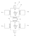
本発明のタンタル窒化物の形成方法は、いわゆるCVD法を実施できる成膜装置であれば特に制約なく実施できる。例えば、図1に示すプラズマCVD成膜装置を使用して本発明方法を実施する場合の一実施の形態について、以下説明する。 The tantalum nitride forming method of the present invention can be carried out without any limitation as long as it is a film forming apparatus capable of performing a so-called CVD method. For example, an embodiment in which the method of the present invention is carried out using the plasma CVD film forming apparatus shown in FIG. 1 will be described below.
図1に示すプラズマCVD装置は、成膜室である真空チャンバ1からなり、この真空チャンバの壁壁には真空排気系2を接続するための開口が設けられ、真空チャンバの上方部には真空チャンバと絶縁した状態で電極3が配置されている。この電極3に接続された高周波電源4が真空チャンバ1の外部に配置されており、電極に高周波電力を印加し、真空チャンバ内にプラズマを発生させることができるように構成されている。真空チャンバ1内には、その下方部にヒータ等の加熱手段5を内蔵する基板載置用ステージ6が、その基板載置面を電極面と互いに平行して対向するように配設されている。
The plasma CVD apparatus shown in FIG. 1 includes a
電極3の内部には、ガス室7が設けられ、電極の基板載置用ステージ6に対向する面にはシャワーノズルとして機能する複数の孔8が開口され、この孔からガスを真空チャンバ内へ導入し、基板表面へ供給できるように構成されており、この電極はシャワープレートとして機能する。
A
ガス室7には、ガス導入系9の一端が接続され、このガス導入系の他端には原料ガスやNH3ガスやH原子含有ガス等がそれぞれ充填された複数のガスボンベ(図示せず)が接続されている。この場合、ガス室7にガス導入系9が複数接続され、それぞれが、別個のガスボンベに接続されていてもよい。図示していないが、マスフローコントローラで各ガス流量を制御できるようになっている。
One end of a gas introduction system 9 is connected to the
原料ガスは、原料ガス充填ガスボンベを用いて導入することもできるが、その他に、上記タンタル含有有機金属化合物を加熱保温された容器内に収容し、バブリングガスとしてのAr等の不活性ガスをマスフローコントローラー等を介して容器内に供給して原料を昇華させ、このバブリングガスと共に原料ガスを真空チャンバ内へ導入するようにしてもよいし、気化器等を介して気化された原料ガスを真空チャンバ内へ導入してもよい。 The source gas can be introduced using a source gas filling gas cylinder. In addition, the tantalum-containing organometallic compound is contained in a heated and heat-insulated container, and an inert gas such as Ar as a bubbling gas is mass-flowed. The raw material gas may be sublimated by supplying it into the container through a controller or the like, and the raw material gas may be introduced into the vacuum chamber together with the bubbling gas, or the raw material gas vaporized through the vaporizer or the like It may be introduced inside.
図1に示すプラズマCVD成膜装置を用い、本発明のタンタル窒化物形成方法を実施するプロセスの一実施の形態は、以下の通りである。 An embodiment of a process for implementing the tantalum nitride forming method of the present invention using the plasma CVD film forming apparatus shown in FIG. 1 is as follows.
まず、真空排気系2により、真空チャンバー1内を所定の圧力(例えば、10−4〜10−5Pa)まで真空排気し、基板載置用ステージ6上に基板Sを載置した後、加熱手段5に通電して基板を所定の温度(例えば、150〜300℃)に加熱する。次いで、ガス導入系9からガス室7へ原料ガスとNH3ガスとを導入し、孔8から基板S表面に向かって供給する。この基板Sとしては、特に制限はないが、例えば、公知の下地密着層が絶縁層上に設けられたものであって、その表面が脱ガス等の前処理をしてあるものであってもよい。
First, the inside of the
真空チャンバ1内の圧力が所定の圧力で安定した後、高周波電源4から、周波数27.12MHz、電力密度0.2W/cm2の高周波交流電圧を出力させる。この高周波電源からの交流電圧が電極3に印加されると、カソードとして機能するように構成されている電極3とアノードとして機能するように構成されている基板ホルダー6上に載置された基板S表面との間に原料ガスとNH3ガス又はNHxラジカル(例えば、NH3ガス)とのプラズマが発生する。このプラズマ中で原料ガス及びNH3ガスのラジカルが生成され、基板S表面上で還元反応が起こり、Ta−N−NH3結合を有する還元化合膜が形成される。所定の膜厚を有する還元化合物膜が形成されたら、高周波電源4の動作を停止し、原料ガスとNH3ガスとの導入を停止する。
After the pressure in the
次いで、真空チャンバー1内へガス導入系9を介してH原子含有ガスを導入して活性化する。すなわち、上記したようにして、チャンバー内にプラズマを発生せしめ、このプラズマ中で発生したラジカルを、上記したようにして形成した還元化合物膜の表面に入射して反応せしめ、この還元化合物膜中のTa−N結合を切断除去し、かつ、残っているNに結合した残りのR(R')基を切断除去し、タンタルリッチのタンタル窒化物膜を形成する。所定の膜厚を有するタンタル窒化物膜が形成されたら、高周波電源4の動作を停止し、H原子含有ガスの導入を停止し、基板Sを真空チャンバー1外へ搬出する。
Next, an H atom-containing gas is introduced into the
上記したようにして形成されたタンタル窒化物膜について、AESによって分析したところ、C5%以下、N33〜35%、Ta/N=1.9〜2.0であり、比抵抗は600μΩ・cm以下であった。 When the tantalum nitride film formed as described above was analyzed by AES, it was C5% or less, N33 to 35%, Ta / N = 1.9 to 2.0, and the specific resistance was 600 μΩ · cm or less. Met.
上記したように、プラズマCVD法では、NH3ガスやH原子含有ガス等の反応ガスがプラズマ中で活性化されるので、比較的低温でも薄膜を形成することができる。また、熱CVD法によっても、公知のプロセス条件で上記と同じタンタルリッチのタンタル窒化物膜を形成することができる。 As described above, in the plasma CVD method, a reactive gas such as NH 3 gas or H atom-containing gas is activated in the plasma, so that a thin film can be formed even at a relatively low temperature. Also, the same tantalum-rich tantalum nitride film can be formed under known process conditions by thermal CVD.
上記したようにして所望の膜厚を有するタンタル窒化物膜が形成された基板に対して、例えば、公知のスパッタ成膜法に従って、Ar等のスパッタリングガスを用い、ターゲットに電圧を印加してプラズマを発生させ、ターゲットをスパッタリングして上記タンタル窒化物膜の表面に金属薄膜、すなわち配線膜側密着層(バリア膜側下地層)を形成させてもよい。 For example, according to a known sputtering film forming method, a sputtering gas such as Ar is applied to a substrate on which a tantalum nitride film having a desired film thickness is formed as described above, and a voltage is applied to the target to generate plasma. And a target is sputtered to form a metal thin film, that is, a wiring film side adhesion layer (barrier film side base layer) on the surface of the tantalum nitride film.
以上の工程を経て基板S上に積層膜が形成され、次いで、上記配線膜側密着層の上に、公知の方法により配線膜(例えば、Cu配線膜)を形成する。 A laminated film is formed on the substrate S through the above steps, and then a wiring film (for example, a Cu wiring film) is formed on the wiring film side adhesion layer by a known method.
ところで、本発明のタンタル窒化物形成方法では、このバリア膜が形成される前に、基板S表面に吸着しているガス等の不純物を除去する公知の脱ガス処理を行うことが必要であり、また、この基板上にバリア膜を形成した後に、最終的に例えばCuからなる配線膜が形成される。そのため、この成膜装置を、真空排気可能な搬送室を介して、少なくとも脱ガス室及び配線膜形成室に接続して、基板が搬送用ロボットによって搬送室から成膜装置と脱ガス室と配線膜形成室との間を搬送できるように構成された複合型配線膜形成装置とすれば、前処理から配線膜形成までの一連の工程をこの装置で実施できる。 By the way, in the tantalum nitride forming method of the present invention, it is necessary to perform a known degassing process for removing impurities such as gas adsorbed on the surface of the substrate S before the barrier film is formed. Further, after forming a barrier film on the substrate, a wiring film made of Cu, for example, is finally formed. Therefore, the film forming apparatus is connected to at least the degassing chamber and the wiring film forming chamber via a transfer chamber that can be evacuated, and the substrate is transferred from the transfer chamber to the film forming apparatus, the degassing chamber, and the wiring by the transfer robot If a composite wiring film forming apparatus configured to be able to transport between the film forming chambers, a series of steps from pretreatment to wiring film formation can be performed with this apparatus.
上記したようにして形成されたタンタル窒化物膜に対して、スパッタリング法等のPVD法によりタンタル粒子を打ち込んで、さらにタンタルリッチのタンタル窒化物膜を形成することもできる。例えば、真空チャンバの上方で、基板ホルダーに対向する位置にターゲットが設置されている公知のスパッタリング装置を用いて実施できる。 A tantalum-rich tantalum nitride film can also be formed by implanting tantalum particles into the tantalum nitride film formed as described above by a PVD method such as sputtering. For example, it can be carried out by using a known sputtering apparatus in which a target is installed at a position facing the substrate holder above the vacuum chamber.
このようなスパッタリング装置の場合、ターゲットには、その表面をスパッタリングし、ターゲット構成物質の粒子を放出させるプラズマを発生させるための電圧印加装置が接続されている。ここで用いるターゲットは、上記原料ガスに含まれる金属の構成元素(Ta)を主成分とするもので構成されており、また、電圧印加装置は、高周波発生装置と、ターゲットに接続された電極とから構成されている。スパッタリングガスは、公知の不活性ガス、例えばアルゴンガス、キセノンガス等であればよい。 In the case of such a sputtering apparatus, a voltage application apparatus is connected to the target for generating plasma for sputtering the surface of the target and releasing particles of the target constituent material. The target used here is composed mainly of a metal constituent element (Ta) contained in the source gas, and the voltage application device includes a high-frequency generator, an electrode connected to the target, It is composed of The sputtering gas may be a known inert gas such as argon gas or xenon gas.
上記のようにして得られたタンタル窒化物膜であるバリア膜の形成された基板Sをスパッタ室内に載置した後に、スパッタ室内へAr等の不活性ガスを導入して放電させ、原料ガスの構成成分であるタンタルを主構成成分とするターゲットをスパッタリングし、基板上に形成された薄膜中にスパッタリング粒子であるタンタル粒子を入射させるようする。このように、スパッタリングによって、ターゲットから基板表面の薄膜中にタンタルを入射させることができるので、バリア膜中のタンタルの含有率をさらに増加せしめることができ、所望の低抵抗のタンタルリッチのタンタル窒化物膜を得ることができる。なお、原料ガスが有機タンタル化合物であるので、上記スパッタリングによって構成元素(タンタル)が基板の表面に入射することにより、分解が促進されてCやN等の不純物がバリア膜からはじき出されて、不純物の少ない低抵抗のバリア膜を得ることができる。 After placing the substrate S on which the barrier film, which is a tantalum nitride film obtained as described above, is placed in the sputtering chamber, an inert gas such as Ar is introduced into the sputtering chamber and discharged, and the source gas A target having tantalum as a main component as a main component is sputtered so that tantalum particles as sputtering particles are incident on a thin film formed on the substrate. In this way, since tantalum can be incident from the target into the thin film on the substrate surface by sputtering, the tantalum content in the barrier film can be further increased, and the desired low resistance tantalum-rich tantalum nitride can be obtained. A material film can be obtained. Since the source gas is an organic tantalum compound, when the constituent element (tantalum) is incident on the surface of the substrate by the sputtering, decomposition is accelerated and impurities such as C and N are expelled from the barrier film. A low-resistance barrier film with a small amount can be obtained.
このスパッタリングは、タンタル粒子をタンタル窒化物膜中に打ち込んで、CやNをスパッタ除去し、この膜の改質を行うために行われるのであって、タンタル膜を積層するのではないので、タンタル膜が形成されない条件、すなわちタンタル粒子によるエッチングができる条件で行うことが必要である。そのため、例えば、DCパワーとRFパワーとを調整して、DCパワーが低く、かつ、RFパワーが高くなるようにする必要がある。例えば、DCパワーを5kW以下に設定し、RFパワーを高く、例えば400〜800Wとすることで、タンタル膜が形成されない条件が達成できる。RFパワーはDCパワーに依存するので、DCパワーとRFパワーを適宜調整することにより、膜の改質程度を調整できる。また、スパッタリング温度は、通常のスパッタリング温度でよく、例えばタンタル窒化物膜の形成温度と同一温度でよい。 This sputtering is performed to implant tantalum particles into a tantalum nitride film, to sputter and remove C and N, and to modify this film, not to stack a tantalum film. It is necessary to carry out under conditions that do not form a film, that is, conditions that allow etching with tantalum particles. Therefore, for example, it is necessary to adjust the DC power and the RF power so that the DC power is low and the RF power is high. For example, by setting the DC power to 5 kW or less and the RF power high, for example, 400 to 800 W, a condition in which a tantalum film is not formed can be achieved. Since the RF power depends on the DC power, the degree of film modification can be adjusted by appropriately adjusting the DC power and the RF power. The sputtering temperature may be a normal sputtering temperature, for example, the same temperature as the tantalum nitride film formation temperature.
上記したようにして所望の膜厚を有するバリア膜が形成された基板Sに対して、例えば、公知のスパッタ成膜法に従って、Ar等のスパッタリングガスを導入し、電圧印加装置からターゲットに電圧を印加してプラズマを発生させ、ターゲットをスパッタリングして上記バリア膜の表面に金属薄膜、すなわち配線膜側密着層(バリア膜側下地層)を形成させてもよい。 A sputtering gas such as Ar is introduced into the substrate S on which the barrier film having a desired film thickness is formed as described above, for example, according to a known sputtering film forming method, and a voltage is applied from the voltage application device to the target. Plasma may be generated by application, and a target may be sputtered to form a metal thin film, that is, a wiring film side adhesion layer (barrier film side base layer) on the surface of the barrier film.
以上の工程を経て基板S上に積層膜が形成され、次いで、上記配線膜側密着層の上に、公知の方法で配線膜を形成する。 A laminated film is formed on the substrate S through the above steps, and then a wiring film is formed on the wiring film side adhesion layer by a known method.
図2は、図1に示す成膜装置を備えた複合型配線膜形成装置の構成図を模式的に示す。 FIG. 2 schematically shows a configuration diagram of a composite wiring film forming apparatus including the film forming apparatus shown in FIG.
この複合型配線膜形成装置100は、前処理部101と成膜処理部103とこれらをつなぐ中継部102とから構成されている。いずれも、処理を行う前には、内部を真空雰囲気にしておく。
The composite wiring
まず、前処理部101では、搬入室101aに配置された処理前基板を前処理部側搬出入ロボット101bによって脱ガス室101cに搬入する。この脱ガス室101cで処理前基板を加熱し、表面の水分等を蒸発させて脱ガス処理を行う。次に、この脱ガス処理された基板を搬出入ロボット101bによって還元処理室101dに搬入する。この還元処理室101d内では、上記基板を加熱して水素ガス等の還元性ガスによって下層配線のメタル酸化物を除去するアニール処理を行う。
First, in the
アニール処理の終了後、搬出入ロボット101bによって還元処理室101dから上記基板を取り出し、中継部102に搬入する。搬入された基板は、中継部102で成膜処理部103の成膜処理部側搬出入ロボット103aに受け渡される。
After the annealing process is completed, the substrate is taken out from the
受け渡された上記基板は、搬出入ロボット103aによって成膜室103bに搬入される。この成膜室103bは、上記成膜装置1に相当する。成膜室103bでバリア膜及び密着層が形成された積層膜は、搬出入ロボット103aによって成膜室103bから搬出され、配線膜室103cに搬入される。ここで、上記バリア膜(バリア膜上に密着層が形成されている場合は、密着層)の上に配線膜が形成される。配線膜が形成された後、この基板を搬出入ロボット103aによって配線膜室103cから搬出室103dに移動し、搬出する。
The transferred substrate is carried into the
以上の通り、上記バリア膜形成の前後の工程、すなわち、脱ガス工程と配線膜形成工程とを一連で行う上記複合型配線膜形成装置100の構成をとれば、作業効率が向上する。
As described above, if the configuration of the composite wiring
なお、上記複合型配線膜形成装置100の構成は、前処理部101に脱ガス室101cと還元処理室101dとを各々1室ずつ設け、成膜処理部103に成膜室103bと配線膜室103cとを各々1室ずつ設けたが、この構成に限定されるものではない。
The composite wiring
従って、例えば、前処理部101及び成膜処理部103の形状を多角形状にし、各々の面に上記脱ガス室101c及び還元処理室101、並びに成膜室103b及び配線膜室103cを複数個設ければ、さらに処理能力は向上する。
Therefore, for example, the
本実施例では、図1に示す成膜装置を用い、原料ガスとしてペンタジメチルアミノタンタル(MO)ガス、NH3ガス及びH原子含有ガスとしてNH3ガスを用いてタンタル窒化物膜を形成した。 In this embodiment, using the film forming apparatus shown in FIG. 1, the penta-dimethylamino tantalum (MO) gas, using NH 3 gas as the NH 3 gas and H atom-containing gas to form a tantalum nitride film as a material gas.
公知の方法に従って、SiO2絶縁膜を有する基板Sの表面の脱ガス前処理工程を実施した後、真空排気系2によって10−5Pa以下に真空排気された真空チャンバ1内に基板Sを搬入した。この基板としては、特に制限はないが、例えば、通常のスパッタ成膜法に従って、Arスパッタリングガスを用い、Taを主構成成分として有するターゲットに電圧を印加してプラズマを発生させ、ターゲットをスパッタリングして表面に基板側密着層を形成させた基板を用いてもよい。
After performing the degassing pretreatment process on the surface of the substrate S having the SiO 2 insulating film according to a known method, the substrate S is carried into the
真空チャンバ1内に基板Sを搬入し、基板載置用ステージ6上に基板Sを載置した後、この基板をヒーター5で250℃に加熱し、ガス導入系9からガス室7へ上記原料ガスを5sccm、上記NH3ガスを100sccm導入し、孔8から基板S表面に向かって供給した。
After the substrate S is carried into the
真空チャンバ1内の圧力が所定の圧力で安定した後、高周波電源4から、周波数27.12MHz、電力密度0.2W/cm2の高周波交流電圧を出力させると、電極3と基板S表面との間に原料ガスとNH3ガスとのプラズマが発生した。このプラズマ中で原料ガス及びNH3ガスのラジカルを生成せしめて、基板S表面上での酸化反応によって、Ta−N−NH3結合を有する還元化合物膜を形成した。所定の膜厚を有する還元化合物膜を形成した後、高周波電源4の動作を停止し、原料ガスと窒素、水素原子含有ガスとの導入を停止した。
After the pressure in the
次いで、真空チャンバー1内へガス導入系9を介して上記H原子含有ガスを導入し、上記したようにして、チャンバー内にプラズマを発生せしめ、このプラズマ中で発生したラジカルを、上記したようにして形成した還元化合物膜の表面に入射して反応せしめた。この反応により、この還元化合物膜中のTa−N結合が切断除去され、かつ、残っているNに結合したR(R')基が切断除去された。その結果、タンタルリッチのタンタル窒化物膜が形成された。所定の膜厚を有するタンタル窒化物膜を形成した後、高周波電源4の動作を停止し、H原子含有ガスの導入を停止し、基板Sを真空チャンバー1外へ搬出した。
Next, the H atom-containing gas is introduced into the
かくして得られたバリア膜の組成は、Ta/N=1.9であり、C含有量は5%以下であり、N含有量は35%であった。 The composition of the barrier film thus obtained was Ta / N = 1.9, the C content was 5% or less, and the N content was 35%.
なお、比較のために、上記原料ガス(MOガス)とNH3ガスとを用いた場合、及び上記原料ガスと反応ガス(Hラジカル)とを用いた場合について、上記方法に準じて成膜した。 For comparison, a film was formed in accordance with the above method when the source gas (MO gas) and NH 3 gas were used, and when the source gas and reaction gas (H radical) were used. .
上記方法で得られたそれぞれの薄膜について、比抵抗ρ(μΩ・cm)を算出した。この比抵抗は、4探針プローブ法でシート抵抗(Rs)を測定し、SEMで膜厚(T)を測定して、式:ρ=Rs・Tに基づいて算出したものである。 The specific resistance ρ (μΩ · cm) was calculated for each thin film obtained by the above method. This specific resistance is calculated based on the formula: ρ = Rs · T by measuring the sheet resistance (Rs) by the four-probe probe method and measuring the film thickness (T) by the SEM.
原料ガス(MOガス)をNH3ガスで還元した後にH原子含有ガス(Hラジカル)を流して成膜した場合には、MOガスとHラジカルとを用いて成膜した場合(2000μΩ・cm)及びMOガスとNH3ガスとを用いて成膜した場合(5000μΩ・cm)よりも低い比抵抗(600μΩ・cm)が得られた。 When the film is formed by flowing H atom-containing gas (H radical) after reducing the source gas (MO gas) with NH 3 gas, the film is formed using MO gas and H radical (2000 μΩ · cm) In addition, a specific resistance (600 μΩ · cm) lower than that obtained when the film was formed using MO gas and NH 3 gas (5000 μΩ · cm) was obtained.
これは、MOガスとHラジカルとの成膜では反応で十分にR(アルキル基)、すなわちCが除去できず、比抵抗が下がらないこと、また、MOガスとNH3ガスとの成膜では、Taリッチの膜が出来にくいことを示すものと考えられる。 This is because in the film formation of MO gas and H radical, R (alkyl group), that is, C cannot be removed sufficiently by reaction, and the specific resistance does not decrease. In the film formation of MO gas and NH 3 gas, This is considered to indicate that it is difficult to form a Ta-rich film.
一方、MOガスとNH3ガスとH原子含有ガスとを用いた成膜では、上記したように、まずNH3により原料ガスのTa−Nの結合が一部切断され、次いでHラジカルの供給により高抵抗の還元化合物におけるTa−N結合が切断されて、残っているR,R'基(アルキル基)が除去されることにより、C、Nの含有割合が減少し、その結果、形成された膜組成がタンタルリッチとなり、膜の比抵抗が下がったことを示しているものと考えられる。 On the other hand, in the film formation using the MO gas, the NH 3 gas, and the H atom-containing gas, as described above, the Ta—N bond of the raw material gas is first partially broken by NH 3 , and then the H radical is supplied. The Ta—N bond in the high-resistance reducing compound is cleaved and the remaining R, R ′ group (alkyl group) is removed, so that the content ratio of C and N is reduced, and as a result, formed. This is considered to indicate that the film composition became tantalum-rich and the specific resistance of the film decreased.
上記したようにして所望の膜厚を有するバリア膜が得られた基板に対し、例えば、公知の方法に従って、Arスパッタリングガスを用い、ターゲットに電圧を印加してプラズマを発生させ、ターゲットをスパッタリングして上記バリア膜の表面に金属薄膜、すなわち下地層としての配線膜側密着層を形成させてもよい。 For the substrate on which a barrier film having a desired film thickness is obtained as described above, for example, according to a known method, an Ar sputtering gas is used to generate a plasma by applying a voltage to the target and sputtering the target. Then, a metal thin film, that is, a wiring film side adhesion layer as an underlayer may be formed on the surface of the barrier film.
以上の工程を経て積層膜が形成された基板S上に、すなわち上記バリア膜側密着層の上に、公知のプロセス条件に従ってCu配線膜を形成した。各膜同士の接着性は優れていることが確認された。 A Cu wiring film was formed on the substrate S on which the laminated film was formed through the above steps, that is, on the barrier film-side adhesion layer according to known process conditions. It was confirmed that the adhesion between the films was excellent.
本実施例では、実施例1で得られたタンタル窒化物膜に対して、公知のスパッタ装置を用いて、スパッタリングによりタンタル粒子を打ち込んで、さらにタンタルリッチのタンタル窒化物膜を形成した。 In this example, a tantalum-rich tantalum nitride film was formed by implanting tantalum particles into the tantalum nitride film obtained in Example 1 by sputtering using a known sputtering apparatus.
スパッタ装置内にArスパッタリングガスを導入し、電圧印加装置からターゲットに電圧を印加して放電させて、プラズマを発生させ、タンタルを主構成成分とするターゲットをスパッタリングし、基板S上に形成された薄膜中にスパッタリング粒子であるタンタル粒子を入射させるようにした。このスパッタリング条件は、DCパワー:5kW、RFパワー:600Wとした。また、スパッタリング温度は、−30〜150℃で行った。 An Ar sputtering gas was introduced into the sputtering apparatus, a voltage was applied to the target from the voltage application apparatus to cause discharge, plasma was generated, and a target containing tantalum as a main component was sputtered to form on the substrate S. Tantalum particles as sputtering particles were allowed to enter the thin film. The sputtering conditions were DC power: 5 kW and RF power: 600 W. Moreover, sputtering temperature was -30-150 degreeC.
上記タンタル粒子を打ち込むスパッタリングにより、バリア膜中のタンタルの含有率をさらに増加せしめることができ、所望の低抵抗のタンタルリッチのタンタル窒化物膜を得ることができた。なお、タンタルが基板Sの表面薄膜中に入射することにより、薄膜の分解が促進されてCやN等の不純物が膜からはじき出されて、不純物の少ない低抵抗のバリア膜を得ることができた。かくして得られた薄膜は、Ta/N=3.5、C及びNの含有量:C=0.1%以下、N=22%、並びに得られた薄膜の比抵抗:90μΩ・cmであった。 By sputtering in which the tantalum particles are implanted, the content of tantalum in the barrier film can be further increased, and a desired low-resistance tantalum-rich tantalum nitride film can be obtained. When tantalum is incident on the surface thin film of the substrate S, decomposition of the thin film is promoted and impurities such as C and N are ejected from the film, so that a low resistance barrier film with few impurities can be obtained. . The thin film thus obtained had Ta / N = 3.5, C and N content: C = 0.1% or less, N = 22%, and the specific resistance of the obtained thin film: 90 μΩ · cm. .
上記のようにして所望の膜厚の改質タンタル窒化物膜が形成された後、例えば、Arスパッタリングガスを導入し、公知のスパッタ成膜プロセス条件に従って電圧印加装置からターゲットに電圧を印加してプラズマを発生させ、ターゲットをスパッタリングして上記バリア膜の表面に金属薄膜、すなわち下地層としての配線膜側密着層を形成させてもよい。 After the modified tantalum nitride film having a desired film thickness is formed as described above, for example, Ar sputtering gas is introduced, and voltage is applied from the voltage application device to the target in accordance with known sputter film formation process conditions. Plasma may be generated and a target may be sputtered to form a metal thin film, that is, a wiring film side adhesion layer as an underlayer on the surface of the barrier film.
以上の工程を経て積層膜が形成された基板S上に、すなわち上記配線膜側密着層の上に、公知のプロセス条件に従ってCu配線膜を形成した。各膜同士の接着性は優れていることが確認された。 A Cu wiring film was formed on the substrate S on which the laminated film was formed through the above steps, that is, on the wiring film-side adhesion layer according to known process conditions. It was confirmed that the adhesion between the films was excellent.
原料ガスとして、ペンタジメチルアミノタンタルの代わりにtert-アミルイミドトリス(ジメチルアミノ)タンタルを用いたこと以外は、実施例1に準じて成膜プロセスを実施したところ、タンタルリッチの低抵抗のタンタル窒化物膜が得られた。得られた膜において、Ta/N=1.8、C含有量5%、N含有量35.7%、並びに得られた薄膜の比抵抗は700μΩ・cmであった。
Except that tert-amylimidotris (dimethylamino) tantalum was used in place of pentadimethylaminotantalum as the source gas, the film forming process was carried out according to Example 1, and tantalum-rich, low-resistance tantalum nitride A material film was obtained. In the obtained film, Ta / N = 1.8,
Hラジカルを生成する反応ガスとして、H2ガスを用いたこと以外は、実施例1に準じて成膜プロセスを実施したところ、実施例1と同様な結果が得られた。 When a film forming process was performed according to Example 1 except that H 2 gas was used as a reaction gas for generating H radicals, the same results as in Example 1 were obtained.
本発明によれば、CVD法に従って、C、N含有量が低く、Ta/N組成比が高く、Cu膜との密着性が確保されるバリア膜として有用な低抵抗のタンタル窒化物膜を形成することができる。そのため、本発明は、半導体デバイス分野の薄膜形成プロセスに適用可能である。 According to the present invention, a low resistance tantalum nitride film which is useful as a barrier film having a low C and N content, a high Ta / N composition ratio and ensuring adhesion with a Cu film is formed according to the CVD method. can do. Therefore, the present invention is applicable to a thin film formation process in the semiconductor device field.
1 真空チャンバ 2 真空排気系
3 電極 4 高周波電源
5 加熱手段 6 基板載置用ステージ
7 ガス室 8 孔
9 ガス導入系 S 基板
DESCRIPTION OF
Claims (7)
Priority Applications (7)
| Application Number | Priority Date | Filing Date | Title |
|---|---|---|---|
| JP2005059085A JP4931173B2 (en) | 2005-03-03 | 2005-03-03 | Method for forming tantalum nitride film |
| TW095106826A TWI397952B (en) | 2005-03-03 | 2006-03-01 | Method for forming tantalum nitride film |
| KR1020097004614A KR100954714B1 (en) | 2005-03-03 | 2006-03-03 | Method for forming tantalum nitride film |
| CN2006800014741A CN101091004B (en) | 2005-03-03 | 2006-03-03 | Method for forming tantalum nitride film |
| KR1020077012311A KR100942685B1 (en) | 2005-03-03 | 2006-03-03 | Method for forming tantalum nitride film |
| PCT/JP2006/304072 WO2006093262A1 (en) | 2005-03-03 | 2006-03-03 | Method for forming tantalum nitride film |
| US11/885,345 US8796142B2 (en) | 2005-03-03 | 2006-03-03 | Method for forming tantalum nitride film |
Applications Claiming Priority (1)
| Application Number | Priority Date | Filing Date | Title |
|---|---|---|---|
| JP2005059085A JP4931173B2 (en) | 2005-03-03 | 2005-03-03 | Method for forming tantalum nitride film |
Publications (3)
| Publication Number | Publication Date |
|---|---|
| JP2006241524A JP2006241524A (en) | 2006-09-14 |
| JP2006241524A5 JP2006241524A5 (en) | 2008-04-24 |
| JP4931173B2 true JP4931173B2 (en) | 2012-05-16 |
Family
ID=36941292
Family Applications (1)
| Application Number | Title | Priority Date | Filing Date |
|---|---|---|---|
| JP2005059085A Active JP4931173B2 (en) | 2005-03-03 | 2005-03-03 | Method for forming tantalum nitride film |
Country Status (6)
| Country | Link |
|---|---|
| US (1) | US8796142B2 (en) |
| JP (1) | JP4931173B2 (en) |
| KR (2) | KR100954714B1 (en) |
| CN (1) | CN101091004B (en) |
| TW (1) | TWI397952B (en) |
| WO (1) | WO2006093262A1 (en) |
Families Citing this family (2)
| Publication number | Priority date | Publication date | Assignee | Title |
|---|---|---|---|---|
| US8048717B2 (en) * | 2007-04-25 | 2011-11-01 | Taiwan Semiconductor Manufacturing Company, Ltd. | Method and system for bonding 3D semiconductor devices |
| CN103839604A (en) * | 2014-02-26 | 2014-06-04 | 京东方科技集团股份有限公司 | Heat conducting film, manufacturing method of heat conducting film, and array substrate |
Family Cites Families (16)
| Publication number | Priority date | Publication date | Assignee | Title |
|---|---|---|---|---|
| KR100200739B1 (en) * | 1996-10-16 | 1999-06-15 | 윤종용 | Method for forming barrier metal wiring |
| US6153519A (en) * | 1997-03-31 | 2000-11-28 | Motorola, Inc. | Method of forming a barrier layer |
| US5893752A (en) * | 1997-12-22 | 1999-04-13 | Motorola, Inc. | Process for forming a semiconductor device |
| US6410432B1 (en) * | 1999-04-27 | 2002-06-25 | Tokyo Electron Limited | CVD of integrated Ta and TaNx films from tantalum halide precursors |
| US6265311B1 (en) * | 1999-04-27 | 2001-07-24 | Tokyo Electron Limited | PECVD of TaN films from tantalum halide precursors |
| US6139922A (en) * | 1999-05-18 | 2000-10-31 | Gelest, Inc. | Tantalum and tantalum-based films formed using fluorine-containing source precursors and methods of making the same |
| US6398929B1 (en) | 1999-10-08 | 2002-06-04 | Applied Materials, Inc. | Plasma reactor and shields generating self-ionized plasma for sputtering |
| KR100403454B1 (en) | 2000-06-20 | 2003-11-01 | 주식회사 하이닉스반도체 | Method of forming a metal wiring in a semiconductor device |
| US7098131B2 (en) * | 2001-07-19 | 2006-08-29 | Samsung Electronics Co., Ltd. | Methods for forming atomic layers and thin films including tantalum nitride and devices including the same |
| US7049226B2 (en) * | 2001-09-26 | 2006-05-23 | Applied Materials, Inc. | Integration of ALD tantalum nitride for copper metallization |
| US7204886B2 (en) * | 2002-11-14 | 2007-04-17 | Applied Materials, Inc. | Apparatus and method for hybrid chemical processing |
| US6916398B2 (en) * | 2001-10-26 | 2005-07-12 | Applied Materials, Inc. | Gas delivery apparatus and method for atomic layer deposition |
| JP2003342732A (en) * | 2002-05-20 | 2003-12-03 | Mitsubishi Materials Corp | Solution raw material for organometallic chemical vapor deposition method containing tantalum complex and tantalum-containing thin film produced by using the same |
| JP2005203569A (en) * | 2004-01-15 | 2005-07-28 | Semiconductor Leading Edge Technologies Inc | Fabrication process of semiconductor device and semiconductor device |
| US20060113603A1 (en) * | 2004-12-01 | 2006-06-01 | Amberwave Systems Corporation | Hybrid semiconductor-on-insulator structures and related methods |
| US8026605B2 (en) * | 2006-12-14 | 2011-09-27 | Lam Research Corporation | Interconnect structure and method of manufacturing a damascene structure |
-
2005
- 2005-03-03 JP JP2005059085A patent/JP4931173B2/en active Active
-
2006
- 2006-03-01 TW TW095106826A patent/TWI397952B/en active
- 2006-03-03 KR KR1020097004614A patent/KR100954714B1/en active IP Right Grant
- 2006-03-03 CN CN2006800014741A patent/CN101091004B/en active Active
- 2006-03-03 US US11/885,345 patent/US8796142B2/en active Active
- 2006-03-03 KR KR1020077012311A patent/KR100942685B1/en active IP Right Grant
- 2006-03-03 WO PCT/JP2006/304072 patent/WO2006093262A1/en active Application Filing
Also Published As
| Publication number | Publication date |
|---|---|
| WO2006093262A1 (en) | 2006-09-08 |
| TWI397952B (en) | 2013-06-01 |
| US20090104775A1 (en) | 2009-04-23 |
| US8796142B2 (en) | 2014-08-05 |
| CN101091004A (en) | 2007-12-19 |
| KR100954714B1 (en) | 2010-04-23 |
| TW200636832A (en) | 2006-10-16 |
| CN101091004B (en) | 2010-08-25 |
| JP2006241524A (en) | 2006-09-14 |
| KR100942685B1 (en) | 2010-02-16 |
| KR20090043554A (en) | 2009-05-06 |
| KR20070085592A (en) | 2007-08-27 |
Similar Documents
| Publication | Publication Date | Title |
|---|---|---|
| JP4931171B2 (en) | Method for forming tantalum nitride film | |
| JP4931170B2 (en) | Method for forming tantalum nitride film | |
| JP4931169B2 (en) | Method for forming tantalum nitride film | |
| JP4931173B2 (en) | Method for forming tantalum nitride film | |
| JP4931174B2 (en) | Method for forming tantalum nitride film | |
| JP4931172B2 (en) | Method for forming tantalum nitride film | |
| US8158197B2 (en) | Method for forming tantalum nitride film |
Legal Events
| Date | Code | Title | Description |
|---|---|---|---|
| RD01 | Notification of change of attorney |
Free format text: JAPANESE INTERMEDIATE CODE: A7421 Effective date: 20080207 |
|
| A521 | Request for written amendment filed |
Free format text: JAPANESE INTERMEDIATE CODE: A523 Effective date: 20080228 |
|
| A621 | Written request for application examination |
Free format text: JAPANESE INTERMEDIATE CODE: A621 Effective date: 20080228 |
|
| A131 | Notification of reasons for refusal |
Free format text: JAPANESE INTERMEDIATE CODE: A131 Effective date: 20110706 |
|
| A521 | Request for written amendment filed |
Free format text: JAPANESE INTERMEDIATE CODE: A523 Effective date: 20110902 |
|
| TRDD | Decision of grant or rejection written | ||
| A01 | Written decision to grant a patent or to grant a registration (utility model) |
Free format text: JAPANESE INTERMEDIATE CODE: A01 Effective date: 20120118 |
|
| A01 | Written decision to grant a patent or to grant a registration (utility model) |
Free format text: JAPANESE INTERMEDIATE CODE: A01 |
|
| A61 | First payment of annual fees (during grant procedure) |
Free format text: JAPANESE INTERMEDIATE CODE: A61 Effective date: 20120213 |
|
| R150 | Certificate of patent or registration of utility model |
Ref document number: 4931173 Country of ref document: JP Free format text: JAPANESE INTERMEDIATE CODE: R150 Free format text: JAPANESE INTERMEDIATE CODE: R150 |
|
| FPAY | Renewal fee payment (event date is renewal date of database) |
Free format text: PAYMENT UNTIL: 20150224 Year of fee payment: 3 |
|
| R250 | Receipt of annual fees |
Free format text: JAPANESE INTERMEDIATE CODE: R250 |
|
| R250 | Receipt of annual fees |
Free format text: JAPANESE INTERMEDIATE CODE: R250 |
|
| R250 | Receipt of annual fees |
Free format text: JAPANESE INTERMEDIATE CODE: R250 |
|
| R250 | Receipt of annual fees |
Free format text: JAPANESE INTERMEDIATE CODE: R250 |
|
| R250 | Receipt of annual fees |
Free format text: JAPANESE INTERMEDIATE CODE: R250 |
|
| R250 | Receipt of annual fees |
Free format text: JAPANESE INTERMEDIATE CODE: R250 |
|
| R250 | Receipt of annual fees |
Free format text: JAPANESE INTERMEDIATE CODE: R250 |
|
| R250 | Receipt of annual fees |
Free format text: JAPANESE INTERMEDIATE CODE: R250 |