JP4889933B2 - Manufacturing method of semiconductor element - Google Patents
Manufacturing method of semiconductor element Download PDFInfo
- Publication number
- JP4889933B2 JP4889933B2 JP2004285912A JP2004285912A JP4889933B2 JP 4889933 B2 JP4889933 B2 JP 4889933B2 JP 2004285912 A JP2004285912 A JP 2004285912A JP 2004285912 A JP2004285912 A JP 2004285912A JP 4889933 B2 JP4889933 B2 JP 4889933B2
- Authority
- JP
- Japan
- Prior art keywords
- film
- organic film
- forming
- organic
- contact hole
- Prior art date
- Legal status (The legal status is an assumption and is not a legal conclusion. Google has not performed a legal analysis and makes no representation as to the accuracy of the status listed.)
- Expired - Fee Related
Links
Images


Description
本発明は、インクジェット法に代表される液滴吐出法を用いた半導体素子の作製方法、特に半導体素子に設けられるコンタクトホールを形成する技術に関するものである。 The present invention relates to a method for manufacturing a semiconductor element using a droplet discharge method typified by an inkjet method, and more particularly to a technique for forming a contact hole provided in the semiconductor element.
半導体素子の作製において、設備の低コスト化、工程の簡略化を目的として、半導体素子に用いられる薄膜や配線のパターン形成に、液滴吐出装置を用いることが検討されている。 In the production of semiconductor elements, the use of a droplet discharge device is being studied for the formation of thin film and wiring patterns used in semiconductor elements for the purpose of reducing equipment costs and simplifying processes.
その際、半導体素子におけるコンタクトホールを形成するにあたっては、レジストを基板全面に塗布形成しプリベークを行った後、マスクを介して紫外線等を照射し、現像によってレジストパターンを形成するというフォトリソグラフィー工程を経た後、該レジストパターンをマスクとしてコンタクトホールとなるべき部分に存在する絶縁膜、半導体膜、導電膜等をエッチング除去することにより、コンタクトホールを形成する方法が用いられていた(特許文献1参照)。
しかしながら、従来の半導体素子の作製工程においてコンタクトホールを開孔する際、コンタクトホールが形成される箇所以外の膜上にレジストを塗布形成しようとすると、ほぼ基板全面にレジストを形成する事になるため、スループットが大幅に低下する。また、スループットを改善したとしても、レジストの塗布量及び下地の表面状態の制御が不十分だと、コンタクトホール部分にもレジストが広がってしまい、コンタクト不良が発生してしまう可能性がある。 However, when a contact hole is formed in a conventional semiconductor device manufacturing process, if a resist is applied and formed on a film other than the portion where the contact hole is formed, the resist is formed on almost the entire surface of the substrate. , Throughput is significantly reduced. Even if the throughput is improved, if the control of the resist coating amount and the surface state of the base is insufficient, the resist spreads in the contact hole portion, and contact failure may occur.
本発明は、このような問題点に鑑みてなされたものであり、簡単な工程で良好なコンタクトホール、及びその周辺に設けられる層間膜、平坦化膜、ゲート絶縁膜等の絶縁膜を形成する方法を提案し、ひいては低コストで、スループットや歩留まりの高い半導体素子の作製方法を提供することを目的とする。 The present invention has been made in view of such problems, and forms a good contact hole and an insulating film such as an interlayer film, a planarizing film, and a gate insulating film provided in the vicinity thereof by a simple process. It is an object of the present invention to propose a method for manufacturing a semiconductor element with low cost and high throughput and yield.
本発明は、半導体素子を形成するにあたって、半導体素子を構成する一の膜上であって、半導体素子のコンタクトホールが形成される部分に、撥液性を有する第1の有機膜(以下「第1の有機膜」という。)を選択的に形成し、該膜が形成されていない領域に第2の有機膜を形成した後に、前記第1の有機膜を除去し、該第1の有機膜が形成されていた部分にコンタクトホールを設けることを特徴としている。 The present invention provides a first organic film (hereinafter referred to as “first organic film”) having a liquid repellency on a portion of a semiconductor element, where a contact hole is formed. The first organic film ”is selectively formed, and the second organic film is formed in a region where the film is not formed. Then, the first organic film is removed, and the first organic film is removed. A feature is that a contact hole is provided in a portion where the film has been formed.
まず、半導体素子を構成する膜上のコンタクトホールを形成すべき箇所に、撥液性(撥水性、撥油性)を有する第1の有機膜を形成する。形成方法としては、インクジェット法に代表される液滴吐出法を用いて吐出形成することができるが、最終的に選択的に形成できるものであれば、これに限定されるものではない。 First, a first organic film having liquid repellency (water repellency, oil repellency) is formed at a position where a contact hole on a film constituting a semiconductor element is to be formed. As a formation method, a droplet discharge method typified by an ink jet method can be used for discharge formation, but the formation method is not limited to this as long as it can be finally selectively formed.
ここで、第1の有機膜が形成される下の膜としては、半導体膜、導電膜、絶縁膜等がある。ここで、半導体膜としては、代表的には、半導体素子におけるソース領域、ドレイン領域、チャネル領域を構成する膜が挙げられるが、これに限定されるものではない。また、導電膜としては、代表的には、半導体素子におけるゲート電極、ソース電極、ドレイン電極、走査線、信号線等の各種配線を構成する膜が挙げられるが、これに限定されるものではない。また、絶縁体膜としては、代表的には、半導体素子におけるゲート絶縁膜、層間絶縁膜、平坦化膜が挙げられるが、これに限定されるものではない。 Here, examples of the lower film on which the first organic film is formed include a semiconductor film, a conductive film, and an insulating film. Here, a typical example of the semiconductor film is a film constituting a source region, a drain region, and a channel region in a semiconductor element, but is not limited thereto. Examples of the conductive film typically include a film that forms various wirings such as a gate electrode, a source electrode, a drain electrode, a scanning line, and a signal line in a semiconductor element, but is not limited thereto. . Examples of the insulator film typically include a gate insulating film, an interlayer insulating film, and a planarization film in a semiconductor element, but are not limited thereto.
次に、第1の有機膜が形成されていない領域に第2の有機膜を形成する。形成方法としては、スピンコート法、液滴吐出法等により、基板上に塗布又は吐出形成すればよい。ここで、第1の有機膜が第2の有機膜に対して撥液性となっているため、第1の有機膜上には第2の有機膜は形成されない。該第2の有機膜は、半導体素子における層間絶縁膜、平坦化膜、ゲート絶縁膜等としての機能を果たす。 Next, a second organic film is formed in a region where the first organic film is not formed. As a formation method, coating or discharge formation may be performed on the substrate by a spin coat method, a droplet discharge method, or the like. Here, since the first organic film is liquid repellent with respect to the second organic film, the second organic film is not formed on the first organic film. The second organic film functions as an interlayer insulating film, a planarizing film, a gate insulating film and the like in the semiconductor element.
次に、第1の有機膜を除去し、該膜が形成されていた部分にコンタクトホールを設ける。除去方法としては、ドライエッチング、ウエットエッチング、大気圧プラズマを用いたエッチングや、水洗処理、あるいはレーザー、電子ビームを用いた処理方法によって選択的に除去すればよい。また、エッチング除去に用いる溶液、溶媒又はガス(エッチャント)や、レーザー等の種類は、第1の有機膜の種類に応じて適宜選択すればよい。 Next, the first organic film is removed, and a contact hole is provided in a portion where the film has been formed. As a removing method, it may be selectively removed by dry etching, wet etching, etching using atmospheric pressure plasma, washing with water, or a processing method using laser or electron beam. Further, the type of solution, solvent or gas (etchant), laser, etc. used for etching removal may be appropriately selected according to the type of the first organic film.
ここで、第1の有機膜が、元来、撥液性を有していない場合には、第2の有機膜を形成する前に、第1の有機膜をプラズマ、レーザー又は電子ビーム等によって処理する。該処理によって、第1の有機膜の表面を撥液性とすることができ、第2の有機膜の付着を防止することができ、良好なコンタクトホールを形成することができる。勿論、第1の有機膜として、元来、撥液性を有している材料を用いる場合には該処理を省略してもよいし、該処理を施すことによって撥液性をより向上させてもよい。 Here, when the first organic film originally has no liquid repellency, the first organic film is formed by plasma, laser, electron beam or the like before forming the second organic film. To process. By this treatment, the surface of the first organic film can be made liquid repellent, adhesion of the second organic film can be prevented, and a good contact hole can be formed. Of course, when a material having liquid repellency is originally used as the first organic film, the treatment may be omitted, and the liquid repellency is further improved by performing the treatment. Also good.
なお、本明細書において、第1の有機膜が、元来、撥液性を有しない又はその程度が低い場合に、所定の処理によって撥液性を有するに至った又は撥液性が向上したものも、「第1の有機膜」と呼ぶこととする。 In the present specification, when the first organic film originally has no liquid repellency or its degree is low, it has liquid repellency or improved liquid repellency by a predetermined treatment. Those are also referred to as “first organic films”.
さらに、第2の有機膜上及び形成されたコンタクトホールの内部に導電膜を形成することにより、上記方法によって形成されたコンタクトホールを介してTFT等の素子と導通を取ることができる。該導電膜は、導電材料を含むペーストを用いた液滴吐出法や、導電材料を含むターゲットを用いたスパッタ法等によって形成すればよい。該導電材料としては、導電膜の機能によって種々の材料を選択することができるが、代表的なものとして、Ag、Au、Cu、Ni、Pt、Pd、Ir、Rh、W、Al、Ta、Mo、Cd、Zn、Fe、Ti、Si、Ge、Zr、Ba等の金属、ハロゲン化銀の微粒子等、又は分散性ナノ粒子、あるいは、透明導電膜として用いられる酸化インジウムスズ(ITO:Indium Tin Oxide)、酸化亜鉛(ZnO:Zinc Oxide)、ガリウムを添加した酸化亜鉛(GZO)、酸化インジウムに2〜20%の酸化亜鉛を混合した酸化インジウム亜鉛(IZO:Indium Zinc Oxide)、有機インジウム、有機スズ、窒化チタン等を用いることができる。また、特に透明導電膜として用いられる材料に対しては、珪素(Si)又は酸化珪素(SiOx)を、上記ペーストやスパッタ用のターゲットに含有させて用いてもよい。例えば、ITOに酸化珪素を含有させた導電材料(通常「ITO−SiOx」と称されるが、以下便宜的に「ITSO」と呼ぶことがある。)を用いることができる。また、これらの材料からなる層を積層させて所望の導電膜を形成してもよい。 Further, by forming a conductive film on the second organic film and inside the formed contact hole, it is possible to conduct with an element such as a TFT through the contact hole formed by the above method. The conductive film may be formed by a droplet discharge method using a paste containing a conductive material, a sputtering method using a target containing a conductive material, or the like. As the conductive material, various materials can be selected depending on the function of the conductive film. Typical examples are Ag, Au, Cu, Ni, Pt, Pd, Ir, Rh, W, Al, Ta, Metals such as Mo, Cd, Zn, Fe, Ti, Si, Ge, Zr, and Ba, fine particles of silver halide, or dispersible nanoparticles, or indium tin oxide (ITO) used as a transparent conductive film Oxide), zinc oxide (ZnO), zinc oxide added with gallium (GZO), indium oxide mixed with 2-20% zinc oxide in indium oxide (IZO: Indium Zinc Oxide), organic indium, organic Tin, titanium nitride, or the like can be used. In particular, for a material used as a transparent conductive film, silicon (Si) or silicon oxide (SiOx) may be contained in the paste or sputtering target. For example, a conductive material in which silicon oxide is contained in ITO (usually referred to as “ITO-SiOx” but may be referred to as “ITSO” for convenience) can be used. Alternatively, a desired conductive film may be formed by stacking layers made of these materials.
さらに、該導電膜の上方に液晶素子や、有機化合物又は無機化合物を含む層からなる発光素子を設けることにより、TFTによって制御可能となる表示装置を得ることができる。このような表示装置は、アクティブマトリクス型表示装置と呼ばれる。 Further, by providing a liquid crystal element or a light-emitting element including a layer containing an organic compound or an inorganic compound above the conductive film, a display device that can be controlled by the TFT can be obtained. Such a display device is called an active matrix display device.
本発明のごとく、第1の有機膜(コンタクトホールとなるべき部分に設けられる膜)として撥液性の材料を用いることにより、層間絶縁膜、平坦化膜、ゲート絶縁膜等として機能する第2の有機膜を、所望の箇所に形成することができる。しかも、レジストマスクを用いた露光・現像プロセス等を経ることなくコンタクトホール、及びその周囲に上記絶縁膜を形成できるため、従来と比較して、工程を大幅に簡略化することができる。また、第1の有機膜上には、第2の有機膜は形成されないため、該第1の有機膜の除去を容易にし、良好なコンタクトホールを簡略なプロセスで形成することができる。 As in the present invention, by using a liquid repellent material as the first organic film (film provided in a portion to be a contact hole), the second functioning as an interlayer insulating film, a planarizing film, a gate insulating film, or the like. This organic film can be formed at a desired location. Moreover, since the insulating film can be formed in and around the contact hole without undergoing an exposure / development process using a resist mask, the process can be greatly simplified as compared with the prior art. In addition, since the second organic film is not formed on the first organic film, the first organic film can be easily removed and a good contact hole can be formed by a simple process.
また、第2の有機膜を形成する前に、第1の有機膜に対してプラズマ、レーザー又は電子ビーム等の処理を施すことによって、第1の有機膜として撥液性を有していない材料を用いた場合にも撥液性を得ることができ、材料の選択性を広げることができる。また、元来、撥液性を有している材料を用いる場合には、該処理を施すことによって撥液性をより向上させることができる。 In addition, a material that does not have liquid repellency as the first organic film by performing treatment such as plasma, laser, or electron beam on the first organic film before forming the second organic film. In the case where is used, liquid repellency can be obtained, and the selectivity of the material can be expanded. In addition, when a material having liquid repellency is originally used, the liquid repellency can be further improved by performing the treatment.
また、第1の有機膜や、導電膜等を形成する際に、液滴吐出法を用いることによって、それらの膜の材料を含む液滴の吐出口であるノズルと基板との相対的な位置を変化させることで任意の場所に液滴を吐出でき、ノズル径、液滴の吐出量及びノズルと吐出物が形成される基板との移動速度の相対的な関係によって、形成するパターンの厚さや太さを調整できるため、それらの膜を所望の箇所に精度良く吐出形成することができる。また、パターニング工程、すなわちレジストマスクを用いた露光・現像プロセスを省略することができるため、工程の大幅な簡略化及びコストの低減を図ることが可能となる。また、液滴吐出法を用いることにより、任意の場所にパターンを形成でき、形成するパターンの厚さや太さを調整できるので、一辺が1〜2mを越えるような大面積の半導体素子基板も、低コストで歩留まり良く製造することができる。 In addition, when the first organic film, the conductive film, or the like is formed, by using a droplet discharge method, the relative position between the nozzle, which is a droplet discharge port including the material of those films, and the substrate It is possible to discharge droplets at any location by changing the thickness of the pattern to be formed, depending on the relative relationship between the nozzle diameter, the droplet discharge amount, and the movement speed of the nozzle and the substrate on which the discharge is formed. Since the thickness can be adjusted, those films can be discharged and formed at a desired location with high accuracy. In addition, since the patterning step, that is, the exposure / development process using a resist mask can be omitted, the process can be greatly simplified and the cost can be reduced. In addition, by using a droplet discharge method, a pattern can be formed at an arbitrary place, and the thickness and thickness of the pattern to be formed can be adjusted. Therefore, a semiconductor element substrate having a large area with one side exceeding 1-2 m It can be manufactured at low cost and high yield.
このように、本発明を用いることによって、半導体素子におけるコンタクトホール、及びその周囲に設けられる絶縁膜を、簡単な工程で精度良く形成することができ、さらには、低コストで、スループットや歩留まりの高い半導体素子の作製方法を提供することができる。 As described above, by using the present invention, the contact hole in the semiconductor element and the insulating film provided around the contact hole can be accurately formed by a simple process, and further, the throughput and the yield can be reduced at low cost. A method for manufacturing a high semiconductor element can be provided.
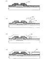
[実施の形態1] 本実施の形態では、図1〜図3を参照して、本発明を逆スタガ型(ボトムゲート型)TFTの作製に適用した場合について説明する。 [Embodiment Mode 1] In this embodiment mode, a case where the present invention is applied to manufacture of an inverted stagger type (bottom gate type) TFT will be described with reference to FIGS.
まず、基板100上に、ゲート電極104、及びゲート電極104に信号を供給する走査線105を形成する。これらは、液滴吐出法を用いて、基板100上に導電材料を含む組成物を選択的に吐出することによって形成するのがよい。この場合、マスクパターンを用いたエッチング工程が不要となるので、作製工程を大幅に簡略化することができる(以上、図1(A))。
First, the
ここで、液滴吐出手段に用いるノズル102の径は、0.1〜50μm(好適には0.6〜26μm)に設定し、ノズル102から吐出される組成物の吐出量は0.00001pl〜50pl(好適には0.0001〜10pl)に設定する。この吐出量は、ノズル102の径の大きさに比例して増加する。また、被処理物とノズル吐出口との距離は、所望の箇所に滴下するために、できる限り近づけておくことが好ましく、好適には0.1〜2mm程度に設定する。
Here, the diameter of the
吐出口から吐出する組成物は、導電体を溶媒に溶解又は分散させたものを用いる。導電体としては、Ag、Au、Cu、Cr、Ni、Pt、Pd、Ir、Rh、W、Al、Ta、Mo、Cd、Zn、Fe、Ti、Si、Ge、Zr、Ba等の金属、ハロゲン化銀の微粒子等、又は分散性ナノ粒子を用いることができる。または、透明導電膜として用いられるITO、ITSO、有機インジウム、有機スズ、酸化亜鉛(ZnO)、窒化チタン(TiN;Titanium Nitride)等を用いることができる。また、これらの材料からなる導電層を積層させてゲート電極104、走査線105を形成してもよい。
A composition in which a conductor is dissolved or dispersed in a solvent is used as the composition discharged from the discharge port. As conductors, metals such as Ag, Au, Cu, Cr, Ni, Pt, Pd, Ir, Rh, W, Al, Ta, Mo, Cd, Zn, Fe, Ti, Si, Ge, Zr, Ba, Silver halide fine particles or the like, or dispersible nanoparticles can be used. Alternatively, ITO, ITSO, organic indium, organic tin, zinc oxide (ZnO), titanium nitride (TiN; Titanium Nitride), or the like used as the transparent conductive film can be used. Alternatively, the
なお、吐出口から吐出する組成物は、比抵抗値を考慮して、金、銀、銅のいずれかの材料を溶媒に溶解又は分散させたものを用いることが好ましい。より好ましくは、低抵抗な銀又は銅を用いるとよい。但し、銅を用いる場合には、不純物対策のため、合わせてバリア膜を設けるとよい。溶媒は、酢酸ブチル、酢酸エチル等のエステル類、イソプロピルアルコール、エチルアルコール等のアルコール類、メチルエチルケトン、アセトン等の有機溶剤等を用いればよい。 In addition, it is preferable to use what dissolved or disperse | distributed the material of either gold | metal | money, silver, and copper in the solvent considering the specific resistance value as the composition discharged from a discharge outlet. More preferably, low resistance silver or copper may be used. However, when copper is used, a barrier film may be provided as a countermeasure against impurities. As the solvent, esters such as butyl acetate and ethyl acetate, alcohols such as isopropyl alcohol and ethyl alcohol, organic solvents such as methyl ethyl ketone and acetone may be used.
ここで、銅を配線として用いる場合のバリア膜としては、窒化シリコン、酸化窒化シリコン、窒化アルミニウム、窒化チタン、窒化タンタル(TaN;Tantalum Nitride)など窒素を含む絶縁性又は導電性の物質を用いると良く、これらを液滴吐出法で形成しても良い。 Here, when a copper film is used as a wiring, an insulating or conductive material containing nitrogen such as silicon nitride, silicon oxynitride, aluminum nitride, titanium nitride, or tantalum nitride (TaN) is used. These may be formed by a droplet discharge method.
なお、液滴吐出法に用いる組成物の粘度は300mPa・s以下が好適であり、これは、乾燥が起こることを防止し、吐出口から組成物を円滑に吐出できるようにするためである。なお、用いる溶媒や用途に合わせて、組成物の粘度、表面張力等は適宜調整するとよい。一例として、ITO、ITSO、有機インジウム、有機スズを溶媒に溶解又は分散させた組成物の粘度は5〜50mPa・s、銀を溶媒に溶解又は分散させた組成物の粘度は5〜20mPa・s、金を溶媒に溶解又は分散させた組成物の粘度は10〜20mPa・sである。 Note that the viscosity of the composition used for the droplet discharge method is preferably 300 mPa · s or less, which is to prevent drying and to smoothly discharge the composition from the discharge port. Note that the viscosity, surface tension, and the like of the composition may be appropriately adjusted according to the solvent to be used and the application. For example, the viscosity of a composition in which ITO, ITSO, organic indium, or organic tin is dissolved or dispersed in a solvent is 5 to 50 mPa · s, and the viscosity of a composition in which silver is dissolved or dispersed in a solvent is 5 to 20 mPa · s. The viscosity of a composition in which gold is dissolved or dispersed in a solvent is 10 to 20 mPa · s.
各ノズルの径や所望のパターン形状などに依存するが、ノズルの目詰まり防止や高精細なパターンの作製のため、導電体の粒子の径はなるべく小さい方が好ましく、好適には粒径0.1μm以下が好ましい。組成物は、電解法、アトマイズ法又は湿式還元法等の公知の方法で形成されるものであり、その粒子サイズは、一般的に約0.5〜10μmである。ただし、ガス中蒸発法で形成すると、分散剤で保護されたナノ分子は約7nmと微細であり、またこのナノ粒子は、被覆剤を用いて各粒子の表面を覆うと、溶剤中に凝集がなく、室温で安定に分散し、液体とほぼ同じ挙動を示す。したがって、被覆剤を用いることが好ましい。 Although depending on the diameter of each nozzle and the desired pattern shape, the diameter of the conductor particles is preferably as small as possible for preventing nozzle clogging and producing a high-definition pattern. 1 μm or less is preferable. The composition is formed by a known method such as an electrolytic method, an atomizing method, or a wet reduction method, and its particle size is generally about 0.5 to 10 μm. However, when formed in a gas evaporation method, the nanomolecules protected by the dispersant are as fine as about 7 nm, and the nanoparticles are aggregated in the solvent when the surface of each particle is covered with a coating agent. And stably disperse at room temperature and shows almost the same behavior as liquid. Therefore, it is preferable to use a coating agent.
なお、ゲート電極104及び走査線105は、予め導電膜を基板全面に成膜しておき、マスクパターンを用いてエッチング形成してもよい。この際、該マスクパターンは、従来通り露光・現像プロセスを行って形成してもよいが、液滴吐出法によって形成する方が工程を簡略化できる点において望ましい。該マスクパターンとしては、アクリル、ベンゾシクロブテン、ポリアミド、ポリイミド、ベンゾイミダゾール又はポリビニルアルコールなどの有機物を含む組成物を、導電膜の上に、液滴吐出ノズル102より選択的に吐出させることで形成することができる。液滴吐出法を用いることで、選択的に組成物を吐出して所望の領域にのみパターンを形成することができる。
Note that the
また、該マスクパターンの材料としては、感光剤を含む組成物でもよく、ポジ型レジストであるノボラック樹脂と感光剤であるナフトキノンジアジド化合物、ネガ型レジストであるベース樹脂、ジフェニルシランジオール及び酸発生剤などを、公知の溶媒に溶解又は分散させたものを用いてもよい。その他、シリコン(Si)と酸素(O)との結合で骨格構造が構成され、置換基に少なくとも水素を含む材料、もしくは置換基にフッ素、アルキル基、または芳香族炭化水素のうち少なくとも一種を有する材料(代表的にはシロキサン系樹脂)を用いてもよい。なお、マスクパターンは、導電膜をエッチング加工する前に焼成して硬化させておくことが望ましい。 The mask pattern material may be a composition containing a photosensitizer, a novolak resin that is a positive resist, a naphthoquinone diazide compound that is a photosensitizer, a base resin that is a negative resist, diphenylsilanediol, and an acid generator. Or the like may be dissolved or dispersed in a known solvent. In addition, a skeletal structure is formed by a bond of silicon (Si) and oxygen (O), and the substituent includes at least one of a material containing at least hydrogen, or a fluorine, an alkyl group, or an aromatic hydrocarbon as a substituent. A material (typically, a siloxane resin) may be used. Note that the mask pattern is preferably baked and cured before the conductive film is etched.
また、エッチング加工によりゲート電極104及び走査線105を形成する場合には、後に形成される半導体膜107との導通を防ぐために、テーパー形状として、ステップカバレッジを良好にしておくのが望ましい。なお、マスクパターンは、エッチング加工した後に除去する。
Further, in the case where the
また、基板100としては、ガラス基板、石英基板、アルミナなど絶縁物質で形成される基板、工程の処理温度に耐え得る耐熱性を有するプラスチック基板等を用いることができる。この場合、酸化シリコン(SiOx)、窒化シリコン(SiNx)、酸化窒化シリコン(SiOxNy)(x>y)、窒化酸化シリコン(SiNxOy)(x>y)など(x、y=1、2・・・)、基板側から不純物などの拡散を防止するための絶縁膜を形成しておくことが望ましい。また、ステンレスなどの金属または半導体基板などの表面に酸化シリコンや窒化シリコンなどの絶縁膜を形成した基板なども用いることができる。
As the
次に、ゲート電極104、走査線105上にゲート絶縁膜106を形成する。ゲート絶縁膜106はプラズマCVD法またはスパッタリング法などの薄膜形成法を用い、窒化シリコン、酸化シリコン、その他の珪素を含む絶縁膜で形成することが好ましい。
Next, a
次に、ゲート絶縁膜106上に、半導体膜107を形成する。半導体膜107としては、アモルファス半導体、結晶性半導体、又はセミアモルファス半導体(SAS)で形成する。いずれも、シリコン、シリコン・ゲルマニウム(SiGe)等を主成分とする半導体膜を用いることができる。また、半導体膜107は、プラズマCVD法などによって形成することができる。なお、半導体膜107の膜厚は、10〜60nmとするのが好ましい。
Next, a
次に、半導体膜107の上に、マスクパターン108を液滴吐出法により形成する。このマスクパターン108はレジストのほか、耐熱性高分子材料を用いて形成することが好ましく、芳香環、複素環を主鎖にもち,脂肪族部分が少なく高極性のヘテロ原子基を含む高分子を用いることが好ましい。そのような高分子物質の代表例としてはポリイミド又はポリベンゾイミダゾールなどが挙げられる。ポリイミドを用いる場合には、ポリイミドを含む組成物を、ノズル127から半導体膜107上に吐出し、200℃で30分焼成して形成することができる(以上、図1(B))。
Next, a
次に、このマスクパターン108を用いて、半導体膜107をエッチングし、島状半導体膜109を形成する。エッチング用ガスとしては、Cl2、BCl3、SiCl4もしくはCCl4などを代表とする塩素系ガス、CF4、SF6、NF3、CHF3などを代表とするフッ素系ガス、あるいはO2を用いることができる。マスクパターン108は、エッチング後に除去する。
Next, the
次に、島状半導体膜109に接してマスクパターン110をゲート電極104と重なる位置に形成する。マスクパターン110は液滴吐出法によりノズル128を用いて島状半導体膜109上に直接描画するようにして形成することができる。液滴組成物は、アクリル、ベンゾシクロブテン、ポリアミド、ポリイミド、ベンゾイミダゾール又はポリビニルアルコールなどの電気絶縁性の膜を形成可能なものを選択する。好適には、ポリイミドを用いると良い。また、マスクパターン110は、島状半導体膜109に不純物元素111をドーピングする際に、マスクとしての機能だけでなくチャネル保護層としての機能も果たすため、その厚さは1μm以上、好ましくは5μm以上の厚さとなるようにするとよい(以上、図1(C))。
Next, a
次に、島状半導体膜109に不純物元素111をドーピングすることにより、島状半導体膜109のうちマスクパターン110に覆われていない領域に、不純物領域を形成する。不純物元素111としては、p型を付与する硼素(B)や、n型を付与する砒素(As)や燐(P)を用いれば良い。ドーピング処理はイオンドープ法、若しくはイオン注入法で行うことができる。このドーピング処理により、島状半導体膜109にはチャネル領域112、不純物が添加されたソース領域113、ドレイン領域114を形成することができる。なお、ドーピング後熱処理による活性化を行っても良い(以上、図2(D))。
Next, an impurity region is formed in a region of the island-shaped
その後、マスクパターン110は剥離してもよいし、剥離せずに後に形成するパッシベーション膜の一部として機能させてもよい。
Thereafter, the
なお、図示しないが、ソース領域113、ドレイン領域114は、島状半導体膜109上にマスクパターン110を残した状態で、さらに不純物が添加された半導体膜を形成し、パターニング工程を経た後にエッチングによって該不純物が添加された半導体膜を分離する方法によって作製してもよい。この場合、マスクパターン110はチャネル保護膜として機能するため、不純物が添加された半導体膜をエッチングする際、チャネル領域となる島状半導体膜109のオーバーエッチング等による損傷を防止することができる。これによって、安定した特性で高移動度化が可能なチャネル保護型(チャネルストッパ型)TFTを得ることができる。なお、ここでいう不純物が添加された半導体膜は、原料ガスであるSiH4、Si2H6、SiH2Cl2、SiHCl3、SiCl4、SiF4ガス等に、硼素、あるいは砒素、燐のような不純物元素を混入させたガスを用い、プラズマCVD法等によって形成すればよい。
Although not illustrated, the
次に、ソース領域113、ドレイン領域114上に、ソース電極115、ドレイン電極116を、また、TFT素子部の周辺にソース信号線117を、導電材料を液滴吐出法によって吐出することにより形成する。導電材料としては、ゲート電極104又は走査線105に用いた材料と同様の材料を、溶媒に溶解又は分散させたものを用いることができる。一例としては、Agを含む組成物(以下「Agペースト」という。)を選択的に吐出し、熱処理により焼成して膜厚600〜800nmの電極を形成する。
Next, the
なお、この焼成をO2雰囲気中で行うと、Agペースト内に含まれているバインダ(熱硬化性樹脂)などの有機物が分解され、有機物をほとんど含まないAg膜を得ることができる。また、膜表面を平滑にすることができる。さらに、Agペーストを減圧下で吐出することにより、ペースト中の溶媒が揮発するため、後の加熱処理を省略、又は加熱処理時間を短縮することができる。 Incidentally, the sintering is performed in an O 2 atmosphere, organic substances such as binders contained in the Ag paste (thermosetting resin) is decomposed, it is possible to obtain a Ag film containing little organic matter. In addition, the film surface can be smoothed. Furthermore, since the solvent in the paste is volatilized by discharging the Ag paste under reduced pressure, the subsequent heat treatment can be omitted or the heat treatment time can be shortened.
なお、ソース電極115、ドレイン電極116は、導電膜を予めスパッタ法等によって成膜しておき、マスクパターンを液滴吐出法によって形成した後に、エッチングにより形成してもよい。このマスクパターンも、上述した材料を用いて形成することができる。
Note that the
次に、ソース電極115、ドレイン電極116上に、パッシベーション膜118を成膜する。パッシベーション膜118は、プラズマCVD法又はスパッタリング法などの薄膜形成法を用い、窒化珪素、酸化珪素、窒化酸化珪素、酸化窒化珪素、酸化窒化アルミニウム、または酸化アルミニウム、ダイアモンドライクカーボン(DLC)、窒素含有炭素(CN)、その他の絶縁性材料を用いて形成することができる。また、マスクパターン110と同様の材料を用いてもよい。さらに、これらの材料を積層させて形成してもよい。なお、パッシベーション膜118は、TFT上方からの不純物の拡散等を防止する機能を有するため、できるだけ形成しておくのが望ましい(以上、図2(E))。
Next, a
次に、パッシベーション膜118上で、かつTFTのソース電極115又はドレイン電極116、及び走査線105、ソース信号線117と導通を取るためのコンタクトホールを形成すべき箇所に、撥液性を有する第1の有機膜119をノズル129を用いて液滴吐出法によって選択的に形成する(図2(F))。
Next, a liquid-repellent first layer is formed on the
第1の有機膜119としては、良好な撥液性を有するRn−Si−X4-n(n=1、2、3)の化学式で表されるシランカップリング剤を用いることができる。好ましくは、フッ素系シランカップリング剤であるフルオロアルキルシラン(FAS;Fluoro Alkyl Silane)を用いる。
As the first
ここで、Rは、アルキル基などの比較的不活性な基、又はビニル基、アミノ基あるいはエポキシ基などの反応性基を含む物である。また、Xはハロゲン、メトキシ基、エトキシ基又はアセトキシ基など基質表面の水酸基あるいは吸着水との縮合により結合可能な加水分解基からなる。FASにおけるRは、(CF3)(CF2)x(CH2)y(x:0以上10以下の整数、y:0以上4以下の整数)で表される構造を持ち、複数個のR又はXがSiに結合している場合には、R又はXはそれぞれすべて同じでも良いし、異なっていてもよい。 Here, R is a substance containing a relatively inactive group such as an alkyl group or a reactive group such as a vinyl group, an amino group or an epoxy group. X consists of a hydroxyl group on the substrate surface such as halogen, methoxy group, ethoxy group or acetoxy group, or a hydrolyzable group capable of binding by condensation with adsorbed water. R in FAS has a structure represented by (CF 3 ) (CF 2 ) x (CH 2 ) y (x: an integer from 0 to 10 and y: an integer from 0 to 4). Alternatively, when X is bonded to Si, R and X may all be the same or different.
なお、第1の有機膜として特にFAS等のフッ素系シランカップリング剤を用いる場合には、それは単分子膜であることから、その膜厚は非常に薄い。本明細書においては、その膜厚を誇張して描いている。したがって、第2の有機膜よりも膜厚が薄くなる場合もある。これは、第1の有機膜としてPVA等の他の材料を用いた場合においても同様である。 Note that when a fluorine-based silane coupling agent such as FAS is used as the first organic film, the film thickness is very thin because it is a monomolecular film. In this specification, the film thickness is exaggerated. Therefore, the film thickness may be thinner than the second organic film. This is the same when other materials such as PVA are used as the first organic film.
第1の有機膜119の形成方法は次の要領で行う。ここでは、シランカップリング剤を用いた場合について説明する。まず、シランカップリング剤を、第1の有機膜を形成する箇所にスピンコート法等によって選択的に塗布する。次に、室温下に放置してシランカップリング剤を乾燥させ、必要に応じて水洗処理を行う。最後に、シランカップリング剤を焼成することにより、CF2鎖、CF3鎖を含むシロキサンネットワーク(SiとOとの結合で骨格構造が構成され、置換基に少なくとも水素を含む、もしくは置換基にフッ素、アルキル基、または芳香族炭化水素のうち少なくとも一種を有する構造)が構築される。なお、乾燥、及び水洗処理は省略してもよい。このCF2、CF3の存在によって、シランカップリング剤による表面処理を行った膜の表面は撥液性を有するようになる。
A method for forming the first
なお、シランカップリング剤は、Rn−Si−X4-n(n=1、2、3)で表される珪素化合物である。ここで、Rは、アルキル基などの比較的不活性な基、又はビニル基、アミノ基あるいはエポキシ基などの反応性基を含む物である。また、Xはハロゲン、メトキシ基、エトキシ基又はアセトキシ基など基質表面の水酸基あるいは吸着水との縮合により結合可能な加水分解基からなる。特に、Rがアルキル機など不活性な基の場合は、改質表面上に、撥水、付着や摩滅の防止、潤滑、つや保持等の性質を付与する。例えば、n=1のものはカップリング剤として、n=2はシロキサンポリマーの原料、n=3はシリル化剤あるいはポリマーのブロック剤(ポリマーの両端を止めるエンドキャッピング剤)として用いられている。 Note that the silane coupling agent is a silicon compound represented by R n -Si-X 4-n (n = 1,2,3). Here, R is a substance containing a relatively inactive group such as an alkyl group or a reactive group such as a vinyl group, an amino group or an epoxy group. X consists of a hydroxyl group on the substrate surface such as halogen, methoxy group, ethoxy group or acetoxy group, or a hydrolyzable group capable of binding by condensation with adsorbed water. In particular, when R is an inert group such as an alkyl machine, properties such as water repellency, prevention of adhesion and abrasion, lubrication, and gloss retention are imparted on the modified surface. For example, n = 1 is used as a coupling agent, n = 2 is used as a raw material for the siloxane polymer, and n = 3 is used as a silylating agent or a polymer blocking agent (end capping agent for stopping both ends of the polymer).
シランカップリング剤の代表的なものとして、フッ素系アルコキシ型シランカップリング剤がある。例えば、CF3(CF2)kCH2CH2Si(OCH3)3、CF3(CF2)kCH2CH2SiCH3(OCH3)2、CF3(CF2)kCH2CH2Si(OCH2CH3)3、(以上、k=3,5,7,9)、あるいは、(CF3)2CF(CF2)mCH2CH2Si(OCH3)3、(CF3)2CF(CF2)mCH2CH2SiCH3(OCH3)2(以上、m=4,6,8)、あるいは、CF3(CF2)j(C6H4)C2H4Si(OCH3)3、CF3(CF2)j(C6H4)C2H4SiCH3(OCH3)2(以上、j=0,3,5,7)が挙げられる。
A typical example of the silane coupling agent is a fluorine-based alkoxy silane coupling agent. For example, CF 3 (CF 2) k
ここで、CF3(CF2)kCH2CH2Si(OCH3)3で、絶縁体であるガラスの表面改質を行った場合のガラス表面の構造を図17に示す。なお、ガラス上に付着した液体(例えば水)に対する接触角は、CF<CF2<CF3の順に増大し、また、フッ化炭素鎖長が長いほど大きくなる傾向にある。 Here, FIG. 17 shows the structure of the glass surface when the surface of the glass as an insulator is modified with CF 3 (CF 2 ) k CH 2 CH 2 Si (OCH 3 ) 3 . In addition, the contact angle with respect to the liquid (for example, water) adhering on the glass increases in the order of CF <CF 2 <CF 3 , and tends to increase as the fluorocarbon chain length increases.
なお、FASとしては、特開2003−80694に示された各種材料を用いることもできる。 In addition, as FAS, various materials shown by Unexamined-Japanese-Patent No. 2003-80694 can also be used.
また、FAS以外で撥液性を有するフッ素系樹脂として、ポリテトラフルオロエチレン(PTFE;四フッ化エチレン樹脂)、パーフルオロアルコキシアルカン(PFA;四フッ化エチレンパーフルオロアルキルビニルエーテル共重合樹脂)、パーフルオロエチレンプロペンコーポリマー(PFEP;四フッ化エチレン−六フッ化プロピレン共重合樹脂)、エチレン−テトラフルオロエチレンコポリマー(ETFE;四フッ化エチレン−エチレン共重合樹脂)、ポリビニリデンフルオライド(PVDF;フッ化ビニリデン樹脂)、ポリクロロトリフルオロエチレン(PCTFE;三フッ化塩化エチレン樹脂)、エチレン−クロロトリフルオロエチレンコポリマー(ECTFE;三フッ化塩化エチレン−エチレン共重合樹脂)、ポリテトラフルオロエチレン−パーフルオロジオキソールコポリマー(TFE/PDD)、ポリビニルフルオライド(PVF;フッ化ビニル樹脂)等を用いることができる。 In addition to FAS, other fluororesins having liquid repellency include polytetrafluoroethylene (PTFE; tetrafluoroethylene resin), perfluoroalkoxyalkane (PFA; tetrafluoroethylene perfluoroalkyl vinyl ether copolymer resin), Fluoroethylene propene copolymer (PFEP; tetrafluoroethylene-hexafluoropropylene copolymer resin), ethylene-tetrafluoroethylene copolymer (ETFE; tetrafluoroethylene-ethylene copolymer resin), polyvinylidene fluoride (PVDF; fluoride) Vinylidene fluoride resin), polychlorotrifluoroethylene (PCTFE; trifluorochloroethylene resin), ethylene-chlorotrifluoroethylene copolymer (ECTFE; trifluoroethylene chloride-ethylene copolymer resin), polytetraflur Roechiren - perfluorodioxole copolymer (TFE / PDD), polyvinyl fluoride (PVF; a vinyl fluoride resin), or the like can be used.
また、第1の有機膜119として、元来、撥液性を有しない有機物を用い、後にCF4プラズマ等による処理を行って、撥液性を得るようにしてもよい。例えば、ポリビニルアルコール(PVA)のような水溶性樹脂を、H2O等の溶媒に混合した材料を用いて、後処理により撥液性を得ることができる。また、PVAと他の水溶性樹脂を組み合わせて使用してもよい。なお、第1の有機膜119が撥液性を有する場合であっても、該プラズマ処理等を行うことによって、撥液性をより向上させることができる。
Alternatively, the first
次に、第2の有機膜120を第1の有機膜119が形成された部分以外の箇所に形成する(図3(G))。第2の有機膜120は、ポリイミド系樹脂、アクリル系樹脂、ポリアミド系樹脂、シロキサン系材料を出発材料として形成されたSi−O結合とSi−CHX結合手を含む絶縁膜等を用い、スピンコート法、液滴吐出法等によって形成することができる。
Next, the second
ここで、第2の有機膜120を形成した際の状態の拡大図を図9(B)に示す。図9(B)において、接触角θは、静止液体の自由表面が固体壁に接する場所で液面と固体面とのなす角と定義される。これは、液体分子間の凝集力と液体と固体壁間の付着力の大小関係によって決まり、液体が固体を濡らす(付着力が大きい)場合には鋭角、濡らさないときは鈍角となる。すなわち、接触角θが大きいほど、付着力は小さくなる、すなわち撥液性は大きくなることが分かる。
Here, an enlarged view of the state when the second
また、第1の有機膜119としてPVAを、第2の有機膜としてポリイミド及びアクリルを用いた場合の接触角の評価を行った結果を図9(A)に示す。評価方法として、まず、基板上にPVAを成膜した後、CF4プラズマ処理を行い、さらにポリイミド溶液(東レ製SL1602)及びアクリル溶液(JSR製SS6699G)を滴下し、それぞれの接触角を評価した。CF4プラズマ処理条件は、パワーを250W又は500Wとし、圧力を0.5Torrとした。
FIG. 9A shows the results of contact angle evaluation when PVA is used as the first
図9(A)のグラフから分かるように、250WのCF4プラズマ処理を30sec施すことにより、ポリイミド(20cp)の場合には接触角が約8°から約45°に増加し、ポリイミド(10cp)の場合には接触角が約8°から約36°に増加し、アクリルの場合には接触角が約9°から37°に増加している。以上、平均して約4〜6倍に増加している。なお、粘度の単位cp=mPa・sである。 As can be seen from the graph of FIG. 9A, the contact angle increases from about 8 ° to about 45 ° in the case of polyimide (20 cp) by applying 250 W of CF 4 plasma treatment for 30 seconds, and polyimide (10 cp) In this case, the contact angle increases from about 8 ° to about 36 °, and in the case of acrylic, the contact angle increases from about 9 ° to 37 °. As described above, the average increases by about 4 to 6 times. The unit of viscosity is cp = mPa · s.
また、CF4プラズマ処理のパワーを500Wと大きくした場合、ポリイミド(20cp)では接触角が約57°、ポリイミド(10cp)では接触角が約54°、アクリルでは接触角が約51°となり、250Wの場合に比べて、接触角が約1.2〜1.5倍に増加した。さらに処理時間を120secと長くした場合、ポリイミドでは接触角が約61〜65°、アクリルでは約51〜54°となり、処理時間を長くすれば、ほとんどパワーによらず一定の接触角を有するようになることがわかる。このように、PVAにCF4プラズマ処理を施すことにより、ポリイミド、アクリル等の第2の有機膜との接触角を増加させる、すなわち両膜間の付着力を弱め、撥液性を高めることができる。 When the power of CF 4 plasma treatment is increased to 500 W, the contact angle is about 57 ° for polyimide (20 cp), the contact angle is about 54 ° for polyimide (10 cp), and the contact angle is about 51 ° for acrylic. The contact angle increased about 1.2 to 1.5 times compared to the case of. Further, when the treatment time is increased to 120 sec, the contact angle is about 61 to 65 ° for polyimide and about 51 to 54 ° for acrylic. If the treatment time is increased, the contact angle is almost constant regardless of the power. I understand that In this way, by applying CF 4 plasma treatment to PVA, the contact angle with the second organic film such as polyimide or acrylic can be increased, that is, the adhesion between the two films can be weakened and the liquid repellency can be improved. it can.
この点に着目し、撥液性を有する第1の有機膜をマスクとして後に層間膜、平坦化膜、ゲート絶縁膜等の絶縁膜として機能する第2の有機膜を良好に形成し、かつ、その後第1の有機膜を除去することにより良好なコンタクトホールを形成することができることを見出した。 Paying attention to this point, a second organic film that functions as an insulating film such as an interlayer film, a planarizing film, and a gate insulating film later is formed satisfactorily using the first organic film having liquid repellency as a mask, and Then, it was found that a good contact hole can be formed by removing the first organic film.
なお、第1の有機膜であるPVAにプラズマ処理を施すことにより、第2の有機膜であるポリイミド又はアクリルとの接触角が35°以上(より好ましくは45°以上)となった場合(図9(A)参照)、第1の有機膜をマスクとして後に絶縁膜として機能する第2の有機膜を形成し、かつ、その後以下の処理によって良好なコンタクトホールを形成することができる。すなわち、接触角が35°以上(より好ましくは45°以上)あれば、第1の有機膜は第2の有機膜に対して撥液性を有していると言える。勿論、パワー250W以上(好ましくは500W)とし、又は処理時間を100sec以上(好ましくは120sec以上)とすることにより、接触角を50°以上(好ましくは、ポリイミドについては60°以上、アクリルについては50°以上)と大きくすることができ、両膜間の付着力は弱まり、より撥液性を高めることができる。これによって、さらに良好なコンタクトホール、及びその周囲に設けられる絶縁膜を形成することができる。 In addition, when PVA which is the first organic film is subjected to plasma treatment, a contact angle with polyimide or acrylic which is the second organic film becomes 35 ° or more (more preferably 45 ° or more) (see FIG. 9 (A)), a second organic film functioning as an insulating film later can be formed using the first organic film as a mask, and a good contact hole can be formed thereafter by the following treatment. That is, if the contact angle is 35 ° or more (more preferably 45 ° or more), it can be said that the first organic film has liquid repellency with respect to the second organic film. Of course, when the power is 250 W or more (preferably 500 W) or the processing time is 100 sec or more (preferably 120 sec or more), the contact angle is 50 ° or more (preferably 60 ° or more for polyimide and 50 for acrylic). The adhesion between the two films is weakened, and the liquid repellency can be further improved. Thereby, a better contact hole and an insulating film provided around the contact hole can be formed.
また、このような相乗効果は、PVAにCF4プラズマ処理を施した場合に限らず、元来、撥液性を有する材料、例えば、フッ素系樹脂であるフルオロアルキルシラン(FAS)等を第1の有機膜として用いることによっても得ることができる(最適な接触角の値は、第1、第2の有機膜の材料によって変化する。)。この場合には、CF4プラズマ処理等の撥液化処理を省略できることは言うまでもないが、さらに撥液性を向上させたい場合には適宜採用してもよい。 Further, such a synergistic effect is not limited to the case where PVA is subjected to CF 4 plasma treatment, but originally a material having liquid repellency, such as fluoroalkylsilane (FAS), which is a fluororesin, is first used. (The optimum contact angle value varies depending on the materials of the first and second organic films). In this case, it goes without saying that a liquid repellency treatment such as a CF 4 plasma treatment can be omitted, but it may be adopted as appropriate in order to further improve the liquid repellency.
第2の有機膜120を形成した後、第1の有機膜119を除去する。また、パッシベーション膜118が形成されている場合には該膜も除去し、該膜走査線105上においてはゲート絶縁膜106も除去する。
After forming the second
第1の有機膜119、パッシベーション膜118及びゲート絶縁膜106の除去方法としては、ウエットエッチング、ドライエッチング、大気圧プラズマ放電を利用したエッチング等を用いてもよいし、水洗処理や、レーザーや電子ビームを用いた処理法を用いてもよい。処理方法は、第1の有機膜119、パッシベーション膜118及びゲート絶縁膜106を構成する材料にあわせて適宜選択することができる。特に、PVA等の水溶性樹脂を用いた場合には、水洗処理によって簡単に除去することができる。また、エッチングガスや溶液(エッチャント)やレーザー等の種類も、材料にあわせて適宜選択することができる。また、第1の有機膜119の除去と、パッシベーション膜118の除去と、ゲート絶縁膜106の除去とを段階的に分けて行ってもよい。
As a method for removing the first
以上の除去処理によって、第1の有機膜119が存在していた箇所、すなわちソース配線115又はドレイン配線116、及び走査線105、ソース信号線117上にコンタクトホール121〜123が形成される。
Through the above-described removal treatment, contact holes 121 to 123 are formed on the portion where the first
なお、第1の有機膜119が完全に除去できるようにエッチング条件を選択、制御するのが望ましいが、コンタクトホールが半導体膜や導電膜等の所望の膜に達していれば、コンタクトホールの側壁に第1の有機膜119が残存しても構わない。第1の有機膜119が残存していても層間膜又は導電膜の一部として十分に機能するからである。この点において、第1の有機膜の材料の選択の幅は広く、また、撥液性を有し、第2の有機膜120を形成するためのマスクとして機能する材料であれば、第1の有機膜に代わる絶縁性材料又は導電材料を用いることも可能である。
Note that it is desirable to select and control the etching conditions so that the first
コンタクトホール121〜123を形成した後、ソース配線115又はドレイン配線116、及び走査線105、ソース信号線117と接続するための導電膜124〜126を形成する。導電材料としては、Ag、Au、Cu、Cr、Ni、Pt、Pd、Ir、Rh、W、Al、Ta、Mo、Cd、Zn、Fe、Ti、Si、Ge、Zr、Ba等の金属、ハロゲン化銀の微粒子等、又は分散性ナノ粒子を用いることができる。または、透明導電膜として用いられるITO、ITSO、有機インジウム、有機スズ、酸化亜鉛、窒化チタン、窒素を50%以下の組成比で含む窒化チタン(以下「Ti(N)」と記す。)等を用いることができる。また、これらの材料からなる導電層を積層させて導電膜124〜126を形成してもよい。
After the contact holes 121 to 123 are formed,
なお、導電膜124〜126は、前記導電材料をスパッタ法等によって形成し、パターニング工程を経た後にエッチング形成してもよいが、液滴吐出法を用いて選択的に形成する方が、工程を大幅に簡略化できる点において望ましい。この場合、導電材料を溶媒に溶解又は分散させたペースト状の材料を、ノズルから吐出形成して該導電膜を形成する。
Note that the
次に、導電膜124の上方に、液晶素子や、有機化合物又は無機化合物を含む層からなる発光素子(代表的にはエレクトロルミネセンス(EL:Electro Luminescence)を利用した発光素子)を設けることにより、上記工程により作製された半導体素子によって制御可能となるアクティブマトリクス型の液晶表示装置や、EL発光装置のような薄型ディスプレイを得ることができる。
Next, a liquid crystal element or a light-emitting element including a layer containing an organic compound or an inorganic compound (typically a light-emitting element using electroluminescence (EL)) is provided above the
なお、上記発光素子は、一対の電極間にキャリア輸送特性の異なる有機化合物又は無機化合物を含む発光層を積層し、一方の電極からは正孔を注入し、他方の電極からは電子を注入できるように形成され、一方の電極から注入された正孔と、他方の電極から注入された電子とが再結合して、それが基底状態に戻るときに光を放出する現象を利用した素子である。発光層への正孔及び電子の注入性は、電極を形成する材料の仕事関数(金属や半導体の表面から、一個の電子を取り出すのに必要な最小のエネルギー)の大小をもって一つの指標とされ、正孔を注入する側の電極には仕事関数が高いことが好ましく、電子を注入する側の電極には仕事関数が低い材料が望まれている。 Note that the light-emitting element can stack a light-emitting layer containing an organic compound or an inorganic compound having different carrier transport properties between a pair of electrodes, inject holes from one electrode, and inject electrons from the other electrode. This is an element that utilizes the phenomenon of emitting light when holes injected from one electrode and electrons injected from the other electrode recombine and return to the ground state. . The injectability of holes and electrons into the light-emitting layer is regarded as an index based on the work function of the material forming the electrode (minimum energy required to extract one electron from the surface of a metal or semiconductor). It is preferable that the electrode on the hole injection side has a high work function, and a material having a low work function is desired for the electrode on the electron injection side.
本発明を用いることにより、レジストマスクを用いた露光・現像プロセス等を経ることなく、コンタクトホール、及び層間膜、平坦化膜、ゲート絶縁膜等の絶縁膜を、簡略化された工程によって精度よく形成することができる。したがって、上記表示装置や、さらにはLSIやCPU等に用いられるあらゆる半導体素子を、低いコストで歩留まり良く製造することができる。 By using the present invention, contact holes and insulating films such as interlayer films, planarization films, and gate insulating films can be accurately obtained by a simplified process without going through an exposure / development process using a resist mask. Can be formed. Therefore, all the semiconductor elements used for the display device, and further for LSI, CPU, etc. can be manufactured at a low cost and with a high yield.
[実施の形態2] 本実施の形態では、図4及び図5を参照して、本発明をトップゲート型TFTの作製に適用した場合について説明する。 [Embodiment Mode 2] In this embodiment mode, a case where the present invention is applied to manufacturing a top gate type TFT will be described with reference to FIGS.
まず、絶縁表面を有する基板100の上に半導体膜401を形成する。基板100は、ガラス、石英、アルミナなど絶縁物質で形成される基板、ステンレスなどの金属または半導体基板などの表面に酸化珪素や窒化珪素などの絶縁膜を形成した基板などを適用することができる。また、液滴吐出法で形成したパターンの焼成温度、或いは半導体膜のソース及びドレイン領域に添加した不純物の活性化処理における熱処理温度などこの工程における最高処理温度に耐えうる耐熱性を有する可撓性、非可撓性のプラスチック基板を用いることもできる。
First, the
半導体膜401は、アモルファス半導体、結晶性半導体、又はセミアモルファス半導体(SAS)によって形成する。いずれも、シリコン、シリコン・ゲルマニウム(SiGe)等を主成分とする半導体膜を用いることができる。また、半導体膜401は、プラズマCVD法などによって形成することができる。なお、半導体膜401の膜厚は、10〜60nmとするのが好ましい。
The
なお、基板100上に下地膜(図示せず)を形成した後に、半導体膜401を形成するのが望ましい。下地膜を設けることにより、基板側から半導体膜401への不純物等の混入を防止することができる。下地膜としては、酸化珪素膜、窒化珪素膜、酸化窒化珪素膜、窒化酸化珪素膜などを用いればよく、単層構造に限らず2層以上積層させた構造を用いてもよい。また、下地膜はプラズマCVD法などによって形成することができる。
Note that the
次に、この半導体膜401をパターニングするために、液滴吐出法を用いてマスクパターン403を形成する。マスクパターン403は、有機樹脂を含む組成物をノズル417より半導体膜401に吐出し、描画することにより直接的に形成する(以上、図4(A))。
Next, in order to pattern the
このマスクパターン403には、アクリル、ベンゾシクロブテン、ポリアミド、ポリイミドなどの有機樹脂を用いればよい。また、シリコン(Si)と酸素(O)との結合で骨格構造が構成され、置換基に少なくとも水素を含む材料、もしくは置換基にフッ素、アルキル基、または芳香族炭化水素のうち少なくとも一種を有する材料(代表的にはシロキサン系樹脂)を用いてもよい。また、感光剤を含む組成物でもよく、ポジ型レジストである、ノボラック樹脂と感光剤であるナフトキノンジアジド化合物、ネガ型レジストであるベース樹脂、ジフェニルシランジオール及び酸発生剤などを、公知の溶媒に溶解又は分散させたものを用いてもよい。
For the
マスクパターン403を用いて、半導体膜401をエッチングして、島状半導体膜404を形成する。エッチング用ガスとしては、Cl2、BCl3、SiCl4もしくはCCl4などを代表とする塩素系ガス、CF4、SF6もしくはNF3などを代表とするフッ素系ガス又はO2を適宜用いることができる。その後、マスクパターン403を剥離除去する。
The
次に、島状半導体膜404上に、ゲート絶縁膜405を形成する。ゲート絶縁膜405はプラズマCVD法またはスパッタリング法を用い、珪素を含む絶縁膜で形成する(以上、図4(B))。
Next, a
次に、ゲート絶縁膜405上に、ゲート電極406を液滴吐出法により形成する(図4(C))。ゲート電極406は導電材料を含む組成物を、ノズル418よりゲート絶縁膜405上に吐出し描画することにより直接的に形成する。導電材料としては、実施の形態1におけるゲート電極の材料と同様のものを用いることができる(図4(C))。
Next, the
次に、ゲート電極406をマスクとして、ゲート絶縁膜405を通して島状半導体膜404に不純物元素407をドーピングすることにより、チャネル領域408、不純物領域であるソース領域409、ドレイン領域410を形成する(図4(D))。なお、ドーピング後熱処理によって活性化を行っても良い。
Next, an
次に、ゲート絶縁膜405上で、かつコンタクトホールが形成されるべき箇所(後にTFTのソース電極、ドレイン電極が形成される箇所)に、撥液性を有する第1の有機膜119を液滴吐出法によってノズル419を用いて選択的に形成する。
Next, the first
第1の有機膜119としては、実施の形態1と同様に、撥液性を有するフッ素系樹脂(好ましくは、フルオロアルキルシラン(FAS))を用いることができる。
As the first
また、第1の有機膜119として撥液性の程度が低い、又は撥液性を有しない有機物を用い、後にCF4プラズマ等による処理を行って、撥液性を得るようにしてもよい。例えば、ポリビニルアルコール(PVA)のような水溶性樹脂を、H2O等の溶媒に混合した材料を用いることができる。また、PVAと他の水溶性樹脂を組み合わせて使用してもよい。
Alternatively, the first
なお、第1の有機膜119がゲート絶縁膜405上ではじく(ゲート絶縁膜405が第1有機膜119に対して撥液性を有する)際には、該膜を形成する前に、ゲート絶縁膜405の表面に対しシランカップリング剤等の撥液性材料を用いた表面処理を行ってもよい。これにより、第1の有機膜119を厚膜とすることができるため、その後形成される第2の有機膜120も厚膜とすることができる。よって、設計上の自由度を向上させることが可能となる。該撥液性材料の形成方法、除去方法は、実施の形態1に準ずる。
Note that when the first
なお、第1の有機膜119が撥液性を有する場合であっても、該プラズマ処理等を行うことによって、撥液性をより向上させることができる。
Note that even when the first
次に、第2の有機膜120を第1の有機膜119が形成されていない領域に形成する。第2の有機膜120は、ポリイミド系樹脂、アクリル系樹脂、ポリアミド系樹脂、シロキサン系材料を出発材料として形成されたSi−O結合とSi−CHX結合手を含む絶縁膜等を用い、スピンコート法、液滴吐出法等によって形成することができる。
Next, the second
第2の有機膜120を形成した後、第1の有機膜119及びゲート絶縁膜405を除去する。第1の有機膜119及びゲート絶縁膜405の除去方法としては、ウエットエッチング、ドライエッチング、大気圧プラズマ放電を利用したエッチング等の種々のエッチング法を用いてもよいし、水洗処理、あるいはレーザーや電子ビームを用いた処理法を用いてもよい。処理方法は、第1の有機膜119及びゲート絶縁膜405を構成する材料にあわせて適宜選択することができる。また、エッチングガスや溶液(エッチャント)やレーザー等の種類も、材料にあわせて適宜選択することができる。また、第1の有機膜119の除去と、ゲート絶縁膜405の除去とを段階的に分けて行ってもよい。
After forming the second
以上の除去処理によって、第1の有機膜119が存在していた箇所、すなわちソース領域409、ドレイン領域410上にコンタクトホール413、414が形成される。
Through the above removal process, contact
なお、第1の有機膜119が完全に除去できるようにエッチング条件を選択、制御するのが望ましいが、コンタクトホールが半導体膜や導電膜等の所望の膜に達していれば、コンタクトホールの側壁に第1の有機膜119が残存しても構わない。第1の有機膜119が残存していても層間膜の一部として十分に機能するからである。この点において、第1の有機膜の材料の選択の幅は広く、また、撥液性を有し、第2の有機膜120を形成するためのマスクとして機能する材料であれば、第1の有機膜に代わる絶縁性材料又は導電材料を用いることも可能である。
Note that it is desirable to select and control the etching conditions so that the first
コンタクトホール413、414を形成した後、ソース電極415及びドレイン電極416を構成する導電材料を形成し、ソース領域409及びドレイン領域410とそれぞれ接続する。電極は、導電材料をスパッタ法等によって形成し、パターニング工程を経た後にエッチング形成してもよいが、液滴吐出法を用いて選択的に形成するのが、工程を大幅に簡略化できる点において望ましい。この場合、導電材料を溶媒に溶解又は分散させたペースト状の材料を、ノズル102から吐出形成して電極を形成する。吐出口から吐出する材料は、導電材料を溶媒に溶解又は分散させたものを用いる。導電材料としてはAg、Au、Cu、Cr、Ni、Pt、Pd、Ir、Rh、W、Al、Ta、Mo、Cd、Zn、Fe、Ti、Si、Ge、Zr、Ba等の金属、ハロゲン化銀の微粒子等、又は分散性ナノ粒子を用いることができる。あるいは、透明導電膜として用いられるITO、ITSO、有機インジウム、有機スズ、酸化亜鉛、窒化チタン、窒素を50%以下の組成比で含む窒化チタン(Ti(N))等を用いることができる。また、これらの材料からなる導電層を積層させて電極を形成してもよい。
After the contact holes 413 and 414 are formed, a conductive material constituting the
なお、吐出口から吐出する組成物は、比抵抗値を考慮して、金、銀、銅のいずれかの材料を溶媒に溶解又は分散させたものを用いることが好ましい。より好ましくは、低抵抗な銀又は銅を用いるとよい。但し、銅を用いる場合には、不純物対策のため、合わせてバリア膜を設けるとよい。溶媒は、酢酸ブチル、酢酸エチル等のエステル類、イソプロピルアルコール、エチルアルコール等のアルコール類、メチルエチルケトン、アセトン等の有機溶剤等を用いればよい。銅を配線として用いる場合のバリア膜としては、窒化シリコン、酸化窒化シリコン、窒化アルミニウム、窒化チタン、窒化タンタルなど窒素を含む絶縁性又は導電性の物質を用いると良く、これらを液滴吐出法で形成しても良い。 In addition, it is preferable to use what dissolved or disperse | distributed the material of either gold | metal | money, silver, and copper in the solvent considering the specific resistance value as the composition discharged from a discharge outlet. More preferably, low resistance silver or copper may be used. However, when copper is used, a barrier film may be provided as a countermeasure against impurities. As the solvent, esters such as butyl acetate and ethyl acetate, alcohols such as isopropyl alcohol and ethyl alcohol, organic solvents such as methyl ethyl ketone and acetone may be used. As a barrier film in the case of using copper as a wiring, an insulating or conductive substance containing nitrogen such as silicon nitride, silicon oxynitride, aluminum nitride, titanium nitride, or tantalum nitride is preferably used. It may be formed.
以上の工程によって、トップゲート型TFTを作製することができる。さらに、該TFTを画素電極と接続し、該画素電極の上方に液晶素子や、有機化合物又は無機化合物を含む層からなる発光素子(代表的にはEL発光素子)を設けることにより、該TFTによって制御可能となるアクティブマトリクス型の液晶表示装置や、EL発光装置のような薄型ディスプレイを得ることができる。 Through the above steps, a top-gate TFT can be manufactured. Further, the TFT is connected to the pixel electrode, and a liquid crystal element or a light emitting element (typically an EL light emitting element) including a layer containing an organic compound or an inorganic compound is provided above the pixel electrode. An active matrix liquid crystal display device that can be controlled and a thin display such as an EL light emitting device can be obtained.
なお、本実施の形態では、ソース電極415及びドレイン電極416が形成される部分のコンタクトホール開孔のために、本発明を利用した形態を示したが、上記工程によって得られたTFTに接続される画素電極が形成される部分のコンタクトホールや、その他ゲート電極406と繋がっている配線が形成される部分のコンタクトホール等の開孔においても、本発明を適用できることは言うまでもない。
Note that in this embodiment mode, an embodiment using the present invention is shown for opening a contact hole in a portion where the
本発明を用いることにより、レジストマスクを用いた露光・現像プロセス等を経ることなく、コンタクトホールを簡略化された工程によって精度よく形成することができる。したがって、上記表示装置や、さらにはLSIやCPU等に用いられるあらゆる半導体素子を低いコストで歩留まり良く製造することができる。 By using the present invention, a contact hole can be accurately formed by a simplified process without going through an exposure / development process using a resist mask. Therefore, all the semiconductor elements used for the display device, and further for LSI, CPU, etc. can be manufactured at a low cost and with a high yield.
なお、図示しないが、基板上にソース電極及びドレイン電極を液滴吐出法によって予め形成し、その後半導体膜、ゲート絶縁膜をプラズマCVD法等によって形成し、ゲート電極を液滴吐出法によって形成し、該ゲート電極をマスクとして、n型又はp型の不純物を半導体膜中に導入するにすることにより、所謂順スタガ型TFTを得ることができる。この順スタガTFTを用いた半導体素子やアクティブマトリクス基板等に作製においても、本発明を利用することができる。 Although not shown, a source electrode and a drain electrode are formed in advance on a substrate by a droplet discharge method, and then a semiconductor film and a gate insulating film are formed by a plasma CVD method or the like, and a gate electrode is formed by a droplet discharge method. A so-called forward stagger type TFT can be obtained by introducing an n-type or p-type impurity into the semiconductor film using the gate electrode as a mask. The present invention can also be used in manufacturing a semiconductor element, an active matrix substrate, or the like using the forward staggered TFT.
本実施例では、図6〜図8を参照して、本発明を用いたアクティブマトリクス型基板の作製方法について説明する。特に、コンタクトホール開孔のための第1の有機膜としてPVAを、第2の有機膜とポリイミド又はアクリルを用いた場合について説明する。 In this embodiment, a method for manufacturing an active matrix substrate using the present invention will be described with reference to FIGS. In particular, the case where PVA is used as the first organic film for opening the contact hole, and the second organic film and polyimide or acrylic are used will be described.
まず、基板600上に、下地絶縁膜601を形成する。ここで、下地絶縁膜601とては、10〜200nmの窒化酸化珪素膜(SiNO)をプラズマCVD法によって形成する。しかし、これに限定されるものではなく、酸化シリコン膜、窒化シリコン膜、酸化窒化シリコン膜あるいはそれらを積層させた構造としても良い。なお、特に下地絶縁膜601を形成しなくてもよい。
First, the
次に、下地絶縁膜601上に10〜80nmの半導体膜を形成する。さらにその表面を、ニッケルを含む溶液で処理した後、500〜750℃の熱結晶化工程によって結晶質シリコン半導体膜を得、さらにレーザー結晶化を行って結晶性の改善を施した。なお、半導体膜としては、シリコン・ゲルマニウム(SiGe)合金など、他の非晶質構造を有する半導体膜を用いても良い。また、成膜方法としては、スパッタ法、LPCVD法などを用いても良いし、結晶化方法としては、レーザー結晶化法、熱結晶化法、他の触媒(Fe,Ru,Rh,Pd,Pd,Os,Ir,Pt,Cu,Au等)を用いた熱結晶化、あるいはそれらを交互に複数回行っても良い。これらの触媒は、溶媒に溶解又は分散させた状態で、スピナーによる塗布、またはスパッタ法等公知の方法によって、該半導体膜上に形成する。例えば、半導体膜の表面に重要換算で10ppmのニッケルを含む酢酸ニッケル塩溶液を塗布することによって行う。
Next, a 10 to 80 nm semiconductor film is formed over the
また、非晶質構造を有する半導体膜の結晶化処理としては、連続発振のレーザーを用いても良く、結晶化に際し大粒径の結晶を得るためには、連続発振が可能な固体レーザーを用い、基本波の第2高調波〜第4高調波を適用するのが好ましい。代表的には、Nd:YVO4レーザー(基本波1064nm)の第2高調波(532nm)や第3高調波(355nm)を適用すればよい。連続発振のレーザーを用いる場合には、出力10Wの連続発振のYVO4レーザーから射出されたレーザー光を非線形光学素子により高調波に変換する。また、共振器の中にYVO4結晶と非線形光学素子を入れて、高調波を射出する方法もある。そして、好ましくは光学系により照射面にて矩形状または楕円形状のレーザー光に成形して、被処理体に照射する。このときのエネルギー密度は0.01〜100MW/cm2程度(好ましくは0.1〜10MW/cm2)が必要である。そして、10〜2000mm/s程度の速度でレーザー光に対して相対的に半導体膜を移動させて照射すればよい。 In addition, a continuous wave laser may be used for the crystallization treatment of the semiconductor film having an amorphous structure, and a solid laser capable of continuous oscillation is used in order to obtain a crystal having a large particle size upon crystallization. It is preferable to apply the second to fourth harmonics of the fundamental wave. Typically, a second harmonic (532 nm) or a third harmonic (355 nm) of an Nd: YVO 4 laser (fundamental wave 1064 nm) may be applied. In the case of using a continuous wave laser, laser light emitted from a continuous wave YVO 4 laser having an output of 10 W is converted into a harmonic by a non-linear optical element. There is also a method of emitting harmonics by putting a YVO 4 crystal and a nonlinear optical element in a resonator. Preferably, the laser beam is shaped into a rectangular or elliptical shape on the irradiation surface by an optical system, and the object to be processed is irradiated. At this time, the energy density of approximately 0.01 to 100 MW / cm 2 (preferably 0.1 to 10 MW / cm 2) is required. Then, irradiation may be performed by moving the semiconductor film relative to the laser light at a speed of about 10 to 2000 mm / s.
上記の方法によって結晶性シリコン半導体膜を得た後、半導体膜上に酸化膜を介して、金属触媒をゲッタリング除去するためのアモルファスシリコン膜を成膜し、500〜750℃の熱処理によってゲッタリング処理を行う。その後、金属触媒を含んだ該アモルファスシリコン膜をエッチング除去する。 After obtaining a crystalline silicon semiconductor film by the above method, an amorphous silicon film for gettering and removing the metal catalyst is formed on the semiconductor film via an oxide film, and gettering is performed by heat treatment at 500 to 750 ° C. Process. Thereafter, the amorphous silicon film containing the metal catalyst is removed by etching.
さらに、TFT素子としての閾値を制御するために、結晶性シリコン半導体膜に対し、ホウ素イオンを1〜3×10¹³atms/cm2程度、あるいはそれ以上の濃度を適宜選択して注入するのが望ましい。 Furthermore, in order to control the threshold value as a TFT element, boron ions are implanted into the crystalline silicon semiconductor film by appropriately selecting a concentration of about 1 to 3 × 10 13 atms / cm 2 or higher. desirable.
その後、結晶性シリコン半導体膜を第1のマスクパターンを用いてエッチングを行い、島状結晶性シリコン半導体膜(以下、単に「島状半導体膜」という。)602〜606を形成する。なお、図示しないが、第1のマスクパターンは、液滴吐出法によって形成するのが工程を簡略化する上で望ましい。この際、第1のマスクパターンは、レジスト又は耐熱性高分子材料を用いて形成することが好ましく、芳香環、複素環を主鎖にもち,脂肪族部分が少なく高極性のヘテロ原子基を含む高分子を用いることが好ましい。そのような高分子物質の代表例としてはポリイミド又はポリベンゾイミダゾールなどが挙げられる。ポリイミドを用いる場合には、ポリイミドを含む組成物を、液滴吐出ノズルから島状半導体膜上に吐出し、200℃で30分焼成して形成することができる After that, the crystalline silicon semiconductor film is etched using the first mask pattern to form island-like crystalline silicon semiconductor films (hereinafter simply referred to as “island-like semiconductor films”) 602 to 606. Although not shown, it is desirable to form the first mask pattern by a droplet discharge method in order to simplify the process. At this time, the first mask pattern is preferably formed using a resist or a heat-resistant polymer material, and has an aromatic ring or a heterocyclic ring as a main chain, and has a small aliphatic portion and a highly polar heteroatom group. It is preferable to use a polymer. Typical examples of such a polymer substance include polyimide and polybenzimidazole. When polyimide is used, it can be formed by discharging a composition containing polyimide onto the island-shaped semiconductor film from a droplet discharge nozzle and baking at 200 ° C. for 30 minutes.
次に、第1のマスクパターンを除去した後、島状半導体膜602〜606上にゲート絶縁膜607を形成する。ゲート絶縁膜607は、プラズマCVD法またはスパッタ法を用い、厚さを1〜200nmに成膜した。好ましくは、10〜50nmと薄くして珪素を含む絶縁膜の単層または積層構造で形成した後に、マイクロ波によるプラズマを用いた表面窒化処理を行う。
Next, after removing the first mask pattern, a
このように膜厚の薄いゲート絶縁膜を、プラズマCVD法を用いて成膜する場合、成膜レートを遅くして薄い膜厚を制御性よく得る必要がある。例えば、RFパワーを100W、10kHz、圧力0.3Torr、N2Oガス流量400sccm、SiH4ガス流量1sccm、とすれば酸化珪素膜の成膜速度を6nm/minとすることができる。また、マイクロ波によるプラズマを用いた窒化処理は、マイクロ波源(2.45GHz)、および反応ガスである窒素ガスを用いて行う。 In the case where the gate insulating film having such a small thickness is formed by using the plasma CVD method, it is necessary to obtain a thin film thickness with good controllability by slowing the film formation rate. For example, if the RF power is 100 W, 10 kHz, the pressure is 0.3 Torr, the N 2 O gas flow rate is 400 sccm, and the SiH 4 gas flow rate is 1 sccm, the deposition rate of the silicon oxide film can be 6 nm / min. Further, nitriding treatment using microwave plasma is performed using a microwave source (2.45 GHz) and nitrogen gas as a reaction gas.
なお、ゲート絶縁膜607表面から離れるにつれて窒素濃度は減少する。これにより酸化珪素膜表面を高濃度に窒化できるだけでなく、酸化珪素膜と活性層の界面の窒素を低減し、デバイス特性の劣化を防ぐ。
Note that the nitrogen concentration decreases as the distance from the surface of the
次に、ゲート絶縁膜607上に膜厚100〜600nmの導電膜608a、608bを形成する。ここでは、スパッタ法を用い、TaN膜とW膜との積層からなる導電膜を形成するが、特にこれに限定されるものではなく、Ag、Au、Cu、Cr、Ni、Pt、Pd、Ir、Rh、Al、Mo、Cd、Zn、Fe、Ti、Si、Ge、Zr、Ba等の金属、又は前記元素を主成分とする合金材料若しくは化合物材料の単層、またはこれらの積層で形成してもよい。また、リン等の不純物元素をドーピングした多結晶シリコン膜に代表される半導体膜を用いてもよい。また、スパッタ法に限らず、液滴吐出法を用いてもよい。
Next,
次に、第2のマスクパターン609a〜609gを形成する。なお、第2のマスクパターン609a〜609gも、第1のマスクパターンと同様に、液滴吐出法によって形成するのが工程を簡略化する上で望ましい(以上、図6(A))。
Next,
次に、第2のマスクパターン609a〜609gをマスクにして、ドライエッチング法またはウエットエッチング法を用いて導電膜608a、608bをエッチングする(第1のエッチング処理)(図6(B))。第1のエッチング処理によって、第1の形状(テーパー状)の画素部TFTのゲート電極610、駆動回路部TFTのゲート電極611〜613、保持容量部の上部電極となる容量配線614、配線615、616を得る。なお、エッチング方法に制限はないが、例えばICP(Inductively Coupled Plasma:誘導結合型プラズマ)エッチング法を用いるとよい。エッチング用ガスとしては、CF4とCl2等を用いる。
Next, using the
次に、第2のマスクパターン609a〜609gをそのまま残した状態で第2のエッチング処理を行い、第2の形状のゲート電極617〜620及び配線621〜623を形成する(図6(C))。
Next, a second etching process is performed in a state where the
続いて、第2の形状のゲート電極617〜620及び配線621〜623をマスクにして、1013〜1014atoms/cm3オーダーのn型不純物元素を島状半導体膜602〜606にドーピング注入する。その後、第2のマスクパターン609a〜609gは、O2アッシング等によって除去する(図6(C))。なお、第2のマスクパターン609a〜609gの除去工程と、ドーピング注入工程とは入れ替えてもよい。
Subsequently, an n-type impurity element of the order of 10 13 to 10 14 atoms / cm 3 is doped into the island-shaped
次に、駆動回路部のpチャネル型TFT652、653及び画素TFT654になる領域の一部を第3のマスクパターン624a、624bで覆い、さらに、1014〜1016atoms/cm2オーダーのn型不純物元素を添加する(図7(D))。これにより、後にソース領域又はドレイン領域になるn型不純物領域(n+)625a、625bと、該n型不純物領域(n+)よりも低濃度の不純物領域626a〜626b(以下「LDD領域」という。)を形成する。さらに、一対のLDD領域の間には、チャネル領域627a、627bがそれぞれ形成される。その後、第3のマスクパターン624a、624bは、O2アッシング等によって除去する。
Next, part of the regions to be the p-channel TFTs 652 and 653 and the
次に、後のnチャネル型TFT651と画素TFT654となる領域に第4のマスクパターン628a、628bを形成し、p型不純物元素を添加して、p型不純物領域629a、629bを形成する(図7(E))。さらに、一対のP型不純物629a、629b領域の間には、チャネル領域630a、630bがそれぞれ形成される。なお、p型不純物領域629a、629bの不純物濃度は、1015〜1017atoms/cm3オーダーとなるようにすればよい。その後、第4のマスクパターン628a、628bは、O2アッシング等によって除去する。
Next,
なお、第3、第4のマスクパターンも、第1、第2のマスクパターンと同様に、液滴吐出法によって形成するのが工程を簡略化する上で望ましい。 The third and fourth mask patterns are preferably formed by the droplet discharge method in the same manner as the first and second mask patterns in order to simplify the process.
次に、TFTを覆うキャップ絶縁膜(図示せず)をプラズマCVD法により形成する。キャップ絶縁膜としては、窒化珪素膜又は酸化窒化珪素膜を用いるのがよいが、これに限定されるものではない。また、形成方法もプラズマCVD法に限定されるものではない。なお、工程を簡略化したい場合には、キャップ絶縁膜は形成しなくてもよい。 Next, a cap insulating film (not shown) covering the TFT is formed by plasma CVD. As the cap insulating film, a silicon nitride film or a silicon oxynitride film is preferably used, but the cap insulating film is not limited to this. Further, the forming method is not limited to the plasma CVD method. Note that the cap insulating film may not be formed in order to simplify the process.
次に、半導体膜に添加された不純物元素の活性化のための加熱処理を行う。この活性化は、N2雰囲気にした炉中において500〜800℃に加熱することによって行う。例えば、RTA(ラピッドサーマルアニール)法を用いることができる。または、レーザー光を照射して活性化を行ってもよい。この場合、基板裏面側又は基板表面側からのみレーザー光を照射してもよいし、基板表面及び裏面の両側から照射してもよい。なお、工程を簡略化したい場合には、該活性化処理を省略してもよい。 Next, heat treatment for activating the impurity element added to the semiconductor film is performed. This activation is performed by heating to 500 to 800 ° C. in a furnace having an N 2 atmosphere. For example, an RTA (rapid thermal annealing) method can be used. Or you may activate by irradiating a laser beam. In this case, the laser beam may be irradiated only from the substrate rear surface side or the substrate front surface side, or from both sides of the substrate front surface and the rear surface. In addition, when it is desired to simplify the process, the activation process may be omitted.
次に、水素を含む窒化珪素膜または窒化酸化珪素膜からなる絶縁膜631をプラズマCVD法により形成する(図7(F))。そして、絶縁膜631から水素を放出させ、半導体膜の水素化を行うための加熱処理を行い、シリコンの不対結合手を終端させる。この加熱処理は、クリーンオーブンを用い、N2雰囲気下において350〜450℃(好ましくは、410℃)で行えばよい。なお、絶縁膜631としては、他の水素及び珪素を含む絶縁膜を用いてもよいし、形成方法もプラズマCVD法以外の方法を用いてもよい。なお、工程を簡略化したい場合には、絶縁膜631の形成及び該水素化処理を省略してもよい。
Next, an insulating
次に、絶縁膜631上で、かつソース領域又はドレイン領域625a〜625c、629a、629b、又は配線623にまで達するコンタクトホールが形成されるべき箇所に、第1の有機膜119を液滴吐出法によって選択的に形成する(図7(F))。ここでは、ポリビニルアルコール(PVA)をH2Oの溶媒に混合した材料を用いて第1の有機膜119を形成する。
Next, the first
次に、第1の有機膜119の表面に対し撥液化処理を行い、該膜の表面を後に形成する第2の有機膜120に対して撥液性を有するようにする。ここでは、CF4プラズマにより撥液化処理を行ったが、この方法に限定されるものではない。また、元来、撥液性を有する有機材料を用いる場合には、該撥液化処理を省略することができる。
Next, liquid repellency treatment is performed on the surface of the first
次に、第2の有機膜120を第1の有機膜119が形成されていない領域に形成する(図8(G))。ここでは、ポリイミドを乳酸エチル及びγブチロラクトンからなる溶媒に溶解し、スピンコート法によって基板全面に塗布するが、この材料、方法に限定されるものではない。例えば、ポリイミド系樹脂の他にも、アクリル系樹脂、ポリアミド系樹脂、シロキサン系材料を出発材料として形成されたSi−O結合とSi−CHX結合手を含む絶縁膜等を用いることができる。また、液滴吐出法等によって形成することもできる。
Next, the second
第2の有機膜120を形成した後、第1の有機膜119、及びその下部に存在するゲート絶縁膜607を除去する。水素化処理のための絶縁膜631、キャップ絶縁膜が形成されている場合にはこれらも除去する。
After the second
ここでは、PVAを含む第1の有機膜119はH2Oを用いて除去した。さらに、その下部のゲート絶縁膜607等は、CF4とO2の混合ガスを用いてドライエッチングによって除去したが、これに限定されるものではない。なお、第1の有機膜119、及びゲート絶縁膜607等をこのように段階的に除去してもよいし、一回で除去してもよい。
Here, the first
このように本実施例で用いたPVAは、H2Oによって簡単に除去できる点において、環境への配慮という観点から優位な材料であるということができる。 Thus, it can be said that PVA used in this example is an advantageous material from the viewpoint of environmental considerations in that it can be easily removed by H 2 O.
上記方法によって第1の有機膜119、及びゲート絶縁膜607等を除去することにより、第1の有機膜119が存在していた箇所、すなわちソース領域又はドレイン領域625a、625b、629a、629b及び配線623上にコンタクトホールが形成される。
By removing the first
コンタクトホールを形成した後、導電材料からなる接続配線634〜641を形成して、それぞれのTFTを電気的に接続する。ここでは、厚さ50〜200nmのTi膜、厚さ250〜400nmのAl膜又はAl−Si合金膜、厚さ50〜200nmのTi膜を積層させて、接続配線634〜641を液滴吐出法によって形成する。ただし、導電材料、方法はこれに限定されるものではなく、実施の形態に示した他の導電材料を用いてもよいし、従来のようにスパッタ法等によって導電材料を形成し、パターニング工程を経た後にエッチング形成してもよい。 After the contact holes are formed, connection wirings 634 to 641 made of a conductive material are formed, and the respective TFTs are electrically connected. Here, a Ti film having a thickness of 50 to 200 nm, an Al film or Al-Si alloy film having a thickness of 250 to 400 nm, and a Ti film having a thickness of 50 to 200 nm are stacked, and the connection wirings 634 to 641 are formed by a droplet discharge method. Formed by. However, the conductive material and method are not limited thereto, and other conductive materials described in the embodiments may be used, and a conductive material is formed by a sputtering method or the like as in the past, and a patterning process is performed. Etching may be performed after the passage.
液滴吐出法を用いる場合、導電材料を溶媒に溶解又は分散させたペースト状の材料を、液滴吐出ノズルから吐出形成して配線を形成する。また、三層構造のうち、TiをTiN、又は窒素を50%以下の組成比で含む窒化チタン(Ti(N))で置き換えてもよいし、TiN又はTi(N)を新たに上下に積層させた構造としてもよい。また、Alは150〜200℃でヒロックが発生してしまうため、Siを含有させておくことが望ましい。 In the case of using the droplet discharge method, a paste material in which a conductive material is dissolved or dispersed in a solvent is discharged from a droplet discharge nozzle to form a wiring. Of the three-layer structure, Ti may be replaced by TiN, or titanium nitride (Ti (N)) containing nitrogen at a composition ratio of 50% or less, or TiN or Ti (N) may be newly stacked above and below. It is good also as the structure made to do. Moreover, since Al will generate hillocks at 150 to 200 ° C., it is desirable to contain Si.
また、画素部658においては、接続配線634〜641形成前に画素電極642を形成する。画素電極642としては、ITO、ITSO、IZO、GZO等の透明導電膜を用いることができ、これらを溶媒に溶解又は分散させたペースト状の材料を用いて液滴吐出法によって形成してもよいし、従来のようにスパッタ法によって形成してもよい。また、これらの材料からなる導電層を積層させた構成としてもよい。なお、画素電極642は、画素TFT654のドレイン領域及び保持容量655の下部電極(不純物が添加された半導体膜)と電気的に接続される。また、画素電極642を接続配線634〜641に形成しても良い。
In the pixel portion 658, the
以上の工程により、nチャネル型TFT651およびpチャネル型TFT652からなるCMOS構造656を含む駆動回路657と、画素TFT654および保持容量655を含む画素部658からなるアクティブマトリクス基板が作製される。
Through the above steps, an active matrix substrate including a driver circuit 657 including a
本実施例を用いたアクティブマトリクス基板の作製方法は、複数のコンタクトホールを開孔するにあたり、第1の有機膜119としてPVAを含む膜を形成し、CF4プラズマ処理を経た後に、第2の有機膜120としてポリイミド又はアクリルを第1の有機膜119の周辺に形成したことにより、簡易な工程で良好なコンタクトホールを精度よく形成することができる。また、コンタクトホールを形成するためのPVA除去はH2Oによって簡単にできるので、環境への配慮という観点からも有益である。
In the method for manufacturing an active matrix substrate using this embodiment, in forming a plurality of contact holes, a film containing PVA is formed as the first
さらに、ゲート電極618〜620、配線621〜623、接続配線634〜641や種々のマスクパターンを液滴吐出法によって形成する場合には、それらの膜の材料を含む液滴の吐出口である液滴吐出ノズルと基板との相対的な位置を変化させることで任意の場所に液滴を吐出でき、ノズル径、液滴の吐出量及びノズルと吐出物が形成される基板との移動速度の相対的な関係によって、形成するパターンの厚さや太さを調整できるため、それらの膜を所望の箇所に精度良く吐出形成することができる。また、レジストマスクを用いた露光・現像プロセス等を省略することができ、工程を大幅に簡略化でき、コストの低減を図ることが可能となる。また、液滴吐出法を用いることにより、任意の場所にパターンを形成でき、形成するパターンの厚さや太さを調整できるので、一辺が1〜2mを越えるような大面積のアクティブマトリクス基板も、低いコストで歩留まり良く製造することができる。
Further, when the
なお、本実施例において、画素部658、駆動回路部657ともに結晶性シリコン半導体膜を用いたが、画素部658においては非晶質半導体膜を用い、高速動作が要求される駆動回路部657においては結晶性半導体膜を用いてもよい。ここで、非晶質半導体膜としては、アモルファスシリコン、シリコン・ゲルマニウム(SiGe)合金をはじめ、他の非晶質構造を有する半導体膜を用いることができる。また、駆動回路部657における結晶性半導体膜としては、セミアモルファスシリコン(SAS)を用いても良い。作製方法としては、基板上に画素部を作製し、画素部と別に作製した駆動回路部とをTAB法などによって接続すればよい。 In this embodiment, a crystalline silicon semiconductor film is used for both the pixel portion 658 and the driver circuit portion 657. However, the pixel portion 658 uses an amorphous semiconductor film, and the driver circuit portion 657 requires high speed operation. May be a crystalline semiconductor film. Here, as the amorphous semiconductor film, semiconductor films having other amorphous structures such as amorphous silicon and silicon-germanium (SiGe) alloy can be used. Further, as the crystalline semiconductor film in the driver circuit portion 657, semi-amorphous silicon (SAS) may be used. As a manufacturing method, a pixel portion is manufactured over a substrate, and a driver circuit portion manufactured separately from the pixel portion may be connected by a TAB method or the like.
ここで、セミアモルファス半導体について説明する。セミアモルファス半導体とは、非晶質と結晶構造(単結晶、多結晶を含む)の中間的な構造を有し、自由エネルギー的に安定な第3の状態を有する半導体であって、短距離秩序を持ち格子歪みを有する結晶質な領域を含んだ半導体をいう。少なくとも膜中の一部の領域には、0.5〜20nmの結晶粒を含んでおり、所謂微結晶半導体(マイクロクリスタル半導体)とも呼ばれる。また、ラマンスペクトルが520cm-1よりも低波数側にシフトしており、X線回折ではSi結晶格子のSi−Siピークに由来するとされる(111)、(220)の回折ピークが観測されるという特徴を有している。また、未結合手(ダングリングボンド)の中和剤として水素またはハロゲンを少なくとも1原子%またはそれ以上含有している。 Here, a semi-amorphous semiconductor will be described. A semi-amorphous semiconductor is a semiconductor having an intermediate structure between amorphous and crystalline structures (including single crystals and polycrystals) and having a third state that is stable in terms of free energy, and has a short-range order. A semiconductor including a crystalline region having lattice distortion. At least part of the region in the film includes crystal grains of 0.5 to 20 nm, and is also called a so-called microcrystalline semiconductor (microcrystal semiconductor). Further, the Raman spectrum is shifted to a lower wave number side than 520 cm −1, and (111) and (220) diffraction peaks that are derived from the Si—Si peak of the Si crystal lattice are observed in X-ray diffraction. It has the characteristics. Further, it contains at least 1 atomic% or more of hydrogen or halogen as a neutralizing agent for dangling bonds.
セミアモルファスシリコンは、SiH4、Si2H6、SiH2Cl2、SiHCl3、SiCl4、SiF4などの珪化物気体をプラズマCVD法によってグロー放電分解して形成する。この珪化物気体をH2、又は、H2とHe、Ar、Kr、Neから選ばれた一種または複数種の希ガス元素で希釈してもよい。希釈率は2〜1000倍の範囲、圧力は概略0.1Pa〜133Paの範囲、電源周波数は1MHz〜120MHz、好ましくは13MHz〜60MHzとするのがよい。また、基板加熱温度は300℃以下、好ましくは100〜250℃とする。膜中の不純物元素のうち、酸素、窒素、炭素などの大気成分の不純物は1×10²⁰atomscm-3以下とすることが望ましく、特に、酸素濃度は5×10¹⁹atoms/cm3以下、好ましくは1×1019atoms/cm3以下とする。なお、セミアモルファスシリコンを用いて作製したTFTの移動度は、μ=1〜10cm2/Vsecである。 Semi-amorphous silicon is formed by glow discharge decomposition of a silicide gas such as SiH 4 , Si 2 H 6 , SiH 2 Cl 2 , SiHCl 3 , SiCl 4 , and SiF 4 by plasma CVD. The silicide gas may be diluted with H 2 , or H 2 and one or more kinds of rare gas elements selected from He, Ar, Kr, and Ne. The dilution rate is in the range of 2 to 1000 times, the pressure is in the range of approximately 0.1 Pa to 133 Pa, and the power supply frequency is 1 MHz to 120 MHz, preferably 13 MHz to 60 MHz. The substrate heating temperature is 300 ° C. or lower, preferably 100 to 250 ° C. Among the impurity elements in the film, impurities of atmospheric components such as oxygen, nitrogen, and carbon are desirably 1 × 10 20 atoms cm −3 or less, and in particular, the oxygen concentration is preferably 5 × 10 19 atoms / cm 3 or less. Is 1 × 10 19 atoms / cm 3 or less. Note that the mobility of a TFT manufactured using semi-amorphous silicon is μ = 1 to 10 cm 2 / Vsec.
本実施例では、特に、コンタクトホール開孔のための第1の有機膜としてフルオロアルキルシラン(FAS)を、第2の有機膜とポリイミド又はアクリルを用いた場合のアクティブマトリクス型基板の作製方法について説明する。 In this embodiment, particularly, a method for manufacturing an active matrix substrate when fluoroalkylsilane (FAS) is used as a first organic film for opening a contact hole and a second organic film and polyimide or acrylic are used. explain.
基板上に、半導体膜、ゲート絶縁膜、ゲート電極等を形成するプロセスは、実施例1又は実施の形態に示した工程と同様である(図6及び図7参照)。また、必要に応じて、キャップ絶縁膜、水素化処理のための絶縁膜を形成してもよい。 A process for forming a semiconductor film, a gate insulating film, a gate electrode, and the like over the substrate is similar to the process described in Example 1 or the embodiment (see FIGS. 6 and 7). Further, a cap insulating film and an insulating film for hydrogenation treatment may be formed as necessary.
図7(F)の状態において、ゲート絶縁膜の上方で、かつソース又はドレイン領域625a、625b、629a、629b、及び配線623にまで達するコンタクトホールが形成されるべき箇所に、Rn−Si−X4-n(n=1、2、3)の化学式で表されるフルオロアルキルシラン(FAS)(第1の有機膜119)を液滴吐出法により選択的に吐出形成する。ここで、Xはメトキシ基、エトキシ基、ハロゲン原子などの加水分解基である。また、Rはフルオロアルキル基であり、(CF3)(CF2)x(CH2)y(x:0以上10以下の整数、y:0以上4以下の整数)で表される構造を持ち、複数個のR又はXがSiに結合している場合には、R又はXはそれぞれすべて同じでも良いし、異なっていてもよい。
In the state of FIG. 7F, R n —Si— is formed at a position where a contact hole reaching the source or
FASとしては、ヘプタデカフルオロ−1,1,2,2テトラヒドロデシルトリエトキシシラン、ヘプタデカフルオロ−1,1,2,2テトラヒドロデシルトリメトキシシラン、ヘプタデカフルオロ−1,1,2,2テトラヒドロデシルトリクロロシラン、トリデカフルオロ−1,1,2,2テトラヒドロオクチルトリエトキシシラン、トリデカフルオロ−1,1,2,2テトラヒドロオクチルトリメトキシシラン、トリデカフルオロ−1,1,2,2テトラヒドロオクチルトリクロロシラン、トリフルオロプロピルトリメトキシシラン等が挙げられる。なお、使用に際しては、一種の化合物を単独で用いてもよいし、二種以上の化合物を組み合わせて使用してもよい。 As FAS, heptadecafluoro-1,1,2,2 tetrahydrodecyltriethoxysilane, heptadecafluoro-1,1,2,2 tetrahydrodecyltrimethoxysilane, heptadecafluoro-1,1,2,2 tetrahydro Decyltrichlorosilane, tridecafluoro-1,1,2,2 tetrahydrooctyltriethoxysilane, tridecafluoro-1,1,2,2 tetrahydrooctyltrimethoxysilane, tridecafluoro-1,1,2,2 tetrahydro Examples include octyltrichlorosilane and trifluoropropyltrimethoxysilane. In use, one kind of compound may be used alone, or two or more kinds of compounds may be used in combination.
次に、第2の有機膜120を第1の有機膜119の周囲に形成する。第1の有機膜119として用いたFASは、単分子であるため膜厚は非常に薄い(0.1nm〜数十nm程度)が、高い撥液性(撥水性、撥油性)を有しているため、CF4プラズマ処理等の疎水化処理を経ることなく、第2の有機膜120を形成することができる。ここでは、ポリイミドを乳酸エチル及びγブチロラクトンからなる溶媒に溶解し、スピンコート法によって基板全面に塗布するが、この材料、方法に限定されるものではない。例えば、ポリイミド系樹脂の他にも、アクリル系樹脂、ポリアミド系樹脂、シロキサン系材料を出発材料として形成されたSi−O結合とSi−CHX結合手を含む絶縁膜等を用いることができる。また、液滴吐出法等によって形成することもできる。
Next, the second
第2の有機膜120を形成した後、第1の有機膜119、及びその下部に存在するゲート絶縁膜607を除去する。水素化処理のための絶縁膜631、キャップ絶縁膜が形成されている場合にはこれらも除去する。
After the second
FASからなる第1の有機膜119は、O2プラズマ、UV処理、UVオゾン処理、O2雰囲気中での熱処理等を用いて簡単に除去することができる。さらに、その下部のゲート絶縁膜607等は、CF4及びO2の混合ガスを用いドライエッチングによって除去したが、これに限定されるものではない。なお、第1の有機膜119、及びゲート絶縁膜607等をこのように段階的に除去してもよいし、一回で除去してもよい。特に、FASは特別な処理(フッ素系シランカップリング剤を用いた表面処理等)をせずとも、O2ガスによってエッチングすることができるので、第1の有機膜119、及びゲート絶縁膜607等を一度に除去することによりコンタクトホールを形成することができ、プロセスを簡略化することができる。
The first
このように本実施例で用いたFASは、元来、高い撥液性を有しているため、撥液性を得るためのCF4プラズマ処理を経る必要がなく、また、CF4及びO2の混合ガス等を用いて他の絶縁膜と同時にエッチング除去できるため、工程を簡略する上で有益な材料である。 As described above, since the FAS used in this example originally has high liquid repellency, it is not necessary to undergo CF 4 plasma treatment for obtaining liquid repellency, and CF 4 and O 2 are not required. This is a useful material for simplifying the process because it can be removed by etching simultaneously with other insulating films using a mixed gas of
上記方法によって第1の有機膜119、及びゲート絶縁膜607等を除去することにより、第1の有機膜119が存在していた箇所、すなわちソース又はドレイン領域625a、625b、629a、629b、及び配線623上にコンタクトホールが形成される。
By removing the first
コンタクトホールを形成した後、導電材料からなる接続配線634〜641を形成して、それぞれのTFTを電気的に接続する。また、画素部には画素電極642を形成する。接続配線634〜641及び画素電極642を構成する導電材料、形成方法は、実施の形態又は実施例1に示したものを採用することができる。
After the contact holes are formed, connection wirings 634 to 641 made of a conductive material are formed, and the respective TFTs are electrically connected. In addition, a
以上の工程により、nチャネル型TFT651およびpチャネル型TFT652からなるCMOS構造656を含む駆動回路657と、画素TFT654および保持容量655を含む画素部658からなるアクティブマトリクス基板が作製される。
Through the above steps, an active matrix substrate including a driver circuit 657 including a
本実施例を用いたアクティブマトリクス基板の作製方法は、複数のコンタクトホールを開孔するにあたり、第1の有機膜119としてFASを形成し、さらに第2の有機膜としてポリイミド又はアクリルを第1の有機膜119の周辺に形成し、第1の有機膜119を除去することにより、簡易な工程で良好なコンタクトホールを精度よく形成することができる。また、コンタクトホールを形成するためのFASはO2を含むガスによって、ゲート絶縁膜等と同時にすることができるので、工程を簡略する上で有益である。
In the manufacturing method of the active matrix substrate using this embodiment, FAS is formed as the first
実施の形態1において、本発明を逆スタガ型TFTの作製に適用した場合について説明したが、本実施例では、図1、図10、図11を参照して、逆スタガ型のうち、チャネルエッチ型(チャネルエッチング型)TFTの作製に本発明を適用した場合について説明する。 In the first embodiment, the case where the present invention is applied to the fabrication of an inverted staggered TFT has been described. In this embodiment, referring to FIGS. 1, 10, and 11, channel etching is included in the inverted staggered type. A case where the present invention is applied to manufacture of a mold (channel etching type) TFT will be described.
まず、基板100上に、ゲート電極104を液滴吐出法によって形成する。ここまでの工程は、実施の形態1と同様に行うことができる(図1(A)参照)。
First, the
次に、ゲート電極104上に、ゲート絶縁膜106を形成する。ここでは、膜厚が100〜400nmの窒化珪素(SiNx)をプラズマCVD法によって形成したが、スパッタリング法などの薄膜形成法を用いてもよい。また、酸化珪素、その他の珪素を含む絶縁膜で形成してもよい。
Next, the
次に、ゲート絶縁膜106上に、半導体膜107を形成する。ここでは、膜厚が10〜300nmのアモルファスシリコン膜を形成したが、他の結晶性半導体、又はセミアモルファス半導体(SAS)で形成してもよい。膜厚は、好ましくは、10〜60nmとするのがよい。次に、半導体膜107上に、n型の半導体膜130を形成する。ここでは、膜厚が40〜60nmのn型(n+)アモルファスシリコン膜を成膜した(以上、図10(A))。
Next, a
ゲート絶縁膜106、半導体膜107及びn型の半導体膜130は、プラズマCVD装置等の同一のチャンバーにおいて、連続的に成膜することができる。なお、TFTの特性安定化と性能向上を図るため、ゲート絶縁膜106の形成温度は300℃以上の高温にし、アモルファスシリコン膜の成膜温度は膜中に混入している水素が脱離しない300℃以下に設定することが望ましい。
The
次に、半導体膜107及びn型の半導体膜130を、第1のマスクパターンを用いて、島状にエッチングし、島上の半導体膜131と半導体膜109を形成する(図10(B))。第1のマスクパターンは、実施の形態1と同様に液滴吐出法を用いて形成することが好ましい。その後、第1のマスクパターンを除去する。
Next, the
次に、島状のn型半導体膜131のうち、ソース領域、ドレイン領域となる部分の上方にソース電極132、ドレイン電極133を液滴吐出法によってノズル138を用いて形成する(図10(C))。導電材料としては、ゲート電極104又は走査線105に用いた材料と同様の材料を、溶媒に溶解又は分散させたものを用いることができる。一例としては、Agを含む組成物を選択的に吐出し、熱処理により焼成して膜厚600〜800nmの電極を形成する。
Next, in the island-shaped n-
なお、ソース電極132、ドレイン電極133は、導電膜を予めスパッタ法等によって成膜しておき、マスクパターンを液滴吐出法によって形成した後に、エッチングにより形成してもよい。
Note that the
次に、ソース電極及びドレイン電極をマスクとして、n型の半導体膜130、及び半導体膜107の上部をエッチング除去する(図10(D))。この際、TFTのチャネル領域となる半導体膜の損傷を抑えるため、適宜エッチング条件を設定する必要がある。
Next, the n-
次に、ソース電極132、ドレイン電極133及び半導体膜107上に、パッシベーション膜118を成膜する(図11(E))。パッシベーション膜118は、プラズマCVD法又はスパッタリング法などの薄膜形成法を用い、窒化珪素、酸化珪素、窒化酸化珪素、酸化窒化珪素、酸化窒化アルミニウム、または酸化アルミニウム、DLC、窒素含有炭素、その他の絶縁性材料を用いて形成することができる。さらに、これらの材料を積層させて形成してもよい。
Next, a
次に、パッシベーション膜118上で、かつソース電極又はドレイン電極に達するコンタクトホールを形成すべき箇所に、第1の有機膜119を液滴吐出法によってノズル139を用いて選択的に形成する。第1の有機膜119としては、実施例1、2で示したPVAやFASを用いるのが望ましいが、これらに限定されるものではない。
Next, a first
次に、第2の有機膜120を第1の有機膜119が形成された部分以外の箇所に形成する。第2の有機膜120は、実施例1、2に示したポリイミド系樹脂、アクリル系樹脂を用いるのが望ましいが、これらに限定されるものではない。
Next, the second
第2の有機膜120を形成した後、第1の有機膜119、及びパッシベーション膜118の一部を除去する。除去方法は、実施例1又は実施例2に示した方法を用いることができる。これにより、第1の有機膜119が存在していた箇所、すなわちソース電極又はドレイン電極上にコンタクトホールが形成される。
After the second
コンタクトホールを形成した後、ソース電極132又はドレイン電極133と接続するための導電膜137を形成する。導電材料としては、透明導電膜であるITO、ITSO、有機インジウム、有機スズ、ZnO、TiN、Ti、Al、Ag、Au、Cu、Cr等を用いることができる。また、これらを主成分とする層を積層させた構造としてもよい。
After the contact hole is formed, a
導電膜137は、前記導電材料をスパッタ法等によって形成し、パターニング工程を経た後にエッチング形成してもよいが、液滴吐出法を用いて選択的に形成する方が、工程を大幅に簡略化できる点において望ましい。この場合、導電材料を溶媒に溶解又は分散させたペースト状の材料を、ノズル102から吐出形成して該導電膜を形成する。なお、導電膜137は、前記導電材料を積層させて形成してもよい。
The
次に、導電膜137の上方に、液晶素子や、有機化合物又は無機化合物を含む層からなる発光素子(代表的にはEL発光素子)を設けることにより、上記工程により作製された半導体素子によって制御可能となるアクティブマトリクス型の液晶表示装置や、EL発光装置のような薄型ディスプレイを得ることができる。
Next, a liquid crystal element or a light-emitting element (typically, an EL light-emitting element) including a layer containing an organic compound or an inorganic compound is provided above the
本実施例で説明したチャネルエッチ型TFTは、作製工程が単純で、構造も簡単であるという利点を有しているが、さらに本発明を適用することにより、レジストマスクを用いた露光・現像プロセス等を経ることなく、コンタクトホール、及び層間膜、平坦化膜、ゲート絶縁膜等の絶縁膜を、簡略化された工程によって精度よく形成することができる。したがって、上記表示装置等に用いられる半導体素子を、低いコストで歩留まり良く製造することができる。 The channel etch type TFT described in this embodiment has an advantage that the manufacturing process is simple and the structure is simple. However, by applying the present invention, an exposure / development process using a resist mask is possible. The insulating film such as the contact hole and the interlayer film, the planarizing film, and the gate insulating film can be accurately formed by a simplified process. Therefore, a semiconductor element used for the display device or the like can be manufactured with low yield and high yield.
本実施例では、実施例1〜3を適応して作製されたTFT基板からアクティブマトリクス駆動の液晶表示装置の構成及び作製工程を説明する。
In this embodiment, a configuration and manufacturing process of an active matrix driving liquid crystal display device from a TFT substrate manufactured by applying
図12は、TFT基板と対向基板180とをシール材で貼り合わせた状態を示している。
FIG. 12 shows a state where the TFT substrate and the
以下、この作製方法を示す。TFT基板上は柱状のスペーサ183を形成する。柱状のスペーサ183は画素電極上に形成されるコンタクト部のくぼみに合わせて形成するとよい。柱状スペーサ183は用いる液晶材料にも依存するが、3〜10μmの高さで形成する。コンタクト部では、コンタクトホールに対応した凹部が形成される場合には、この部分に合わせてスペーサを形成することにより液晶の配向の乱れを防ぐことができる。次に、配向膜182を形成し、ラビング処理を行う。対向基板180には透明導電膜184、配向膜182を形成する。その後、TFT基板および対向基板180をシール材により貼り合わせて液晶を注入し、液晶層185を形成する。以上のようにして、アクティブマトリクス駆動の液晶表示装置を完成させることができる。なお、液晶層185は、液晶を滴下することによって形成してもよい。特に1〜2mを超える大面積のアクティブマトリクス基板を用いて液晶表示装置を作製する場合には、有効な手段である。
Hereinafter, this production method will be described. A
本実施例では、図13を参照して、実施例1〜3により得られるTFT基板(アクティブマトリクス基板)を用いたアクティブマトリクス駆動の発光装置の構成及び作製工程を説明する。
In this embodiment, a configuration and manufacturing process of an active matrix driving light emitting device using a TFT substrate (active matrix substrate) obtained in
基板1601はガラス基板を用いる。このガラス基板1601上には駆動回路部1650にnチャネル型TFT1652とpチャネル型TFT1653が形成され、画素部1651にスイッチング用TFT1654、電流制御用TFT1655が形成されている。これらのTFTは、半導体膜1603〜1606、ゲート絶縁膜1607、ゲート電極1608〜1611などを用いて形成されている。
A glass substrate is used as the
基板1601上に形成する下地絶縁膜1602は酸化窒化シリコン、窒化シリコン膜などを50〜200nmの厚さに形成して設ける。層間絶縁膜は窒化シリコン、酸化窒化シリコンなどで形成される無機絶縁膜1618と、アクリルまたはポリイミドなどで形成される有機絶縁膜1619とから成っている。
The
駆動回路部1650の回路構成は、ゲート信号側駆動回路とデータ信号側駆動回路とで異なるがここでは省略する。nチャネル型TFT1652及びpチャネル型TFT1653には配線1612、1613が接続され、これらのTFTを用いて、シフトレジスタやラッチ回路、バッファ回路などが形成される。
The circuit configuration of the drive circuit unit 1650 differs between the gate signal side drive circuit and the data signal side drive circuit, but is omitted here.
画素部1651では、データ配線1614がスイッチング用TFT1654のソース側に接続し、ドレイン側の配線1615は電流制御用TFT1655のゲート電極1611と接続している。また、電流制御用TFT1655のソース側は電源供給配線1617と接続し、ドレイン側の配線1616がEL素子の陽極(正孔注入電極とも呼ばれる。)1622と接続するように配線されている。
In the pixel portion 1651, the
配線1612〜1617が設けられるコンタクトホールを形成する際に、コンタクトホールが形成される部分に液滴吐出法によって撥液性を有する第1の有機膜を成膜し、その周辺に第2の有機膜を成膜することにより、コンタクトホール及び有機絶縁膜1619を形成することができる。
When forming contact holes in which the
陽極1622、陰極1624及びその間にエレクトロルミネセンス(Electro Luminescence)が得られる有機化合物又は無機化合物を含む層(以下「EL層」と総称する。)1623を有するEL素子1656は画素部1651に形成される。尚、EL層1623におけるルミネセンスには一重項励起状態から基底状態に戻る際の発光(蛍光)と三重項励起状態から基底状態に戻る際の発光(リン光)とがあり、その両者を含むものとする。
An
EL素子1656は、配線を覆うようにアクリルやポリイミドなどの有機樹脂、好適には感光性の有機樹脂を用いて絶縁物1620、1621(隔壁、土手、バンク等と呼ばれる。)を形成した後に設ける。本実施例では、EL素子1656は、ITOで形成される陽極1622、EL層1623、MgAgやLiFなどのアルカリ金属またはアルカリ土類金属などの材料を用いて形成される陰極1624(電子注入電極とも呼ばれる。)とから成っている。絶縁物1620、1621は、陽極1622の端部を覆うように形成され、この部分で陰極1624と陽極1622とがショートすることを防ぐために設ける。なお、絶縁物1620、1621を形成する際に、EL発光素子が形成される部分に液滴吐出法によって撥液性を有する第1の有機膜を成膜し、その周辺に第2の有機膜を成膜することにより、EL発光素子が形成される部分及び絶縁物1620、1621を形成してもよい。
The
ここで、陽極1622は、ITOに限らず、ITSO、ZnO、IZO、GZO等の透明導電膜を用いることもできる。また、陽極1622としてITSOを用いる場合には、濃度の異なる酸化珪素を含むITSOを積層させることによって形成してもよい。好ましくは、下部ITSO層(ソース又はドレイン配線側)の酸化珪素濃度を低濃度に、上部ITSO層(発光層側)の酸化珪素濃度を高濃度にするのがよい。これにより、TFTとの接続間の低抵抗を維持しつつ、EL層1623への正孔注入効率を高めることができる。勿論、他の材料とITSOの積層構造(例えば、下部ITO層と上部ITSO層の積層構造)としてもよいし、他の材料同士を積層させてもよい。
Here, the
また、EL層1623は、蒸着法又は塗布法を用いて形成する。なお、信頼性を向上させるため、EL層1623の形成前に、水銀ランプを光源として用い、紫外線(UV)照射処理を行い、さらに真空加熱を行って脱気を行うことが好ましい。例えば、有機化合物材料の蒸着を行う前に、基板に含まれるガスを除去するために、減圧雰囲気や不活性雰囲気で200〜300℃の加熱処理を行うことが望ましい。EL層の形成に蒸着法を用いる場合、真空度が5×10⁻³Torr(0.665Pa)以下、好ましくは10-4〜10-6Torrまで真空排気された成膜室で蒸着を行う。蒸着の際、予め、抵抗加熱により有機化合物は気化されており、蒸着時にシャッターが開くことにより基板の方向へ飛散する。気化された有機化合物は、上方に飛散し、メタルマスクに設けられた開口部を通って基板に蒸着される。
The
例えば、Alq3、部分的に赤色発光色素であるナイルレッドをドープしたAlq3、Alq3、p−EtTAZ、TPD(芳香族ジアミン)を蒸着法により順次積層することで白色を得ることができる。 For example, Alq 3, it is possible to obtain a partially Alq 3 doped with Nile red that is a red light emitting pigment, Alq 3, p-EtTAZ, TPD white by sequentially laminated by an evaporation method (aromatic diamine).
また、EL層1623として例えば、正孔注入層としてCuPc(20nm)、正孔輸送層として酸化モリブデン(MoOX)、α−NPD(40nm)、発光層としてAlq3:DMQd(375nm)(DMQd:キナクリドン誘導体)、電子輸送層としてAlq3(375nm)を形成しても良い。
As the
また、スピンコートを用いた塗布法によりEL層1623を形成する場合、塗布した後、真空加熱で焼成することが好ましい。例えば、正孔注入層として作用するポリ(エチレンジオキシチオフェン)/ポリ(スチレンスルホン酸)水溶液(PEDOT/PSS)を全面に塗布、焼成し、その後、発光層として作用する発光中心色素(1,1,4,4−テトラフェニル−1,3−ブタジエン(TPB)、4−ジシアノメチレン−2−メチル−6−(p−ジメチルアミノ−スチリル)−4H−ピラン(DCM1)、ナイルレッド、クマリン6など)ドープしたポリビニルカルバゾール(PVK)溶液を全面に塗布、焼成すればよい。なお、PEDOT/PSSは溶媒に水を用いており、有機溶剤には溶けない。従って、PVKをその上から塗布する場合にも、再溶解する心配はない。また、PEDOT/PSSとPVKは溶媒が異なるため、成膜室は同一のものを使用しないことが好ましい。また、EL層1623を単層とすることもでき、ホール輸送性のポリビニルカルバゾール(PVK)に電子輸送性の1,3,4−オキサジアゾール誘導体(PBD)を分散させてもよい。また、30wt%のPBDを電子輸送剤として分散し、4種類の色素(TPB、クマリン6、DCM1、ナイルレッド)を適当量分散することで白色発光が得られる。
Further, in the case where the
また、1枚のパネルでフルカラー表示させるためにR、G、BごとにEL層の塗り分けを行ってもよい。 In addition, the EL layer may be separately applied for each of R, G, and B in order to display a full color on one panel.
次に、EL層1623上にEL素子の陰極1624を設ける。陰極1624としては、仕事関数の小さいマグネシウム(Mg)、リチウム(Li)若しくはカルシウム(Ca)を含む材料を用いる。好ましくはMgAg(MgとAgをMg:Ag=10:1で混合した材料)でなる電極を用いれば良い。他にもMgAgAl、MgIn、LiAl、LiFAl、CaF2、CaN等の電極、又はこれらの合金を積層させた電極や、これらの合金にAlを積層させた電極を用いることができる。あるいは、周期表の1族もしくは2族に属する元素とアルミニウムとを共蒸着法により形成した膜を用いても良い。
Next, a
EL層1623と陰極1624とでなる積層体は、各画素で個別に形成する必要があるが、EL層1623は水分に極めて弱いため、通常のフォトリソグラフィー技術を用いることができない。また、アルカリ金属を用いて作製される陰極1624は容易に酸化されてしまう。従って、上述したとおり、メタルマスク等の物理的なマスク材を用い、真空蒸着法、スパッタ法、プラズマCVD法等の気相法で選択的に形成することが好ましい。また、陰極1624上に外部の水分等から保護するための保護電極を積層しても良い。保護電極としては、アルミニウム(Al)、銅(Cu)若しくは銀(Ag)を含む低抵抗な材料を用いることが好ましい。
A stack including the
少ない消費電力で高い輝度を得るためには、EL層1623を形成する材料に三重項励起子(トリプレット)により発光する有機化合物(以下「トリプレット化合物」という。)を用いる。尚、シングレット化合物とは一重項励起のみを経由して発光する化合物を指し、トリプレット化合物とは三重項励起を経由して発光する化合物を指す。 In order to obtain high luminance with low power consumption, an organic compound that emits light by triplet excitons (triplet compound) is used as a material for forming the EL layer 1623 (hereinafter referred to as “triplet compound”). The singlet compound refers to a compound that emits light only through singlet excitation, and the triplet compound refers to a compound that emits light via triplet excitation.
トリプレット化合物としては以下の論文に記載の有機化合物が代表的な材料として挙げられる。(1)T.Tsutsui, C.Adachi, S.Saito, Photochemical Processes in Organized Molecular Systems, ed.K.Honda, (Elsevier Sci.Pub., Tokyo,1991) p.437〜450.(2)M.A.Baldo, D.F.O'Brien, Y.You, A.Shoustikov, S.Sibley, M.E.Thompson, S.R.Forrest, Nature 395 (1998) p.151〜154.(3)M.A.Baldo, S.Lamansky, P.E.Burrrows, M.E.Thompson, S.R.Forrest, Appl.Phys.Lett.,75 (1999) p.4〜6.(4)T.Tsutsui, M.-J.Yang, M.Yahiro, K.Nakamura, T.Watanabe, T.Tsuji, Y.Fukuda, T.Wakimoto, S.Miyaguchi, Jpn.Appl.Phys., 38 (12B) (1999) L1502〜1504. As the triplet compound, organic compounds described in the following papers can be cited as typical materials. (1) T. Tsutsui, C. Adachi, S. Saito, Photochemical Processes in Organized Molecular Systems, ed. K. Honda, (Elsevier Sci. Pub., Tokyo, 1991) p.437-450. (2) MABaldo , DFO'Brien, Y.You, A.Shoustikov, S.Sibley, METhompson, SRForrest, Nature 395 (1998) p.151-154. (3) MABaldo, S.Lamansky, PEBurrrows, METhompson , SRForrest, Appl. Phys. Lett., 75 (1999) p.4-6. (4) T. Tsutsui, M.-J. Yang, M. Yahiro, K. Nakamura, T. Watanabe, T. Tsuji , Y. Fukuda, T. Wakimoto, S. Miyaguchi, Jpn. Appl. Phys., 38 (12B) (1999) L1502-1504.
上記トリプレット化合物は、シングレット化合物よりも発光効率が高く、同じ発光輝度を得るにも動作電圧(EL素子を発光させるに要する電圧)を低くすることが可能である。 The triplet compound has higher luminous efficiency than the singlet compound, and the operating voltage (voltage required for causing the EL element to emit light) can be lowered to obtain the same light emission luminance.
図13ではスイッチング用TFT1654をマルチゲート構造とし、電流制御用TFT1655にはゲート電極とオーバーラップするLDDを設けている。多結晶シリコンを用いたTFTは、高い動作速度を示すが故にホットキャリア注入などの劣化も起こりやすい。そのため、図13のように、画素内において機能に応じて構造の異なるTFT(オフ電流の十分に低いスイッチング用TFTと、ホットキャリア注入に強い電流制御用TFT)を形成することは、高い信頼性を有し、且つ、良好な画像表示が可能な(動作性能の高い)表示装置を作製する上で非常に有効である。以上のようにして作製されるアクティブマトリクス駆動の発光装置を完成させることができる。 In FIG. 13, the switching TFT 1654 has a multi-gate structure, and the current control TFT 1655 is provided with an LDD that overlaps the gate electrode. Since TFTs using polycrystalline silicon exhibit a high operating speed, deterioration such as hot carrier injection is likely to occur. Therefore, as shown in FIG. 13, it is highly reliable to form TFTs having different structures (switching TFTs with sufficiently low off-state current and TFTs for current control resistant to hot carrier injection) having different structures depending on functions in the pixel. And is very effective in manufacturing a display device capable of good image display (high operation performance). An active matrix light-emitting device manufactured as described above can be completed.
実施例5では、図13に示すボトムエミッション型発光装置において、本発明を適用した場合について説明したが、本実施例では、図14(A)に示すトップエミッション型発光装置、図14(C)に示すデュアルエミッション型発光装置において、本発明を適用した場合について説明する。 In Example 5, the case where the present invention is applied to the bottom emission type light emitting device shown in FIG. 13 has been described, but in this example, the top emission type light emitting device shown in FIG. A case where the present invention is applied to the dual emission type light emitting device shown in FIG.
まず、デュアルエミッション型発光装置の場合から説明する。この場合、陽極1622の材料としては、実施例5と同様に、ITO、ITSO、ZnO、IZO、GZO等の透明導電膜を用いることもできる。また、陽極1622としてITSOを用いる場合には、濃度の異なる酸化珪素を含むITSOを積層させることによって形成してもよい。好ましくは、下部ITSO層(ソース又はドレイン配線側)の酸化珪素濃度を低濃度に、上部ITSO層(発光層側)の酸化珪素濃度を高濃度にするのがよい。これにより、TFTとの接続間の低抵抗を維持しつつ、EL層1623への正孔注入効率を高めることができる。勿論、他の材料とITSOの積層構造(例えば、下部ITO層と上部ITSO層の積層構造)としてもよいし、他の材料同士を積層させてもよい。
First, the case of a dual emission type light emitting device will be described. In this case, a transparent conductive film such as ITO, ITSO, ZnO, IZO, or GZO can be used as the material of the
一方、陰極1624としては、EL層1623からの光を透過させるべく、1〜10nmの薄アルミニウム膜、もしくはLiを微量に含むアルミニウム膜等を用いることにより、上下に発光素子からの光を取り出すことのできるデュアルエミッション型発光装置が得られる(図14(C))。
On the other hand, as the
なお、陰極1624として、陽極1622と同様の材料、すなわちITO、ITSO等の透明導電膜を採用しても、デュアルエミッション型発光装置を得ることができる。この場合において、透明導電膜に珪素または酸化珪素を含有させて用いても良いし、積層構造を採用しても良い。
Note that a dual emission light-emitting device can be obtained even when a material similar to that of the
次に、トップエミッション型発光装置の場合について、図14(A)を参照して説明する。一般的には、図14(B)のボトムエミッション型における陽極1622(正孔注入電極)と陰極1624(電子注入電極)を入れ替え、さらにEL層1623を逆積みとし、電流制御用TFTの極性を反転させることにより(ここでは、nチャネル型TFTを用いる。)、基板と反対側(上側)に発光素子からの光を取り出すことのできるトップエミッション型発光装置が得られる。また図14(A)のように、電極及びEL層1623を逆積みとした場合、陽極1622として、酸化珪素濃度の含有量に高低の差を設けた透光性酸化物導電層の積層構造を採用することにより、発光効率の向上、低消費電力化等の効果により、安定性の高い発光装置を得ることができる。ここで、陰極1624としては、光反射性のある金属電極等を用いればよい。
Next, the case of a top emission light-emitting device will be described with reference to FIG. In general, the anode 1622 (hole injection electrode) and the cathode 1624 (electron injection electrode) in the bottom emission type of FIG. 14B are interchanged, and the
なお、図14(B)のボトムエミッション型における陽極1622と陰極1624を入れ替えずとも、陽極1622としてITO、ITSO等の透明導電膜を採用することにより、トップエミッション型発光装置を得ることもできる。この陽極に用いられる透明導電膜としては、珪素又は酸化珪素を含有したものを用いてもよいし、それらを積層させた構造としてもよい。
Note that a top-emission light-emitting device can be obtained by adopting a transparent conductive film such as ITO or ITSO as the
本実施例では、実施の形態1又は実施例と同じ工程で作製可能な逆スタガ型TFTを具備した表示用パネルの一例について説明する。
In this example, an example of a display panel including an inverted staggered TFT that can be manufactured through the same steps as in
図18(A)は、逆スタガ型TFTを用いて作製されるEL表示装置用パネルにおける画素の上面図を示している。また、図18(B)は、上面図に対応する回路図を示したものである。EL表示用パネルの画素部には、画素毎にEL素子6707とその発光を制御する駆動用の第1TFT6700、第1TFTのオンオフ(スイッチング)を制御する第2TFT6701、EL素子に流れ込む電流を制御する駆動用の第3TFT6702信号データを保持する保持容量6708が設けられている。これらのTFTはいずれも実施の形態1や実施例で示す逆スタガ型TFTで形成することができる。
FIG. 18A is a top view of a pixel in an EL display device panel manufactured using inverted staggered TFTs. FIG. 18B shows a circuit diagram corresponding to the top view. In the pixel portion of the EL display panel, an
第1TFT6700は、第3TFT6702を介して、EL素子6707の下部に設けられた画素電極に接続され、EL素子6707の発光を制御する働きをする。第2TFT6701は、第1TFT6701の動作を制御するものであり、第2TFT6701のゲート電極を兼ねる走査線6705と、信号線6703との信号に応じて第1TFT6700のオンオフを制御することができる。第1TFT6700のゲート電極は第2TFT6701と接続し、ゲートのオンオフに応じて、電源線6704からの電力を画素電極側に供給するものである。なお、流れる電流量に応じて発光輝度が変化するEL素子の動作に対応するために、固定電源線6706に接続された電流制御用の第3TFT6702を設けることにより、電源線6704から、EL素子6707に一定の電流を供給する働きをする。
The
EL素子6707は、一重項励起状態から基底状態に戻る際の発光(蛍光)又は/及び三重項励起状態から基底状態に戻る際の発光(リン光)をする有機化合物を含む層(以下、「EL層」という。)が一対の電極(陽極と陰極に挟まれた構造を有している。EL層を形成する有機化合物は、低分子系有機発光物質、中分子系有機発光物質(昇華性を有さず、かつ、分子数が20以下または連鎖する分子の長さが10μm以下の有機発光物質)、高分子系有機発光物質を用いることができる。このEL層は、単層で形成しても良いし、複数の機能の異なる層を積層させて形成しても良い。複数の層を積層させる場合には、正孔注入層、正孔輸送層、発光層、電子注入層、電子輸送層、正孔又は電子ブロック層などを適宜組み合わせればよい。なお、正孔注入層と正孔輸送層とは、電極より正孔の注入が可能で、正孔の移動度が高い材料からなり、この二つの機能をまとめて一つの層(正孔注入輸送層)としてもよい。また、電子注入輸送層についても同様である。
The
図19は、図18におけるA−A’、B−B’に対応する断面図であり、第1TFT6700、第2TFT6701、第3TFT6702などが形成された一方の基板900と、封止基板906との間に発光素子908が形成されているアクティブマトリクス型のEL表示用パネルを示している。両断面図は、第1TFT6700を共通に含んでいる。第1TFT6700は、第2TFT6701介して画素電極909に接続されている。また、画素電極909(陽極)上には、絶縁物911(土手、隔壁、バンクなどと呼ばれる。)が設けられ、さらにその上に発光層903、対向電極904が設けられることによって、発光素子908が形成されている。発光素子908の上には、パッシベーション膜905が形成され、封止基板906とシール材によって封止される。パッシベーション膜905と封止基板906の間には、絶縁物912が充填されている。
FIG. 19 is a cross-sectional view corresponding to AA ′ and BB ′ in FIG. 18. Between the one
絶縁物911、912としては窒化珪素、酸化珪素、窒化酸化珪素、窒化アルミニウム、酸化窒化アルミニウム、窒化酸化アルミニウム、酸化アルミニウム、ダイアモンドライクカーボン(DLC)、窒素含有炭素膜(CN)から選ばれた一種、または複数種からなる膜を用いることができる。
As the
他の絶縁性材料としては、ポリイミド、アクリル、ベンゾシクロブテン、ポリアミドから選ばれた一種、または複数種の材料を含む膜を用いればよい。また、シリコン(Si)と酸素(O)との結合で骨格構造が構成され、置換基に少なくとも水素を含む材料、もしくは置換基にフッ素、アルキル基、または芳香族炭化水素のうち少なくとも一種を有する材料(代表的にはシロキサン系樹脂)を用いてもよい。封止基板906側から光を取り出す場合(トップエミッション型)は、絶縁物912は透光性を有する材料を用いる必要がある。
As another insulating material, a film containing one kind or plural kinds of materials selected from polyimide, acrylic, benzocyclobutene, and polyamide may be used. In addition, a skeleton structure is formed by a bond of silicon (Si) and oxygen (O), and the substituent includes at least one of a material containing at least hydrogen, or a fluorine, an alkyl group, or an aromatic hydrocarbon as a substituent. A material (typically, a siloxane resin) may be used. In the case where light is extracted from the sealing
なお、図18及び図19では一画素しか図示していないが、R(赤)、G(緑)、B(青)の各色に対応したEL素子を備えた画素を組み合わせて多色表示を可能としてもよい。また、それぞれの発光は、全て一重項励起状態から基底状態に戻る際の発光(蛍光)であっても、全て三重項励起状態から基底状態に戻る際の発光(リン光)でもよいし、一色が蛍光(又はリン光)、残りのの2色がリン光(又は蛍光)というように組み合わせでもよい。Rのみにリン光を用いて、G、Bに蛍光を用いてもよい。例えば、正孔注入層として20nm厚の銅フタロシアニン(CuPc)膜を設け、その上に発光層として70nm厚のトリス−8−キノリノラトアルミニウム錯体(Alq3)膜を設けた積層構造としている。Alq3にキナクリドン、ペリレンもしくはDCM1といった蛍光色素を添加することで発光色を制御することができる。 Although only one pixel is shown in FIGS. 18 and 19, multicolor display is possible by combining pixels having EL elements corresponding to the respective colors of R (red), G (green), and B (blue). It is good. In addition, each emission may be emission (fluorescence) when returning from the singlet excited state to the ground state, or emission (phosphorescence) when returning from the triplet excited state to the ground state. May be fluorescence (or phosphorescence) and the remaining two colors may be phosphorescence (or fluorescence). Phosphorescence may be used only for R, and fluorescence may be used for G and B. For example, a 20 nm thick copper phthalocyanine (CuPc) film is provided as a hole injection layer, and a 70 nm thick tris-8-quinolinolato aluminum complex (Alq 3 ) film is provided thereon as a light emitting layer. The emission color can be controlled by adding a fluorescent dye such as quinacridone, perylene, or DCM1 to Alq 3 .
パッシベーション膜905としては、窒化シリコン、酸化シリコン、酸化窒化シリコン、窒化アルミニウム、酸化窒化アルミニウム、または酸化アルミニウム、ダイアモンドライクカーボン、窒素含有炭素などその他の絶縁物質を用いて形成することができる。また、シリコン(Si)と酸素(O)との結合で骨格構造が構成され、置換基に少なくとも水素を含む材料、もしくは置換基にフッ素、アルキル基、または芳香族炭化水素のうち少なくとも一種を有する材料(代表的にはシロキサン系樹脂)を用いてもよい。
The
本発明は、光が発光表示用パネル両面から出射する両面出射型の発光表示用パネルでも、片面出射型の発光表示用パネルにも適用することができる。対向電極904側のみから光を出射する場合(トップエミッション)、画素電極909は陽極に相当し反射性を有する導電膜であり、反射性を有する導電膜としては、陽極として機能させるために白金(Pt)や金(Au)といった仕事関数の高い導電膜を用いる。また、これらの金属は、高価であるため、アルミニウム膜やタングステン膜といった適当な導電膜上に積層し、少なくとも最表面に白金もしくは金が露出するような画素電極としても良い。また、対向電極904は膜厚の薄い(好ましくは10〜50nm)導電膜であり、陰極として機能させるために仕事関数の小さい周期表の1族もしくは2族に属する元素を含む材料(例えば、Al、Mg、Ag、Li、Ca、又はこれらの合金MgAg、MgAgAl、MgIn、LiAl、LiFAl、CaF2、又はCaNなど)を用いる。さらに、対向電極904に積層して酸化物導電膜(代表的にはITO膜)を設ける。この場合、発光素子から発した光は、画素電極909で反射され、対向電極904を透過して、封止基板906側から出射される。
The present invention can be applied to a dual emission type light emitting display panel in which light is emitted from both sides of a light emitting display panel or a single emission type light emitting display panel. When light is emitted only from the
画素電極909側のみから光を出射する場合(ボトムエミッション型)、陽極に相当する画素電極909には透明導電膜を用いる。透明導電膜としては、酸化インジウムと酸化スズとの化合物、酸化インジウムと酸化亜鉛との化合物、酸化亜鉛、酸化スズまたは酸化インジウムを用いることができる。また、対向電極904はAl、Mg、Ag、Li、Ca、またはこれらの合金MgAg、MgIn、AlLiからなる導電膜(膜厚50〜200nm)を用いることが好ましい。この場合、発光素子908から発した光は、画素電極909を透過して基板900側から出射される。
When light is emitted only from the
画素電極909側、対向電極906側両方から光が出射する両面出射型の場合、陽極に相当する画素電極909には透明導電膜を用いる。透明導電膜としては、ITO、ITSO、IZO、ZnO、酸化スズ、酸化インジウム等を用いることができる。また、対向電極906は光が透過するように膜厚の薄い(好ましくは10〜50nm)導電膜であり、陰極として機能させるために仕事関数の小さい周期表の1族もしくは2族に属する元素を含む材料(例えば、Al、Mg、Ag、Li、Ca、又はこれらの合金MgAg、MgAgAl、MgIn、LiAl、LiFAl、CaF2、又はCaNなど)を用いる。さらに、対向電極906に積層して透明な酸化物導電膜(代表的にはITO膜、ITSO膜)を設ける。この場合、発光素子908から出射した光は基板900側、封止基板906側両方から出射される。
In the case of a dual emission type in which light is emitted from both the
以上に示したEL表示用パネルは、液滴吐出法を用いてTFTを作製できるので、工程数が削減され、製造コストの大幅な低減を図ることができる。特に、第1TFT6700と第2TFT6701を接続するコンタクトホール6709を形成する際に、積極的に本発明を用いることにより、さらなる工程の削減、コストの削減を図ることができる。なお本実施例では、実施の形態1や実施例で示す逆スタガ型TFTで液晶表示用パネルを構成する一例を示したが、実施の形態2で示すトップゲート型あるいは順スタガ型TFTを用いても同様に実施することができる。
In the above-described EL display panel, a TFT can be manufactured using a droplet discharge method, so that the number of steps can be reduced and the manufacturing cost can be significantly reduced. In particular, when the
本実施例は、実施例4の液晶表示装置又は実施例5の発光装置に用いられる表示用パネルをモジュール化した状態を、図15を参照して説明する。 In this example, a state in which a display panel used in the liquid crystal display device of Example 4 or the light emitting device of Example 5 is modularized will be described with reference to FIG.
図15で示すモジュールは、画素部701の周辺に駆動回路が形成されたドライバIC COG(Chip On Glass)方式で実装している。勿論、ドライバICは、TAB(Tape Automated Bonding)方式で実装してもよい。
The module shown in FIG. 15 is mounted by a driver IC COG (Chip On Glass) method in which a drive circuit is formed around the
基板700は対向基板703とシール材702によって固着されている。画素部701は、実施例4で示すように液晶を表示媒体として利用したものであってもよいし、実施例5で示すようにEL素子を表示媒体として利用するものであってもよい。ドライバIC705a、705b及びドライバIC707a〜707cは、単結晶の半導体又は多結晶の半導体を用いて形成した集積回路を利用することができる。ドライバIC705a、705b及びドライバIC707a〜707cには、FPC704a〜704cまたはFPC706a、706bを介して信号や電源が供給される。
The
実施例8のモジュールを用いた電子機器の一例として、図16に示すテレビ受像器、携帯書籍(電子書籍)、携帯電話を完成させることができる。 As an example of an electronic device using the module of Example 8, a television receiver, a portable book (electronic book), and a mobile phone illustrated in FIG. 16 can be completed.
図16(A)のテレビ受像器は、筐体2001に液晶又はEL素子を利用した表示用モジュール2002が組みこまれ、受信機2005により一般のテレビ放送の受信をはじめ、モデム2004を介して有線又は無線による通信ネットワークに接続することにより一方向(送信者から受信者)又は双方向(送信者と受信者間、又は受信者間同士)の情報通信をすることもできる。テレビ受像器の操作は、筐体に組みこまれたスイッチ又は別体のリモコン装置2006により行うことが可能であり、このリモコン装置2006にも出力する情報を表示する表示部2007が設けられていても良い。
In the television receiver in FIG. 16A, a
また、テレビ受像器にも、主画面2003の他にサブ画面2008を第2の表示用モジュールで形成し、チャネルや音量などを表示する構成が付加されていても良い。この構成において、主画面2003を視野角の優れたEL表示用モジュールで形成し、サブ画面を低消費電力で表示可能な液晶表示用モジュールで形成しても良い。また、低消費電力化を優先させるためには、主画面2003を液晶表示用モジュールで形成し、サブ画面をEL表示用モジュールで形成し、サブ画面は点滅可能とする構成としても良い。
In addition, the television receiver may have a configuration in which a
図15(B)は携帯書籍(電子書籍)であり、本体3101、表示部3102、3103、記憶媒体3104、操作スイッチ3105、アンテナ3106等を含む。
FIG. 15B illustrates a portable book (electronic book) which includes a
図15(C)は携帯電話であり、3001は表示用パネル、3002は操作用パネルである。表示用パネル3001と操作用パネル3002とは接続部3003において接続されている。接続部3003における、表示用パネル3001の表示部3004が設けられている面と操作用パネル3002の操作キー3006が設けられている面との角度θは、任意に変えることができる。さらに、音声出力部3005、操作キー3006、電源スイッチ3007、音声入力部3008、アンテナ3009を有している。
FIG. 15C shows a mobile phone, 3001 is a display panel, and 3002 is an operation panel. The
いずれにしても、本発明により工程数が大幅に削減されるので、大画面で、かつ、低コストでテレビ受像器、携帯書籍、携帯電話を歩留まりよく製造することができる。 In any case, since the number of steps is greatly reduced by the present invention, a television receiver, a portable book, and a cellular phone can be manufactured with a large screen and at low cost with a high yield.
上記実施例では、ディスプレイへの応用を中心に説明したが、勿論、本発明を他の分野へ適用することも可能である。例えば、LSIのプロセスにおいて、コンタクトホールは、従来フォトリソグラフによって行っていた。しかし、本発明のごとく、第1の有機膜(コンタクトホールとなるべき部分を覆う膜)として撥液性の材料を用いることにより、所望の箇所に良好なコンタクトホール、及び層間絶縁膜、平坦化膜、ゲート絶縁膜等として機能する第2の有機膜を形成することができる。 In the above embodiment, the application to the display has been mainly described. However, the present invention can also be applied to other fields. For example, in an LSI process, contact holes are conventionally made by photolithography. However, as in the present invention, by using a liquid repellent material as the first organic film (a film covering a portion to be a contact hole), a good contact hole, an interlayer insulating film, and a planarization can be obtained at a desired location. A second organic film functioning as a film, a gate insulating film, or the like can be formed.
例えば、図示しないが、LSIを構成する半導体膜、ゲート電極等の上方の所望の箇所に、液滴吐出法によって撥液性を有する第1の有機膜を形成し、第2の有機膜をその周辺に形成した後に第1の有機膜を除去することにより、所望の箇所にコンタクトホール、及び層間絶縁膜、平坦化膜、ゲート絶縁膜等の絶縁膜を形成することができる。ここで、これらの絶縁膜としては、第2の有機膜の代わりに、例えば、PSG(リンシリケートガラス)、BPSG(ホウ素リンシリケートガラス)、SiOFのような無機膜を用いることもできる。これは、LPCVD法、塗布法、高密度プラズマ法等によって形成する。 For example, although not shown, a first organic film having liquid repellency is formed by a droplet discharge method at a desired location above a semiconductor film, a gate electrode, or the like constituting an LSI, and the second organic film is formed as a second organic film. By removing the first organic film after forming the periphery, a contact hole and an insulating film such as an interlayer insulating film, a planarizing film, and a gate insulating film can be formed in a desired portion. Here, as these insulating films, inorganic films such as PSG (phosphorus silicate glass), BPSG (boron phosphorus silicate glass), and SiOF can be used instead of the second organic film. This is formed by an LPCVD method, a coating method, a high density plasma method, or the like.
また、上述したアクティブマトリクス基板等の作製においても、第1の有機膜としてこのような無機絶縁膜に対して撥液性を有するような材料を選択し、又は撥液性を有するような処理を施すことによって、第2の有機膜に代えて上記無機絶縁膜を用いることもできる。 In addition, in manufacturing the above-described active matrix substrate or the like, a material having liquid repellency is selected as the first organic film, or a process having liquid repellency is performed. By applying, the inorganic insulating film can be used instead of the second organic film.
本発明のごとく、第1の有機膜(コンタクトホールとなるべき部分を覆う膜)として撥液性の材料を用いることにより、絶縁膜として機能する第2の有機膜を、所望の箇所に形成することができる。さらに、第1の有機膜を除去することにより、所望の箇所に良好なコンタクトホールを形成することができる。このように、レジストマスクを用いた露光・現像プロセス等を経ることなくコンタクトホール及び絶縁膜を形成できるため、従来と比較して、工程を大幅に簡略化することができ、低コストで、スループットや歩留まりの高い半導体素子の作製方法を提供することができる。 As in the present invention, by using a liquid repellent material as the first organic film (a film covering a portion to be a contact hole), a second organic film functioning as an insulating film is formed at a desired location. be able to. Further, by removing the first organic film, a good contact hole can be formed at a desired location. In this way, contact holes and insulating films can be formed without going through an exposure / development process using a resist mask, so the process can be greatly simplified compared to the conventional method, at low cost, and with a high throughput. In addition, a method for manufacturing a semiconductor element with a high yield can be provided.
これらの効果を有する本発明は、実施例でも挙げたように、逆スタガ型TFT、トップゲート型TFT等、種々のタイプの半導体素子の作製方法に適用できる。また、該半導体素子を用いたアクティブマトリクス型基板の作製や、該基板を用いた液晶表示装置、EL表示装置等のディスプレイ、さらにはLSIの分野においても応用することができ、その応用範囲は多岐に渡る。 The present invention having these effects can be applied to manufacturing methods of various types of semiconductor elements such as an inverted stagger type TFT and a top gate type TFT as described in the embodiments. In addition, the present invention can be applied to the production of active matrix substrates using the semiconductor elements, displays such as liquid crystal display devices and EL display devices using the substrates, and LSI fields, and the range of applications is wide. Cross over.
102: ノズル
119: 第1の有機膜
120: 第2の有機膜
121〜123、413、414、6709: コンタクトホール
124〜126、137: 導電膜
415: ソース電極
416: ドレイン電極
635〜641、1612〜1617: 接続配線
102: Nozzle 119: First organic film 120: Second organic film 121-123, 413, 414, 6709: Contact hole 124-126, 137: Conductive film 415: Source electrode 416: Drain electrode 635-641, 1612 -1616: Connection wiring
Claims (17)
前記第1の有機膜にプラズマ処理を施すことにより撥液性を持たせ、
前記第1の有機膜が形成された領域を除いて、第2の有機膜を形成し、
前記第1の有機膜を除去することにより、前記第1の有機膜が形成されていた部分にコンタクトホールを形成することを特徴とする半導体素子の作製方法。 A first organic film is selectively formed on one film constituting a semiconductor element by a droplet discharge method,
Applying plasma treatment to the first organic film to make it liquid repellent,
Forming a second organic film except for the region where the first organic film is formed;
A method for manufacturing a semiconductor element, wherein a contact hole is formed in a portion where the first organic film is formed by removing the first organic film.
前記絶縁膜上に、第1の有機膜を液滴吐出法によって選択的に形成し、
前記第1の有機膜にプラズマ処理を施すことにより撥液性を持たせ、
前記第1の有機膜が形成された領域を除いて、第2の有機膜を形成し、
前記第1の有機膜を除去し、さらに前記絶縁膜の露出部分を除去することにより、前記第1の有機膜が形成されていた部分に前記第1の導電膜に達するコンタクトホールを形成し、
前記第2の有機膜上に、前記コンタクトホールを介して前記第1の導電膜と電気的に接続される第2の導電膜を形成することを特徴とする半導体素子の作製方法。 Forming an insulating film on the first conductive film;
A first organic film is selectively formed on the insulating film by a droplet discharge method;
Applying plasma treatment to the first organic film to make it liquid repellent,
Forming a second organic film except for the region where the first organic film is formed;
By removing the first organic film and further removing the exposed portion of the insulating film, a contact hole reaching the first conductive film is formed in a portion where the first organic film is formed,
A method for manufacturing a semiconductor element, comprising: forming a second conductive film electrically connected to the first conductive film through the contact hole over the second organic film.
前記絶縁膜上に、第1の有機膜を液滴吐出法によって選択的に形成し、
前記第1の有機膜にプラズマ処理を施すことにより撥液性を持たせ、
前記第1の有機膜が形成された領域を除いて、第2の有機膜を形成し、
前記第1の有機膜を除去し、さらに前記絶縁膜の露出部分を除去することにより、前記第1の有機膜が形成されていた部分に前記半導体膜に達するコンタクトホールを形成し、
前記第2の有機膜上に、前記コンタクトホールを介して前記半導体膜と電気的に接続される導電膜を形成することを特徴とする半導体素子の作製方法。 Forming an insulating film on the semiconductor film;
A first organic film is selectively formed on the insulating film by a droplet discharge method;
Applying plasma treatment to the first organic film to make it liquid repellent,
Forming a second organic film except for the region where the first organic film is formed;
By removing the first organic film and further removing the exposed portion of the insulating film, a contact hole reaching the semiconductor film is formed in the portion where the first organic film has been formed,
A method for manufacturing a semiconductor element, comprising forming a conductive film electrically connected to the semiconductor film through the contact hole over the second organic film.
前記基板及び前記ゲート電極を覆うようにゲート絶縁膜を形成し、
前記ゲート絶縁膜を介して前記ゲート電極上に島状の半導体膜を形成し、
前記ゲート電極と重なるように前記島状の半導体膜上にマスクパターンを形成し、
前記マスクパターンを用いて前記島状の半導体膜にソース領域又はドレイン領域として機能する不純物領域を形成し、
前記ソース領域及びドレイン領域として機能する不純物領域上にそれぞれソース電極及びドレイン電極を形成し、
前記ソース電極及び前記ドレイン電極上にパッシベーション膜を形成し、
前記パッシベーション膜上の前記ソース電極又は前記ドレイン電極と重なる領域に第1の有機膜を液滴吐出法によって選択的に形成し、
前記第1の有機膜にプラズマ処理を施すことにより撥液性を持たせ、
前記第1の有機膜が形成された領域を除いて、第2の有機膜を形成し、
前記第1の有機膜を除去し、さらに前記パッシベーション膜の露出部分を除去することによって前記第1の有機膜が形成されていた部分に前記ソース電極又は前記ドレイン電極に達するコンタクトホールを形成し、
前記第2の有機膜上及び前記コンタクトホール内に、前記コンタクトホールにおいて前記ソース電極又は前記ドレイン電極と接する導電膜を形成することを特徴とする半導体素子の作製方法。 Forming a gate electrode on the substrate;
Forming a gate insulating film so as to cover the substrate and the gate electrode;
Forming an island-shaped semiconductor film on the gate electrode through the gate insulating film;
A mask pattern is formed on the island-shaped semiconductor film so as to overlap the gate electrode,
Forming an impurity region functioning as a source region or a drain region in the island-shaped semiconductor film using the mask pattern ;
Their respective forming a source over source electrode and a drain electrode to the source region and the impurity regions serving as the drain region,
Forming a passivation film on the source electrode and the drain electrode;
A first organic film is selectively formed on the passivation film in a region overlapping with the source electrode or the drain electrode by a droplet discharge method;
Applying plasma treatment to the first organic film to make it liquid repellent,
Forming a second organic film except for the region where the first organic film is formed;
Forming a contact hole reaching the source electrode or the drain electrode in a portion where the first organic film is formed by removing the first organic film and further removing an exposed portion of the passivation film ;
A method for manufacturing a semiconductor element, comprising forming a conductive film in contact with the source electrode or the drain electrode in the contact hole on the second organic film and in the contact hole.
前記ゲート電極、前記マスクパターン、前記ソース電極、前記ドレイン電極及び前記導電膜は、液滴吐出法によって選択的に形成することを特徴とする半導体素子の作製方法。 In claim 4,
The method for manufacturing a semiconductor element, wherein the gate electrode, the mask pattern, the source electrode, the drain electrode, and the conductive film are selectively formed by a droplet discharge method.
前記第1の有機膜は、水溶性樹脂を含むことを特徴とする半導体素子の作製方法。 In any one of Claims 1 thru | or 5,
The method for manufacturing a semiconductor element, wherein the first organic film contains a water-soluble resin.
前記水溶性樹脂は、PVA(ポリビニルアルコール)であることを特徴とする半導体素子の作製方法。 In claim 6,
The method for producing a semiconductor element, wherein the water-soluble resin is PVA (polyvinyl alcohol).
前記プラズマ処理には、フッ素系ガスを用いることを特徴とする半導体素子の作製方法。 In any one of Claims 1 thru | or 7,
A method for manufacturing a semiconductor element, wherein a fluorine-based gas is used for the plasma treatment.
前記フッ素系ガスは、CF4であることを特徴とする半導体素子の作製方法。 In claim 8,
The method for manufacturing a semiconductor element, wherein the fluorine-based gas is CF 4 .
前記第1の有機膜が形成された領域を除いて、第2の有機膜を形成し、
前記第1の有機膜を除去することにより、前記第1の有機膜が形成されていた部分にコンタクトホールを形成することを特徴とする半導体素子の作製方法。 A first organic film having liquid repellency is selectively formed on one film constituting the semiconductor element by a droplet discharge method,
Forming a second organic film except for the region where the first organic film is formed;
A method for manufacturing a semiconductor element, wherein a contact hole is formed in a portion where the first organic film is formed by removing the first organic film.
前記絶縁膜上に、撥液性を有する第1の有機膜を液滴吐出法によって選択的に形成し、
前記第1の有機膜が形成された領域を除いて、第2の有機膜を形成し、
前記第1の有機膜を除去し、さらに前記絶縁膜の露出部分を除去することにより、前記第1の有機膜が形成されていた部分に前記第1の導電膜に達するコンタクトホールを形成し、
前記第2の有機膜上に、前記コンタクトホールを介して前記第1の導電膜と電気的に接続される第2の導電膜を形成することを特徴とする半導体素子の作製方法。 Forming an insulating film on the first conductive film;
A first organic film having liquid repellency is selectively formed on the insulating film by a droplet discharge method,
Forming a second organic film except for the region where the first organic film is formed;
By removing the first organic film and further removing the exposed portion of the insulating film, a contact hole reaching the first conductive film is formed in a portion where the first organic film is formed,
A method for manufacturing a semiconductor element, comprising: forming a second conductive film electrically connected to the first conductive film through the contact hole over the second organic film.
前記絶縁膜上に、撥液性を有する第1の有機膜を液滴吐出法によって選択的に形成し、
前記第1の有機膜が形成された領域を除いて、第2の有機膜を形成し、
前記第1の有機膜を除去し、さらに前記絶縁膜の露出部分を除去することにより、前記第1の有機膜が形成されていた部分に前記半導体膜に達するコンタクトホールを形成し、
前記第2の有機膜上に、前記コンタクトホールを介して前記半導体膜と電気的に接続される導電膜を形成することを特徴とする半導体素子の作製方法。 Forming an insulating film on the semiconductor film;
A first organic film having liquid repellency is selectively formed on the insulating film by a droplet discharge method,
Forming a second organic film except for the region where the first organic film is formed;
By removing the first organic film and further removing the exposed portion of the insulating film, a contact hole reaching the semiconductor film is formed in the portion where the first organic film has been formed,
A method for manufacturing a semiconductor element, comprising forming a conductive film electrically connected to the semiconductor film through the contact hole over the second organic film.
前記基板及び前記ゲート電極を覆うようにゲート絶縁膜を形成し、
前記ゲート絶縁膜を介して前記ゲート電極上に島状の半導体膜を形成し、
前記ゲート電極と重なるように前記島状の半導体膜上にマスクパターンを形成し、
前記マスクパターンを用いて前記島状の半導体膜にソース領域又はドレイン領域として機能する不純物領域を形成し、
前記ソース領域及びドレイン領域として機能する不純物領域上にそれぞれソース電極及びドレイン電極を形成し、
前記ソース電極及び前記ドレイン電極上にパッシベーション膜を形成し、
前記パッシベーション膜上の前記ソース電極又は前記ドレイン電極と重なる領域に撥液性を有する第1の有機膜を液滴吐出法によって選択的に形成し、
前記第1の有機膜が形成された領域を除いて、第2の有機膜を形成し、
前記第1の有機膜を除去し、さらに前記パッシベーション膜の露出部分を除去することによって前記第1の有機膜が形成されていた部分に前記ソース電極又は前記ドレイン電極に達するコンタクトホールを形成し、
前記第2の有機膜上及び前記コンタクトホール内に、前記コンタクトホールにおいて前記ソース電極又は前記ドレイン電極と接する導電膜を形成することを特徴とする半導体素子の作製方法。 Forming a gate electrode on the substrate;
Forming a gate insulating film so as to cover the substrate and the gate electrode;
Forming an island-shaped semiconductor film on the gate electrode through the gate insulating film;
A mask pattern is formed on the island-shaped semiconductor film so as to overlap the gate electrode,
Forming an impurity region functioning as a source region or a drain region in the island-shaped semiconductor film using the mask pattern ;
Their respective forming a source over source electrode and a drain electrode to the source region and the impurity regions serving as the drain region,
Forming a passivation film on the source electrode and the drain electrode;
Forming a first organic film having liquid repellency in a region overlapping with the source electrode or the drain electrode on the passivation film by a droplet discharge method;
Forming a second organic film except for the region where the first organic film is formed;
Forming a contact hole reaching the source electrode or the drain electrode in a portion where the first organic film is formed by removing the first organic film and further removing an exposed portion of the passivation film ;
A method for manufacturing a semiconductor element, comprising forming a conductive film in contact with the source electrode or the drain electrode in the contact hole on the second organic film and in the contact hole.
前記ゲート電極、前記マスクパターン、前記ソース電極、前記ドレイン電極及び前記導電膜は、液滴吐出法によって選択的に形成することを特徴とする半導体素子の作製方法。 In claim 13,
The method for manufacturing a semiconductor element, wherein the gate electrode, the mask pattern, the source electrode, the drain electrode, and the conductive film are selectively formed by a droplet discharge method.
前記第1の有機膜は、Rをアルキル基、ビニル基、アミノ基又はエポキシ基、Xをハロゲン、メトキシ基、エトキシ基又はアセトキシ基として、Rn−Si−X4−n(n=1、2、3)の化学式で表される物質からなることを特徴とする半導体素子の作製方法。 In any one of claims 10 to 14,
In the first organic film, R is an alkyl group, a vinyl group, an amino group, or an epoxy group, X is a halogen, a methoxy group, an ethoxy group, or an acetoxy group, and R n —Si—X 4-n (n = 1, 2. A method for manufacturing a semiconductor element, comprising a substance represented by the chemical formula (2).
前記第1の有機膜は、FAS(フルオロアルキルシラン)であることを特徴とする半導体素子の作製方法。 In any one of claims 10 to 14,
The method of manufacturing a semiconductor element, wherein the first organic film is FAS (fluoroalkylsilane).
前記第2の有機膜は、アクリル系樹脂、ポリイミド系樹脂又はシロキサン系樹脂を用いて形成されることを特徴とする半導体素子の作製方法。 In any one of Claims 1 to 16,
The method of manufacturing a semiconductor element, wherein the second organic film is formed using an acrylic resin, a polyimide resin, or a siloxane resin.
Priority Applications (1)
| Application Number | Priority Date | Filing Date | Title |
|---|---|---|---|
| JP2004285912A JP4889933B2 (en) | 2003-10-02 | 2004-09-30 | Manufacturing method of semiconductor element |
Applications Claiming Priority (3)
| Application Number | Priority Date | Filing Date | Title |
|---|---|---|---|
| JP2003344880 | 2003-10-02 | ||
| JP2003344880 | 2003-10-02 | ||
| JP2004285912A JP4889933B2 (en) | 2003-10-02 | 2004-09-30 | Manufacturing method of semiconductor element |
Publications (3)
| Publication Number | Publication Date |
|---|---|
| JP2005129919A JP2005129919A (en) | 2005-05-19 |
| JP2005129919A5 JP2005129919A5 (en) | 2007-11-08 |
| JP4889933B2 true JP4889933B2 (en) | 2012-03-07 |
Family
ID=34655835
Family Applications (1)
| Application Number | Title | Priority Date | Filing Date |
|---|---|---|---|
| JP2004285912A Expired - Fee Related JP4889933B2 (en) | 2003-10-02 | 2004-09-30 | Manufacturing method of semiconductor element |
Country Status (1)
| Country | Link |
|---|---|
| JP (1) | JP4889933B2 (en) |
Families Citing this family (9)
| Publication number | Priority date | Publication date | Assignee | Title |
|---|---|---|---|---|
| JP4566575B2 (en) * | 2004-02-13 | 2010-10-20 | 株式会社半導体エネルギー研究所 | Method for manufacturing light emitting device |
| JP2007227715A (en) * | 2006-02-24 | 2007-09-06 | Stanley Electric Co Ltd | Manufacturing method for patterning substrate |
| JP2007324510A (en) * | 2006-06-05 | 2007-12-13 | Sony Corp | Method for manufacturing semiconductor device |
| JP5090789B2 (en) * | 2007-05-30 | 2012-12-05 | 東京応化工業株式会社 | Bonding apparatus, method for preventing dissolution of adhesive, and bonding method |
| JP5059499B2 (en) * | 2007-06-29 | 2012-10-24 | 協立化学産業株式会社 | Method for forming positive pattern on substrate and composition for forming negative pattern used in the method |
| KR101412761B1 (en) | 2008-01-18 | 2014-07-02 | 삼성디스플레이 주식회사 | Thin film transistor array substrate and method of fabricating the same |
| JP5537400B2 (en) * | 2010-12-22 | 2014-07-02 | 株式会社東芝 | Pattern forming method and apparatus |
| WO2017158843A1 (en) * | 2016-03-18 | 2017-09-21 | 堺ディスプレイプロダクト株式会社 | Display panel and method for manufacturing display panel |
| CN111146147B (en) * | 2019-12-30 | 2023-04-28 | 中芯集成电路(宁波)有限公司 | Semiconductor device integrated structure and method |
Family Cites Families (5)
| Publication number | Priority date | Publication date | Assignee | Title |
|---|---|---|---|---|
| JPH07122638A (en) * | 1993-10-26 | 1995-05-12 | Fujitsu Ltd | Fabrication of semiconductor device |
| EP1450412A3 (en) * | 1996-05-15 | 2005-03-09 | Seiko Epson Corporation | Thin film device and method for making |
| JPH10112499A (en) * | 1996-08-12 | 1998-04-28 | Sony Corp | Formation method for metallic plug and/or metallic wiring |
| TW360949B (en) * | 1997-12-19 | 1999-06-11 | United Microelectronics Corp | Dual damascene process |
| JP3980312B2 (en) * | 2001-09-26 | 2007-09-26 | 株式会社日立製作所 | Liquid crystal display device and manufacturing method thereof |
-
2004
- 2004-09-30 JP JP2004285912A patent/JP4889933B2/en not_active Expired - Fee Related
Also Published As
| Publication number | Publication date |
|---|---|
| JP2005129919A (en) | 2005-05-19 |
Similar Documents
| Publication | Publication Date | Title |
|---|---|---|
| KR101078201B1 (en) | Fabrication method of a semiconductor device | |
| JP4906142B2 (en) | Light emitting device | |
| US9349987B2 (en) | Method of manufacturing OLED display apparatus | |
| CN100530547C (en) | Method for forming pattern, thin film transistor, display device, method for manufacturing thereof, and television apparatus | |
| US8822999B2 (en) | Organic light-emitting display device and method of manufacturing the same | |
| JP5057652B2 (en) | Method for manufacturing thin film transistor | |
| TW200401455A (en) | Light emitting device and method for manufacturing the same | |
| JP4854994B2 (en) | Wiring substrate manufacturing method and thin film transistor manufacturing method | |
| JP2003303687A (en) | Organic luminous display device | |
| JP2005244197A (en) | Display, manufacturing method thereof, and television device | |
| JP4391126B2 (en) | Method for manufacturing light emitting device | |
| JP4704006B2 (en) | Display device, manufacturing method thereof, and electronic device | |
| JP4628004B2 (en) | Method for manufacturing thin film transistor | |
| JP4889933B2 (en) | Manufacturing method of semiconductor element | |
| JP2005286320A (en) | Pattern forming method, thin film transistor, display device, forming method thereof, and television device | |
| JP5116212B2 (en) | Method for manufacturing thin film transistor | |
| JP4932150B2 (en) | Manufacturing method of semiconductor element | |
| JP4879496B2 (en) | Pattern formation method | |
| JP4785339B2 (en) | Method for manufacturing display device | |
| JP4877865B2 (en) | Thin film transistor manufacturing method and display device manufacturing method | |
| JP4574295B2 (en) | Method for manufacturing light emitting device | |
| JP5025208B2 (en) | Method for manufacturing thin film transistor | |
| JP2005129920A (en) | Manufacturing method for semiconductor device | |
| US20230147280A1 (en) | Display device and method for producing display device | |
| JP2004152542A (en) | Light emitting device |
Legal Events
| Date | Code | Title | Description |
|---|---|---|---|
| A521 | Written amendment |
Free format text: JAPANESE INTERMEDIATE CODE: A523 Effective date: 20070926 |
|
| A621 | Written request for application examination |
Free format text: JAPANESE INTERMEDIATE CODE: A621 Effective date: 20070926 |
|
| A977 | Report on retrieval |
Free format text: JAPANESE INTERMEDIATE CODE: A971007 Effective date: 20110222 |
|
| A131 | Notification of reasons for refusal |
Free format text: JAPANESE INTERMEDIATE CODE: A131 Effective date: 20110315 |
|
| A521 | Written amendment |
Free format text: JAPANESE INTERMEDIATE CODE: A523 Effective date: 20110414 |
|
| A131 | Notification of reasons for refusal |
Free format text: JAPANESE INTERMEDIATE CODE: A131 Effective date: 20111101 |
|
| A521 | Written amendment |
Free format text: JAPANESE INTERMEDIATE CODE: A523 Effective date: 20111122 |
|
| TRDD | Decision of grant or rejection written | ||
| A01 | Written decision to grant a patent or to grant a registration (utility model) |
Free format text: JAPANESE INTERMEDIATE CODE: A01 Effective date: 20111213 |
|
| A01 | Written decision to grant a patent or to grant a registration (utility model) |
Free format text: JAPANESE INTERMEDIATE CODE: A01 |
|
| A61 | First payment of annual fees (during grant procedure) |
Free format text: JAPANESE INTERMEDIATE CODE: A61 Effective date: 20111214 |
|
| R150 | Certificate of patent or registration of utility model |
Free format text: JAPANESE INTERMEDIATE CODE: R150 |
|
| FPAY | Renewal fee payment (event date is renewal date of database) |
Free format text: PAYMENT UNTIL: 20141222 Year of fee payment: 3 |
|
| FPAY | Renewal fee payment (event date is renewal date of database) |
Free format text: PAYMENT UNTIL: 20141222 Year of fee payment: 3 |
|
| R250 | Receipt of annual fees |
Free format text: JAPANESE INTERMEDIATE CODE: R250 |
|
| R250 | Receipt of annual fees |
Free format text: JAPANESE INTERMEDIATE CODE: R250 |
|
| R250 | Receipt of annual fees |
Free format text: JAPANESE INTERMEDIATE CODE: R250 |
|
| LAPS | Cancellation because of no payment of annual fees |