JP4884807B2 - Manufacturing method of wireless chip - Google Patents
Manufacturing method of wireless chip Download PDFInfo
- Publication number
- JP4884807B2 JP4884807B2 JP2006068860A JP2006068860A JP4884807B2 JP 4884807 B2 JP4884807 B2 JP 4884807B2 JP 2006068860 A JP2006068860 A JP 2006068860A JP 2006068860 A JP2006068860 A JP 2006068860A JP 4884807 B2 JP4884807 B2 JP 4884807B2
- Authority
- JP
- Japan
- Prior art keywords
- layer
- thin film
- film transistor
- antenna
- substrate
- Prior art date
- Legal status (The legal status is an assumption and is not a legal conclusion. Google has not performed a legal analysis and makes no representation as to the accuracy of the status listed.)
- Expired - Fee Related
Links
Images


Description
本発明は、無線通信によりデータを交信することができる無線チップ及び無線チップを有する電子機器に関する。 The present invention relates to a wireless chip capable of communicating data by wireless communication and an electronic device having the wireless chip.
近年、複数の回路及びアンテナで構成される無線チップの開発が進められている。このような無線チップは、IDタグ、ICタグ、ICチップ、RF(Radio Frequency)タグ、無線タグ、電子タグ、RFID(Radio Frequency Identification)タグともよばれる)とよばれ、既に一部の市場で導入されている。 In recent years, development of a wireless chip including a plurality of circuits and antennas has been advanced. Such wireless chips are called ID tags, IC tags, IC chips, RF (Radio Frequency) tags, wireless tags, electronic tags, and RFID (Radio Frequency Identification) tags), and have already been introduced in some markets. Has been.
現在実用化されているこれらの無線チップの多くは、シリコン等の半導体基板を用いた回路(IC(Integrated Circuit)チップとも呼ばれる)とアンテナとを有する。当該アンテナは、印刷法、導電性薄膜をエッチングする方法、メッキ方式等の手法により形成されている(例えば、特許文献1参照。)。
上記手法により形成されるアンテナは、薄膜又は厚膜である。紙やプラスチックなどのフレキシブルな素材に取り付けられたアンテナは、折れや曲げに弱くアンテナの一部が断線しやすいという問題がある。 The antenna formed by the above method is a thin film or a thick film. An antenna attached to a flexible material such as paper or plastic has a problem that part of the antenna is easily broken because it is vulnerable to bending and bending.
また、半導体基板を用いて形成された無線チップの場合、半導体基板が導体として機能し電波を遮蔽するので、送信されてくる電波の方向によっては信号が減衰しやすいという問題もある。 In addition, in the case of a wireless chip formed using a semiconductor substrate, the semiconductor substrate functions as a conductor and shields radio waves, so that there is a problem that the signal is easily attenuated depending on the direction of the transmitted radio waves.
本発明は上述した問題を鑑み、機械的強度を高めることができる無線チップを提供する。また、電波が遮蔽されるのを防ぐことができる無線チップの提供を課題とする。さらには、無線チップを有する物品の提供を課題とする。 In view of the above-described problems, the present invention provides a wireless chip that can increase mechanical strength. Another object is to provide a wireless chip that can prevent radio waves from being shielded. Furthermore, it is an object to provide an article having a wireless chip.
本発明は、薄膜トランジスタを有する層と、アンテナとが異方性導電接着材によって固着し、且つ薄膜トランジスタとアンテナとが接続している無線チップを要旨とする。また、薄膜トランジスタを有する層と、受動素子を有する層と、アンテナとが異方性導電接着材や導電層によって固着し、且つ薄膜トランジスタ又は受動素子と、アンテナとが接続している無線チップを要旨とする。 The gist of the present invention is a wireless chip in which a layer having a thin film transistor and an antenna are fixed by an anisotropic conductive adhesive, and the thin film transistor and the antenna are connected. A gist of a wireless chip in which a layer having a thin film transistor, a layer having a passive element, and an antenna are fixed by an anisotropic conductive adhesive or a conductive layer, and the thin film transistor or the passive element and the antenna are connected. To do.
薄膜トランジスタを有する層は、複数の薄膜トランジスタを有する層が積層されていてもよい。また、薄膜トランジスタを有する層複数が異方性導電接着材により、接着されていてもよい。また、受動素子を有する層は、インダクタ、コンデンサ、及び抵抗等の複数の受動素子で構成されていてもよい。 The layer having a thin film transistor may be formed by stacking layers having a plurality of thin film transistors. Further, a plurality of layers having thin film transistors may be bonded with an anisotropic conductive adhesive. The layer having passive elements may be composed of a plurality of passive elements such as inductors, capacitors, and resistors.
アンテナは、誘電体層と、第1の導電層と、第2の導電層とを有し、第1の導電層及び第2の導電層は誘電体層を狭持し、第1の導電層は放射電極として機能し、第2の導電層は接地体として機能する。さらに、給電体層又は給電点を有する。 The antenna includes a dielectric layer, a first conductive layer, and a second conductive layer, and the first conductive layer and the second conductive layer sandwich the dielectric layer, and the first conductive layer Functions as a radiation electrode, and the second conductive layer functions as a grounding body. Furthermore, it has a feeder layer or a feeding point.
また、本発明は以下を包含する。 Moreover, this invention includes the following.
本発明の一は、薄膜トランジスタを有する層と、薄膜トランジスタを有する層表面に形成されていると共に薄膜トランジスタと接続する接続端子と、放射電極として機能する第1の導電層、及び接地体として機能する第2の導電層、並びに第1の導電層及び第2の導電層に狭持される誘電体層を有するアンテナと、アンテナを接続端子に接続する導電性粒子を有する有機樹脂層と、を有することを特徴とする無線チップである。 According to one aspect of the present invention, a layer having a thin film transistor, a connection terminal formed on the surface of the layer having a thin film transistor and connected to the thin film transistor, a first conductive layer functioning as a radiation electrode, and a second functioning as a grounding body And an antenna having a dielectric layer sandwiched between the first conductive layer and the second conductive layer, and an organic resin layer having conductive particles connecting the antenna to the connection terminal. This is a featured wireless chip.
本発明の一は、薄膜トランジスタを有する層と、薄膜トランジスタを有する層表面に形成されていると共に薄膜トランジスタと接続する第1の接続端子と、インダクタ、コンデンサ及び抵抗のいずれかの受動素子を少なくとも一つを有する受動素子を有する層と、受動素子を有する層の第1の面に形成されている第2の接続端子と、第1の面に対向する第2の面に形成されている第3の接続端子と、第1の接続端子を第2の接続端子に接続する導電性粒子を有する第1の有機樹脂層と、放射電極として機能する第1の導電層、及び接地体として機能する第2の導電層、並びに第1の導電層及び第2の導電層に狭持される誘電体層を有するアンテナと、第3の接続端子にアンテナを接続する導電性粒子を有する第2の有機樹脂層と、を有することを特徴とする無線チップである。 According to one aspect of the present invention, at least one of a layer having a thin film transistor, a first connection terminal formed on the surface of the layer having a thin film transistor and connected to the thin film transistor, and any passive element of an inductor, a capacitor, and a resistor is provided. A layer having a passive element, a second connection terminal formed on a first surface of the layer having a passive element, and a third connection formed on a second surface opposite to the first surface A first organic resin layer having conductive particles for connecting the terminal, the first connection terminal to the second connection terminal, a first conductive layer that functions as a radiation electrode, and a second that functions as a grounding body. An antenna having a conductive layer and a dielectric layer sandwiched between the first conductive layer and the second conductive layer; a second organic resin layer having conductive particles connecting the antenna to the third connection terminal; Have A wireless chip according to claim.
本発明の一は、薄膜トランジスタを有する層と、薄膜トランジスタを有する層表面に形成されていると共に薄膜トランジスタと接続する第1の接続端子と、インダクタ、コンデンサ及び抵抗のいずれかの受動素子を少なくとも一つを有する受動素子を有する層と、受動素子を有する層の第1の面に形成されている第2の接続端子と、第1の面に対向する第2の面に形成されている第3の接続端子と、第1の接続端子を第2の接続端子に接続する導電性粒子を有する有機樹脂層と、放射電極として機能する第1の導電層、及び接地体として機能する第2の導電層、並びに第1の導電層及び第2の導電層に狭持される誘電体層を有するアンテナと、第3の接続端子にアンテナを接続する第3の導電層と、を有することを特徴とする無線チップである。 According to one aspect of the present invention, at least one of a layer having a thin film transistor, a first connection terminal formed on the surface of the layer having a thin film transistor and connected to the thin film transistor, and any passive element of an inductor, a capacitor, and a resistor is provided. A layer having a passive element, a second connection terminal formed on a first surface of the layer having a passive element, and a third connection formed on a second surface opposite to the first surface A terminal, an organic resin layer having conductive particles that connect the first connection terminal to the second connection terminal, a first conductive layer that functions as a radiation electrode, and a second conductive layer that functions as a grounding body, And an antenna having a dielectric layer sandwiched between the first conductive layer and the second conductive layer, and a third conductive layer for connecting the antenna to the third connection terminal. Chip .
なお、薄膜トランジスタを有する層、第1の層、または第2の層の膜厚は、1μm以上10μm以下、好ましくは1μm以上5μm以下である。また、薄膜トランジスタを有する層は、薄膜トランジスタを有する層が複数積層されていてもよい。また、薄膜トランジスタを有する層は、可撓性を有する絶縁性基板上に形成されており、薄膜トランジスタは、有機半導体層を有してもよい。さらには、薄膜トランジスタを有する層は、可撓性を有する絶縁性基板に有機樹脂を介して固着していてもよい。 Note that the thickness of the layer having the thin film transistor, the first layer, or the second layer is 1 μm to 10 μm, preferably 1 μm to 5 μm. In addition, the layer having a thin film transistor may be formed by stacking a plurality of layers having thin film transistors. The layer having a thin film transistor is formed over a flexible insulating substrate, and the thin film transistor may have an organic semiconductor layer. Furthermore, the layer having a thin film transistor may be fixed to a flexible insulating substrate through an organic resin.
本発明の一は、第1の薄膜トランジスタを有する第1の層と、第1の層表面に形成されていると共に第1の薄膜トランジスタと接続する第1の接続端子と、第2の薄膜トランジスタを有する第2の層と、第2の層の第1の面に形成されている第2の接続端子と、第1の面に対向する第2の面に形成されている第3の接続端子と、第1の接続端子を第2の接続端子に接続する導電性粒子を有する第1の有機樹脂層と、放射電極として機能する第1の導電層、及び接地体として機能する第2の導電層、並びに第1の導電層及び第2の導電層に狭持される誘電体層を有するアンテナと、第3の接続端子にアンテナを接続する導電性粒子を有する第2の有機樹脂層と、を有することを特徴とする無線チップである。なお、第2の接続端子または第3の接続端子は、第2の薄膜トランジスタと接続する。 According to one aspect of the present invention, a first layer having a first thin film transistor, a first connection terminal formed on the surface of the first layer and connected to the first thin film transistor, and a second thin film transistor having a second thin film transistor 2 layer, a second connection terminal formed on the first surface of the second layer, a third connection terminal formed on the second surface opposite to the first surface, A first organic resin layer having conductive particles for connecting one connection terminal to the second connection terminal, a first conductive layer functioning as a radiation electrode, a second conductive layer functioning as a grounding body, and An antenna having a dielectric layer sandwiched between the first conductive layer and the second conductive layer; and a second organic resin layer having conductive particles that connect the antenna to the third connection terminal. A wireless chip characterized by the above. Note that the second connection terminal or the third connection terminal is connected to the second thin film transistor.
本発明の一は、第1の薄膜トランジスタを有する第1の層と、第1の層表面に形成されていると共に第1の薄膜トランジスタと接続する第1の接続端子と、第2の薄膜トランジスタを有する第2の層と、第2の層の第1の面に形成されている第2の接続端子と、第1の面に対向する第2の面に形成されている第3の接続端子と、第1の接続端子を第2の接続端子に接続する導電性粒子を有する第1の有機樹脂層と、インダクタ、コンデンサ及び抵抗のいずれかの受動素子を少なくとも一つを有する受動素子を有する層と、受動素子を有する層の第1の面に形成されている第4の接続端子と、第1の面に対向する第2の面に形成されている第5の接続端子と、第3の接続端子を第4の接続端子に接続する導電性粒子を有する第2の有機樹脂層と、放射電極として機能する第1の導電層、及び接地体として機能する第2の導電層、並びに第1の導電層及び第2の導電層に狭持される誘電体層を有するアンテナと、第5の接続端子にアンテナを接続する導電性粒子を有する第3の有機樹脂層と、を有することを特徴とする無線チップである。なお、第2の接続端子または第3の接続端子は、第2の薄膜トランジスタと接続する。 According to one aspect of the present invention, a first layer having a first thin film transistor, a first connection terminal formed on the surface of the first layer and connected to the first thin film transistor, and a second thin film transistor having a second thin film transistor 2 layer, a second connection terminal formed on the first surface of the second layer, a third connection terminal formed on the second surface opposite to the first surface, A first organic resin layer having conductive particles for connecting one connection terminal to the second connection terminal, a layer having a passive element having at least one passive element of an inductor, a capacitor, and a resistor; A fourth connection terminal formed on the first surface of the layer having passive elements, a fifth connection terminal formed on the second surface opposite to the first surface, and a third connection terminal A second organic resin layer having conductive particles that connect the first connection terminal to the fourth connection terminal; An antenna having a first conductive layer functioning as a radiation electrode, a second conductive layer functioning as a grounding body, and a dielectric layer sandwiched between the first conductive layer and the second conductive layer; And a third organic resin layer having conductive particles that connect the antenna to the connection terminal. Note that the second connection terminal or the third connection terminal is connected to the second thin film transistor.
本発明の一は、第1の薄膜トランジスタを有する第1の層と、第1の層表面に形成されていると共に第1の薄膜トランジスタと接続する第1の接続端子と、第2の薄膜トランジスタを有する第2の層と、第2の層の第1の面に形成されている第2の接続端子と、第1の面に対向する第2の面に形成されている第3の接続端子と、第1の接続端子を第2の接続端子に接続する導電性粒子を有する第1の有機樹脂と、インダクタ、コンデンサ及び抵抗のいずれかの受動素子を少なくとも一つを有する受動素子を有する層と、受動素子を有する層の第1の面に形成されている第4の接続端子と、第1の面に対向する第2の面に形成されている第5の接続端子と、第3の接続端子を第4の接続端子に接続する導電性粒子を有する第2の有機樹脂と、放射電極として機能する第1の導電層、及び接地体として機能する第2の導電層、並びに第1の導電層及び第2の導電層に狭持される誘電体層を有するアンテナと、第5の接続端子にアンテナを接続する第3の導電層と、を有することを特徴とする無線チップである。なお、第2の接続端子または第3の接続端子は、第2の薄膜トランジスタと接続する。 According to one aspect of the present invention, a first layer having a first thin film transistor, a first connection terminal formed on the surface of the first layer and connected to the first thin film transistor, and a second thin film transistor having a second thin film transistor 2 layer, a second connection terminal formed on the first surface of the second layer, a third connection terminal formed on the second surface opposite to the first surface, A first organic resin having conductive particles for connecting one connection terminal to the second connection terminal, a layer having a passive element having at least one of an inductor, a capacitor, and a passive element; A fourth connection terminal formed on the first surface of the layer having the element, a fifth connection terminal formed on the second surface opposite to the first surface, and a third connection terminal. A second organic resin having conductive particles connected to the fourth connection terminal; An antenna having a first conductive layer functioning as an electrode, a second conductive layer functioning as a grounding body, and a dielectric layer sandwiched between the first conductive layer and the second conductive layer; And a third conductive layer for connecting the antenna to the connection terminal. Note that the second connection terminal or the third connection terminal is connected to the second thin film transistor.
なお、第1の層、または第2の層の膜厚は、1μm以上10μm以下、好ましくは1μm以上5μm以下である。また、第1の層は、可撓性を有する絶縁性基板上に形成されており、薄膜トランジスタは、有機半導体層を有してもよい。さらには、第1の層は、可撓性を有する絶縁性基板に有機樹脂を介して固着していてもよい。 Note that the thickness of the first layer or the second layer is 1 μm to 10 μm, preferably 1 μm to 5 μm. The first layer may be formed over a flexible insulating substrate, and the thin film transistor may include an organic semiconductor layer. Furthermore, the first layer may be fixed to an insulating substrate having flexibility via an organic resin.
本発明の一は、第1の薄膜トランジスタ、第2の薄膜トランジスタ、及び第1の薄膜トランジスタに接続する第1のアンテナを有する層と、第1の薄膜トランジスタ、第2の薄膜トランジスタ、及び第1の薄膜トランジスタに接続する第1のアンテナを有する層表面に形成されていると共に第2の薄膜トランジスタと接続する接続端子と、放射電極として機能する第1の導電層、及び接地体として機能する第2の導電層、並びに第1の導電層及び第2の導電層に狭持される誘電体層を有する第2のアンテナと、接続端子に第2のアンテナを接続する導電性粒子を有する有機樹脂層と、を有することを特徴とする無線チップである。 According to one embodiment of the present invention, a first thin film transistor, a second thin film transistor, and a layer having a first antenna connected to the first thin film transistor, and the first thin film transistor, the second thin film transistor, and the first thin film transistor A connection terminal formed on the surface of the layer having the first antenna and connected to the second thin film transistor, a first conductive layer functioning as a radiation electrode, a second conductive layer functioning as a grounding body, and A second antenna having a dielectric layer sandwiched between the first conductive layer and the second conductive layer; and an organic resin layer having conductive particles connecting the second antenna to the connection terminal. A wireless chip characterized by the above.
なお、第1の薄膜トランジスタ、第2の薄膜トランジスタ、及び第1の薄膜トランジスタに接続する第1のアンテナを有する層は、可撓性を有する絶縁性基板上に形成され、第1の薄膜トランジスタ及び第2の薄膜トランジスタは、有機半導体層を有してもよい。また、第1の薄膜トランジスタ、第2の薄膜トランジスタ、及び第1の薄膜トランジスタに接続する第1のアンテナを有する層は、可撓性を有する絶縁性基板に有機樹脂を介して固着していてもよい。 Note that the first thin film transistor, the second thin film transistor, and the layer having the first antenna connected to the first thin film transistor are formed over a flexible insulating substrate, and the first thin film transistor and the second thin film transistor The thin film transistor may have an organic semiconductor layer. The first thin film transistor, the second thin film transistor, and the layer having the first antenna connected to the first thin film transistor may be fixed to a flexible insulating substrate with an organic resin interposed therebetween.
本発明の一は、第1の薄膜トランジスタ及び第2の薄膜トランジスタを有する層と、第1の薄膜トランジスタ及び第2の薄膜トランジスタを有する層の第1の表面に形成されていると共に第1の薄膜トランジスタと接続する第1の接続端子と、第1の表面に対向する第2の表面に形成されていると共に第2の薄膜トランジスタと接続する第2の接続端子と、放射電極として機能する第1の導電層、及び接地体として機能する第2の導電層、並びに第1の導電層及び第2の導電層に狭持される第1の誘電体層を有する第1のアンテナと、放射電極として機能する第3の導電層、及び接地体として機能する第4の導電層、並びに第3の導電層及び第4の導電層に狭持される第2の誘電体層を有する第2のアンテナと、第1のアンテナを第1の接続端子に接続する導電性粒子を有する第1の有機樹脂と、第2のアンテナを第2の接続端子に接続する導電性粒子を有する第2の有機樹脂と、を有することを特徴とする無線チップである。 According to one embodiment of the present invention, a layer including a first thin film transistor and a second thin film transistor is formed on a first surface of the layer including the first thin film transistor and the second thin film transistor and is connected to the first thin film transistor. A first connection terminal; a second connection terminal formed on a second surface opposite to the first surface and connected to the second thin film transistor; a first conductive layer functioning as a radiation electrode; A first antenna having a second conductive layer functioning as a grounding body, and a first dielectric layer sandwiched between the first conductive layer and the second conductive layer; and a third antenna functioning as a radiation electrode A second antenna having a conductive layer, a fourth conductive layer functioning as a grounding body, and a third conductive layer and a second dielectric layer sandwiched between the fourth conductive layer and the first antenna; The first connection A wireless chip comprising: a first organic resin having conductive particles connected to a child; and a second organic resin having conductive particles connecting a second antenna to a second connection terminal. It is.
なお、第1の薄膜トランジスタ及び第2の薄膜トランジスタを有する層の膜厚は、1μm以上10μm以下、好ましくは1μm以上5μm以下である。 Note that the thickness of the layer including the first thin film transistor and the second thin film transistor is 1 to 10 μm, preferably 1 to 5 μm.
無線チップは、高周波回路の他中央処理ユニット(マイクロプロセッサ)や検出部を有する。 The wireless chip includes a central processing unit (microprocessor) and a detection unit in addition to the high-frequency circuit.
薄膜トランジスタを有する層、第1の薄膜トランジスタを有する第1の層、第2の薄膜トランジスタを有する第2の層、第1の薄膜トランジスタ、第2の薄膜トランジスタ、及び第1の薄膜トランジスタに接続する第1のアンテナを有する層、第1の薄膜トランジスタ及び第2の薄膜トランジスタを有する層のいずれか一つ以上は、電源回路、クロック発生回路、またはデータ復調・変調回路を構成する。 A layer having a thin film transistor, a first layer having a first thin film transistor, a second layer having a second thin film transistor, a first thin film transistor, a second thin film transistor, and a first antenna connected to the first thin film transistor Any one or more of the layers having the first thin film transistor and the second thin film transistor form a power supply circuit, a clock generation circuit, or a data demodulation / modulation circuit.
また、誘電体層は、セラミックス又は有機樹脂、セラミックスと有機樹脂の混合物で形成される。セラミックスの代表例としては、アルミナ、ガラス、フォルステライト、チタン酸バリウム、チタン酸鉛、チタン酸ストロンチウム、ジルコン酸鉛、二オブ酸リチウム、及びチタン酸ジルコン鉛が挙げられる。また、誘電体層の代表例としては、エポキシ樹脂、フェノール樹脂、ポリブタジエン樹脂、ビスマレイミドトリアジン樹脂、ビニルベンジル、及びポリフマレートが挙げられる。 The dielectric layer is formed of ceramic or organic resin, or a mixture of ceramic and organic resin. Representative examples of ceramics include alumina, glass, forsterite, barium titanate, lead titanate, strontium titanate, lead zirconate, lithium diobate, and lead zirconate titanate. Representative examples of the dielectric layer include epoxy resin, phenol resin, polybutadiene resin, bismaleimide triazine resin, vinyl benzyl, and polyfumarate.
また、本発明の一は、上記無線チップを有する電子機器である。電子機器の代表例としては、液晶表示装置、EL表示装置、テレビジョン装置、携帯電話、プリンター、カメラ、パーソナルコンピュータ、スピーカ装置、ヘッドホン、ナビゲーション装置、ETC用車載器、及び電子鍵等が挙げられる。 Another embodiment of the present invention is an electronic device including the above wireless chip. Typical examples of electronic devices include liquid crystal display devices, EL display devices, television devices, mobile phones, printers, cameras, personal computers, speaker devices, headphones, navigation devices, on-board devices for ETC, and electronic keys. .
薄膜トランジスタを有する層とアンテナとをほぼ同様の面積で形成することができる。アンテナが、薄膜トランジスタを有する層の保護部材となるため、無線チップの機械的強度が向上する。 The layer having the thin film transistor and the antenna can be formed with substantially the same area. Since the antenna serves as a protective member for the layer having the thin film transistor, the mechanical strength of the wireless chip is improved.
また、パッチアンテナは機械強度が高いため、繰り返し使用することが可能である。よって、リターナブル容器のようにリサイクル可能な容器に無線チップを設けることが可能である。 Further, since the patch antenna has high mechanical strength, it can be used repeatedly. Therefore, the wireless chip can be provided in a recyclable container such as a returnable container.
また本発明の無線チップは、絶縁分離された薄膜集積回路を用いて形成されているため、半導体基板を用いて形成された集積回路を有する無線チップよりも、電波が遮蔽されにくく、電波の遮蔽による信号の減衰を抑制することができる。このため、効率の高い送受信を行うことが可能である。 In addition, since the wireless chip of the present invention is formed using a thin film integrated circuit that is isolated, the radio wave is less likely to be shielded than the wireless chip having an integrated circuit formed using a semiconductor substrate. It is possible to suppress the attenuation of the signal. For this reason, it is possible to perform highly efficient transmission / reception.
また、厚膜パターンで形成されている受動素子と薄膜トランジスタを用いて形成されている集積回路からなる無線チップは、適した機能を有する素子で各回路を高集積化することが可能である。本発明の無線チップを配線基板に実装することで、実装部品数を削減することが可能であるため、配線基板面積の縮小及びそれを有する電子機器の小型化が可能である。 In addition, a wireless chip including a passive element formed using a thick film pattern and an integrated circuit formed using a thin film transistor can highly integrate each circuit using an element having a suitable function. By mounting the wireless chip of the present invention on a wiring board, the number of mounted components can be reduced, so that the wiring board area can be reduced and an electronic device having the wiring board can be downsized.
以下に、本発明の実施の形態を図面に基づいて説明する。但し、本発明は多くの異なる態様で実施することが可能であり、本発明の趣旨及びその範囲から逸脱することなくその形態及び詳細を様々に変更し得ることは当業者であれば容易に理解される。従って、本実施の形態の記載内容に限定して解釈されるものではない。なお、実施の形態を説明するための全図において、同一部分又は同様な機能を有する部分には同一の符号を付し、その繰り返しの説明は省略する。 Embodiments of the present invention will be described below with reference to the drawings. However, the present invention can be implemented in many different modes, and those skilled in the art can easily understand that the modes and details can be variously changed without departing from the spirit and scope of the present invention. Is done. Therefore, the present invention is not construed as being limited to the description of this embodiment mode. Note that in all the drawings for describing the embodiments, the same portions or portions having similar functions are denoted by the same reference numerals, and repetitive description thereof is omitted.
(実施の形態1)
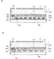
本発明の無線チップの一実施の形態を図1に示す。図1(A)及び図1(B)は無線チップの断面図である。
(Embodiment 1)
One embodiment of a wireless chip of the present invention is shown in FIG. 1A and 1B are cross-sectional views of the wireless chip.
本実施の形態の無線チップは、薄膜トランジスタを有する層102と、アンテナ103とが異方性導電接着材104によって固着される。また、薄膜トランジスタを有する層102の接続端子107とアンテナの給電体層113とが異方性導電接着材104に分散される導電性粒子109で電気的に接続される。又、図示しないが、薄膜トランジスタを有する層のグラウンド配線と、アンテナの接地体として機能する導電層とが異方性導電接着材104に分散される導電性粒子109で電気的に接続される。
In the wireless chip of this embodiment, the thin
薄膜トランジスタを有する層102は、絶縁層105上に形成される薄膜トランジスタ106、薄膜トランジスタ106上に形成される絶縁層108、絶縁層108の表面に露出し、且つ薄膜トランジスタ106と接続する接続端子107で形成される。なお、薄膜トランジスタを有する層102は、薄膜トランジスタ106のほかに薄膜で形成される抵抗素子、コンデンサ等を有してもよい。
The
薄膜トランジスタを有する層は、アンテナ103と同様の面積を有することが好ましく、数mm×数mm〜数十mm×数十mmであることが好ましい。また、薄膜トランジスタを有する層の厚さは、数μm〜数十μm、代表的には1μm以上10μm以下、好ましくは2μm以上5μm以下である。
The layer having a thin film transistor preferably has an area similar to that of the
絶縁層105は、薄膜トランジスタを有する層102の保護層として機能する。絶縁層105は、スパッタリング法やプラズマCVD法等の公知の手段により、酸化珪素、酸化窒化珪素、窒化酸化珪素、窒化珪素等で形成される。
The insulating
薄膜トランジスタ106の一態様について、図16を参照して説明する。図16(A)はトップゲート型の薄膜トランジスタを適用する一例を示している。絶縁層105上に薄膜トランジスタ106が設けられている。薄膜トランジスタ106は、絶縁層105に半導体層1302、ゲート絶縁層として機能することができる絶縁層1303が設けられている。絶縁層1303の上には、半導体層1302に対応してゲート電極1304が形成され、その上層に保護層として機能する絶縁層1305、層間絶縁層として機能する絶縁層1306が設けられている。さらにその上層に、保護層として機能する絶縁層を形成しても良い。
One mode of the
半導体層1302は、結晶構造を有する半導体で形成される層であり、非単結晶半導体若しくは単結晶半導体を用いることができる。特に、非晶質若しくは微結晶質の半導体を、レーザ光の照射により結晶化させた結晶性半導体、加熱処理により結晶化させた結晶性半導体、加熱処理とレーザ光の照射を組み合わせて結晶化させた結晶性半導体を適用することが好ましい。加熱処理においては、シリコン半導体の結晶化を助長する作用のあるニッケルなどの金属元素を用いた結晶化法を適用することができる。
The
レーザ光を照射して結晶化する場合には、連続発振レーザ光の照射若しくは繰り返し周波数が10MHz以上であって、パルス幅が1ナノ秒以下、好ましくは1乃至100ピコ秒である高繰返周波数超短パルス光を照射することによって、結晶性半導体が溶融した溶融帯を、当該レーザ光の照射方向に連続的に移動させながら結晶化を行うことができる。このような結晶化法により、大粒径であって、結晶粒界が一方向に延びる結晶性半導体を得ることができる。キャリアのドリフト方向を、この結晶粒界が延びる方向に合わせることで、トランジスタにおける電界効果移動度を高めることができる。例えば、400cm2/V・sec以上を実現することができる。 In the case of crystallization by irradiating with laser light, high repetition frequency with continuous wave laser light irradiation or repetition frequency of 10 MHz or more and pulse width of 1 nanosecond or less, preferably 1 to 100 picoseconds. By irradiating with ultrashort pulse light, crystallization can be performed while continuously moving the molten zone in which the crystalline semiconductor is melted in the irradiation direction of the laser light. By such a crystallization method, a crystalline semiconductor having a large particle diameter and a crystal grain boundary extending in one direction can be obtained. By adjusting the carrier drift direction to the direction in which the crystal grain boundary extends, the field-effect mobility in the transistor can be increased. For example, 400 cm 2 / V · sec or more can be realized.
上記結晶化工程を、ガラス基板の耐熱温度(約600℃)以下の結晶化プロセスを用いる場合、大面積ガラス基板を用いることが可能である。このため、基板あたり大量の無線チップを作製することが可能であり、低コスト化が可能である。 When the crystallization process is performed using a crystallization process at a heat resistant temperature (about 600 ° C.) or lower of the glass substrate, a large-area glass substrate can be used. Therefore, a large amount of wireless chips can be manufactured per substrate, and cost can be reduced.
また、ガラス基板の耐熱温度以上の加熱により、結晶化工程を行い、半導体層1302を形成してもよい。代表的には、絶縁性基板に石英基板を用い、非晶質若しくは微結晶質の半導体を700度以上で加熱して半導体層1302を形成する。この結果、結晶性の高い半導体を形成することが可能である。このため、応答速度や移動度などの特性が良好で、高速な動作が可能な薄膜トランジスタを提供することができる。
Alternatively, the
さらには、半導体層1302として、単結晶半導体を用いて形成してもよい。
Further, the
このような単結晶半導体で半導体層が形成されるトランジスタは、応答速度や移動度などの特性が良好なために、高速な動作が可能なトランジスタを提供することができる。また、トランジスタは、その特性のバラツキが少ないために、高い信頼性を実現した無線チップを提供することができる。 Since a transistor in which a semiconductor layer is formed using such a single crystal semiconductor has favorable characteristics such as response speed and mobility, a transistor that can operate at high speed can be provided. In addition, since the transistor has little variation in characteristics, a wireless chip realizing high reliability can be provided.
ゲート電極1304は金属又は一導電型の不純物を添加した多結晶半導体で形成することができる。金属を用いる場合は、タングステン(W)、モリブデン(Mo)、チタン(Ti)、タンタル(Ta)、アルミニウム(Al)などを用いることができる。また、上記した金属を窒化させた金属窒化物を用いることができる。或いは、当該金属窒化物からなる第1層と当該金属から成る第2層とを積層させた構造としても良い。積層構造とする場合には、第1層の端部が第2層の端部より外側に突き出した形状としても良い。このとき第1層を金属窒化物とすることで、バリアメタルとすることができる。すなわち、第2層の金属が、絶縁層1303やその下層の半導体層1302に拡散することを防ぐことができる。
The
ゲート電極1304の側面には、サイドウォール(側壁スペーサ)1308が形成される。サイドウォールは、基板上にCVD法により酸化珪素で形成される絶縁層を形成し、該絶縁層をRIE(Reactive ion etching:反応性イオンエッチング)法により異方性エッチングすることで形成できる。
Sidewalls (sidewall spacers) 1308 are formed on the side surfaces of the
半導体層1302、絶縁層1303、ゲート電極1304などを組み合わせて構成されるトランジスタは、シングルドレイン構造、LDD(低濃度ドレイン)構造、ゲートオーバーラップドレイン構造など各種構造を適用することができる。ここでは、サイドウォールが重畳する半導体層において、低濃度不純物領域1310が形成されるLDD構造の薄膜トランジスタを示す。また、シングルゲート構造、等価的には同電位のゲート電圧が印加されるトランジスタが直列に接続された形となるマルチゲート構造、半導体層を上下にゲート電極で挟むデュアルゲート構造を適用することができる。
Various structures such as a single drain structure, an LDD (lightly doped drain) structure, and a gate overlap drain structure can be applied to a transistor including the
絶縁層1306は、酸化シリコン及び酸化窒化シリコンなどの無機絶縁材料、又はアクリル樹脂及びポリイミド樹脂などの有機絶縁材料で形成する。スピン塗布やロールコーターなど塗布法を用いて絶縁層を形成する場合には、有機溶媒中に溶かされた絶縁膜材料を塗布した後、熱処理により絶縁層を形成される酸化シリコンを形成することもできる。例えば、シロキサン結合を含む塗布膜を形成しておいて、200乃至400度での熱処理により酸化シリコンで形成される形成可能な絶縁層を形成することができる。絶縁層1306を、塗布法で形成される絶縁層やリフローにより平坦化した絶縁層を用いることで、その層上に形成する配線の断線を防止することができる。また、多層配線を形成する際にも有効に利用することができる。
The insulating
絶縁層1306の上に形成される配線1307は、ゲート電極1304と同じ層で形成される配線と交差して設けることが可能であり、多層配線構造を形成している。絶縁層1306と同様に機能を有する絶縁層を複数積層して、その層上に配線を形成することで多層配線構造を形成することができる。配線1307はチタン(Ti)とアルミニウム(Al)の積層構造、モリブデン(Mo)とアルミニウム(Al)との積層構造など、アルミニウム(Al)のような低抵抗材料と、チタン(Ti)やモリブデン(Mo)などの高融点金属材料を用いたバリアメタルとの組み合わせで形成することが好ましい。
The
図18(B)は、ボトムゲート型の薄膜トランジスタを適用する一例を示している。絶縁性基板上に絶縁層105が形成され、その上に薄膜トランジスタ106が設けられている。薄膜トランジスタ106には、ゲート電極1304、ゲート絶縁層として機能する絶縁層1303、半導体層1302、チャネル保護層1309、保護層として機能する絶縁層1305、層間絶縁層として機能する絶縁層1306が設けられている。さらにその上層には、保護層として機能する絶縁層を形成しても良い。配線1307は、絶縁層1305の層上若しくは絶縁層1306の層上に形成することができる。なお、ボトムゲート型の薄膜トランジスタの場合は、絶縁層105が形成されなくともよい。
FIG. 18B illustrates an example in which a bottom-gate thin film transistor is applied. An insulating
図1(A)に示す絶縁層108は、絶縁層1306と同様の手法により形成される。また、接続端子107は、配線1307と同様の手法により形成される。また、配線の最上表面に、金、銀、銅、パラジウム、又は白金から選ばれた一元素、若しくは複数の元素で形成される層を、印刷法、メッキ法、スパッタリング法等を用いて設けてもよい。
The insulating
薄膜トランジスタを有する層102は、基板上に剥離層を設け、剥離層上に薄膜トランジスタを有する層102を形成した後、薄膜トランジスタを有する層102を剥離層から剥離し、アンテナ103上に異方性導電接着材104を介して貼り合わせる。なお剥離方法としては、(1)耐熱性の高い基板と薄膜トランジスタを有する層の間に金属酸化膜を設け、当該金属酸化膜を結晶化により脆弱化して、当該薄膜トランジスタを有する層を剥離する方法、(2)耐熱性の高い基板と薄膜トランジスタを有する層の間に水素を含む非晶質珪素膜を設け、レーザ光の照射またはエッチングにより当該非晶質珪素膜を除去することで、当該薄膜トランジスタを有する層を剥離する方法、(3)薄膜トランジスタが形成された耐熱性の高い基板(ガラス基板、シリコン基板等)を機械的に削除又は溶液やNF3、BrF3、ClF3等のフッ化ハロゲンガスによるエッチングで除去する方法、(4)耐熱性の高い基板と薄膜トランジスタを有する層の間に剥離層及び金属酸化膜を設け、当該金属酸化膜を結晶化により脆弱化し、剥離層の一部を溶液やNF3、BrF3、ClF3等のフッ化ハロゲンガスによりエッチングで除去した後、脆弱化された金属酸化膜において物理的に剥離する方法、(5)基板に、耐熱性を有する基板を用い、当該基板と絶縁層との間に剥離層及び金属酸化膜を設け、絶縁層上に第2の薄膜トランジスタを有する層131を形成すると共に金属酸化膜を脆弱化し、第2の薄膜トランジスタを有する層131の絶縁層の一部にレーザ光を照射して、開口部(剥離層の一部を露出する開口部)を形成した後、基体を第2の薄膜トランジスタを有する層131上に貼り付け、脆弱化された金属酸化膜を用いて物理的に基板から第2の薄膜トランジスタを有する層131を剥離する方法等を適宜用いればよい。
The
また、半導体層1302として、単結晶半導体を用いて形成する場合は、第1の単結晶半導体層と、絶縁層と、第2の単結晶半導体層が順に積層された基板(SIMOX(Separation by Implanted Oxygen基板)を用い、第1の単結晶半導体層をチャネル領域としたトランジスタを作製した後、第2の単結晶半導体層をエッチングして除去したのち、アンテナ103上に異方性導電接着材104を介して貼り合わせる。第2の単結晶半導体層のエッチング方法としては、砥石等の研削研磨装置を用いた研磨、エッチング剤を用いたドライエッチング又はウエットエッチング、さらには研削研磨装置とエッチング剤を併用して行ってもよい。エッチング剤は、ウエットエッチングであれば、フッ酸を水やフッ化アンモニウムで希釈した混液、フッ酸と硝酸の混液、フッ酸と硝酸と酢酸の混液、過酸化水素と硫酸の混液、過酸化水素とアンモニア水との混液、過酸化水素と塩酸の混液等を用いる。また、ドライエッチングであれば、フッ素等のハロゲン系の原子や分子を含む気体、又はハロゲン系の原子や分子と共に酸素を含む気体を用いる。好ましくは、フッ化ハロゲン又はハロゲン化合物を含む気体又は液体を使用する。例えば、フッ化ハロゲンを含む気体として三フッ化塩素(ClF3)を用いるとよい。
In the case where the
異方性導電接着材104は、導電性粒子(粒径数nm〜数μm程度)が分散された接着性の有機樹脂であり、有機樹脂としてエポキシ樹脂、フェノール樹脂等が挙げられる。また、導電性粒子は、金、銀、銅、パラジウム、又は白金から選ばれた一元素、若しくは複数の元素で形成される。また、これらの元素の多層構造を有する粒子でも良い。更には、樹脂で形成された粒子の表面に、金、銀、銅、パラジウム、又は白金から選ばれた一金属、若しくは複数の金属で形成される薄膜がコーティングされた導電性粒子を用いてもよい。
The anisotropic
アンテナ103は、誘電体層110と、誘電体層の一表面に形成される第1の導電層111と、誘電体層を介して第1の導電層111に対向し、且つ誘電体層の他表面に形成される第2の導電層112と、給電体層113とを有する。このような構造を有するアンテナを、以下パッチアンテナと示す。第1の導電層111は、放射電極として機能する。また、第2の導電層112は接地体として機能する。給電体層113は、第1の導電層111と第2の導電層112と接触しないように設けられている。また、給電体層113を介して、アンテナから薄膜トランジスタで構成される回路、又は薄膜トランジスタで構成される回路からアンテナへ給電が行われる。なお、給電体層の代わりに給電点を用いて給電を行ってもよい。
The
本実施の形態では、接続端子107と給電体層113とが、異方性導電接着材104の導電性粒子109を介して電気的に接続されている。なお、図示しないが薄膜トランジスタで形成される回路の接地電極とアンテナ103の第2の導電層112とが同様に導電性粒子109を介して電気的に接続されている。
In the present embodiment, the
ここで、アンテナ103として用いるパッチアンテナの構造について説明する。
Here, the structure of the patch antenna used as the
パッチアンテナの誘電体層110は、セラミックス、有機樹脂、又はセラミックスと有機樹脂の混合物等で形成することができる。セラミックスの代表例としては、アルミナ、ガラス、フォルステライト等が挙げられる。さらには、複数のセラミックスを混合して用いてもよい。また、高い誘電率を得るためには、誘電体層110を、強誘電体材料で形成することが好ましい。強誘電体材料の代表例としては、チタン酸バリウム(BaTiO3)、チタン酸鉛(PbTiO3)、チタン酸ストロンチウム(SrTiO3)、ジルコン酸鉛(PbZrO3)、ニオブ酸リチウム(LiNbO3)、チタン酸ジルコン鉛(PZT)等が挙げられる。さらには、複数の強誘電体材料を混合して用いてもよい。
The
また、有機樹脂としては、熱硬化性樹脂又は熱可塑性樹脂を適宜用いる。有機樹脂の代表例としては、エポキシ樹脂、フェノール樹脂、ポリブタジエン樹脂、ビスマレイミドトリアジン樹脂、ビニルベンジル、ポリフマレート、フッ化樹脂等の樹脂材料を用いることができる。さらには、複数の有機樹脂材料を混合して用いてもよい。 As the organic resin, a thermosetting resin or a thermoplastic resin is used as appropriate. As typical examples of organic resins, resin materials such as epoxy resins, phenol resins, polybutadiene resins, bismaleimide triazine resins, vinyl benzyl, polyfumarate, and fluorinated resins can be used. Furthermore, a plurality of organic resin materials may be mixed and used.
誘電体層110がセラミックスと有機樹脂の混合物で形成される場合、粒子状のセラミックスの粒子を有機樹脂に分散させて形成することが好ましい。このとき、誘電体層110に対して粒子状のセラミックスの含有量は、20%体積%以上60体積%以下が好ましい。また、セラミックスの粒径は1〜50μmが好ましい。
When the
誘電体層110の比誘電率は2.6〜150、好ましくは、2.6〜40であることが望ましい。比誘電率の高い強誘電体材料を用いることで、パッチアンテナの容積を小さくすることが可能である。
The relative dielectric constant of the
パッチアンテナの第1の導電層111、第2の導電層112、給電体層113は、金、銀、銅、パラジウム、白金、アルミニウムから選ばれる金属、又は合金等を用いることができる。また、パッチアンテナの第1の導電層111、第2の導電層112、給電体層113は、印刷法、メッキ法を用いて形成することができる。また、誘電体層に蒸着法、スパッタリング法等で導電膜を成膜した後、当該導電膜の一部分をエッチングして各導電層を形成することができる。
For the first
パッチアンテナの大きさとしては、数mm×数mm〜数十mm×数十mmであることが好ましい。代表的には、7mm×7mm〜12mm×12mmである。また、パッチアンテナの厚さは、1mm〜15mm、代表的には1.5mm〜5mmである。また、パッチアンテナの形状は、矩形の平板体が好ましいがこれに限定されるものではない。円形の平板体を用いることも可能である。 The size of the patch antenna is preferably several mm × several mm to several tens mm × several tens mm. Typically, it is 7 mm × 7 mm to 12 mm × 12 mm. The patch antenna has a thickness of 1 mm to 15 mm, typically 1.5 mm to 5 mm. Further, the shape of the patch antenna is preferably a rectangular flat plate, but is not limited thereto. It is also possible to use a circular flat plate.
パッチアンテナについて図7を用いて説明する。 The patch antenna will be described with reference to FIG.
図7(A)は、放射電極として機能する第1の導電層202と、誘電体層201と、接地体として機能する第2の導電層203と、給電点204と、第1の導電層、誘電体層、及び第2の導電層に設けられたスルーホールに形成され、給電点に接続する給電体を有するパッチアンテナである。なお、給電体は、給電点において第1の導電層と接続するが、第2の導電層とは接続しない。放射電極として機能する第1の導電層202が、円形であり、且つ点対称となる2つの領域において、縮退分離素子205がある場合、円偏波のアンテナとなる。また、第1の導電層202が円形の場合、パッチアンテナは直偏波のアンテナとなる。
FIG. 7A illustrates a first
図7(B)は、放射電極として機能する第1の導電層212と、誘電体層211と、接地体として機能する第2の導電層213と、給電点214と、第1の導電層、誘電体層、及び第2の導電層に設けられたスルーホールに形成され、給電点に接続する給電体を有するパッチアンテナである。なお、給電体は、給電点において第1の導電層と接続するが、第2の導電層とは接続しない。放射電極として機能する第1の導電層212は、矩形であり、且つ点対称となる2つの角部において、縮退分離素子215がある場合、円偏波のアンテナとなる。また、第1の導電層212が矩形の場合、パッチアンテナは直偏波のアンテナとなる。
FIG. 7B illustrates a first
図7(C)は、放射電極として機能する第1の導電層222と、誘電体層221と、接地体として機能する第2の導電層223と、給電体層224とを有するパッチアンテナである。放射電極として機能する第1の導電層222は、矩形であり、且つ点対称となる2つの角部において、縮退分離素子225を有する円偏波のアンテナである。また、第1の導電層222が縮退分離素子225を有さない矩形の場合、パッチアンテナは直偏波のアンテナとなる。放射電極として機能する第1の導電層222と給電体層224とは、ギャップを介して容量的に結合されている。また、給電体層224は誘電体層の側面に形成されているため、表面実装が可能である。
FIG. 7C illustrates a patch antenna including a first
図7(A)〜図7(C)に示すパッチアンテナは、誘電体層201、211、221の一方の面に接地体として機能する第2の導電層203、213、223が設けられているため、第1の導電層202、212、222側に指向性を有し、第1の導電層側に電波を放射する。
The patch antenna shown in FIGS. 7A to 7C is provided with second
図7(D)は、放射電極として機能する第1の導電層242と、誘電体層241と、接地体として機能する第2の導電層243と、給電体層244とを有するパッチアンテナである。また、図7(D)に示すように、第1の導電層242において、対角線上に直交スリットが形成されている。すなわち、放射電極として機能する第1の導電層242には、十字の切欠きが設けられている。このため、誘電体層241が十字に露出している。放射電極として機能する第1の導電層242と給電体層244とは、ギャップを介して容量的に結合されている。このような形状のパッチアンテナの代表例としては、CABPB1240、CABPB0730、CABPB0715(TDK製)が挙げられる。また、給電体層244は誘電体層の側面に形成されているため、表面実装が可能である。このような構造のパッチアンテナは、放射電極の直交スリットにより無指向性であるため、全方向へ電波を放射することが可能である。このため、搭載場所や設置角度を選ばなくとも良い。このため、電子機器の設計の自由度を広げることが可能である。
FIG. 7D illustrates a patch antenna including a first
また、図7に示すパッチアンテナ以外にも公知のパッチアンテナを用いることが可能である。 In addition to the patch antenna shown in FIG. 7, a known patch antenna can be used.
特に、円偏波のパッチアンテナを用いることで、GPS(Global Positioning System(1.5GHz))、衛星デジタル放送(2.6GHz)等の衛星送受信、無線LAN(Local Area Network)(2.4GHz、5.2GHz)、Bluetooth(商標)(2.4GHz)、UWB(Ultra Wide Band:超広帯域無線)(3〜10GHz)等のPAN(パーソナルエリアネットワーク)の送受信、第3世代のデータ通信、パケット通信等の送受信を行うことができる。 In particular, by using a circularly polarized patch antenna, satellite transmission / reception such as GPS (Global Positioning System (1.5 GHz)) and satellite digital broadcasting (2.6 GHz), wireless LAN (Local Area Network) (2.4 GHz, PAN (Personal Area Network) such as 5.2 GHz), Bluetooth (trademark) (2.4 GHz), UWB (Ultra Wide Band) (3-10 GHz), third generation data communication, packet communication Etc. can be transmitted and received.
なお、図1(B)に示すように、薄膜トランジスタを有する層120は、複数の薄膜トランジスタを有する層121〜123が複数積層されていてもよい。具体的には、第1の薄膜トランジスタを有する層121上に、第2の薄膜トランジスタを有する層122が形成される。第2の薄膜トランジスタを有する層122上に第3の薄膜トランジスタを有する層123が形成される。第3の薄膜トランジスタを有する層123において、薄膜トランジスタ上に絶縁層127が形成される。また、絶縁層127の表面に、第1の薄膜トランジスタを有する層乃至第3の薄膜トランジスタを有する層のいずれかの薄膜トランジスタに接続する接続端子126が形成される。
Note that as illustrated in FIG. 1B, the
なお、第1の薄膜トランジスタを有する層121において、薄膜トランジスタ上に第1の絶縁層124が形成される。第1の絶縁層124によって、第1の薄膜トランジスタを有する層121の薄膜トランジスタと、第2の薄膜トランジスタを有する層122の薄膜トランジスタとが絶縁される。また、第2の薄膜トランジスタを有する層122において、薄膜トランジスタ上に第2の絶縁層125が形成される。第2の絶縁層125によって、第2の薄膜トランジスタを有する層122の薄膜トランジスタと、第3の薄膜トランジスタを有する層123の薄膜トランジスタとが絶縁される。また、第3の薄膜トランジスタを有する層123において、薄膜トランジスタ上に第3の絶縁層127が形成される。第3の絶縁層127によって、第3の薄膜トランジスタを有する層123の薄膜トランジスタと、接続端子とが絶縁される。
Note that in the
図1(B)において、第1の薄膜トランジスタを有する層乃至第3の薄膜トランジスタを有する層を用いて、薄膜トランジスタを有する層120と示したが、これに限れられるものではなく、2つの薄膜トランジスタを有する層で構成してもよい。また4つ以上の薄膜トランジスタを有する層で構成してもよい。
In FIG. 1B, the first thin film transistor layer to the third thin film transistor layer are used as the
また、図3(A)に示すように、薄膜トランジスタを有する層102は、有機樹脂層101を介して可撓性を有する基板100に固着されていてもよい。可撓性を有する基板100の代表例としては、薄くて軽いプラスチック基板を用いることが好ましく、代表的には、PET(ポリエチレンテレフタレート)、PEN(ポリエチレンナフタレート)、PES(ポリエーテルサルホン)、ポリプロピレンポリカーボネート、ポリエーテルイミド、ポリフェニレンサルファイド、ポリフェニレンオキサイド、ポリサルホン、ポリフタールアミド等からなる基板を用いることができる。また、可撓性を有する基板100として、離型紙等のフィルムがコーティングされた紙を用いることができる。
As shown in FIG. 3A, the
また、有機樹脂層101の代表例としては、熱硬化型接着剤、重合型接着剤、感圧型接着剤、ホットメルト接着剤等の反応型接着剤が硬化した有機樹脂を用いることが好ましく、代表的にはフェノール樹脂、エポキシ樹脂、シリコン樹脂、アクリル樹脂、ポリエステル樹脂、珪素樹脂等が挙げられる。
As a typical example of the
なお、可撓性を有する基板100に接着性樹脂層が設けられている場合、薄膜トランジスタを有する層102に可撓性を有する基板を固着することが可能である。
Note that in the case where an adhesive resin layer is provided over the
なお、ここでは、図1(A)の薄膜トランジスタを有する層102に有機樹脂を介して可撓性を有する基板が設けられた無線チップを図示したが、これに限定されるものではなく、図1(B)に示すような複数の薄膜トランジスタを有する層に有機樹脂を介して可撓性を有する基板を設けてもよい。
Note that here, a wireless chip in which a flexible substrate is provided via an organic resin on the
また、図3(B)に示すように、可撓性を有する基板100上に形成された薄膜トランジスタを有する層141と、アンテナ103とが異方性導電接着材104で固着されていてもよい。
3B, the
薄膜トランジスタを有する層141の表面に形成される接続端子107と給電体層113とが、異方性導電接着材の導電性粒子109を介して電気的に接続されている。なお、図示しないが薄膜トランジスタで形成される回路の接地電極とアンテナの第2の導電層112とが同様に導電性粒子を介して電気的に接続されている。
A
可撓性を有する基板100は、ガラス基板等の非可撓性基板と比較して耐熱温度が低い。このため、薄膜トランジスタは、有機半導体を用いて形成することが好ましい。有機半導体を用いて形成される薄膜トランジスタを有する層は、可撓性を有する基板100上に薄膜トランジスタ142が形成され、薄膜トランジスタ142を覆う絶縁層108が形成されている。また、薄膜トランジスタを有する層141の表面には、薄膜トランジスタ142の配線に接続する接続端子107が形成されている。
The
ここで、有機半導体を用いる薄膜トランジスタの構造について、図17を参照して説明する。図17(A)は、スタガ型の薄膜トランジスタを適用する一例を示している。可撓性を有する基板1401上に薄膜トランジスタ142が設けられている。薄膜トランジスタ142は、ゲート電極1402、ゲート絶縁膜として機能する絶縁層1403、ゲート電極及びゲート絶縁膜として機能する絶縁層と重畳する半導体層1404、半導体層1404に接続する配線1405、1406が形成されている。なお、半導体層は、ゲート絶縁膜として機能する絶縁層1403と配線1405、1406に接する。
Here, a structure of a thin film transistor using an organic semiconductor is described with reference to FIGS. FIG. 17A illustrates an example in which a staggered thin film transistor is applied. A
ゲート電極1402は、ゲート電極1304と同様の材料及び手法により、形成することができる。また、微粒子を含む組成物の液滴を微細な孔から吐出して所定の形状のパターンを形成する方法(以下、本明細書では液滴吐出法という)を用い、乾燥及び焼成してゲート電極1402を形成することができる。また、可撓性を有する基板上に、微粒子を含むペーストを印刷法により印刷し、乾燥及び焼成してゲート電極1402を形成することができる。微粒子の代表例としては、金、銅、金と銀の合金、金と銅の合金、銀と銅の合金、金と銀と銅の合金のいずれかを主成分とする微粒子でもよい。また、インジウム錫酸化物(ITO)などの導電性酸化物を主成分とする微粒子でもよい。
The
ゲート絶縁膜として機能する絶縁層1403は、絶縁層1303と同様の材料及び手法により形成することができる。但し、有機溶媒中に溶かされた絶縁膜材料を塗布した後、熱処理により絶縁層を形成する場合、熱処理温度が可撓性を有する基板の耐熱温度より低い温度で行う。
The insulating
半導体層1404は、多環芳香族化合物、共役二重結合系化合物、フタロシアニン、電荷移動型錯体等が挙げられる。例えばアントラセン、テトラセン、ペンタセン、6T(ヘキサチオフェン)、TCNQ(テトラシアノキノジメタン)、PTCDA(ペリレンカルボン酸無水化物)、NTCDA(ナフタレンカルボン酸無水化物)などを用いることができる。また、具体的な有機高分子化合物材料は、π共役系高分子、カーボンナノチューブ、ポリビニルピリジン、フタロシアニン金属錯体等が挙げられる。特に骨格が共役二重結合から構成されるπ共役系高分子である、ポリアセチレン、ポリアニリン、ポリピロール、ポリチエニレン、ポリチオフェン誘導体、ポリ(3アルキルチオフェン)、ポリパラフェニレン誘導体又はポリパラフェニレンビニレン誘導体を用いると好ましい。
Examples of the
また、有機半導体膜の成膜方法としては、基板に膜厚の均一な膜が形成できる方法を用いればよい。膜厚は1nm以上1000nm以下、好ましくは10nm以上100nm以下が望ましい。具体的な方法としては、蒸着法、塗布法、スピンコーティング法、バーコート法、溶液キャスト法、ディップ法、スクリーン印刷法、ロールコーター法又は液滴吐出法を用いることができる。 As a method for forming the organic semiconductor film, a method that can form a film with a uniform thickness on the substrate may be used. The film thickness is 1 nm to 1000 nm, preferably 10 nm to 100 nm. As a specific method, an evaporation method, a coating method, a spin coating method, a bar coating method, a solution casting method, a dip method, a screen printing method, a roll coater method, or a droplet discharge method can be used.
配線1405、1406は、ゲート電極1402と同様の材料及び手法により形成することが可能である。
The
図17(B)は、コプレナー型の薄膜トランジスタを適用する一例を示している。可撓性を有する基板1401上に薄膜トランジスタ142が設けられている。薄膜トランジスタ142は、ゲート電極1402、ゲート絶縁膜として機能する絶縁層1403、配線1405、1406、ゲート電極及びゲート絶縁層として機能する絶縁層1403に重畳する半導体層1404が形成されている。また、配線1405、1406は、ゲート絶縁層として機能する絶縁層1403及び半導体層1404に接する。
FIG. 17B illustrates an example in which a coplanar thin film transistor is used. A
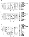
ここで、本発明の無線チップの構成について、図9、図10を参照して説明する。図9(A)に示すように、本発明の無線チップ20は、非接触でデータを交信する機能を有し、電源回路11、クロック発生回路12、データ復調・変調回路13、他の回路を制御する制御回路14、インターフェイス回路15、記憶回路16、バス17、アンテナ18を有する。
Here, the structure of the wireless chip of the present invention will be described with reference to FIGS. As shown in FIG. 9A, the
また、図9(B)に示すように、本発明の無線チップ20は、非接触でデータを交信する機能を有し、電源回路11、クロック発生回路12、データ復調・変調回路13、他の回路を制御する制御回路14、インターフェイス回路15、記憶回路16、バス17、アンテナ18の他、中央処理ユニット21を有しても良い。
Further, as shown in FIG. 9B, the
また、図9(C)に示すように、本発明の無線チップ20は、非接触でデータを交信する機能を有し、電源回路11、クロック発生回路12、データ復調・変調回路13、他の回路を制御する制御回路14、インターフェイス回路15、記憶回路16、バス17、アンテナ18、中央処理ユニット21の他、検出素子31、検出制御回路32からなる検出部30を有しても良い。
Further, as shown in FIG. 9C, the
本実施の形態の無線チップは、薄膜トランジスタを有する層102、120、141により、電源回路11、クロック発生回路12、データ復調・変調回路13、他の回路を制御する制御回路14、インターフェイス回路15、記憶回路16、バス17、アンテナ18、中央処理ユニット21の他、検出素子31、検出制御回路32からなる検出部30等を構成することで、小型で多機能を有する無線チップを形成することが可能である。
The wireless chip of this embodiment includes a
電源回路11は、アンテナ18から入力された交流信号を基に、無線チップ20の内部の各回路に供給する各種電源を生成する回路である。クロック発生回路12は、アンテナ18から入力された交流信号を基に、無線チップ20の内部の各回路に供給する各種クロック信号を生成する回路である。データ復調・変調回路13は、リーダライタ19と交信するデータを復調・変調する機能を有する。制御回路14は、記憶回路16を制御する機能を有する。アンテナ18は、リーダライタ19と電磁波或いは電波の送受信を行う機能を有する。リーダライタ19は、無線チップとの交信、制御及びそのデータに関する処理を制御する。なお、無線チップは上記構成に制約されず、例えば、電源電圧のリミッタ回路や暗号処理専用ハードウエアといった他の要素を追加した構成であってもよい。
The
記憶回路16は、DRAM、SRAM、FeRAM、マスクROM、PROM、EPROM、EEPROM、フラッシュメモリ、及び有機メモリから選択される1つ又は複数を有する。
The
なお、有機メモリとは、一対の電極間に有機化合物を有する層を挟んで設けたものをいう。また、有機メモリとは、一対の電極間に有機化合物と無機化合物との混合層を設けたものをいう。有機化合物の代表例としては、電気的作用や光が照射されることにより、結晶状態や導電性、形状が変化する物質を用いる。代表的には、光を吸収することによって酸を発生する化合物(光酸発生剤)をドープした共役高分子、正孔輸送性が高い有機化合物、又は電子輸送性が高い有機化合物を用いることができる。 Note that an organic memory is a memory in which a layer having an organic compound is interposed between a pair of electrodes. An organic memory is a memory in which a mixed layer of an organic compound and an inorganic compound is provided between a pair of electrodes. As a typical example of an organic compound, a substance whose crystal state, conductivity, and shape change when irradiated with an electric action or light is used. Typically, a conjugated polymer doped with a compound that generates acid by absorbing light (a photoacid generator), an organic compound with a high hole-transport property, or an organic compound with a high electron-transport property is used. it can.
また、一対の電極間に有機化合物と無機化合物との混合層を設ける場合には、正孔輸送性の高い有機化合物と電子を受け取りやすい無機化合物とを混合させることが好ましい。また、電子輸送性の高い有機化合物と電子を与えやすい無機化合物とを混合させることが好ましい。このような構成とすることによって、本来内在的なキャリアをほとんど有さない有機化合物に多くのホールキャリアや電子キャリアが発生し、極めて優れたホール注入性・輸送性や電子注入性・輸送性を示す。 In the case where a mixed layer of an organic compound and an inorganic compound is provided between a pair of electrodes, it is preferable to mix an organic compound having a high hole-transport property and an inorganic compound that easily receives electrons. In addition, it is preferable to mix an organic compound having a high electron transporting property and an inorganic compound that easily gives electrons. By adopting such a configuration, many hole carriers and electron carriers are generated in organic compounds that have essentially no inherent carriers, and extremely excellent hole injection properties / transport properties and electron injection properties / transport properties are achieved. Show.
有機メモリは、小型化、薄膜化および大容量化を同時に実現することができるため、記憶回路16を有機メモリで設けることにより、無線チップの小型化、軽量化を達成することができる。
Since the organic memory can simultaneously achieve downsizing, thinning, and large capacity, the wireless chip can be reduced in size and weight by providing the
なお、薄膜トランジスタと同時に、マスクROMを形成することができる。マスクROMは複数のトランジスタで形成する。その際、トランジスタの例えばドレイン領域と接続する配線用のコンタクトホールを開口するか開口しないかによってデータを書き込むことが可能であり、例えば開口する場合は1(オン)、開口しない場合は0(オフ)のデータ(情報)を、メモリセルに書き込むことが可能である。 Note that a mask ROM can be formed at the same time as the thin film transistor. The mask ROM is formed by a plurality of transistors. At that time, data can be written depending on whether or not a contact hole for wiring connected to, for example, a drain region of the transistor is opened. For example, 1 (on) when opened, 0 (off) when not opened. ) Data (information) can be written into the memory cell.
例えば、図1(A)に示す薄膜トランジスタ106上の絶縁層108上に形成されるフォトレジストを露光する工程において、ステッパなどの露光装置を用いてレチクル(フォトマスク)を通して露光する工程の前又は後に、上記コンタクトホールが開口される領域上のフォトレジストに電子ビーム又はレーザを照射する。その後、通常どおり現像、エッチング、フォトレジストの剥離し、配線を形成する工程をおこなう。こうすることで、レチクル(フォトマスク)を交換せずに、電子ビーム又はレーザの照射領域を選択するのみで、上記コンタクトホールを開口するパターンと開口しないパターンをつくり分けることができる。すなわち、電子ビーム又はレーザの照射領域を選択することで、製造時において、半導体装置毎に異なるデータが書き込まれたマスクROMを作製することが可能となる。
For example, in the step of exposing a photoresist formed over the insulating
このようなマスクROMを用いて、製造時に半導体装置ごとの固有識別子(UID:Unique Identifier)等を形成することが可能となる。 Using such a mask ROM, a unique identifier (UID: Unique Identifier) or the like for each semiconductor device can be formed at the time of manufacture.
ここで、中央処理ユニット21の構成について、図10のブロック図を用いて説明する。
Here, the configuration of the
まず、信号がバス17に入力されると、解析回路1003(Instruction Decoderともいう)において信号が解読され、信号が制御信号発生回路1004(CPU Timing Controller)に入力される。信号が入力されると、制御信号発生回路1004から、演算回路(以下、ALU1009と示す)、および記憶回路(以下、レジスタ1010と示す)に制御信号が出力される。
First, when a signal is input to the
なお、制御信号発生回路1004には、ALU1009を制御するALUコントローラ(以下、ACON1005と示す)、レジスタ1010を制御する回路(以下、RCON1006と示す)、タイミングを制御するタイミングコントローラ(以下、TCON1007と示す)、および割り込みを制御する割り込みコントローラ(以下、ICON1008と示す)を含むものとする。
The control signal generation circuit 1004 includes an ALU controller (hereinafter referred to as ACON 1005) that controls the
一方、処理信号がバス17に入力されると、ALU1009、およびレジスタ1010に出力される。そして、制御信号発生回路1004から入力された制御信号に基づく処理(例えば、メモリリードサイクル、メモリライトサイクル、あるいはI/Oリードサイクル、I/Oライトサイクル等)がなされる。
On the other hand, when the processing signal is input to the
なお、レジスタ1010は、汎用レジスタ、スタックポインタ(SP)、プログラムカウンタ(PC)等により構成される。 Note that the register 1010 includes a general-purpose register, a stack pointer (SP), a program counter (PC), and the like.
また、アドレスコントローラー1011は、16ビットのアドレスをバス17へ出力する。
The address controller 1011 outputs a 16-bit address to the
なお、本実施例に示したCPUの構成は、本発明の構成を限定するものではなく、上記構成以外の公知のCPUの構成を用いることも可能である。 The configuration of the CPU shown in this embodiment does not limit the configuration of the present invention, and a known CPU configuration other than the above configuration can also be used.
検出部30は、温度、圧力、流量、光、磁気、音波、加速度、湿度、気体成分、液体成分、その他の特性を物理的又は化学的手段により検出することができる。また、検出部30は、物理量または化学量を検出する検出素子31と当該検出素子31で検出された物理量または化学量を電気信号等の適切な信号に変換する検出制御回路32とを有している。検出素子31としては、抵抗素子、容量結合素子、誘導結合素子、光起電力素子、光電変換素子、熱起電力素子、トランジスタ、サーミスタ、ダイオード、静電容量型素子、圧電素子等で形成することができる。なお、検出部30は複数設けてもよく、この場合、複数の物理量または化学量を同時に検出することが可能である。
The
また、ここでいう物理量とは、温度、圧力、流量、光、磁気、音波、加速度、湿度等を指し、化学量とは、ガス等の気体成分やイオン等の液体に含まれる成分等の化学物質等を指す。化学量としては、他にも、血液、汗、尿等に含まれる特定の生体物質(例えば、血液中に含まれる血糖値等)等の有機化合物も含まれる。特に、化学量を検出しようとする場合には、必然的にある特定の物質を選択的に検出することになるため、あらかじめ検出素子31に検出したい物質と選択的に反応する物質を設けておく。例えば、生体物質の検出を行う場合には、検出素子31に検出させたい生体物質と選択的に反応する酵素、抗体分子または微生物細胞等を高分子等に固定化して設けておくことが好ましい。
The physical quantity here refers to temperature, pressure, flow rate, light, magnetism, sound wave, acceleration, humidity, etc., and the chemical quantity refers to chemicals such as components contained in gas components such as gases and liquids such as ions. It refers to substances. In addition, the chemical amount includes organic compounds such as specific biological substances (for example, blood glucose level contained in blood) contained in blood, sweat, urine and the like. In particular, when a chemical quantity is to be detected, a specific substance is necessarily selectively detected. Therefore, a substance that selectively reacts with a substance to be detected is provided in advance in the
なお、リーダライタと無線チップとの通信時に、検出部30を用いて温度、圧力、流量、光、磁気、音波、加速度、湿度、気体成分、液体成分、その他の特性を検出することができる。また、無線チップに、フィルム状の二次電池を用いても良い。フィルム状の二次電池の代表例として、電解液が浸透したゲルを有する薄型の二次電池を用いることができる。この場合、リーダライタと通信しないときでも、検出部30を用いて上記特性を検出することができる。
Note that the temperature, pressure, flow rate, light, magnetism, sound wave, acceleration, humidity, gas component, liquid component, and other characteristics can be detected using the
本実施の形態の無線チップは、薄膜トランジスタを有する層とアンテナとをほぼ同様の面積で形成することができる。パッチアンテナが、薄膜トランジスタを有する層の保護部材となるため、無線チップの機械的強度が向上する。 In the wireless chip of this embodiment, a layer including a thin film transistor and an antenna can be formed with substantially the same area. Since the patch antenna serves as a protective member for the layer having the thin film transistor, the mechanical strength of the wireless chip is improved.
(実施の形態2)
本発明の無線チップの一実施の形態を図2に示す。図2は無線チップの断面図である。本実施の形態では、異方性導電接着材で固着された複数の薄膜トランジスタを有する層と、パッチアンテナとを有する無線チップの構造について説明する。
(Embodiment 2)
One embodiment of a wireless chip of the present invention is shown in FIG. FIG. 2 is a cross-sectional view of the wireless chip. In this embodiment, a structure of a wireless chip including a layer having a plurality of thin film transistors fixed with an anisotropic conductive adhesive and a patch antenna will be described.
本実施の形態の無線チップは、第1の薄膜トランジスタを有する層102と、第2の薄膜トランジスタを有する層131とが異方性導電接着材133で固着される。
In the wireless chip of this embodiment, the
第1の薄膜トランジスタを有する層102の表面に形成される第1の接続端子と、第2の薄膜トランジスタを有する層131の表面に形成される第2の接続端子とは、異方性導電接着材133中に分散される導電性粒子で電気的に接続される。
The first connection terminal formed on the surface of the
第1の薄膜トランジスタを有する層102及び第2の薄膜トランジスタを有する層131と同様に、第2の薄膜トランジスタを有する層131及び第3の薄膜トランジスタを有する層132が、異方性導電接着材134で固着される。
Similar to the
また、第2の薄膜トランジスタを有する層131の表面に形成される第3の接続端子と、第3の薄膜トランジスタを有する層132の表面に形成される第4の接続端子とは、異方性導電接着材134中に分散される導電性粒子で電気的に接続される。
The third connection terminal formed on the surface of the
第1の薄膜トランジスタを有する層102乃至第3の薄膜トランジスタを有する層132のそれぞれを、プロセッサユニット、電源回路、クロック発生回路、データ復調・変調回路、制御回路、インターフェイス回路、記憶回路、検出回部等のいずれかの回路とすることで、小型で多機能を有する無線チップを形成することが可能である。
Each of the first thin
また、アンテナ103と、第3の薄膜トランジスタを有する層132の表面に形成される第5の接続端子とが、異方性導電接着材の導電性粒子を介して電気的に接続されている。なお、図示しないが薄膜トランジスタで形成される回路の接地電極とアンテナの第2の導電層112とが同様に導電性粒子を介して電気的に接続されている。
In addition, the
図2において、第1の薄膜トランジスタを有する層乃至第3の薄膜トランジスタを有する層が異方性導電接着材により固着される無線チップを示したが、これに限れられるものではなく、2つの薄膜トランジスタを有する層で構成してもよい。また4つ以上の薄膜トランジスタを有する層で構成してもよい。 In FIG. 2, the wireless chip in which the layer including the first thin film transistor to the layer including the third thin film transistor is fixed with an anisotropic conductive adhesive is shown; however, the present invention is not limited to this and includes two thin film transistors. It may consist of layers. Further, it may be composed of a layer having four or more thin film transistors.
また、実施の形態1と同様に、薄膜トランジスタを有する層102は、可撓性を有する基板に固着されていてもよい。
Further, as in Embodiment 1, the
また、本実施の形態と実施の形態1を適宜組み合わせることが可能である。 Further, this embodiment and Embodiment 1 can be combined as appropriate.
本実施の形態の無線チップは、絶縁性基板上に形成された薄膜トランジスタを有する層とアンテナとをほぼ同様の面積で形成することができる。パッチアンテナが、薄膜トランジスタを有する層の保護部材となるため、無線チップの機械的強度が向上する。 In the wireless chip of this embodiment, a layer including a thin film transistor formed over an insulating substrate and an antenna can be formed with substantially the same area. Since the patch antenna serves as a protective member for the layer having the thin film transistor, the mechanical strength of the wireless chip is improved.
また、本実施の形態の無線チップは、薄膜トランジスタを有する層複数がパッチアンテナと固着されるため、高集積化された無線チップである。 In addition, the wireless chip of this embodiment is a highly integrated wireless chip because a plurality of layers including thin film transistors are fixed to a patch antenna.
(実施の形態3)
本発明の無線チップの一実施の形態を図4に示す。図4は無線チップの断面図である。本実施の形態では、薄膜トランジスタを有する層と、受動素子と、パッチアンテナとが、異方性導電接着材や導電層等で固着された無線チップの構造について説明する。
(Embodiment 3)
One embodiment of a wireless chip of the present invention is shown in FIG. FIG. 4 is a cross-sectional view of the wireless chip. In this embodiment, a structure of a wireless chip in which a layer including a thin film transistor, a passive element, and a patch antenna are fixed with an anisotropic conductive adhesive, a conductive layer, or the like will be described.
実施の形態1に示すように薄膜トランジスタを有する層102が形成される。薄膜トランジスタを有する層102と受動素子を有する層150が異方性導電接着材104で固着される。ここでは、受動素子を有する層150を、第1の受動素子151及び第2の受動素子152で示す。また、薄膜トランジスタを有する層102の表面に露出された接続端子107と受動素子を有する層150の第1の接続端子160とが異方性導電接着材104中の導電性粒子で電気的に接続される。
As shown in Embodiment Mode 1, a
また、受動素子を有する層150とアンテナ103とは、導電層171、172で固着される。アンテナ103の給電体層113及び受動素子を有する層150の第2の接続端子168、パッチアンテナの接地体として機能する第2の導電層112及び受動素子の第3の接続端子169は、それぞれ導電層171、172で電気的に接続される。導電層171、172は、導電性ペーストを硬化して形成する。導電性ペーストを硬化した導電層の代表例としては、スズ(Sn)、銀(Ag)、ビスマス(Bi)、銅(Cu)、インジウム(In)、ニッケル(Ni)、アンチモン(Sb)、亜鉛(Zn)の複数を含む合金があげられる。また、導電層171、172の代わりに異方性導電接着材を用いることも可能である。
Further, the
また、第1の受動素子151は、絶縁層154〜157とその間に設けられた導電層162〜164とで、キャパシタ、インダクタ、抵抗のいずれか一つ以上が構成される。第2の受動素子152も同様に、絶縁層157〜160とその間に設けられた導電層165〜167とで、キャパシタ、インダクタ、抵抗のいずれか一つ以上が構成される。
In addition, the first
第1の受動素子151又は第2の受動素子152の絶縁層154〜160の比誘電率は2.6〜40が好ましい。導電層162〜167は、金、銀、銅、アルミニウムなど導電率の高い金属、またはこれらいずれか複数で形成される合金を用いる。
The relative dielectric constant of the insulating
第1の受動素子151、第2の受動素子152の形成方法を以下に示す。酸化アルミニウムと酸化珪素を有するセラミックスを膜厚10〜150μmにシート状としたもの(いわゆるグリーンシート)に、金、銀、銅、アルミニウムなど導電率の高い金属、またはこれらいずれか複数で形成される合金を印刷法により印刷し導電層を形成する。なお、必要であればグリーンシートにスルーホールを形成し、該スルーホールに導電性ペーストを充填して、異なる層に形成される導電層を接続するプラグを形成してもよい。また、グリーンシートは、実施の形態1で示すアンテナ103の誘電体層110を形成するセラミックス、有機樹脂等を適宜混合して形成してもよい。このような導電層が印刷されたグリーンシートを複数積み重ねて熱圧着し、所定の大きさに加工し、800〜1300度で加熱して絶縁層と導電層を焼成して、1の受動素子151、第2の受動素子152を形成することができる。更には、絶縁層の側面に導電層を形成して、各層に形成される導電層を接続されてもよい。
A method for forming the first
キャパシタ、インダクタ、抵抗、配線等の受動素子を複数組み合わせることで、高周波回路を構成するコンデンサ、デュプレクサ、及びローパスフィルタを含むアンテナフロントエンドモジュール、並びにアイソレータ、カプラ、減衰器、及びパワーアンプを含むアイソレータパワーアンプモジュール、VCO(電圧制御発振器)、バンドバスフィルタ(BPF)、積層フィルター、バルントランス、誘電体フィルター、カプラ、共振器等を構成することが可能である。 An antenna front-end module including a capacitor, a duplexer, and a low-pass filter, and an isolator including an isolator, a coupler, an attenuator, and a power amplifier by combining a plurality of passive elements such as a capacitor, an inductor, a resistor, and a wiring. A power amplifier module, a VCO (voltage controlled oscillator), a band-pass filter (BPF), a multilayer filter, a balun transformer, a dielectric filter, a coupler, a resonator, and the like can be configured.
また、薄膜トランジスタを有する層及び受動素子により、高周波回路である電源回路、クロック発生回路、データ復調・変調回路、他の回路を制御する制御回路、インターフェイス回路、記憶回路、バス、アンテナ、及び中央処理ユニット、並びに検出素子及び検出制御回路からなる検出部等を構成する。 In addition, the power supply circuit, clock generation circuit, data demodulation / modulation circuit, control circuit for controlling other circuits, interface circuit, storage circuit, bus, antenna, and central processing by a layer having thin film transistors and passive elements A unit, a detection unit including a detection element and a detection control circuit are configured.
また、実施の形態1と同様に、薄膜トランジスタを有する層102は、有機樹脂層を介して可撓性を有する基板に固着されていてもよい。
Similarly to Embodiment Mode 1, the
本実施の形態と実施の形態1乃至実施の形態3のいずれかを適宜組み合わせることが可能である。 This embodiment and any of Embodiments 1 to 3 can be combined as appropriate.
本実施の形態の無線チップは、厚膜パターンで形成される受動素子と薄膜トランジスタを用いて形成された集積回路からなる。このため、適した機能を有する素子で各回路を高集積化させる。本発明の無線チップを配線基板に実装することで、実装部品数を削減することが可能であるため、配線基板面積の縮小及びそれを有する電子機器の小型化が可能である。
(実施の形態4)
The wireless chip of this embodiment includes an integrated circuit formed using a passive element formed using a thick film pattern and a thin film transistor. For this reason, each circuit is highly integrated with an element having a suitable function. By mounting the wireless chip of the present invention on a wiring board, the number of mounted components can be reduced, so that the wiring board area can be reduced and an electronic device having the wiring board can be downsized.
(Embodiment 4)
本発明の無線チップの一実施の形態を図5に示す。図5は無線チップの断面図である。本実施の形態では、異方性導電接着材で固着した薄膜トランジスタを有する層複数と、受動素子と、パッチアンテナとが、異方性導電接着材や導電層等で固着された無線チップの構造について説明する。 One embodiment of a wireless chip of the present invention is shown in FIG. FIG. 5 is a cross-sectional view of the wireless chip. In this embodiment mode, a wireless chip structure in which a plurality of layers each having a thin film transistor fixed with an anisotropic conductive adhesive, a passive element, and a patch antenna are fixed with an anisotropic conductive adhesive or a conductive layer is used. explain.
実施の形態2と同様に、第1の薄膜トランジスタを有する層102と、第2の薄膜トランジスタを有する層131とが異方性導電接着材133で固着される。
Similarly to Embodiment Mode 2, the
第1の薄膜トランジスタを有する層102の表面に形成される第1の接続端子と、第2の薄膜トランジスタを有する層の表面に形成される第2の接続端子とは、異方性導電接着材133中に分散される導電性粒子で電気的に接続される。
The first connection terminal formed on the surface of the
第1の薄膜トランジスタを有する層102及び第2の薄膜トランジスタを有する層131と同様に、第2の薄膜トランジスタを有する層131及び第3の薄膜トランジスタを有する層132が、異方性導電接着材134で固着される。
Similar to the
また、第2の薄膜トランジスタを有する層131の表面に形成される第3の接続端子と、第3の薄膜トランジスタを有する層の表面に形成される第4の接続端子とは、異方性導電接着材134中に分散される導電性粒子で電気的に接続される。
In addition, the third connection terminal formed on the surface of the
第3の薄膜トランジスタを有する層132と受動素子を有する層150が異方性導電接着材135で固着される。ここでは、実施の形態4と同様に受動素子を有する層150を、第1の受動素子151及び第2の受動素子152で示す。また、第3の薄膜トランジスタを有する層132の表面に露出された接続端子と受動素子を有する層150の第1の接続端子とが異方性導電接着材中の導電性粒子で電気的に接続される。
A
また、実施の形態4と同様に、受動素子を有する層150とアンテナ103とは、導電層171、172で固着される。アンテナ103の給電体層113及び受動素子を有する層150の第2の接続端子168、パッチアンテナの接地体として機能する第2の導電層112及び受動素子の第3の接続端子169は、それぞれ導電層171、172で電気的に接続される。導電層171、172は、導電性ペーストを硬化した導電層を用いる。なお、導電層171、172の代わりに異方性導電接着材を用いることも可能である。
Similarly to
また、実施の形態1と同様に、薄膜トランジスタを有する層102は、可撓性を有する基板に固着されていてもよい。
Further, as in Embodiment 1, the
本実施の形態と実施の形態1乃至実施の形態4のいずれかを適宜組み合わせることが可能である。 This embodiment and any of Embodiments 1 to 4 can be combined as appropriate.
本実施の形態の無線チップは、厚膜パターンで形成される受動素子と薄膜トランジスタを用いて形成された集積回路からなる。このため、適した機能を有する素子で各回路を高集積化することが可能である。本実施の形態の無線チップを配線基板に実装することで、実装部品数を削減することが可能であるため、配線基板面積の縮小及びそれを有する電子機器の小型化が可能である。
(実施の形態5)
The wireless chip of this embodiment includes an integrated circuit formed using a passive element formed using a thick film pattern and a thin film transistor. Therefore, each circuit can be highly integrated with an element having a suitable function. By mounting the wireless chip of this embodiment on a wiring board, the number of mounted components can be reduced, so that the wiring board area can be reduced and an electronic device having the wiring board can be downsized.
(Embodiment 5)
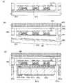
本発明の無線チップの一実施の形態を図6に示す。本実施の形態では、複数のアンテナを有する無線チップの例について示す。図6(A)は無線チップの展開図であり、図6(B)は図6(A)のA−Bにおける断面図である。本実施の形態では、複数のアンテナを有する無線チップにおいて、特に第1の薄膜トランジスタ、第2の薄膜トランジスタ、及び第1の薄膜トランジスタに接続する第1のアンテナを有する層と、パッチアンテナとを有する無線チップの構造について説明する。 An embodiment of a wireless chip of the present invention is shown in FIG. In this embodiment, an example of a wireless chip having a plurality of antennas is described. 6A is a development view of the wireless chip, and FIG. 6B is a cross-sectional view taken along line AB of FIG. 6A. In this embodiment mode, a wireless chip including a plurality of antennas, in particular, a first thin film transistor, a second thin film transistor, a layer having a first antenna connected to the first thin film transistor, and a patch antenna. The structure of will be described.
第1の薄膜トランジスタ186、第2の薄膜トランジスタ185、及び第1の薄膜トランジスタに接続する第1のアンテナを有する層180は、薄膜トランジスタを有する層102上に層間絶縁層182が形成され、層間絶縁層182上に第1のアンテナ181が形成される。第1のアンテナ181上には絶縁層183が形成され、絶縁層183の表面に接続端子184が形成される。
In the first
接続端子184が露出された絶縁層183と第2のアンテナであるアンテナ103とが、異方性導電接着材104により固着される。また、接続端子184とパッチアンテナの給電体層113とが、異方性導電接着材104に分散される導電性粒子で電気的に接続される。接続端子184と第1の薄膜トランジスタ185とが電気的に接続される。また、第2の薄膜トランジスタ186と第1のアンテナ181とが接続される。
The insulating
第1のアンテナ181は、アルミニウム、銅、銀を含む金属材料で形成する。例えば、銅又は銀のペースト状組成物を、スクリーン印刷、オフセット印刷、インクジェット方式の印刷法で形成することができる。また、スパッタリングなどでアルミニウム膜を形成し、エッチング加工により形成しても良い。その他、電解メッキ法、無電解メッキ法を用いて形成しても良い。
The
ここでは、第1のアンテナ181の形状は、図8(A)に示すように方形コイル状である。
Here, the shape of the
第1のアンテナ181の形状について図8を用いて説明する。図8は、層間絶縁層182及びその上に形成されたアンテナを示す上面図である。本実施の形態では、図6(A)及び図8(A)に示すように、第1のアンテナ181は方形コイル状181aであるがこの形状に限定されるものではない。円形コイル状としてもよい。また、図8(B)に示すように方形ループ状181bのアンテナとすることができる。また、円形ループ状アンテナとすることができる。また、図8(C)に示すように直線型ダイポール状181cのアンテナとすることができる。また、曲線型ダイポール状のアンテナとすることができる。
The shape of the
また、図18に示すように、複数のパッチアンテナで薄膜トランジスタを有する層が挟持された無線チップとしてもよい。 Alternatively, as illustrated in FIG. 18, a wireless chip in which a layer having a thin film transistor is sandwiched between a plurality of patch antennas may be employed.
代表的には、図18(A)に示すように、薄膜トランジスタを有する層102の第1の表面に第1の接続端子191が形成される。また、薄膜トランジスタを有する層102の第1の表面と対向する第2の表面に接続端子193が形成される。ここでは、薄膜トランジスタを有する層102は、絶縁層105上に第1の薄膜トランジスタ189及び第2の薄膜トランジスタ190が形成され、当該薄膜トランジスタ上に絶縁層192が形成される。第1の接続端子191は、薄膜トランジスタ189の半導体層に接続し、且つ絶縁層105表面に露出する。また、第2の接続端子193は、薄膜トランジスタ190に接続し、且つ絶縁層192表面に露出する。
Typically, as shown in FIG. 18A, a
第1の接続端子191が露出された絶縁層105と第1のアンテナ103aであるパッチアンテナとが、異方性導電接着材187により固着される。また、第1の接続端子191と第1のアンテナであるパッチアンテナの給電体層113aとが、異方性導電接着材に分散される導電性粒子で電気的に接続される。
The insulating
また、第2の接続端子193が露出された絶縁層192と第2のアンテナ103bであるパッチアンテナとが、異方性導電接着材104により固着される。また、第2の接続端子193と第2のアンテナであるパッチアンテナの給電体層113bとが、異方性導電接着材に分散される導電性粒子で電気的に接続される。
Further, the insulating
第1のアンテナ103aと第2のアンテナ103bとを、周波数の異なるアンテナとすることで、マルチバンド対応が可能な無線チップとなる。さらに、第1のアンテナ103aと第2のアンテナ103bの一方を、無指向性のアンテナとし、他方を指向性のアンテナとすることで、異なる周波数の電波の指向性を使い分けて発信、受信することが可能である。
By using the
さらには、図18(B)に示すように、第1のアンテナ103aであるパッチアンテナ及び第2のアンテナ103bであるパッチアンテナにより、第1乃至第3の薄膜トランジスタ、及び第1の薄膜トランジスタに接続する第3のアンテナを有する層194が挟持された無線チップでもよい。
Further, as shown in FIG. 18B, the first to third thin film transistors and the first thin film transistor are connected to each other by a patch antenna which is the
第1の薄膜トランジスタ189、第2の薄膜トランジスタ190、第3の薄膜トランジスタ195、及び第3の薄膜トランジスタに接続する第3のアンテナ197を有する層194は、1乃至第3の薄膜トランジスタを有する層上に絶縁層192が形成され、絶縁層192上に第3のアンテナ197が形成される。第3のアンテナ197上には絶縁層198が形成され、絶縁層198の表面に接続端子199が形成される。第3のアンテナ197は、第3の薄膜トランジスタ195と導電層196を介して接続される。第3のアンテナ197は、図6及び図8に示す第1のアンテナ181と同様に形成することが可能である。
The
第1の接続端子191が露出された絶縁層105と第1のアンテナ103aであるパッチアンテナとが、異方性導電接着材187により固着される。また、第1の接続端子191と第1のアンテナであるパッチアンテナの給電体層113aとが、異方性導電接着材187に分散される導電性粒子で電気的に接続される。
The insulating
また、第2の接続端子199が露出された絶縁層198と第2のアンテナ103bであるパッチアンテナとが、異方性導電接着材104により固着される。また、第2の接続端子199と第2のアンテナであるパッチアンテナの給電体層113bとが、異方性導電接着材104に分散される導電性粒子で電気的に接続される。
In addition, the insulating
第1のアンテナ103a、第2のアンテナ103b、第3のアンテナ197を、それぞれ周波数の異なるアンテナとすることで、マルチバンド対応が可能な無線チップとなる。さらに、第1のアンテナ103aと第2のアンテナ103bの一方を、無指向性のアンテナとし、他方を指向性のアンテナとすることで、異なる周波数の電波の指向性を使い分けて発信、受信することが可能である。
By using the
本実施の形態と実施の形態1乃至実施の形態5のいずれかを適宜組み合わせることが可能である。 This embodiment and any of Embodiments 1 to 5 can be combined as appropriate.
このように複数のアンテナを設けることで、一つの無線チップで多数の電波を受信、発信することが可能なマルチバンド対応の無線チップを形成することができる。 By providing a plurality of antennas in this way, a multi-band compatible wireless chip capable of receiving and transmitting a large number of radio waves with one wireless chip can be formed.
本実施の形態の無線チップは、厚膜パターンで形成される受動素子と薄膜トランジスタを用いて形成された集積回路からなる無線チップは、適した機能を有する素子で各回路を高集積化することが可能である。本発明の無線チップを配線基板に実装することで、実装部品数を削減することが可能であるため、配線基板面積の縮小及びそれを有する電子機器の小型化が可能である。 In the wireless chip of this embodiment mode, a wireless chip including a passive element formed using a thick film pattern and an integrated circuit formed using a thin film transistor can be highly integrated with each element having an appropriate function. Is possible. By mounting the wireless chip of the present invention on a wiring board, the number of mounted components can be reduced, so that the wiring board area can be reduced and an electronic device having the wiring board can be downsized.
本実施例では、本発明の無線チップの作製方法について図19、図20を用いて説明する。 In this embodiment, a method for manufacturing a wireless chip of the present invention will be described with reference to FIGS.
図19(A)に示すように、基板401の一表面に、絶縁層402、剥離層403を形成する。
As shown in FIG. 19A, an insulating
基板401は、ガラス基板、石英基板、金属基板やステンレス基板の一表面に絶縁層を形成したもの等を用いる。絶縁層402としては公知の手段(スパッタリング法やプラズマCVD法等)により窒化珪素、酸化窒化珪素、窒化酸化珪素等を成膜する。
As the
剥離層403は、公知の手段(スパッタリング法やプラズマCVD法等)により、タングステン(W)、モリブデン(Mo)、チタン(Ti)、タンタル(Ta)、ニオブ(Nb)、ニッケル(Ni)、コバルト(Co)、ジルコニウム(Zr)、亜鉛(Zn)、ルテニウム(Ru)、ロジウム(Rh)、パラジウム(Pd)、オスミウム(Os)、イリジウム(Ir)、珪素(Si)から選択された元素、又は元素を主成分とする合金材料、又は元素を主成分とする化合物材料からなる層を、単層又は積層して形成する。珪素を含む層の結晶構造は、非晶質、微結晶、多結晶のいずれの場合でもよい。
The
剥離層403が積層構造の場合、好ましくは、1層目としてタングステン層、モリブデン層、又はタングステンとモリブデンの混合物を含む層を形成し、2層目として、タングステン、モリブデン、又はタングステンとモリブデンの混合物の酸化物、窒化物、酸化窒化物又は窒化酸化物を形成する。
In the case where the
剥離層403として、タングステンを含む層とタングステンの酸化物を含む層の積層構造を形成する場合、タングステンを含む層を形成し、その上層に酸化珪素を含む層を形成することで、タングステン層と酸化珪素層との界面に、タングステンの酸化物を含む層が形成されることを活用してもよい。さらには、タングステンを含む層の表面を、熱酸化処理、酸素プラズマ処理、オゾン水等の酸化力の強い溶液での処理等を行ってタングステンの酸化物を含む層を形成してもよい。これは、タングステンの窒化物、酸化窒化物及び窒化酸化物を含む層を形成する場合も同様であり、タングステンを含む層を形成後、その上層に窒化珪素層、酸化窒化珪素層、窒化酸化珪素層を形成するとよい。
In the case where a stacked structure of a layer containing tungsten and a layer containing an oxide of tungsten is formed as the
なお、基板401と剥離層403との間に絶縁層402を設けているが、本発明はこの工程に制約されない。基板401に接するように剥離層403を形成してもよい。
Note that although the insulating
ここでは、絶縁層402として厚さ100nmの酸化窒化珪素層をCVD法により形成し、剥離層403として、厚さ30nmのタングステン層をスパッタリング法により形成する。
Here, a silicon oxynitride layer with a thickness of 100 nm is formed as the insulating
次に、図19(B)に示すように、剥離層403を覆うように、下地となる絶縁層404を形成する。絶縁層404は、公知の手段(スパッタリング法やプラズマCVD法等)により、酸化珪素、酸化窒化珪素、窒化珪素、窒化酸化珪素等の単層又は積層で形成する。下地となる絶縁層は、外部から薄膜トランジスタを有する層への不純物の侵入を防止するブロッキング膜として機能する。
Next, as illustrated in FIG. 19B, an insulating
ここでは、下地となる絶縁層404として、CVD法により厚さ50nmの窒化酸化珪素からなる層と、膜厚100nmの酸化窒化珪素からなる層を形成する。
Here, as the insulating
次に、絶縁層404上に、薄膜トランジスタ405を形成する。薄膜トランジスタ405は実施の形態1に示す薄膜トランジスタを適宜用いることができる。ここでは、図16(A)に示すような、絶縁層404上に半導体層、ゲート絶縁層として機能することができる絶縁層、絶縁層1303の上には、半導体層に対応して形成されたゲート電極、その上層に保護層として機能する絶縁層、保護層を介して半導体層に接続される配線で構成されるトップゲート型の薄膜トランジスタを形成する。
Next, a
次に、薄膜トランジスタ405を覆うように、単層又は積層で絶縁層406を形成する。ここでは、絶縁層として、厚さ1.5μmのシロキサンポリマーを塗布し、乾燥及び焼成を行って絶縁層406を形成する。この後、絶縁層406上に、DLC(ダイヤモンドライクカーボン)などの炭素を含む層、窒化珪素を含む層、窒化酸化珪素を含む層等の保護層を形成しても良い。
Next, the insulating
次に、薄膜トランジスタを覆う絶縁層406にコンタクトホールを形成し、接続端子407を形成する。
Next, a contact hole is formed in the insulating
なお、ここでは、絶縁層404、薄膜トランジスタ405、絶縁層406、及び接続端子407を、薄膜トランジスタを有する層408と示す。
Note that here, the insulating
次に、図19(C)に示すように、剥離層403が露出するように、開口部411、412を形成する。開口部411、412は、レーザアブレーションやフォトリソグラフィ法により絶縁層406から絶縁層404まで貫通している。
Next, as shown in FIG. 19C,
ここでは、紫外線レーザから射出されるレーザビームを照射して、開口部411、412を形成する。また、当該開口部411、412によって各無線チップの薄膜トランジスタを有する層となるように分断するために、各チップごとに連続した開口部を設けることが好ましい。
Here, the
次に、開口部411、412にエッチング剤を導入して、図19(D)に示すように、剥離層403の一部を除去する。一部エッチングされた剥離層を、剥離層413と示す。エッチング剤は、ウエットエッチングであれば、フッ酸を水やフッ化アンモニウムで希釈した混液、フッ酸と硝酸の混液、フッ酸と硝酸と酢酸の混液、過酸化水素と硫酸の混液、過酸化水素とアンモア水の混液、過酸化水素と塩酸の混液等を用いる。また、ドライエッチングであれば、フッ素等のハロゲン系の原子や分子を含む気体、又は酸素を含む気体を用いる。好ましくは、エッチング剤として、フッ化ハロゲン又はハロゲン化合物を含む気体又は液体を使用する。
Next, an etchant is introduced into the
ここでは、三フッ化塩素(ClF3)を使用して、剥離層の一部をエッチングする。 Here, a part of the peeling layer is etched using chlorine trifluoride (ClF 3 ).
次に、図19(D)に示すように、薄膜トランジスタを有する層408において絶縁層406、接続端子407の表面と、基体415とを粘着剤414を用いて接着させる。
Next, as illustrated in FIG. 19D, the surface of the insulating
次に、図19(E)に示すように、基板401、絶縁層402、及び剥離層413を、薄膜トランジスタを有する層408から剥がす。
Next, as illustrated in FIG. 19E, the
基体415は、基板401より剛性の高い基板を用いることが好ましい。ここでは、基体415として、石英基板を用いる。粘着剤414としては、剥離可能な粘着剤であり、代表的には紫外線により剥離する紫外線剥離型粘着剤、熱により剥離する熱剥離型粘着剤、水溶性粘着剤や両面粘着テープなどを用いることができる。ここでは、粘着剤414として紫外線剥離型粘着剤を用いる。
As the
このとき、基体415と薄膜トランジスタを有する層418との接着強度は、基板401と絶縁層404との密着強度より高くなるように設定する。そして、絶縁層404上に設けられたトランジスタを有する層408のみを基板401から剥離する。
At this time, the adhesive strength between the base 415 and the layer 418 having a thin film transistor is set to be higher than the adhesive strength between the
次に、図20(A)に示すように、薄膜トランジスタを有する層408の絶縁層404に、接着剤を用いて可撓性を有する基板421を固着する。なお、可撓性を有する基板421に接着性樹層が設けられている場合、接着剤を用いずとも薄膜トランジスタを有する層408の絶縁層404に可撓性を有する基板421を固着することが可能である。ここでは、可撓性を有する基板421として、シリコーン樹脂層を有するPETフィルムとシリカコートを積層させたシート材を利用することができる。
Next, as illustrated in FIG. 20A, a
次に、基体415及び粘着剤414を、薄膜トランジスタを有する層408の絶縁層406及び接続端子407の表面から除去する。
Next, the
ここでは、紫外線を粘着剤414に照射して、粘着剤414を除去する。
Here, the pressure-
次に、図20(B)に示すように、薄膜トランジスタを有する層408の表面、代表的には絶縁層406及び接続端子407の表面に、異方性導電接着材423を用いてパッチアンテナ422を接着する。パッチアンテナ422は、ここでは、放射電極として機能する第1の導電層426、接地体として機能する第2の導電層427、第1の導電層426及び第2の導電層427に挟持される誘電体層428、給電体層429とを有する。また、異方性導電接着材423は、導電性粒子424として銀粒子が分散された接着性のエポキシ樹脂で形成される。
Next, as illustrated in FIG. 20B, the
また、接続端子407及びパッチアンテナ422の給電体層429、図示されない接続端子及び接地体として機能する第2の導電層427を異方性導電接着材423の導電性粒子424で接続する。
In addition, the
その後、可撓性を有する基板421及び薄膜トランジスタを有する層408を個々のアンテナと同様の形状となるように切断する。図20(B)において、切断部分を破線矢印で示す。ここでは、レーザスクライブにより、無線チップを切り出しする。
After that, the
以上の工程により、図20(C)に示すように、可撓性を有する基板421aに固着された薄膜トランジスタを有する層408aと、パッチアンテナ422と、薄膜トランジスタを有する層408a及びパッチアンテナ422を固着する異方性導電接着材423とを有する無線チップ431を形成することが可能である。なお、図20(B)において切断された薄膜トランジスタを有する層408を薄膜トランジスタを有する層408aと示し、切断された可撓性を有する基板421を、可撓性を有する基板421aと示す。
Through the above steps, as illustrated in FIG. 20C, the
なお、本実施例と上記実施の形態のいずれかを適宜組み合わせることが可能である。 Note that this example and any of the above embodiments can be combined as appropriate.
本実施例では、複数のパッチアンテナで薄膜トランジスタを有する層が挟持される無線チップの作製方法について図21、図22を用いて説明する。 In this embodiment, a method for manufacturing a wireless chip in which a layer including a thin film transistor is sandwiched between a plurality of patch antennas will be described with reference to FIGS.
実施例1と同様に、図21(A)に示すように、基板401の一表面に、絶縁層402、剥離層454、455を形成する。ここでは、剥離層454、455は、基板401の一表面に薄膜を形成した後、フォトリソグラフィ法により形成したレジストマスクを用いて薄膜を選択的にエッチングして形成する。ここでは、タングステン膜をスパッタリング法により成膜した後、絶縁層404側に露出する第1の接続端子が形成される領域を除いて、剥離層を形成する。
Similarly to Example 1, as illustrated in FIG. 21A, an insulating
次に絶縁層402及び剥離層454、455上に下地として機能する絶縁層404を形成する。
Next, an insulating
次に、絶縁層404上に、実施例1と同様に、薄膜トランジスタを形成する。ここでは、絶縁層404上に半導体層、ゲート絶縁層として機能することができる絶縁層、絶縁層の上に、半導体層に対応して形成されたゲート電極、その上層に絶縁層450を形成する。この後、絶縁層450上に、DLC(ダイヤモンドライクカーボン)などの炭素を含む層、窒化珪素を含む層、窒化酸化珪素を含む層等の保護層を形成しても良い。
Next, a thin film transistor is formed over the insulating
次に、図21(B)に示すように、絶縁層450に第1のコンタクトホール452を形成する。第1のコンタクトホール452は、半導体層のソース領域及びドレイン領域を露出するコンタクトホールである。次に、第2のコンタクトホール453を形成する。第2のコンタクトホールは、絶縁層450から絶縁層404までの絶縁層をエッチングし、絶縁層402を露出するコンタクトホールである。なお、第2のコンタクトホール453は、剥離層454、455が形成されない領域に設けることが好ましい。
Next, as shown in FIG. 21B, a
次に、図21(C)に示すように、第1のコンタクトホール及び第2のコンタクトホールに配線として機能する導電層461〜466を形成する。なお、配線として機能する導電層461は接続端子としても機能する。
Next, as illustrated in FIG. 21C,
次に、絶縁層450及び配線として機能する導電層461〜466上に絶縁層469を形成し、絶縁層469にコンタクトホールを形成し、接続端子470を形成する。
Next, an insulating
ここでは、半導体層、ゲート絶縁層、ゲート電極、半導体層のソース領域及びドレイン領域に接続する導電層461、462を第1の薄膜トランジスタ455と示す。また、半導体層、ゲート絶縁層、ゲート電極、半導体層のソース領域及びドレイン領域に接続する配線465、466を第2の薄膜トランジスタ456と示す。また、第2の薄膜トランジスタ456の配線466は接続端子470と接続する。
Here, the
ここでは、絶縁層404、第1の薄膜トランジスタ455、第1の薄膜トランジスタ455に接続する導電層461、第2の薄膜トランジスタ456、絶縁層469、及び接続端子470を、薄膜トランジスタを有する層460と示す。
Here, the insulating
次に、図21(D)に示すように、実施例1と同様に、剥離層454、455が露出するように、開口部471、472を形成する。開口部471、472は、レーザアブレーションやフォトリソグラフィ法により絶縁層469から絶縁層404まで貫通している。また、当該開口部471、472によって各無線チップに対応する薄膜トランジスタを形成するために、各無線チップごとに連続した開口部(溝)を設けることが好ましい。
Next, as illustrated in FIG. 21D,
次に、実施例1と同様に、開口部471、472にエッチング剤を導入して、図22(A)に示すように、剥離層454、455の一部を除去する。一部エッチングされた剥離層を、剥離層474、475と示す。
Next, as in Example 1, an etchant is introduced into the
次に、図22(B)に示すように、トランジスタを有する層460において絶縁層469、接続端子470の表面と、基体415とを粘着剤414を用いて接着させる。
Next, as illustrated in FIG. 22B, the surface of the insulating
次に、基板401、絶縁層402、及び剥離層474、475を、薄膜トランジスタを有する層460から剥がす。
Next, the
次に、図22(C)に示すように、薄膜トランジスタを有する層460の第1の表面、代表的には絶縁層404及び導電層461の表面に、第1の異方性導電接着材423aを用いて第1のパッチアンテナ422aを接着する。第1のパッチアンテナ422aは、実施例1のパッチアンテナ422と同様に、放射電極として機能する第1の導電層426a、接地体として機能する第2の導電層427a、第1の導電層426a及び第2の導電層427aに挟持される誘電体層428a、給電体層429aとを有する。また、異方性導電接着材423aは、導電性粒子424aとして銀粒子が分散された接着性のエポキシ樹脂425aで形成される。
Next, as illustrated in FIG. 22C, the first anisotropic conductive adhesive 423a is formed on the first surface of the
また、第1の接続端子464及び第1のパッチアンテナ422aの給電体層429a、図示されない接続端子及び接地体として機能する第2の導電層427aを異方性導電接着材423aの導電性粒子424aで接続する。
In addition, the first connecting
次に、図23(A)に示すように、実施例1と同様に基体415及び粘着剤414を、薄膜トランジスタを有する層460の絶縁層469及び接続端子470の表面から除去する。
Next, as shown in FIG. 23A, the
次に、図23(B)に示すように、薄膜トランジスタを有する層460の第2の表面、代表的には絶縁層469及び接続端子470の表面に、第2の異方性導電接着材423bを用いて第2のパッチアンテナ422bを接着する。第2のパッチアンテナ422bは第1のパッチアンテナ422aと同様に、放射電極として機能する第3の導電層426b、接地体として機能する第4の導電層427b、第3の導電層426b及び第4の導電層427bに挟持される誘電体層428b、給電体層429bとを有する。また、異方性導電接着材423bは、導電性粒子424bである銀粒子が分散された接着性のエポキシ樹脂で形成される。
Next, as illustrated in FIG. 23B, a second anisotropic conductive adhesive 423b is formed on the second surface of the
また、接続端子470及び第2のパッチアンテナ422bの給電体層429b、図示されない接続端子及び接地体として機能する第4の導電層427bを異方性導電接着材423bの導電性粒子424bで接続する。
Further, the
以上の工程により、図23(B)に示すような、第1のパッチアンテナ422aと、第2のパッチアンテナ422bと、薄膜トランジスタを有する層460aと、薄膜トランジスタを有する層408aの第1の表面及び第1のパッチアンテナ422aを固着する第1の異方性導電接着材423aと、薄膜トランジスタを有する層460aの第2の表面及び第2のパッチアンテナ422bを固着する第2の異方性導電接着材423bを有する無線チップ491を形成することが可能である。なお、図23(B)において切断された薄膜トランジスタを有する層460を薄膜トランジスタを有する層460aと示す。
Through the above steps, the
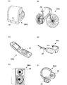
本発明の無線チップの用途は広範にわたるが、例えば、乗物類(自転車3901(図11(B)参照)、自動車等)、食品類、植物類、衣類、生活用品類(鞄3900(図11(A)参照)等)、電子機器、検査装置等の物品に、無線チップ20を設けて使用することができる。また、動物類や人体に設けることができる。電子機器とは、液晶表示装置、EL(Electro Luminescence)表示装置、テレビジョン装置(単にテレビ、テレビ受像機、テレビジョン受像機とも呼ぶ)、携帯電話3902(図11(C)参照)、プリンター、カメラ、パーソナルコンピュータ、イヤホン付ゴーグル3903(図11(D)参照)、スピーカ装置3904(図11(E)参照)、ヘッドホン3905(図11(F)参照)、ナビゲーション装置、ETC(Electoronic Toll Collection:有料道路等の自動料金収受システム)用車載器、電子鍵等を指す。
The wireless chip of the present invention has a wide range of uses. For example, vehicles (bicycles 3901 (see FIG. 11B), automobiles, etc.), foods, plants, clothing, household goods (類 3900 (FIG. 11 ( A) (see A), etc.) can be used by providing the
本発明の無線チップ20を鞄3900、自転車3901等に設けることにより、GPSでこれらの所在を検出することが可能である。この結果、盗難された自転車を見つけ出すことが可能である。また、行方不明者の捜索が容易となる。
By providing the
また、本発明の無線チップ20を携帯電話3902に搭載することにより、情報の送受信及び通話が可能となる。
Further, by mounting the
また、本発明の無線チップをイヤホン付ゴーグル3903、スピーカ装置3904やヘッドホン3905に搭載することにより、オーディオ装置と当該電子機器をコードで接続することなしに、オーディオ装置で再生した音楽を楽しむことが可能である。また、イヤホン付ゴーグル3903に無線チップ20と共に、小型のハードディスク(記憶装置)を設けてもよい。また、無線チップ20に中央処理ユニットを有する場合、オーディオ装置で暗号化した音声信号を、イヤホン付ゴーグル3903、ヘッドホン3905やスピーカ装置3904で受信、復調、増幅することが可能であるため、秘匿性高く音声を聞くことが可能である。また、コードレスのため、イヤホン付ゴーグル3903やヘッドホン3905の装着が容易となり、スピーカ装置3904の設置が容易となる。なお、この場合、イヤホン付ゴーグルやヘッドホン、スピーカ装置は、バッテリーを設けることが好ましい。
In addition, by mounting the wireless chip of the present invention on the goggles with
本発明の無線チップは、プリント基板に実装したり、表面に貼ったり、埋め込んだりして、物品に固定される。例えば、有機樹脂からなるパッケージなら当該有機樹脂に埋め込んだりして、各物品に固定される。また、食品類、植物類、動物類、人体、衣類、生活用品類、電子機器等の物品に本発明の無線チップを設けることにより、検品システムや検査システム等のシステムの効率化を図ることができる。 The wireless chip of the present invention is fixed to an article by being mounted on a printed board, pasted on a surface, or embedded. For example, a package made of an organic resin is embedded in the organic resin and fixed to each article. In addition, by providing the wireless chip of the present invention to foods, plants, animals, human bodies, clothing, daily necessities, electronic devices, etc., it is possible to improve the efficiency of systems such as inspection systems and inspection systems. it can.
次に、本発明の無線チップを実装した電子機器の一態様について図面を参照して説明する。ここで例示する電子機器は携帯電話機であり、筐体2700、2706、パネル2701、ハウジング2702、プリント配線基板2703、操作ボタン2704、バッテリー2705を有する(図13参照)。パネル2701はハウジング2702に脱着自在に組み込まれ、ハウジング2702はプリント配線基板2703に嵌着される。ハウジング2702はパネル2701が組み込まれる電子機器に合わせて、形状や寸法が適宜変更される。プリント配線基板2703には、パッケージングされた複数の半導体装置や本発明の無線チップ2710が実装されている。
Next, one mode of an electronic device on which the wireless chip of the present invention is mounted will be described with reference to the drawings. The electronic device illustrated here is a mobile phone, which includes
パネル2701は、接続フィルム2708を介して、プリント配線基板2703と接続される。上記のパネル2701、ハウジング2702、プリント配線基板2703は、操作ボタン2704やバッテリー2705と共に、筐体2700、2706の内部に収納される。パネル2701が含む画素領域2709は、筐体2700に設けられた開口窓から視認できるように配置されている。
The
なお、筐体2700、2706は、携帯電話機の外観形状を一例として示したものであり、本実施例に係る電子機器は、その機能や用途に応じて様々な態様に変容しうる。
Note that the
ここでは、携帯電話機のデータ復調変調回路に代表される高周波回路のブロック図について、図14を用いて説明する。 Here, a block diagram of a high-frequency circuit typified by a data demodulation and modulation circuit of a mobile phone will be described with reference to FIG.
はじめにアンテナで受信した信号をベースバンドユニットへ送り出す工程を説明する。アンテナ301に入力された受信信号は、デュプレクサ302からローノイズアンプ(LNA)303に入力され、所定の信号に増幅される。ローノイズアンプ(LNA)303に入力された受信信号は、バンドバスフィルタ(BPF)304を経てミキサー305に入力される。このミキサー305には、混成回路306からのRF信号が入力され、RF信号成分がバンドバスフィルタ(BPF)307で除去され、復調される。ミキサー305から出力された受信信号は、SAWフィルター308を経てアンプ309で増幅されたのち、ミキサー310に入力される。ミキサー310には、局部発信回路311から所定の周波数の局部発信信号が入力され、所望の周波数に変換され、アンプ312で所定のレベルに増幅された後、ベースバンドユニット313に送り出す。なお、アンテナ301、デュプレクサ302、及びローパスフィルタ328をアンテナフロントエンドモジュール331と示す。
First, a process of sending a signal received by the antenna to the baseband unit will be described. The received signal input to the
次に、ベースバンドユニットから送出された信号をアンテナで発信する工程について説明する。ベースバンドユニット313から送出された送信信号は、ミキサー321により混成回路306からのRF信号と混合される。この混成回路306には、電圧制御発信回路(VCO)322が接続されており、所定の周波数のRF信号が供給されるようになっている。
Next, a process of transmitting a signal transmitted from the baseband unit with an antenna will be described. The transmission signal transmitted from the
ミキサー321によりRF変調が行われた送信信号は、バンドパスフィルタ(BPF)323を経て、パワーアンプ(PA)324により増幅される。このパワーアンプ(PA)324の出力の一部は、カプラ325から取り出され、減衰器(APC)326で所定のレベルに調整された後、再びパワーアンプ(PA)324に入力され、パワーアンプ(PA)324の利得が一定になるように調整される。カプラ325から送出された送信信号は、逆流防止用のアイソレータ327、ローパスフィルタ328(LPF)、を経て、デュプレクサ302に入力され、これと接続されているアンテナ301から送信される。なお、減衰器(APC)326、パワーアンプ(PA)324、カプラ325、及びアイソレータ327をアイソレータパワーアンプモジュール332と示す。
The transmission signal RF-modulated by the
本発明の無線チップは、上記高周波回路を有するため、部品の数を低減することが可能である。このため、配線基板に実装される部品の数を低減することが可能であるため、配線基板の面積を縮小することが可能である。この結果、携帯電話を小型化することが可能である。 Since the wireless chip of the present invention includes the high-frequency circuit, the number of components can be reduced. For this reason, since the number of components mounted on the wiring board can be reduced, the area of the wiring board can be reduced. As a result, the mobile phone can be reduced in size.
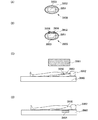
次に、検出した生体の機能データを無線で送信することが可能な検査装置の例について、図12を用いて説明する。図12(A)に示す検査装置3950は、保護層がコーティングされたカプセル3952内に本発明の無線チップ3951が設けられている。カプセル3952と無線チップ3951の間には、充填剤3953が満たされていてもよい。
Next, an example of an inspection apparatus capable of wirelessly transmitting detected biological function data will be described with reference to FIG. In an
図12(B)に示す検査装置3955は、保護層がコーティングされたカプセル3952内に本発明の無線チップ3951が設けられている。また、無線チップの電極3956がカプセル3952の外側に露出している。カプセル3952と無線チップ3951の間には、充填剤3953が満たされていてもよい。
In an
検査装置3950、3955の無線チップ3951は、図9(C)に示すような、検出部を有する無線チップである。検出部において、物理量や化学量を測定して生体の機能データを検出する。また、なお、検出した結果を信号変換して、リーダライタへ送信することが可能である。物理量である圧力、光、音波等を検出する場合、図12(A)に示すような、電極がカプセル3952の外部に露出してない検査装置3950を用いることができる。
The
カプセルの表面に設けられた保護層は、ダイヤモンドライクカーボン(DLC)、窒化珪素、酸化珪素、窒化珪素、酸窒化珪素、又は窒化炭素を含んでいることが好ましい。カプセルや充填材は公知のものを適宜用いる。カプセルに保護層を設けることで、体内でカプセルや無線チップが溶解、変性することを防止することが可能である。 The protective layer provided on the surface of the capsule preferably contains diamond-like carbon (DLC), silicon nitride, silicon oxide, silicon nitride, silicon oxynitride, or carbon nitride. Known capsules and fillers are appropriately used. By providing a protective layer on the capsule, it is possible to prevent the capsule and the wireless chip from being dissolved and denatured in the body.
また、温度、流量、磁気、加速度、湿度、ガス等の気体成分やイオン等の液体成分等の化学物質等を検出する場合、図12(B)に示すような、電極3956がカプセル3952の外部に露出している検査装置3955を用いることが好ましい。
In addition, when detecting chemical substances such as temperature, flow rate, magnetism, acceleration, humidity, gas components such as gas and liquid components such as ions, an
なお、検査装置が体内を撮像する装置である場合、検査装置にLED(Light Emitting Diode)、EL(Electro Luminescence)等の発光装置を設けてもよい。この結果、体内を撮像することが可能である。 Note that in the case where the inspection apparatus is an apparatus that images the inside of the body, the inspection apparatus may be provided with a light emitting device such as an LED (Light Emitting Diode) or an EL (Electro Luminescence). As a result, the inside of the body can be imaged.
なお、検査装置から検出結果のデータをリーダライタに自発的に発信するためには、検出装置に公知のバッテリーを設けてもよい。 In order to spontaneously transmit detection result data from the inspection device to the reader / writer, a known battery may be provided in the detection device.
次に、検査装置の使用方法について説明する。図12(C)に示すように、被験者3962が検査装置3950又は3955を嚥下し、体内腔3963を移動させる。無線チップの検出部が検出した結果を、被験者の近傍に設置されたリーダライタ3961に発信する。リーダライタでは、この結果を受信する。この結果、無線チップを回収せずとも、その場で被験者の生体の機能データを検知することが可能である。また、体内腔及び消化器の様子を撮像することが可能である。
Next, a method for using the inspection apparatus will be described. As shown in FIG. 12C, the subject 3962 swallows the
また、図12(D)に示すように、被験者3962の体内に検査装置3950又は3955を埋め込むことで、無線チップの検出部が検出した結果を、被験者の近傍に設置されたリーダライタ3964に発信する。この場合、被験者の測定対象部に電極3956が接するように検査装置3955体内に埋め込む。リーダライタでは、この結果を受信する。この受信結果を、生体情報管理コンピュータで記録し、処理することで、被験者の生体情報を管理することが可能である。なお、リーダライタ3964をベッド3960に設けることで、身体機能が不全で、移動が困難な被験者の生体情報を常時検出することが可能であり、被験者の病状、健康状態管理することが可能である。
In addition, as shown in FIG. 12D, by burying an
本実施例と上記実施の形態のいずれかを適宜組み合わせることが可能である。 This example and any of the above embodiments can be combined as appropriate.
本実施例では、店内での労働者の数を削減し、人件費を低減することが可能な飲食店のシステム、代表的には、自動で飲食物を購入者に提供できる飲食店(レストラン、喫茶店、ファーストフード店等)のシステムについて、図15を用いて説明する。 In this embodiment, a restaurant system that can reduce the number of workers in the store and reduce labor costs, typically a restaurant (restaurant, restaurant) that can automatically provide food and drink to the purchaser. A system of a coffee shop, a fast food shop, etc.) will be described with reference to FIG.
自動で飲食物を購入者に提供できる飲食店では、図15(A)に示すような自動販売機600を有する。自動販売機600には、表示部601、貨幣投入口(代表的には、貨幣投入口602、紙幣投入口603)、メニューの選択ボタン604、トレー提供口605、貨幣返却口606等が設けられている。また、自動販売機600の前面には、開閉可能な扉体を有し、扉体を開くとトレー保管部607を有する。トレー保管部607に保管されるトレーには、追記可能なメモリを有する無線チップが設けられている。また、自動販売機600には、購入者の注文内容を無線チップに書き込むリーダライタが設けられている。
A restaurant that can automatically provide food and drink to a purchaser has a
購入者は、自動販売機600の貨幣投入口に貨幣を投入する。次に、自動販売機600の表示部601に投入金額が表示されると共に、投入金額によって購入可能な選択ボタン604が点灯される。購入者は、購入するメニューの選択ボタン604を押下する。この結果、選択されたーメニューの内容の情報が、自動販売機660内のリーダライタによって、無線チップのメモリに記録される。この後、購入者は、トレー提供口605から、購入するメニューの情報が記録された無線チップ611が設けられたトレー610を受け取る。
The purchaser inserts money into the money insertion slot of the
次に、購入者は、トレー610を自動で飲食物を提供することが可能な機械(以下、自動飲食物供給装置621と示す。)に設けられたベルトコンベヤー等の運搬器622に搭載する(図15(B)参照)。自動飲食物供給装置621は、リーダライタ623、食器供給器624、飲食物供給器625〜627等を有する。運搬器622に搭載されたトレー610は、自動飲食物供給装置621内に運ばれ、リーダライタ623により、トレーに設けられた無線チップ611に記録された購入するメニューの内容が読み出される。リーダライタ623は、食器供給器624、飲食物供給器625〜627に、当該メニューに付随する提供すべき食器や飲食物の情報を送る。運搬器622付近に設けられたセンサやスイッチ等により、食器供給器624付近にトレー610が搬送されたことが検知されたら、食器供給器624は適当な食器631、632をトレー610に供給する。同様に、飲食物供給器625〜627の付近にトレー610が搬送されたことが検知されたら、飲食物供給器625〜627は、各食器631、632に適した飲食物633、634を提供する。以上の工程により、購入者が選択した飲食物を自動的にトレー610に供給することが可能である。
Next, the purchaser mounts the
この後、購入者は、飲食物が供給されたトレー610を運搬器622から受け取り、テーブル641にて飲食物を飲食することが可能である(図15(C)参照)。
Thereafter, the purchaser can receive the
本実施例の無線チップに、実施の形態1乃至実施の形態6、実施例1乃至実施例3のいずれかに示す無線チップを適応することが可能である。 The wireless chip described in any of Embodiments 1 to 6 and Examples 1 to 3 can be applied to the wireless chip of this example.
なお、インターフェイスを介して、リーダライタが読み取った情報をメーカーの管理センターへ発信するシステムを有してもよい。インターフェイスは、無線チップに格納されている情報を外部に発信するための端末側情報送受信手段であり、インターネットや電話回線等を用いることができる。また、リーダライタが読み取りメーカーの管理センターへ発信する情報としては、食器供給器が供給した食器の数や、飲食供給器内にある飲食物の供給量、賞味期限等が挙げられる。この結果、メーカーが飲食店での飲食物の消費量を把握することができる。このため、食器や飲食物の発送管理を自動的に行うことが可能であり、飲食店及びメーカーでの発受注文の工程が簡易化されると共に、労働者の削減による発注注文の遅れを妨げることが可能である。 In addition, you may have a system which transmits the information which the reader / writer read via the interface to the management center of a manufacturer. The interface is a terminal-side information transmission / reception means for transmitting information stored in the wireless chip to the outside, and the Internet, a telephone line, or the like can be used. Information transmitted from the reader / writer to the management center of the reading manufacturer includes the number of tableware supplied by the tableware supplier, the supply amount of food and drink in the food supplier, and the expiration date. As a result, the manufacturer can grasp the consumption of food and drink at the restaurant. For this reason, it is possible to automatically manage the delivery of tableware and food and drink, simplify the process of receiving and ordering at restaurants and manufacturers, and prevent delays in order placement due to the reduction of workers. It is possible.
以上のシステムにより、金銭の授受、飲食物の配膳等を行うための労働者を削減することが可能であるため、人件費の削減及びコストの削減が可能である。また、迅速に飲食物を購入者に提供することが可能である。 With the above system, it is possible to reduce the number of workers for giving and receiving money, serving food and drinks, etc., so that labor costs and costs can be reduced. It is also possible to provide food and drink to the purchaser quickly.
Claims (6)
前記集積回路上に基体を接着し、
前記基板を前記集積回路から剥離し、
前記集積回路下に可撓性基板を固着し、
前記基体を前記集積回路上から除去し、
前記集積回路と電気的に接続されるパッチアンテナを前記集積回路上に接着することを特徴とする無線チップの作製方法。 Forming an integrated circuit having a thin film transistor on a substrate;
Bonding a substrate on the integrated circuit;
Peeling the substrate from the integrated circuit;
Fixing a flexible substrate under the integrated circuit;
Removing the substrate from the integrated circuit;
A method for manufacturing a wireless chip , wherein a patch antenna electrically connected to the integrated circuit is bonded onto the integrated circuit .
前記集積回路と電気的に接続される第1のアンテナを前記集積回路上に形成し、
前記第1のアンテナ上に基体を接着し、
前記基板を前記集積回路から剥離し、
前記集積回路下に可撓性基板を固着し、
前記基体を前記第1のアンテナ上から除去し、
前記集積回路と電気的に接続されるパッチアンテナからなる第2のアンテナを前記第1のアンテナ上に接着することを特徴とする無線チップの作製方法。 Forming an integrated circuit having a thin film transistor on a substrate;
A first antenna which is pre-Symbol integrated circuit electrically connected is formed on the integrated circuit,
Adhering a substrate on the first antenna;
Peeling the substrate from the integrated circuit;
Fixing a flexible substrate under the integrated circuit;
Removing the substrate from on the first antenna;
A method for manufacturing a wireless chip , wherein a second antenna including a patch antenna electrically connected to the integrated circuit is bonded onto the first antenna .
前記集積回路と電気的に接続される、インダクタ、コンデンサ、及び抵抗のいずれか一を含む受動素子を有する層を前記集積回路上に固着し、
前記受動素子を有する層上に基体を接着し、
前記基板を前記集積回路から剥離し、
前記集積回路下に可撓性基板を固着し、
前記基体を前記受動素子を有する層上から除去し、
前記受動素子と電気的に接続されるパッチアンテナを前記受動素子を有する層上に接着することを特徴とする無線チップの作製方法。 Forming an integrated circuit having a thin film transistor on a substrate;
Before Symbol integrated circuit are electrically connected, inductors, capacitors, and a layer having a passive element including any one of the resistor secured to the integrated circuit,
Bonding a substrate on the layer having the passive element;
Peeling the substrate from the integrated circuit;
Fixing a flexible substrate under the integrated circuit;
Removing the substrate from the layer having the passive elements;
A method for manufacturing a wireless chip , wherein a patch antenna electrically connected to the passive element is bonded onto a layer having the passive element .
前記基体の接着が、紫外線剥離型接着剤を用いて行われることを特徴とする無線チップの作製方法。A method of manufacturing a wireless chip, wherein the substrate is bonded using an ultraviolet peeling adhesive.
前記集積回路上に基体を接着し、
前記基板を前記集積回路から剥離し、
前記集積回路と電気的に接続されるパッチアンテナからなる第1のアンテナを前記集積回路下に接着し、
前記基体を前記集積回路上から除去し、
前記集積回路と電気的に接続されるパッチアンテナからなる第2のアンテナを前記集積回路上に接着することを特徴とする無線チップの作製方法。 Forming an integrated circuit having a thin film transistor on a substrate;
Bonding a substrate on the integrated circuit;
Peeling the substrate from the integrated circuit;
Bonding a first antenna composed of a patch antenna electrically connected to the integrated circuit under the integrated circuit;
Removing the substrate from the integrated circuit;
A method for manufacturing a wireless chip , wherein a second antenna including a patch antenna electrically connected to the integrated circuit is bonded onto the integrated circuit .
前記集積回路と電気的に接続される第1のアンテナを前記集積回路上に形成し、
前記第1のアンテナ上に基体を接着し、
前記基板を前記集積回路から剥離し、
前記集積回路と電気的に接続されるパッチアンテナからなる第2のアンテナを前記集積回路下に接着し、
前記基体を前記第1のアンテナ上から除去し、
前記集積回路と電気的に接続されるパッチアンテナからなる第3のアンテナを前記第1のアンテナ上に接着することを特徴とする無線チップの作製方法。 Forming an integrated circuit having a thin film transistor on a substrate;
A first antenna which is pre-Symbol integrated circuit electrically connected is formed on the integrated circuit,
Adhering a substrate on the first antenna;
Peeling the substrate from the integrated circuit;
Bonding a second antenna comprising a patch antenna electrically connected to the integrated circuit under the integrated circuit;
Removing the substrate from on the first antenna;
A method for manufacturing a wireless chip , wherein a third antenna including a patch antenna electrically connected to the integrated circuit is bonded onto the first antenna .
Priority Applications (1)
| Application Number | Priority Date | Filing Date | Title |
|---|---|---|---|
| JP2006068860A JP4884807B2 (en) | 2005-03-15 | 2006-03-14 | Manufacturing method of wireless chip |
Applications Claiming Priority (3)
| Application Number | Priority Date | Filing Date | Title |
|---|---|---|---|
| JP2005073171 | 2005-03-15 | ||
| JP2005073171 | 2005-03-15 | ||
| JP2006068860A JP4884807B2 (en) | 2005-03-15 | 2006-03-14 | Manufacturing method of wireless chip |
Publications (3)
| Publication Number | Publication Date |
|---|---|
| JP2006294006A JP2006294006A (en) | 2006-10-26 |
| JP2006294006A5 JP2006294006A5 (en) | 2009-04-23 |
| JP4884807B2 true JP4884807B2 (en) | 2012-02-29 |
Family
ID=37414456
Family Applications (1)
| Application Number | Title | Priority Date | Filing Date |
|---|---|---|---|
| JP2006068860A Expired - Fee Related JP4884807B2 (en) | 2005-03-15 | 2006-03-14 | Manufacturing method of wireless chip |
Country Status (1)
| Country | Link |
|---|---|
| JP (1) | JP4884807B2 (en) |
Cited By (1)
| Publication number | Priority date | Publication date | Assignee | Title |
|---|---|---|---|---|
| CN110600889A (en) * | 2019-10-25 | 2019-12-20 | 中国计量大学 | Terahertz three-frequency-band absorber with plastic sphere periodic structure |
Families Citing this family (1)
| Publication number | Priority date | Publication date | Assignee | Title |
|---|---|---|---|---|
| KR102158204B1 (en) | 2017-08-24 | 2020-09-22 | 동우 화인켐 주식회사 | Film antenna and display device including the same |
Family Cites Families (13)
| Publication number | Priority date | Publication date | Assignee | Title |
|---|---|---|---|---|
| JPH0384618A (en) * | 1989-08-29 | 1991-04-10 | Pentel Kk | Coordinate input device |
| JPH03132095A (en) * | 1989-10-18 | 1991-06-05 | Toshiba Corp | Anisotropic conductive bonding agent connection structure and its connection method |
| JPH0745787A (en) * | 1993-08-02 | 1995-02-14 | Tdk Corp | Thin-film composite integrated circuit parts and its menufacture |
| JPH08139522A (en) * | 1994-09-13 | 1996-05-31 | Matsushita Electric Works Ltd | Compound antenna and antenna unit |
| JP2630286B2 (en) * | 1994-12-28 | 1997-07-16 | 日本電気株式会社 | Dual frequency antenna |
| JPH0983239A (en) * | 1995-09-08 | 1997-03-28 | Matsushita Electric Ind Co Ltd | Plane antenna |
| JPH11261456A (en) * | 1998-03-10 | 1999-09-24 | Hitachi Ltd | Non-contact ic card |
| JP3481481B2 (en) * | 1998-12-24 | 2003-12-22 | 日本電気株式会社 | Phased array antenna and manufacturing method thereof |
| JP3932827B2 (en) * | 2001-05-15 | 2007-06-20 | 株式会社村田製作所 | Manufacturing method of multilayer ceramic electronic component |
| JP4763237B2 (en) * | 2001-10-19 | 2011-08-31 | キャボット コーポレイション | Method for manufacturing a conductive electronic component on a substrate |
| JP4453252B2 (en) * | 2002-12-26 | 2010-04-21 | コニカミノルタホールディングス株式会社 | Organic thin film transistor element and organic thin film transistor element sheet |
| JP2004280392A (en) * | 2003-03-14 | 2004-10-07 | Toppan Forms Co Ltd | Method for manufacturing information recording medium |
| JP2005011190A (en) * | 2003-06-20 | 2005-01-13 | Fuji Xerox Co Ltd | Information medium with display function and its manufacturing method |
-
2006
- 2006-03-14 JP JP2006068860A patent/JP4884807B2/en not_active Expired - Fee Related
Cited By (2)
| Publication number | Priority date | Publication date | Assignee | Title |
|---|---|---|---|---|
| CN110600889A (en) * | 2019-10-25 | 2019-12-20 | 中国计量大学 | Terahertz three-frequency-band absorber with plastic sphere periodic structure |
| CN110600889B (en) * | 2019-10-25 | 2020-10-09 | 中国计量大学 | Terahertz three-frequency-band absorber with plastic sphere periodic structure |
Also Published As
| Publication number | Publication date |
|---|---|
| JP2006294006A (en) | 2006-10-26 |
Similar Documents
| Publication | Publication Date | Title |
|---|---|---|
| KR101162557B1 (en) | Semiconductor device and electronic device having the same | |
| CN1832169B (en) | Wireless chip and electronic appliance having the same | |
| JP4974541B2 (en) | Manufacturing method of wireless chip | |
| KR101287813B1 (en) | Wireless chip and electronic device having wireless chip | |
| US7928910B2 (en) | Wireless chip and electronic device having wireless chip | |
| US8330249B2 (en) | Semiconductor device with driver circuit and memory element | |
| KR101293589B1 (en) | Semiconductor device | |
| US8067316B2 (en) | Method for manufacturing memory element | |
| KR101443176B1 (en) | Semiconductor device and manufacturing method thereof | |
| JP4671600B2 (en) | Method for manufacturing semiconductor device | |
| JP4809704B2 (en) | Wireless chip | |
| JP4884807B2 (en) | Manufacturing method of wireless chip | |
| JP2006196883A (en) | Method of manufacturing substrate having conductive layer and method of manufacturing semiconductor device |
Legal Events
| Date | Code | Title | Description |
|---|---|---|---|
| A521 | Written amendment |
Free format text: JAPANESE INTERMEDIATE CODE: A523 Effective date: 20090309 |
|
| A621 | Written request for application examination |
Free format text: JAPANESE INTERMEDIATE CODE: A621 Effective date: 20090309 |
|
| A131 | Notification of reasons for refusal |
Free format text: JAPANESE INTERMEDIATE CODE: A131 Effective date: 20110705 |
|
| A521 | Written amendment |
Free format text: JAPANESE INTERMEDIATE CODE: A523 Effective date: 20110823 |
|
| A131 | Notification of reasons for refusal |
Free format text: JAPANESE INTERMEDIATE CODE: A131 Effective date: 20110927 |
|
| A521 | Written amendment |
Free format text: JAPANESE INTERMEDIATE CODE: A523 Effective date: 20111101 |
|
| TRDD | Decision of grant or rejection written | ||
| A01 | Written decision to grant a patent or to grant a registration (utility model) |
Free format text: JAPANESE INTERMEDIATE CODE: A01 Effective date: 20111206 |
|
| A01 | Written decision to grant a patent or to grant a registration (utility model) |
Free format text: JAPANESE INTERMEDIATE CODE: A01 |
|
| A61 | First payment of annual fees (during grant procedure) |
Free format text: JAPANESE INTERMEDIATE CODE: A61 Effective date: 20111207 |
|
| FPAY | Renewal fee payment (event date is renewal date of database) |
Free format text: PAYMENT UNTIL: 20141216 Year of fee payment: 3 |
|
| R150 | Certificate of patent or registration of utility model |
Ref document number: 4884807 Country of ref document: JP Free format text: JAPANESE INTERMEDIATE CODE: R150 Free format text: JAPANESE INTERMEDIATE CODE: R150 |
|
| FPAY | Renewal fee payment (event date is renewal date of database) |
Free format text: PAYMENT UNTIL: 20141216 Year of fee payment: 3 |
|
| R250 | Receipt of annual fees |
Free format text: JAPANESE INTERMEDIATE CODE: R250 |
|
| R250 | Receipt of annual fees |
Free format text: JAPANESE INTERMEDIATE CODE: R250 |
|
| R250 | Receipt of annual fees |
Free format text: JAPANESE INTERMEDIATE CODE: R250 |
|
| R250 | Receipt of annual fees |
Free format text: JAPANESE INTERMEDIATE CODE: R250 |
|
| R250 | Receipt of annual fees |
Free format text: JAPANESE INTERMEDIATE CODE: R250 |
|
| R250 | Receipt of annual fees |
Free format text: JAPANESE INTERMEDIATE CODE: R250 |
|
| LAPS | Cancellation because of no payment of annual fees |