JP4880701B2 - Method and apparatus for processing multi-photon curable reactive compositions - Google Patents
Method and apparatus for processing multi-photon curable reactive compositions Download PDFInfo
- Publication number
- JP4880701B2 JP4880701B2 JP2008547458A JP2008547458A JP4880701B2 JP 4880701 B2 JP4880701 B2 JP 4880701B2 JP 2008547458 A JP2008547458 A JP 2008547458A JP 2008547458 A JP2008547458 A JP 2008547458A JP 4880701 B2 JP4880701 B2 JP 4880701B2
- Authority
- JP
- Japan
- Prior art keywords
- layer
- substrate
- region
- interface
- light beam
- Prior art date
- Legal status (The legal status is an assumption and is not a legal conclusion. Google has not performed a legal analysis and makes no representation as to the accuracy of the status listed.)
- Expired - Fee Related
Links
Images


Classifications
-
- G—PHYSICS
- G03—PHOTOGRAPHY; CINEMATOGRAPHY; ANALOGOUS TECHNIQUES USING WAVES OTHER THAN OPTICAL WAVES; ELECTROGRAPHY; HOLOGRAPHY
- G03F—PHOTOMECHANICAL PRODUCTION OF TEXTURED OR PATTERNED SURFACES, e.g. FOR PRINTING, FOR PROCESSING OF SEMICONDUCTOR DEVICES; MATERIALS THEREFOR; ORIGINALS THEREFOR; APPARATUS SPECIALLY ADAPTED THEREFOR
- G03F7/00—Photomechanical, e.g. photolithographic, production of textured or patterned surfaces, e.g. printing surfaces; Materials therefor, e.g. comprising photoresists; Apparatus specially adapted therefor
- G03F7/20—Exposure; Apparatus therefor
- G03F7/2051—Exposure without an original mask, e.g. using a programmed deflection of a point source, by scanning, by drawing with a light beam, using an addressed light or corpuscular source
- G03F7/2053—Exposure without an original mask, e.g. using a programmed deflection of a point source, by scanning, by drawing with a light beam, using an addressed light or corpuscular source using a laser
-
- G—PHYSICS
- G03—PHOTOGRAPHY; CINEMATOGRAPHY; ANALOGOUS TECHNIQUES USING WAVES OTHER THAN OPTICAL WAVES; ELECTROGRAPHY; HOLOGRAPHY
- G03F—PHOTOMECHANICAL PRODUCTION OF TEXTURED OR PATTERNED SURFACES, e.g. FOR PRINTING, FOR PROCESSING OF SEMICONDUCTOR DEVICES; MATERIALS THEREFOR; ORIGINALS THEREFOR; APPARATUS SPECIALLY ADAPTED THEREFOR
- G03F7/00—Photomechanical, e.g. photolithographic, production of textured or patterned surfaces, e.g. printing surfaces; Materials therefor, e.g. comprising photoresists; Apparatus specially adapted therefor
- G03F7/004—Photosensitive materials
- G03F7/027—Non-macromolecular photopolymerisable compounds having carbon-to-carbon double bonds, e.g. ethylenic compounds
- G03F7/028—Non-macromolecular photopolymerisable compounds having carbon-to-carbon double bonds, e.g. ethylenic compounds with photosensitivity-increasing substances, e.g. photoinitiators
- G03F7/031—Organic compounds not covered by group G03F7/029
-
- G—PHYSICS
- G03—PHOTOGRAPHY; CINEMATOGRAPHY; ANALOGOUS TECHNIQUES USING WAVES OTHER THAN OPTICAL WAVES; ELECTROGRAPHY; HOLOGRAPHY
- G03F—PHOTOMECHANICAL PRODUCTION OF TEXTURED OR PATTERNED SURFACES, e.g. FOR PRINTING, FOR PROCESSING OF SEMICONDUCTOR DEVICES; MATERIALS THEREFOR; ORIGINALS THEREFOR; APPARATUS SPECIALLY ADAPTED THEREFOR
- G03F7/00—Photomechanical, e.g. photolithographic, production of textured or patterned surfaces, e.g. printing surfaces; Materials therefor, e.g. comprising photoresists; Apparatus specially adapted therefor
- G03F7/004—Photosensitive materials
- G03F7/038—Macromolecular compounds which are rendered insoluble or differentially wettable
-
- G—PHYSICS
- G03—PHOTOGRAPHY; CINEMATOGRAPHY; ANALOGOUS TECHNIQUES USING WAVES OTHER THAN OPTICAL WAVES; ELECTROGRAPHY; HOLOGRAPHY
- G03F—PHOTOMECHANICAL PRODUCTION OF TEXTURED OR PATTERNED SURFACES, e.g. FOR PRINTING, FOR PROCESSING OF SEMICONDUCTOR DEVICES; MATERIALS THEREFOR; ORIGINALS THEREFOR; APPARATUS SPECIALLY ADAPTED THEREFOR
- G03F7/00—Photomechanical, e.g. photolithographic, production of textured or patterned surfaces, e.g. printing surfaces; Materials therefor, e.g. comprising photoresists; Apparatus specially adapted therefor
- G03F7/70—Microphotolithographic exposure; Apparatus therefor
- G03F7/70375—Multiphoton lithography or multiphoton photopolymerization; Imaging systems comprising means for converting one type of radiation into another type of radiation
-
- G—PHYSICS
- G03—PHOTOGRAPHY; CINEMATOGRAPHY; ANALOGOUS TECHNIQUES USING WAVES OTHER THAN OPTICAL WAVES; ELECTROGRAPHY; HOLOGRAPHY
- G03F—PHOTOMECHANICAL PRODUCTION OF TEXTURED OR PATTERNED SURFACES, e.g. FOR PRINTING, FOR PROCESSING OF SEMICONDUCTOR DEVICES; MATERIALS THEREFOR; ORIGINALS THEREFOR; APPARATUS SPECIALLY ADAPTED THEREFOR
- G03F7/00—Photomechanical, e.g. photolithographic, production of textured or patterned surfaces, e.g. printing surfaces; Materials therefor, e.g. comprising photoresists; Apparatus specially adapted therefor
- G03F7/70—Microphotolithographic exposure; Apparatus therefor
- G03F7/70483—Information management; Active and passive control; Testing; Wafer monitoring, e.g. pattern monitoring
- G03F7/70605—Workpiece metrology
- G03F7/70608—Monitoring the unpatterned workpiece, e.g. measuring thickness, reflectivity or effects of immersion liquid on resist
Description
(優先権の主張)
本願は、2005年12月21日に出願された米国仮出願第60/752,529号の優先権を主張するものであり、その仮出願の内容は参照により本明細書に組み込まれる。
(Claiming priority)
This application claims priority from US Provisional Application No. 60 / 752,529, filed Dec. 21, 2005, the contents of which are hereby incorporated by reference.
(発明の分野)
本発明は、多光子硬化性光反応組成物と基板との境界面をプロセス中に検出するための方法および装置に関する。
(Field of Invention)
The present invention relates to a method and apparatus for detecting an interface between a multiphoton curable photoreactive composition and a substrate in a process.
例えば参照によって本願に組み込まれる米国特許第6,855,478号に記載されている多光子誘起硬化プロセスにおいては、多光子硬化性光反応組成物を含んだ層が、例えばシリコンウエハーなどの基板上に塗布され、レーザービームなどの集光光源を使用して硬化される。塗布された層内の多光子硬化性光反応組成物は、酸又はラジカル開始による化学反応を受けることが可能な少なくとも1つの反応種、並びに多光子開始剤系を含んでいる。適当な波長及び十分な強度の光を用いて層を像様に暴露することにより、多光子開始剤系内で二光子吸収が生じ、この二光子吸収により、反応種において、酸又はラジカル開始による化学反応が、光に暴露された層の領域内で誘起される。この化学反応により、本明細書において硬化と呼ぶ架橋、重合、又は暴露された領域における溶解度特性の変化が生じ、硬化物体が形成される。硬化させる工程に続いて、層の硬化されていない部分を除去して硬化物体を取得することによって、又は硬化物体自体を層から取り出すことによって、層を任意選択により成長させてもよい。 For example, in the multiphoton induced curing process described in US Pat. No. 6,855,478, which is incorporated herein by reference, the layer containing the multiphoton curable photoreactive composition is on a substrate such as a silicon wafer. And cured using a focused light source such as a laser beam. The multiphoton curable photoreactive composition in the applied layer includes at least one reactive species capable of undergoing a chemical reaction by acid or radical initiation, as well as a multiphoton initiator system. Imagewise exposure of the layer with the appropriate wavelength and sufficient intensity of light results in two-photon absorption within the multiphoton initiator system, which is due to acid or radical initiation in the reactive species. A chemical reaction is induced in the region of the layer exposed to light. This chemical reaction results in a change in solubility characteristics in the cross-linked, polymerized or exposed areas, referred to herein as cure, to form a cured object. Following the curing step, the layer may optionally be grown by removing the uncured portion of the layer to obtain a cured object, or by removing the cured object itself from the layer.
多光子硬化性光反応組成物を含んだ層は通常、約10μm〜500μmの比較的均一な厚さを有しており、又、硬化は、この層内の任意の位置で生じて硬化物体を形成することができる。しかしながら、硬化物体が基板に付着するのを確実にするために、硬化プロセスは、硬化性組成物と基板との境界面で開始されなければならない。この境界面を探知しなければならない確度は、作製すべき特定の硬化構造に依存して広範に変動するが、通常、境界面は、約100nmから1μmの範囲内で探知しなければならない。 The layer containing the multiphoton curable photoreactive composition typically has a relatively uniform thickness of about 10 μm to 500 μm, and curing can occur at any location within the layer to create a cured object. Can be formed. However, to ensure that the cured object adheres to the substrate, the curing process must be initiated at the interface between the curable composition and the substrate. The accuracy with which this interface must be detected varies widely depending on the particular cured structure to be produced, but typically the interface must be detected within the range of about 100 nm to 1 μm.
従来の多光子硬化プロセスは、表面マッピング技法を利用していたが、この表面マッピング技法においては、基板と、多光子硬化性光反応組成物を含んだ層との境界面を探知するために、基板表面全体が硬化工程の前にマッピングされる。別法において、第2の光ビームは、多光子硬化性光反応組成物を含んだ層を硬化させるために、又は多光子硬化性光反応組成物を含んだ層内で硬化を引き起こすために使用される光ビームとは異なるものであり、基板表面内での変化を観測し、この境界面を探知するために使用されてきた。しかしながら、これらの技法は、表面の測定がなされた時間と硬化プロセスの開始時との間に、又は硬化プロセスが行われている間に発生する環境の変化及びプロセスの変動を考慮していない。結果として、これらのプロセスがもたらす境界面探知情報は、約1cm2を超える大きさを有する大きな硬化物体を作製するために使用されるプロセスにおいては特に、十分に正確なものではない。 Conventional multiphoton curing processes have utilized a surface mapping technique that detects the interface between the substrate and the layer containing the multiphoton curable photoreactive composition. The entire substrate surface is mapped before the curing process. Alternatively, the second light beam is used to cure a layer containing the multiphoton curable photoreactive composition or to cause curing within the layer containing the multiphoton curable photoreactive composition. It is different from the light beam used and has been used to observe changes in the substrate surface and to detect this interface. However, these techniques do not take into account environmental changes and process variations that occur between the time the surface is measured and at the beginning of the curing process or while the curing process is taking place. As a result, the interface detection information that these processes provide is not accurate enough, especially in the processes used to make large cured objects having a size greater than about 1 cm 2 .
図1Aを参照すると、構造10が示されており、この構造10は、多光子硬化性光反応組成物の層14をその上に有する基板12を含んでいる。硬化反応を引き起こす光ビームが、層14と基板12との境界面17の上方のある深さで層14内のある領域に狙いを定められている場合、結果として生じる硬化物体16は、過度に高く構築され、又、物体16は、成長プロセス中に洗い落とされる。図1Bに示すように、硬化反応を引き起こす光ビームが、層24と基板22との境界面27の下方のある深さで層24内のある領域に狙いを定められている場合、そのビームは、光重合性材料が存在しない個所で集光し、結果として生じる硬化物体26の部分28は形成されない。図1Cを参照するが、硬化反応を引き起こす光ビームが、適切な深さを有する層34内の領域に狙いを定められている場合、結果として生じる構造36は、基板32と組成物層34との境界面37に隣接して形成される。多光子重合される構造は、大きさが数ミクロン程度の小さなものであることがあり、又、この構造は、基板と交わるだけで、その全高のうちのわずかな部分に沿って確実に付着しなければならないという事実を考慮すると、図1Cにおける境界面37を探知するためのプロセスウィンドウは非常に小さい。
Referring to FIG. 1A, a structure 10 is shown, which includes a
加えて、多光子硬化性光反応組成物と基板との境界面を探知することは、組成物層が塗布される基板の表面の不規則性により、更に複雑となる。例えば、基板の表面粗さが種々の範囲において変動することがあり、基板が傾いていたり湾曲していたりすることがあり、基板が硬化プロセス中にわずかに移動することがあり、或いは、硬化プロセス中の温度の変化が熱ドリフトの原因となることがある。これらの基板の不規則性は、約1cm2を超える大きさを有する硬化物体が作製されるプロセスにおいては、その基板表面の特性がそのような大きな範囲全体にわたって大いに変動しうる故に、更に問題となる。 In addition, detecting the interface between the multiphoton curable photoreactive composition and the substrate is further complicated by the irregularity of the surface of the substrate on which the composition layer is applied. For example, the surface roughness of the substrate may vary in various ranges, the substrate may be tilted or curved, the substrate may move slightly during the curing process, or the curing process Changes in temperature inside can cause thermal drift. These substrate irregularities are a further problem in the process in which cured objects having a size greater than about 1 cm 2 are made, since the properties of the substrate surface can vary greatly over such a large range. Become.
一態様において、本開示は、多光子硬化性光反応組成物と基板との境界面を探知し且つ/又は観測するための、現場での方法に関するものであり、この方法によって、より正確な硬化プロセスが可能となる。一実施形態において、この方法は、多光子硬化性光反応組成物の層をその上に有する基板を調製するステップと、光ビームを層の少なくとも1つの領域に作用させるステップであって、光ビームは、多光子硬化性光反応組成物を硬化させるか、又は多光子硬化性光反応組成物の硬化を引き起こすステップと、各領域における層と基板との境界面の位置信号を取得するために、基板から反射された光ビームの一部分を処理するステップと、を含んでいる。 In one aspect, the present disclosure relates to an in-situ method for detecting and / or observing an interface between a multiphoton curable photoreactive composition and a substrate, whereby a more accurate cure is achieved. The process becomes possible. In one embodiment, the method comprises the steps of preparing a substrate having thereon a layer of multiphoton curable photoreactive composition, and applying a light beam to at least one region of the layer, the light beam comprising: To cure the multiphoton curable photoreactive composition or cause the multiphoton curable photoreactive composition to cure, and to obtain a position signal of the interface between the layer and the substrate in each region, Processing a portion of the light beam reflected from the substrate.
別の態様において、本開示は、多光子硬化性光反応組成物を含んだ層をその上に有する基板を調製するステップと、第1の光学系を通じて光ビームを層の少なくとも第1の領域に作用させるステップと、反射した光ビームをもたらすために、光ビームの一部分を各第1の領域で基板から反射させるステップと、各第1の領域における反射した光ビームを、光検出器を備える第2の光学系内で処理するステップであって、光検出器の出力は、各第1の領域における基材と層との境界面の位置信号を含む、ステップと、第1の光学系を、位置信号に応答して調節するステップと、硬化領域内の組成物を硬化させるために、第1の光学系を通じて光ビームを作用させるステップと、を含む方法に関する。 In another aspect, the disclosure provides the steps of preparing a substrate having thereon a layer comprising a multiphoton curable photoreactive composition, and directing a light beam through the first optical system to at least a first region of the layer. A step of reflecting a portion of the light beam from the substrate at each first region to provide a reflected light beam; and a step of providing the reflected light beam at each first region with a photodetector. Processing in the two optical systems, wherein the output of the photodetector includes a position signal of the interface between the substrate and the layer in each first region, and the first optical system, Adjusting the method in response to the position signal and applying a light beam through the first optical system to cure the composition in the cured region.
別の態様において、本開示は、層を基板上に設けるステップであって、層は、多光子硬化性光反応組成物を含み、基板は、調節可能なプラットフォーム上にある、ステップと、第1の光学系を通じて光ビームを層に少なくとも第1の領域内で作用させるステップと、光ビームを、光検出器を備える第2の光学系内で処理するステップであって、光検出器の出力は、各領域における基板と層との境界面についての位置信号を含む、ステップと、第1の光学系とプラットフォームとの少なくとも一方を、信号に応答して調節するステップと、組成物を光ビームによって硬化領域内で硬化させるステップと、を含む方法に関する。 In another aspect, the present disclosure provides a layer on a substrate, the layer comprising a multi-photon curable photoreactive composition, wherein the substrate is on an adjustable platform; Applying a light beam to the layer through the optical system in at least a first region, and processing the light beam in a second optical system comprising a photodetector, the output of the photodetector being Including a position signal for a substrate-layer interface in each region, adjusting at least one of the first optical system and the platform in response to the signal, and adjusting the composition by the light beam Curing in the curing zone.
更に別の態様において、本開示は、コンピュータ読み取り可能なメディアであって、プロセッサに、基板と、多光子硬化性光反応組成物を含んだ層の少なくとも1つの領域との境界面の位置信号であって、集光ビームを層に第1の光学系を通じて作用させ、光検出器において、基板から反射された集光ビームの一部分を処理することによって生成される位置信号を受信させ、結合された位置信号を、各領域で生成された位置信号に基づいて生成させ、結合された検出信号に基づいて、第1の光学系と、基板を支持するプラットフォームとの少なくとも一方を調節させるための命令を含んだ、コンピュータ読み取り可能なメディアに関する。 In yet another aspect, the present disclosure relates to a computer readable medium having a position signal at a boundary surface between a substrate and at least one region of a layer that includes a multiphoton curable photoreactive composition. A focused beam is applied to the layer through the first optical system, and a position signal generated by processing a portion of the focused beam reflected from the substrate at the photodetector is received and combined. A command for generating a position signal based on the position signal generated in each region and adjusting at least one of the first optical system and the platform supporting the substrate based on the combined detection signal. Including computer-readable media.
別の態様において、本開示は、多光子硬化性光反応組成物を含んだ層の領域を硬化させるための装置であって、集光レーザービームの第1の部分を層内へと向ける第1の光学系と、基板から反射されたビームの第2の部分を処理して、基板と層との境界面の出力信号を発生させる第2の光学系と、を備える装置に関する。 In another aspect, the present disclosure is an apparatus for curing a region of a layer that includes a multiphoton curable photoreactive composition, the first portion directing a first portion of a focused laser beam into the layer. And a second optical system that processes a second portion of the beam reflected from the substrate to generate an output signal at the interface between the substrate and the layer.
境界面位置信号は、多光子硬化性光反応材料の層のある領域を硬化して第1の物体を作製するときにビームを調節するために使用してもよく、複数の物体が作製されるときに硬化用の光ビームを連続的に調節するために使用してもよく、又、第2の物体を第1の物体に隣接して作製するために使用してもよい。位置信号は、硬化が引き起こされる直前に又は硬化が引き起こされるときに、装置によって取得され利用されるので、環境及び基板表面の変動が硬化プロセスに及ぼす影響は、境界面探知情報の生成と硬化工程との間に著しいタイムラグを有する従来の測定技法と比較すると、相当に小さいものである。 The interface position signal may be used to adjust the beam when curing a region of the layer of multi-photon curable photoreactive material to create the first object, creating multiple objects. Sometimes the curing light beam may be used to continuously adjust, and the second object may be used to create adjacent to the first object. Since the position signal is acquired and used by the device immediately before or when curing occurs, the effect of environmental and substrate surface variations on the curing process is influenced by the generation of the interface detection information and the curing process. Compared to conventional measurement techniques that have a significant time lag between
本発明の1つ以上の実施形態の詳細を、添付の図面及び以下の説明で示す。本発明の他の特徴、目的、及び利点は、その説明と図面から、又特許請求の範囲から明らかとなろう。 The details of one or more embodiments of the invention are set forth in the accompanying drawings and the description below. Other features, objects, and advantages of the invention will be apparent from the description and drawings, and from the claims.
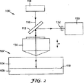
図2を参照すると、装置100が示されており、この装置100は、基板106に付着された層104のうちの選択した領域102を正確に硬化させるために使用することができる。層104は、多光子硬化性光反応組成物を含んでおり、この組成物については以下で詳細に論じることにする。本発明のプロセスを実行するにおいて、光反応組成物は、多光子吸収が発生するような条件下で光に暴露することができ、この多光子吸収によって、層のある領域において、化学的又は物理的特性の変化が生じる。そのような変化の例には、重合、架橋、及び/又は、暴露前の光反応組成物と比較した溶解度特性の変化(例えば、特定の溶媒への溶解度の減少又は増加)が挙げられる。そのような暴露は、十分な光の強度を得ることが可能な任意の既知の手段によって達成することができるが、レーザーからの集光光源が典型的には使用されている。
Referring to FIG. 2, an
装置100は、典型的にはレーザーである光源110と、ビームスプリッタ112と、集束正レンズ114とを有する第1の光学システムを含んでいる。光源110から放出された光ビーム116は、ビームスプリッタ112に入り、レンズ114によって集束され、次いで、多光子硬化性光反応材料を含んだ層104に入る。正レンズ114が、層140及び基板106に対して、z方向に沿って下向きに移動するとき、ビーム116の焦点も同様に、層104の厚さを通じて下向きに移動する。所望により、光ビーム116は、適切な波長及び十分な強度を有するように調節して、焦点において、ビームが、層104の領域102の任意の範囲内の多光子硬化性光反応材料を硬化させるようにしてもよい。層104が領域102内で硬化されるかどうかに関わらず、光ビーム116の、層104に入る部分は、層104と基板106との境界面118で反射される。境界面118から反射された後、ビーム116は、レンズ114と、ビームスプリッタ112と、検出器120とを含んだ第2の光学系に入る。
The
検出器120は、意図する用途に応じて広範囲にわたって異なっていてもよく、又、一実施形態においては、蛍光検出器を含んでおり、その蛍光検出器は、最も簡潔な事例では人間の裸眼であってもよい。光ビーム116の焦点が、層104を通じて境界面118に向かって下方に移動すると、硬化プロセスから発せられる蛍光の強度における変化を観測することができ、又、強度におけるこの変化は、ビーム116の焦点が境界面118に位置する時を判定するために使用してもよい。図2〜3を参照するが、正レンズ116がz方向に沿って下方に移動すると、ビーム116の焦点が層104に入る(図3における曲線125上の130を参照)。蛍光強度は最初のうちは増加し、次いで、ビーム116の焦点が完全に層104の内部に入ると、比較的一定な状態を維持する(図3における132を参照)。ビーム116の焦点が層104と基板106との境界面118に遭遇すると、ビーム116が完全に基板106内に焦点を合わせられる点で蛍光信号が事実上消滅するまで(図3における136を参照)、蛍光強度は急激に低下する。(図3における134を参照)
The
ビーム116の焦点が境界面118にあるとき、蛍光強度は、曲線125上の点134と136との間のどこかにある。従って、ビーム116の焦点が境界面118に存在する時を正確に判定するために検出しうる、蛍光強度の最小値又は最大値などの明確で且つ曖昧でない点は、曲線125に沿って存在しない。蛍光の整合レベルを判定するにおいて更なる複雑な要素は、層104内の多光子硬化性光反応材料を硬化させるのに使用しうる暴露のレベルが変動することである。層104内の多光子硬化性光反応材料に、更には硬化プロセスを使用して作製する硬化物体の種類に応じて、全体のレーザー出力は、又結果として全体の蛍光性は、大幅に変動しうる。このように、図3における曲線125上の点134と136との間での強度の所要低下量に対応する、z方向に沿った正レンズ114の位置の範囲も又、広範囲にわたって変動する。
When the focus of
更に、蛍光強度を使用して境界面118の位置を判定するには、正レンズ114をz方向に沿って移動させ、層104を複数回横断することも又、必要となる。これらの複数回の横断が、層104の同じ領域102内で実施された場合、その領域内の多光子硬化性光反応材料中の光開始剤が奪われ、それによって蛍光性の減少が生じる。この問題を克服するために、基板106の領域102は、新たな硬化性材料を見出すように別の領域に割り出ししてもよいが、そのような割り出し手法ではウエハー平坦度の変動がプロセスに持ち込まれ、このことは、この手法の確度に悪影響を及ぼす。
Furthermore, to determine the position of the
このように、蛍光強度の検出は有用であるが、確度及び予測性に比較的欠けていることにより、この手法の使用は、高水準の精度が要求されるときには好ましくないものとなる。しかしながら、蛍光検出は低コストで且つ簡潔であることにより、上述の手法は、境界面118の位置の比較的粗い推定値が望まれる用途に対する実用的な選択肢となっている。
Thus, although fluorescence intensity detection is useful, the relative lack of accuracy and predictability makes the use of this approach undesirable when high levels of accuracy are required. However, due to the low cost and simplicity of fluorescence detection, the above approach has become a practical option for applications where a relatively coarse estimate of the location of the
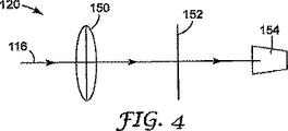
図4を参照すると、図2における装置内の検出器120の別の実施形態が示されている。図4に示す検出器120は、本明細書においては共焦点境界面位置探知システムと呼ばれるものであり、入射する光ビーム116を集束させる正レンズ150と、ピンホール152と、典型的には光電子増倍管(PMT)である検出器154とを含んでいる。共焦点境界面位置探知システム120は空間フィルターであり、単に、光ビーム116がピンホール152を通過することを、そのビームがレンズ114の焦点から生じている(図2を参照)場合に可能にするものである。従って、正レンズ114の焦点で発生した反射のみが捕捉され、PMT 154に伝えられることになる。PMT154上には、焦点が層104と基板106との境界118を交差する(図2を参照)ときにのみ信号が存在する。
Referring to FIG. 4, another embodiment of
図4の共焦点境界面位置探知システム120の空間フィルタリング効果により、正レンズ114の焦点が境界面118を交差するとき、鮮明なピーク信号が生成される。このピークは、明確に且つ明白に検出することができ、又、ピークの発生と境界面118の位置との相関性は、レーザー110の出力、第1若しくは第2の光学系における損失、又は共焦点境界面位置探知システム120自体の特性によって影響を受けることがない。加えて、共焦点境界面位置探知システム120は蛍光に依存しておらず、又、境界面118の位置の読み取りを更に確かにするために、フィルター122(図2)を任意選択により含めて、光ビーム116から蛍光波長を、そのビームが検出器120に入る前に除去してもよい。層104が基板106上に存在しない場合であっても、境界面118は依然として正確に検出することができ、従って、境界面を検出するために、層104内の光開始剤を減損させる必要がない。
Due to the spatial filtering effect of the confocal
図2及び4に示す装置は、光ビーム116を層104内に集束させるために使用されている同じ正レンズ114を利用しており、境界位置信号は、層104の領域102における硬化工程と同時に又はその硬化工程の直前に、検出器120によって受信されるので、検出器120によって取得される境界探知情報は、高度に正確なものである。図4の装置及び上述の方法を使用すると、境界面118の位置を約100nmから1μmの範囲内で判定することが可能である。境界探知情報は、層104の第1の領域内の多光子硬化性光反応材料を硬化させて第1の硬化物体を形成するときに、正レンズ114の位置を配置を維持するために使用してもよく、又、第1の領域とは異なる層104の別の領域内に別の硬化物体を形成するように正レンズ114を配置するために使用してもよい。
The apparatus shown in FIGS. 2 and 4 utilizes the same positive lens 114 that is used to focus the
図4の共焦点顕微鏡検出器に対する典型的な応答曲線160を図5に示す。PMTの出力信号における鮮明なピーク162は、層104と基板106との境界118の位置に対応している。
A
図6を参照すると、装置200の別の実施形態が示されており、この実施形態は、多光子硬化性光反応材料を含んだ層204の領域202を硬化させるために使用することができる。例えば平行アーク灯などの短コヒーレンス光源210によって放出された光ビーム216は、初めに、ビームスプリッタ212と集束正レンズ214とを含んだ第1の光学系を横断する。ビーム216は任意選択により、層204の領域202内の多光子硬化性光反応材料を硬化させるか、又はその多光子硬化性光反応材料の硬化を引き起こす。次いで、ビーム216の一部分が、層204と基板206との境界面218から反射され、正レンズ214と、ビームスプリッタ212と、ミラー215とを含んだ第2の光学系に入る。ミラー215から反射された光は、再びビームスプリッタ212を通過し、PMTなどの検出器220に入る。正レンズ214の焦点が、境界面218に位置しているとき、第1及び第2の光学系を横断する光波の間での強めあう干渉により、強い信号が検出器220において生じる。正レンズ214の焦点が、境界面218に位置していないとき、第1及び第2の光学系を横断する光波の間での弱めあう干渉により、相対的により弱い信号が検出器220において生じる。
Referring to FIG. 6, another embodiment of the
図7に示す更に別の実施形態において、分割検出器焦点測定システム及び装置300が示されており、このシステム及び装置300は、多光子硬化性光反応材料を含んだ層304の領域302を硬化させるために使用することができる。平行源310から放出された光ビーム316は、ビームスプリッタ312と、焦点調整対物レンズ314とを含んだ第1の光学系を横断する。ビーム316は任意選択により、層304の領域302内の多光子硬化性光反応材料を硬化させるか、又はその多光子硬化性光反応材料の硬化を引き起こす。次いで、ビーム316の一部分が、層304と基板306との境界面318から反射され、対物レンズ314と、ビームスプリッタ312と、ビームの半分を遮断する不透明スクリーン321と、焦点調整用レンズ319と、分割検出器320とを含んだ第2の光学系に入る。ビームが、層304と基板306との境界面318に焦点を定められると、次いで、結果として生じるビームが、分割検出器320の中心で探知される。分割検出器の2つの側の間での信号の差異はゼロとなる。ビームが、層304と基板306との境界面318の上方又は下方に焦点を定められると、結果として生じるビームは、分割検出器の一方の側又は他方の側において、更に焦点を定められる。分割検出器の2つの側の間での信号の差異はゼロとはならず、その大きさは焦点ずれの量を示し、差異信号の符号は焦点ずれの方向を示す。
In yet another embodiment shown in FIG. 7, a split detector focus measurement system and
図8を参照すると、多光子硬化性光反応材料を含んだ層404の領域402を硬化させるために使用することができる装置400が示されている。層404は、基板406に塗布されており、基板406は調整可能なプラットフォーム又はステージ405上に置かれている。z方向に沿ったステージ405の高さ、並びに層404のx−y平面の上方又は下方への傾きは、手動で、又は制御ライン472を通じてデジタルコンピュータ470によって調整することが可能である。集光光源410から放出された光ビーム416はまず、ビームスプリッタ412と、焦点調整用正レンズ414とを含んだ第1の光学系を横断する。z方向に沿った焦点調整用正レンズ414の高さも又、手動で、又は制御ライン474を通じてデジタルコンピュータ470によって調整することが可能である。正レンズ414を去った後、光ビーム416は層404に入り、任意選択により、層404の領域402内の多光子硬化性光反応材料を硬化させるか、又はその多光子硬化性光反応材料の硬化を引き起こし、又、光ビーム416の一部分は、境界面418において基板406から反射される。光ビーム416は次いで、正レンズ414と検出器420とを含んだ第2の光学系に入る。検出器420は、図2及び4に示すような共焦点境界面位置探知システム120であっても、図6に示すような干渉検出システムであっても、図7に示すような分割検出器であってもよい。
Referring to FIG. 8, there is shown an
次いで、検出器420の出力が、ライン471伝いにデジタルコンピュータ470に与えられる。図9を更に参照すると、工程500で初期化した後、コンピュータ470は工程502において、正レンズ414及び調整可能なステージ405からの配置データ、並びに検出器420からのデータを受信する。工程504において、コンピュータ470は、検出器からの信号を、境界面418に対するz方向沿いの正レンズ414の高さ、並びにステージ405の傾斜角と関連付ける。例えば、図9に示すように、検出器470が共焦点境界面位置探知システムでありPMTを有している場合、PMTの最大出力は、正レンズ414の焦点が層404と基板406との境界面418に存在する、z方向に沿った正レンズ414の位置と関連付けることができる。工程506において、配置データ及び検出器データがコンピュータ470に入力され、工程508において、コンピュータが検出器データを評価して、PMT信号が最大値にあるかどうかを判定する。「はい」の場合、z方向に沿った正レンズ414の配置は変更されない。「いいえ」の場合、工程510において、コンピュータが、z軸に沿った正レンズ414の高さを、PMT信号が再び最大値となるまで調節する。
The output of
この連続的なフィードバックシステムを使用すると、上述の方法及び装置は、境界面418を多数の方式で正確に見出すために使用することができる。例えば、静的な方法において、検出器470は、層404/基板406の境界面を、基板406の表面上の異なる個所で、典型的には少なくとも3個所で標本抽出するために、光学プローブとして使用される。境界面418の位置に対するz軸に沿った正レンズ411の配置が、基板406上の全ての標本抽出位置に対して約±0.5μm以内でない場合、コンピュータ470は、正レンズ414及び/又はステージ405のいずれかを調節するのに必要な計算を実施する。基板406が、正レンズ414下部のx軸に沿った動作平面に対して十分に水平となると、光ビーム416を使用して、層404の領域402を硬化させることができる。この方法は、x−y平面に対する基板の傾斜角しか補正することができないため、十分に平坦な基板上でしか使用することができない。
Using this continuous feedback system, the methods and apparatus described above can be used to accurately find the
又、正レンズ414が移動し、層404内の多光子硬化性光反応材料が硬化して物体を形成するとき、境界面418の位置についての連続的なフィードバックを与えるために、動的な方法を使用してもよい。この方法は、層404の第1の領域から第2の領域へ、又以下同様に硬化が進行するとき、z軸に沿った正レンズ414の配置が連続的に補正されるので、基板406の表面内のいかなる非平坦性をも補正することができる。又、この連続的な動的フィードバックでは、球面及び非球面など、名目上平坦でない表面上に構造を構築することも可能となる。
A dynamic method is also used to provide continuous feedback on the location of the
本明細書で説明するプロセスにおいて有用な多光子硬化性光反応組成物については、参照によってその全てが本願に援用される、3M代理人整理番号60893US002と同時係属であり且つ同時出願された出願において詳細に論じられている。 For multiphoton curable photoreactive compositions useful in the processes described herein, in the co-pending and co-filed application with 3M Attorney Docket No. 60893 US002, all of which is incorporated herein by reference. It is discussed in detail.
塗布層内の多光子硬化性光反応組成物は、酸又はラジカル開始による化学反応を受けることが可能な少なくとも1つの反応種、並びに多光子開始剤系を含んでいる。適当な波長及び十分な強度の光で層を像様に暴露することにより、多光子開始剤系内で二光子吸収が生じ、この二光子吸収により、反応種において、光に暴露された層の領域内に、酸又はラジカル開始による化学反応が誘起される。この化学反応は光に暴露された層の領域内の、化学的又は物理的特性に検出可能な変化を生じる。検出可能な変化の例には、例えば、架橋、重合、又は、暴露領域における溶解度特性の変化が挙げられる。これらの検出可能な変化のうちのいずれかが発生することを、本明細書においては硬化と呼び、又この硬化は、硬化物体が形成されるまで継続する。硬化工程は、層が塗布された基板との境界面付近を含めて、多光子光反応組成物を含んだ層内のいかなる範囲においても起こりうる。硬化工程に続いて、層の非硬化部分を除去して硬化物体を取得することによって、又は硬化物体自体を層から取り出すことによって、層を任意選択により成長させてもよい。 The multiphoton curable photoreactive composition in the coating layer includes at least one reactive species capable of undergoing a chemical reaction by acid or radical initiation, as well as a multiphoton initiator system. Imagewise exposure of the layer with the appropriate wavelength and sufficient intensity of light results in two-photon absorption within the multiphoton initiator system, and this two-photon absorption causes the reactive species of the layer exposed to light. In the region, a chemical reaction is induced by acid or radical initiation. This chemical reaction produces a detectable change in chemical or physical properties within the area of the layer exposed to light. Examples of detectable changes include, for example, cross-linking, polymerization, or changes in solubility characteristics in the exposed area. The occurrence of any of these detectable changes is referred to herein as curing, and this curing continues until a cured object is formed. The curing step can occur anywhere within the layer containing the multiphoton photoreactive composition, including near the interface with the substrate on which the layer is applied. Following the curing step, the layer may optionally be grown by removing the uncured portion of the layer to obtain a cured object, or by removing the cured object itself from the layer.
反応種
光反応組成物内で使用するのに好適な反応種には、硬化性の化学種と非硬化性の化学種の双方が挙げられる。硬化性の化学種が一般に好ましく、又硬化性の化学種には、例えば、付加重合性モノマー及びオリゴマーと付加架橋性ポリマー(例えばアクリレート、メタクリレート、及びスチレンなどの特定のビニル化合物を含む、ラジカル重合性又は架橋性のエチレン不飽和性の化学種)、更には、カチオン重合性モノマー及びオリゴマーとカチオン架橋性ポリマー(この化学種は最も一般的には酸開始されており、又この化学種には、例えばエポキシ、ビニルエーテル、シアネートエステルなどが挙げられる)、その他同種のもの、並びにそれらの混合物が挙げられる。
Reactive species Suitable reactive species for use in the photoreactive composition include both curable and non-curable species. Curable species are generally preferred, and curable species include, for example, radical polymerization, including addition polymerizable monomers and oligomers and addition crosslinkable polymers (eg, specific vinyl compounds such as acrylates, methacrylates, and styrene). , Or cationically polymerizable monomers and oligomers, and cationically crosslinkable polymers (this species is most commonly acid-initiated, and For example, epoxy, vinyl ether, cyanate ester, and the like), and the like, and mixtures thereof.
好適なエチレン不飽和性の化学種については、例えば、パラツォット(Palazzotto)らによって米国特許第5,545,676号において第1欄65行から第2欄26行で述べられており、モノアクリレート、ジアクリレート、ポリアクリレート及びメタクリレート(例えば、メチルアクリレート、メチルメタクリレート、エチルアクリレート、イソプロピルメタクリレート、n−ヘキシルアクリレート、ステアリルアクリレート、アリルアクリレート、グリセロールジアクリレート、グリセロールトリアクリレート、エチレングリコールジアクリレート、ジエチレングリコールジアクリレート、トリエチレングリコールジメタクリレート、1,3−プロパンジオールジアクリレート、1,3−プロパンジオールジメタクリレート、トリメチロールトリアクリレート、1,2,4−ブタントリオールトリメタクリレート、1,4−シクロヘキサンジオールジアクリレート、ペンタエリトリトールトリアクリレート、ペンタエリトリトールテトラアクリレート、ペンタエリトリトールテトラメタクリレート、ソルビトールヘキサアクリレート、ビス[1−(2−アクリルオキシ)]−p−エトキシフェニルジメチルメタン、ビス[1−(3−アクリルオキシ−2−ヒドロキシ)]−p−プロポキシフェニルジメチルメタン、トリスヒドロキシエチル−イソシアヌレートトリメタクリレート、分子量が約200〜500のポリエチレングリコールのビスアクリレート及びビスメタクリレート、米国特許第4,652,274号のものなどのアクリル化モノマーと米国特許第4,642,126号のものなどのアクリル化オリゴマーとの共重合性混合物)、不飽和酸アミド(例えば、メチレンビスアクリレート、メチレンビスメタクリルアミド、1,6−ヘキサメチレンビスアクリルアミド、ジエチレントリアミン、トリスアクリルアミド及びベータメタクリルアミノエチルメタクリレート)、ビニル化合物(例えば、スチレン、ジアリルフタレート、ジビニルスクシネート、ジビニルアジペート、及びジビニルフタレート)、その他同種のもの、並びにそれらの混合物が挙げられる。好適な反応性ポリマーには、例えば1から約50のアクリル(メタクリート)基をポリマー鎖ごとに有する、ペンダントアクリレート(メタクリレート)基を有するポリマーが挙げられる。そのようなポリマーの例には、サートマー(Sartomer)社から入手可能なSarbox(商標)樹脂(例えば、Sarbox(商標)400、401、402、404、及び405)などの芳香族酸(メタクリレート)アクリレート半エステル樹脂が挙げられる。フリーラジカル化学によって硬化可能な他の有用な反応性ポリマーには、ヒドロカルビル主鎖と、米国特許第5,235,015号(アリ(Ali)ら)において記載されているものなど、ラジカル重合可能な官能性を付与されたペンダントペプチド基とを有するポリマーが挙げられる。2つ以上のモノマー、オリゴマー、及び/又は反応性高分子の混合物を、所望に応じて使用することができる。好ましいエチレン不飽和性の化学種には、アクリレート、芳香族酸(メタクリレート)アクリレート半エステル樹脂、及び、ヒドロカルビル主鎖と、ラジカル重合化可能な官能性を付与されたペンダントペプチド基とを有するポリマーが挙げられる。
Suitable ethylenically unsaturated species are described, for example, by Palazzotto et al. In US Pat. No. 5,545,676, column 1, line 65 to column 2,
好適なカチオン反応性の化学種については、例えばオクスマン(Oxman)らによって米国特許第5,998,495号及び6,025,406号において記載されており、又この化学種はエポキシ樹脂を含んでいる。そのような材料は、概してエポキシドと呼ばれるものであり、低分子量のエポキシ化合物と高分子量型のエポキシドとがあり、脂肪族、脂環式、芳香族、又は複素環式となりうる。これらの材料は一般に、平均して、分子1個あたり少なくとも1個(好ましくは少なくとも約1.5個、より好ましくは少なくとも約2個)の重合可能なエポキシ基を有している。ポリマーエポキシドには、末端エポキシ基を有する線状ポリマー(例えば、ポリオキシアルキレングリコールのジグリシジルエーテル)、骨格オキシラン単位を有するポリマー(例えば、ポリブタジエンポリエポキシド)、ペンダントエポキシ基を有するポリマー(例えば、グリシジルメタクリレートポリマー又はコポリマー)が挙げられる。エポキシドは、純粋化合物とすることができ、又、分子1個当たり1個、2個、又はそれ以上のエポキシ基を含有する化合物の混合物とすることができる。これらのエポキシ含有材料は、主鎖及び置換基の種類において、非常に多様となりうる。例えば、主鎖は任意の種類とすることができ、又、その主鎖上の置換基は、カチオン硬化を室温で実質的に妨げることのない任意の基とすることができる。許容しうる置換基の実例には、ハロゲン、エステル基、エーテル、スルホネート基、シロキサン基、ニトロ基、リン酸基、及び同種のものが挙げられる。エポキシ含有材料の分子量は、約58から約100,000以上まで様々となりうる。 Suitable cationic reactive species are described, for example, by Oxman et al. In US Pat. Nos. 5,998,495 and 6,025,406, and these species include epoxy resins. Yes. Such materials are generally referred to as epoxides, including low molecular weight epoxy compounds and high molecular weight epoxides, which can be aliphatic, alicyclic, aromatic, or heterocyclic. These materials generally have, on average, at least 1 (preferably at least about 1.5, more preferably at least about 2) polymerizable epoxy groups per molecule. Polymer epoxides include linear polymers having terminal epoxy groups (eg, diglycidyl ether of polyoxyalkylene glycol), polymers having backbone oxirane units (eg, polybutadiene polyepoxide), polymers having pendant epoxy groups (eg, glycidyl methacrylate). Polymer or copolymer). The epoxide can be a pure compound or a mixture of compounds containing one, two, or more epoxy groups per molecule. These epoxy-containing materials can vary greatly in the type of backbone and substituents. For example, the main chain can be of any type and the substituents on the main chain can be any group that does not substantially interfere with cationic curing at room temperature. Illustrative examples of acceptable substituents include halogens, ester groups, ethers, sulfonate groups, siloxane groups, nitro groups, phosphate groups, and the like. The molecular weight of the epoxy-containing material can vary from about 58 to about 100,000 or more.
有用な他のエポキシ含有材料には、以下の式のグリシジルエーテルモノマーが挙げられる。 Other useful epoxy-containing materials include glycidyl ether monomers of the following formula:

上式で、R’はアルキル又はアリルであり、nは1から8の整数である。その実例は、多価フェノールをエピクロロヒドリンなどの過剰なクロロヒドリンと反応させることによって得られる、多価フェノールのグリシジルエーテル(例えば、2,2−ビス−(2,3−エポキシプロポキシフェノール)−プロパンのグリシジルエーテル)である。この種のエポキシドの更なる例が、米国特許第3,018,262号に、又、「エポキシ樹脂ハンドブック(Handbook of Epoxy Resins)」、リー及びネビル(Lee and Neville)著、McGraw−Hill Book Co.,New York(1967)に記載されている。 In the above formula, R 'is alkyl or allyl, and n is an integer of 1 to 8. Illustrative examples are glycidyl ethers of polyhydric phenols (eg, 2,2-bis- (2,3-epoxypropoxyphenol)-, obtained by reacting polyhydric phenols with excess chlorohydrin such as epichlorohydrin. Glycidyl ether of propane). Further examples of this type of epoxide are given in US Pat. No. 3,018,262, also “Handbook of Epoxy Resins”, by Lee and Neville, McGraw-Hill Book Co . , New York (1967).
多数の商業的に入手可能なエポキシモノマー又は樹脂を使用することができる。容易に入手可能なエポキシドには、オクタデシレンオキシド、エピクロロヒドリン、スチレンオキシド、ビニルシクロヘキセンオキシド、グリコール、グリシジルメタクリレート、ビスフェノールAのジグリシジルエーテル(例えば、オハイオ州コロンバス(Columbus)のヘキシオンスペシャルティケミカルズ社(Hexion Specialty Chemicals, Inc.)から「EPON 815C」、「EPON 813」、「EPON 828」、「EPON 1004F」、及び「EPON 1001F」の商標表記で入手可能なもの)、及びビスフェノールFのジグリシジルエーテル(例えば、スイス国バーゼル(Basel)のチバスペシャルティケミカルズホールディング社(Ciba Specialty Chemicals Holding Company)から「ARALDITE GY281」の商標表記で、又、オハイオ州コロンバス(Columbus)のヘキシオンスペシャルティケミカルズ社(Hexion Specialty Chemicals, Inc.)から「EPON 862」の商標表記で入手可能なもの)が挙げられるが、これらに限定するものではない。他の芳香族エポキシ樹脂には、マサチューセッツ州ニュートン(Newton)のマイクロケム社(MicroChem Corp.)から入手可能なSU−8樹脂が挙げられる。 A number of commercially available epoxy monomers or resins can be used. Easily available epoxides include octadecylene oxide, epichlorohydrin, styrene oxide, vinylcyclohexene oxide, glycol, glycidyl methacrylate, diglycidyl ether of bisphenol A (eg, hexion specialty from Columbus, Ohio). Of "EPON 815C", "EPON 813", "EPON 828", "EPON 1004F" and "EPON 1001F") from Hexion Specialty Chemicals, Inc., and bisphenol F Diglycidyl ethers (eg CARD Specialty Chemicals Holding Company, Basel, Switzerland) under the trademark designation “ALALDITE GY281” Such as, but not limited to, “EPON 862” trademark designation from Hexion Specialty Chemicals, Inc. of Columbus, Ohio. Other aromatic epoxy resins include SU-8 resin available from MicroChem Corp. of Newton, Massachusetts.
他の例示的なエポキシモノマーには、ビニルシクロヘキセンジオキシド(ペンシルバニア州ウェストチェスター(West Chester)のSPIサプライズ社(SPI Supplies)から入手可能)、4−ビニル−1−シクロヘキセンジオキシドジエポキシド(ウィスコンシン州ミルウォーキー(Milwaukee)のアルドリッチケミカル社(Aldrich Chemical Co.)から入手可能)、3,4−エポキシシクロヘキシルメチル−3,4−エポキシシクロヘキセン(例えば、ミシガン州ミッドランド(Midland)のダウケミカル社(Dow Chemical Co.)から商標表記「CYRACURE UVRー6110」として入手可能なもの)、3,4−エポキシ−6−メチルシクロヘキシルメチル−3,4−エポキシ−6−メチル−シクロヘキサンカーボネート、2−(3,4−エポキシシクロヘキシル−5,5−スピロ−3,4−エポキシ)シクロヘキサン−メタジオキサン、ビス(3,4−エポキシシクロヘキシルメチル)アジペート(例えば、ダウケミカル社(Dow Chemical Co.)から商標表記「CYRACURE UVR−6128」として入手可能なもの)、ビス(3,4−エポキシ−6−メチルシクロヘキシルメチル)アジペート、3,4−エポキシ−6−メチルシクロヘキサンカルボキシレート、及びジペンテンジオキシドが挙げられる。 Other exemplary epoxy monomers include vinylcyclohexene dioxide (available from SPI Supplies, West Chester, PA), 4-vinyl-1-cyclohexene dioxide diepoxide (Wisconsin). Available from Aldrich Chemical Co., Milwaukee), 3,4-epoxycyclohexylmethyl-3,4-epoxycyclohexene (eg, Dow Chemical Co., Midland, Michigan). Available under the trade designation “CYRACURE UVR-6110”), 3,4-epoxy-6-methylcyclohexylmethyl-3,4-epoxy-6-methyl-cyclohexane carbonate, 2- (3,4- Epoxy cyclohexyl −5,5-spiro-3,4-epoxy) cyclohexane-metadioxane, bis (3,4-epoxycyclohexylmethyl) adipate (eg, “CYRACURE UVR-6128” from Dow Chemical Co.) Bis (3,4-epoxy-6-methylcyclohexylmethyl) adipate, 3,4-epoxy-6-methylcyclohexanecarboxylate, and dipentene dioxide.
更に他の例示的なエポキシ樹脂として、エポキシ化ポリブタジエン(例えば、ペンシルバニア州エクストン(Exton)のサートマー社(Sartomer Co., Inc.)から商標表記「POLY BD605E」として入手化なもの)、エポキシシラン(例えば、ウィスコンシン州ミルウォーキー(Milwaukee)のアルドリッチケミカル社(Aldrich Chemical Co.)から商業的に入手可能な3,4−エポキシシクロヘキシルエチルトリメトキシシラン及び3−グリシドキシプロピルトリメトキシシラン)、難燃性エポキシモノマー(例えば、ミシガン州ミッドランド(Midland)のダウケミカル社(Dow Chemical Co.)から入手可能な、臭素化ビスフェノール型エポキシモノマーであって、商標表記「DER−542」として入手可能なもの)、1,4−ブタンジオールジグリシジルエーテル(例えば、チバスペシャルティケミカルズ社(Ciba Specialty Chemicals)から商標表記「ARALDITE RD−2」として入手可能なもの)、臭素化ビスフェノールA−エピクロロヒドリン系エポキシモノマー(例えば、ヘキシオンスペシャルティケミカルズ社(Hexion Specialty Chemicals, Inc.)から商標表記「EPONEX 1510」として入手可能なもの)、フェノール−ホルムアルデヒドノボラックのポリグリシジルエーテル(例えば、ダウケミカル社(Dow Chemical Co.)から商標表記「DEN−431」及び「DEN−438」として入手可能なもの)、並びに、アトフィナケミカルズ社(Atofina Chemicals)(ペンシルバニア州フィラデルフィア(Philadelphia))から商標表記「VIKOLOX」及び「VIKOFLEX」として入手可能な、エポキシ化した亜麻仁油及び大豆油などのエポキシ化した植物油が挙げられる。 Still other exemplary epoxy resins include epoxidized polybutadiene (eg, available under the trade designation “POLY BD605E” from Sartomer Co., Inc., Exton, Pa.), Epoxy silane ( For example, 3,4-epoxycyclohexylethyltrimethoxysilane and 3-glycidoxypropyltrimethoxysilane, commercially available from Aldrich Chemical Co., Milwaukee, Wis., Flame retardant Epoxy monomers (e.g., brominated bisphenol type epoxy monomers available from Dow Chemical Co., Midland, Michigan, available under the trade designation "DER-542"), 1,4-butanediol diglycidyl -Tel (for example, available from Ciba Specialty Chemicals under the trade designation “ALALDITE RD-2”), brominated bisphenol A-epichlorohydrin epoxy monomer (for example, Hexion Specialty Chemicals ( Available from Hexion Specialty Chemicals, Inc.) under the trade designation "EPONEX 1510"), polyglycidyl ethers of phenol-formaldehyde novolac (e.g. the trade designation "DEN-431" from Dow Chemical Co.) Available as “DEN-438”) and the trademark designations “VIKOLOX” and “VIKOFLEX” from Atofina Chemicals (Philadelphia, Pa.), And epoxidized vegetable oils such as epoxidized linseed oil and soybean oil.
更なる好適なエポキシ樹脂には、ヘキシオンスペシャルティケミカルズ社(Hexion Specialty Chemicals, Inc.)(オハイオ州コロンバス(Columbus))から商標表記「HELOXY」として商業的に入手可能なアルキルグリシジルエーテルが挙げられる。例示的なモノマーには、「HELOXY MODFIER 7」(C8〜C10アルキルグリシジルエーテル)、「HELOXY MODFIER 8」(C12〜C14アルキルグリシジルエーテル)、「HELOXY MODFIER 61」(ブチルグリシジルエーテル)、「HELOXY MODFIER 62」(クレジルグリシジルエーテル)、「HELOXY MODFIER 65」(p−t−ブチルフェニルグリシジルエーテル)、「HELOXY MODFIER 67」(1,4−ブタンジオールのジグリシジルエーテル)、「HELOXY 68」(ネオペンチルグリコールのジグリシジルエーテル)、「HELOXY MODFIER 107」(シクロヘキサンジメタノールのジグリシジルエーテル)、「HELOXY MODFIER 44」(トリメチロールエタントリグリシジルエーテル)、「HELOXY MODFIER 48」(トリメチロールプロパントリグリシジルエーテル)、「HELOXY MODFIER 84」(脂肪族ポリオールのポリグリシジルエーテル)、及び、「HELOXY MODFIER 32」(ポリグリコールジエポキシド)が挙げられる。
Further suitable epoxy resins include alkyl glycidyl ethers commercially available from Hexion Specialty Chemicals, Inc. (Columbus, Ohio) under the trademark designation “HELOXY”. Exemplary monomers include “HELOXY MODFIER 7” (C 8 -C 10 alkyl glycidyl ether), “HELOXY MODFIER 8” (C 12 -C 14 alkyl glycidyl ether), “HELOXY MODFIER 61” (butyl glycidyl ether), “HELOXY MODIFER 62” (cresyl glycidyl ether), “HELLOXY MODFIER 65” (pt-butylphenylglycidyl ether), “HELLOXY MODFIER 67” (diglycidyl ether of 1,4-butanediol), “HELOXY 68” (Diglycidyl ether of neopentyl glycol), “HELOXY MODIFER 107” (diglycidyl ether of cyclohexanedimethanol), “HELOXY MODF IER 44 "(trimethylol ethane triglycidyl ether)," HELLOXY MODFIER 48 "(trimethylol propane triglycidyl ether)," HELLOXY MODFIER 84 "(polyglycidyl ether of aliphatic polyols), and"
他の有用なエポキシ樹脂は、グリシドールのアクリル酸エーテル(グリシジルアクリレート及びグリシジルメタクリレートなど)と1つ以上の共重合性ビニル化合物とのコポリマーを含んでいる。そのようなコポリマーの例が、1:1のスチレン−グリシジルメタクリレート及び1:1のメチルメタクリレート−グリシジルアクリレートである。他の有用なエポキシ樹脂が周知であり、エピクロルヒドリン、アルキレンオキシド(例えばプロピレンオキシド)、スチレンオキシド、アルケニルオキシド(例えばブタジエンオキシド)、及びグリシジルエステル(例えばエチルグリシデート)のようなエポキシドを含有している。 Other useful epoxy resins include copolymers of glycidol acrylate ethers (such as glycidyl acrylate and glycidyl methacrylate) with one or more copolymerizable vinyl compounds. Examples of such copolymers are 1: 1 styrene-glycidyl methacrylate and 1: 1 methyl methacrylate-glycidyl acrylate. Other useful epoxy resins are well known and contain epoxides such as epichlorohydrin, alkylene oxides (eg propylene oxide), styrene oxide, alkenyl oxides (eg butadiene oxide), and glycidyl esters (eg ethyl glycidate). .
有用なエポキシ官能性ポリマーには、ゼネラルエレクトリック社(General Electric Company)から商業的に入手可能な、米国特許第4,279,717号(エクバーグ(Eckberg)ら)に記載されているものなどのエポキシ官能性シリコーンが挙げられる。これらは、ケイ素原子の1モル%〜20モル%がエポキシアルキル基(好ましくは、米国特許第5,753,346号(レイア(Leir)ら)に記載されているように、エポキシシクロヘキシルエチル)で置換されたポリジメチルシロキサンである。 Useful epoxy functional polymers include epoxies such as those described in US Pat. No. 4,279,717 (Eckberg et al.), Commercially available from General Electric Company. Examples include functional silicones. These are those in which 1 mol% to 20 mol% of silicon atoms are epoxyalkyl groups (preferably epoxycyclohexylethyl as described in US Pat. No. 5,753,346 (Leir et al.)). Substituted polydimethylsiloxane.
又、種々のエポキシ含有材料の配合物を利用することもできる。そのような配合物は、エポキシ含有化合物(低分子量(200未満)、中分子量(約200から1000)、及び高分子量(約1000超)など)の2つ以上の重量平均分子量分布を備えていてもよい。その代わりに又はそれに加えて、エポキシ樹脂は、異なる化学的性質(脂肪族及び芳香族など)又は官能性(極性及び無極性など)を有するエポキシ含有材料の配合物を含むことができる。他のカチオン反応性ポリマー(ビニルエーテル及び同種のものなど)を、所望に応じて更に混和することができる。 It is also possible to use blends of various epoxy-containing materials. Such formulations have two or more weight average molecular weight distributions of epoxy-containing compounds (such as low molecular weight (less than 200), medium molecular weight (about 200 to 1000), and high molecular weight (greater than about 1000)). Also good. Alternatively or additionally, the epoxy resin can include a blend of epoxy-containing materials having different chemical properties (such as aliphatic and aromatic) or functionalities (such as polar and nonpolar). Other cationic reactive polymers (such as vinyl ethers and the like) can be further blended if desired.
好ましいエポキシには、芳香族グリシジルエポキシ(例えば、ヘキシオンスペシャルティケミカルズ社(Hexion Specialty Chemicals, Inc.)から入手可能なEPON樹脂、及びマサチューセッツ州ニュートン(Newton)のマイクロケム社(MicroChem Corp.)から入手可能なSU−8樹脂)、その他同種のもの、及びそれらの混合物が挙げられる。より好ましいのは、SU−8樹脂及びこれらの混合物である。 Preferred epoxies include aromatic glycidyl epoxies (eg, EPON resin available from Hexion Specialty Chemicals, Inc., and MicroChem Corp., Newton, Mass.). Possible SU-8 resins), the like, and mixtures thereof. More preferred are SU-8 resins and mixtures thereof.
又、好適なカチオン反応性の化学種には、ビニルエーテルモノマー、オリゴマー、及び反応性ポリマー(例えば、メチルビニルエーテル、エチルビニルエーテル、t−ブチルビニルエーテル、イソブチルビニルエーテル、トリエチレングリコールジビニルエーテル(ニュージャージー州ウェイン(Wayne)のインターナショナルスペシャルティプロダクツ社(International Specialty Products)から入手可能なRAPI−CURE DVE−3)、トリメチロールプロパントリビニルエーテル、及びノースカロライナ州グリーンズボロ(Greensboro)のモーフレックス社(Morflex, Inc.)によるVECTOMERジビニルエーテル樹脂(例えば、VECTOMER 1312、VECTOMER 4010、VECTOMER 4051、及びVECTOMER 4060、並びに他の製造業者から入手可能なそれらの等価物)、並びにそれらの混合物が挙げられる。又、1つ以上のビニルエーテル及び/又は1つ以上のエポキシ樹脂の(任意の比率における)配合物を利用することもできる。又、ポリヒドロキシ官能性材料(例えば米国特許第5,856,373号(カイサキ(Kaisaki)ら)に記載されているものなど)を、エポキシ−及び/又はビニルエーテル官能性材料と共に利用することもできる。 Suitable cationic reactive species also include vinyl ether monomers, oligomers, and reactive polymers (eg, methyl vinyl ether, ethyl vinyl ether, t-butyl vinyl ether, isobutyl vinyl ether, triethylene glycol divinyl ether (Wayne, NJ) RAPI-CURE DVE-3), trimethylolpropane trivinyl ether, available from International Specialty Products, and VECTOMER dice from Morflex, Inc., Greensboro, NC Vinyl ether resins (eg, VECTOMER 1312, VECTOMER 4010, VECTOMER 4051, and VECTOMER 4 060, and their equivalents available from other manufacturers), and mixtures thereof, and blends (in any ratio) of one or more vinyl ethers and / or one or more epoxy resins. Alternatively, polyhydroxy functional materials (such as those described in US Pat. No. 5,856,373 (Kaisaki et al.)) Can be used with epoxy- and / or vinyl ether functionalities. It can also be used with materials.
非硬化性の化学種には、例えば、酸又はラジカル誘起反応の際に溶解度が増加しうる反応性ポリマーが挙げられる。そのような反応性ポリマーには、例えば、光生成した酸によって可溶性の酸基へと変換されうるエステル基を持つ非水溶性ポリマー(例えば、ポリ(4−t−ブトキシカルボニルオキシスチレン))が挙げられる。又、非硬化性の化学種には、R.D.アレン(R. D. Allen)、G.M.ワルラフ(G. M. Wallraff)、W.D.ヒンスバーグ(W. D. Hinsberg)、及びL.L.シンプソン(L. L. Simpson)によって、「化学増幅フォトレジスト用途のための高性能アクリルポリマー(High Performance Acrylic Polymers for Chemically Amplified Photoresist Applications)」、J.Vac.Sci.Technol.B,9,3357(1991)に記載された化学増幅フォトレジストが挙げられる。化学増幅フォトレジストの構想は、特に0.5サブミクロン(又は更に0.2サブミクロン)の機構を伴うマイクロチップ製造に、現在では広く用いられている。そのようなフォトレジスト系においては、触媒性の化学種(典型的には水素イオン)を照射によって生成することができ、この照射によって化学反応の電子なだれが誘発される。この電子なだれは、より多くの水素イオン又は他の酸性の化学種を生成する反応を水素イオンが開始し、それによって反応速度が増幅されるときに発生する。典型的な、酸を触媒とする化学増幅フォトレジスト系の例には、脱保護(例えば、米国特許第4,491,628号に記載されているt−ブトキシカルボニルオキシスチレンのレジスト、テトラヒドロピラン(THP)メタクリレート系の物質、米国特許第3,779,778号に記載されているものなどのTHPフェノール物質、R.Dアレン(R. D Allen)らによってProc.SPIE 2438,474(1995)に記載されているものなどのt−ブチルメタクリレート系の物質、その他同種のもの)、解重合(例えば、ポリフタルアルデヒド系の物質)、及び転位(例えば、ピナコール転位に基づく物質)が挙げられる。 Non-curable chemical species include, for example, reactive polymers that can increase solubility during acid or radical induced reactions. Such reactive polymers include, for example, water insoluble polymers (eg, poly (4-tert-butoxycarbonyloxystyrene)) having ester groups that can be converted to soluble acid groups by photogenerated acid. It is done. Non-curable chemical species include R.I. D. R. D. Allen, G. M.M. Warm (G. M. Wallraff), W. D. H. D. Hinsberg, and L. L. L. L. Simpson, “High Performance Acrylic Polymers for Chemically Amplified Photoresist Applications”, J. Am. Vac. Sci. Technol. B, 9, 3357 (1991). The concept of chemically amplified photoresist is now widely used, especially for microchip manufacturing with 0.5 submicron (or even 0.2 submicron) features. In such photoresist systems, catalytic species (typically hydrogen ions) can be generated by irradiation, which induces an avalanche of chemical reaction. This avalanche occurs when a hydrogen ion initiates a reaction that produces more hydrogen ions or other acidic species, thereby amplifying the reaction rate. Examples of typical acid-catalyzed chemically amplified photoresist systems include deprotection (eg, the t-butoxycarbonyloxystyrene resist described in US Pat. No. 4,491,628, tetrahydropyran ( THP) methacrylate based materials, THP phenolic materials such as those described in US Pat. No. 3,779,778, R. D Allen et al., Proc. SPIE 2438, 474 (1995). T-butyl methacrylate based materials such as those described, and the like), depolymerization (eg, polyphthalaldehyde based materials), and rearrangements (eg, materials based on pinacol rearrangement).
所望により、異なる種類の反応種の混合物を光反応性組成物中に利用してもよい。例えば、ラジカル反応種とカチオン反応種の混合物も又有用である。 If desired, a mixture of different types of reactive species may be utilized in the photoreactive composition. For example, mixtures of radical and cation reactive species are also useful.
光開始剤系
この光開始剤系は多光子光開始剤系であるが、これは、そのような系を使用することにより、光の集束ビームの焦点領域に重合作用を制限又は限定することが可能となるからである。そのような系は好ましくは、少なくとも1つの多光子光増感剤と、少なくとも1つの光開始剤(又は電子受容体)と、任意選択による少なくとも1つの電子供与体とを含む二成分又は三成分系であるそのような多成分系は感度の向上をもたらすことができ、光反応をより短い期間で成し遂げることが可能であり、それによって、サンプル及び/又は露光系の1つ以上の成分の動きに起因する問題が生じる可能性が減じられる。
Photoinitiator system This photoinitiator system is a multi-photon photoinitiator system, which can limit or limit the polymerization action to the focal region of the focused beam of light by using such a system. This is because it becomes possible. Such a system is preferably a two or three component comprising at least one multiphoton photosensitizer, at least one photoinitiator (or electron acceptor), and optionally at least one electron donor. Such a multi-component system, which is a system, can provide an improvement in sensitivity and can achieve a photoreaction in a shorter period of time, whereby movement of one or more components of the sample and / or exposure system This reduces the possibility of problems caused by.
好ましくは、多光子光開始剤系は、光化学的に効果的な量の、(a)少なくとも2個の光子を同時に吸収することが可能であり、任意選択であるが好ましくはフルオロセインよりも大きな二光子吸収断面を有する、少なくとも1つの多光子光増感剤と、(b)多光子光増感剤とは異なるものであり、電子励起状態の光増感剤に電子を供与することが可能な、任意選択による少なくとも1つの電子供与体化合物と、(c)電子励起状態の光増感剤から電子を受容することによって光増感することが可能であり、結果として、少なくとも1つのラジカル及び/又は酸を形成する、少なくとも1つの光開始剤と、を含んでいる。 Preferably, the multiphoton photoinitiator system is capable of simultaneously absorbing a photochemically effective amount of (a) at least two photons and is optionally but preferably larger than fluorescein At least one multiphoton photosensitizer having a two-photon absorption cross section and (b) a multiphoton photosensitizer are different and can donate electrons to the photosensitizer in an electronically excited state. And optionally photosensitizing by accepting electrons from at least one electron donor compound and (c) an electronically excited photosensitizer, resulting in at least one radical and And / or at least one photoinitiator that forms an acid.
或いは、多光子光開始剤系は、少なくとも1つの光開始剤を含んだ一成分系とすることもできる。一成分多光子光開始剤系として有用な光開始剤には、アシルホスフィンオキシド(例えば、チバ社(Ciba)から商標名Irgacure(商標)819として販売されているもの、並びにBASF社(BASF Corporation)によって商標名Lucirin(商標)TPO−Lとして販売されている2,4,6トリメチルベンゾイルエトキシフェニルホスフィンオキシド)、及び、共有結合されたスルホニウム塩部分を有するスチルベン誘導体(例えば、W.Zhou(チョウ)らによってScience 296、1106(2002)に記載されているもの)が挙げられる。ベンジルケタールなど、他の従来の紫外線(UV)光開始剤を利用することもできるが、それらの多光子光開始感度は一般に比較的低いものとなる。 Alternatively, the multiphoton photoinitiator system can be a one-component system that includes at least one photoinitiator. Photoinitiators useful as a one-component multiphoton photoinitiator system include acylphosphine oxides (such as those sold under the trade name Irgacure ™ 819 by Ciba) and BASF Corporation. 2,4,6 trimethylbenzoylethoxyphenyl phosphine oxide sold under the trade name Lucirin ™ TPO-L) and stilbene derivatives having a covalently bound sulfonium salt moiety (eg W. Zhou) Et al., As described in Science 296, 1106 (2002)). Other conventional ultraviolet (UV) photoinitiators such as benzyl ketal can also be utilized, but their multiphoton photoinitiation sensitivity is generally relatively low.
二成分及び三成分多光子光開始剤系において有用な多光子光増感剤、電子供与体、及び光開始剤(又は電子受容体)について以下で説明する。 Multiphoton photosensitizers, electron donors, and photoinitiators (or electron acceptors) useful in two-component and three-component multiphoton photoinitiator systems are described below.
(1)多光子光増感剤
光反応組成物の多光子光開始剤系における使用に好適な多光子光増感剤は、十分な光に暴露されると少なくとも2つの光子を同時に吸収しうるものである。好ましくは、光増感剤は、フルオレセインよりも大きい(即ち、3’,6’−ジヒドロキシスピロ[イソベンゾフラン−1(3H),9’−[9H]キサンテン]3−オンよりも大きい)二光子吸収断面積を有している。一般に、好ましい断面積は、C.シュー(C. Xu)及びW.W.ウェッブ(W. W. Webb)によってJ.Opt.Soc.Am.B、13、481(1996)において述べられている方法(マーダー(Marder)及びペリー(Perry)らによって国際公開WO98/21521の85ページ18行〜22行で参照されている)で測定して、約50cm×10−50cm4sec/photonよりも大きくすることができる。
(1) Multiphoton photosensitizer A multiphoton photosensitizer suitable for use in a multiphoton photoinitiator system of a photoreactive composition can simultaneously absorb at least two photons when exposed to sufficient light. Is. Preferably, the photosensitizer is larger than fluorescein (ie, larger than 3 ′, 6′-dihydroxyspiro [isobenzofuran-1 (3H), 9 ′-[9H] xanthen] 3-one) It has an absorption cross section. In general, the preferred cross-sectional area is C.I. C. Xu and W. W. By J. Web (WW Webb). Opt. Soc. Am. B, 13, 481 (1996) (referenced by Marder and Perry et al. At WO 85/21521, page 85, lines 18-22). It can be greater than about 50 cm × 10 −50 cm 4 sec / photon.
より好ましくは、光増感剤の二光子吸収断面積は、フルオレセインの二光子吸収断面積の約1.5倍超(或いは、上記の方法で測定して約75×10−50cm4sec/photon超)であり、より好ましくはフルオレセインの二光子吸収断面積の約2倍超(或いは、約100×10−50cm4sec/photon超)であり、最も好ましくはフルオレセインの二光子吸収断面積の約3倍超(或いは、約150×10−50cm4sec/photon超)であり、又、最適にはフルオレセインの二光子吸収断面積の約4倍超(或いは、約200×10−50cm4sec/photon超)である。 More preferably, the two-photon absorption cross-section of the photosensitizer is more than about 1.5 times the two-photon absorption cross-section of fluorescein (or about 75 × 10 −50 cm 4 sec / measured by the above method). more than about twice the two-photon absorption cross section of fluorescein (or more than about 100 × 10 −50 cm 4 sec / photon), and most preferably the two-photon absorption cross section of fluorescein. More than about 3 times (or more than about 150 × 10 −50 cm 4 sec / photon) and optimally more than about 4 times the two-photon absorption cross section of fluorescein (or about 200 × 10 −50 cm 4 sec / photon).
好ましくは、光増感剤は、反応種への可溶性を有するか(反応種が液体である場合)、或いは、反応種との、又組成物中に含められた任意の結合剤(以下で説明する)との相溶性を有している。最も好ましくは、光増感剤は又、米国特許第3,729,313号に記載の手法を使用して、2−メチル−4,6−ビス(トリクロロメチル)−s−トリアジンを、光増感剤の一光子吸収スペクトルと重なり合う波長範囲(一光子吸収条件)における連続照射下で増感させることもできる。 Preferably, the photosensitizer has solubility in the reactive species (if the reactive species is a liquid), or any binder that is included with the reactive species and in the composition (described below). )). Most preferably, the photosensitizer is also used to photosensitize 2-methyl-4,6-bis (trichloromethyl) -s-triazine using the procedure described in US Pat. No. 3,729,313. Sensitization can also be performed under continuous irradiation in a wavelength range (one-photon absorption condition) overlapping with the one-photon absorption spectrum of the sensitizer.
好ましくは、光増感剤は又、幾分かは貯蔵性の考慮事項に基づいて選択することもできる。従って、特定の光増感剤の選択は、利用する特定の反応種に(更に、電子供与体組成物及び/又は光開始剤の選定に)ある程度依存しうるものである。 Preferably, the photosensitizer can also be selected based in part on storage considerations. Thus, the choice of a particular photosensitizer can depend to some extent on the particular reactive species utilized (and further on the choice of electron donor composition and / or photoinitiator).
特に好ましい多光子光増感剤には、ローダミンB(即ち、N−[9−(2−カルボキシフェニル)−6−(ジエチルアミノ)−3H−キサンテン−3−イリデン]−N−エチルエタンアミニウムクロライド又はヘキサフルオロアンチモネート)、並びに、例えばマーダー(Marder)及びペリー(Perry)らによって国際特許公開WO98/21521及びWO99/53242に記載されている4つの種別の光増感剤など、大きな多光子吸収断面積を呈するものが挙げられる。4つの種別は以下のように述べることができ、即ち、(a)2つの供与体が共役π(パイ)電子ブリッジに連結されている分子、(b)2つの供与体が、1つ以上の電子受容基で置換された共役π(パイ)−電子ブリッジに連結されている分子、(c)2つの受容体が共役π(パイ)−電子ブリッジに連結されている分子、並びに、(d)2つの受容体が、1つ以上の電子供与基で置換された共役π(パイ)−電子ブリッジに連結されている分子である(ここで、「ブリッジ」は、2つ以上の化学基を連結する分子断片を意味し、「供与体」は、低いイオン化ポテンシャルを有する原子または原子団であって、共役π(パイ)−電子ブリッジに結合されうるものを意味し、「受容体」は、高い電子親和力を有する原子または原子団であって、共役π(パイ)−電子ブリッジに結合されうるものを意味する)。 Particularly preferred multiphoton photosensitizers include rhodamine B (ie, N- [9- (2-carboxyphenyl) -6- (diethylamino) -3H-xanthen-3-ylidene] -N-ethylethaneaminium chloride). Or hexafluoroantimonate) and large multiphoton absorption such as, for example, four types of photosensitizers described in International Patent Publications WO 98/21521 and WO 99/53242 by Marder and Perry et al. The thing which exhibits a cross-sectional area is mentioned. The four types can be described as follows: (a) a molecule in which two donors are linked to a conjugated π (pi) electron bridge, (b) two donors having one or more A molecule linked to a conjugated π (pi) -electron bridge substituted with an electron accepting group, (c) a molecule in which two acceptors are linked to a conjugated π (pi) -electron bridge, and (d) A molecule in which two acceptors are linked to a conjugated π (pi) -electron bridge substituted with one or more electron donating groups (where a “bridge” connects two or more chemical groups “Donor” means an atom or group of atoms having a low ionization potential that can be bound to a conjugated π (pi) -electron bridge, and “acceptor” is high Atom or atomic group with electron affinity and conjugated π (pi) —means something that can be coupled to an electronic bridge).
上述の4つの種別の光増感剤は、標準ウィッティヒ条件下でアルデヒドをイリドと反応させることによって、又は、国際特許公開WO98/21521に詳述されているマクマリー反応を使用することによって調製することができる。 The above four types of photosensitizers are prepared by reacting an aldehyde with an ylide under standard Wittig conditions or by using the McMurry reaction detailed in International Patent Publication WO 98/21521. Can do.
その他の化合物が、大きな多光子吸収断面積を有するものとして、ラインハート(Reinhardt)らによって述べられているが(例えば、米国特許第6,100,405号、第5,859,251号、及び第5,770,737号)、それらの断面積は上記以外の方法で決定されたものである。 Other compounds have been described by Reinhardt et al. As having large multiphoton absorption cross sections (eg, US Pat. Nos. 6,100,405, 5,859,251, and No. 5,770,737) and their cross-sectional areas are determined by methods other than those described above.
好ましい光増感剤には、以下の化合物(及びそれらの混合物)が挙げられる。 Preferred photosensitizers include the following compounds (and mixtures thereof):
(2)電子供与体化合物
光反応性組成物の多光子光開始剤系において有用な電子供与体化合物は、電子励起状態の光増感剤に電子を供与することが可能な化合物(光増感剤自体以外)である。そのような化合物は、任意選択により、光開始剤系の多光子感光性を増大させ、それによって光反応性組成物の光反応を成し遂げるのに必要な暴露を減少させるために使用することができる。電子供与体化合物は好ましくは、ゼロより大きく且つp−ジメトキシベンゼンの酸化電位以下である酸化電位を有している。好ましくは、酸化電位は、標準的な飽和カロメル電極(「S.C.E.」)に対して約0.3ボルトと1ボルトの間である。
(2) Electron Donor Compound An electron donor compound useful in the multiphoton photoinitiator system of the photoreactive composition is a compound capable of donating an electron to a photosensitizer in an electron excited state (photosensitization). Other than the agent itself). Such compounds can optionally be used to increase the multiphoton photosensitivity of the photoinitiator system, thereby reducing the exposure required to effect the photoreaction of the photoreactive composition. . The electron donor compound preferably has an oxidation potential that is greater than zero and less than or equal to the oxidation potential of p-dimethoxybenzene. Preferably, the oxidation potential is between about 0.3 volts and 1 volt relative to a standard saturated calomel electrode (“SCEE”).
電子供与体化合物は又、好ましくは反応種への可溶性を有しており、(上述のように)幾分かは貯蔵性の考慮事項に基づいて選択される。好適な供与体は一般に、望ましい波長の光に暴露されると、光反応性組成物の硬化速度又は画像濃度を増加させることが可能である。 The electron donor compound also preferably has solubility in the reactive species, and some (as described above) is selected based on storability considerations. Suitable donors are generally capable of increasing the cure rate or image density of the photoreactive composition when exposed to the desired wavelength of light.
カチオン反応性の化学種を取り扱うとき、電子供与体化合物は、その塩基性が相当なものである場合、カチオン反応に悪影響を及ぼしうることが、当業者には理解されよう。(例えば、米国特許第6,025,406号(オクスマン(Oxman)ら)における第7欄62行から第8欄49行の論述を参照。) Those skilled in the art will appreciate that when dealing with cationically reactive species, the electron donor compound can adversely affect the cationic reaction if its basicity is substantial. (See, for example, the discussion in column 7, line 62 to column 8, line 49 of US Pat. No. 6,025,406 (Oxman et al.).)
一般に、特定の光増感剤及び光開始剤と共に使用するのに好適な電子供与体化合物は、(例えば、米国特許第4,859,572号(ファリド(Farid)ら)において述べられている)3つの成分の酸化電位及び還元電位を比較することによって選択することができる。そのような電位は、実験的に(例えば、R.J.コックス(R. J. Cox)によって「写真感度(Photographic Sensitivity)」の第15章(Chapter 15)、Academic Press(1973)で述べられている方法によって)測定することができ、又、N.L.ウェインバーグ(N. L. Weinburg)編の「電気有機合成の技法第二部化学の手法(Technique of Electroorganic Synthesis Part II Techniques of Chemistry)」、第5巻(Vol.V)(1975)、並びにC.K.マン(C. K. Mann)及びK.K.バーンズ(K. K. Barnes)の「非水系の電気化学反応(Electrochemical Reactions in Nonaqueous Systems)」(1970)などの文献を参照して取得することができる。これらの電位は、相対的なエネルギー関係を反映するものであり、電子供与体化合物を選択する指針として使用することができる。 In general, electron donor compounds suitable for use with certain photosensitizers and photoinitiators are described in (eg, US Pat. No. 4,859,572 (Farid et al.)). Selection can be made by comparing the oxidation potential and reduction potential of the three components. Such potentials are determined experimentally (eg, by RJ Cox, Chapter 15 of “Photographic Sensitivity”, Academic Press (1973). ) And N. L. “Technique of Electroorganic Synthesis Part II Techniques of Chemistry” edited by N. L. Weinburg, Volume 5 (Vol. V) (1975), and C.I. K. C. K. Mann and K.M. K. It can be obtained with reference to literature such as “Electrochemical Reactions in Nonaqueous Systems” (1970) by K. Barnes. These potentials reflect a relative energy relationship and can be used as a guide for selecting an electron donor compound.
好適な電子供与体化合物には、例えば、D.F.イートン(Eaton)によって、「光化学の進歩(Advances in Photochemistry)」、B.ボマン(Voman)ら編集、第13巻(Volume 13)、ページ427〜488、John Wiley and Sons、New York(1986)に、オクスマン(Oxman)らによって米国特許第6,025,406号において第7欄42行〜61行に、又、パラツォット(Palazzotto)らによって米国特許第5,545,676号において第4欄14行から第5欄18行で述べられているものが挙げられる。そのような電子供与体化合物には、アミン(トリエタノールアミン、ヒドラジン、1,4−ジアゾビシクロ[2.2.2]オクタン、トリフェニルアミン(及びそのトリフェニルホスフィンとトリフェニルアルシンの類似体)、アミノアルデヒド、及びアミノシランを含む)、アミド(ホスホルアミドを含む)、エーテル(チオエーテルを含む)、尿素(チオ尿素を含む)、スルフィン酸とその塩、ヘキサシアノ鉄II酸塩、アスコルビン酸とその塩、ジチオカルバミン酸とその塩、キサントゲン酸塩、エチレンジアミン四酢酸の塩、(アルキル)n(アリール)mボレートの塩(n+m=4)(テトラアルキルアンモニウム塩が好ましい)、SnR4化合物(ここで、各Rは、個別に、アルキル基、アラルキル(特にベンジル)基、アリール基、及びアルカリル基から選ばれる)などの種々の有機金属化合物(例えば、n−C3H7Sn(CH3)3、(アリル)Sn(CH3)3、及び(ベンジル)Sn(n−C3H7)3のような化合物)、フェロセン、その他同種のもの、並びにそれらの混合物が挙げられる。電子供与体化合物は、未置換とすることができ、又、1つ以上の非妨害置換基で置換することもできる。特に好ましい電子供与体化合物は、電子供与体原子(窒素原子、酸素原子、リン原子、またはイオウ原子など)と、電子供与体原子に対してアルファ位置にある炭素原子又はケイ素原子に結合された除去可能な水素原子とを含んでいる。 Suitable electron donor compounds include, for example, D.I. F. According to Eaton, “Advances in Photochemistry”, B.C. Edited by Voman et al., Volume 13 (pages 427-488), John Wiley and Sons, New York (1986), Oxman et al. In US Pat. No. 6,025,406 Columns 42-61, and those described by Palazzotto et al. In US Pat. No. 5,545,676, columns 4-14 to 5-18. Such electron donor compounds include amines (triethanolamine, hydrazine, 1,4-diazobicyclo [2.2.2] octane, triphenylamine (and its analogs of triphenylphosphine and triphenylarsine). , Including amino aldehydes and amino silanes), amides (including phosphoramides), ethers (including thioethers), ureas (including thioureas), sulfinic acids and their salts, hexacyanoiron II salts, ascorbic acids and their salts, Dithiocarbamic acid and its salt, xanthate, salt of ethylenediaminetetraacetic acid, salt of (alkyl) n (aryl) mborate (n + m = 4) (preferably tetraalkylammonium salt), SnR 4 compound (where each R Individually represent an alkyl group, an aralkyl (especially benzyl) group, an aryl Various organometallic compounds such as n-C 3 H 7 Sn (CH 3 ) 3 , (allyl) Sn (CH 3 ) 3 , and (benzyl) Sn (n compounds such as -C 3 H 7) 3), ferrocene, others like, and mixtures thereof. The electron donor compound can be unsubstituted or substituted with one or more non-interfering substituents. Particularly preferred electron donor compounds are electron donor atoms (such as nitrogen, oxygen, phosphorus, or sulfur atoms) and removal bonded to a carbon or silicon atom that is alpha to the electron donor atom. Containing possible hydrogen atoms.
好ましいアミン電子供与体化合物には、アルキルアミン、アリールアミン、アルカリルアミン、アラルキルアミン(例えば、メチルアミン、エチルアミン、プロピルアミン、ブチルアミン、トリエタノールアミン、アミルアミン、ヘキシルアミン、2,4−ジメチルアニリン、2,3−ジメチルアニリン、o−トルイジン、m−トルイジン、p−トルイジン、ベンジルアミン、アミノピリジン、N,N’−ジメチルエチレンジアミン、N,N’−ジエチルエチレンジアミン、N,N’−ジベンジルエチレンジアミン、N,N’−ジエチル−1,3−プロパンジアミン、N,N’−ジエチル−2−ブテン−1,4−ジアミン、N,N’−ジメチル−1,6−ヘキサンジアミン、ピペラジン、4,4’−トリメチレンジピペリジン、4,4’−エチレンジピペリジン、p−N,N−ジメチル−アミノフェネタノール及びp−N−ジメチルアミノベンゾニトリル)、アミノアルデヒド(例えば、p−N,N−ジメチルアミノベンズアルデヒド、p−N,N−ジエチルアミノベンズアルデヒド、9−ジュロリジンカルボキシアルデヒド、及び4−モルホリノベンズアルデヒド)、及び、アミノシラン(例えば、トリメチルシリルモルホリン、トリメチルシリルピペリジン、ビス(ジメチルアミノ)ジフェニルシラン、トリス(ジメチルアミノ)メチルシラン、N,N−ジエチルアミノトリメチルシラン、トリス(ジメチルアミノ)フェニルシラン、トリス(メチルシリル)アミン、トリス(ジメチルシリル)アミン、ビス(ジメチルシリル)アミン、N,N−ビス(ジメチルシリル)アニリン、N−フェニル−N−ジメチルシリルアニリン、及びN,N−ジメチル−N−ジメチルシリルアミン)、並びにそれらの混合物が挙げられる。三級芳香族アルキルアミン、特に、少なくとも1つの電子求引性基を芳香環上に有するものが、とりわけ良好な貯蔵性をもたらすことが判明している。又、良好な貯蔵性は、室温で固体となるアミンを使用しても得られている。良好な写真感度は、1つ以上のジュロリジニル部分を含んでいるアミンを使用して得られている。 Preferred amine electron donor compounds include alkylamines, arylamines, alkarylamines, aralkylamines (eg, methylamine, ethylamine, propylamine, butylamine, triethanolamine, amylamine, hexylamine, 2,4-dimethylaniline, 2 , 3-dimethylaniline, o-toluidine, m-toluidine, p-toluidine, benzylamine, aminopyridine, N, N'-dimethylethylenediamine, N, N'-diethylethylenediamine, N, N'-dibenzylethylenediamine, N , N′-diethyl-1,3-propanediamine, N, N′-diethyl-2-butene-1,4-diamine, N, N′-dimethyl-1,6-hexanediamine, piperazine, 4,4 ′ -Trimethylenedipiperidine, 4,4'-E Range piperidine, p-N, N-dimethyl-aminophenetanol and p-N-dimethylaminobenzonitrile), aminoaldehydes (eg, p-N, N-dimethylaminobenzaldehyde, p-N, N-diethylaminobenzaldehyde, 9 -Julolidinecarboxaldehyde and 4-morpholinobenzaldehyde) and aminosilanes (e.g. trimethylsilylmorpholine, trimethylsilylpiperidine, bis (dimethylamino) diphenylsilane, tris (dimethylamino) methylsilane, N, N-diethylaminotrimethylsilane, tris ( Dimethylamino) phenylsilane, tris (methylsilyl) amine, tris (dimethylsilyl) amine, bis (dimethylsilyl) amine, N, N-bis (dimethylsilyl) anily , N- phenyl -N- butyldimethylsilyl aniline, and N, N- dimethyl -N- dimethylsilyl amine), and mixtures thereof. It has been found that tertiary aromatic alkyl amines, particularly those having at least one electron withdrawing group on the aromatic ring, provide particularly good storage properties. Good storage properties are also obtained using amines that are solid at room temperature. Good photographic speed has been obtained using amines that contain one or more julolidinyl moieties.
好ましいアミド電子供与体化合物には、N,N−ジメチルアセトアミド、N,N−ジエチルアセトアミド、N−メチル−N−フェニルアセトアミド、ヘキサメチルホスホルアミド、ヘキサエチルホスホルアミド、ヘキサプロピルホスホルアミド、トリモルホリノホスフィンオキシド、トリピペリジノホスフィンオキシド、及びそれらの混合物が挙げられる。 Preferred amide electron donor compounds include N, N-dimethylacetamide, N, N-diethylacetamide, N-methyl-N-phenylacetamide, hexamethylphosphoramide, hexaethylphosphoramide, hexapropylphosphoramide, Trimorpholinophosphine oxide, tripiperidinophosphine oxide, and mixtures thereof.
好ましいアルキルアリールボレート塩には、
Ar3B−(n−C4H9)N+(C2H5)4
Ar3B−(n−C4H9)N+(CH3)4
Ar3B−(n−C4H9)N+(n−C4H9)4
Ar3B−(n−C4H9)Li+
Ar3B−(n−C4H9)N+(C6H13)4
Ar3B−−(C4H9)N+(CH3)3(CH2)2CO2(CH2)2CH3
Ar3B−−(C4H9)N+(CH3)3(CH2)2OCO(CH2)2CH3
Ar3B−−(sec−C4H9)N+(CH3)3(CH2)2CO2(CH2)2CH3
Ar3B−−(sec−C4H9)N+(C6H13)4
Ar3B−−(C4H9)N+(C8H17)4
Ar3B−−(C4H9)N+(CH3)4
(p−CH3O−C6H4)3B−(n−C4H9)N+(n−C4H9)4
Ar3B−−(C4H9)N+(CH3)3(CH2)2OH
ArB−(n−C4H9)3N+(CH3)4
ArB−(C2H5)3N+(CH3)4
Ar2B−(n−C4H9)2N+(CH3)4
Ar3B−(C4H9)N+(C4H9)4
Ar4B−N+(C4H9)4
ArB−(CH3)3N+(CH3)4
(n−C4H9)4B−N+(CH3)4
Ar3B−(C4H9)P+(C4H9)4
(ここで、Arは、フェニル、ナフチル、置換(好ましくは、フルオロ置換)フェニル、置換ナフチル、及び多数の縮合芳香族環を有する類似の基である)、並びに、テトラメチルアンモニウムn−ブチルトリフェニルボレート及びテトラブチルアンモニウムn−ヘキシル−トリス(3−フルオロフェニル)ボレート、更にはそれらの混合物が挙げられる。
Preferred alkylaryl borate salts include
Ar 3 B - (n-C 4 H 9) N + (C 2 H 5) 4
Ar 3 B - (n-C 4 H 9) N + (CH 3) 4
Ar 3 B - (n-C 4 H 9) N + (n-C 4 H 9) 4
Ar 3 B − (nC 4 H 9 ) Li +
Ar 3 B - (n-C 4 H 9) N + (C 6 H 13) 4
Ar 3 B − (C 4 H 9 ) N + (CH 3 ) 3 (CH 2 ) 2 CO 2 (CH 2 ) 2 CH 3
Ar 3 B - - (C 4 H 9) N + (CH 3) 3 (CH 2) 2 OCO (CH 2) 2 CH 3
Ar 3 B - - (sec- C 4 H 9) N + (CH 3) 3 (CH 2) 2 CO 2 (CH 2) 2 CH 3
Ar 3 B - - (sec- C 4 H 9) N + (C 6 H 13) 4
Ar 3 B − — (C 4 H 9 ) N + (C 8 H 17 ) 4
Ar 3 B − — (C 4 H 9 ) N + (CH 3 ) 4
(P-CH 3 O-C 6 H 4) 3 B - (n-C 4 H 9) N + (n-C 4 H 9) 4
Ar 3 B − — (C 4 H 9 ) N + (CH 3 ) 3 (CH 2 ) 2 OH
ArB - (n-C 4 H 9) 3 N + (CH 3) 4
ArB − (C 2 H 5 ) 3 N + (CH 3 ) 4
Ar 2 B - (n-C 4 H 9) 2 N + (CH 3) 4
Ar 3 B − (C 4 H 9 ) N + (C 4 H 9 ) 4
Ar 4 B — N + (C 4 H 9 ) 4
ArB − (CH 3 ) 3 N + (CH 3 ) 4
(N-C 4 H 9) 4 B - N + (CH 3) 4
Ar 3 B − (C 4 H 9 ) P + (C 4 H 9 ) 4
(Where Ar is phenyl, naphthyl, substituted (preferably fluoro-substituted) phenyl, substituted naphthyl, and similar groups having multiple fused aromatic rings), and tetramethylammonium n-butyltriphenyl Borate and tetrabutylammonium n-hexyl-tris (3-fluorophenyl) borate and also mixtures thereof.
好適なエーテル電子供与体化合物には、4,4’−ジメトキシビフェニル、1,2,4−トリメトキシベンゼン、1,2,4,5−テトラメトキシベンゼンなど、その他同種のもの、及びそれらの混合物が挙げられる。好適な尿素系電子供与体化合物には、N,N’−ジメチル尿素、N,N−ジメチル尿素、N,N’−ジフェニル尿素、テトラメチルチオ尿素、テトラエチルチオ尿素、テトラ−n−ブチルチオ尿素、N,N−ジ−n−ブチルチオ尿素、N,N’−ジ−n−ブチルチオ尿素、N,N−ジフェニルチオ尿素、N,N’−ジフェニル−N,N’−ジエチルチオ尿素、その他同種のもの、及びそれらの混合物が挙げられる。 Suitable ether electron donor compounds include 4,4′-dimethoxybiphenyl, 1,2,4-trimethoxybenzene, 1,2,4,5-tetramethoxybenzene, and the like, and mixtures thereof. Is mentioned. Suitable urea-based electron donor compounds include N, N′-dimethylurea, N, N-dimethylurea, N, N′-diphenylurea, tetramethylthiourea, tetraethylthiourea, tetra-n-butylthiourea, N , N-di-n-butylthiourea, N, N′-di-n-butylthiourea, N, N-diphenylthiourea, N, N′-diphenyl-N, N′-diethylthiourea, and the like And mixtures thereof.
ラジカル誘起反応に対する好ましい電子供与体化合物には、1つ以上のジュロリジニル部分を含んだアミン、アルキルアリールボレート塩、及び芳香族スルフィン酸の塩が挙げられる。しかしながら、そのような反応では、電子供与体化合物を、所望により(例えば、光反応性組成物の貯蔵性を改善するために、又は、分解能、コントラスト、及び相反性を修正するために)、除外することもできる。酸誘起反応のための好ましい電子供与体化合物には、4−ジメチルアミノ安息香酸、4−ジメチルアミノ安息香酸エチル、3−ジメチルアミノ安息香酸、4−ジメチルアミノベンゾイン、4−ジメチルアミノベンズアルデヒド、4−ジメチルアミノベンゾニトリル、4−ジメチルアミノフェネチルアルコール、及び1,2,4−トリメトキシベンゼンが挙げられる。 Preferred electron donor compounds for radical-induced reactions include amines containing one or more julolidinyl moieties, alkylaryl borate salts, and salts of aromatic sulfinic acids. However, in such reactions, the electron donor compound is optionally excluded (eg, to improve the shelf life of the photoreactive composition or to correct resolution, contrast, and reciprocity). You can also Preferred electron donor compounds for acid-induced reactions include 4-dimethylaminobenzoic acid, ethyl 4-dimethylaminobenzoate, 3-dimethylaminobenzoic acid, 4-dimethylaminobenzoin, 4-dimethylaminobenzaldehyde, 4- Examples include dimethylaminobenzonitrile, 4-dimethylaminophenethyl alcohol, and 1,2,4-trimethoxybenzene.
(3)光開始剤
光反応性組成物の反応種に好適な光開始剤(即ち、電子受容体化合物)は、電子励起状態の多光子光増感剤から電子を受容し、結果として、少なくとも1つのフリーラジカル及び/又は酸が形成されることによって感光化することが可能な光開始剤である。そのような光開始剤には、ヨードニウム塩(例えば、ジアリールヨードニウム塩)、スルホニウム塩(例えば、所望によりアルキル基又はアルコキシ基で置換されており、又任意選択により、隣接アリール部分を橋渡ししている2,2’オキシ基を有するトリアリールスルホニウム塩)、その他同種のもの、及びそれらの混合物がある。
(3) Photoinitiator A photoinitiator (ie, an electron acceptor compound) suitable for the reactive species of the photoreactive composition accepts electrons from an electronically excited multiphoton photosensitizer, resulting in at least Photoinitiators that can be sensitized by the formation of one free radical and / or acid. Such photoinitiators include iodonium salts (eg, diaryl iodonium salts), sulfonium salts (eg, optionally substituted with alkyl or alkoxy groups, and optionally bridge adjacent aryl moieties). Triarylsulfonium salts having 2,2′oxy groups), the like, and mixtures thereof.
光開始剤は、好ましくは反応種への可溶性を有しており、又好ましくは貯蔵性を有している(即ち、光増感剤及び電子供与体化合物の存在下で、反応種中に溶解したとき、反応種の反応を自発的に促進しない)。従って、特定の光開始剤の選択は、上述のように、選定する特定の反応種、光増感剤、及び電子供与体化合物にある程度依存しうるものである。反応種が、酸開始化学反応を受けうる場合、光開始剤はオニウム塩(例えば、ヨードニウム塩又はスルホニウム塩)である。 The photoinitiator preferably has solubility in the reactive species and preferably has storability (ie, dissolved in the reactive species in the presence of the photosensitizer and electron donor compound). Does not spontaneously promote the reaction of the reactive species). Accordingly, the selection of a particular photoinitiator can depend to some extent on the particular reactive species, photosensitizer, and electron donor compound selected, as described above. If the reactive species can undergo an acid-initiated chemical reaction, the photoinitiator is an onium salt (eg, an iodonium salt or a sulfonium salt).
好適なヨードニウム塩には、パラツォット(Palazzotto)らによって米国特許第5,545,676号の第2欄28行から46行において述べているヨードニウム塩が挙げられる。好適なヨードニウム塩は又、米国特許第3,729,313号、第3,741,769号、第3,808,006号、第4,250,053号及び第4,394,403号にも記載されている。ヨードニウム塩は、単塩(例えば、Cl−、Br−、I−又はC4H5SO3 −などのアニオンを含んでいる)とすることができ、又、金属錯塩(例えば、SbF6、PF6 −、BF4 −、テトラキス(パーフルオロフェニル)ボレート、SbF5OH−またはAsF6 −)とすることもできる。所望により、ヨードニウム塩の混合物を使用することができる。 Suitable iodonium salts include the iodonium salts described by Palazzotto et al. In US Pat. No. 5,545,676 at column 2, lines 28-46. Suitable iodonium salts are also disclosed in U.S. Pat. Nos. 3,729,313, 3,741,769, 3,808,006, 4,250,053 and 4,394,403. Are listed. The iodonium salt can be a simple salt (eg, containing an anion such as Cl − , Br − , I − or C 4 H 5 SO 3 — ), or a metal complex salt (eg, SbF 6 , PF 6 -, BF 4 -, tetrakis (perfluorophenyl) borate, SbF 5 OH - or AsF 6 -) and can also be. If desired, a mixture of iodonium salts can be used.
有用な芳香族ヨードニウム錯塩光開始剤には、ジフェニルヨードニウムテトラフルオロボレート、ジ(4−メチルフェニル)ヨードニウムテトラフルオロボレート、フェニル−4−メチルフェニルヨードニウムテトラフルオロボレート、ジ(4−ヘプチルフェニル)ヨードニウムテトラフルオロボレート、ジ(3−ニトロフェニル)ヨードニウムヘキサフルオロホスフェート、ジ(4−クロロフェニル)ヨードニウムヘキサフルオロホスフェート、ジ(ナフチル)ヨードニウムテトラフルオロボレート、ジ(4−トリフルオロメチルフェニル)ヨードニウムテトラフルオロボレート、ジフェニルヨードニウムヘキサフルオロホスフェート、ジ(4−メチルフェニル)ヨードニウムヘキサフルオロホスフェート、ジフェニルヨードニウムヘキサフルオロヒ酸塩、ジ(4−フェノキシフェニル)ヨードニウムテトラフルオロボレート、フェニル−2−チエニルヨードニウムヘキサフルオロホスフェート、3,5−ジメチルピラゾリル−4−フェニルヨードニウムヘキサフルオロホスフェート、ジフェニルヨードニウムヘキサフルオロアンチモン酸塩、2,2’−ジフェニルヨードニウムテトラフルオロボレート、ジ(2,4−ジクロロフェニル)ヨードニウムヘキサフルオロホスフェート、ジ(4−ブロモフェニル)ヨードニウムヘキサフルオロホスフェート、ジ(4−メトキシフェニル)ヨードニウムヘキサフルオロホスフェート、ジ(3−カルボキシフェニル)ヨードニウムヘキサフルオロホスフェート、ジ(3−メトキシカルボニルフェニル)ヨードニウムヘキサフルオロホスフェート、ジ(3−メトキシスルホニルフェニル)ヨードニウムヘキサフルオロホスフェート、ジ(4−アセトアミドフェニル)ヨードニウムヘキサフルオロホスフェート、ジ(2−ベンゾチエニル)ヨードニウムヘキサフルオロホスフェート、及びジフェニルヨードニウムヘキサフルオロアンチモン酸塩、その他同種のもの、並びにそれらの混合物が挙げられる。芳香族ヨードニウム錯塩は、ベーリンガー(Beringer)らのJ.Am.Chem.Soc.81、342(1959)の教示に従って、対応する(例えばジフェニルヨードニウム重硫酸塩などの)芳香族ヨードニウム単塩のメタセシスによって調製することができる。 Useful aromatic iodonium complex photoinitiators include diphenyliodonium tetrafluoroborate, di (4-methylphenyl) iodonium tetrafluoroborate, phenyl-4-methylphenyliodonium tetrafluoroborate, di (4-heptylphenyl) iodonium tetra Fluoroborate, di (3-nitrophenyl) iodonium hexafluorophosphate, di (4-chlorophenyl) iodonium hexafluorophosphate, di (naphthyl) iodonium tetrafluoroborate, di (4-trifluoromethylphenyl) iodonium tetrafluoroborate, diphenyl Iodonium hexafluorophosphate, di (4-methylphenyl) iodonium hexafluorophosphate, diphenyliodonium hexa Fluoroarsenate, di (4-phenoxyphenyl) iodonium tetrafluoroborate, phenyl-2-thienyliodonium hexafluorophosphate, 3,5-dimethylpyrazolyl-4-phenyliodonium hexafluorophosphate, diphenyliodonium hexafluoroantimonate, 2 , 2′-diphenyliodonium tetrafluoroborate, di (2,4-dichlorophenyl) iodonium hexafluorophosphate, di (4-bromophenyl) iodonium hexafluorophosphate, di (4-methoxyphenyl) iodonium hexafluorophosphate, di (3 -Carboxyphenyl) iodonium hexafluorophosphate, di (3-methoxycarbonylphenyl) iodonium hexafluorophosphate Di (3-methoxysulfonylphenyl) iodonium hexafluorophosphate, di (4-acetamidophenyl) iodonium hexafluorophosphate, di (2-benzothienyl) iodonium hexafluorophosphate, diphenyliodonium hexafluoroantimonate, etc. The same kind, and a mixture thereof are mentioned. Aromatic iodonium complex salts are described in Beringer et al. Am. Chem. Soc. 81, 342 (1959) can be prepared by metathesis of the corresponding aromatic iodonium monosalt (such as diphenyliodonium bisulfate, for example).
好ましいヨードニウム塩には、ジフェニルヨードニウム塩(ジフェニルヨードニウムクロライド、ジフェニルヨードニウムヘキサフルオロホスフェート、及びジフェニルヨードニウムテトラフルオロボレートなど)、ジアリールヨードニウムヘキサフルオロアンチモン酸塩(例えば、サートマー社(Sartomer Co., Inc.)から入手可能なSarCat(商標)SR 1012)、及びそれらの混合物が挙げられる。 Preferred iodonium salts include diphenyl iodonium salts (such as diphenyl iodonium chloride, diphenyl iodonium hexafluorophosphate, and diphenyl iodonium tetrafluoroborate), diaryl iodonium hexafluoroantimonates (eg, from Sartomer Co., Inc.). SarCat ™ SR 1012) available, and mixtures thereof.
有用なスルホニウム塩には、米国特許第4,250,053号(スミス(Smith))の第1欄66行から第4欄2行に記載されているスルホニウム塩が挙げられ、このスルホニウム塩は次の式で表すことができる。 Useful sulfonium salts include the sulfonium salts described in US Pat. No. 4,250,053 (Smith), column 1, line 66 to column 4, line 2; It can be expressed by the following formula.
ここで、R1、R2、及びR3は各々、約4個〜約20個の炭素原子を有する芳香族基(例えば、置換又は未置換のフェニル、ナフチル、チェニル、及びフラニルであり、ここで、置換は、アルコキシ、アルキルチオ、アリールチオ、ハロゲンなどのような基と行うことができる)、及び1個〜約20個の炭素原子を有するアルキル基からそれぞれ選ばれる。ここで用いているように、「アルキル」という用語は、置換アルキル(例えば、ハロゲン、ヒドロキシ、アルコキシ、又はアリールのような基で置換されたもの)を包含する。R1、R2、及びR3のうちの少なくとも1つは芳香族であり、又好ましくは各々がそれぞれ芳香族である。Zは、共有結合、酸素、硫黄、−S(=O)−、−C(=O)−、−(O=)S(=O)−、及び−N(R)−からなる群から選択され、Rは、アリール(フェニルなど、約6個〜約20個の炭素のもの)、アシル(アセチル、ベンゾイルなど、約2個〜約20個の炭素のもの)、炭素−炭素結合、又は−(R4−)C(−R5)−であり、R4とR5は別個に、水素と、1個〜約4個の炭素原子を有するアルキル基と、約2個〜約4個の炭素原子を有するアルケニル基とからなる群より選択される。X−は、以下に述べるようなアニオンである。 Where R 1 , R 2 , and R 3 are each an aromatic group having from about 4 to about 20 carbon atoms (eg, substituted or unsubstituted phenyl, naphthyl, chenyl, and furanyl, where And the substitution can be performed with groups such as alkoxy, alkylthio, arylthio, halogen, etc.), and alkyl groups having from 1 to about 20 carbon atoms, respectively. As used herein, the term “alkyl” includes substituted alkyl (eg, substituted with a group such as halogen, hydroxy, alkoxy, or aryl). At least one of R 1 , R 2 , and R 3 is aromatic, and preferably each is aromatic. Z is selected from the group consisting of a covalent bond, oxygen, sulfur, -S (= O)-, -C (= O)-,-(O =) S (= O)-, and -N (R)-. R is aryl (such as phenyl, from about 6 to about 20 carbons), acyl (acetyl, benzoyl, etc., from about 2 to about 20 carbons), carbon-carbon bond, or- (R 4 —) C (—R 5 ) —, wherein R 4 and R 5 are independently hydrogen, an alkyl group having 1 to about 4 carbon atoms, and about 2 to about 4 Selected from the group consisting of alkenyl groups having carbon atoms. X − is an anion as described below.
スルホニウム塩に(又他の種類の光開始剤のいずれかに)好適なアニオンX−には、例えば、イミド、メチド、ホウ素中心、リン中心、アンチモン中心、ヒ素中心、及びアルミニウム中心のアニオンなど、様々なアニオンの種類が挙げられる。 Suitable anions X − for sulfonium salts (and for any other type of photoinitiator) include, for example, imide, methide, boron center, phosphorus center, antimony center, arsenic center, and aluminum center anions, There are various types of anions.
好適なイミド及びメチドのアニオンの例示的で且つ非限定的な例には、(C2F5SO2)2N−、(C4F9SO2)2N−、(C8F17SO2)3C−、(CF3SO2)3C−、(CF3SO2)2N−、(C4F9SO2)3C−、(CF3SO2)2(C4F9SO2)C−、(CF3SO2)(C4F9SO2)N−、((CF3)2NC2F4SO2)2N−、(CF3)2NC2F4SO2C−(SO2CF3)2、(3,5−ビス(CF3)C6H3)SO2N−SO2CF3、C6H5SO2C−(SO2CF3)2、C6H5SO2N−SO2CF3、その他同種のものが挙げられる。この種類の好ましいアニオンには、式(RfSO2)3C−が挙げられ、ここで、Rfは、1個〜約4個の炭素原子を有するパーフルオロアルキルラジカルである。 Illustrative and non-limiting examples of suitable imide and methide anions include (C 2 F 5 SO 2 ) 2 N − , (C 4 F 9 SO 2 ) 2 N − , (C 8 F 17 SO 2) 3 C -, (CF 3 SO 2) 3 C -, (CF 3 SO 2) 2 N -, (C 4 F 9 SO 2) 3 C -, (CF 3 SO 2) 2 (C 4 F 9 SO 2) C -, (CF 3 SO 2) (C 4 F 9 SO 2) N -, ((CF 3) 2 NC 2 F 4 SO 2) 2 N -, (CF 3) 2 NC 2 F 4 SO 2 C - (SO 2 CF 3 ) 2, (3,5- bis (CF 3) C 6 H 3 ) SO 2 N - SO 2 CF 3, C 6 H 5 SO 2 C - (SO 2 CF 3) 2 , C 6 H 5 SO 2 N — SO 2 CF 3 , and the like. This type of preferred anions include those of the formula (R f SO 2) 3 C - and the like, wherein the R f, is a perfluoroalkyl radical having 1 to about 4 carbon atoms.
好適なホウ素中心のアニオンの例示的で且つ非限定的な例には、F4B−、(3,5−ビス(CF3)C6H3)4B−、(C6F5)4B−、(p−CF3C6H4)4B−、(m−CF3C6H4)4B−、(p−FC6H4)4B−、(C6F5)3(CH3)B−、(C6F5)3(n−C4H9)B−、(p−CH3C6H4)3(C6F5)B−、(C6F5)3FB−、(C6H5)3(C6F5)B−、(CH3)2(p−CF3C6H4)2B−、(C6F5)3(n−C18H37O)B−、その他同種のものが挙げられる。好ましいホウ素中心のアニオンは一般に、ホウ素に付随した3つ以上のハロゲン置換芳香族炭化水素ラジカルを含んでおり、フッ素が最も好ましいハロゲンである。好ましいアニオンの例示的で且つ非限定的な例には、(3,5−ビス(CF3)C6H3)4B−、(C6F5)4B−、(C6F5)3(n−C4H9)B−、(C6F5)3FB−、及び(C6F5)3(CH3)B−が挙げられる。 Illustrative and non-limiting examples of suitable boron-centered anions include F 4 B − , (3,5-bis (CF 3 ) C 6 H 3 ) 4 B − , (C 6 F 5 ) 4 B -, (p-CF 3 C 6 H 4) 4 B -, (m-CF 3 C 6 H 4) 4 B -, (p-FC 6 H 4) 4 B -, (C 6 F 5) 3 (CH 3) B -, ( C 6 F 5) 3 (n-C 4 H 9) B -, (p-CH 3 C 6 H 4) 3 (C 6 F 5) B -, (C 6 F 5 ) 3 FB − , (C 6 H 5 ) 3 (C 6 F 5 ) B − , (CH 3 ) 2 (p-CF 3 C 6 H 4 ) 2 B − , (C 6 F 5 ) 3 (n— C 18 H 37 O) B − , and other similar types. Preferred boron-centered anions generally contain three or more halogen-substituted aromatic hydrocarbon radicals associated with boron, with fluorine being the most preferred halogen. Illustrative and non-limiting examples of preferred anions include (3,5-bis (CF 3 ) C 6 H 3 ) 4 B − , (C 6 F 5 ) 4 B − , (C 6 F 5 ). 3 (n-C 4 H 9 ) B -, (C 6 F 5) 3 FB -, and (C 6 F 5) 3 ( CH 3) B - , and the like.
他の金属又は非金属を中心に含んでいる好適なアニオンには、例えば、(3,5−ビス(CF3)C6H3)4Al−、(C6F5)4Al−、(C6F5)2F4P−、(C6F5)F5P−、F6P−、(C6F5)F5Sb−、F6Sb−、(HO)F5Sb−、及びF6As−が挙げられる。他の有用なホウ素中心の非求核塩、並びに他の金属又は半金属を含んだ他の有用なアニオンが、当業者には(前述の一般式から)容易に明らかとなるため、前述の列挙は全てを網羅しようとしたものではない。 Suitable anions mainly containing other metals or non-metals include, for example, (3,5-bis (CF 3 ) C 6 H 3 ) 4 Al − , (C 6 F 5 ) 4 Al − , ( C 6 F 5) 2 F 4 P -, (C 6 F 5) F 5 P -, F 6 P -, (C 6 F 5) F 5 Sb -, F 6 Sb -, (HO) F 5 Sb - , and F 6 As - and the like. Since other useful boron-centered non-nucleophilic salts, as well as other useful anions, including other metals or metalloids, will be readily apparent to those skilled in the art (from the general formula above), Is not meant to be exhaustive.
好ましくは、アニオンX−は、テトラフルオロボレート、ヘキサフルオロホスフェート、ヘキサフルオロヒ酸塩、ヘキサフルオロアンチモン酸塩、及びヒドロキシペンタフルオロアンチモン酸塩から選択される(例えば、エポキシ樹脂などのカチオン反応性の化学種と共に使用するため)。 Preferably, the anion X − is selected from tetrafluoroborate, hexafluorophosphate, hexafluoroarsenate, hexafluoroantimonate, and hydroxypentafluoroantimonate (eg, cationically reactive such as epoxy resin) For use with chemical species).
好適なスルホニウム塩光開始剤の例には、以下のものが挙げられる。 Examples of suitable sulfonium salt photoinitiators include the following:
トリフェニルスルホニウムテトラフルオロボレート
メチルジフェニルスルホニウムテトラフルオロボレート
ジメチルフェニルスルホニウムヘキサフルオロホスフェート
トリフェニルスルホニウムヘキサフルオロホスフェート
トリフェニルスルホニウムヘキサフルオロアンチモン酸塩
ジフェニルナフチルスルホニウムヘキサフルオロヒ酸塩
トリトリルスルホニウムヘキサフルオロホスフェート
アシニルジフェニルスルホニウムヘキサフルオロアンチモン酸塩
4−ブトキシフェニルジフェニルスルホニウムテトラフルオロボレート
4−クロロフェニルジフェニルスルホニウムヘキサフルオロホスフェート
トリ(4−フェノキシフェニル)スルホニウムヘキサフルオロホスフェート
ジ(4−エトキシフェニル)メチルスルホニウムヘキサフルオロヒ酸塩
4−アセトニルフェニルジフェニルスルホニウムテトラフルオロボレート
4−チオメトキシフェニルジフェニルスルホニウムヘキサフルオロホスフェート
ジ(メトキシスルホニルフェニル)メチルスルホニウムヘキサフルオロアンチモン酸塩
ジ(ニトロフェニル)フェニルスルホニウムヘキサフルオロアンチモン酸塩
ジ(カルボメトキシフェニル)メチルスルホニウムヘキサフルオロホスフェート
4−アセトアミドフェニルジフェニルスルホニウムテトラフルオロボレート
ジメチルナフチルスルホニウムヘキサフルオロホスフェート
トリフルオロメチルジフェニルスルホニウムテトラフルオロボレート
p−(フェニルチオフェニル)ジフェニルスルホニウムヘキサフルオロアンチモン酸塩
10−メチルフェノキサチイニウムヘキサフルオロホスフェート
5−メチルチアンスレニウムヘキサフルオロホスフェート
10−フェニル−9,9−ジメチルチオキサンテニウムヘキサフルオロホスフェート
10−フェニル−9−オキソチオキサンテニウムテトラフルオロボレート
5−メチル−10−オキソチアンスレニウムテトラフルオロボレート
5−メチル−10,10−ジオキソチアンスレニウムヘキサフルオロホスフェート
Triphenylsulfonium tetrafluoroborate methyldiphenylsulfonium tetrafluoroborate dimethylphenylsulfonium hexafluorophosphate triphenylsulfonium hexafluorophosphate triphenylsulfonium hexafluoroantimonate diphenylnaphthylsulfonium hexafluoroarsenate tolylsulfonium hexafluorophosphate acinyldiphenylsulfonium Hexafluoroantimonate 4-butoxyphenyldiphenylsulfonium tetrafluoroborate 4-chlorophenyldiphenylsulfonium hexafluorophosphate tri (4-phenoxyphenyl) sulfonium hexafluorophosphate di (4-ethoxyphenyl) methylsulfonium hexaf Oroarinate 4-acetonylphenyldiphenylsulfonium tetrafluoroborate 4-thiomethoxyphenyldiphenylsulfonium hexafluorophosphate di (methoxysulfonylphenyl) methylsulfonium hexafluoroantimonate di (nitrophenyl) phenylsulfonium hexafluoroantimonate di ( Carbomethoxyphenyl) methylsulfonium hexafluorophosphate 4-acetamidophenyldiphenylsulfonium tetrafluoroborate dimethylnaphthylsulfonium hexafluorophosphate trifluoromethyldiphenylsulfonium tetrafluoroborate p- (phenylthiophenyl) diphenylsulfonium hexafluoroantimonate 10-methylphenoxy Satiiniu Hexafluorophosphate 5-methylthianthrenium hexafluorophosphate 10-phenyl-9,9-dimethylthioxanthenium hexafluorophosphate 10-phenyl-9-oxothioxanthenium tetrafluoroborate 5-methyl-10-oxothiane Srhenium tetrafluoroborate 5-methyl-10,10-dioxothianthrenium hexafluorophosphate
好ましいスルホニウム塩には、トリアリールスルホニウムヘキサフルオロアンチモン酸塩(例えば、サートマー社(Sartomer Company)から入手可能なSarCat(商標)SR 1010)、トリアリールスルホニウムヘキサフルオロホスフェート(例えば、サートマー社(Sartomer Company)から入手可能なSarCat(商標)SR 1011)、及びトリアリールスルホニウムヘキサフルオロホスフェート(例えば、サートマー社(Sartomer Company)から入手可能なSarCat(商標)KI85)などのトリアリール置換塩が挙げられる。 Preferred sulfonium salts include triarylsulfonium hexafluoroantimonate (eg, SarCat ™ SR 1010 available from Sartomer Company), triarylsulfonium hexafluorophosphate (eg, Sartomer Company) And triaryl-substituted salts such as SarCat (TM) SR 1011) available from and triarylsulfonium hexafluorophosphate (e.g. SarCat (TM) KI85 available from Sartomer Company).
好ましい光開始剤には、ヨードニウム塩(より好ましくはアリールヨードニウム塩)、スルホニウム塩、及びそれらの混合物が挙げられる。より好ましいのは、アリールヨードニウム塩及びそれらの混合物である。 Preferred photoinitiators include iodonium salts (more preferably aryl iodonium salts), sulfonium salts, and mixtures thereof. More preferred are aryl iodonium salts and mixtures thereof.
光反応性組成物の調製
反応種、多光子光増感剤、電子供与体化合物、及び光開始剤は、上述の方法によって又は当該技術分野において既知の他の方法で調製することができ、又、多数のものが商業的に入手可能である。これらの4つの構成成分は、「安全光」の条件下で、混合の任意の順序及び方法を使用して(任意選択的に、かき混ぜ又は攪拌を用いて)混合することができるが、ときには(貯蔵寿命及び熱的安定性の観点から)光開始剤を最後に(且つ、他の構成成分の溶解を促進するために任意選択で用いられる加熱工程の後に)添加するのが好ましい。溶媒を組成物の構成成分と相当に反応しないように選定するという条件で、所望により溶媒を使用することができる。好適な溶媒には、例えば、アセトン、ジクロロメタン、及びアセトニトリルが挙げられる。又、反応種自体が、ときには他の構成成分の溶媒として働くことができる。
Preparation of Photoreactive Composition The reactive species, multiphoton photosensitizer, electron donor compound, and photoinitiator can be prepared by the methods described above or by other methods known in the art, and Many are commercially available. These four components can be mixed using any order and method of mixing (optionally with agitation or agitation) under “safe light” conditions, but sometimes ( It is preferred to add the photoinitiator last (and after the heating step optionally used to promote dissolution of the other components) from the standpoint of shelf life and thermal stability. A solvent can be used as desired, provided that the solvent is selected such that it does not react significantly with the components of the composition. Suitable solvents include, for example, acetone, dichloromethane, and acetonitrile. Also, the reactive species itself can sometimes act as a solvent for other components.
光開始剤系の3つの成分は、光化学的に効果的な量(上記で定義した)で存在する。一般に、その組成物は、固体の総重量(即ち、溶媒以外の構成成分の総重量)に基づいて、少なくとも約5重量%(好ましくは、少なくとも約10重量%、より好ましくは、少なくとも約20重量%)から約99.79重量%まで(好ましくは約95重量%まで、より好ましくは約80重量%まで)の1つ以上の反応種と、少なくとも約0.01重量%(好ましくは少なくとも約0.1重量%、より好ましくは少なくとも約0.2重量%)から約10重量%まで(好ましくは約5重量%まで、より好ましくは約2重量%まで)の1つ以上の光増感剤と、任意選択による約10重量%まで(好ましくは約5重量%まで)の1つ以上の電子供与体化合物(好ましくは少なくとも約0.1重量%、より好ましくは約0.1重量%から約5重量%)と、約0.1重量%から約10重量%の1つ以上の電子受容体化合物(好ましくは約0.1重量%から約5重量%)とを含むことができる。 The three components of the photoinitiator system are present in a photochemically effective amount (defined above). Generally, the composition is at least about 5 wt.% (Preferably at least about 10 wt.%, More preferably at least about 20 wt.%) Based on the total weight of the solid (ie, the total weight of components other than the solvent). %) To about 99.79% by weight (preferably up to about 95% by weight, more preferably up to about 80% by weight) and at least about 0.01% by weight (preferably at least about 0%). One or more photosensitizers from 1% by weight, more preferably at least about 0.2% by weight) to about 10% by weight (preferably up to about 5% by weight, more preferably up to about 2% by weight); Optionally up to about 10 wt% (preferably up to about 5 wt%) of one or more electron donor compounds (preferably at least about 0.1 wt%, more preferably from about 0.1 wt% to about 5 wt%). Weight%) and One or more electron acceptor compounds from about 0.1% to about 10 wt% (preferably from about 0.1% to about 5 wt%) can be included therein.
種々様々な補助剤を、望まれる最終用途に応じて光反応性組成物に含めることができる。好適な補助剤には、溶媒、希釈剤、樹脂、結合剤、可塑剤、顔料、染料、無機又は有機の補強又は増量充填剤(組成物の総重量に基づいて約10重量%から90重量%の好ましい量)、チキソトロープ剤、指示薬、阻害剤、安定化剤、紫外線吸収剤、その他同種のものが挙げられる。そのような補助剤の量及び種類、並びにそれらの補助剤を組成物に添加する方式は、当業者なら周知であろう。 A wide variety of adjuvants can be included in the photoreactive composition depending on the desired end use. Suitable adjuvants include solvents, diluents, resins, binders, plasticizers, pigments, dyes, inorganic or organic reinforcing or extending fillers (about 10% to 90% by weight, based on the total weight of the composition). Preferred amount), thixotropic agents, indicators, inhibitors, stabilizers, ultraviolet absorbers, and the like. The amount and type of such adjuvants and the manner in which they are added to the composition will be well known to those skilled in the art.
非反応性高分子結合剤を組成物に、例えば、粘度を制御するために、又塗膜形成能をもたらすために含めることは、本発明の範囲内となる。そのような高分子結合剤は一般に、反応種と相溶性を有するように選定することができる。例えば、反応種に使用されているものと同じ溶媒に可溶であり、反応種の反応過程に悪影響を及ぼしうる官能基のない高分子結合剤を利用することができる。結合剤は、望ましい塗膜形成能及び溶液レオロジーを達成するのに好適な分子量(例えば、約8.3E−21gと1.66E−18g(5,000ダルトンと1,000,000ダルトン)の間、好ましくは約1.66E−20gと8,30E−20g(10,000ダルトンと500,000ダルトン)の間、より好ましくは約2.49E−20gと4.15E−20g(15,000ダルトンと250,000ダルトン)の間の分子量)のものにすることができる。好適な高分子結合剤には、例えば、ポリスチレン、ポリ(メチルメタクリレート)、ポリ(スチレン)−co−(アクリロニトリル)、セルロースアセトブチレート、その他同種のものが挙げられる。 It is within the scope of the present invention to include a non-reactive polymeric binder in the composition, for example, to control viscosity and to provide film forming ability. Such polymeric binders can generally be selected to be compatible with the reactive species. For example, a polymeric binder that is soluble in the same solvent used for the reactive species and has no functional groups that can adversely affect the reaction process of the reactive species can be utilized. The binder may have a molecular weight suitable for achieving the desired film-forming ability and solution rheology (eg, between about 8.3E-21 g and 1.66E-18 g (5,000 daltons and 1,000,000 daltons)). , Preferably between about 1.66E-20g and 8,30E-20g (10,000 and 500,000 daltons), more preferably about 2.49E-20g and 4.15E-20g (15,000 daltons) Molecular weight) between 250,000 daltons). Suitable polymeric binders include, for example, polystyrene, poly (methyl methacrylate), poly (styrene) -co- (acrylonitrile), cellulose acetobutyrate, and the like.
暴露に先立って、結果として生じた光反応性組成物を、所望により、当業者に既知の種々のコーティング方法(例えば、ナイフコーティング及びスピンコーティングを含む)のうちのいずれかを用いて基板上にコーティングすることができる。基板は、種々様々なフィルム、シート、及び他の表面材(シリコンウエハー及びガラスプレートを含む)から、特定の用途及び利用する暴露の方法に応じて選定することができる。好ましい基板は一般に、均一な厚さを有する光反応性組成物の層を調製しうるように十分に平坦なものである。コーティングがさほど望ましくない用途の場合、光反応性組成物を、別法としてバルク形式で暴露させることができる。 Prior to exposure, the resulting photoreactive composition is optionally applied to the substrate using any of a variety of coating methods known to those skilled in the art, including, for example, knife coating and spin coating. Can be coated. The substrate can be selected from a wide variety of films, sheets, and other surface materials (including silicon wafers and glass plates) depending on the particular application and the method of exposure utilized. Preferred substrates are generally sufficiently flat so that a layer of photoreactive composition having a uniform thickness can be prepared. For applications where a coating is less desirable, the photoreactive composition can alternatively be exposed in bulk form.
本発明の目的及び利点について以下の実施例によって更に説明するが、これらの実施例において記載した特定の材料及びその量、並びに他の条件及び詳細は、本発明を不当に限定するように解釈されるべきではない。別段の指定がない限り、全ての手法は、乾燥窒素環境下で、乾燥し脱酸素された溶媒及び試薬を用いて実施したものである。別段の指定がない限り、全ての溶媒及び試薬は、ミズーリ州セントルイス(St. Louis)のシグマアルドリッチ社(Sigma-Aldrich, Inc.)から入手した、又は入手可能なものである。 Objects and advantages of the present invention will be further illustrated by the following examples, but the specific materials and amounts described in these examples, as well as other conditions and details, should be construed to unduly limit the present invention. Should not. Unless otherwise specified, all procedures were performed using dry and deoxygenated solvents and reagents in a dry nitrogen environment. Unless otherwise specified, all solvents and reagents are obtained or available from Sigma-Aldrich, Inc., St. Louis, MO.
ローダミンBヘキサフルオロアンチモン酸塩は、ローダミンBクロリドをヘキサフルオロアンチモン酸塩ナトリウムで複分解することによって調製したものである。 Rhodamine B hexafluoroantimonate is prepared by metathesis of rhodamine B chloride with sodium hexafluoroantimonate.
本明細書で使用するとき、
「SR368」は、ペンシルバニア州エクストン(Exton)のサートマー社(Sartomer Co., Inc.)から得られたトリス(2−ヒドロキシエチル)イソシアヌレートトリアクリレートを指し、
「SR9008」は、ペンシルバニア州エクストン(Exton)のサートマー社(Sartomer Co., Inc.)から得られた三官能アクリレートエステルを指し、
「SR1012」は、ペンシルバニア州エクストン(Exton)のサートマー社(Sartomer Co., Inc.)から得られたジアリールヨードニウムヘキサフルオロアンチモン酸塩を指し、
「SU−8 R2150」は、マサチューセッツ州ニュートン(Newton)のマイクロケム社(MicroChem Corp.)から得られたエポキシ製ネガフォトレジストを指し、
「PGMEA」は、ポリ(エチレングリコール)メチルエーテルアセテートを指し、
「THF」は、テトラヒドロフランを指し、
「PHOTOMER 6210」は、オハイオ州シンシナティ(Cincinnati)のコグニス社(Cognis Corp.)によって製造されている脂肪族ウレタンジアクリレートを指し、
「SARTMER 238」は、ペンシルバニア州エクストン(Exton)のサートマー社(Sartomer Co., Inc.)から入手可能なヘキサンジオールジアクリレートを指し、
「IRGACURE 819」は、ニューヨーク州タリタウン(Tarrytown)のチバスペシャルティケミカルズ社(Ciba Specialty Chemicals)から入手可能なアシルホスフィンオキシド光開始剤を指し、
「CGI 7460」は、ニューヨーク州タリタウン(Tarrytown)のチバスペシャルティケミカルズ社(Ciba Specialty Chemicals)から得られたテトラブチルアンモニウムn−ヘキシル−トリス(3−フルオロフェニル)ボレートを指す。
As used herein,
“SR368” refers to tris (2-hydroxyethyl) isocyanurate triacrylate obtained from Sartomer Co., Inc., Exton, Pa.
“SR9008” refers to a trifunctional acrylate ester obtained from Sartomer Co., Inc., Exton, Pa.
“SR1012” refers to a diaryliodonium hexafluoroantimonate salt obtained from Sartomer Co., Inc., Exton, Pa.
“SU-8 R2150” refers to an epoxy negative photoresist obtained from MicroChem Corp. of Newton, Mass.
“PGMEA” refers to poly (ethylene glycol) methyl ether acetate,
“THF” refers to tetrahydrofuran;
“PHOTOMER 6210” refers to an aliphatic urethane diacrylate manufactured by Cognis Corp. of Cincinnati, Ohio,
“SARTMER 238” refers to hexanediol diacrylate available from Sartomer Co., Inc., Exton, Pa.
“IRGACURE 819” refers to an acylphosphine oxide photoinitiator available from Ciba Specialty Chemicals of Tarrytown, NY
“CGI 7460” refers to tetrabutylammonium n-hexyl-tris (3-fluorophenyl) borate obtained from Ciba Specialty Chemicals, Tarrytown, NY.
(実施例1)
マイクロレンズ列を準備するための共焦点境界面位置探知システムの使用
円形のシリコンウエハー(直径10.2cm(4インチ)であり、フロリダ州ウェストパームビーチ(West Palm Beach)のウエハーワールド社(Wafer World, Inc.)から入手)を、濃硫酸と30重量パーセントの過酸化水素水溶液の3:1容量/容量(v/v)の混合物中に、約10分間にわたって浸漬することによって清浄にし準備した。このウエハーを、次いで脱イオン水で、次いでイソプロパノールで洗浄し、その後に、空気流の下で乾燥させた。このウエハーを次いで、酢酸で酸性(pH4〜5)にした190プルーフのエタノールに3−(トリメトキシシリル)プロピルメタクリレートを溶かした2重量パーセントの溶液中に浸した。このウエハーを次いで無水エタノールで洗浄し、次いで130℃のオーブン内で10分間にわたって加熱した。
Example 1
Use of a confocal interface location system to prepare a microlens array A circular silicon wafer (4 inches in diameter), Wafer World, West Palm Beach, Florida , Inc.) was cleaned and prepared by immersion in a 3: 1 volume / volume (v / v) mixture of concentrated sulfuric acid and 30 weight percent aqueous hydrogen peroxide for about 10 minutes. The wafer was then washed with deionized water and then with isopropanol and then dried under a stream of air. The wafer was then immersed in a 2 weight percent solution of 3- (trimethoxysilyl) propyl methacrylate in 190 proof ethanol acidified with acetic acid (pH 4-5). The wafer was then washed with absolute ethanol and then heated in a 130 ° C. oven for 10 minutes.
約120,000の数平均分子量を有するポリ(メチルメタクリレート)と、SR9008と、SR368を、30:35:35の重量比で結合してモノマー混合物を形成し、このモノマー混合物を十分な量の1,2−ジクロロエタン中に溶解させて、このモノマー混合物の54重量パーセントの溶液を得た。この溶液に、次いで、THF中の光増感剤染料N,N,N−トリス(7−(2−ベンゾチアゾリル)−9,9−ジエチル−2−フルオレニル)アミン(米国特許第6,300,502号(カンナン(Kannan)ら)の実施例20において、その合成と共に記載されている)、THF中のSR1012、及びTHF中のCGI 7460の一定量の濃縮溶液を添加して、0.5重量パーセントの光増感剤染料(固体の全重量を基準として)、1.0重量パーセントのSR1012(固体の全重量を基準として)、及び0.5重量パーセントのCGI 7460(固体の全重量を基準として)となった溶液にコーティングを与えた。このコーティング溶液を1ミクロンのシリンジフィルターで濾過し、シリコン溶液上にスピンコーティングした。ウエハーを、60℃の強制空気オーブンに18時間にわたって置いて、実質的に溶媒のない(以下「乾燥」と呼ぶ)約20マイクロメートルのコーティング厚さを有する、コーティング付きシリコンウエハーを得た。ウエハーの非コーティング側をイソプロパノールで洗浄し、そのウエハーを次いで、三点式整準台上にそれ自体が装着された多孔性カーボン真空チャックに、ウエハーの非コーティング側がチャックと接触した状態で装着した。この整準台を、台の周囲付近の3つの調整点に配置された、1つ又は複数の適当な整準ネジを調整することによって水平にした。 Poly (methyl methacrylate) having a number average molecular weight of about 120,000, SR9008, and SR368 are combined at a weight ratio of 30:35:35 to form a monomer mixture, and the monomer mixture is combined with a sufficient amount of 1 , 2-dichloroethane to give a 54 weight percent solution of this monomer mixture. This solution is then subjected to photosensitizer dye N, N, N-tris (7- (2-benzothiazolyl) -9,9-diethyl-2-fluorenyl) amine (US Pat. No. 6,300,502) in THF. No. (described in Kannan et al. In Example 20 with its synthesis), SR 1012 in THF, and a certain amount of concentrated solution of CGI 7460 in THF were added to give 0.5 weight percent. Photosensitizer dye (based on the total weight of the solid), 1.0 weight percent SR1012 (based on the total weight of the solid), and 0.5 weight percent CGI 7460 (based on the total weight of the solid) A coating was applied to the resulting solution. The coating solution was filtered through a 1 micron syringe filter and spin coated onto the silicon solution. The wafer was placed in a forced air oven at 60 ° C. for 18 hours to obtain a coated silicon wafer having a coating thickness of about 20 micrometers that is substantially solvent free (hereinafter “dry”). The uncoated side of the wafer was cleaned with isopropanol, and the wafer was then mounted on a porous carbon vacuum chuck that itself was mounted on a three-point leveling table, with the uncoated side of the wafer in contact with the chuck. The leveling table was leveled by adjusting one or more appropriate leveling screws located at three adjustment points near the periphery of the table.
乾燥したコーティングの二光子重合を、800nmの波長、80fsの公称パルス幅、80MHzのパルス繰返し周波数、及び約1Wの平均電力で動作するダイオード励起チタンサファイアレーザー(カリフォルニア州マウンテンビュー(Mountain View)のスペクトラ・フィジックス社(Spectra-Physics))を使用して、以下の方式で実施した。コーティングしたウエハーを、コンピュータ制御可能な三軸ステージ(ペンシルバニア州ピッツバーグ(Pittsburgh)のエアロテック社(Aerotech, Inc.)から入手した)上に置いた。レーザービームを濃度フィルターで弱め、x、y、及びz軸制御用の望遠鏡を有するガルボスキャナー(ニューハンプシャー州ウィンダム(Windham)のナットフィールドテクノロジー社(Nutfield Technology, Inc.)から入手可能)と、乾いたコーティングの表面に直接塗布されたA型の浸漬油(ニュージャージー州シーダーグローブ(Cedar Grove)のカージルラボラトリーズ社(Cargille Laboratories)から入手可能)に浸漬された顕微鏡対物レンズ(開口数0.9を有する)とを使用して、乾いたコーティング内へと焦点を定めた。平均電力を、対物レンズの出力部で、波長校正したフォトダイオード(マサチューセッツ州ウィルミントン(Wilmington)のオフルオプトロニクス社(Ophir Optronics, Ltd.)社から入手した)を使用して測定し、平均電力が約8mWであることが判明した。 The two-photon polymerization of the dried coating was performed using a diode-pumped titanium sapphire laser (Mountain View, Calif. Spectrum) operating at a wavelength of 800 nm, a nominal pulse width of 80 fs, a pulse repetition frequency of 80 MHz, and an average power of about 1 W -Physics (Spectra-Physics) was used in the following manner. The coated wafer was placed on a computer controllable triaxial stage (obtained from Aerotech, Inc., Pittsburgh, Pa.). A galvo scanner (available from Nutfield Technology, Inc., Windham, NH) with a laser beam weakened with a density filter and a telescope for x, y, and z-axis control, dry Microscope objective lens (having a numerical aperture of 0.9) immersed in Type A immersion oil (available from Cargille Laboratories, Cedar Grove, NJ) applied directly to the surface of the coating ) Was used to focus into the dry coating. Average power is measured using a wavelength calibrated photodiode (obtained from Ophir Optronics, Ltd., Wilmington, Mass.) At the output of the objective lens, and the average power is measured. Was found to be about 8 mW.
上述の二光子光重合システムを、まず共焦点境界面位置探知システム(以下で説明する)と共に使用して(以下で説明する手法に従って)、ウエハーの表面を暴露システムの焦平面から約500ナノメートル以内となるように水平にした。レーザービームの焦点を、このように、シリコンウエハーの表面と重合可能なコーティングとの境界面に対して維持し、実質的に、コーティングが、重合されずに列内のマイクロレンズとシリコンウエハーの表面との間に残存しないようにした。ウエハーは、600nmのスライス厚と、71.1%の充填率と、38nmの平均表面粗さと、8.3μmの弛みとを有していた。 The two-photon photopolymerization system described above is first used in conjunction with a confocal interface location system (described below) (according to the technique described below) to bring the wafer surface about 500 nanometers from the focal plane of the exposure system. Leveled to be within. The focus of the laser beam is thus maintained with respect to the interface between the surface of the silicon wafer and the polymerizable coating so that the coating is substantially unpolymerized and the surface of the microlenses and silicon wafer in the row. It was made not to remain between. The wafer had a slice thickness of 600 nm, a 71.1% fill factor, an average surface roughness of 38 nm, and a 8.3 μm slack.
共焦点境界面位置探知システムは、ビームスプリッタ(カリフォルニア州アービン(Irvine)のニューポート社(Newport)から入手可能なモデル10RQ00UB.2)と、ミラーと、10マイクロメートルのピンホールと、モデルPS 300 DC電源(カリフォルニア州サニーベール(Sunnyvale)のスタンフォードリサーチシステムズ社(Stanford Research Systems Inc.)から入手可能)によって電力供給される光電子倍増管(マサチューセッツ州ダンバーズ(Danvers)のプロダクツフォーリサーチ社(Products for Research, Inc.)から入手可能なモデルPR1405.C6ハウジング内の、ニュージャージー州ブリッジウォーター(Bridgewater)のハママツ社(Hamamatsu Corp.)から入手可能なモデルR3898光電子倍増管)と、増幅器(ワシントン州エベレット(Everett)のポモナエレクトロニクス社(Pomona Electronics)から入手可能なモデル3312)と、マルチメーター(Flukeモデル73III)とを有する光学縦列であった。以下で説明するように、マイクロレンズ列を製作するのに使用する前に、二光子光重合系を作動させ、レーザー信号を使用して、シリコンウエハーの表面と重合可能なコーティングとの境界面を検出した。
The confocal interface location system includes a beam splitter (model 10RQ00UB.2 available from Newport, Irvine, Calif.), A mirror, a 10 micrometer pinhole, and a
三点式整準台を移動して、集光レーザービームが計画したマイクロレンズ列範囲の外側のある点を向くようにした。シリコンウエハーの表面から(即ち、コーティングの境界面で)反射された集光レーザー信号が、再びガルボスキャナーを、次いでビームスプリッタを通過し、帯域フィルターを通じてミラーによって反射された。帯域フィルターは、集光レーザー信号のみを通過させ、他の波長の光(ウエハー上のコーティング中の光増感剤からの蛍光放射など)は通過させなかった。10マイクロメートルのピンホールを通過した後、集光レーザー信号を光電子倍増管によって増幅し、その光電子倍増管からの電気信号を、マルチメーターを使用して電位(電圧)として監視した。マルチメーター上で最高電圧として示された最高強度の反射レーザー信号は、集光レーザー信号であった。電圧が最高電圧よりも低いことは、レーザーの焦点がシリコンウエハーの表面によって反射されていない、即ち、レーザーの焦点がコーティングとウエハーとの境界面の実質的に上方に又は実質的に下方にあることを示唆していた。 The three-point leveling table was moved so that the focused laser beam was directed to a point outside the planned microlens array range. The focused laser signal reflected from the surface of the silicon wafer (ie, at the coating interface) was again passed through the galvo scanner, then through the beam splitter, and reflected by the mirror through the bandpass filter. The bandpass filter only allowed the focused laser signal to pass, and not other wavelengths of light (such as fluorescent radiation from photosensitizers in the coating on the wafer). After passing through a 10 micrometer pinhole, the focused laser signal was amplified by a photomultiplier tube, and the electrical signal from the photomultiplier tube was monitored as a potential (voltage) using a multimeter. The highest intensity reflected laser signal, shown as the highest voltage on the multimeter, was the focused laser signal. A voltage lower than the highest voltage means that the laser focus is not reflected by the surface of the silicon wafer, ie the laser focus is substantially above or substantially below the coating / wafer interface. I suggested that.
ウエハーの表面をこのように検出した後、ウエハーを保持する整準台をレーザーの下方で移動し、次いで、集光レーザービームが再び、ウエハーの表面から、ここでも又、計画されたマイクロレンズ列範囲の外側の点で反射されることが、マルチメーターを使用して測定した最高電圧によって示されるまで、三点式整準台に対して調整を行った。このプロセスを2回以上繰り返して、シリコンウエハーの表面を、暴露システムの光軸面から500ナノメートル以内に設けた。 After detecting the surface of the wafer in this way, the leveling table holding the wafer is moved below the laser, and then the focused laser beam is again from the surface of the wafer, again in the planned array of microlenses. Adjustments were made to a three-point leveling table until reflected by a point outside the range was indicated by the highest voltage measured using a multimeter. This process was repeated two more times to provide a silicon wafer surface within 500 nanometers from the optical axis plane of the exposure system.
次いで、乾いたコーティングの二光子重合を、縦1760個、横2490個の、非球面で放射形対称のマイクロレンズの、寸法が縦約4.4cm、横約4.4cmの六方充填列を結果的に生じるように、本質的には上述のシステム及び手法を使用して実施した。 Then, the two-photon polymerization of the dried coating resulted in a hexagonal packed array of 1760 vertical, 2490 horizontal, aspherical, radially symmetric microlenses with dimensions of about 4.4 cm long and about 4.4 cm wide. In practice, this was done using the systems and techniques described above.
次いで、縦1760個、横2490個のマイクロレンズの六方充填列を、プロセスにおいて原型として使用して、この列を複製した。二液型樹脂(ニューヨーク州ウォーターフォード(Waterford)のGEシリコーンズ社(GE Silicones)から入手可能なRTV 615A/B)を使用して、マイクロレンズ列のシリコーン型を作製した。10重量部のRTV 615Aを1重量部のRTV 615Bと約30分間にわたってかき混ぜた。約14.3ミリメートル(0.56インチ)の高さ、及びマイクロレンズ列の最大寸法よりも大きな直径を有するアルミニウムリングを列の上に置いた。次いで、シリコーン混合物を列の上に注ぎ、アルミニウムリングによって拘束した。次いで、結果として生じたサンプルを真空槽内に置き、約4000Pa(30mmHg)の圧力に約1時間にわたって保った。サンプルを次いで、温度55℃の強制空気オーブン内に約100分間にわたって置いた。サンプルを次いで室温に冷却し、結果として生じた、硬化したシリコーン樹脂を、マイクロレンズ列の原型から取り出して、マイクロレンズ列のシリコーン型を得た。 This row was then replicated using a 1760 vertical and 2490 horizontal hexagonal packed row of microlenses as a prototype in the process. A two-part resin (RTV 615A / B available from GE Silicones, Waterford, NY) was used to make a silicone mold for the microlens array. 10 parts by weight of RTV 615A was mixed with 1 part by weight of RTV 615B for about 30 minutes. An aluminum ring having a height of about 14.3 millimeters (0.56 inches) and a diameter larger than the largest dimension of the microlens row was placed on the row. The silicone mixture was then poured over the rows and restrained by aluminum rings. The resulting sample was then placed in a vacuum chamber and kept at a pressure of about 4000 Pa (30 mmHg) for about 1 hour. The sample was then placed in a forced air oven at a temperature of 55 ° C. for about 100 minutes. The sample was then cooled to room temperature and the resulting cured silicone resin was removed from the microlens array prototype to obtain a microlens array silicone mold.
IRGACURE 819(0.3g)とSARTOMER 238(5.0g)の混合物を0.2マイクロメートルのシリンジフィルターに濾過させ、約55℃に約30分間にわたって加熱されたPHOTMER 6210(15.0g)と化合させた。結果として生じた硬化性混合物をシリコーン型内に注ぎ、この充填されたシリコーン型を次いで真空槽内に置き、約4000Pa(30mmHg)の圧力に約45分間にわたって保った。次いで、充填されたシリコーン型をガラスプレート上に置き、硬化性混合物がそのガラスプレートと接触するようにした。シリコーン型の上部に軽く手で圧力を短時間加えた。モデルDRS−120紫外線処理装置(メリーランド州ゲーサーズバーグ(Gaithersburg)のフュージョンUVシステムズ社(Fusion UV Systems, Inc.)から入手可能)内のH型電球を使用して、硬化性混合物に照射した。充填されたシリコーン型を、1分間当たり4.5m(15フィート)の処理装置(ベルト)速度で7回にわたって処理装置に通した(シリコーン型が紫外線電球に面する状態で)。次いで、充填されたシリコーン型を室温に冷却し、その後に、シリコーン型を、結果として生じた硬化した混合物から取り外して、マイクロレンズ列の複製を得た。 A mixture of IRGACURE 819 (0.3 g) and SARTOMER 238 (5.0 g) was filtered through a 0.2 micrometer syringe filter and combined with PHOTMER 6210 (15.0 g) heated to about 55 ° C. for about 30 minutes. I let you. The resulting curable mixture was poured into a silicone mold, which was then placed in a vacuum chamber and kept at a pressure of about 4000 Pa (30 mmHg) for about 45 minutes. The filled silicone mold was then placed on a glass plate so that the curable mixture was in contact with the glass plate. Light pressure was applied to the top of the silicone mold by hand for a short time. The curable mixture was irradiated using an H-shaped bulb in a model DRS-120 UV processor (available from Fusion UV Systems, Inc., Gaithersburg, MD). . The filled silicone mold was passed through the processor seven times at a processor (belt) speed of 4.5 meters (15 feet) per minute (with the silicone mold facing the UV bulb). The filled silicone mold was then cooled to room temperature, after which the silicone mold was removed from the resulting cured mixture to obtain a replica of the microlens array.
(実施例2)
傾斜したマイクロレンズ列を調製するための共焦点境界面位置探知システムの使用
円形のシリコンウエハー(直径10.2cm(4インチ)であり、フロリダ州ウェストパームビーチ(West Palm Beach)のウエハーワールド社(Wafer World, Inc.)から入手)を、基本的に実施例1において説明したように洗浄し調製した。
(Example 2)
Use of a Confocal Interface Position Detection System to Prepare an Inclined Microlens Array A circular silicon wafer (4 inches in diameter, Wafer World Inc., West Palm Beach, Florida) Wafer World, Inc.) was washed and prepared essentially as described in Example 1.
約120,000の数平均分子量を有するポリ(メチルメタクリレート)と、SR9008と、SR368を、30:35:35の重量比で化合させてモノマー混合物を形成し、このモノマー混合物を十分な量の1,2−ジクロロエタン中に溶解させて、このモノマー混合物の54重量パーセントの溶液を得た。この溶液に、次いで、固体の全重量を基準として0.5重量パーセントのローダミンBヘキサフルオロアンチモン酸塩及び1.0重量パーセントのSR1012となるコーティング溶液を与えるのに十分な、THF中の光増感剤ローダミンBヘキサフルオロアンチモン酸塩及びTHF中のSR1012の一定量の濃縮溶液を加えた。このコーティング溶液を1ミクロンのシリンジフィルターで濾過し、シリコン溶液上にスピンコーティングした。ウエハーを、60℃の強制空気オーブンに18時間にわたって置いて、実質的に溶媒のない(以下「乾燥した」とする)約300マイクロメートルのコーティング厚さを有する、コーティング付きシリコンウエハーを得た。開口数1.4を有する顕微鏡対物レンズを使用したことを除き、基本的に実施例1において説明したこの二光子光重合システムを、次いで、実施例1において説明した共焦点境界面位置探知システムと共に使用して、傾斜したマイクロレンズ(スライス厚さ560nm)の縦3個、横3個の配列を調製した。 Poly (methyl methacrylate) having a number average molecular weight of about 120,000, SR9008, and SR368 are combined in a weight ratio of 30:35:35 to form a monomer mixture, and the monomer mixture is combined with a sufficient amount of 1 , 2-dichloroethane to give a 54 weight percent solution of this monomer mixture. This solution was then photosensitized in THF sufficient to give a coating solution of 0.5 weight percent rhodamine B hexafluoroantimonate and 1.0 weight percent SR1012, based on the total weight of solids. Sensitive rhodamine B hexafluoroantimonate and a certain amount of concentrated solution of SR1012 in THF were added. The coating solution was filtered through a 1 micron syringe filter and spin coated onto the silicon solution. The wafer was placed in a 60 ° C. forced air oven for 18 hours to obtain a coated silicon wafer having a coating thickness of about 300 micrometers that is substantially solvent free (hereinafter “dry”). The two-photon photopolymerization system described in Example 1 was basically combined with the confocal interface position detection system described in Example 1 except that a microscope objective lens having a numerical aperture of 1.4 was used. In use, an array of 3 vertical and 3 horizontal microlenses (slice thickness 560 nm) was prepared.
(実施例3)
六方充填マイクロレンズ列を調製するための共焦点境界面位置探知システムの使用
コーティングされたシリコンウエハーを、モノマー混合物のコーティング厚さが約10マイクロメートルであったことを除き、基本的に実施例2において説明したとおりに調製した。次いで、実施例2において説明した二光子光重合システムを、実施例1において説明した共焦点境界面位置探知システムと共に使用して、縦2273個、横3214個の、非球面で放射形対称のマイクロレンズの、寸法が縦約5.0cm、横約5.0cmの列(充填率91.8パーセント、弛み8.3ミクロン)を調製した。
(Example 3)
Use of a Confocal Interface Position Detection System to Prepare a Hexagonally Filled Microlens Array A coated silicon wafer is basically prepared from Example 2 except that the coating thickness of the monomer mixture was about 10 micrometers. Prepared as described in. The two-photon photopolymerization system described in Example 2 was then used in conjunction with the confocal interface position detection system described in Example 1 to produce 2273 vertical and 3214 horizontal, aspherical, radially symmetric micros. A column of lenses with dimensions of about 5.0 cm in length and about 5.0 cm in width (fill rate 91.8 percent, slack 8.3 microns) was prepared.
本発明の様々な実施形態について説明した。 Various embodiments of the invention have been described.
これら及び他の実施形態は、特許請求の範囲に含まれる。
以下に、本願発明に関連する発明の実施の形態を列挙する。
実施形態1
多光子硬化性光反応組成物を含んだ層をその上に有する基板を提供するステップと、
光ビームを前記層の少なくとも1つの領域に作用させるステップであって、前記光ビームは、前記多光子硬化性光反応組成物を硬化させるか、又は前記多光子硬化性光反応組成物の硬化を引き起こす、ステップと、
各領域における前記層と前記基板との境界面の位置信号を取得するために、前記基板から反射された前記光ビームの一部分を処理するステップと、を含む方法。
実施形態2
前記光ビームは、前記領域内の前記多光子硬化性反応組成物を、前記処理するステップの後に硬化させて硬化物体を形成する、実施形態1に記載の方法。
実施形態3
前記光ビームは、前記領域内の前記組成物を、前記処理するステップに先立って又は前記処理するステップと同時に硬化させて、硬化物体を形成する、実施形態1に記載の方法。
実施形態4
前記光ビームは、前記層の少なくとも1つの領域に作用されるときに集光される、実施形態1に記載の方法。
実施形態5
前記領域は、前記基板に隣接する、実施形態1に記載の方法。
実施形態6
各領域内の前記境界面の位置は、100nmから1μmの範囲内で判定される、実施形態1に記載の方法。
実施形態7
前記位置信号は、共焦点境界面位置探知システムと、干渉検出器と、分割検出器焦点測定システムとのうちの少なくとも1つを備える光学装置から取得される、実施形態1に記載の方法。
実施形態8
前記光学装置は、共焦点境界面位置探知システムを備える、実施形態7に記載の方法。
実施形態9
前記基板は、シリコンウエハーである、実施形態1に記載の方法。
実施形態10
前記基板から、硬化した材料の少なくとも一部分を取り外すステップを更に含む、実施形態2に記載の方法。
実施形態11
前記基板から、前記硬化した材料の少なくとも一部分を取り外すステップを更に含む、実施形態3に記載の方法。
実施形態12
多光子硬化性光反応組成物を含んだ層をその上に有する基板を提供するステップと、
第1の光学系を通じて光ビームを前記層の少なくとも第1の領域に作用させるステップと、
反射した光ビームをもたらすために、前記光ビームの一部分を各第1の領域で前記基板から反射させるステップと、
各第1の領域における前記反射した光ビームを、光検出器を備える第2の光学系内で処理するステップであって、前記光検出器の出力は、各第1の領域における前記基板と前記層との境界面の位置信号を含む、ステップと、
前記第1の光学系を、前記位置信号に応答して調節するステップと、
前記組成物を硬化領域内で硬化させるために、前記第1の光学系を通じて前記光ビームを作用させるステップと、を含む方法。
実施形態13
前記硬化領域は、前記第1の領域とは異なる、実施形態12に記載の方法。
実施形態14
前記第1の領域内の前記組成物は、前記処理するステップに先立って又は前記処理するステップと同時に硬化される、実施形態12に記載の方法。
実施形態15
前記信号は、前記光ビームが前記硬化領域に作用されるとき、前記第1の光学系に連続的に作用される、実施形態12に記載の方法。
実施形態16
前記第1の領域における前記境界面の位置は、100nmから1μmの範囲内で判定される、実施形態12に記載の方法。
実施形態17
前記光検出器は、共焦点境界面位置探知システムと、干渉検出器と、分割検出器焦点測定システムとのうちの少なくとも1つを備える、実施形態12に記載の方法。
実施形態18
前記光学装置は、共焦点境界面位置探知システムである、実施形態17に記載の方法。
実施形態19
前記光ビームは、集光レーザービームである、実施形態12に記載の方法。
実施形態20
前記基板は、シリコンウエハーである、実施形態12に記載の方法。
実施形態21
層を基板上に提供するステップであって、前記層は、多光子硬化性光反応組成物を含み、前記基板は、調節可能なプラットフォーム上にある、ステップと、
第1の光学系を通じて光ビームを前記層に少なくとも第1の領域内で作用させるステップと、
前記光ビームを、光検出器を備える第2の光学系内で処理するステップであって、前記光検出器の出力は、各領域における前記基板と前記層との境界面についての位置信号を含む、ステップと、
前記第1の光学系と前記プラットフォームとの少なくとも一方を、前記信号に応答して調節するステップと、
前記組成物を前記光ビームによって硬化領域内で硬化させるステップと、を含む方法。
実施形態22
前記硬化領域は、前記第1の領域とは異なる、実施形態21に記載の方法。
実施形態23
前記調節するステップは、前記第1の光学系の、前記プラットフォームに対する高さを変更することを含む、実施形態21に記載の方法。
実施形態24
前記調節するステップは、前記プラットフォームの、前記第1の光学系に対する高さを変更することを含む、実施形態21に記載の方法。
実施形態25
前記光ビームは、前記組成物の第1の領域を、前記処理するステップに先立って又は前記処理するステップと同時に硬化させる、実施形態21に記載の方法。
実施形態26
前記プラットフォームと前記第1の光学系との少なくとも一方は、前記光ビームが前記硬化領域に作用されるときに連続的に調節される、実施形態21に記載の方法。
実施形態27
前記光ビームは、前記層に、異なる第1、第2及び第3の領域で作用され、各領域における前記基板と前記層との境界面の位置信号が取得され、結合された位置信号が、前記第1、第2及び第3の領域の各々で生成された位置信号に基づいて生成され、前記第1の光学系と前記プラットフォームとの少なくとも一方は、前記結合された位置信号に基づいて調節される、実施形態21に記載の方法。
実施形態28
コンピュータ読み取り可能なメディアであって、プロセッサに、
基板と、多光子硬化性光反応組成物を含んだ層の少なくとも1つの領域との境界面の位置信号であって、集光ビームを前記層に第1の光学系を通じて作用させ、光検出器において、前記基板から反射された前記集光ビームの一部分を処理することによって生成される位置信号を受信させ、
各領域で生成された前記位置信号に基づいて、結合された位置信号を生成させ、
前記結合された位置信号に基づいて、前記第1の光学系と前記基板を支持するプラットフォームとの少なくとも一方を調節させるための命令を含んだ、コンピュータ読み取り可能なメディア。
実施形態29
前記結合された位置信号は、少なくとも3つの位置信号に基づいている、実施形態28に記載のコンピュータ読み取り可能なメディア。
実施形態30
前記結合された位置信号は、1つの位置信号に基づいている、実施形態28に記載のコンピュータ読み取り可能なメディア。
実施形態31
前記光検出器は、共焦点境界面位置探知システムである、実施形態28に記載のコンピュータ読み取り可能なメディア。
実施形態32
多光子硬化性光反応組成物を含んだ層の領域を硬化させるための装置であって、集光レーザービームの第1の部分を前記層内へと向ける第1の光学系と、前記基板から反射された前記ビームの第2の部分を処理して、前記基板と前記層との境界面の出力信号を発生させる第2の光学系と、を備える装置。
実施形態33
前記第1の光学系は、ビームスプリッタと、正レンズとを備える、実施形態32に記載の装置。
実施形態34
前記第2の光学系は、共焦点境界面位置探知システムと、干渉検出器と、分割検出器焦点測定システムとのうちの1つから選択されている、実施形態32に記載の方法。
実施形態35
前記光検出器は、共焦点境界面位置探知システムである、実施形態34に記載の装置。
These and other embodiments are within the scope of the claims.
Embodiments of the invention related to the present invention are listed below.
Embodiment 1
Providing a substrate having thereon a layer comprising a multiphoton curable photoreactive composition;
Applying a light beam to at least one region of the layer, the light beam curing the multiphoton curable photoreactive composition or curing the multiphoton curable photoreactive composition. Cause, step,
Processing a portion of the light beam reflected from the substrate to obtain a position signal of an interface between the layer and the substrate in each region.
Embodiment 2
2. The method of embodiment 1, wherein the light beam cures the multi-photon curable reaction composition in the region after the treating step to form a cured object.
Embodiment 3
The method of embodiment 1, wherein the light beam cures the composition in the region prior to or concurrently with the processing step to form a cured object.
Embodiment 4
The method of embodiment 1, wherein the light beam is focused when applied to at least one region of the layer.
Embodiment 5
The method of embodiment 1, wherein the region is adjacent to the substrate.
Embodiment 6
The method according to embodiment 1, wherein the position of the interface in each region is determined within a range of 100 nm to 1 μm.
Embodiment 7
2. The method of embodiment 1, wherein the position signal is obtained from an optical device comprising at least one of a confocal interface position detection system, an interference detector, and a split detector focus measurement system.
Embodiment 8
Embodiment 8. The method of embodiment 7, wherein the optical device comprises a confocal interface location system.
Embodiment 9
The method of embodiment 1, wherein the substrate is a silicon wafer.
Embodiment 10
The method of embodiment 2, further comprising removing at least a portion of the cured material from the substrate.
Embodiment 11
4. The method of embodiment 3, further comprising removing at least a portion of the cured material from the substrate.
Providing a substrate having thereon a layer comprising a multiphoton curable photoreactive composition;
Applying a light beam to at least a first region of the layer through a first optical system;
Reflecting a portion of the light beam from the substrate at each first region to provide a reflected light beam;
Processing the reflected light beam in each first region in a second optical system comprising a photodetector, wherein the output of the photodetector is the substrate and the substrate in each first region; Including a position signal of the interface with the layer; and
Adjusting the first optical system in response to the position signal;
Applying the light beam through the first optical system to cure the composition in a cure region.
Embodiment 13
The method of
13. The method of
Embodiment 15
13. The method of
The method according to
13. The method of
Embodiment 18
Embodiment 18. The method of
Embodiment 19
The method of
The method of
Embodiment 21.
Providing a layer on a substrate, the layer comprising a multi-photon curable photoreactive composition, the substrate being on an adjustable platform;
Applying a light beam through the first optical system to the layer in at least a first region;
Processing the light beam in a second optical system comprising a photodetector, wherein the output of the photodetector comprises a position signal for the interface between the substrate and the layer in each region; , Step and
Adjusting at least one of the first optical system and the platform in response to the signal;
Curing the composition in the cured region by the light beam.
The method of embodiment 21, wherein the cured region is different from the first region.
Embodiment 23
The method of embodiment 21, wherein the adjusting step includes changing a height of the first optical system relative to the platform.
23. The method of embodiment 21, wherein the adjusting step includes changing a height of the platform relative to the first optical system.
Embodiment 25
22. The method of embodiment 21, wherein the light beam cures the first region of the composition prior to or concurrently with the processing step.
22. The method of embodiment 21, wherein at least one of the platform and the first optical system is continuously adjusted when the light beam is applied to the curing area.
The light beam acts on the layer in different first, second and third regions, the position signal of the boundary surface between the substrate and the layer in each region is obtained, and the combined position signal is And generating at least one of the first optical system and the platform based on the combined position signal. The position signal is generated based on the position signal generated in each of the first, second, and third regions. The method of embodiment 21, wherein
A computer readable medium, on a processor,
A position signal of an interface between a substrate and at least one region of a layer containing a multiphoton curable photoreactive composition, wherein a focused beam is applied to the layer through a first optical system, and a photodetector Receiving a position signal generated by processing a portion of the focused beam reflected from the substrate;
Based on the position signal generated in each region, a combined position signal is generated,
A computer readable medium comprising instructions for adjusting at least one of the first optical system and a platform supporting the substrate based on the combined position signal.
Embodiment 29.
29. The computer readable medium of
29. The computer readable medium of
Embodiment 31.
29. The computer readable medium of
An apparatus for curing a region of a layer containing a multiphoton curable photoreactive composition, the first optical system directing a first portion of a focused laser beam into the layer; and from the substrate And a second optical system for processing a second portion of the reflected beam to generate an output signal at the interface between the substrate and the layer.
Embodiment 33.
The apparatus of
33. The method of
Embodiment 35.
35. The apparatus of
図面において、同様の記号は同様の要素を示している。 In the drawings, like symbols indicate like elements.
Claims (3)
第1の光学系を通じて光ビームを前記層の少なくとも第1の領域に作用させるステップと、
反射した光ビームをもたらすために、前記光ビームの一部分を各第1の領域で前記基板から反射させるステップと、
各第1の領域における前記反射した光ビームを、光検出器を備える第2の光学系内で処理するステップであって、前記光検出器の出力は、各第1の領域における前記基板と前記層との境界面の位置信号を含む、ステップと、
前記第1の光学系を、前記位置信号に応答して調節するステップと、
前記組成物を硬化領域内で硬化させるために、前記第1の光学系を通じて前記光ビームを作用させるステップと、を含む方法。Providing a substrate having thereon a layer comprising a multiphoton curable photoreactive composition;
Applying a light beam to at least a first region of the layer through a first optical system;
Reflecting a portion of the light beam from the substrate at each first region to provide a reflected light beam;
Processing the reflected light beam in each first region in a second optical system comprising a photodetector, wherein the output of the photodetector is the substrate and the substrate in each first region; Including a position signal of the interface with the layer; and
Adjusting the first optical system in response to the position signal;
Applying the light beam through the first optical system to cure the composition in a cure region.
Applications Claiming Priority (3)
| Application Number | Priority Date | Filing Date | Title |
|---|---|---|---|
| US75252905P | 2005-12-21 | 2005-12-21 | |
| US60/752,529 | 2005-12-21 | ||
| PCT/US2006/048498 WO2007073482A2 (en) | 2005-12-21 | 2006-12-20 | Method and apparatus for processing multiphoton curable photoreactive compositions |
Publications (3)
| Publication Number | Publication Date |
|---|---|
| JP2009521315A JP2009521315A (en) | 2009-06-04 |
| JP2009521315A5 JP2009521315A5 (en) | 2010-02-04 |
| JP4880701B2 true JP4880701B2 (en) | 2012-02-22 |
Family
ID=38189117
Family Applications (1)
| Application Number | Title | Priority Date | Filing Date |
|---|---|---|---|
| JP2008547458A Expired - Fee Related JP4880701B2 (en) | 2005-12-21 | 2006-12-20 | Method and apparatus for processing multi-photon curable reactive compositions |
Country Status (5)
| Country | Link |
|---|---|
| US (1) | US7893410B2 (en) |
| JP (1) | JP4880701B2 (en) |
| CN (1) | CN101341578B (en) |
| DE (1) | DE112006003494T5 (en) |
| WO (1) | WO2007073482A2 (en) |
Families Citing this family (26)
| Publication number | Priority date | Publication date | Assignee | Title |
|---|---|---|---|---|
| US7583444B1 (en) | 2005-12-21 | 2009-09-01 | 3M Innovative Properties Company | Process for making microlens arrays and masterforms |
| EP2468487B1 (en) | 2006-05-18 | 2017-07-12 | 3M Innovative Properties Company | Light extraction structures and light guides incorporating same |
| CN101795840B (en) * | 2007-09-06 | 2013-08-07 | 3M创新有限公司 | Methods of forming molds and methods of forming articles using said molds |
| WO2009032813A2 (en) * | 2007-09-06 | 2009-03-12 | 3M Innovative Properties Company | Lightguides having light extraction structures providing regional control of light output |
| WO2009032815A1 (en) * | 2007-09-06 | 2009-03-12 | 3M Innovative Properties Company | Tool for making microstructured articles |
| US8451457B2 (en) | 2007-10-11 | 2013-05-28 | 3M Innovative Properties Company | Chromatic confocal sensor |
| EP2232531B1 (en) | 2007-12-12 | 2018-09-19 | 3M Innovative Properties Company | Method for making structures with improved edge definition |
| US8605256B2 (en) * | 2008-02-26 | 2013-12-10 | 3M Innovative Properties Company | Multi-photon exposure system |
| GB2489722B (en) | 2011-04-06 | 2017-01-18 | Precitec Optronik Gmbh | Apparatus and method for determining a depth of a region having a high aspect ratio that protrudes into a surface of a semiconductor wafer |
| DE102011051146B3 (en) * | 2011-06-17 | 2012-10-04 | Precitec Optronik Gmbh | Test method for testing a bonding layer between wafer-shaped samples |
| WO2013130297A1 (en) | 2012-02-28 | 2013-09-06 | 3M Innovative Properties Company | Multiphoton curing methods using negative contrast compositions |
| WO2014042771A2 (en) * | 2012-07-28 | 2014-03-20 | Harvard Bioscience, Inc. | Analytical methods |
| DE102012111008B4 (en) | 2012-11-15 | 2014-05-22 | Precitec Optronik Gmbh | Optical measuring method and optical measuring device for detecting a surface topography |
| US9772552B2 (en) * | 2013-03-19 | 2017-09-26 | Eastman Kodak Company | Thiosulfate polymer compositions and articles |
| US8916336B2 (en) | 2013-03-19 | 2014-12-23 | Eastman Kodak Company | Patterning method using thiosulfate polymer and metal nanoparticles |
| US8986924B2 (en) | 2013-03-19 | 2015-03-24 | Eastman Kodak Company | Method of sequestering metals using thiosulfate polymers |
| US9499650B2 (en) | 2013-03-19 | 2016-11-22 | Eastman Kodak Company | Thiosulfate polymers |
| US9005878B2 (en) | 2013-03-19 | 2015-04-14 | Eastman Kodak Company | Forming patterns using thiosulfate polymer compositions |
| CN105324629B (en) | 2013-06-17 | 2018-08-24 | 普雷茨特激光技术有限公司 | Optical measuring device and measuring method for obtaining range difference |
| WO2015084735A2 (en) | 2013-12-06 | 2015-06-11 | 3M Innovative Properties Company | Liquid photoreactive composition and method of fabricating structures |
| TWI583916B (en) * | 2015-10-08 | 2017-05-21 | 財團法人工業技術研究院 | Method for laser con-focal measuring and laser con-focal measuring device utilizing the method |
| US10234265B2 (en) | 2016-12-12 | 2019-03-19 | Precitec Optronik Gmbh | Distance measuring device and method for measuring distances |
| DE102017126310A1 (en) | 2017-11-09 | 2019-05-09 | Precitec Optronik Gmbh | Distance measuring device |
| US11150484B2 (en) * | 2018-05-18 | 2021-10-19 | Lawrence Livermore National Security, Llc | System and method for curved light sheet projection during two-photon polymerization |
| DE102018130901A1 (en) | 2018-12-04 | 2020-06-04 | Precitec Optronik Gmbh | Optical measuring device |
| DE102021113189A1 (en) * | 2021-05-20 | 2022-11-24 | Nanoscribe Holding Gmbh | Method for producing a three-dimensional target structure in a lithographic material using a laser lithography device |
Citations (3)
| Publication number | Priority date | Publication date | Assignee | Title |
|---|---|---|---|---|
| JPH04263923A (en) * | 1991-02-19 | 1992-09-18 | Nippon Telegr & Teleph Corp <Ntt> | Method and device for forming three-dimensional object |
| JP2001287273A (en) * | 2001-03-12 | 2001-10-16 | Three D Syst Inc | Method and apparatus for shaping three-dimensional matter |
| JP2004518154A (en) * | 2000-06-15 | 2004-06-17 | スリーエム イノベイティブ プロパティズ カンパニー | Method for fabricating a structure or adding a structure to an article |
Family Cites Families (33)
| Publication number | Priority date | Publication date | Assignee | Title |
|---|---|---|---|---|
| US3018262A (en) | 1957-05-01 | 1962-01-23 | Shell Oil Co | Curing polyepoxides with certain metal salts of inorganic acids |
| US3808006A (en) | 1971-12-06 | 1974-04-30 | Minnesota Mining & Mfg | Photosensitive material containing a diaryliodium compound, a sensitizer and a color former |
| US3729313A (en) * | 1971-12-06 | 1973-04-24 | Minnesota Mining & Mfg | Novel photosensitive systems comprising diaryliodonium compounds and their use |
| US3779778A (en) | 1972-02-09 | 1973-12-18 | Minnesota Mining & Mfg | Photosolubilizable compositions and elements |
| US3741769A (en) * | 1972-10-24 | 1973-06-26 | Minnesota Mining & Mfg | Novel photosensitive polymerizable systems and their use |
| AU497960B2 (en) * | 1974-04-11 | 1979-01-25 | Minnesota Mining And Manufacturing Company | Photopolymerizable compositions |
| US4250053A (en) * | 1979-05-21 | 1981-02-10 | Minnesota Mining And Manufacturing Company | Sensitized aromatic iodonium or aromatic sulfonium salt photoinitiator systems |
| US4279717A (en) | 1979-08-03 | 1981-07-21 | General Electric Company | Ultraviolet curable epoxy silicone coating compositions |
| US4491628A (en) | 1982-08-23 | 1985-01-01 | International Business Machines Corporation | Positive- and negative-working resist compositions with acid generating photoinitiator and polymer with acid labile groups pendant from polymer backbone |
| US4642126A (en) * | 1985-02-11 | 1987-02-10 | Norton Company | Coated abrasives with rapidly curable adhesives and controllable curvature |
| US4652274A (en) | 1985-08-07 | 1987-03-24 | Minnesota Mining And Manufacturing Company | Coated abrasive product having radiation curable binder |
| CA1323949C (en) * | 1987-04-02 | 1993-11-02 | Michael C. Palazzotto | Ternary photoinitiator system for addition polymerization |
| US4859572A (en) * | 1988-05-02 | 1989-08-22 | Eastman Kodak Company | Dye sensitized photographic imaging system |
| US5235015A (en) * | 1991-02-21 | 1993-08-10 | Minnesota Mining And Manufacturing Company | High speed aqueous solvent developable photopolymer compositions |
| TW268969B (en) | 1992-10-02 | 1996-01-21 | Minnesota Mining & Mfg | |
| US5856373A (en) * | 1994-10-31 | 1999-01-05 | Minnesota Mining And Manufacturing Company | Dental visible light curable epoxy system with enhanced depth of cure |
| US6608228B1 (en) | 1997-11-07 | 2003-08-19 | California Institute Of Technology | Two-photon or higher-order absorbing optical materials for generation of reactive species |
| WO1998021521A1 (en) | 1996-11-12 | 1998-05-22 | California Institute Of Technology | Two-photon or higher-order absorbing optical materials and methods of use |
| US5998495A (en) * | 1997-04-11 | 1999-12-07 | 3M Innovative Properties Company | Ternary photoinitiator system for curing of epoxy/polyol resin compositions |
| US6025406A (en) | 1997-04-11 | 2000-02-15 | 3M Innovative Properties Company | Ternary photoinitiator system for curing of epoxy resins |
| US5770737A (en) * | 1997-09-18 | 1998-06-23 | The United States Of America As Represented By The Secretary Of The Air Force | Asymmetrical dyes with large two-photon absorption cross-sections |
| US5859251A (en) | 1997-09-18 | 1999-01-12 | The United States Of America As Represented By The Secretary Of The Air Force | Symmetrical dyes with large two-photon absorption cross-sections |
| WO1999054784A1 (en) * | 1998-04-21 | 1999-10-28 | University Of Connecticut | Free-form nanofabrication using multi-photon excitation |
| US6100405A (en) * | 1999-06-15 | 2000-08-08 | The United States Of America As Represented By The Secretary Of The Air Force | Benzothiazole-containing two-photon chromophores exhibiting strong frequency upconversion |
| DE60139620D1 (en) | 2000-06-15 | 2009-10-01 | 3M Innovative Properties Co | METHOD AND DEVICE FOR OBTAINING REPEATED MULTIPHOTONE ABSORPTION |
| US7005229B2 (en) * | 2002-10-02 | 2006-02-28 | 3M Innovative Properties Company | Multiphoton photosensitization method |
| ATE309553T1 (en) | 2000-06-15 | 2005-11-15 | 3M Innovative Properties Co | MICROMANUFACTURING PROCESS FOR ORGANIC OPTICAL COMPONENTS |
| US6300502B1 (en) | 2000-12-08 | 2001-10-09 | The United States Of America As Represented By The Secretary Of The Air Force | Multi-armed chromophores with very large two-photon absorption cross-sections |
| US20050254035A1 (en) * | 2004-05-11 | 2005-11-17 | Chromaplex, Inc. | Multi-photon lithography |
| CN100530549C (en) * | 2004-08-23 | 2009-08-19 | 株式会社半导体能源研究所 | Laser lighting device, lighting method and method for manufacturing semiconductor device |
| DE102005009188A1 (en) * | 2005-03-01 | 2006-09-07 | Carl Zeiss Jena Gmbh | Point-scanning laser scanning microscope and method for adjusting a microscope |
| WO2007069243A2 (en) * | 2005-12-12 | 2007-06-21 | Mempile Inc. | Optical data carrier, and method for reading/recording data therein |
| US7583444B1 (en) | 2005-12-21 | 2009-09-01 | 3M Innovative Properties Company | Process for making microlens arrays and masterforms |
-
2006
- 2006-12-20 JP JP2008547458A patent/JP4880701B2/en not_active Expired - Fee Related
- 2006-12-20 DE DE112006003494T patent/DE112006003494T5/en not_active Withdrawn
- 2006-12-20 CN CN2006800482953A patent/CN101341578B/en not_active Expired - Fee Related
- 2006-12-20 US US12/158,143 patent/US7893410B2/en not_active Expired - Fee Related
- 2006-12-20 WO PCT/US2006/048498 patent/WO2007073482A2/en active Application Filing
Patent Citations (3)
| Publication number | Priority date | Publication date | Assignee | Title |
|---|---|---|---|---|
| JPH04263923A (en) * | 1991-02-19 | 1992-09-18 | Nippon Telegr & Teleph Corp <Ntt> | Method and device for forming three-dimensional object |
| JP2004518154A (en) * | 2000-06-15 | 2004-06-17 | スリーエム イノベイティブ プロパティズ カンパニー | Method for fabricating a structure or adding a structure to an article |
| JP2001287273A (en) * | 2001-03-12 | 2001-10-16 | Three D Syst Inc | Method and apparatus for shaping three-dimensional matter |
Also Published As
| Publication number | Publication date |
|---|---|
| US7893410B2 (en) | 2011-02-22 |
| WO2007073482A2 (en) | 2007-06-28 |
| WO2007073482A3 (en) | 2007-09-27 |
| JP2009521315A (en) | 2009-06-04 |
| CN101341578B (en) | 2010-12-08 |
| CN101341578A (en) | 2009-01-07 |
| US20090250635A1 (en) | 2009-10-08 |
| DE112006003494T5 (en) | 2008-10-30 |
Similar Documents
| Publication | Publication Date | Title |
|---|---|---|
| JP4880701B2 (en) | Method and apparatus for processing multi-photon curable reactive compositions | |
| JP5221375B2 (en) | Microlens array and method for producing prototype | |
| JP6216811B2 (en) | Method for manufacturing light guide with extraction structure and light guide manufactured by the method | |
| JP5951928B2 (en) | Light guide with light extraction structure to provide area control of light output | |
| US20100227272A1 (en) | Highly Functional Multiphoton Curable Reactive Species | |
| JP5995963B2 (en) | Photoresists containing polymer-linked nanoparticles | |
| JP5059273B2 (en) | Multiphoton sensitization method | |
| JP2004503928A (en) | Multi-directional photoreaction absorption method | |
| JP2010538443A5 (en) | ||
| US20030155667A1 (en) | Method for making or adding structures to an article | |
| EP3077421B1 (en) | Liquid photoreactive composition and method of fabricating structures | |
| JP4689936B2 (en) | Method for making a structure or adding a structure to an article | |
| JP2004503832A (en) | Multiphoton absorption method using patterned light | |
| EP2699965A2 (en) | Enhanced multi-photon imaging resolution method |
Legal Events
| Date | Code | Title | Description |
|---|---|---|---|
| A521 | Written amendment |
Free format text: JAPANESE INTERMEDIATE CODE: A523 Effective date: 20091210 |
|
| A621 | Written request for application examination |
Free format text: JAPANESE INTERMEDIATE CODE: A621 Effective date: 20091210 |
|
| A977 | Report on retrieval |
Free format text: JAPANESE INTERMEDIATE CODE: A971007 Effective date: 20111021 |
|
| TRDD | Decision of grant or rejection written | ||
| A01 | Written decision to grant a patent or to grant a registration (utility model) |
Free format text: JAPANESE INTERMEDIATE CODE: A01 Effective date: 20111101 |
|
| A01 | Written decision to grant a patent or to grant a registration (utility model) |
Free format text: JAPANESE INTERMEDIATE CODE: A01 |
|
| A61 | First payment of annual fees (during grant procedure) |
Free format text: JAPANESE INTERMEDIATE CODE: A61 Effective date: 20111201 |
|
| R150 | Certificate of patent or registration of utility model |
Free format text: JAPANESE INTERMEDIATE CODE: R150 |
|
| FPAY | Renewal fee payment (event date is renewal date of database) |
Free format text: PAYMENT UNTIL: 20141209 Year of fee payment: 3 |
|
| R250 | Receipt of annual fees |
Free format text: JAPANESE INTERMEDIATE CODE: R250 |
|
| R250 | Receipt of annual fees |
Free format text: JAPANESE INTERMEDIATE CODE: R250 |
|
| LAPS | Cancellation because of no payment of annual fees |