JP4876356B2 - Method for manufacturing circuit element built-in substrate and method for manufacturing electric circuit device - Google Patents
Method for manufacturing circuit element built-in substrate and method for manufacturing electric circuit device Download PDFInfo
- Publication number
- JP4876356B2 JP4876356B2 JP2001268950A JP2001268950A JP4876356B2 JP 4876356 B2 JP4876356 B2 JP 4876356B2 JP 2001268950 A JP2001268950 A JP 2001268950A JP 2001268950 A JP2001268950 A JP 2001268950A JP 4876356 B2 JP4876356 B2 JP 4876356B2
- Authority
- JP
- Japan
- Prior art keywords
- circuit element
- manufacturing
- electrode
- substrate
- insulating material
- Prior art date
- Legal status (The legal status is an assumption and is not a legal conclusion. Google has not performed a legal analysis and makes no representation as to the accuracy of the status listed.)
- Expired - Fee Related
Links
Images


Description
【0001】
【発明の属する技術分野】
本発明は、例えば画像表示装置等に用いられる発光素子等の検査に好適な回路素子の検査方法及び検査構造、回路素子内蔵基板及びその製造方法、並びに電気回路装置及びその製造方法に関するものである。
【0002】
【従来の技術】
半導体発光素子として、これまでサファイア基板上に全面に低温バッファ層、SiをドープしたGaNからなるn側コンタクト層を形成し、その上にSiをドープしたGaNからなるn側クラッド層、SiをドープしたInGaNからなる活性層、MgをドープしたAlGaNからなるp側クラッド層と、MgをドープしたGaNよりなるp側コンタクト層などを積層した素子が知られている。このような構造を有し市販されている製品として、450nmから530nmを含む青色、緑色LED(Light Emitting Diode)が量産されている。
【0003】
また、窒化ガリウムを成長させようとする場合、サファイア基板が使用されることが多く、通常はC面を主面とするサファイア基板が使用され、主面上に形成される窒化ガリウム層の表面もC面を有し、必然的に基板主面と平行な面に形成される活性層やそれを挟むクラッド層もC面に平行な面に延在される。このように基板主面を基準に各結晶層を積層した構造の半導体発光素子では、基板主面の平滑性を生かして電極形成などに必要な平滑性が得られている。
【0004】
ところが、サファイア基板と成長させる窒化ガリウムの間の格子不整合による結晶欠陥の発生、微細なチップの切り出しが難しい、製造コストが大きく、生産性が悪い等の問題があった。
【0005】
【発明に至る経過】
本出願人は、このような問題を解決すべく、結晶性も良好で素子の微細化が可能であり、製造コストを抑制しつつモジュール化が可能であり、搬送や基体への実装も容易な表示素子及びその製造方法を特願2001−144592等において既に提起した。
【0006】
この表示素子(以下、先願発明と称する。)は、例えば図30に示す構造からなっている。即ち、例えば中央部の発光ダイオード22を例にとれば、その電極パッド16、49や第二基板60上の電極層57に対応して、これらを電気的に接続するために、チップを被覆していた絶縁層59に開口部(ビアホール)65、66、67、68、69、70を形成し、さらに配線63、64、71が形成されている。
【0007】
その製造方法は、図15に示すように、基板主面をC+面とするサファイア基板30上に、まず500℃の低温でAlNまたはGaNのいずれかのバッファ層を形成する。その後1000℃に昇温してシリコンドープのGaN層31を形成する。次に、SiO2又はSiNを用いたマスク層を全面に厚さ100〜500nmの範囲で形成し、フォトリソグラフィーとフッ酸系エッチャントを用いて10μm程度の円形状のマスク32を形成する。
【0008】
次いで、図16に示すようにGaN層31を約半分の厚さにエッチングする。その結果、マスク32の形状部分とその他の部分とで段差39のあるシリコンドープのGaN層31が形成される。
【0009】
次いで図17に示すように、マスク32を除去してもう一度結晶成長を行うが、このときは1000℃程度に成長温度を上昇し、シリコンドープのGaN層33を成長する。シリコンドープのGaN層33はマスク跡の凸状部のGaN層31上に成長し、やがて基板主面に対して傾斜したS面によって周囲が囲まれた六角錐形状となる。この場合、時間をかけるだけ、六角錐形状のGaN層33が大きく成長するが、成長してもGaN層33同士が干渉せず、かつ素子間の分離のためのマージンを確保するために、GaN層31のピッチは十分に離しておく。
【0010】
六角錐の大きさが例えば幅15〜20μm程度(一辺が7.5〜15μm程度)になった時、高さは六画錐としてその一辺の1.6倍程度(即ち10〜16μm程度)になる。六角錐の大きさを幅10μm程度とすることも可能である。
【0011】
次いで、成長温度を低減し、図18に示すように、InGaN層34を成長する。その後、成長温度を上昇し、InGaN層34上にマグネシウムドープのGaN層35を成長する。その際のInGaN層34の厚さは0.5nmから3nm程度である。更に活性層を(Al)GaN/InGaNの量子井戸層や多重量子井戸層などにすることもあり、ガイド層として機能するGaN又はInGaNを用いて多重構造とすることもある。その場合はInGaN上の層にはAlGaN層を成長することが望ましい。
【0012】
次いで図19に示すように、六角錐状に成長した最表層にNi/Pt/Au又はNi(Pd)/Pt/Auを蒸着することによりp電極37が形成される。また、活性層であるInGaN層34及びp型クラッド層であるGaN層35の一部を基板に近い側で除去してGaN層33の一部を露出させ、除去した基板に近い部分にTi/Al/Pt/Au電極を蒸着してn電極を形成することもある。
【0013】
図20は、上記の製造工程で製造された一つの発光素子(以下、発光ダイオードと称することがある。)22の拡大図を示す。図示の如く、その構成はC+面を基板主面とするサファイア基板30上に結晶層としてのシリコンドープのGaN層33を有している。このシリコンドープのGaN層33は基板主面とは傾斜してなるS面を有しており、このS面に平行に延在してなる形状で活性層であるInGaN層34が形成され、更にそのInGaN層34上にクラッド層としてマグネシウムドープのGaN層35が形成されている。p電極37はマグネシウムドープのGaN層35の上面に形成されている。
【0014】
この発光ダイオード22のみの断面図である図21(a)及びその平面図である(b)に示すように、下地成長層としてのGaN層31上に選択成長され、ピラミッド型の六角錐形状にGaN層33が形成されている。そしてこのGaN層33の傾斜したS面の部分はダブルへテロ構造のクラッドとして機能する。更にGaN層33の傾斜したS面を覆うように活性層であるInGaN層34が形成されており、その外側にマグネシウムドープのGaN層35が形成される。このマグネシウムドープのGaN層34もクラッドとして機能する。
【0015】
この発光素子22はGaN系の発光ダイオードであり、このようなGaN系の発光ダイオードでは、基板を透過するレーザ照射によってレーザアブレーションが生じ、GaNの窒素が気化する現象にともなってサファイア基板とGaN系の成長層との間の界面で膜剥がれが生じ、素子分離を容易なものにできる特徴を有している。
【0016】
これらの発光素子22はサファイア基板30上に密に形成され、図示省略した転写工程により樹脂23上に離間して転写され、これらにアノード側のp電極を形成後に、模式的に示す図22、23のようにチップ化される。
【0017】
即ち、図23に示すように、樹脂チップ24は略平板上でその主たる面が略正方形状とされる。この樹脂チップ24の形状は樹脂23を固めて形成された形状であり、具体的には未硬化の樹脂を各素子22を含むように全面に塗布し、これを硬化した後、図1に示したダイシングライン6をダイシング等で切断することで得られる形状である。
【0018】
略平板状の樹脂23の表面側と裏面側にはそれぞれ電極パッド26、27(後述する発光ダイオードの電極パッド16、49に相当する。)が形成される。これら電極パッド26、27の形成は全面に電極パッド26、27の材料となる金属層や多結晶シリコン層などの導電層を形成し、フォトリソグラフィー技術により所要の電極形状にパターニングすることで形成される。これら電極パッド26、27は発光素子である素子22のp電極とn電極にそれぞれ接続するように形成されており、必要な場合には樹脂23にビアホールなどが形成される。
【0019】
ここで電極パッド26、27は樹脂チップ24の表面側と裏面側にそれぞれ形成されているが、一方の面に両方の電極パッドを形成することも可能である。電極パッド26、27の位置がずれているのは、最終的な配線形成時に上側からコンタクトをとっても重ならないようにするためである。電極パッド26、27の形状も正方形に限定されず他の形状としてもよい。
【0020】
このような樹脂形成チップ24を構成することで、素子22の周りが樹脂23で被覆され、平坦化によって精度良く電極パッド26、27を形成できると共に、素子22に比べて広い領域に電極パッド26、27を延在でき、次の第二転写工程での転写を吸着治具で進める場合には取り扱いが容易になる。即ち、後述するように、最終的な配線が第二転写工程の後に行われるため、比較的大き目のサイズの電極パッド26、27を利用した配線を行うことで、配線不良が未然に防止される。
【0021】
次に、図24から図30までを参照しながら、前記工程を経て作製された図19の状態の発光素子22の配列方法を説明する。図24に示すように、第一基板30の主面上には複数の発光ダイオード22がマトリクス状に形成されている。発光ダイオード22の大きさは約20μm程度とすることができる。第一基板30の構成材料としてはサファイア基板などのように発光ダイオード22に照射するレーザの波長の透過率の高い材料が用いられる。
【0022】
発光ダイオード22にはp電極までは形成されているが最終的な配線は未だなされておらず、素子間分離の溝42gが形成されていて、個々の発光ダイオード22は分離できる状態にある。この溝42gの形成は例えば反応性イオンエッチングで行う。このような第一基板30を一時保持用部材43に対峙させて図24に示すように選択的な転写を行う。
【0023】
一時保持用部材43の第一基板30に対峙する面には剥離層44と接着剤層45が2層になって形成されている。一時保持用部材43としては、ガラス基板、石英ガラス基板、プラスチック基板などを用いることができ、一時保持用部材43上の剥離層44としては、フッ素コート、シリコーン樹脂、水溶性接着剤(例えばポリビニルアルコール:PVA)、ポリイミドなどを用いることができる。
【0024】
また一時保持用部材43の接着剤層45としては紫外線(UV)硬化型接着剤、熱硬化性接着剤、熱可塑性接着剤のいずれかを用いることができる。一例としては、一時保持用部材43として石英ガラス基板を用い、剥離層44としてポリイミド膜5μmを形成後、接着剤層45としてのUV硬化型接着剤を約20μm厚で塗布する。
【0025】
一時保持用部材43の接着剤層45は、硬化した領域45sと未硬化領域45yが混在するように調整され、未硬化領域45yに選択転写すべき発光ダイオード22が位置するように位置合わせされる。硬化した領域45sと未硬化領域45yが混在するような調整は、図示してはいないが、例えばUV硬化型接着剤を露光機にて選択的に200μmピッチでUV露光し、発光ダイオード22を転写するところは未硬化でそれ以外は硬化させてある状態にすればよい。
【0026】
このようなアライメントの後、転写対象位置の発光ダイオード22に対し、図24に示すようにレーザ光46を第一基板30の裏面から照射し、その発光ダイオード22を第一基板30からレーザアブレーションを利用して剥離する。GaN系の発光ダイオード22はサファイアとの界面で金属のGaと窒素に分解することから、比較的簡単に剥離できる。照射するレーザ光46としてはエキシマレーザ、高調波YAGレーザなどが用いられる。
【0027】
このレーザアブレーションを利用した剥離によって、選択照射にかかる発光ダイオード22はGaN層と第一基板30の界面で分離し、図25に示すように、反対側の接着剤層45にp電極部分を突き刺すようにして転写される。他のレーザが照射されない領域の発光ダイオード22については、対応する接着剤層45の部分が硬化した領域45sであり、レーザも照射されていないために、一時保持用部材43側に転写されることはない。
【0028】
なお、図24では1つの発光ダイオード22だけが選択的にレーザ照射されているが、nピッチ分だけ離間した領域においても同様に発光ダイオード22はレーザ照射されているものとする。このような選択的な転写によって、図25に示すように、発光ダイオード22が第一基板30上に配列されている時よりも更に離間して一時保持用部材43上に配列される。
【0029】
発光ダイオード22は一時保持用部材43の接着剤層45に保持された状態で、発光ダイオード22の裏面がn電極側(カソード電極側)になっていて、発光ダイオード22の裏面には樹脂(接着剤)がないように除去、洗浄されているため、図25に示すように電極パッド27を形成すれば、電極パッド27は発光ダイオード22の裏面と電気的に接続される。
【0030】
接着剤層45は例えば酸素プラズマで接着剤用樹脂をエッチング、UVオゾン照射にて洗浄する。かつ、レーザにてGaN系発光ダイオードをサファイア基板からなる第一基板30から剥離したときには、その剥離面にGaが析出しているため、そのGaをエッチングすることが必要であり、NaOH水溶液もしくは希硝酸で行うことになる。その後、電極パッド27をパターニングする。
【0031】
このときのカソード側の電極パッドは約60μm角とすることができる。電極パッド27としては透明電極(ITO、ZnO系など)若しくはTi/Al/Pt/Auなどの材料を用いる。透明電極の場合は発光ダイオードの裏面を大きく覆っても発光をさえぎることがないので、パターニング精度が粗く、図22、23に示したように大きな電極形成ができ、パターニングプロセスが容易になる。
【0032】
上記電極パッド16の形成の後、ダイシングプロセスにより発光ダイオード22毎に硬化した接着剤層45を分断し、図22及び図23のように各発光ダイオード22に対応した樹脂形成チップとする。そのダイシングプロセスは、機械的手段を用いたダイシング、或いはレーザビームを用いたレーザダイシングにより行う。ダイシングによる切り込み幅は画像表示装置の画素内の接着剤層45で覆われた発光ダイオード22の大きさに依存するが、例えば20μm以下の幅の狭い切り込みが必要なときには、上記レーザビームを用いたレーザによる加工を行うことが必要である。レーザビームとしては、エキシマレーザ、高調波YAGレーザ、炭酸ガスレーザ等を用いることができる。
【0033】
図26は一時保持用部材44から発光ダイオード22を第二の一時保持用部材47に転写して、アノード電極(p電極)側のビアホール50を形成した後、アノード側電極パッド26を形成し、樹脂からなる接着剤層45を樹脂チップ24にダイシングした状態を示している。
【0034】
このダイシングの結果、素子分離溝51が形成され、発光ダイオード22は素子ごとに区分けされたものになる。素子分離溝51はマトリクス状の各発光ダイオード22を分離するため、平面パターンとしては縦横に延長された複数の平行線からなる。素子分離溝51の底部では第二の一時保持用部材47の表面が臨む。第二の一時保持用部材47は、例えばプラスチック基板にUV粘着材が塗布してある、いわゆるダイシングシートであり、UVが照射されると粘着力が低下するものを利用できる。
【0035】
このプロセスの例として、接着剤層45の表面を酸素プラズマで発光ダイオード22の表面が露出してくるまでエッチングする。ビアホール50の形成は、やはりエキシマレーザ、高調波YAGレーザ、炭酸ガスレーザなどを用いて行う。このとき、ビアホールは約3〜7μmの径を開けることになる。アノード側電極パッドはNi/Pt/Auなどで形成する。ダイシングプロセスは上記の通り、レーザビームを用いたダイシングにより行う。その切り込み幅は画像表示装置の画素内の樹脂からなる接着剤層35で覆われた発光ダイオード22の大きさに依存する。一例として、エキシマレーザにて幅約40μmの溝加工を行いチップの形状を形成する。
【0036】
次に、図27に示すように機械的手段を用いて発光ダイオード22(樹脂チップ24)が第二の一時保持用部材37から剥離される。このとき、第二の一時保持用部材47上には剥離層48が形成されている。この剥離層48は例えばフッ素コート、シリコーン樹脂、水溶性接着剤(例えばPVA)、ポリイミドなどを用いて形成することができる。このような剥離層48を形成した一時保持部材47の裏面から例えばYAG第3高調波レーザを照射する。これにより、例えば剥離層48としてポリイミドを用いた場合は、ポリイミドと石英基板の界面でポリイミドのアブレーションにより剥離が発生して、各発光ダイオード22は第二の一時保持部材47から上記機械的手段により容易に剥離可能となる。
【0037】
図27は、第二の一時保持用部材47上に配列している発光ダイオード22を吸着装置53でピックアップする状態を示した図である。このときの吸着孔55は画像表示装置の画素ピッチにマトリクス状に開口していて、発光ダイオード22を多数個、一括で吸着できるようになっている。このときの開口径は、例えば約φ100μmで600μmピッチのマトリクス状に開口されて、一括で約300個を吸着できる。
【0038】
この吸着孔55の部材は例えば、Ni電鋳により作製したもの、もしくはステンレス(SUS)などの金属板52をエッチングで穴加工したものが使用され、金属板52の吸着孔55の奥には、吸着チャンバ54が形成されており、この吸着チャンバ54を負圧に制御することで発光ダイオード22の吸着が可能になる。発光ダイオード22はこの段階では接着剤層45で覆われており、その上面は略平坦化されており、このために吸着装置53による選択的な吸着を容易に進めることができる。
【0039】
図28は発光ダイオード22を第二基板60に転写するところを示した図である。第二基板60に装着する際に第二基板60に予め接着剤層56が塗布されており、その発光ダイオード22下面の接着剤層56を硬化させ、発光ダイオード22を第二基板60に固着して配列させることができる。この装着時には、吸着装置53の吸着チャンバ54が圧力の高い状態となり、吸着装置53と発光ダイオード22との吸着による結合が解除され、発光ダイオード22は第二基板60側に転写される。接着剤層56はUV硬化型接着剤、熱硬化性接着剤、熱可塑性接着剤などによって構成することができる。
【0040】
発光ダイオード22が配置される位置は、一時保持用部材43、47上での配列よりも離間したものとなる。そのとき接着剤層56の樹脂を硬化させるエネルギーは第二基板60の裏面から矢印で示すように供給される。UV硬化型接着剤の場合はUV照射装置にて、熱硬化性接着剤の場合はレーザにて発光ダイオード22の下面のみ硬化させ、熱可塑性接着剤場合は、同様にレーザ照射にて接着剤を溶融させて接着を行う。
【0041】
また、第二基板60上にシャドウマスクとしても機能する電極層57を配設し、特に電極層57の画面側の表面、即ちこの表示装置を見る人がいる側の面に黒クロム層58を形成する。このようにすることで画像のコントラストを向上させることができると共に、黒クロム層58でのエネルギー吸収率を高くして、選択的に照射されるビーム73によって接着剤層56が早く硬化するようにすることができる。この転写時のUV照射としては、UV硬化型接着剤の場合は約1000mJ/cm2を照射する。
【0042】
図29はR、G、Bの3色の発光ダイオード22、61、62を第二基板60に配列させ絶縁層59を塗布した状態を示す図である。図28で用いた吸着装置53をそのまま使用して、第二基板60にマウントする位置をその色の位置にずらすだけでマウントすると、画素としてのピッチは一定のまま3色からなる画素を形成できる。絶縁層59としては透明エポキシ接着剤、UV硬化型接着剤、ポリイミドなどを用いることができる。3色の発光ダイオード22、61、62は必ずしも同じ形状でなくともよい。
【0043】
図29では赤色の発光ダイオード61が六角錐のGaN層を有しない構造とされ、他の発光ダイオード22、62とその形状が異なっているが、この段階では各発光ダイオード22、61、62は既に樹脂チップとして樹脂43で覆われており、素子構造の違いにもかかわらず同一の取り扱いが実現される。
【0044】
次に、図30に示すように、発光ダイオード22の電極パッド26、27や第二基板60上の電極層57に対応して、これらを電気的に接続するために開口部(ビアホール)65、66、67、68、69、70を形成し、さらに配線を形成する。この開口部の形成も例えばレーザビームを用いて行う。
【0045】
このときに形成する開口部即ちビアホールは、発光ダイオード22、61、62の電極パッド26、27の面積を大きくしているので、ビアホール形状は大きく、ビアホールの位置精度も各発光ダイオードに直接形成するビアホールに比べて粗い精度で形成できる。例えば、このビアホールは約60μm角の電極パッド16、49に対し、約φ20μmのものを形成できる。また、ビアホールの深さは配線基板と接続するもの、アノード電極と接続するもの、カソード電極と接続するものの3種類の深さがあるので、形成に当たっては例えばレーザのパルス数でこれを制御し、最適な深さを開口する。
【0046】
絶縁層59に開口部65、66、67、68、69、70を形成した後、発光ダイオード22、61、62のアノード、カソードの電極パッドと第二基板60の配線用の電極層57を接続する配線63、64、71を形成する。その後、保護層を配線上に形成し、画像表示装置のパネルは完成する。このときの保護層は図29の絶縁層59と同様、透明エポキシ接着剤などの材料が使用できる。この保護層は加熱硬化し配線を完全に覆う。この後、パネル端部の配線からドライバーICを接続して駆動パネルを製作することになる。
【0047】
上述のような発光素子の配列方法においては、図25に示したように、一時保持用部材43に発光ダイオード22を保持させた時点で既に、素子間の距離が大きくされ、その広がった間隔を利用して比較的サイズの大きい電極パッド26、27などを設けることが可能となる。それら比較的サイズの大きな電極パッド26、27を利用した配線が行われるために、素子サイズに比較して最終的な装置のサイズが著しく大きな場合であっても容易に配線を形成できる。
【0048】
また、本例の発光素子の配列方法では、発光ダイオード22の周囲が硬化した接着剤層45で被覆され、平坦化によって精度良く電極パッド26、27を形成できるとともに素子に比べて広い領域に電極パッド26、27を延在でき、次の第二転写工程での転写を吸着治具で進める場合には取り扱いが容易になる。
【0049】
上記したように、先願発明は、発光素子を絶縁性材料に埋め込むことにより、取り扱い易い大きさに再形成しモジュール化しているので、製造コストを抑えながら、ハンドリング性を確保することができる。例えば、表示素子の搬送なども容易であり、このモジュール化された表示素子の表面に発光素子の駆動電極が引き出し形成されているので、基体上に形成された電源線や信号線などを簡単にこれら駆動電極と接続することができ、基体への実装も極めて容易である。
【0050】
【発明が解決しようとする課題】
しかしながら、先願発明は、上記した如き特長を有しているが、なお改善すべき問題点が存在することが判明した。
【0051】
即ち、先願発明による発光素子が絶縁層に埋設された状態では特性の検査はできない設計、構造であるため、その状態での点灯検査が行えず、LEDの輝度バラツキや絶縁材に埋設状態においてはパッド電極の不良の有無等の情報が得られなかった。そのため製品化後に点灯しない又は輝度が不均一な場合は製品を廃棄せざるを得ず、歩留りを低下させる結果を招いていた。
【0052】
そこで、本発明の目的は、先願発明の特長を保持しながら、回路素子の製品化以前の状態での回路素子の検査方法及びその検査構造、回路素子内蔵基板及びその製造方法、並びに電気回路装置及びその製造方法を提供することにある。
【0053】
【課題を解決するための手段】
即ち、本発明は、絶縁材に回路素子を埋設した状態でこの回路素子の電極に接続した配線を検査用端子まで延設し、前記検査用端子を介して前記回路素子の特性を検査する、回路素子の検査方法(以下、本発明の検査方法と称する。)に係るものである。
【0054】
本発明の検査方法によれば、絶縁材に回路素子を埋設した状態で、この回路素子の電極に接続した配線を検査用端子まで延設し、この検査用端子を介して検査するので、半製品の如き状態で検査することにより、製品化以前の段階で回路素子の特性の情報が得られ、特性の均一化された回路素子を選択することができる。
【0055】
また、本発明は、絶縁材に回路素子が埋設された状態でこの回路素子の電極に接続した配線が前記回路素子特性検査用端子まで延設されている、回路素子の検査構造(以下、本発明の検査構造と称する。)に係るものである。
【0056】
本発明の検査構造によれば、上記した本発明の検査方法に基づく構造であるので、本発明の検査方法と同様の効果が奏せられる検査構造を提供することができる。
【0057】
また、本発明は、上記した検査構造が基板上に設けられている、回路素子内蔵基板(以下、本発明の回路素子内蔵基板と称する。)に係るものである。
【0058】
本発明の回路素子の内蔵基板によれば、上記した本発明の検査構造が基板上に設けられているので、本発明の検査方法によって十分に特性検査された回路素子が内蔵され、本発明の検査方法と同様な効果が奏せられる回路素子内蔵基板を提供することができる。
【0059】
また、本発明は、上記した回路素子内蔵基板を製造するに際し、
回路素子を絶縁材に埋設させる工程と、
前記回路素子の埋設面とは反対側の前記絶縁材面を第1保持用部材に接着する工程と、
前記第1保持用部材から、前記回路素子を埋設した前記絶縁材を分離した後に、前記回路素子の一方の電極の取り出し用配線を設け、かつこの配線を一方の検査用端子まで延設する工程と、
前記回路素子の他方の電極に取り出し用配線を設け、かつこの配線を他方の検査用端子まで延設する工程と
を有する、回路素子内蔵基板の製造方法(以下、本発明の回路素子内蔵基板の製造方法と称する。)に係るものである。
【0060】
本発明の回路素子内蔵基板の製造方法によれば、上記した本発明の検査構造を有する回路素子内蔵基板が得られるので、それと同様の効果が奏せられる再現性の良い回路素子内蔵基板の製造方法を提供することができる。
【0061】
また、本発明は、回路素子が絶縁材に埋設され、前記回路素子の電極に接続した配線が前記絶縁材の側端にまで延設されてここに露呈しており、前記配線が更に配線回路基板に接続されている電気回路装置(以下、本発明の電気回路装置と称する。)に係るものである。
【0062】
本発明の電気回路装置によれば、回路素子が上記した本発明の検査構造に基づいて形成されるので、上記した本発明の検査方法によって十分に特性を検査することができ、同様の効果が奏せられる回路素子を有する電気回路装置を提供することができる。
【0063】
また、本発明は、上記した本発明の検査構造の回路素子を有する電気回路装置を製造するに際し、
上記した検査構造の製造方法によって回路素子内蔵基板を得る工程と、
前記検査用端子を介して前記回路素子の特性を検査する工程と、
前記検査後に、前記電極と前記検査用端子との間を切断して、前記回路素子を埋設した前記絶縁材をチップ化する工程と、
前記チップを配線回路基板に固定する工程と、
前記配線を前記配線回路基板に接続する工程と
を有する、電気回路装置の製造方法(以下、本発明の電気回路装置の製造方法と称する。)に係るものである。
【0064】
本発明の電気回路装置の製造方法によれば、上記した検査構造の回路素子が上記した検査方法により特性の検査後に、チップ化されて配線回路基板に接続されるので、上記検査方法と同様の効果が奏せられる再現性の良い電気回路装置の製造方法を提供することができる。
【0065】
【発明の実施の形態】
以下、本発明の好ましい実施の形態を説明する。
【0066】
上記した本発明の検査方法、検査構造、回路素子内蔵基板、回路素子内蔵基板の製造方法、電気回路装置及び電気回路装置の製造方法においては、前記絶縁材上に、前記回路素子を埋設した側の面に前記回路素子の一方の電極の取り出し用配線を設け、他方側の面に前記回路素子の他方の電極の取り出し用配線を設け、更にこれらの取り出し用配線を前記絶縁材の端部の前記検査用端子まで延設し、前記検査用端子にプロービング端子を接触して検査することが望ましい。
【0067】
そして、前記検査後に、前記電極と前記検査用端子との間を切断して、前記回路素子を埋設した前記絶縁材をチップ化することが望ましい。
【0068】
この場合、前記検査用端子の正極及び負極を前記絶縁材の同一側縁に設けてもよく、前記検査用端子の正極及び負極を前記絶縁材の異なる側縁にそれぞれ設けてもよい。
【0069】
そして、前記検査用端子の正極及び負極を同一側縁に設ける場合は、前記一方の電極に接続した配線と、前記他方の電極に接続した配線とを同一の絶縁材に設けることが望ましい。
【0070】
また、前記検査用端子の正極と負極とを異なる側縁に設ける場合は、前記一方の電極に接続した配線と、前記他方の電極に接続した配線上に絶縁層を形成し、この絶縁層上に前記検査用端子を設けることが望ましい。
【0071】
そして、回路素子を基体から転写し、前記絶縁材に埋設した前記回路素子の特性を検査することが望ましい。
【0072】
この場合、前記転写前に、前記回路素子を埋設した前記絶縁材を前記基体に保持させることが望ましい。
【0073】
そして、前記回路素子の特性をライン毎又は/及び個別に検査し、発光素子である回路素子の点灯検査を行うことができる。
【0074】
これにより、前記絶縁材上に設けた絶縁層を介して、前記配線が前記回路配線基板に導かれている画像表示装置又は光源装置に用いられる前記発光素子の点灯検査を良好に行うことができる。
【0075】
上記した本発明の好ましい実施の形態を具体的に説明する。
【0076】
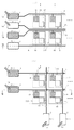
図1(a)は実施の形態1、図1(b)は実施の形態2を示し、いずれも延設配線及び検査用端子の模式図を示す。これらの図においてチップ領域24Aは、既述した図22及び図23の樹脂チップ24として切り出す前の状態を示している。なお、これらの図において電極パッド16(既述の27に対応)、電極パッド49(既述の26に対応)の形状は図22及び図23と同一形状に図示している。また、実施の形態2とことわり書きがない限り、実施の形態1の例として説明する。
【0077】
実施の形態1は図1(a)に示すように、検査用端子(+)1及び検査用端子(−)2を絶縁材の同一側縁に設けた例であり、各チップ領域24Aに形成した電極パッド49から配線3bを、電極パッド16から配線3aをそれぞれ延設し、延設配線が検査用端子1又は2まで導かれている。チップ領域には電極パッド16、49が接続される発光素子(以下、発光ダイオードと称することがある。)が存在しているが、図示省略している。図1(b)も同様。
【0078】
また、実施の形態2は図1(b)に示すように、検査用端子(+)1及び検査用端子(−)2を絶縁材の異なる側縁に設けた例であり、図1(a)と同様に各チップ領域24Aに形成した電極パッド49から配線3bを、電極パッド16から配線3aを夫々延設し、延設配線が検査用端子1又は2まで導かれている。
【0079】
これらの製造工程を以下に説明するが、既述した先願発明の製造工程と同一の工程(図2以前の工程)は省略した。即ち、図26以降の工程に対応する製造工程で本実施の形態を説明する。
【0080】
即ち、先願発明における図16〜20の工程を経て作製された発光ダイオード22が、図25に示すように選択的なレーザ照射によって一時保持用部材43の接着材層45に保持された状態を図2は示している。
【0081】
図2に示すように、発光ダイオード22が第1の一時保持用部材43の接着剤層45に保持され、発光ダイオード22の裏面はn電極側(カソード電極側)であるため、その裏面には樹脂(接着剤)がないように除去、洗浄されており、この面にカソード側のn電極パッド16を形成し、更にこの電極パッド16から配線3aを延設して不図示の検査用端子へ導く。
【0082】
接着剤層45の洗浄は先願発明と同様(図25参照)に、例えば酸素プラズマで接着剤用樹脂をエッチング、UVオゾン照射にて洗浄する。かつ、レーザにてGaN系発光ダイオードをサファイア基板からなる第一基板30から剥離したときには、その剥離面にGaが析出しているため、そのGaをエッチングすることが必要であり、NaOH水溶液若しくは希硝酸で行う。
【0083】
カソード側の電極パッドは約60μm角とすることができる。電極パッド16としては透明電極(ITO、ZnO系など)若しくはTi/Al/Pt/Auなどの材料を用いる。透明電極は発光ダイオードの発光をさえぎることがないので、パターニング精度が粗く、大きな電極形成ができ、パターニングプロセスが容易になる
【0084】
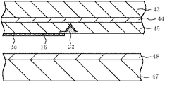
延設配線3aを形成後、この面を図3に示すように、接着剤層48を介して第2の一時保持用部材47に接着する。続いて図4に示すように、この反対側面の第1の一時保持用部材43を分離する。
【0085】
図5は、一時保持用部材43の剥離層44から発光ダイオード22を剥離して第二の一時保持用部材47に転写し、アノード電極(p電極)側のビアホール50を形成すると共に、カソード側の延設配線3aを第2の一時保持用部材47の端部に露出させ、検査用端子(−)2を形成した状態を示している。
【0086】
次に、図6に示すように、ビアホール50上にアノード側のp電極パッド49を形成し、更にこの電極パッド49の延設配線3bを設け、これを第2の一時保持用部材47の端部へ導き、この端部に検査用端子(+)1を形成する。
【0087】
本実施の形態の発光ダイオード22は、製造過程のこの段階でそれぞれの点灯検査を行うものであり、図7はこの検査状態を示している。即ち、一方の検査用端子1にプロービングパッドの端子5aが、他方の検査用端子2にプロービング端子5bを接触して検査が行われる。これにより発光ダイオード22をライン毎に検査することができる。
【0088】
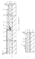
上記のように図7(図1(a)のVII−VII線断面相当)は実施の形態1を示すが、実施の形態2は図8(図1(b)のVIII−VIII線断面相当)のようになる。
【0089】
即ち、実施の形態2は、前記例のように図2の工程ではカソード側のn電極パッド16は形成されず、図6の工程においてアノード側のp電極パッド49及びその延設配線3bを形成後、図8(a)に示すように、絶縁材層45の端部の検査用端子1の領域以外を絶縁材層10で被覆し、更に発光ダイオード22に接続するスルーホール8を設けて、これにNi、Pt又はAu等を埋め込んでカソード側のn電極パッド16Aを形成し、これに延設配線3aを施し、その端部に検査用端子2を形成する。
【0090】
このように実施の形態2は、それぞれの電極パッドからの延設配線を異なる層に設けることにより、図1(b)における配線の交差部7において、正極と負極の配線が図8(b)に示すように隔設されるため、発光ダイオード22を個別に検査することができる。しかし、層を異ならせなくても、上記した図7のような構成でも絶縁材層45を挟んで配線することでも可能である。
【0091】
これらの検査により、3色LED(発光ダイオード)パネルの製造段階で輝度のばらつきの情報を収集でき、輝度を均一化するための選択データを得ることができると共に、検査時に点灯しなかった場合は、製造を中止することにより、その発光ダイオード22のその後のボンディング等の無駄な製造工程が省ける。
【0092】
図9は、発光ダイオード22を素子ごとに区分けするために、第2の一時保持用部材47を残し、ダイシングによって素子分離溝51を設けた状態を示し、図1(a)、(b)に示したダイシングライン6に沿ってダイシングされる。従って、延設配線3a、3bもこのダイシングによって同時に切断され、延設配線3a、3bを切断する特別のプロセスも必要ではない。第二の一時保持用部材47は、例えばプラスチック基板にUV粘着材が塗布された、いわゆるダイシングシートであり、UVが照射されると粘着力が低下するものを利用できる。
【0093】
このダイシングプロセスにより発光ダイオード22毎に硬化した接着剤層45を分断し、図22、23に示したような各発光ダイオード22に対応した樹脂チップ24Aが形成され、上記した延設配線3a、3bも同時に切断され、延設配線の切断面が端部に露出する。ダイシングプロセスは、機械的手段を用いたダイシング、或いはレーザビームを用いたレーザダイシングにより行い、ダイシングによる切り込み幅を、例えば20μm以下の狭い幅に切り込みが必要なときには、先願発明と同様に、上記レーザビームを用いたレーザによる加工を行うことが必要でありレーザビームとしては、エキシマレーザ、光調波YAGレーザ、炭酸ガスレーザ等を用いることができる。
【0094】
上記したプロセスは、接着剤層45の表面を酸素プラズマで発光ダイオード22の表面が露出してくるまでエッチングし、ビアホール50の形成は、やはりエキシマレーザ、高調波YAGレーザ、炭酸ガスレーザなどを用いて行うのがよい。このとき、ビアホールは約3〜7μmの径を開けることになる。アノード側電極パッドはNi、Pt又はAuなどで形成する。また、ダイシングは、例えばエキシマレーザにて幅約40μmの溝加工を行いチップ24Aを形成する。
【0095】
次に、図10に示すように、機械的手段を用いて、発光ダイオード22を埋設した樹脂チップ24Aを第二の一時保持用部材47から剥離する。第二の一時保持用部材47上の剥離層48は例えばフッ素コート、シリコーン樹脂、水溶性接着剤(例えばPVA)、ポリイミドなどを用いて形成することができる。そして、剥離層48を形成した一時保持部材47の裏面から例えばYAG第3高調波レーザを照射する。これにより、例えば剥離層48としてポリイミドを形成した場合では、ポリイミドと石英基板の界面でポリイミドのアブレーションにより剥離が発生して、各発光ダイオード22は第二の一時保持部材47から上記機械的手段により容易に剥離可能となる。
【0096】
図10は、第二の一時保持用部材47上に配列した発光ダイオード22を吸着装置53でピックアップする状態を示す図である。このときの吸着孔55が画像表示装置の画素ピッチにマトリクス状に開口しているため、発光ダイオード22を多数個、一括で吸着できる。この開口径は、例えば約φ100μmで600μmピッチのマトリクス状に開口され、一度に約300個を吸着できる。
【0097】
この吸着孔55の部材は例えば、Ni電鋳により作製したもの、若しくはステンレス(SUS)などの金属板52をエッチングで穴加工したものを使用する。金属板52の吸着孔45の奥には、吸着チャンバ54が形成されており、この吸着チャンバ54を負圧に制御することで発光ダイオード22の吸着が可能である。発光ダイオード22はこの段階では接着剤層45で覆われており、その上面は略平坦化されているため、吸着装置53による選択的な吸着を容易に進めることができる。
【0098】
図11は発光ダイオード22を第二基板60に転写する状態を示す図である。第二基板60に装着する際には第二基板60に予め接着剤層56を塗布しておき、その発光ダイオード22下面の接着剤層56を硬化させ、発光ダイオード22を第二基板60に固着する。この装着時には、吸着装置53の吸着チャンバ54が圧力の高い状態となり、吸着装置53と発光ダイオード22との吸着による結合が解除され、発光ダイオード22は第二基板60側に転写される。接着剤層56はUV硬化型接着剤、熱硬化性接着剤、熱可塑性接着剤等を用いることができる。
【0099】
発光ダイオード22を配置する位置は、一時保持用部材43、47上での配列よりも離間した位置にする。そのとき接着剤層56の樹脂を硬化させるエネルギーは第二基板60の裏面から供給する。UV硬化型接着剤の場合はUV照射装置にて、熱硬化性接着剤の場合はレーザにて発光ダイオード22の下面のみ硬化させ、熱可塑性接着剤の場合は、同様にレーザ照射にて接着剤を溶融させて接着を行う。
【0100】
また、第二基板60上にシャドウマスクとしても機能する電極層57を配設し、特に電極層57の画面側の表面、即ちこの表示装置を見る人がいる側の面に黒クロム層58を形成する。これにより画像のコントラストを向上させることができると共に、黒クロム層58でのエネルギー吸収率を高くして、選択的に照射するビーム73によって接着剤層56を早く硬化することができる。この転写時のUV照射としては、UV硬化型接着剤の場合は約1000mJ/cm2を照射するのがよい。
【0101】
図12はR、G、Bの3色の発光ダイオード22、61、62を第二基板60に配列し、絶縁層59を塗布した状態を示す図である。この場合、上記した吸着装置53を使用して、第二基板60にマウントする位置をその色の位置にずらすだけでマウントすると、画素としてのピッチは一定のまま3色からなる画素を形成できる。絶縁層59としては透明エポキシ接着剤、UV硬化型接着剤、ポリイミドなどを用いることができる。3色の発光ダイオード22、61、62は必ずしも同じ形状でなくともよい。
【0102】
図12では赤色の発光ダイオード61が六角錐のGaN層を有しない構造であり、他の発光ダイオード22、62とその形状が異なっているが、この段階では各発光ダイオード22、61、62を既に樹脂形成チップとして樹脂43で覆われているものの、素子構造の違いにもかかわらず同一の取り扱いが実現できる。
【0103】
次に、図13に示すように、発光ダイオード22の電極パッド16、49や第二基板60上の電極層57に対応して、これらを電気的に接続するために開口部(ビアホール)65、66、67、68、69、70を形成し、さらに配線を形成する。この開口部の形成も例えばレーザビームを用いて行う。
【0104】
この開口部(即ちビアホール)は、発光ダイオード22、61、62の電極パッド16、49の面積を大きくしているので、ビアホール形状は大きく、ビアホールの位置精度も各発光ダイオードに直接形成するビアホールに比べて粗い精度で形成できる。例えば、このビアホールは約60μm角の電極パッド16、49に対し、約φ20μmのものを形成できる。また、ビアホールの深さは配線基板と接続するもの、アノード電極と接続するもの、カソード電極と接続するものの3種類の深さがあるので、形成に当たっては例えばレーザのパルス数でこれを制御し、最適な深さを開口する。
【0105】
絶縁層59に開口部65、66、67、68、69、70を形成した後、発光ダイオード16、61、62のアノード、カソードの電極パッドと第二基板60の配線用の電極層57を接続する配線63、64、71を形成する。その後、保護層を配線上に形成し、画像表示装置のパネルが完成する。この保護層は図29の絶縁層59と同様、透明エポキシ接着剤などの材料が使用できる。この保護層を加熱硬化し配線を完全に覆うが、これにより、各発光ダイオード22が製品化前に点灯検査されているため、良好な発光ダイオード22を内蔵したパネル端部の配線からドライバーICを接続して良好な駆動パネルを製作することができる。
【0106】
図14は実施の形態2の例であり、検査用端子の正極及び負極を絶縁材の異なる側縁に設けて点灯検査(図8参照)を行った発光ダイオード22の場合であり、上記した図13とは一部分が異なる。即ち、図8のような構成を基に上記と同様の製造工程において、実施の形態2に対応する工程で製造されるため、図13における絶縁層10の上に、更に絶縁層59が設けられて電極パッド16Aが被覆され、この電極16Aをスルーホール11を介して外部へ引き出し、配線71に接続されることが異なるが、図13と同様に機能する。
【0107】
上述したような発光素子の配列方法により、先願発明と同様に一時保持用部材43に発光ダイオード22を保持させた時点で既に、素子間の距離が大きくされ、その広がった間隔を利用して比較的サイズの大きい電極パッド16、49などを設けることが可能となる。それら比較的サイズの大きな電極パッド16、49を利用した配線が行われるために、素子サイズに比較して最終的な装置のサイズが著しく大きな場合であっても容易に配線を形成できる。
【0108】
また、本実施の形態の発光素子の配列方法では、発光ダイオード22の周囲が硬化した接着剤層45で被覆され、平坦化によって精度良く電極パッド16、49を形成できると共に、素子に比べて広い領域に電極パッド16、49を延在でき、次の第二転写工程での転写を吸着治具で進める場合には取り扱いが容易になる。
【0109】
本実施の形態によれば、発光ダイオード22の製造段階でアノード側及びカソード側の配線16、49に延設配線3a、3bを設け、これを検査用端子1、2へ導き、製品化前に点灯検査ができるので、3色LEDパネルを作製する前に各LEDの輝度ばらつきの情報を収集でき、均一な輝度の画面にするためのLED選択のデータにできると共に、点灯しなかった場合は製造を中止して、不良品はボンディング等のその後の無駄な工程を省くことができる。また、延設した配線は、その後の必須なダイシング工程で同時に切断するので特別なプロセスも必要でない。
【0110】
上記した本発明の実施の形態は、本発明の技術的思想に基づいて変形することができる。
【0111】
例えば、実施の形態の回路素子は発光ダイオードの例としたが、それ以外に、液晶制御素子、光電変換素子、圧電素子、薄膜トランジスタ素子、薄膜ダイオード素子、半導体レーザ、抵抗素子、スイッチング素子、微小磁気素子、微小光学素子等にも適用することができる。また、素子22の大きさとしては、実施の形態以外の大きさにすることもできる。
【0112】
また、検査用端子1及び2の形状や設置場所、配線の延設方法、積層構造、製造プロセス等も実施の形態以外の適宜に実施することも可能である。
【0113】
【発明の作用効果】
上述した如く、本発明の回路素子の検査方法及びその検査構造、回路素子内蔵基板及びその製造方法、並びに電気回路装置及びその製造方法は、絶縁材に回路素子を埋設した状態で、この回路素子の電極に接続した配線を検査用端子まで延設し、この検査用端子を介して検査するので、半製品の如き状態でこの検査をすることにより、製品化以前の段階で回路素子の特性の情報が得られ、特性の均一化された回路素子を選択することができる。
【図面の簡単な説明】
【図1】本発明の実施の形態による検査用端子形成の一例を示す模式図であり、(a)は実施の形態1、(b)は実施の形態2である。
【図2】同、実施の形態1による回路素子内蔵基板の製造工程の一工程を示す概略図である。
【図3】同、実施の形態1による回路素子内蔵基板の製造工程の他の一工程を示す概略図である。
【図4】同、実施の形態1による回路素子内蔵基板の製造工程の他の一工程を示す概略図である。
【図5】同、実施の形態1による回路素子内蔵基板の製造工程の他の一工程を示す概略図である。
【図6】同、実施の形態1による回路素子内蔵基板の製造工程の他の一工程を示す概略図である。
【図7】同、実施の形態1による回路素子内蔵基板の製造工程の他の一工程を示す概略図である。
【図8】同、実施の形態2による回路素子内蔵基板の製造工程の一工程を示す概略図である。
【図9】同、実施の形態1による回路素子内蔵基板の製造工程の一工程を示す概略図である。
【図10】同、実施の形態1による回路素子内蔵基板の製造工程の一工程を示す概略図である。
【図11】同、実施の形態1による電気回路装置の製造工程の一工程を示す概略図である。
【図12】同、実施の形態1による電気回路装置の製造工程の他の一工程を示す概略図である。
【図13】同、実施の形態1による電気回路装置の製造工程の更に他の一工程を示す概略図である。
【図14】同、実施の形態2による電気回路装置の製造工程の一工程を示す概略図である。
【図15】先願発明による回路素子内蔵基板の製造工程の一工程を示す概略図である。
【図16】同、回路素子内蔵基板の製造工程の他の一工程を示す概略図である。
【図17】同、回路素子内蔵基板の製造工程の他の一工程を示す概略図である。
【図18】同、回路素子内蔵基板の製造工程の他の一工程を示す概略図である。
【図19】同、回路素子内蔵基板の製造工程の他の一工程を示す概略図である。
【図20】図19の一部分の拡大図である。
【図21】図20の詳細図であり、(a)は一部分の断面図、(b)は平面図である。
【図22】先願発明による回路素子内蔵基板の製造段階における状態を模式的に示した斜視図である。
【図23】図22の平面図である。
【図24】先願発明による回路素子の内蔵基板の製造工程の一工程を示す概略図である。
【図25】先願発明による回路素子の内蔵基板の製造工程の一工程を示す概略図である。
【図26】先願発明による回路素子の内蔵基板の製造工程の一工程を示す概略図である。
【図27】先願発明による回路素子の内蔵基板の製造工程の一工程を示す概略図である。
【図28】先願発明による回路素子の内蔵基板の製造工程の一工程を示す概略図である。
【図29】先願発明による回路素子の内蔵基板の製造工程の一工程を示す概略図である。
【図30】先願発明による回路素子の内蔵基板の製造工程の更に他の一工程を示す概略図である。
【符号の説明】
1…検査用端子(+)、2…検査用端子(−)、3a、3b…延設配線、
5a、5b…プロービング端子、6…ダイシングライン、7…交差部、
8、11…スルーホール、9…配線、
10、45、48…接着剤層(絶縁材層)、
16、16A、26、27、49…電極パッド、
22、61、62…素子(発光ダイオード)、23…樹脂、
24、24A…樹脂チップ、30…サファイア基板(第1基板)、
31、33…GaN層、32…マスク、34…InGaN層、
35…MaGaN層、37p電極、42g…溝、43…第1保持用部材、
44…剥離層、45s…硬化領域、45y…未硬化領域、
46、73…レーザ光、47…第2保持用部材、53…吸着装置、
59…絶縁層、60…第2基板[0001]
BACKGROUND OF THE INVENTION
The present invention relates to a circuit element inspection method and inspection structure suitable for inspection of a light emitting element used in an image display device, for example, a circuit element built-in substrate and a manufacturing method thereof, and an electric circuit device and a manufacturing method thereof. .
[0002]
[Prior art]
As a semiconductor light emitting device, a low-temperature buffer layer and an n-side contact layer made of Si-doped GaN have been formed on the entire surface of a sapphire substrate, and an n-side clad layer made of Si-doped GaN and Si doped therein. A device is known in which an active layer made of InGaN, a p-side cladding layer made of Mg-doped AlGaN, a p-side contact layer made of Mg-doped GaN, and the like are stacked. As products that have such a structure and are commercially available, blue and green LEDs (Light Emitting Diodes) including 450 nm to 530 nm are mass-produced.
[0003]
In addition, when trying to grow gallium nitride, a sapphire substrate is often used. Usually, a sapphire substrate having a C-plane as a main surface is used, and the surface of the gallium nitride layer formed on the main surface is also used. An active layer having a C plane and necessarily formed on a plane parallel to the main surface of the substrate and a clad layer sandwiching the active layer also extend to a plane parallel to the C plane. As described above, in the semiconductor light emitting device having a structure in which each crystal layer is laminated with the substrate main surface as a reference, smoothness necessary for electrode formation or the like is obtained by utilizing the smoothness of the substrate main surface.
[0004]
However, there are problems such as generation of crystal defects due to lattice mismatch between the sapphire substrate and the gallium nitride to be grown, difficulty in cutting out a fine chip, high manufacturing cost, and poor productivity.
[0005]
[Course to Invention]
In order to solve such a problem, the applicant of the present invention has good crystallinity, can be miniaturized, can be modularized while suppressing manufacturing cost, and can be easily transported and mounted on a substrate. A display element and a method for manufacturing the same have already been proposed in Japanese Patent Application No. 2001-144452.
[0006]
This display element (hereinafter referred to as the prior application invention) has a structure shown in FIG. 30, for example. That is, for example, in the case of the
[0007]
In the manufacturing method, as shown in FIG. 15, a buffer layer of either AlN or GaN is first formed at a low temperature of 500 ° C. on a
[0008]
Next, as shown in FIG. 16, the GaN
[0009]
Next, as shown in FIG. 17, the
[0010]
When the size of the hexagonal pyramid is, for example, about 15 to 20 μm in width (one side is about 7.5 to 15 μm), the height is about 1.6 times that side (ie, about 10 to 16 μm) as a hexagonal cone. Become. The size of the hexagonal pyramid can be about 10 μm in width.
[0011]
Next, the growth temperature is reduced, and an InGaN
[0012]
Next, as shown in FIG. 19, a p-
[0013]
FIG. 20 shows an enlarged view of one light emitting element (hereinafter sometimes referred to as a light emitting diode) 22 manufactured in the above manufacturing process. As shown in the figure, the configuration has a silicon-doped
[0014]
As shown in FIG. 21A, which is a cross-sectional view of only the
[0015]
The light-emitting
[0016]
These light-emitting
[0017]
That is, as shown in FIG. 23, the
[0018]
[0019]
Here, the
[0020]
By configuring such a
[0021]
Next, a method for arranging the
[0022]
The light-emitting
[0023]
A
[0024]
As the
[0025]
The
[0026]
After such alignment, the
[0027]
As a result of peeling using this laser ablation, the
[0028]
In FIG. 24, only one
[0029]
The
[0030]
For example, the
[0031]
At this time, the electrode pad on the cathode side can be about 60 μm square. The
[0032]
After the
[0033]
In FIG. 26, the light-emitting
[0034]
As a result of this dicing, an
[0035]
As an example of this process, the surface of the
[0036]
Next, as shown in FIG. 27, the light emitting diode 22 (resin chip 24) is peeled from the second temporary holding
[0037]
FIG. 27 is a view showing a state in which the
[0038]
As the member of the
[0039]
FIG. 28 is a view showing a state where the
[0040]
The position where the
[0041]
In addition, an
[0042]
FIG. 29 is a view showing a state in which the
[0043]
In FIG. 29, the red light-emitting
[0044]
Next, as shown in FIG. 30, corresponding to the
[0045]
The opening formed at this time, that is, the via hole, increases the area of the
[0046]
After the
[0047]
In the arrangement method of the light emitting elements as described above, as shown in FIG. 25, the distance between the elements is already increased at the time when the
[0048]
Further, in the light emitting element arrangement method of this example, the periphery of the
[0049]
As described above, according to the invention of the prior application, by embedding the light-emitting element in an insulating material, the light-emitting element is re-formed into a size that is easy to handle and modularized, so that handling properties can be ensured while reducing manufacturing costs. For example, the display element can be easily transported, and the drive electrode of the light emitting element is drawn out on the surface of the modularized display element, so that the power supply line and signal line formed on the substrate can be easily connected. It can be connected to these drive electrodes, and mounting on a substrate is very easy.
[0050]
[Problems to be solved by the invention]
However, although the prior invention has the above-described features, it has been found that there are still problems to be improved.
[0051]
That is, because the design and structure cannot be inspected when the light emitting device according to the invention of the prior application is embedded in the insulating layer, the lighting inspection in that state cannot be performed, and in the embedded state in the brightness variation of the LED or the insulating material. No information on whether or not the pad electrode was defective could not be obtained. For this reason, when the product is not turned on or the luminance is not uniform, the product must be discarded, resulting in a decrease in yield.
[0052]
SUMMARY OF THE INVENTION Accordingly, an object of the present invention is to inspect a circuit element and its inspection structure in a state before commercialization of the circuit element while maintaining the features of the invention of the prior application, a circuit element built-in substrate and its manufacturing method, and an electric circuit. It is to provide an apparatus and a manufacturing method thereof.
[0053]
[Means for Solving the Problems]
That is, the present invention extends the wiring connected to the electrode of the circuit element in a state where the circuit element is embedded in the insulating material to the inspection terminal, and inspects the characteristics of the circuit element through the inspection terminal. The present invention relates to a circuit element inspection method (hereinafter referred to as the inspection method of the present invention).
[0054]
According to the inspection method of the present invention, in the state where the circuit element is embedded in the insulating material, the wiring connected to the electrode of the circuit element is extended to the inspection terminal, and the inspection is performed through the inspection terminal. By inspecting in the state of the product, information on the characteristics of the circuit elements can be obtained at a stage before commercialization, and the circuit elements having uniform characteristics can be selected.
[0055]
Further, the present invention provides a circuit element inspection structure (hereinafter referred to as the present invention) in which a wiring connected to an electrode of the circuit element is extended to the circuit element characteristic inspection terminal in a state where the circuit element is embedded in an insulating material. (Referred to as the inspection structure of the invention).
[0056]
According to the inspection structure of the present invention, since the structure is based on the above-described inspection method of the present invention, it is possible to provide an inspection structure that exhibits the same effect as the inspection method of the present invention.
[0057]
The present invention also relates to a circuit element built-in substrate (hereinafter referred to as a circuit element built-in substrate of the present invention) in which the above-described inspection structure is provided on the substrate.
[0058]
According to the circuit element built-in substrate of the present invention, since the above-described inspection structure of the present invention is provided on the substrate, the circuit element sufficiently characterized by the inspection method of the present invention is incorporated. It is possible to provide a circuit element-embedded substrate that can provide the same effects as the inspection method.
[0059]
In addition, the present invention, when manufacturing the circuit element built-in substrate described above,
Embedding a circuit element in an insulating material;
Bonding the insulating material surface opposite to the embedded surface of the circuit element to a first holding member;
After separating the insulating material in which the circuit element is embedded from the first holding member, providing a wiring for taking out one electrode of the circuit element and extending the wiring to one inspection terminal When,
Providing a lead-out wiring on the other electrode of the circuit element and extending the wiring to the other inspection terminal;
The circuit element built-in substrate manufacturing method (hereinafter referred to as the circuit element built-in substrate manufacturing method of the present invention) having the above.
[0060]
According to the method for manufacturing a circuit element-embedded substrate of the present invention, the circuit element-embedded substrate having the above-described inspection structure of the present invention can be obtained. A method can be provided.
[0061]
In the present invention, the circuit element is embedded in an insulating material, and the wiring connected to the electrode of the circuit element extends to the side end of the insulating material and is exposed here, and the wiring is further connected to the wiring circuit. The present invention relates to an electric circuit device (hereinafter referred to as an electric circuit device of the present invention) connected to a substrate.
[0062]
According to the electric circuit device of the present invention, since the circuit element is formed based on the above-described inspection structure of the present invention, the characteristics can be sufficiently inspected by the above-described inspection method of the present invention, and similar effects can be obtained. An electric circuit device having circuit elements to be played can be provided.
[0063]
Further, the present invention, when manufacturing an electric circuit device having a circuit element of the inspection structure of the present invention described above,
A step of obtaining a circuit element built-in substrate by the manufacturing method of the inspection structure described above;
Inspecting the characteristics of the circuit element via the inspection terminal;
After the inspection, cutting between the electrode and the inspection terminal, and chipping the insulating material embedded with the circuit element,
Fixing the chip to the printed circuit board;
Connecting the wiring to the wired circuit board;
This invention relates to a method for manufacturing an electric circuit device (hereinafter referred to as a method for manufacturing an electric circuit device of the present invention).
[0064]
According to the method for manufacturing the electric circuit device of the present invention, the circuit element having the above-described inspection structure is formed into a chip and connected to the printed circuit board after the inspection of the characteristics by the above-described inspection method. It is possible to provide a method of manufacturing an electric circuit device with good reproducibility that has an effect.
[0065]
DETAILED DESCRIPTION OF THE INVENTION
Hereinafter, preferred embodiments of the present invention will be described.
[0066]
In the inspection method, inspection structure, circuit element built-in substrate, circuit element built-in substrate manufacturing method, electric circuit device, and electric circuit device manufacturing method according to the present invention described above, the circuit element is embedded on the insulating material. A wiring for taking out one electrode of the circuit element is provided on the surface of the circuit element, and a wiring for taking out the other electrode of the circuit element is provided on the other side of the circuit element. It is desirable that the test terminal is extended to the inspection terminal and inspected by contacting the probing terminal with the inspection terminal.
[0067]
And after the said test | inspection, it is desirable to cut | disconnect between the said electrode and the said test | inspection terminal, and to chip-form the said insulating material which embed | buried the said circuit element.
[0068]
In this case, the positive electrode and the negative electrode of the inspection terminal may be provided on the same side edge of the insulating material, and the positive electrode and the negative electrode of the inspection terminal may be provided on different side edges of the insulating material, respectively.
[0069]
When the positive electrode and the negative electrode of the inspection terminal are provided on the same side edge, it is desirable that the wiring connected to the one electrode and the wiring connected to the other electrode are provided on the same insulating material.
[0070]
In addition, when the positive electrode and the negative electrode of the inspection terminal are provided on different side edges, an insulating layer is formed on the wiring connected to the one electrode and the wiring connected to the other electrode, and on the insulating layer It is desirable to provide the inspection terminal in
[0071]
Then, it is desirable to transfer the circuit element from the base and inspect the characteristics of the circuit element embedded in the insulating material.
[0072]
In this case, it is desirable to hold the insulating material in which the circuit element is embedded on the substrate before the transfer.
[0073]
And the characteristic of the said circuit element can be test | inspected for every line or / and individually, and the lighting test | inspection of the circuit element which is a light emitting element can be performed.
[0074]
Accordingly, it is possible to satisfactorily perform a lighting inspection of the light emitting element used in the image display device or the light source device in which the wiring is led to the circuit wiring board through the insulating layer provided on the insulating material. .
[0075]
The above-described preferred embodiment of the present invention will be specifically described.
[0076]
FIG. 1A shows the first embodiment, and FIG. 1B shows the second embodiment, both of which are schematic diagrams of the extended wiring and the inspection terminal. In these drawings, a
[0077]
As shown in FIG. 1A, the first embodiment is an example in which an inspection terminal (+) 1 and an inspection terminal (−) 2 are provided on the same side edge of an insulating material, and are formed in each
[0078]
The second embodiment is an example in which the inspection terminal (+) 1 and the inspection terminal (−) 2 are provided on different side edges of the insulating material as shown in FIG. ), The
[0079]
These manufacturing steps will be described below, but the same steps (the steps before FIG. 2) as the manufacturing steps of the prior invention described above are omitted. In other words, the present embodiment will be described in the manufacturing process corresponding to the processes from FIG.
[0080]
That is, the state where the
[0081]
As shown in FIG. 2, the
[0082]
Cleaning of the
[0083]
The electrode pad on the cathode side can be about 60 μm square. The
[0084]
After the
[0085]
FIG. 5 shows that the
[0086]
Next, as shown in FIG. 6, an anode-side p-
[0087]
The
[0088]
As described above, FIG. 7 (corresponding to the section taken along line VII-VII in FIG. 1A) shows the first embodiment, while
[0089]
That is, in the second embodiment, the cathode-side n-
[0090]
As described above, in the second embodiment, the wirings extending from the respective electrode pads are provided in different layers, so that the positive and negative wirings are connected to each other at the
[0091]
By these inspections, it is possible to collect information on luminance variations at the manufacturing stage of a three-color LED (light emitting diode) panel, obtain selection data for uniforming the luminance, and if it does not light during inspection By canceling the manufacturing, useless manufacturing processes such as subsequent bonding of the
[0092]
FIG. 9 shows a state in which the second temporary holding
[0093]
By this dicing process, the cured
[0094]
In the above process, the surface of the
[0095]
Next, as shown in FIG. 10, the
[0096]
FIG. 10 is a diagram illustrating a state in which the
[0097]
As the member of the
[0098]
FIG. 11 is a diagram illustrating a state where the
[0099]
The position where the
[0100]
In addition, an
[0101]
FIG. 12 is a view showing a state in which the
[0102]
In FIG. 12, the red
[0103]
Next, as shown in FIG. 13, corresponding to the
[0104]
This opening (ie, via hole) increases the area of the
[0105]
After the
[0106]
FIG. 14 shows an example of the second embodiment, which is a case of the light-emitting
[0107]
By the method for arranging the light emitting elements as described above, the distance between the elements is already increased at the time when the
[0108]
Further, in the light emitting element arrangement method of the present embodiment, the periphery of the
[0109]
According to the present embodiment, the
[0110]
The above-described embodiment of the present invention can be modified based on the technical idea of the present invention.
[0111]
For example, the circuit element of the embodiment is an example of a light emitting diode, but in addition to that, a liquid crystal control element, a photoelectric conversion element, a piezoelectric element, a thin film transistor element, a thin film diode element, a semiconductor laser, a resistance element, a switching element, a micro magnetism The present invention can also be applied to elements, micro optical elements, and the like. Also, the size of the
[0112]
Further, the shapes and installation locations of the
[0113]
[Effects of the invention]
As described above, the circuit element inspection method and the inspection structure thereof, the circuit element built-in substrate and the manufacturing method thereof, and the electric circuit device and the manufacturing method thereof according to the present invention include the circuit element embedded in an insulating material. The wiring connected to the electrodes is extended to the inspection terminal and inspected through this inspection terminal. By performing this inspection in the state of a semi-finished product, the characteristics of circuit elements can be Information can be obtained, and circuit elements with uniform characteristics can be selected.
[Brief description of the drawings]
FIGS. 1A and 1B are schematic views showing an example of forming an inspection terminal according to an embodiment of the present invention, where FIG. 1A is Embodiment 1 and FIG. 1B is
FIG. 2 is a schematic diagram showing one process of manufacturing a circuit element built-in substrate according to the first embodiment.
FIG. 3 is a schematic view showing another step of the manufacturing process of the circuit element built-in substrate according to the first embodiment;
4 is a schematic view showing another process of the manufacturing process of the circuit element built-in substrate according to the first embodiment. FIG.
FIG. 5 is a schematic view showing another process of the circuit element built-in substrate according to the first embodiment.
FIG. 6 is a schematic view showing another process of manufacturing the circuit element built-in substrate according to the first embodiment.
FIG. 7 is a schematic view showing another process of manufacturing the circuit element built-in substrate according to the first embodiment.
FIG. 8 is a schematic diagram showing one process of manufacturing a circuit element built-in substrate according to the second embodiment.
FIG. 9 is a schematic diagram showing one process of manufacturing a circuit element built-in substrate according to the first embodiment.
FIG. 10 is a schematic diagram showing one process of manufacturing a circuit element built-in substrate according to the first embodiment.
FIG. 11 is a schematic diagram showing one process of manufacturing the electric circuit device according to the first embodiment.
FIG. 12 is a schematic diagram showing another step of the manufacturing process of the electric circuit device according to the first embodiment.
FIG. 13 is a schematic diagram showing still another process of the manufacturing process of the electric circuit device according to the first embodiment.
FIG. 14 is a schematic view showing one process of manufacturing an electric circuit device according to the second embodiment.
FIG. 15 is a schematic view showing one process of manufacturing a circuit element built-in substrate according to the invention of the prior application.
FIG. 16 is a schematic view showing another process of manufacturing the circuit element built-in substrate.
FIG. 17 is a schematic view showing another process of manufacturing the circuit element built-in substrate.
FIG. 18 is a schematic view showing another process of manufacturing the circuit element built-in substrate.
FIG. 19 is a schematic view showing another process of manufacturing the circuit element built-in substrate.
20 is an enlarged view of a part of FIG.
FIG. 21 is a detailed view of FIG. 20, in which (a) is a partial cross-sectional view and (b) is a plan view.
FIG. 22 is a perspective view schematically showing a state in a manufacturing stage of the circuit element built-in substrate according to the prior application invention.
FIG. 23 is a plan view of FIG. 22;
FIG. 24 is a schematic view showing one process of manufacturing a circuit element built-in substrate according to the prior invention.
FIG. 25 is a schematic view showing one process of manufacturing a circuit element built-in substrate according to the prior invention.
FIG. 26 is a schematic diagram showing one process of manufacturing a circuit element built-in substrate according to the prior invention.
FIG. 27 is a schematic view showing one process of manufacturing a circuit element built-in substrate according to the prior invention.
FIG. 28 is a schematic view showing one process of manufacturing a circuit element built-in substrate according to the prior invention.
FIG. 29 is a schematic diagram showing one process of manufacturing a circuit element built-in substrate according to the invention of the prior application.
FIG. 30 is a schematic view showing still another process of manufacturing a circuit element built-in substrate according to the invention of the prior application.
[Explanation of symbols]
DESCRIPTION OF SYMBOLS 1 ... Inspection terminal (+), 2 ... Inspection terminal (-), 3a, 3b ... Extension wiring,
5a, 5b ... probing terminals, 6 ... dicing lines, 7 ... intersections,
8, 11 ... through hole, 9 ... wiring,
10, 45, 48 ... adhesive layer (insulating material layer),
16, 16A, 26, 27, 49 ... electrode pads,
22, 61, 62 ... element (light emitting diode), 23 ... resin,
24, 24A ... resin chip, 30 ... sapphire substrate (first substrate),
31, 33 ... GaN layer, 32 ... mask, 34 ... InGaN layer,
35 ... MaGaN layer, 37p electrode, 42g ... groove, 43 ... first holding member,
44 ... peeling layer, 45s ... cured region, 45y ... uncured region,
46, 73 ... laser light, 47 ... second holding member, 53 ... suction device,
59 ... Insulating layer, 60 ... Second substrate
Claims (18)
回路素子を絶縁材に埋設させる工程と、
前記回路素子の埋設面とは反対側の前記絶縁材面を第1保持用部材に接着する工程と 、
前記第1保持用部材から、前記回路素子を埋設した前記絶縁材を分離した後に、前記 回路素子の一方の電極の取り出し用配線を設け、かつこの配線を一方の検査用端子まで 延設する工程と、
前記回路素子の他方の電極に取り出し用配線を設け、かつこの配線を他方の検査用端 子まで延設する工程と
を有する、回路素子内蔵基板の製造方法。When manufacturing a circuit element built-in substrate,
Embedding a circuit element in an insulating material;
Bonding the insulating material surface opposite to the embedded surface of the circuit element to the first holding member;
After separating the insulating material in which the circuit element is embedded from the first holding member, providing a wiring for taking out one electrode of the circuit element and extending the wiring to one inspection terminal When,
A method of manufacturing a circuit element-embedded substrate, comprising: providing a wiring for extraction on the other electrode of the circuit element, and extending the wiring to the other inspection terminal.
請求項1〜8のいずれか1項に記載した製造方法によって回路素子内蔵基板を得る工 程と、
前記検査用端子を介して前記回路素子の特性を検査する工程と、
前記検査後に、前記電極と前記検査用端子との間を切断して、前記回路素子を埋設し た前記絶縁材をチップ化する工程と、
前記チップを配線回路基板に固定する工程と、
前記配線を前記配線回路基板に接続する工程と
を有する、電気回路装置の製造方法。When manufacturing electrical circuit devices,
A process of obtaining a circuit element-embedded substrate by the manufacturing method according to any one of claims 1 to 8 ;
Inspecting the characteristics of the circuit element via the inspection terminal;
After the inspection, the step of cutting between the electrode and the inspection terminal to chip the insulating material embedded with the circuit element;
Fixing the chip to the printed circuit board;
Connecting the wiring to the printed circuit board.
Priority Applications (1)
| Application Number | Priority Date | Filing Date | Title |
|---|---|---|---|
| JP2001268950A JP4876356B2 (en) | 2001-09-05 | 2001-09-05 | Method for manufacturing circuit element built-in substrate and method for manufacturing electric circuit device |
Applications Claiming Priority (1)
| Application Number | Priority Date | Filing Date | Title |
|---|---|---|---|
| JP2001268950A JP4876356B2 (en) | 2001-09-05 | 2001-09-05 | Method for manufacturing circuit element built-in substrate and method for manufacturing electric circuit device |
Publications (2)
| Publication Number | Publication Date |
|---|---|
| JP2003078170A JP2003078170A (en) | 2003-03-14 |
| JP4876356B2 true JP4876356B2 (en) | 2012-02-15 |
Family
ID=19094856
Family Applications (1)
| Application Number | Title | Priority Date | Filing Date |
|---|---|---|---|
| JP2001268950A Expired - Fee Related JP4876356B2 (en) | 2001-09-05 | 2001-09-05 | Method for manufacturing circuit element built-in substrate and method for manufacturing electric circuit device |
Country Status (1)
| Country | Link |
|---|---|
| JP (1) | JP4876356B2 (en) |
Cited By (1)
| Publication number | Priority date | Publication date | Assignee | Title |
|---|---|---|---|---|
| CN106935570A (en) * | 2017-03-31 | 2017-07-07 | 京东方科技集团股份有限公司 | Test circuit, method of testing, array base palte and its manufacture method |
Families Citing this family (11)
| Publication number | Priority date | Publication date | Assignee | Title |
|---|---|---|---|---|
| DE102009051746A1 (en) | 2009-09-30 | 2011-03-31 | Osram Opto Semiconductors Gmbh | Optoelectronic component |
| JP4955792B2 (en) * | 2010-04-28 | 2012-06-20 | シャープ株式会社 | Electronic component operation function measuring apparatus and electronic component operation function measuring method |
| JP2012190905A (en) * | 2011-03-09 | 2012-10-04 | Hitachi Cable Ltd | Method of manufacturing semiconductor light-emitting element |
| JP2013239548A (en) * | 2012-05-15 | 2013-11-28 | Seiko Epson Corp | Sheet substrate, electronic component, electronic apparatus, electronic component testing method and electronic component manufacturing method |
| DE102013112885A1 (en) * | 2013-11-21 | 2015-05-21 | Osram Opto Semiconductors Gmbh | Method for optically characterizing an optoelectronic semiconductor material and device for carrying out the method |
| JP6435705B2 (en) | 2013-12-27 | 2018-12-12 | 日亜化学工業株式会社 | Collective substrate, light-emitting device, and light-emitting element inspection method |
| US11172571B2 (en) | 2018-02-16 | 2021-11-09 | Kyocera Corporation | Multipiece element storage package and multipiece optical semiconductor device |
| EP3591345B1 (en) * | 2018-07-02 | 2020-11-11 | Dr. Johannes Heidenhain GmbH | Position measuring device and method for producing a light source for a sensor unit of a position measuring device |
| CN112285514A (en) * | 2019-07-09 | 2021-01-29 | 致茂电子(苏州)有限公司 | Wafer testing device |
| TWI704360B (en) * | 2019-07-09 | 2020-09-11 | 致茂電子股份有限公司 | Wafer testing device of flip chip vcsel |
| JP7319551B2 (en) * | 2020-03-31 | 2023-08-02 | 日亜化学工業株式会社 | light emitting device |
Family Cites Families (4)
| Publication number | Priority date | Publication date | Assignee | Title |
|---|---|---|---|---|
| JPS51129457A (en) * | 1975-05-06 | 1976-11-11 | Sekisui Chemical Co Ltd | Molding method and molds for insert moldings |
| JPS5533014A (en) * | 1978-08-29 | 1980-03-08 | Towa Electric | Method of and device for automatically sorting and picking up electric part |
| JPH0738405B2 (en) * | 1986-11-20 | 1995-04-26 | 日精樹脂工業株式会社 | Light emitting diode manufacturing equipment |
| JPS6459826A (en) * | 1987-08-31 | 1989-03-07 | Matsushita Electric Ind Co Ltd | Mounting of led chip |
-
2001
- 2001-09-05 JP JP2001268950A patent/JP4876356B2/en not_active Expired - Fee Related
Cited By (3)
| Publication number | Priority date | Publication date | Assignee | Title |
|---|---|---|---|---|
| CN106935570A (en) * | 2017-03-31 | 2017-07-07 | 京东方科技集团股份有限公司 | Test circuit, method of testing, array base palte and its manufacture method |
| CN106935570B (en) * | 2017-03-31 | 2019-04-26 | 京东方科技集团股份有限公司 | Test circuit, test method, array substrate and its manufacturing method |
| US10429412B2 (en) | 2017-03-31 | 2019-10-01 | Boe Technology Group Co., Ltd. | Test circuit, test method, array substrate and manufacturing method thereof |
Also Published As
| Publication number | Publication date |
|---|---|
| JP2003078170A (en) | 2003-03-14 |
Similar Documents
| Publication | Publication Date | Title |
|---|---|---|
| JP3747807B2 (en) | Device mounting substrate and defective device repair method | |
| JP4055405B2 (en) | Electronic component and manufacturing method thereof | |
| JP3906653B2 (en) | Image display device and manufacturing method thereof | |
| TW550733B (en) | Wiring method and element arranging method using the same, and method of producing image display devices | |
| JP3994681B2 (en) | Element arrangement method and image display device manufacturing method | |
| JP4876356B2 (en) | Method for manufacturing circuit element built-in substrate and method for manufacturing electric circuit device | |
| JP4734770B2 (en) | Manufacturing method of resin forming element, manufacturing method of image display device, and manufacturing method of lighting device | |
| JP3682584B2 (en) | Method for mounting light emitting element and method for manufacturing image display device | |
| JP4078825B2 (en) | Circuit board manufacturing method and display device manufacturing method | |
| JP4882273B2 (en) | Device mounting substrate, defective device repair method, and image display device | |
| JP4403434B2 (en) | Image display device | |
| JP3890921B2 (en) | Element arrangement method and image display device manufacturing method | |
| JP2003209295A (en) | Electronic component, manufacturing method therefor and image display device using the same | |
| JP4403422B2 (en) | Manufacturing method of image display device | |
| JP4982932B2 (en) | Manufacturing method of image display device | |
| JP2002344028A (en) | Method of transferring element, and method of manufacturing image display device | |
| JP4182661B2 (en) | Image display device and manufacturing method thereof | |
| JP4055817B2 (en) | Image display device | |
| JP2003005674A (en) | Display element and image display device | |
| JP4078830B2 (en) | Display device and manufacturing method of display device | |
| JP2003216072A (en) | Image display device and its manufacturing method | |
| JP4967251B2 (en) | Manufacturing method of image display device | |
| JP4848606B2 (en) | Element positioning method, element extraction method, element transfer method, element arrangement method, and image display device manufacturing method | |
| JP4839533B2 (en) | Image display device and manufacturing method thereof | |
| JP4126913B2 (en) | Semiconductor light emitting element, image display device, lighting device, and manufacturing method thereof |
Legal Events
| Date | Code | Title | Description |
|---|---|---|---|
| RD13 | Notification of appointment of power of sub attorney |
Free format text: JAPANESE INTERMEDIATE CODE: A7433 Effective date: 20070125 |
|
| A621 | Written request for application examination |
Free format text: JAPANESE INTERMEDIATE CODE: A621 Effective date: 20080707 |
|
| RD02 | Notification of acceptance of power of attorney |
Free format text: JAPANESE INTERMEDIATE CODE: A7422 Effective date: 20090526 |
|
| A977 | Report on retrieval |
Free format text: JAPANESE INTERMEDIATE CODE: A971007 Effective date: 20110608 |
|
| A131 | Notification of reasons for refusal |
Free format text: JAPANESE INTERMEDIATE CODE: A131 Effective date: 20110614 |
|
| A521 | Written amendment |
Free format text: JAPANESE INTERMEDIATE CODE: A523 Effective date: 20110719 |
|
| TRDD | Decision of grant or rejection written | ||
| A01 | Written decision to grant a patent or to grant a registration (utility model) |
Free format text: JAPANESE INTERMEDIATE CODE: A01 Effective date: 20111101 |
|
| A01 | Written decision to grant a patent or to grant a registration (utility model) |
Free format text: JAPANESE INTERMEDIATE CODE: A01 |
|
| A61 | First payment of annual fees (during grant procedure) |
Free format text: JAPANESE INTERMEDIATE CODE: A61 Effective date: 20111114 |
|
| FPAY | Renewal fee payment (prs date is renewal date of database) |
Free format text: PAYMENT UNTIL: 20141209 Year of fee payment: 3 |
|
| LAPS | Cancellation because of no payment of annual fees |