JP4868488B2 - Radio clock - Google Patents
Radio clock Download PDFInfo
- Publication number
- JP4868488B2 JP4868488B2 JP2004224662A JP2004224662A JP4868488B2 JP 4868488 B2 JP4868488 B2 JP 4868488B2 JP 2004224662 A JP2004224662 A JP 2004224662A JP 2004224662 A JP2004224662 A JP 2004224662A JP 4868488 B2 JP4868488 B2 JP 4868488B2
- Authority
- JP
- Japan
- Prior art keywords
- time
- signal
- amplitude
- duration
- time signal
- Prior art date
- Legal status (The legal status is an assumption and is not a legal conclusion. Google has not performed a legal analysis and makes no representation as to the accuracy of the status listed.)
- Active
Links
- 230000008859 change Effects 0.000 claims description 30
- 238000000034 method Methods 0.000 claims description 28
- 230000001360 synchronised effect Effects 0.000 claims description 9
- 238000004364 calculation method Methods 0.000 claims description 5
- 239000013078 crystal Substances 0.000 claims description 3
- 238000007689 inspection Methods 0.000 claims description 3
- 238000001914 filtration Methods 0.000 claims 1
- 230000005540 biological transmission Effects 0.000 description 18
- 238000010586 diagram Methods 0.000 description 16
- 238000011156 evaluation Methods 0.000 description 13
- 239000003550 marker Substances 0.000 description 12
- 230000008054 signal transmission Effects 0.000 description 11
- 239000003990 capacitor Substances 0.000 description 10
- 238000012545 processing Methods 0.000 description 4
- 230000000694 effects Effects 0.000 description 3
- 238000005516 engineering process Methods 0.000 description 3
- 230000006870 function Effects 0.000 description 3
- 230000007704 transition Effects 0.000 description 3
- 229910000859 α-Fe Inorganic materials 0.000 description 3
- 230000003321 amplification Effects 0.000 description 2
- 238000012937 correction Methods 0.000 description 2
- 238000013461 design Methods 0.000 description 2
- 238000001514 detection method Methods 0.000 description 2
- 238000005259 measurement Methods 0.000 description 2
- 238000003199 nucleic acid amplification method Methods 0.000 description 2
- 230000008569 process Effects 0.000 description 2
- 239000010453 quartz Substances 0.000 description 2
- 230000009467 reduction Effects 0.000 description 2
- VYPSYNLAJGMNEJ-UHFFFAOYSA-N silicon dioxide Inorganic materials O=[Si]=O VYPSYNLAJGMNEJ-UHFFFAOYSA-N 0.000 description 2
- 230000001960 triggered effect Effects 0.000 description 2
- 229910052792 caesium Inorganic materials 0.000 description 1
- TVFDJXOCXUVLDH-UHFFFAOYSA-N caesium atom Chemical compound [Cs] TVFDJXOCXUVLDH-UHFFFAOYSA-N 0.000 description 1
- 238000004891 communication Methods 0.000 description 1
- 239000000470 constituent Substances 0.000 description 1
- 230000007423 decrease Effects 0.000 description 1
- 230000001419 dependent effect Effects 0.000 description 1
- 230000008030 elimination Effects 0.000 description 1
- 238000003379 elimination reaction Methods 0.000 description 1
- 238000000605 extraction Methods 0.000 description 1
- 238000009434 installation Methods 0.000 description 1
- 238000004377 microelectronic Methods 0.000 description 1
- 230000010355 oscillation Effects 0.000 description 1
- 230000003071 parasitic effect Effects 0.000 description 1
- 230000000630 rising effect Effects 0.000 description 1
- 230000035945 sensitivity Effects 0.000 description 1
- 238000010200 validation analysis Methods 0.000 description 1
Images


Classifications
-
- H—ELECTRICITY
- H04—ELECTRIC COMMUNICATION TECHNIQUE
- H04L—TRANSMISSION OF DIGITAL INFORMATION, e.g. TELEGRAPHIC COMMUNICATION
- H04L27/00—Modulated-carrier systems
- H04L27/02—Amplitude-modulated carrier systems, e.g. using on-off keying; Single sideband or vestigial sideband modulation
- H04L27/06—Demodulator circuits; Receiver circuits
-
- G—PHYSICS
- G04—HOROLOGY
- G04R—RADIO-CONTROLLED TIME-PIECES
- G04R20/00—Setting the time according to the time information carried or implied by the radio signal
- G04R20/08—Setting the time according to the time information carried or implied by the radio signal the radio signal being broadcast from a long-wave call sign, e.g. DCF77, JJY40, JJY60, MSF60 or WWVB
- G04R20/12—Decoding time data; Circuits therefor
-
- H—ELECTRICITY
- H04—ELECTRIC COMMUNICATION TECHNIQUE
- H04L—TRANSMISSION OF DIGITAL INFORMATION, e.g. TELEGRAPHIC COMMUNICATION
- H04L25/00—Baseband systems
- H04L25/38—Synchronous or start-stop systems, e.g. for Baudot code
- H04L25/40—Transmitting circuits; Receiving circuits
- H04L25/49—Transmitting circuits; Receiving circuits using code conversion at the transmitter; using predistortion; using insertion of idle bits for obtaining a desired frequency spectrum; using three or more amplitude levels ; Baseband coding techniques specific to data transmission systems
- H04L25/4902—Pulse width modulation; Pulse position modulation
Description
本発明は、報時送信局から送信された報時信号から時間情報を得るための方法に関している。さらに本発明は、電波時計並びに電波時計のための受信装置、受信装置の利用に関している。 The present invention relates to a method for obtaining time information from a time signal transmitted from a time signal transmitting station. The present invention further relates to a radio timepiece, a receiving device for the radio timepiece, and use of the receiving device.
時間の流れをできるだけ正確に計り表示することは従来からの大きな関心事である。複雑な経済活動と様々な通信システムを有する近代的な企業は、その場合統一的でかつ特に正確な時間測定を必要としている。このことは近代的なセシウム原子時計を用いることで可能となり、この原子時計は非常な高精度で時間を計ることができる。但しこの場合この正確な時間情報は、他の加入者にもアクセスできる必要性がある。 It has long been a major concern to measure and display the flow of time as accurately as possible. Modern enterprises with complex economic activities and various communication systems then require uniform and particularly accurate time measurements. This is made possible by using a modern cesium atomic clock, which can measure time with very high accuracy. In this case, however, this accurate time information needs to be accessible to other subscribers.
既にかなり依然から、無線電波が時間情報の伝送に適した媒体であることがわかっている。衛星による時間伝送サービスの達成は重要であるにもかかわらず、長波の無線電波を用いた時間伝搬が今日では際立った役割を演じている。とりわけ長波の以下のような特性は、将来的にも時間情報の伝送に対して強く関心をひくものである。すなわちこの長波による時間信号は、到達範囲が非常に広く、しかも建物の中にも届き、非常に小さなフェライトアンテナでもなお受信が可能なことである。高周波の衛星信号の受信の際には、木や建物などの障害物が強い信号減衰を引き起すのに対して、長波信号の受信は、このような障害物を通しても影響を受けることがあまりない。このような時間情報の重畳された長波の伝搬特性は、最新のマイクロエレクトロニクスの既存手段と組み合わされて、例えばバッテリ駆動もしくはソーラー駆動が可能な小型の電波時計構造を可能にしている。 Already quite well, it is known that radio waves are a suitable medium for the transmission of time information. Despite the importance of achieving time transmission services by satellite, time propagation using long-wave radio waves plays a prominent role today. In particular, the following characteristics of the long wave are of great interest for the transmission of time information in the future. In other words, the time signal based on this long wave has a very wide reach, reaches the inside of the building, and can be received even by a very small ferrite antenna. When receiving high-frequency satellite signals, obstacles such as trees and buildings cause strong signal attenuation, whereas reception of longwave signals is not much affected through such obstacles. . Such propagation characteristics of long waves on which time information is superimposed, combined with the existing means of the latest microelectronics, enable a compact radio-controlled timepiece structure that can be driven by a battery or solar power, for example.
時間情報の重畳された長波の提供に対しては、その送信範囲にある電波時計に相応の時間情報を供給することのできる送信局が必要である。ドイツ連邦国立度量衡研究所(PTB)によってコントロールされている長波送信局であるDCF−77(標準時報局)によって、信頼性の高い時間信号及び標準周波数送信局が稼働されている。この送信局は、原子時計によって制御されており、周波数が77.5KHzで出力が50kWの(これは通常のラジオ受信機の受信範囲外である)長波の時間信号を公共の電子時計スケールMEZに従って継続的に(24時間)送信している。他の諸外国、例えば日本や米国などでも時間情報を長波の周波数帯域、40KHzと120KHzの間の帯域幅の長波周波数で振幅変調信号を用いて送信している類似の送信局が存在している。 In order to provide a long wave on which time information is superimposed, a transmitting station capable of supplying time information corresponding to a radio timepiece in the transmission range is required. A highly reliable time signal and standard frequency transmission station is operated by DCF-77 (standard time signal station), which is a long wave transmission station controlled by the German National Metrology Institute (PTB). This transmitting station is controlled by an atomic clock, which sends a long wave time signal with a frequency of 77.5 KHz and an output of 50 kW (which is outside the reception range of a normal radio receiver) according to the public electronic clock scale MEZ. Transmitting continuously (24 hours). In other countries, such as Japan and the United States, there are similar transmission stations that transmit time information using an amplitude-modulated signal in a long-wave frequency band and a long-wave frequency between 40 KHz and 120 KHz. .
これらの国々では、時間情報の伝送に対して正確に一分間の長さの時間フレームを含んだ形態が利用されている。この時間フレームには、分、時間、日、曜日、月、年などの値がBCDコード(2進化10進コード)の形態で含まれ、これらはビット毎に1Hzのパルス幅変調でもって伝送される。この場合1つのフレームの最初のパルスの上昇縁かまたは下降縁が正確に0秒に同期化される。典型的な電波時計は、次のように構成される。すなわち1つのフレーム若しくは複数の時間フレームの時間情報の受入れによる時間設定が、0秒信号がまず最初に受信された時点から行われるように構成される。 In these countries, a format including a time frame of exactly one minute length is used for transmission of time information. This time frame contains values such as minutes, hours, days, days of the week, months, and years in the form of a BCD code (binary decimal code), which is transmitted with 1 Hz pulse width modulation per bit. The In this case, the rising or falling edge of the first pulse of one frame is synchronized exactly to 0 seconds. A typical radio timepiece is configured as follows. That is, the time setting by accepting the time information of one frame or a plurality of time frames is performed from the time when the 0 second signal is first received.
時間情報の伝送は、ここではいわゆる報時信号に基づいて行われている。そのためこの報時信号の相応する送信機ないし受信機は、以下では報時送信機ないし報時受信機と称する。この報時信号とは、比較的短い期間の送信機時間信号と理解されたい。これは送信機から提供される時間基準(標準時間)を伝送する役割を果たす。この場合変調振動は大抵は次のような複数の時間マーカーを有する。すなわち所定の不確実性を伴って送信された時間基準を再現する復調されたパルスのみを表わす時間マーカーを有する。この復調結果は、シングルパルスとして、パルスコードの形態で時刻値のテキストに伝送された符号化された時間情報と取り違えることは許されない。 Here, transmission of time information is performed based on a so-called time signal. For this reason, the transmitter or receiver corresponding to this signal is hereinafter referred to as a signal transmitter or signal receiver. This time signal is to be understood as a transmitter time signal of a relatively short period. This serves to transmit a time reference (standard time) provided by the transmitter. In this case, the modulation oscillation usually has a plurality of time markers as follows. That is, it has a time marker that represents only the demodulated pulses that reproduce the time reference transmitted with a certain uncertainty. This demodulation result cannot be mistaken for the encoded time information transmitted as a single pulse in the form of a pulse code in the form of a time value.
図1には、時間信号送信局DCF−77の符号化された時間情報のコード化概要図が符号Aで示されている。このコード化概要図は、ここでは59のビットからなっている。この場合それぞれ1ビットは当該時間フレームの一秒に相応している。それにより一分間の経過の中でいわゆる報時テレグラムが送信可能である。これは二進化によってコード化された形態で特に時間と日付に対する情報が含まれている。最初の15ビットBには、一般的なコーディング情報、例えば作動モード情報などが含まれている。次の5つのビットCは、一般情報が含まれている。すなわち符号Rは、アンテナ情報ビットであり、A1は、中央ヨーロッパの通常時間(MEZ)と中央ヨーロッパ夏時間(MESZ)の間の移行に対する変更予告ビットであり、Z1,Z2は、通常時間と夏時間の表示、A2は、うるう秒の予告ビット、Sは符号化された時間情報(時間コード)の開始ビットを表わしている。そして21ビット〜59ビットまでは、時間及び時刻情報がBCDコードで伝送される。この場合これらのデータは後続する各分に対しても有効である。詳細には符号Dの領域のビットには“分”に関する情報が含まれ、符号Eの領域のビットには、“時間”に関する情報が含まれ、符号Fの領域のビットには、“日”に関する情報が含まれ、符号Gの領域のビットには、“曜日”に関する情報が含まれ、符号Hの領域のビットには、“月”に関する情報が含まれ、符号Iの領域のビットには、“年”に関する情報が含まれている。これらの情報は、ビット形式の符号化された形態で挿入されている。符号D,E,Iで示されている各領域のそれぞれ終端には、検査ビットP1,P2,P3が設けられている。60番目のビットには割当てがなく、これは専ら次のフレームの開始を表わすことだけに用いられている。符号Mは分マーカーを表わし、それによってテレグラムの開始が示される。 In FIG. 1, a coding outline diagram of the coded time information of the time signal transmission station DCF-77 is indicated by a symbol A. This coding schematic diagram here consists of 59 bits. In this case, each bit corresponds to one second of the time frame. As a result, a so-called time telegram can be transmitted within one minute. This is a binary coded form that contains information specifically about time and date. The first 15 bits B include general coding information such as operation mode information. The next five bits C contain general information. That is, the symbol R is an antenna information bit, A1 is a change notice bit for a transition between normal time (MEZ) and central European daylight saving time (MESZ) in Central Europe, and Z1 and Z2 are normal time and daylight saving time. Display, A2 indicates a leap second notice bit, and S indicates a start bit of encoded time information (time code). From 21 bits to 59 bits, time and time information is transmitted by a BCD code. In this case, these data are also valid for each subsequent minute. Specifically, the bits in the area of the code D include information on “minute”, the bits in the area of the code E include information on “time”, and the bits in the area of the code F include “day”. The information about the day of the week is included in the bits of the area of the code G, the information of the month is included in the bits of the area of the code H, and the bits of the area of the code I are , Information about "year" is included. These pieces of information are inserted in a bit form encoded form. Check bits P1, P2, and P3 are provided at the ends of the respective areas indicated by the symbols D, E, and I. The 60th bit is unassigned and is used exclusively to represent the start of the next frame. The symbol M represents the minute marker, thereby indicating the start of the telegram.
図1に表わされている、報時信号の伝送のためのコード化概要図の構造とビットパターンは、一般に公知であり、これについては例えばPeter Hetzelらによる公知文献“Zeitinformation und Normalfrequenz, Telekom Praxis, Band I, 1993”が参照される。 The structure and bit pattern of the coding schematic diagram for the transmission of the time signal shown in FIG. 1 is generally known, for example, according to the known document “Zeitinformation und Normalfrequenz, Telekom Praxis by Peter Hetzel et al. , Band I, 1993 ”.
報時情報の伝送は、個々の秒マーカーによって振幅変調される。この変調は、各秒の開始から搬送波信号XのダウンX1,X2又はアップからなっている。この場合各秒の開始時点では(時報局DCF−77から送信される報時信号のケースでは各分の59番目の秒だけは除く)、搬送波振幅が0.1秒の期間(X1)、若しくは0.2秒の期間(X2)の間だけ約25%減少する。この異なる期間の低減は、そのつどの秒マーカーないしはデータビットを定めている。この異なる期間の秒マーカーは、時刻と日付の二進符号化に用いられており、0.1秒の期間の秒マーカーX1は、二進数の“0”を表わし、0.2秒の期間の秒マーカーX2は、二進数の“1”を表わしている。60番目の秒マーカーが欠けていることによって、次の分マーカーが予告される。各秒信号との組合わせで、標準時報局から送信された時間情報の評価が可能となる。図2には、一例としてそのような振幅変調を施された報時信号の断面が示されている。この場合符号化は、種々異なるパルス長のHF信号の低減によって行われている。 The transmission of time information is amplitude modulated by individual second markers. This modulation consists of down X1, X2 or up of the carrier signal X from the start of each second. In this case, at the start of each second (except for the 59th second of each minute in the case of a time signal transmitted from the time signal DCF-77), a period (X1) in which the carrier wave amplitude is 0.1 second, or It decreases by about 25% only during the 0.2 second period (X2). This reduction in the different periods defines the respective second marker or data bit. The second marker of this different period is used for binary encoding of the time and date, and the second marker X1 of the 0.1 second period represents the binary number “0” and has a period of 0.2 second. The second marker X2 represents the binary number “1”. Due to the lack of the 60th second marker, the next minute marker is predicted. In combination with each second signal, the time information transmitted from the standard time signal can be evaluated. FIG. 2 shows, as an example, a cross section of a time signal subjected to such amplitude modulation. In this case, encoding is performed by reducing HF signals having different pulse lengths.
例えば独国特許発明第3516810号明細書に記載されている従来の報時信号受信機は、時報局から送信された振幅変調された報時信号を受信し、それを再び復調して異なる長さのパルス信号として送出する。このことはリアルタイムで行われる。すなわち、各秒毎に、種々異なる長さのパルス信号が出力側から図2に示された理想的な報時信号に相応して生成される。その場合時間情報は、搬送波の種々異なる長さのパルスによって符号化されて存在する。この報時信号受信機からは、異なる長さのパルスが後置接続されているマイクロコントローラに供給される。マイクロコントローラはこのパルス信号を評価し、それらのパルスの長さに相応してそれぞれのパルスにビット値“1”ないし“0”を割当てるかどうかを決定する。このことはまず報時信号のそのつどの時間フレームの秒開始を定めることによって実行される。この秒開始が識別されたならば、求められたパルス期間からそれぞれビット値“1”か“0”が求められ得る。マイクロコントローラは全59ビットに続いて分を受入れ、各秒パルスのビット符号化に基づいて正確な時刻と日付の存在を確定する。この正確な時刻と日付の評価はいずれにせよ、1つの分の59の秒ビットが一義的に識別された場合にのみ可能である。それによってそれらの秒ビットにそれぞれ一義的に“0”又は“1”が割当てられる。 For example, a conventional time signal receiver described in German Patent No. 3516810 receives an amplitude-modulated time signal transmitted from a time signal station, demodulates it again, and has a different length. As a pulse signal. This is done in real time. That is, every second, a pulse signal having a different length is generated from the output side in accordance with the ideal time signal shown in FIG. In that case, the time information is present encoded by pulses of different lengths on the carrier. From this time signal receiver, pulses of different lengths are supplied to the microcontroller connected downstream. The microcontroller evaluates this pulse signal and determines whether to assign a bit value "1" to "0" to each pulse according to the length of those pulses. This is done by first determining the second start of each time frame of the time signal. If this second start is identified, a bit value “1” or “0” can be determined from the determined pulse duration, respectively. The microcontroller accepts all 59 bits followed by the minutes and determines the exact time and date presence based on the bit encoding of each second pulse. In any case, this exact time and date evaluation is only possible if 59 seconds in a minute are uniquely identified. Thereby, “0” or “1” is uniquely assigned to each of these second bits.
このような時報局の信号における秒開始を求めるための方法は、例えば独国特許発明第19514036号明細書から公知である。 A method for determining the second start in the signal of such a time signal station is known, for example, from DE 19514036.
問題となることは、受信した報時信号に障害信号が重畳される可能性があることである。このようなことは電気機器若しくは電子機器との干渉領域に基づいて生じ得る。図3aには、受信機の出力側から送出される、障害信号の重畳された報時信号の測定が示されている。それとの比較で図3のbには、時報局から障害なく伝送された相応の報時信号が示されている。これらの障害信号の種別と規模に応じて報時信号の受信に障害が発生し得る。しかしながらそのような障害発生のケースでは、報時信号の正しい受信が一分間の長さまで可能になるまでは、送受信され続けなければならない。それによって正しい時間と日付の確定のための59の秒ビットが得られる。それらのビットに続いて妥当性検査の名目で完全な報時テレグラムのさらなる分の第2の障害のない受信との比較がなされる。受入れられた2つの報時テレグラムの一致が確認された場合には、この情報が復号化されて時間情報として変換され得る。 The problem is that a failure signal may be superimposed on the received time signal. Such a thing can occur based on an interference area with an electric device or an electronic device. FIG. 3a shows the measurement of a time signal superimposed with a fault signal sent from the output side of the receiver. In comparison, FIG. 3b shows the corresponding time signal transmitted from the time signal station without failure. Depending on the type and scale of these fault signals, faults may occur in receiving the time signal. However, in the case of such a failure, it must continue to be transmitted and received until the correct reception of the time signal is possible up to a length of one minute. This provides 59 second bits for correct time and date determination. These bits are followed by a comparison with a second unobstructed reception of a further hourly telegram in the nominal name of the validation. If the accepted two time telegram matches are confirmed, this information can be decoded and converted as time information.
障害や干渉の非常に多い周辺環境、たとえば都会における企業施設近傍のオフィス空間においては大量のデータモニタやコンピュータ機器などが存在しており、それらの電気機器ないし電子機器に起因して特に多くの障害や干渉が生じ得る。これらの“障害網”に起因して、報時テレグラムの正しい受信が非常に長い時間の経過した後でしか可能にならないことが頻繁に生じる。このことは、報時受信機を相応に長時間作動させなければならないことにつながる。限られたエネルギー供給源、例えばバッテリーや電池しかもたない報時受信機の場合では、このことはエネルギーの著しい早期消耗につながる。 There are a lot of data monitors and computer equipment in the surrounding environment where there are many obstacles and interference, for example, in the office space in the vicinity of corporate facilities in the city. Or interference. Due to these “failure networks” it often happens that correct reception of hourly telegrams is only possible after a very long time. This leads to the time signal receiver having to be operated for a correspondingly long time. In the case of hourly receivers with limited energy sources, such as batteries and batteries, this leads to a significant early consumption of energy.
干渉や障害のない受信は、夜間の時間帯に入った後も頻繁に可能となる。しかしながらこのことは、例えばバッテリ交換によって報時受信機が再スタートされた場合には、次の日にならないと正しい時間が表示できないことを意味するに等しい。 Receiving without interference or obstruction is often possible even after entering the night time zone. However, this is equivalent to, for example, when the time signal receiver is restarted due to battery replacement, the correct time cannot be displayed until the next day.
さらなる問題は、以下に記述するように生じる。すなわち、報時信号の復号化に対して、電波時計においてはマイクロコントローラが用いられている。この報時受信機に後置接続されるマイクロコントローラは、コストの理由から典型的には4ビットのマイクロコントローラで構成され、約2kバイトのごく僅かなメモリしか有していない。このメモリの大半は、マイクロコントローラのプログラムのために用いられており、このプログラムの大半も、障害のある秒パルスや種々異なる秒パルスの処理に用いられる。従って目下のマイクロコントローラは、受信した障害のある秒パルスを評価することでほぼ完全に手一杯の状態である。この時点でこのマイクロコントローラは別の目的に使用することはできない。 Further problems arise as described below. That is, a microcontroller is used in the radio timepiece for decoding the time signal. The microcontroller connected downstream to the time signal receiver is typically a 4-bit microcontroller for cost reasons and has very little memory of about 2 kbytes. Most of this memory is used for microcontroller programming, and most of this program is also used to handle faulty or different seconds pulses. Thus, the current microcontroller is almost completely full by evaluating the received faulty second pulse. At this point, the microcontroller cannot be used for another purpose.
特に図3のaに相応する障害の重畳された報時信号に対して、受信期間中の障害発生に関するできるだけ多くの情報が必要である。この特別な情報を用いれば、マイクロコントローラの相応するプログラムを次のように改善することができる。すなわち比較的障害の多い周辺環境の中でも報時信号の十分に確実な評価が可能となるように改善することができる。障害処理に関して最適化されたプログラムは、目下のところ電波時計の品質を実質的に定めている。 In particular, as much information as possible regarding the occurrence of a failure during the reception period is required for a time signal with a failure superimposed corresponding to FIG. With this special information, the corresponding program of the microcontroller can be improved as follows. That is, it can be improved so that a sufficiently reliable evaluation of the time signal can be performed even in a surrounding environment where there are relatively many obstacles. Programs optimized for fault handling currently define the quality of radio clocks.
その上さらにメモリ容量の理由から非常にコンパクトなプログラムしか利用できない。それにもかかわらず秒パルスの評価の際に高い品質と確実性を可能にするためと、障害信号のインテリジェントな識別を実現するために、このプログラムが典型的にはアセンブラプログラミング言語で作成される。ここでは与えられた諸条件のもとで、受信技術への要求と、障害の影響や主に長波技術及びアナログ技術から生じるさらなる問題を解決するために、プログラミングの際の極めて高いノウハウが必要とされる。同時にこのプログラムは、非常にコンパクトにプログラミングされるべきでもあり、そのため所要メモリ容量はできるだけ少なくする必要がある。しかしながら実際には前述したような諸条件を充たした相応のプログラムを簡単にプログラミングできるようなプログラマーは存在しない。そのようなプログラムの品質は、実質的に電波時計の品質を定める。 Moreover, only very compact programs can be used because of memory capacity. Nevertheless, this program is typically written in an assembler programming language to enable high quality and certainty in the evaluation of the second pulse and to achieve intelligent identification of fault signals. Here, under the given conditions, a very high level of know-how in programming is required in order to solve the demands on reception technology and the effects of faults and further problems arising mainly from long wave technology and analog technology. Is done. At the same time, this program should also be programmed very compactly, so that the required memory capacity must be as small as possible. However, there is actually no programmer who can easily program a corresponding program that satisfies the above-mentioned conditions. The quality of such a program substantially determines the quality of the radio clock.
さらに一般的な電波時計と報時信号受信のための受信回路のバックグランドについては、例えば独国特許出願公開第19808431号明細書、独国特許出願公開第4319946号明細書、独国特許発明第4304321号明細書、独国特許出願公開第4237112号明細書および独国特許出願公開第4233126号明細書が参照される。報時信号の同期化に関しては、独国実用新案第29813498号明細書、独国特許発明第4403124号明細書が参照される。報時信号からの時間情報の情報獲得と処理に関しては、独国特許発明第19514031号明細書、独国特許発明第3733965号明細書および欧州特許第042913号明細書が参照される。
本発明の課題は、電波時計における報時信号の評価の際の計算コストを低減させることである。特に迅速で品質的にも改善された評価及び/又は障害にも不感の評価を可能にすることが望まれており、さらに報時信号の評価に対してはその所要記憶容量をできるだけ少なくさせることが望ましい。 An object of the present invention is to reduce the calculation cost in evaluating a time signal in a radio timepiece. In particular, it is desired to enable quick and quality-improved evaluation and / or evaluation of failure insensitivity, and to minimize the required storage capacity for the evaluation of time signal. Is desirable.
前記課題は独立請求項の特徴部分に記載された本発明によって解決される。 The object is solved by the invention as described in the characterizing part of the independent claims.
本発明が基礎としている考察は、時間情報の復号化のために各時間フレームの全ての期間を残らず検査する必要はないということである。この場合本発明は、つぎのような認識から出発している。すなわち符号化された時間情報は、そのつどの時間フレーム内部のそれぞれ短い期間内に存在し、時間フレームの残りの領域には時間情報は存在しないことである。この期間ないしその持続時間は、報時テレグラムのプロトコルによって予め与えられ、そのため既知である。それ故に報時信号内のそのような期待される変更がおこなわれる領域を検知するだけで完全に十分である。この場合の変更は、報時信号の振幅の立上がりでも立ち下がりでもあり得る。それ故に全く一般的には、時間情報の獲得のために、振幅変更に対する時間フレーム毎の所定の時間領域のみが検査されなければならず、その持続時間は全時間フレームの持続時間よりも短い。理想的には、そのつど次のような領域のみが検査される。すなわち変更に対して期待される変更分だけが直接検査される。その都度の時間フレームの残りの領域は考慮されないままである。 The consideration on which the present invention is based is that it is not necessary to examine every period of each time frame in order to decode the time information. In this case, the present invention starts from the following recognition. That is, the encoded time information exists in each short period within each time frame, and there is no time information in the remaining area of the time frame. This period or its duration is given in advance by the hourly telegram protocol and is therefore known. It is therefore entirely sufficient to detect the area in the time signal where such expected changes are made. The change in this case can be the rise or fall of the amplitude of the time signal. Therefore, quite generally, in order to obtain time information, only a predetermined time region per time frame for amplitude change has to be examined, whose duration is shorter than the duration of the entire time frame. Ideally, only the following areas are examined each time: That is, only the changes that are expected for a change are examined directly. The remaining area of each time frame remains unconsidered.
この場合当該方法の精度、並びに相応する受信構成要素の精度に応じて、推定される変化領域周辺の領域は任意に小さくしてもよい。それによってシステムリソースを縮小することができる。これによって計算機コスト、特に符号化された領域外の情報の計算のためにいわば無償で準備しなければならないコストが節約できる。 In this case, the area around the estimated change area may be arbitrarily reduced depending on the accuracy of the method and the accuracy of the corresponding receiving components. Thereby, system resources can be reduced. This saves computer costs, especially costs that must be prepared free of charge for the calculation of information outside the encoded region.
同期化された時間フレームのケースでは、すなわち符号化された領域の既知の開始(変化)のケースでは、符号化された領域の終端が次のことによって検知され得る。すなわち変化の推定される領域付近の唯一の時間領域のみを検査することによって検知される。このような変化がそこで検知されたならば、振幅の変化が推定される領域近傍のさらなる時間領域を検査することなく(これは第2の論理値に相応する)、当該の符号化された領域に直接第1の論理値が割当てられる。それとは逆に唯一の時間領域において何も変化が検知されなかった場合には、当該の符号化された領域には、直接第2の論理値が割当てられる。もちろんこのことは、データビットを表わす、そして報時信号の振幅中の障害成分ではない変化が、(障害の考慮下で)十分な確実性をもって検知可能である場合にのみ機能する。 In the case of a synchronized time frame, ie in the case of a known start (change) of the encoded region, the end of the encoded region can be detected by: That is, it is detected by examining only a single time region near the region where the change is estimated. If such a change is detected there, the corresponding encoded region is examined without examining the further time region in the vicinity of the region where the amplitude change is estimated (this corresponds to the second logic value). Is directly assigned a first logical value. On the other hand, if no change is detected in a single time domain, the second logical value is directly assigned to the encoded area. Of course, this only works if changes that represent data bits and are not a disturbing component in the amplitude of the time signal can be detected with sufficient certainty (under consideration of the fault).
時間情報の復号化の際の確実性の向上と復号化されたデータの検査のために適切でかつ有利には、特に本発明による受信装置が障害の多い環境で作動されると、振幅の変化が推定される変化領域でのさらなる時間領域が検査される。これは第2の論理値に相応する。 Appropriate and advantageously for increased certainty in decoding of time information and for inspection of the decoded data, the amplitude change, especially when the receiving device according to the invention is operated in a disturbed environment A further time domain in the change domain where is estimated is examined. This corresponds to the second logic value.
本発明によればさらに、少なくとも2つの順次連続する報時信号の振幅の変化から1つの時間間隔が確定され、その持続時間からデータビットの値が導出される。その場合は特に、順次連続する2つの変化がそのつどの時間フレーム内に存在する。 In addition, according to the invention, a time interval is determined from the change in amplitude of at least two consecutive time signals, and the value of the data bit is derived from the duration. In particular, there are two successive changes in each time frame.
本発明によれば、報時信号の時間フレーム内の振幅低減の始端、並びに既知の時間マーカーにおけるその潜在的な端部のみが検査される。その結果から生じる持続時間からはそのつどの秒マーカーのデータビットが非常に簡単に確定できる。その場合秒マーカーの残りの領域と場合によってはそこに存在し得る障害成分は抑圧されたままである。この時間情報の獲得は、既に受信機内でおこなわれる。それにより、マイクロプロセッサは、時間情報の獲得に関しては負担を軽減される。 According to the invention, only the beginning of the amplitude reduction in the time frame of the time signal, as well as its potential end at a known time marker, is examined. From the resulting duration, the data bits of each second marker can be determined very easily. In that case, the remaining area of the second marker and possibly the disturbing components that may be present remain suppressed. This acquisition of time information is already performed in the receiver. As a result, the microprocessor can reduce the burden of acquiring time information.
本発明による方法では、実質的に時間フレーム(ないしは秒パルス)は、固定のタイムベース上で同期化される。この既知のタイムベースに基づいて(これは基準周波数から導出される)、本発明による受信回路は、所定の数の秒パルスの受信後に自動的に当該秒パルス乃至フレームのそれぞれの開始に同期化する。 In the method according to the invention, substantially time frames (or second pulses) are synchronized on a fixed time base. Based on this known time base (which is derived from the reference frequency), the receiving circuit according to the invention automatically synchronizes to the start of each second pulse or frame after receiving a predetermined number of second pulses. To do.
このことは本発明によれば同期化回路によって実現される。この同期化回路はカウンタを有している。このカウンタが固定のタイムベースの正確なクロックによってロードされ、そのつどの受信された秒パルスによってリセットされる。比較器は、秒パルスの到着の際にカウンタユニットを固定値と比較し、その結果から同期化に対する補正値を導出する。同期化は、所定の数の受信パルスの後でおこなわれる。このことは有利にはプログラムの手助けなしで自動的に行われ、それによって非常に簡単に実行が可能となる。この場合同期化は、そのつどの受信されたパルスのパルス長にも依存すること無く行われる。 This is achieved according to the invention by a synchronization circuit. This synchronization circuit has a counter. This counter is loaded with a fixed time-base accurate clock and is reset with each received second pulse. The comparator compares the counter unit with a fixed value when the second pulse arrives, and derives a correction value for synchronization from the result. Synchronization occurs after a predetermined number of received pulses. This is advantageously done automatically without the aid of a program, which makes it very easy to execute. In this case, the synchronization takes place without depending on the pulse length of each received pulse.
受信したパルスの同期化が成功した場合には、そのつどの秒の正確な開始とそれに伴うデータビット情報が得られる。続いて本発明によれば、そのつどのデータパルスの端部のみが検知されるだけでよい。但しこのデータパルスは典型的にはごく僅かなパルス長しか有さないので(但し様々な国の標準時報局のもとで可変である)、このことは非常に簡単に可能となる。これは次のような手法で実行される。すなわち例えば既知のタイムベースから導出された時間に従って、データパルスがそのつどのデータビットに対して特徴付けられる特殊な時間窓内に存在してるかどうか検出される。その結果からは、データパルスの長さとデータビット自体が推論される。 If the received pulse is successfully synchronized, the exact start of each second and the associated data bit information are obtained. Subsequently, according to the invention, only the end of each data pulse need be detected. However, since this data pulse typically has only a negligible pulse length (although it can vary under various national standard time stations), this can be done very easily. This is performed in the following manner. That is, for example, according to the time derived from a known time base, it is detected whether the data pulse is within a special time window characterized for each data bit. From the result, the length of the data pulse and the data bit itself are inferred.
秒パルス開始への同期化と、送信局特有のパルス長に対する走査の制限によって、本来のパルスに重畳した障害パルスないし障害成分(これらはデータパルスとして評価されかねない)が十分に回避できる。それにより、秒パルス開始への同期化を果たせなかった従来のソフトウエア評価に比べて十分に高い耐障害性が達成される。なぜなら評価に対してフレームないし秒パルスの一部(典型的にはパルスの10%〜30%)しか重要でなくなるからである。ましてや残りの部分は典型的には全く考慮されない。 By synchronizing to the start of the second pulse and limiting scanning to the pulse length specific to the transmitting station, it is possible to sufficiently avoid fault pulses or fault components superimposed on the original pulse (these may be evaluated as data pulses). As a result, sufficiently high fault tolerance is achieved as compared with the conventional software evaluation that cannot be synchronized with the start of the second pulse. This is because only a portion of the frame or second pulse (typically 10% to 30% of the pulse) is important for evaluation. The rest is typically not considered at all.
それによってもはや、マイクロプロセッサのプログラムが、報時信号における障害成分の処理のための高価なプロシージャーを有する必要はなくなる。それにより、エラー処理に関する特殊な手法も、受信パルスの評価のためのパルス期間の許容偏差ももはや必要ない。従ってこのプログラムはこれまでに用いられてきたプログラムよりも遙かに簡素にでき、このソフトウエアの製造もより簡単にかつ低コストに実施することが可能である。 Thereby, it is no longer necessary for the microprocessor program to have an expensive procedure for the processing of fault components in the time signal. As a result, special techniques for error handling and no tolerance of the pulse duration for the evaluation of the received pulse are no longer necessary. Therefore, this program can be made much simpler than the programs used so far, and the software can be manufactured more easily and at a lower cost.
このようなデータの獲得は、ほぼ完全に受信機によって実施されるので、マイクロプロセッサの負担が軽減され、それによって別の制御や計算機能を手に入れることができる。そのようなことに基づいて、当該マイクロプロセッサのプログラムは、より簡単に実現できる。このことは所要記憶スペースの節約にも直接寄与する。従ってこのマイクロプロセッサと共に当該電波時計装置全体は、低コストに製造できる。 Such data acquisition is performed almost entirely by the receiver, thus reducing the burden on the microprocessor, thereby providing additional control and calculation functions. Based on such things, the program of the microprocessor can be realized more easily. This also contributes directly to the required storage space savings. Therefore, the whole radio timepiece apparatus together with this microprocessor can be manufactured at low cost.
それに伴ってマイクロコントローラの電力消費もより僅かになり、そのため特に限定的なエネルギー供給の適用下でも当該エネルギー供給の寿命が延びる。 As a result, the power consumption of the microcontroller is also less, so that the life of the energy supply is extended, especially even under limited energy supply applications.
有利には、秒開始を求めるための一例として、前述した独国特許発明第19514036号明細書に記載の方法が利用されてもよい。この文献は有利にはこの方法に関して本願との関係がある。 Advantageously, as an example for determining the onset of seconds, the method described in the above-mentioned German Patent No. 19514036 may be used. This document is advantageously related to the present application for this method.
本発明のさらに別の有利な実施例および改善例は従属請求項に記載されている。 Further advantageous embodiments and improvements of the invention are described in the dependent claims.
次に本発明を図面に基づき以下の明細書で詳細に説明する。なお全ての図面において同じ構成要素ないし同じ機能の構成要素に対しては他意のない限り同じ符号が用いられる。 The invention will now be described in detail in the following specification with reference to the drawings. In all the drawings, the same reference numerals are used for the same components or components having the same functions unless otherwise noted.
図4には、報時信号を受入れるように構成されたアナログ受信装置がブロック回路図で示されている。図4では符号1で受信回路が示されている。この受信機1は、ここでは無線周波同調受信機として構成されている。そのような無線周波同調受信機1は特に有利には電波時計への使用に適している。
FIG. 4 is a block circuit diagram showing an analog receiver configured to receive a time signal. In FIG. 4, a receiving circuit is indicated by
受信機1は、受信側にアンテナ2を有している。このアンテナ2は、ループアンテナとして構成されてもよいしフェライトアンテナとして構成されてもよく、図には示されていない報時信号送信局にチューニングされている。このアンテナ2を介して受信機1は、報時送信局から送信される報時信号3を受入れる状態におかれる。アンテナ2には制御増幅器“Regelverstaerker”4が後置接続されている。この制御増幅器4の第2の入力側は制御信号5の供給に用いられている。制御増幅器4の増幅は、この場合制御信号5に依存しており、その場合残りの機能ユニットの構成に応じて所定の偏差が許容される。この制御増幅器4の出力側にはフィルタ6が後置接続されている。この有利には圧電的に構成されているフィルタ6を介して(これも報時送信局の周波数に同調されている)、制御増幅器4の出力側は、後段増幅器“Nachverstaerker”7の入力側に接続されている。この後段増幅器7には、整流器8、例えばダイオード回路が後置接続されている。この整流器8に後置接続されている減算装置9内では、受信され、制御され、増幅され、整流された報時信号10が、基準信号源12から生成された信号11に基づいて減算処理される。この減算装置9の出力側から生成された信号は、基準電位に接続された蓄積コンデンサ13に供給される。この蓄積コンデンサ13内に蓄積された電荷ないしは蓄積コンデンサ13を介して降下した電圧からは、制御増幅器4の駆動制御のための制御電圧5が形成される。
The
蓄積コンデンサ13と減算装置9は共に、整流された信号10と基準信号11の差分を時間に関して積分する差分積分器“Differenzintegrator”を形成している。整流された信号10と基準信号11が相互に一致しない時には、制御電圧12が蓄積コンデンサを介して変更される。それによって、制御増幅器4の増幅度も次のように変更される。すなわち生じた差分が減じられるように変更される。この過程は、信号10と11が一致した後では停止状態になる。
The
減算装置9と蓄積コンデンサ13の間のタップ(ここから制御信号5がピックアップ可能である)は、さらに復号化装置14の入力側に接続されている。この復号化装置14は、制御信号5から振幅走査の包絡線が求められる。この包絡線信号15は、当該受信機1の出力側から取出し可能であり、それに伴って図4には示されていないがマイクロコントローラにその供給が可能である。
A tap between the subtraction device 9 and the storage capacitor 13 (from which the control signal 5 can be picked up) is further connected to the input side of the
このような無線周波同調受信機1の構造と機能形式は、既に冒頭で述べた独国特許発明第3516810号明細書に開示されている。この明細書は、時間信号受信機の構造と機能形式に関しては完全に本願の参考文献となり得る。
The structure and functional form of such a radio
図5には、時間信号受信機の一部がブロック回路図で詳細に示されている。図5中符号20は、例えば図4に相応する時間信号受信機内で利用されているような集積回路の一例を表わしている。この集積回路20は、2つの(図示されてはいない)アンテナに接続可能である。2つもしくはそれ以上のアンテナの設置によって受信機1が多数の報時信号送信局に同調することが可能となる。この場合制御増幅器4は、当該アンテナの入力側21,22にそれぞれ例えば制御可能なスイッチ23,24によって接続可能である。制御増幅器4の他の入力側は、入力側21′,22′に接続されている。これらの入力側には、例えば基準信号IN1,IN2が入力結合可能である。制御増幅器4の出力側は、後段増幅器7の入力側に接続されており、この場合それらの間には、補償要素6、例えばコンデンサで構成されるフィルタ6が介在的に設けられている。これにより、入力側QL−_QH間の寄生容量が補償可能となる。
In FIG. 5, a part of the time signal receiver is shown in detail in a block circuit diagram.
集積回路20は、さらにスイッチングユニット25を有している。このスイッチングユニット25は、例えばその入力側QL−_QHに切換え可能な複数のフィルタを有し、それらによってスイッチングユニット25をその出力側から複数の周波数が供給できるように構成している。これらの周波数は、当該スイッチングユニット25の制御入力側26,36,37を介して設定調整可能である。制御増幅器4は、このスイッチングユニット25から供給される制御信号27を介して制御可能である。さらにスイッチングユニット25は、出力信号28を生成しており、この信号28は、後段増幅器7の第2の入力側に入力結合されている。この後段増幅器7は、後置接続されている整流器8を駆動制御している。整流器8は、制御信号31(AGC“Automatic Gain Control”信号)を生成しており、この信号が制御増幅器4を駆動制御している。整流器8の出力側からはさらに出力信号29、例えば矩形状の出力信号(TCO信号)が生成されており、これは後置接続されている論理/制御ユニット30(時間情報抽出装置)に供給される。
The
論理/制御ユニット30は、入/出力ユニット(I/Oユニット)に接続されており、この入/出力ユニット30は、当該集積回路20の入/出力端子33に接続されている。この出力側33からは、論理/制御ユニット30内で処理され復号化され記憶された報時信号が取出し可能である。集積回路20に後置接続される、図5中に示されてはいないマイクロコントローラが、論理/制御ユニット30内に格納され復号化された報時信号も必要に応じて読出される。これらの端子33を介して当該集積化された回路20ないし論理制御ユニット30は、さらにクロック制御信号が供給可能である。
The logic /
スイッチングユニット25は、そのさらなる制御のために論理/制御ユニット30に接続されており、論理/制御ユニット30は、制御信号38によって駆動制御される。さらに集積回路は端子36,37を有しており、それらの端子を介して論理/制御ユニット30には制御信号SS1,SS2が印加され得る。
The switching
この論理/制御ユニット30(これはとりわけ図4からの減算装置9、蓄積コンデンサ13及び復号化装置14の機能性を含む)は、以下の明細書でさらに詳細に説明する。
This logic / control unit 30 (which includes in particular the functionality of the subtractor 9,
集積回路20は、エネルギー供給のために第1の供給端子34ないし第2の供給端子35を有している。本発明の実施例によれば、第1の供給端子34は、第1の供給電位VCC、例えば正の供給電位ないしバッテリ電位を有している。それに対して第2の供給端子35は、第2の供給電位GND、例えば負の供給電位ないし基準アース電位を有する。集積回路20の構成要素とこれらの供給端子34,35との回路技術的な相互接続は、見易さを重視する理由から詳細には描写されていないが、しかしながら当業者にとっては明らかである。
The
図6には、図5に相応した論理/制御ユニット30の一般的な構造がブロック回路図で表わされている。
FIG. 6 is a block circuit diagram showing the general structure of the logic /
この論理/制御ユニット30は、第1の入力側40を有しており、該第1の入力側40を介して、受信され増幅され整流されたTCO信号29が入力結合可能である。第2の入力側41を介して、例えば32kHzの周波数を有するクロック制御信号42が当該論理/制御ユニット30に入力結合可能である。この論理/制御ユニット30は、入力側40に接続されている同期化ユニット43を有している。さらにクロック制御信号入力側41に接続された装置44が設けられており、この装置は、さらなる信号処理ないし同期化のためのタイムベースを生成する。論理/制御ユニット30は、同期化ユニット43ないし装置44に後置接続された時間発生器45を有している。同期化ユニット43と時間発生器45(特にカウンター若しくはマルチバイブレータ)は、ビット識別制御部46に後置接続されている。このビット識別制御部46は、受信された信号に、それらの振幅と持続時間に依存して値“0”若しくは値“1”を割当てる。ビット識別制御部46には、記憶ユニット47が後置接続されており、その中に個々のビット値が記憶される。論理回路30は、さらに出力インターフェース48を有しており、このインターフェース48は記憶装置47に後置接続され、当該論理/制御ユニット30の少なくとも1つのデータ出力側49に接続されている。このデータ出力側49を介して、記憶されている値が、後置接続されプログラム制御されたユニット、例えばマイクロコントローラ若しくはマイクロプロセッサによって読出される。
The logic /
図7には、図6に相応する論理/制御ユニット30の詳細なブロック回路図が示されている。
FIG. 7 shows a detailed block circuit diagram of the logic /
クロック制御信号入力側41を介して、装置44には、内的(若しくは外的)クロック制御信号42が供給される。この装置44の目的は、時間発生器45並びに同期化ユニット43に対して所定のタイムベースを供給することである。この目的のために当該装置44は、典型的には入力バッファと分周器を有している。その分周器を介して入力結合されたクロック制御信号からは、逓降された所定の周波数のクロック制御信号51が生成される。例えば前記装置44は、約32kHzの周波数のクロック制御信号42から1024Hzの周波数の逓降されたクロック制御信号が生成される。
The
同期化装置43は、カウンタ52と比較装置53と制御装置54を有している。カウンタ52には、逓降されたクロック制御信号51が供給される。この場合カウンタ52の計数状態は、クロック制御信号51の各クロックに伴ってカウントアップされる。カウンタ52のカウンタ状態55は、この場合比較装置53の値(当該実施例では値1000)と比較される。この比較装置53は、当該比較に依存して時間発生器45を駆動制御する。比較装置53はさらにリセット信号57を生成しており、この信号はカウンタ52並びに制御装置54に供給される。制御装置54(この入力側にはTCO信号29が供給されている)の出力側からは、TCO信号に依存したリセット信号58が生成される。このリセット信号58もカウンタ52に供給可能である。このリセット信号58は、カウンタ52がまだ同期化されていない場合にそれをリセットさせる目的で用いられる。カウンタ52が同期化している場合には、比較装置53のリセット信号57によってリセットされる。
The
時間発生器45は、一方では、増幅され整流されたTCO信号29が供給され、他方では1024Hzに逓降されたクロック制御信号51が供給される。この時間発生器45は、同期化ユニット43の信号56によって駆動制御される。この同期信号56は、秒パルスの開始を示し、本発明によれば、時間発生器45の同期化に用いられる。
The
時間発生器45は、複数の出力側60を有している。これらの出力側60には、当該出力側60の数に相応する数の記憶ユニット61〜65が後置接続されている。これらの出力側60からは、信号29に関する種々異なる長さのパルスないし情報が取出し可能である。時報送信局DCF−77から送信された報時信号に対しては、単に2つの出力側が必要になるだけであるが、図7に示されている構成例は、それに反して当該回路装置の適用範囲が、他の報時送信局に対しても可能となるように拡張された機能性を有している。例えば時報送信局DCF−77から送信された信号は、100msecのパルス長か又は200msecのパルス長を有する。しかしながら他の国々、例えば日本やアメリカ合衆国においては、それとは異なるパルス長、例えば300msec、500msec,800msecで実施されている。図7に相応する本発明による回路を用いれば、これらのパルス長を区別することも可能である。
The
これらの時間パルスの長さに応じて、出力側60にはそれぞれの信号が生じ、それらは相応の記憶装置61〜65に格納される。それぞれどの記憶装置に書き込むかは、例えば出力側60に設けられたマルチプレクサによって選択可能である。このマルチプレクサは記憶装置61〜65に前置接続される。時間発生器45は、さらに制御信号66を生成しており、この制御信号66を介して記憶ユニット61〜65が駆動制御される。この制御信号66は、相応する長さの時間パルスが確定的に識別されたかどうかを示し、それによって相応の記憶装置61〜65が書込み可能となる。
Depending on the length of these time pulses, respective signals are produced on the
これらの記憶装置61〜65の出力側は、さらなる比較装置67に接続されている。それによりこの比較装置67には、記憶装置61〜65の内容が供給可能となる。この比較装置67は、それぞれ記憶装置61〜65に格納されている値を当該値が許容可能かどうかに関して相応するプロトコルと比較する。この比較装置67にはさらに、時間発生器45から生成されたさらなる制御信号68が供給される。このさらなる制御信号68は、比較装置67に報時信号の分通過を表わし、それによって報時テレグラムの開始を示す。
The output sides of these storage devices 61 to 65 are connected to a
比較装置67には、決定ユニット69が後置接続されている。この決定ユニット69は、1つの値にビット値“0”若しくはビット値“1”を割当てる。比較装置67と決定ユニット69は、共にビット識別制御部46を形成している。
A
ビット識別制御部46には、記憶装置47が後置接続されており、この記憶装置47は、報時テレグラムの60の秒ビットに相応して少なくとも60個のビット記憶スペース70を有している。一例においては、60番目のビット記憶スペース70は、省いてもよい。なぜならいずれにせよこのビットが塞がることはないからである。これらのビット記憶スペース70には、送信された報時テレグラムの種々のビットが相応の順序で格納される。この順序は、制御信号75を介して制御される。この制御信号75は、ビット識別制御部46ないし比較装置から生成されており、送信された報時信号の個々のビットが報時テレグラムに応じて正しい順序でビット記憶スペース70に格納されることを保証している。当該記憶装置47の60のビット記憶スペース70が埋まった場合には、後置接続されている出力シフトレジスタ48に制御信号71が供給される。
A storage device 47 is connected downstream of the bit
この出力シフトレジスタ48は、3つの入出力側72,73,49を有している。出力側72からは、シフトレジスタの全てのビットが埋まった場合には制御信号71から導出された信号が取出し可能である。この信号が、後置接続されたマイクロプロセッサによって読み出されると、マイクロプロセッサは、必要に応じてビット記憶スペース70に記憶されているデータビットを、入力側73の要求信号を介して要求する。この種の要求が存在すると、ビット記憶スペース70のデータ内容が出力シフトレジスタ48に供給され、ここにおいてデータ出力側49を介して、後置接続されたマイクロプロセッサによって非常に高速にシリアルに読出される。この場合供給されるデータのパラレルな読出しももちろん考察可能である。
The
図8には、時報送信局DCF−77から送信された報時信号の例が示されており、この信号に基づいて本発明による方法を以下に説明する。 FIG. 8 shows an example of a time signal transmitted from the time signal transmission station DCF-77. Based on this signal, the method according to the present invention will be described below.
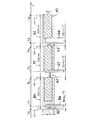
図8の実施例では、完全な秒パルス80,81,82が示されており、これらはそれぞれデータビット83〜85を揺する時間フレームを定めている。第1の秒パルス80は、時点t0で開始され、時点t2で終了する。この時点t2は同時に第2の秒パルス81の開始時点を形成しており、これは時点t4で終了している。第3の秒パルス82も第2の秒パルス81の終了時点t4で開始され、時点t6で終了している。
In the embodiment of FIG. 8, complete
一般に時点t0,t2,t4,t6は、各報時信号89の変わり目の開始を表わしている。それに対して時点t1,t3,5は、各報時信号89の変わり目の終了を表わしている。
In general, time points t0, t2, t4, and t6 indicate the start of the transition of each
各秒パルス80〜82の始まりにおいては、送信された信号は、例えばもとの振幅の25%まで低減された振幅を有する。第1の秒パルス80では、時点t0とt1の間の時間領域83において、送信された信号の低減された振幅が存在している。それに対して秒パルス80の時点t1とt2の間の残りの時間領域ではフルの振幅を有している。これらの低減された振幅の領域83〜85は、DCF−77のケースでは、T1=100msec若しくはT2=200msecである。その場合100msecのパルスは論理“0”の値に相応し、200msecのパルスは論理“1”の値に相応している。従って秒パルス80,82には、論理“0”が割当てられ、秒パルス81には論理“1”が割当てられる。ここでは逆の論理値あるいは別のパルス長も考えられる。
At the beginning of each second pulse 80-82, the transmitted signal has an amplitude reduced to, for example, 25% of the original amplitude. In the first
以下では本発明による方法を図8の概略的に示されている送信された報時信号と、図5〜図7のブロック回路図に示された装置に基づいて詳細に説明する。 In the following, the method according to the invention will be described in detail on the basis of the transmitted time signal shown schematically in FIG. 8 and the apparatus shown in the block circuit diagrams of FIGS.
論理/制御ユニット30は、正確にわかっている基準周波数に基づき、受信した所定の数の報時信号パルスに従って秒パルスの各開始に自動的に同期する。その場合秒開始への同期化に対しては内的若しくは外的な固定のタイムベースが用いられる。この固定のタイムベースの基本位置は、有利には各電子時計内に存在する水晶発振器の周波数であってもよい。これは正確に32.768kHzの周波数を供給している。それにより付加的な基準周波数は何も必要なくなる。この水晶時計の誤差及びその周波数から逓降された基準周波数の誤差は十分に満足のゆくレベルである。この基準周波数は、分周器を用いて、例えば分周値25=32でもって、良好な適用が可能な値まで、例えば1024Hzまで逓降される。
The logic /
TCOスタートパルスは、カウンタ52の計数状態55をリセットする。このカウンタ52は、装置44から生成された1024Hzの信号のパルスを連続的にカウントアップする。その場合各パルスはほぼ1msecの持続時間に相応する。ここにおいて新たなTCOパルス29がカウンタ52に供給されると、比較段53において、カウンタ状態55が比較段53の値“1000”よりも大きいのか、小さいのかそれとも等しいのかが決定される。カウンタ状態55がほぼこの値“1000”に相応するのならば、これは1秒(=1000msec)の間隔に相応し、新たな秒の開始としてマーキングされる。比較装置53は、その結果からパルス56を生成し、これは同期化パルスとして使用される。それと同時に同期化パルス57は、カウンタ52の計数状態55を0にリセットし、カウンタ52はここにおいて再び信号51によってクロック制御され、連続的にカウントアップされる。値“1000”の各新たな計数状態のもとでは、同期化パルス56があら他意にトリガされる。このようにして受信され増幅され整流された報時信号29の広範な領域に亘る高精度の同期化が内的なカウントシーケンス51によって実現される。
The TCO start pulse resets the counting
カウンタ52が計数状態1000に達する前に(ないしはそれに基づいて)TCOスタートパルス29が入力されると、同期化パルス56はトリガされない。このケースでは、計数状態55が再び0にリセットされるだけで新たにカウントアップが開始される。この過程は、入力側で再びスタートパルスが入力されるまで、すなわち計数状態55がほぼ値“1000”に相応するまで自動的に行われる。またここでは有利には、計数状態55が値“1000”から僅かだけずれている場合でも、これを同期化として解釈しそれに基づいて同期信号56を送出するようにしてもよい。
If the
このようにして、正確にわかっている基準周波数(32.768kHz信号)をベースにして論理/制御ユニット30は、受信した所定の数のスタートパルスに従って自動的に秒パルスの各開始に同期する。この場合この同期化は、送信された秒パルスの各パルス長には依存せずに行われる。この同期は、カウンタ52のいくつかの実行の後で及びいくつかの秒パルスの後で既に形成可能である。そのように形成された同期化のケースにおいては、秒パルスの正確な開始と各データビット83〜85の情報が正確にわかる。ここにおいてこれらのデータビット83〜85を読出すために、各秒パルス80〜82の全ての内容を読出す必要はない。それどころか相応するデータビット83〜85の終端を検査することで完全に十分である。なぜならばデータビット83〜85は異なる時報送信局から送信された報時信号に相応して任意の長さになるわけではなく、所定の長さを有するものなので、これらのデータパルス83〜85の各終端も正確にわかる。ドイツの標準時報局DCF−77から送信された信号のケースでは、各データビット83〜85の終端は、100msec後か若しくは200msec後に測定され、そこから秒パルス80〜82の開始が推定できる。このことは、これらの時間領域、すなわち100msec後と200msec後において、それらの振幅についての検査が必要となることを意味する。このことは次のように行われる。すなわち相応する持続時間の経過後に、さらに低減された振幅の存在に関する検出がなされるようにして行われる。その結果からデータビット83〜85のパルス持続時間と、データビット83〜85自体が推任される。このようにしてパルス83〜85へのビット値の即座の割当てが可能となる。
In this way, on the basis of a precisely known reference frequency (32.768 kHz signal), the logic /
二義的な曖昧性を回避するために、専ら正確な時点(秒パルス開始後の100msecないしは200msec後に生じる時点)のみを検査するのではなく、許容偏差の理由と障害の影響を避けるために、有利には、これらの時点の前後の所定の時間領域も加えることが可能である。それにより、許容偏差窓86〜88が100msecないし200msecの時間マーカーに生じる。これらの許容偏差窓86〜88は、そのつどの要求に適切に合わせることも可能である(例えば時間信号受信機が障害の多い領域内にあるのかどうかに関して)。例えば時間信号受信機が障害の多い領域内にあるならば、この許容偏差窓86〜88も十分広幅に選択される。
To avoid secondary ambiguity, instead of examining only the exact time points (time points that occur 100msec or 200msec after the start of the second pulse), in order to avoid the reason for tolerances and the effects of faults, Advantageously, it is also possible to add predetermined time zones before and after these time points. As a result,
これらの時間窓86〜88の設計仕様は、その上さらに基準周波数と同期化回路によって提供される受信感度にも向けられるべきである。 The design specifications for these time windows 86-88 should be further directed to the receiver frequency provided by the reference frequency and synchronization circuit.
有利な実施例では、100msecないし200msecの各領域のみが検査されのではなく、有利には、100msecの時点も200msecの時点も含んだ一貫した通しの時間窓86〜88がパルス振幅の上昇に基づいて検査される。例えば2つのケースにおいて秒開始後に75msec〜225msecの間の時間窓86〜88が用いられてもよい。上記例では、評価が各秒パルス80〜82内で150msecの期間の間だけ実施される。 In the preferred embodiment, only each region from 100 msec to 200 msec is not examined, and advantageously, a consistent series of time windows 86-88 that includes both 100 msec and 200 msec time points are based on pulse amplitude increases. Inspected. For example, in two cases, time windows 86-88 between 75 msec and 225 msec after the second start may be used. In the above example, the evaluation is performed only within a period of 150 msec within each second pulse 80-82.
それにより、時間窓86〜88の領域においてのみデータビットの評価が行われる。データビット83〜85の決定に係わる当該時間窓86〜88以外の領域は、本発明によれば考慮されることはなく、検査もされない。これにより、データビット83〜85の獲得のためのコストが最小限に抑えられる。それ故に受信され検査された報時信号における障害は当該領域においては無視できる。なぜならいずれにせよデータビット83〜85の確定には利用されないからである。
Thereby, the evaluation of the data bits is performed only in the region of the time windows 86-88. Areas other than the time windows 86-88 involved in determining the data bits 83-85 are not considered and are not examined according to the present invention. This minimizes the cost for acquiring data bits 83-85. Therefore, faults in the time signal received and examined are negligible in this area. This is because the
送信された報時信号からの正確な日付と正確な時間の本発明による復号化と出力は以下のように行われる。 The decoding and output according to the invention of the exact date and the exact time from the transmitted time signal is performed as follows.
報時テレグラムの最後のビットを用いれば自動的に次の報時テレグラムの完全な分のスタートパルスが識別できる。その場合識別されたデータビット83〜85の記憶が相応するシフトレジスタのデータテレグラムに割当てられた記憶箇所において行われる。データテレグラムの59のデータビット全てがシフトレジスタに記憶された後では、後置接続された評価ユニットにおいてデータが目下存在しピックアップ可能であることを知らせるために、出力信号71がセットされる。この評価ユニットは、電波時計のケースでは大抵は4ビットのマイクロコントローラで実現される。このマイクロコントローラは、ここにおいてこれらのデータを端子73を介して要求し、それに基づいてそれらのデータが端子49を介して速い順序でマイクロコントローラに伝送される。全データ伝送は、例えば分の全59ピットに対して例えば100msecだけ継続する。このマイクロコントローラはその後では再び他の目的に、例えば制御目的に自由に使えるようになる。この時間の間は、データ伝送に基づく障害によって生じ得る受信機の受信感度の影響を予防するために、受信回路の制御電圧がデータ伝送前に存在していた値に維持される。
Using the last bit of the time telegram, the complete start pulse of the next time telegram can be automatically identified. In that case, the storage of the identified
専用に設けられた制御線路の外部からの結線接続によって制御/論理ユニット30は、様々な送信プロトコルに設定調整できる。例えば論理/制御ユニット30と電波時計はドイツの送信プロトコルDCV77の他にもさらに付加的に若しくは代替的に他の送信プロトコル、例えばWWVB(USA),MSF(イギリス),JJY(日本),BPC(中国)の評価と後続処理が可能なように設計仕様することも可能である。
The control /
1つの時報送信局のプロトコルにおいて3以上のパルス長が存在するケースでは、有利な構成によれば、さらなるパルス長に、データテレグラム中の適切なビット値の位置の1つが割当てられる。それにより、1つの妥当性検査が可能となる。なぜなら時報送信局の様々なプロトコルが制御/論理装置30内に格納されているからである。非常に早期時点で、詳細にはマイクロコントローラがそのつどのデータをピックアップする前にエラー識別とその結果から導出されるエラー修正ルーチンないしエラー除去ルーチンが可能である。
In the case where there are more than two pulse lengths in a single time transmitting station protocol, according to an advantageous configuration, the further pulse length is assigned one of the appropriate bit value positions in the data telegram. Thereby, one validity check is possible. This is because various protocols of the time signal transmission station are stored in the control /
図9には、概略的に簡単に示した電波時計のブロック回路図が示されている。符号100で示されている電波時計は、時報送信局101から送信される報時信号3を受信するための1つ(又は複数の)アンテナ2を有している。このアンテナ2には、集積回路20(図6及び図7参照)が後置接続されている。この集積回路20は、論理/制御ユニット30(図6及び図7参照)を有している。アンテナ2と集積回路20は共に受信機1を形成する。この受信機の出力側にはプログラミング制御されたユニット102、例えばマイクロコントローラ若しくはマイクロプロセッサが後置接続されている。マイクロコントローラは、受信機によって生成されたデータビットを受入れ、そこから正確な時刻と正確な日付けを計算し、その結果から時刻と日付のための信号105を生成する。さらにこの電波時計100は、その時刻が水晶発信器104に基づいて制御される電子時計103を有している。この電子時計103は、表示部106、例えばディスプレイと接続されており、このディスプレイを介して時刻を表示する。ここにおいて電子時計103に信号105が供給されると、それに基づいて電子時計103は、表示している日付ないし時間を相応に修正する。
FIG. 9 shows a block circuit diagram of a radio-controlled timepiece schematically shown. The radio timepiece denoted by
本発明は、前述の有利な実施例に基づいて説明してきたが、これは本発明がこれらの実施例に限定されることを意味したものではない。それどころか多くの方式や形態の変更が可能である。 Although the invention has been described on the basis of the preferred embodiments described above, this does not mean that the invention is limited to these embodiments. On the contrary, many schemes and forms can be changed.
本発明は、必ずしも時報送信局DCF−77から送信された報時信号の受信のための受信機回路ないし電波時計に限定されるものではなく、本発明はもちろんその他の任意の時報送信局のもとでも有利に投入が可能である。 The present invention is not necessarily limited to a receiver circuit or a radio clock for receiving a time signal transmitted from a time signal transmission station DCF-77. Of course, the present invention is not limited to any other time signal transmission station. However, it can be advantageously introduced.
プログラム制御されたユニットに対しても必ずしもマイクロコントローラが必要というわけではない。それどころかこのマイクロコントローラの機能性は他の適切な回路、例えばマイクロプロセッサやデジタル信号プロセッサ(DSP)、ファジイコントローラ、固定的な配線若しくはプログラミング可能な論理回路、例えばFPGA回路、PLD回路などに置換えてもよい。 A microcontroller is not necessarily required for program-controlled units. On the contrary, the functionality of this microcontroller can be replaced by other suitable circuits such as microprocessors, digital signal processors (DSPs), fuzzy controllers, fixed wiring or programmable logic circuits such as FPGA circuits, PLD circuits, etc. Good.
特に本発明自体は、前述したような計数表示限定されるものではなく、これも単に例示的に示しただけのものである。本発明は当業者の技術知識の枠内で任意の変更が可能である。 In particular, the present invention itself is not limited to the counting display as described above, and this is also merely illustrative. The present invention can be arbitrarily modified within the scope of technical knowledge of those skilled in the art.
前述した具体的な回路技術的な変更も、可能性のあるいくつかの実施例を表わしただけのものであり、本発明による受信機の基本的な機能、特に同期化装置、時間発生器、記憶装置並びにそれに伴う本発明の対象からそれない限りは、簡単な構成素子や機能ユニットの交換による変更も非常に容易に可能である。 The specific circuit engineering changes described above are also only representative of some possible embodiments, and the basic functions of the receiver according to the invention, in particular the synchronization device, the time generator, As long as the storage device and the accompanying object of the present invention are not deviated from, the change by simply exchanging the constituent elements and functional units is very easy.
その上さらに本発明の電波時計の概念には、前述したような構造を有してはいるが、報時信号の伝送が有線で行われるもの、例えば通常の時計台装置などの電波時計も含まれる。 In addition, the concept of the radio timepiece of the present invention includes a radio timepiece such as a normal clock tower device, which has a structure as described above, but transmits a time signal in a wired manner. It is.
前述した実施例では、コード化がそれぞれ搬送波信号の時間フレーム開始時の低減によって実現されていたが、このコード化自体ももちろん振幅の上昇によって実現されてもよいし、一般的な搬送波信号の振幅の変化によって実現されてもよい。同様に、前述の実施例においては報時信号振幅の変化の開始が検出されていた。本発明によればこの開始に基づいてそれぞれの終端もそのつどのコード化に依存して推定されていた。これらのことも単に例示していただけのものであって、同じような形態で終端の検出に基づいて開始を推定することももちろん可能である。このケースでは、本発明の基本的な原理から逸脱することなく搬送波信号振幅の変化の開始時点が逆算され得る。さらに同じような形態で本発明による方法によれば有利には、変更の開始が確定されると、それに基づいて検査すべき終端に対する時間領域が確定され得るが、その逆のケースにおいても回路技術的に僅かな付加的コスト、例えば1つのバッファメモリを要するだけで終端からの逆算が可能となる。 In the above-described embodiments, the encoding is realized by reducing the carrier signal at the start of the time frame. However, the encoding itself may of course be realized by increasing the amplitude, or the amplitude of a general carrier signal. It may be realized by the change of. Similarly, in the above-described embodiment, the start of the change of the time signal amplitude is detected. According to the invention, on the basis of this start, each end is also estimated depending on the respective coding. These are also merely illustrative, and it is of course possible to estimate the start based on end detection in a similar manner. In this case, the starting point of the change in carrier signal amplitude can be calculated back without departing from the basic principle of the present invention. Furthermore, according to the method according to the invention in a similar manner, once the start of the change has been determined, the time domain for the end to be examined can be determined on the basis of it, and vice versa. Therefore, it is possible to perform back calculation from the end with only a small additional cost, for example, only one buffer memory is required.
1 受信機、受信回路
2 (フェライト)アンテナ
3 報時信号
4 制御増幅器、入力側増幅器
5 制御信号、制御電圧
6 (圧電)フィルタ、コンデンサ
7 後段増幅器
8 整流器
9 減算器
10 整流され増幅された信号
11 基準信号
12 基準源
13 メモリコンデンサ
14 復号化装置
15 受信機出力側
20 集積回路
21,22 入力側、アンテナ入力側
21′,22′ 入力側、基準入力側
23,24 制御可能スイッチ
25 スイッチユニット、切換え可能フィルタ
26 制御入力側
27,28 制御信号
29 整流され増幅された報時信号
30 論理制御ユニット
31 制御信号
32 入/出力装置,I/Oユニット
33 出力側
34,35 給電電位のための端子
36,37 制御端子
38 制御信号
40 報時信号入力側
41 クロック制御信号入力側
42 クロック制御信号
43 同期化ユニット
44 時間ベース生成装置、基準化装置
45 時間発生器(ビット識別回路)
46 ビット識別制御部(ビット識別回路)
47 メモリ装置
48 出力インターフェース,出力シフトレジスタ
49 論理制御ユニットのデータ出力側
51 分周されたクロック信号(固定タイムベース)
52 カウンタ
53 比較装置,比較器
54 制御装置、リセットユニット
55 計数状態、計数状態信号
56 同期信号
57,58 リセット信号
60 出力側
61−65 記憶装置
66 制御信号
67 比較装置
68 制御信号
69 決定装置
70 ビットメモリスペース
72 出力側
73 (要求)入力側
80−82 秒パルス,(時間)フレーム
83−85 データバス,減少された振幅を有するパルス
86−88 時間窓
89 報時信号
100 電波時計
101 報時送信局
102 プログラム制御されたユニット,マイクロコントローラ,マイクロプロセッサ
103 電子時計、自動時計
104 水晶時計
105 正確な時刻/日付のための信号
106 表示部
t0−t6 時点
T1,T2 持続時間
T3 フレーム期間
VCC (正の)給電電圧
GND 基準電位
IN1,IN2 基準信号
QL,QM,QIN,QH 制御信号
SS1,SS2 制御信号
A 符号化概要図
B 一般的符号化ビット
C 一般的日付/時刻情報
D “分”ビット
E “時”ビット
F “日”ビット
G “曜日”ビット
H “月”ビット
I “年”ビット
M “分”マーカー
R “アンテナビット
A1 MEZからMESZへの伝送のための予告ビット
Z1,Z2 ゾーン時間ビット
A2 閏秒に対する予告ビット
S 符号化された時間情報のスタートビット
P1,P2,P3 検査ビット
X (報時)搬送波信号
X1,X2 搬送波信号の立ち下がり
DESCRIPTION OF
46 bit identification control unit (bit identification circuit)
47
52 Counter 53 Comparison Device, Comparator 54 Control Device, Reset Unit 55 Counting State, Counting State Signal 56 Synchronization Signal 57, 58 Reset Signal 60 Output Side 61-65 Storage Device 66 Control Signal 67 Comparison Device 68 Control Signal 69 Determination Device 70 Bit memory space 72 Output side 73 (Request) Input side 80-82 second pulse, (Time) frame 83-85 Data bus, Pulse with reduced amplitude 86-88 Time window 89 Time signal 100 Time signal 101 Time signal Transmitting station 102 Program-controlled unit, microcontroller, microprocessor 103 Electronic clock, automatic clock 104 Quartz clock 105 Signal for accurate time / date 106 Display section t0-t6 Time point T1, T2 Duration T3 Frame period VCC ( Positive) supply voltage GN D Reference potential IN1, IN2 Reference signal QL, QM, QIN, QH Control signal SS1, SS2 Control signal A Encoding overview diagram B General encoding bit C General date / time information D “Minute” bit E “Hour” bit F “Day” bit G “Day of the week” bit H “Month” bit I “Year” bit M “Minute” marker R “Antenna bit A1 Notice bit for transmission from MEZ to MESZ Z1, Z2 Zone time bit A2 Leap second Predictive bit for S S Start bit of encoded time information P1, P2, P3 Check bit X (Information) Carrier signal X1, X2 Falling of carrier signal
Claims (13)
報時信号(89)が一定の持続時間の多数の時間フレーム(80〜82)から成っている形式の方法において、
時間情報の獲得のために、時間フレーム毎に、1つの時間フレーム(80〜82)の持続時間よりも短い少なくとも1つの時間領域(86,87,88)をそれぞれ報時信号(89)の振幅の変化に基づいて検査するようにし、さらに、
前記報時信号(89)内の時間情報は、ビット形態で存在し、その場合それぞれ1つの時間フレーム(80〜82)に少なくとも1つのデータビット(83〜85)が割当てられ、当該データビット(83〜85)の値は、報時信号(89)の振幅変化の持続時間(T1,T2)によって定められ、報時信号(89)の振幅変化の第1の持続時間(T1)は、データビット(83,85)の第1の論理値に相応し、振幅変化の第2の持続時間(T2)は、データビット(84)の第2の論理値に相応し、さらに、
振幅変化の第1の時点(t0,t2,t4)を確定し、
振幅変化の第1の時点(t0,t2,t4)並びに第1及び第2の持続時間(T1,T2)から、第1の持続時間(T1)に関する第2の時点(t1,t5)と第2の持続時間(T2)に関する第3の時点(t3)を定め、
第1の時点(t1,t5)近傍に設けられている第1の時間領域(86)は、報時信号(89)の振幅が当該振幅の最初の値をとっているかどうかについて検査され、
第1の領域(86)における振幅が最初の値をとっている場合には、データビット(83)に第1の論理値が割当てられるようにしたことを特徴とする方法。 A method for acquiring time information from a time signal (89) transmitted from a time signal transmitting station (101),
In a method of the type in which the time signal (89) consists of a number of time frames (80-82) of constant duration,
In order to acquire time information, for each time frame, at least one time region (86, 87, 88) that is shorter than the duration of one time frame (80 to 82) is used for the amplitude of the time signal (89). Based on changes in the
The time information in the time signal (89) exists in the form of bits, in which case at least one data bit (83 to 85) is assigned to each time frame (80 to 82), and the data bit ( 83 to 85) is determined by the duration (T1, T2) of the amplitude change of the time signal (89), and the first duration (T1) of the amplitude change of the time signal (89) is the data corresponds to a first logic value of the bit (83, 85), a second duration of amplitude change (T2) is to correspond to a second logic value of the data bits (84), further,
Confirm the first time point (t0, t2, t4) of the amplitude change;
From the first time point (t0, t2, t4) of the amplitude change and the first and second durations (T1, T2), the second time point (t1, t5) and the first time for the first duration (T1). A third time point (t3) for a duration of 2 (T2),
The first time region (86) provided in the vicinity of the first time point (t1, t5) is inspected as to whether the amplitude of the time signal (89) takes the first value of the amplitude,
A method wherein a first logical value is assigned to a data bit (83) when the amplitude in the first region (86) takes an initial value .
報時信号(89)が一定の持続時間の多数の時間フレーム(80〜82)から成っており、
報時信号(89)内の時間情報は、ビット形態で存在し、その場合それぞれ1つの時間フレーム(80〜82)に少なくとも1つのデータビット(83〜85)が割当てられ、
当該データビット(83〜85)の値は、報時信号(89)の振幅変化の持続時間(T1,T2)によって定められ、
報時信号(89)の振幅変化の第1の持続時間(T1)は、データビット(83,85)の第1の論理値に相応し、
振幅変化の第2の持続時間(T2)は、データビット(84)の第2の論理値に相応する形式の方法において、
振幅変化の第1の時点(t0,t2,t4)を確定し、
振幅変化の第1の時点(t0,t2,t4)並びに第1及び第2の持続時間(T1,T2)から、第1の持続時間(T1)に関する第2の時点(t1,t5)と第2の持続時間(T2)に関する第3の時点(t3)を定め、
第1の時点(t1,t5)近傍に設けられている第1の時間領域(86)は、報時信号(89)の振幅が当該振幅の最初の値をとっているかどうかについて検査され、
第1の領域(86)における振幅が最初の値をとっている場合には、データビット(83)に第1の論理値が割当てられるようにしたことを特徴とする方法。 A method for acquiring time information from a time signal (89) transmitted from a time signal transmitting station (101),
The time signal (89) consists of a number of time frames (80-82) of constant duration,
The time information in the time signal (89) exists in the form of bits, in which case at least one data bit (83-85) is assigned to each time frame (80-82),
The value of the data bits (83 to 85) is determined by the duration (T1, T2) of the amplitude change of the time signal (89),
The first duration (T1) of the amplitude change of the time signal (89) corresponds to the first logical value of the data bits (83, 85),
The second duration of amplitude change (T2) is a method of the type corresponding to the second logical value of the data bits (84),
Confirm the first time point (t0, t2, t4) of the amplitude change;
From the first time point (t0, t2, t4) of the amplitude change and the first and second durations (T1, T2), the second time point (t1, t5) and the first time for the first duration (T1). A third time point (t3) for a duration of 2 (T2),
The first time region (86) provided in the vicinity of the first time point (t1, t5) is inspected as to whether the amplitude of the time signal (89) takes the first value of the amplitude,
A method wherein a first logical value is assigned to a data bit (83) when the amplitude in the first region (86) takes an initial value.
59ないし60の全てのデータビットが中間メモリ(70)から読出されてバッファメモリ(48)に供給され、
前記供給されたデータビットは、特にシリアルに、計算ユニットへ伝送され、
計算ユニットは、読出された59ないし60のデータビットから正確な時間および/または正確な日付を算出する、請求項1から8いずれか1項記載の方法。 Starting from the first data bit of the data telegram, 59 to 60 data bits are successively stored in succession,
All data bits 59 to 60 are read from the intermediate memory (70) and supplied to the buffer memory (48),
The supplied data bits are transmitted to the computing unit, in particular serially,
Calculation unit, read-out 59 to not calculate the exact time and / or precise date from 60 data bits, the method according to any one of claims 1 8.
前記受信装置は、
前記報時信号(3)を受け取るための少なくとも1つのアンテナ(2)と、
前記報時信号(3)内に含まれる時間情報を取り出すための論理/制御ユニット(30)と、
前記論理/制御ユニット(30)の出力側に接続された入/出力ユニット(32)とを有し、該入/出力ユニット(32)の出力側からは、前記報時信号(3)から取り出した時間情報から導出された出力信号を送出するように構成されている、受信装置(1)において、
前記論理/制御ユニット(30)がビット識別回路(45,46)を含んでおり、該ビット識別回路(45,46)は、報時テレグラムのプロトコルと振幅変化の持続時間に相応してデータビットに第1の論理値若しくは第2の論理値を割当てるように構成されており、さらに、
前記ビット識別回路(45,46)は、時間発生器(45)を含んでおり、該時間発生器(45)は、固定タイムベース(51)に基づき報時テレグラムのプロトコルに応じて、振幅変化の持続時間が、論理"0"に相応する第1の持続時間(T1)に相応しているのか、又は論理"1"に相応する第2の持続時間(T2)に相応しているのか、を確定するように構成されていることを特徴とする受信装置。 By using the method according to claims 1 9, a receiving apparatus for receiving a time signal containing time information between (3) (1),
The receiving device is :
At least one antenna (2) for receiving said time signal (3);
A logic / control unit (30) for extracting time information contained in the report time signal (3) in,
Said logic / control and a unit (30) connected to input / output unit to the output side of (32), from the output side of the input / output unit (32), taken from the report time signal (3) and it is configured to deliver output to the output signal derived from the time information in the receiving device (1),
The logic / control unit (30) includes a bit identification circuit (45, 46), the bit identification circuit (45, 46) corresponding to the protocol of the time telegram and the duration of the amplitude change. Is assigned a first logical value or a second logical value, and
The bit identification circuit (45, 46) includes a time generator (45), and the time generator (45) changes amplitude according to a protocol of a time telegram based on a fixed time base (51). Is corresponding to a first duration (T1) corresponding to a logic "0" or to a second duration (T2) corresponding to a logic "1", A receiving apparatus configured to determine
前記カウンタ(52)は、基準周波数による制御によってその計数状態(52)をカウントアップしており、
前記比較器(53)は、カウンタ(52)の計数状態(55)を所定の値、特に時間フレームの持続時間(T3)に相応する値と比較し、
前記リセットユニット(54)は、計数状態(55)と所定の値とが一致した場合に、若しくは新たな報時信号(29)が現れた場合に、前記カウンタ(52)をリセットし、
前記出力ユニット(53)は、カウンタ(52)の計数状態(55)が所定の値と一致した場合に、ビット識別回路(45,46)の駆動制御のための同期信号(56)を発生する、請求項11記載の受信装置。 The synchronization device (43) includes a counter (52), a comparator (53), a reset unit (54), and an output unit (53).
The counter (52) counts up its counting state (52) by control with a reference frequency,
The comparator (53) compares the counting state (55) of the counter (52) with a predetermined value, in particular a value corresponding to the duration (T3) of the time frame,
The reset unit (54) resets the counter (52) when the counting state (55) matches a predetermined value or when a new time signal (29) appears,
The output unit (53) generates a synchronization signal (56) for driving control of the bit identification circuit (45, 46) when the count state (55) of the counter (52) matches a predetermined value. The receiving device according to claim 11 .
Applications Claiming Priority (2)
| Application Number | Priority Date | Filing Date | Title |
|---|---|---|---|
| DE10334990.1A DE10334990B4 (en) | 2003-07-31 | 2003-07-31 | Radio Clock |
| DE10334990.1 | 2003-07-31 |
Publications (3)
| Publication Number | Publication Date |
|---|---|
| JP2005055439A JP2005055439A (en) | 2005-03-03 |
| JP2005055439A5 JP2005055439A5 (en) | 2007-09-13 |
| JP4868488B2 true JP4868488B2 (en) | 2012-02-01 |
Family
ID=33521502
Family Applications (1)
| Application Number | Title | Priority Date | Filing Date |
|---|---|---|---|
| JP2004224662A Active JP4868488B2 (en) | 2003-07-31 | 2004-07-30 | Radio clock |
Country Status (5)
| Country | Link |
|---|---|
| US (1) | US7486657B2 (en) |
| EP (1) | EP1503257A3 (en) |
| JP (1) | JP4868488B2 (en) |
| CN (1) | CN100552571C (en) |
| DE (1) | DE10334990B4 (en) |
Families Citing this family (13)
| Publication number | Priority date | Publication date | Assignee | Title |
|---|---|---|---|---|
| DE10357201A1 (en) * | 2003-12-08 | 2005-07-07 | Atmel Germany Gmbh | Radio Clock |
| US7333467B2 (en) * | 2003-12-08 | 2008-02-19 | Atmel Germany Gmbh | Receiver circuit and method using selectively variable amplification for receiving time signals from different transmitters |
| DE102004004416A1 (en) * | 2004-01-29 | 2005-08-18 | Atmel Germany Gmbh | Method for determining the signal quality of a transmitted time signal |
| DE102004004411B4 (en) * | 2004-01-29 | 2015-08-20 | Atmel Corp. | Radio clock and method for obtaining time information |
| DE102004004375B4 (en) * | 2004-01-29 | 2019-08-08 | Atmel Corp. | Method for obtaining time information and radio clock |
| DE102004005340A1 (en) * | 2004-02-04 | 2005-09-01 | Atmel Germany Gmbh | Method for obtaining time information, receiver circuit and radio clock |
| DE102006060924B3 (en) | 2006-12-20 | 2008-06-19 | Atmel Germany Gmbh | Wireless programming method for time signal receiver, involves transmitting programming instruction, which is coded in adapted data format on time signal receiver, of transmitting device |
| DE102006060927A1 (en) * | 2006-12-20 | 2008-06-26 | Atmel Germany Gmbh | Signaling device for household appliance, particularly smoke detector, has time signal receiver which has receiving unit that receives electromagnetic time signal and processing unit for processing time signal |
| JP5386786B2 (en) * | 2007-03-26 | 2014-01-15 | カシオ計算機株式会社 | Time information receiver and radio clock |
| CN103222225A (en) | 2010-09-22 | 2013-07-24 | Dba扩展波有限责任公司 | Low power radio controlled clock incorporating independent timing corrections |
| US8270465B1 (en) | 2011-11-15 | 2012-09-18 | Xw Llc | Timing and time information extraction from a phase modulated signal in a radio controlled clock receiver |
| US8693582B2 (en) | 2012-03-05 | 2014-04-08 | Xw Llc | Multi-antenna receiver in a radio controlled clock |
| JP6387860B2 (en) * | 2015-03-04 | 2018-09-12 | セイコーエプソン株式会社 | Radio clock and radio clock control method |
Family Cites Families (58)
| Publication number | Priority date | Publication date | Assignee | Title |
|---|---|---|---|---|
| CH496278A (en) | 1967-11-01 | 1970-05-29 | Suisse De Rech S Horlogeres La | Installation for detecting an identification signal in a time signal transmission |
| DE2643250B2 (en) | 1976-09-25 | 1978-07-27 | Braun Ag, 6000 Frankfurt | Centrally controlled clock |
| DE2802040A1 (en) | 1978-01-16 | 1979-07-19 | Peter Gravenhorst | Digital clock system using transmitted time signals - includes internal correction for transmission errors using microcomputer between buffer register store and display |
| US4287597A (en) * | 1978-09-05 | 1981-09-01 | Arbiter Systems Incorporated | Satellite controlled clock |
| DE3015312A1 (en) | 1980-04-21 | 1981-10-22 | Wolfgang Dr.-Ing. 6101 Groß-Bieberau Hilberg | Display of signal quality received by radio controlled clock - compares second timing impulses with reference level to drive visual indicator |
| DE3022949C2 (en) * | 1980-06-19 | 1983-11-17 | Werner 6802 Ladenburg Schulz | Process for the automatic correction of the rate deviation of a clock |
| DE3101406A1 (en) | 1981-01-17 | 1983-01-05 | Wolfgang Dr.-Ing. 6101 Groß-Bieberau Hilberg | Automatic radio clock adjustment |
| DE3236162A1 (en) | 1982-09-30 | 1984-04-05 | Rainer Dipl.-Ing. 6500 Mainz Bermbach | Self-tuning narrow-band receiver |
| DE3346091A1 (en) | 1982-09-30 | 1985-07-04 | Rainer Dipl.-Ing. 6500 Mainz Bermbach | Self-adjusting narrowband receiver |
| DE3504338A1 (en) | 1985-02-08 | 1986-08-14 | Rainer Dipl.-Ing. 6500 Mainz Bermbach | Frequency adjustment in radio clocks |
| DE3516810A1 (en) | 1985-05-10 | 1986-11-13 | Junghans Uhren GmbH, 7230 Schramberg | RECEIVER FOR AMPLITUDE SWITCHED TIMING SIGNALS |
| US4768178A (en) * | 1987-02-24 | 1988-08-30 | Precision Standard Time, Inc. | High precision radio signal controlled continuously updated digital clock |
| DE3719650A1 (en) | 1987-06-12 | 1988-12-22 | Forschungsgesellschaft Fuer Fe | Controller for radio time signal receiver |
| US4823328A (en) * | 1987-08-27 | 1989-04-18 | Conklin Charles C | Radio signal controlled digital clock |
| DE3733966A1 (en) * | 1987-10-08 | 1989-04-20 | Ulrich Dipl Ing Bellmann | Arrangement for receiving severely disturbed signals of the transmitter DCF-77 |
| DE3733965A1 (en) | 1987-10-08 | 1989-04-20 | Ulrich Dipl Ing Bellmann | Method for obtaining information from strongly mutilated data of a time signal transmitter |
| DE9010270U1 (en) | 1990-05-04 | 1991-09-05 | Junghans Uhren Gmbh, 7230 Schramberg, De | |
| JPH04105092A (en) * | 1990-08-24 | 1992-04-07 | Nec Eng Ltd | Clock dial synchronous system |
| JPH07109434B2 (en) | 1991-11-19 | 1995-11-22 | 株式会社精工舎 | clock |
| JP2555502B2 (en) | 1992-02-19 | 1996-11-20 | 株式会社精工舎 | Radio-corrected clock and its reception time setting method and time correction method |
| JP2503376B2 (en) | 1992-06-18 | 1996-06-05 | 株式会社精工舎 | Radio wave correction clock |
| DE4227502C2 (en) | 1992-08-20 | 1995-11-02 | Smi Syst Microelect Innovat | Receiver for amplitude-sampled time signal signals |
| DE4233126A1 (en) | 1992-10-02 | 1994-04-07 | Telefunken Microelectron | Procedure for the operation of a radio clock and radio clock for use in an environment subject to interference |
| DE4242384C2 (en) | 1992-12-08 | 1996-08-14 | Smi Syst Microelect Innovat | Receiver for amplitude-sampled time signal signals |
| DE9300945U1 (en) * | 1993-01-25 | 1994-05-26 | Junghans Uhren Gmbh | Autonomous radio clock |
| DE4332798A1 (en) | 1993-09-27 | 1995-03-30 | Telefunken Microelectron | Circuit arrangement for a tunable resonant circuit |
| DE4403124C2 (en) | 1994-02-02 | 1997-02-13 | Telefunken Microelectron | Method for operating a radio clock |
| DE4412892A1 (en) | 1994-04-14 | 1995-10-26 | Fritz Schaeffel | Autonomous radio watch or clock with radio receiver and aerial |
| DE4427885A1 (en) * | 1994-08-08 | 1996-02-15 | Telefunken Microelectron | Noise-reduced data reconstruction method for data transmission system |
| DE4442818A1 (en) | 1994-12-01 | 1996-06-05 | Afg Elektronik Gmbh | AM digital signal receiver, esp. for time-signal transmissions or radio clock |
| DE19514030C2 (en) | 1995-04-13 | 1998-09-17 | Telefunken Microelectron | Method for recognizing the time telegrams in the disturbed signal of a time signal transmitter |
| DE19514036C2 (en) | 1995-04-13 | 1997-08-21 | Telefunken Microelectron | Method for determining the start of seconds in the signal of a time signal transmitter |
| DE19514031C2 (en) | 1995-04-13 | 1997-07-10 | Telefunken Microelectron | Method for detecting the beginning of time frames |
| DE19522621B4 (en) * | 1995-06-22 | 2004-01-15 | Atmel Germany Gmbh | Method for decoding transmitted information units |
| DE19540592A1 (en) | 1995-10-31 | 1997-05-15 | Braun Ag | Radio clock with reception quality display |
| JPH1130677A (en) | 1997-07-10 | 1999-02-02 | Sony Corp | Time data processing circuit |
| DE19808431A1 (en) | 1998-03-02 | 1999-09-09 | Junghans Uhren Gmbh | Multi-channel radio clock for use in different geographical locations |
| DE29813498U1 (en) | 1998-07-29 | 1999-12-09 | H & S Hard & Software Technolo | Time signal synchronization device |
| DE29914606U1 (en) | 1999-08-20 | 2000-12-28 | Diehl Stiftung & Co | Radio reception tester |
| US7102964B2 (en) * | 2000-02-10 | 2006-09-05 | Seiko Epson Corporation | Time keeping apparatus and control method therefor |
| JP3596464B2 (en) * | 2000-02-10 | 2004-12-02 | セイコーエプソン株式会社 | Timing device and control method of timing device |
| US6359525B1 (en) * | 2000-07-25 | 2002-03-19 | Thomson Licensing S.A. | Modulation technique for transmitting multiple high data rate signals through a band limited channel |
| JP2002048881A (en) * | 2000-07-31 | 2002-02-15 | Rhythm Watch Co Ltd | Composite device and method for standard wave |
| JP2002286877A (en) | 2001-03-28 | 2002-10-03 | Seiko Clock Inc | Method and apparatus of deciding start timing of time frame, time information detector and radio-controlled clock |
| JP2003125012A (en) | 2001-10-16 | 2003-04-25 | Matsushita Electric Ind Co Ltd | Ask demodulator with agc |
| JP4233311B2 (en) * | 2001-11-20 | 2009-03-04 | シチズンホールディングス株式会社 | Radio clock, standard radio wave reception method and electronic equipment |
| JP2003167073A (en) * | 2001-11-29 | 2003-06-13 | Seiko Instruments Inc | Radio wave correcting device and radio wave correcting clock using it |
| HK1050114A2 (en) * | 2002-04-04 | 2003-05-16 | Idt Lcd Holding Bvi Ltd | Radio control clock |
| ATE324703T1 (en) | 2002-10-16 | 2006-05-15 | Casio Computer Co Ltd | RADIO WAVE RECEIVING DEVICE, RADIO WAVE CLOCK, AND REPEATER |
| JP2006505990A (en) * | 2002-11-07 | 2006-02-16 | コーニンクレッカ フィリップス エレクトロニクス エヌ ヴィ | Mobile radio receiver with improved real-time accuracy |
| CN1627213A (en) * | 2003-11-28 | 2005-06-15 | Atmel德国有限公司 | Radio-controlled clock and method for acquiring time information from a time signal |
| US7333467B2 (en) * | 2003-12-08 | 2008-02-19 | Atmel Germany Gmbh | Receiver circuit and method using selectively variable amplification for receiving time signals from different transmitters |
| DE10357201A1 (en) * | 2003-12-08 | 2005-07-07 | Atmel Germany Gmbh | Radio Clock |
| DE10361593A1 (en) * | 2003-12-30 | 2005-07-28 | Atmel Germany Gmbh | Method for determining the start of seconds from a transmitted time signal |
| DE102004004411B4 (en) * | 2004-01-29 | 2015-08-20 | Atmel Corp. | Radio clock and method for obtaining time information |
| DE102004004416A1 (en) * | 2004-01-29 | 2005-08-18 | Atmel Germany Gmbh | Method for determining the signal quality of a transmitted time signal |
| DE102004004375B4 (en) * | 2004-01-29 | 2019-08-08 | Atmel Corp. | Method for obtaining time information and radio clock |
| DE102004005340A1 (en) * | 2004-02-04 | 2005-09-01 | Atmel Germany Gmbh | Method for obtaining time information, receiver circuit and radio clock |
-
2003
- 2003-07-31 DE DE10334990.1A patent/DE10334990B4/en not_active Expired - Lifetime
-
2004
- 2004-07-29 EP EP04017915A patent/EP1503257A3/en not_active Withdrawn
- 2004-07-30 JP JP2004224662A patent/JP4868488B2/en active Active
- 2004-08-02 CN CNB2004100557238A patent/CN100552571C/en active Active
- 2004-08-02 US US10/910,261 patent/US7486657B2/en active Active
Also Published As
| Publication number | Publication date |
|---|---|
| US7486657B2 (en) | 2009-02-03 |
| CN1580982A (en) | 2005-02-16 |
| CN100552571C (en) | 2009-10-21 |
| DE10334990A1 (en) | 2005-03-24 |
| DE10334990B4 (en) | 2016-03-17 |
| EP1503257A3 (en) | 2008-01-30 |
| EP1503257A2 (en) | 2005-02-02 |
| JP2005055439A (en) | 2005-03-03 |
| US20050036514A1 (en) | 2005-02-17 |
Similar Documents
| Publication | Publication Date | Title |
|---|---|---|
| JP4868488B2 (en) | Radio clock | |
| CN101571701B (en) | Radio-controlled timepiece and control method for a radio-controlled timepiece | |
| JP2005221505A (en) | Method of acquiring clock information from received time code signal having modulated amplitude, radio-controlled clock for executing the method, and receiver circuit for radio-controlled clock | |
| JP2005214979A (en) | Method of obtaining signal quality from time code signal, and receiver circuit | |
| US7317905B2 (en) | Radio-controlled clock and method for gaining time information | |
| JP4768278B2 (en) | Method for obtaining time information from time code signal and radio clock or receiver circuit for radio clock for implementing the method | |
| JP4322786B2 (en) | Multiple standard radio wave decoding method and standard radio wave receiver | |
| JP2005195597A (en) | Method for determining beginning of second from transmitted time signal including time information | |
| JP3796380B2 (en) | Time correction information output device and automatic time correction clock | |
| US20050122952A1 (en) | Radio-controlled clock and method for automatically receiving and evaluating any one of plural available time signals | |
| US20150268637A1 (en) | Radio timepiece and receipt control method | |
| US20050116856A1 (en) | Radio-controlled clock and method for acquiring time information from a time signal with reduced evaluation overhead | |
| US9709961B2 (en) | Radio controlled timepiece and method for controlling radio controlled timepiece | |
| JP2010175328A (en) | Radio-controlled timepiece and control method for the same | |
| JP5083384B2 (en) | Time data receiver and radio clock | |
| JP2003215277A (en) | Standard-wave decoding circuit and marker detection circuit as well as radio-controlled timepiece | |
| JP2011226813A (en) | Gps time piece and its method | |
| JP5309571B2 (en) | Radio correction watch and control method thereof | |
| JP4255307B2 (en) | Time data supply apparatus and time data supply method | |
| US20050213433A1 (en) | Localized signal radio adjusted clock | |
| JP2013007684A (en) | Time accuracy measuring apparatus and method | |
| JP4483226B2 (en) | Time information transmitting / receiving device and wristwatch | |
| KR820000433B1 (en) | Electric clock having automatically-time adjusting means | |
| US20090003140A1 (en) | Method for wireless programming of a time signal receiver, wirelessly programmable time signal receiver, and programming device for wireless programming of a time signal receiver | |
| Series | Protection criteria for systems in the standard frequency and time signal services |
Legal Events
| Date | Code | Title | Description |
|---|---|---|---|
| A521 | Request for written amendment filed |
Free format text: JAPANESE INTERMEDIATE CODE: A523 Effective date: 20070730 |
|
| A621 | Written request for application examination |
Free format text: JAPANESE INTERMEDIATE CODE: A621 Effective date: 20070730 |
|
| A977 | Report on retrieval |
Free format text: JAPANESE INTERMEDIATE CODE: A971007 Effective date: 20101020 |
|
| A131 | Notification of reasons for refusal |
Free format text: JAPANESE INTERMEDIATE CODE: A131 Effective date: 20101029 |
|
| RD04 | Notification of resignation of power of attorney |
Free format text: JAPANESE INTERMEDIATE CODE: A7424 Effective date: 20101228 |
|
| A601 | Written request for extension of time |
Free format text: JAPANESE INTERMEDIATE CODE: A601 Effective date: 20110126 |
|
| A602 | Written permission of extension of time |
Free format text: JAPANESE INTERMEDIATE CODE: A602 Effective date: 20110202 |
|
| A601 | Written request for extension of time |
Free format text: JAPANESE INTERMEDIATE CODE: A601 Effective date: 20110225 |
|
| A602 | Written permission of extension of time |
Free format text: JAPANESE INTERMEDIATE CODE: A602 Effective date: 20110302 |
|
| A521 | Request for written amendment filed |
Free format text: JAPANESE INTERMEDIATE CODE: A523 Effective date: 20110427 |
|
| A131 | Notification of reasons for refusal |
Free format text: JAPANESE INTERMEDIATE CODE: A131 Effective date: 20110602 |
|
| A601 | Written request for extension of time |
Free format text: JAPANESE INTERMEDIATE CODE: A601 Effective date: 20110901 |
|
| A602 | Written permission of extension of time |
Free format text: JAPANESE INTERMEDIATE CODE: A602 Effective date: 20110906 |
|
| A521 | Request for written amendment filed |
Free format text: JAPANESE INTERMEDIATE CODE: A523 Effective date: 20111003 |
|
| TRDD | Decision of grant or rejection written | ||
| A01 | Written decision to grant a patent or to grant a registration (utility model) |
Free format text: JAPANESE INTERMEDIATE CODE: A01 Effective date: 20111027 |
|
| A01 | Written decision to grant a patent or to grant a registration (utility model) |
Free format text: JAPANESE INTERMEDIATE CODE: A01 |
|
| A61 | First payment of annual fees (during grant procedure) |
Free format text: JAPANESE INTERMEDIATE CODE: A61 Effective date: 20111111 |
|
| R150 | Certificate of patent or registration of utility model |
Ref document number: 4868488 Country of ref document: JP Free format text: JAPANESE INTERMEDIATE CODE: R150 Free format text: JAPANESE INTERMEDIATE CODE: R150 |
|
| FPAY | Renewal fee payment (event date is renewal date of database) |
Free format text: PAYMENT UNTIL: 20141125 Year of fee payment: 3 |
|
| R250 | Receipt of annual fees |
Free format text: JAPANESE INTERMEDIATE CODE: R250 |
|
| R250 | Receipt of annual fees |
Free format text: JAPANESE INTERMEDIATE CODE: R250 |
|
| R250 | Receipt of annual fees |
Free format text: JAPANESE INTERMEDIATE CODE: R250 |
|
| R250 | Receipt of annual fees |
Free format text: JAPANESE INTERMEDIATE CODE: R250 |
|
| R250 | Receipt of annual fees |
Free format text: JAPANESE INTERMEDIATE CODE: R250 |
|
| R250 | Receipt of annual fees |
Free format text: JAPANESE INTERMEDIATE CODE: R250 |
|
| R250 | Receipt of annual fees |
Free format text: JAPANESE INTERMEDIATE CODE: R250 |
|
| R250 | Receipt of annual fees |
Free format text: JAPANESE INTERMEDIATE CODE: R250 |
|
| R250 | Receipt of annual fees |
Free format text: JAPANESE INTERMEDIATE CODE: R250 |
|
| R250 | Receipt of annual fees |
Free format text: JAPANESE INTERMEDIATE CODE: R250 |