JP4862760B2 - Detection signal processing circuit - Google Patents
Detection signal processing circuit Download PDFInfo
- Publication number
- JP4862760B2 JP4862760B2 JP2007165121A JP2007165121A JP4862760B2 JP 4862760 B2 JP4862760 B2 JP 4862760B2 JP 2007165121 A JP2007165121 A JP 2007165121A JP 2007165121 A JP2007165121 A JP 2007165121A JP 4862760 B2 JP4862760 B2 JP 4862760B2
- Authority
- JP
- Japan
- Prior art keywords
- detection signal
- circuit
- detection
- level
- signal
- Prior art date
- Legal status (The legal status is an assumption and is not a legal conclusion. Google has not performed a legal analysis and makes no representation as to the accuracy of the status listed.)
- Expired - Fee Related
Links
Images


Description
本発明は、2個のセンサから信号出力線を介して入力される検出信号に基づいて、回転体の回転方向に応じた信号レベルを持つ矩形波状の回転検出信号を生成する検出信号処理回路に関する。 The present invention relates to a detection signal processing circuit that generates a rectangular wave-shaped rotation detection signal having a signal level corresponding to the rotation direction of a rotating body, based on detection signals input from two sensors via signal output lines. .
この種のセンサの検出信号処理回路としては、例えば特許文献1に記載されたものがある。図8は、この検出信号処理回路を含む回転角検出装置の構成を示している。回転体(図示せず)に対向配置された2つの磁気抵抗素子1、2は、それぞれ抵抗3、4とともにハーフブリッジ形態のセンサ5、6を構成している。検出信号処理回路7は、コンパレータ8、9、Dフリップフロップ10、トランジスタ11、12および抵抗13〜19から構成されており、センサ5、6から信号出力線20、21を通して入力される検出信号S1、S2に基づいて回転検出信号Srを生成するようになっている。検出信号処理回路7の後段には、コンパレータ22、23と抵抗24〜27とからなる比較回路28が接続されている。比較回路28は、回転検出信号Srと相異なる2つのしきい値電圧L1、L2とを比較して判定信号D1、D2を出力する。
As a detection signal processing circuit of this type of sensor, for example, there is one described in
この構成において、互いに位相差を持つ検出信号S1、S2は、それぞれコンパレータ8、9で2値化される。Dフリップフロップ10は、2値化された検出信号B1、B2のうち検出信号B2をクロックとして検出信号B1を保持し、その保持信号Shに応じて検出信号B1のレベルを変換する。回転体の正転時には保持信号ShがH(ハイ)レベルとなり、回転検出信号Srは、検出信号B1と同期してHレベルとM(ミッド)レベルとの間で変化する。一方、回転体の逆転時には保持信号ShがL(ロウ)レベルとなり、回転検出信号Srは、検出信号B1と同期してハイレベルとロウレベルとの間で変化する。
特許文献1記載の構成において、センサ5、6により1つのチップを構成し、検出信号処理回路7により別のチップを構成する場合、これらチップ間のワイヤ(信号出力線20、21)が断線すると、回転検出信号Srひいては判定信号D1、D2が回転角検出システム上好ましくない状態となる場合がある。図9は、正転時に信号出力線21が断線したときの波形を示している。
In the configuration described in
信号出力線21が断線すると、検出信号B2はHレベル一定となり、Dフリップフロップ10へのクロックが途絶える。そのため、保持信号Shは、断線直前の検出信号B1に応じてHレベル一定またはLレベル一定となり、判定信号D1、D2は、回転体の回転方向によらず何れか一方の回転方向を出力し続けることになる(図9では正回転方向を出力)。
When the
その結果、例えばエンジン制御に用いる回転センサの検出信号処理回路では、実際とは反対の回転方向を検出する場合が生じ、噴射タイミングを誤り、バックファイヤなどを引き起こす虞がある。ただし、信号出力線20が断線した場合には、検出信号B1はHレベル一定、回転検出信号SrはMレベル一定となり、エンジン制御システム自らが異常と判定可能である。
As a result, for example, in a detection signal processing circuit of a rotation sensor used for engine control, there is a case where a rotation direction opposite to the actual one is detected, which may cause an injection timing error and cause backfire. However, when the
本発明は上記事情に鑑みてなされたもので、その目的は、センサからの信号出力線の断線による回転方向の誤検出を防止できる検出信号処理回路を提供することにある。 The present invention has been made in view of the above circumstances, and an object thereof is to provide a detection signal processing circuit capable of preventing erroneous detection of the rotation direction due to disconnection of a signal output line from a sensor.
請求項1に記載した手段によれば、互いに位相差を持つように回転体に対向配置された第1、第2のセンサから各信号出力線を介して入力される周期的な第1、第2の検出信号に基づいて、回転体の回転方向に応じた信号レベルを持つ矩形波状の回転検出信号を生成する。保持回路は、第1、第2の検出信号を入力し、第2の検出信号が所定のレベル変化をした時点における第1の検出信号のレベルを保持する。2つのセンサからの検出信号は位相差を持つので、保持された信号レベルは、回転体の回転方向により異なったものとなる。レベル変換回路は、この保持された信号レベルに応じて第1の検出信号のレベルを変換し、矩形波状の回転検出信号を生成する。
この構成において、断線検出回路により信号出力線の断線の有無を検出する。断線処理回路は、信号出力線の断線が検出されると、第1、第2の検出信号を保持回路に入力した状態で、レベル変換回路への第1の検出信号の入力を遮断するので、矩形波状の回転検出信号の出力が停止する。これにより、断線時にも矩形波状の回転検出信号が出力され続けることによる回転方向の誤検出を防止できる。
According to the first aspect of the present invention, the periodic first and second periodic signals input from the first and second sensors disposed opposite to the rotating body so as to have a phase difference from each other via each signal output line. Based on the
In this configuration, the presence or absence of disconnection of the signal output line is detected by the disconnection detection circuit . When the disconnection of the signal output line is detected, the disconnection processing circuit blocks the input of the first detection signal to the level conversion circuit in a state where the first and second detection signals are input to the holding circuit. The output of the rectangular wave rotation detection signal is stopped. Accordingly , it is possible to prevent erroneous detection of the rotation direction due to the continuous output of the rectangular wave-shaped rotation detection signal even at the time of disconnection.
請求項2に記載した手段によれば、センサに繋がる信号出力線が正常に接続されている場合、信号出力線と所定の基準電圧線との間に接続された高抵抗負荷回路には、センサに流れる電流よりも小さい電流しか流れない。このため、高抵抗負荷回路の存在によるセンサへの影響は小さく、センサ自体の本来の出力電圧がほぼそのまま検出信号となる。
According to the means described in
比較回路のしきい値電圧は、この正常時におけるセンサの出力電圧範囲よりも高く(または低く)設定されているので、比較回路は非断線状態を示す比較結果を出力する。これに対し、信号出力線が断線した場合には、信号出力線の電圧は高抵抗負荷回路を介して基準電圧線の電圧(上記正常時におけるセンサの出力電圧範囲を超える電圧であって且つ上記しきい値電圧を超える電圧)に固定される。その結果、比較回路は、断線状態を示す比較結果を出力する。 Since the threshold voltage of the comparison circuit is set higher (or lower) than the output voltage range of the sensor at the normal time, the comparison circuit outputs a comparison result indicating a non-disconnection state. On the other hand, when the signal output line is disconnected, the voltage of the signal output line passes through the high resistance load circuit, and the voltage of the reference voltage line (the voltage exceeding the output voltage range of the sensor in the normal state and the above) The voltage exceeds the threshold voltage). As a result, the comparison circuit outputs a comparison result indicating a disconnected state.
請求項3に記載した手段によれば、断線検出回路は、第2のセンサに繋がる信号出力線の断線を検出する。これは、第1の検出信号に繋がる信号出力線が断線した場合には、第1の検出信号が一定となりレベル変換回路は定電圧を出力するので、本検出信号処理回路を採用するシステム側で容易に断線を検出できるのに対し、第2のセンサに繋がる信号出力線が断線すると、レベル変換回路は、正常な第1の検出信号に従って矩形波状の回転検出信号を出力し続けるからである。本手段によれば、第1のセンサに繋がる信号出力線の断線検出が不要となり、断線検出回路の構成をより小さくできる。 According to the means described in claim 3 , the disconnection detection circuit detects disconnection of the signal output line connected to the second sensor. This is because when the signal output line connected to the first detection signal is disconnected, the first detection signal becomes constant and the level conversion circuit outputs a constant voltage. This is because the disconnection can be easily detected, whereas when the signal output line connected to the second sensor is disconnected, the level conversion circuit continues to output the rotation detection signal having a rectangular wave shape in accordance with the normal first detection signal. According to this means, the disconnection detection of the signal output line connected to the first sensor becomes unnecessary, and the configuration of the disconnection detection circuit can be further reduced.
請求項4に記載した手段によれば、断線検出回路は、第2の検出信号が所定のレベル変化をする時点を除く期間のうち所定の期間だけ間欠的に動作する。この間欠動作によれば、センサの抵抗が大きい等の理由で、断線検出回路に流れる電流をセンサに流れる電流よりも十分に小さい電流にできない場合において、少なくとも保持回路が第1の検出信号のレベルを保持する時に断線検出回路の動作が停止する。その結果、断線検出回路の動作電流によるセンサへの影響(センサ出力電圧の変動など)を回避でき、精度の悪化を防止できる。 According to the means described in claim 4 , the disconnection detection circuit operates intermittently for a predetermined period in a period excluding a time point when the second detection signal changes by a predetermined level. According to this intermittent operation, when the current flowing through the disconnection detection circuit cannot be made sufficiently smaller than the current flowing through the sensor due to a large resistance of the sensor or the like, at least the holding circuit has the level of the first detection signal. The operation of the disconnection detection circuit is stopped when holding. As a result, it is possible to avoid the influence on the sensor due to the operating current of the disconnection detection circuit (such as fluctuations in sensor output voltage), and to prevent deterioration in accuracy.
請求項5に記載した手段によれば、断線検出回路は、互いに位相差を持つ第1、第2の検出信号について、第1の検出信号のレベルが変化した時点から、第2の検出信号が所定のレベル変化をするよりも前までの所定期間だけ動作する。 According to the means described in claim 5 , the disconnection detection circuit detects the first detection signal having the phase difference between the first detection signal and the second detection signal from the time when the level of the first detection signal changes. It operates for a predetermined period before the predetermined level change.
請求項6に記載した手段によれば、高抵抗負荷回路は定電流回路により構成されているので、高抵抗で構成するよりも高抵抗負荷回路のレイアウトサイズが小さくなる。なお、請求項7に記載した手段のように高抵抗負荷回路を高抵抗素子で構成してもよい。 According to the means described in claim 6 , since the high resistance load circuit is constituted by a constant current circuit, the layout size of the high resistance load circuit is smaller than that of the high resistance load circuit. The high resistance load circuit may be composed of a high resistance element as in the means described in claim 7 .
請求項8に記載した手段によれば、第1、第2のセンサは、磁気抵抗素子を備えており、例えばハーフブリッジやフルブリッジの形態に構成されている。これにより、回転体の回転に伴う磁気抵抗の変化を電圧の変化に変換して検出することができる。 According to the means described in claim 8 , each of the first and second sensors includes a magnetoresistive element, and is configured, for example, in the form of a half bridge or a full bridge. Thereby, the change of the magnetic resistance accompanying rotation of a rotary body can be converted into the change of a voltage, and can be detected.
請求項9に記載した手段によれば、第1、第2のセンサが第1のチップに設けられ、検出信号処理回路が第2のチップに設けられ、これら第1のチップと第2のチップとの間をワイヤボンディングすることにより信号出力線が形成されている。こうした構成では、ボンディングワイヤ(信号出力線)が断線する虞があり、本手段の検出信号処理回路が好適となる。 According to the means described in claim 9 , the first and second sensors are provided in the first chip, and the detection signal processing circuit is provided in the second chip. The first chip and the second chip A signal output line is formed by wire bonding between the two. In such a configuration, the bonding wire (signal output line) may be broken, and the detection signal processing circuit of this means is suitable.
(第1の実施形態)
以下、本発明の第1の実施形態について図1ないし図3を参照しながら説明する。
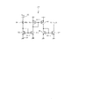
図1は、内燃機関のクランク角度およびその回転方向を検出する回転角検出装置の構成を示している。この回転角検出装置31は、センサチップ32(第1のチップに相当)、検出信号処理チップ33(第2のチップに相当)およびECU34(Electronic Control Unit)から構成されている。
(First embodiment)
Hereinafter, a first embodiment of the present invention will be described with reference to FIGS. 1 to 3.
FIG. 1 shows a configuration of a rotation angle detection device that detects a crank angle of an internal combustion engine and its rotation direction. The rotation
車両のクランクシャフトにはロータ(回転体)が固定されており、そのロータの外周部には所定間隔のパルス信号を生成するように複数の歯が設けられている。センサチップ32には、電源線35、36間に磁気抵抗素子(MRE)37、38を直列接続してなるフルブリッジ形態の第1のセンサ39と、電源線35、36間に磁気抵抗素子40、41を直列接続してなるフルブリッジ形態の第2のセンサ42とが形成されている。これらのセンサ39、42は、上記ロータに対向して配置されているとともに、互いに位相差を持つ信号を出力するようにロータの周方向にずらして配置されている。フルブリッジ型のセンサ39、42は、ハーフブリッジ型のセンサに比べ検出信号S1、S2の振幅が大きくなる利点がある。
A rotor (rotary body) is fixed to the crankshaft of the vehicle, and a plurality of teeth are provided on the outer periphery of the rotor so as to generate pulse signals at predetermined intervals. The
センサチップ32と検出信号処理チップ33との間は、ワイヤボンディングで形成された信号出力線43、44により接続されている。検出信号処理チップ33には、電源線35、36から電源電圧Vcc(例えば5V)の供給を受けて動作する検出信号処理回路45が形成されている。
The
コンパレータ46は、信号出力線43を介して入力される周期的なアナログ信号である第1の検出信号S1と、抵抗47、48により生成された基準電圧V1とを比較して、デジタル信号である検出信号B1を出力するようになっている。同様に、コンパレータ49は、信号出力線44を介して入力される周期的なアナログ信号である第2の検出信号S2と、抵抗50、51により生成された基準電圧V2とを比較して、デジタル信号である検出信号B2を出力するようになっている。なお、基準電圧V1、V2は、それぞれ検出信号S1、S2の変化幅の中央値に対応する2.5Vに設定されている。
The
検出信号処理回路45は、信号出力線44の断線を検出する断線検出回路52と、この断線検出回路52が信号出力線44の断線を検出したときに回転検出信号Sr(後述)の出力を停止するANDゲート53(断線処理回路に相当)とを備えている。断線検出回路52は、信号出力線44の検出信号処理チップ33側の端部(ノードN2)と電源線36(基準電圧線に相当)との間に接続された定電流回路54、しきい値電圧Va(例えば1.25V)を生成する抵抗55、56、およびノードN2における電圧としきい値電圧Vaとを比較するコンパレータ57(比較回路に相当)から構成されている。
The detection
ここで、定電流回路54は、高抵抗負荷回路に相当し、センサ42に流れる電流よりも十分に小さい微小電流を出力するようになっている。図2は、MOSFETを用いて構成した定電流回路54の一例を示している。FET82と83、FET84と85およびFET86と87は、それぞれ10:1のミラー比を持つカレントミラー回路を構成しており、抵抗81とFET82との直列回路で定まる電流(100μA)の1/1000の電流(0.1μA)が出力される。
Here, the constant
ANDゲート53は、上述した検出信号B1と、断線検出回路52から出力される断線検出信号Sbとを入力し、断線検出信号Sbのレベルに応じて検出信号B1の通過と遮断を制御するものである。
The AND
Dフリップフロップ58(保持回路に相当)は、第2の検出信号B2がLレベルからHレベルに変化した時点における第1の検出信号B1を保持するもので、D(データ)端子、CLK(クロック)端子、R/(リセット)端子には、それぞれ検出信号B1、検出信号B2、断線検出信号Sbが入力されている。ANDゲート59は、ANDゲート53の出力信号とDフリップフロップ58の非反転出力信号(信号QP)を入力とし、その出力信号によりトランジスタ61を駆動するようになっている。同様に、ANDゲート60は、ANDゲート53の出力信号とDフリップフロップ58の反転出力信号(信号QN)を入力とし、その出力信号によりトランジスタ62を駆動するようになっている。
The D flip-flop 58 (corresponding to a holding circuit) holds the first detection signal B1 when the second detection signal B2 changes from the L level to the H level, and has a D (data) terminal, a CLK (clock). ) Terminal and R / (reset) terminal are inputted with detection signal B1, detection signal B2, and disconnection detection signal Sb, respectively. The AND
トランジスタ61のコレクタは、抵抗63を介してトランジスタ62のコレクタに接続されており、そのトランジスタ62のコレクタは、信号出力線64により繋がるECU34の抵抗19を介して電源線35にプルアップされている。これらANDゲート59、60、トランジスタ61、62および抵抗19、63によりレベル変換回路65が構成されている。
The collector of the
図1に示すECU34は、クランク角の検出信号の他、カム角の検出信号、スロットル開度センサや燃焼圧センサ等からの検出信号などを入力して、所定の演算処理を実行するものである。このECU34における比較回路は、図8に示した比較回路28と同じ構成であるため同一の符号を付している。比較回路28は、信号出力線64における回転検出信号Srとしきい値電圧L1、L2とを比較して判定信号D1、D2を出力する。抵抗24、25により生成されるしきい値電圧L1と、抵抗26、27により生成されるしきい値電圧L2との間には、Vcc(Hレベル)>L1>Vm(Mレベル)>L2>0V(Lレベル)の関係が成立している。
The
次に、図3も参照しながら本実施形態の作用を説明する。
図3は、クランクシャフトのロータ(回転体)が正回転しているときの回転角検出装置31の波形図である。上から順に検出信号S1、S2、検出信号B1、検出信号B2、保持信号QP、ANDゲート59の出力信号、ANDゲート60の出力信号、回転検出信号Sr、判定信号D1、判定信号D2を表している。図3(a)は信号出力線43、44が断線していない場合であり、図3(b)は信号出力線44が断線している場合である。
Next, the operation of this embodiment will be described with reference to FIG.
FIG. 3 is a waveform diagram of the rotation
まず、信号出力線43、44が断線していない場合について説明する。
検出信号S1、S2は、それぞれロータの外周部に設けられた歯とセンサ39、42との離間距離に応じて、例えばVccの1/2である2.5Vを中心として数十mVの幅で周期的に変化する。センサ39、42は、ロータの周方向にずらして配置されているので、正転時には検出信号S1の位相が進み、逆転時には検出信号S2の位相が進む。2値化された検出信号B1、B2も同様の位相関係を持つ。
First, the case where the
The detection signals S1 and S2 have a width of several tens of mV, for example, about 2.5 V which is 1/2 of Vcc, depending on the distance between the teeth provided on the outer periphery of the rotor and the
このとき、電源線35から磁気抵抗素子40と信号出力線44とを介して定電流回路54に微小電流(0.1μA)が流れる。磁気抵抗素子40の抵抗は1kΩ程度であり、この微小電流が流れることによる検出信号S2に与える電圧変化は0.1mV程度となる。一方、検出信号S2は上述したように2.5Vを中心として数十mVの変化幅を持つため、定電流回路54を設けたことによる検出信号S2への影響は十分に小さくなる。
At this time, a minute current (0.1 μA) flows from the
断線検出回路52は、検出信号S2(ノードN2の電圧)と、その中心電圧2.5Vの1/2の電圧値を持つしきい値電圧Va(1.25V)とを比較し、Hレベル(非断線)の断線検出信号Sbを出力する。これに伴い、ANDゲート53は、検出信号B1をそのまま通過させる。
The
正転時には、保持信号QPがHレベル、保持信号QNがLレベルとなり、トランジスタ62はオフし、トランジスタ61は検出信号B1に従ってオンオフ動作する。抵抗19と63の抵抗値は等しいので、回転検出信号Srは、Hレベル(5V)とMレベル(2.5V)との間で変化する。比較回路28におけるしきい値電圧L1、L2を例えば3.75V、1.25Vとすれば、判定信号D1は回転検出信号Sr(検出信号B1)に同期して変化し、判定信号D2はLレベル一定となる。
During forward rotation, the holding signal QP is at the H level and the holding signal QN is at the L level, the
逆転時には、保持信号QPがLレベル、保持信号QNがHレベルとなり、トランジスタ62は検出信号B1に従ってオンオフ動作し、トランジスタ61はオフする。このとき、回転検出信号Srは、Hレベル(5V)とLレベル(0V)との間で変化し、判定信号D1、D2はともに回転検出信号Sr(検出信号B1)に同期して変化する。ECU34は、これら判定信号D1、D2に基づいて、クランク角度およびその回転方向を検出する。
At the time of reverse rotation, the holding signal QP becomes L level and the holding signal QN becomes H level, the
続いて、信号出力線43が接続されており、信号出力線44が断線した場合について説明する。
信号出力線44が断線すると、定電流回路54の作用によりノードN2の電圧が0Vに固定され、断線検出信号SbはLレベル(断線)になる。これにより、ANDゲート53はレベル変換回路65への検出信号B1の入力を遮断し、Dフリップフロップ58はリセットされる。このとき、ANDゲート59、60の出力信号はLレベルとなり、トランジスタ61、62はともにオフとなる。その結果、回転検出信号SrはHレベル一定となり、判定信号D1、D2はともにLレベル一定となる。
Next, a case where the
When the signal output line 44 is disconnected, the voltage of the node N2 is fixed to 0 V by the action of the constant
なお、信号出力線44が接続されており、信号出力線43が断線している場合には、断線検出信号SbはHレベル(非断線)となり、Dフリップフロップ58のCLK端子には矩形波状の検出信号B2が与えられる。しかしながら、検出信号B1がHレベル一定となるため、トランジスタ61がオン、トランジスタ62がオフとなり、回転検出信号SrはMレベル一定となり、判定信号D1はHレベル一定、判定信号D2はLレベル一定となる。
When the signal output line 44 is connected and the
つまり、信号出力線43、44の何れか一方が断線すると、判定信号D1、D2の変化が停止する。ECU34は、カム角の検出信号などに基づいて回転状態にあると判断しているにもかかわらず、クランクシャフトのロータ(回転体)が停止状態であると判断すると、異常状態であるとして所定のエラー処理を実行する。なお、上述した作用は逆転時でも同様となる。
That is, when one of the
以上説明したように、本実施形態の回転角検出装置31は、センサチップ32と検出信号処理チップ33とを接続する信号出力線44の断線を検出する断線検出回路52を備え、断線検出時には検出信号B1のレベル変換回路65への入力を遮断するように構成されているので、信号出力線44(ボンディングワイヤ)が断線した場合、回転検出信号Srひいては判定信号D1、D2における検出信号B1に同期したレベル変化が停止する。
As described above, the rotation
これにより、ECU34は、信号出力線43の断線時のみならず信号出力線44の断線時にも断線異常を検出可能となり、回転方向によらず判定信号D1、D2が正転(または反転)の状態を呈し続けることによる回転方向の誤検出を確実に防止できる。また、信号出力線43、44のうち信号出力線44の断線のみを検出する構成としているので、検出信号処理回路45の回路規模(検出信号処理チップ33のサイズ)を低減することができる。
Thereby, the
断線検出回路52を構成する定電流回路54は、MOSFETを用いて構成されているので、素子サイズを抑えながらミラー比を大きく設定でき、センサ42に流れる電流よりも十分に小さい微小電流を出力可能となる。その結果、定電流回路54の存在によるセンサ42への影響が小さくなり、検出信号S2の電圧誤差を十分に小さくできる。
Since the constant
Dフリップフロップ58のR/(リセット)端子に断線検出信号Sbが入力されているので、電源投入後でロータの回転開始時における判定信号D1、D2が一義的に確定する(不定状態とならない)。ただし、このリセット端子への入力は、本願発明において必ずしも必要なものではない。
Since the disconnection detection signal Sb is input to the R / (reset) terminal of the D flip-
(第2の実施形態)
次に、本発明の第2の実施形態について図4ないし図7を参照しながら説明する。
図4に示す回転角検出装置66は、図1に示す回転角検出装置31の断線検出回路52を間欠動作可能に構成したものである。検出信号処理チップ67には、間欠信号生成回路68とラッチ69を備えた検出信号処理回路70が形成されている。
(Second Embodiment)
Next, a second embodiment of the present invention will be described with reference to FIGS.
A rotation angle detection device 66 shown in FIG. 4 is configured such that the
間欠信号生成回路68は、検出信号B1のレベルが変化した時点から検出信号B2のレベルが変化する時点よりも前までの所定期間だけHレベルとなる間欠信号Scを生成するもので、図5に示す構成を備えている。電源線35と36との間には抵抗71と72が直列に接続されており、基準電圧Vbが生成されている。また、コンパレータ46の出力端子と電源線36との間には抵抗73とコンデンサ74が直列に接続されており、積分電圧Vcが生成されている。コンパレータ75は、これら基準電圧Vbと積分電圧Vcを入力し、ExORゲート76は、コンパレータ75の出力信号と検出信号B1を入力して間欠信号Scを出力するようになっている。
The intermittent
図6は、この間欠信号生成回路68の動作波形を示している。検出信号B1のレベルが変化すると、積分電圧Vcは、抵抗73の抵抗値とコンデンサ74の容量値とで定まる時定数で変化し、コンパレータ75の出力信号は検出信号B1に対して位相が遅れる。間欠信号Scは、この位相差に対応した期間だけHレベルとなる。
FIG. 6 shows an operation waveform of the intermittent
断線検出回路52の定電流回路54とコンパレータ57は、間欠信号ScがHレベルの期間だけ動作し、間欠信号ScがLレベルの期間では消費電流がほぼゼロとなる。ラッチ69は、間欠信号ScがHレベルのときに断線検出信号Sbをそのまま通過させ、間欠信号ScがLレベルになるとその直前の断線検出信号Sbのレベルを保持する。
The constant
図7は、間欠動作に係る各信号の波形図である。上から順に検出信号S1、S2、検出信号B1、検出信号B2、間欠信号Scを表している。間欠信号Scは、検出信号B1のレベルが変化した時点でLレベルからHレベルに変化し、その後に検出信号B2のレベルが変化する時点ではLレベルに戻っているパルス信号となる。 FIG. 7 is a waveform diagram of each signal related to the intermittent operation. The detection signals S1 and S2, the detection signal B1, the detection signal B2, and the intermittent signal Sc are shown in order from the top. The intermittent signal Sc is a pulse signal that changes from the L level to the H level when the level of the detection signal B1 changes, and then returns to the L level when the level of the detection signal B2 changes thereafter.
本実施形態の回転角検出装置66は、センサ42を構成する磁気抵抗素子40、41の抵抗値が高い等の理由で、定電流回路54の出力電流をセンサ42に流れる電流よりも十分に小さい電流にできない場合において特に有効となる。このような場合に定電流回路54を動作させると、検出信号S2の電圧が本来の電圧よりも低下して検出信号B2の位相にずれが生じ、Dフリップフロップ58が保持するレベルに誤りが生じる虞がある。
In the rotation angle detection device 66 of the present embodiment, the output current of the constant
本実施形態によれば、少なくとも検出信号B2のレベルが変化する時点では、定電流回路54の動作が停止しているので、定電流が流れることによる検出信号B2の電圧変動が発生せず、回転方向の誤検出を防止することができる。また、間欠信号Scにより定電流回路54およびコンパレータ57を含む断線検出回路52全体の動作を停止するので、これらの動作電流による電源電圧Vccの変動や低下もなく、より確実に回転方向を検出できるとともに、検出信号処理チップ67の消費電流を低減することができる。
According to the present embodiment, since the operation of the constant
(その他の実施形態)
なお、本発明は上記し且つ図面に示す各実施形態に限定されるものではなく、例えば以下のように変形または拡張が可能である。
センサは、抵抗性の検出素子を用いていればよく、例えば圧力センサ、加速度センサなどであってもよい。
カム軸の角度およびその回転方向を検出する回転角検出装置であってもよい。
定電流回路54に替えて高抵抗素子(高抵抗負荷回路に相当)を用いてもよい。ただし、定電流回路54を用いた方がレイアウトサイズが小さくなる利点がある。
信号出力線43、44のボンディングワイヤを複数本にするとよい。
(Other embodiments)
The present invention is not limited to the embodiments described above and shown in the drawings, and can be modified or expanded as follows, for example.
The sensor only needs to use a resistive detection element, and may be a pressure sensor, an acceleration sensor, or the like, for example.
A rotation angle detection device that detects the angle of the cam shaft and the rotation direction thereof may be used.
Instead of the constant
A plurality of bonding wires for the
32はセンサチップ(第1のチップ)、33、67は検出信号処理チップ(第2のチップ)、36は電源線(基準電圧線)、37、38、40、41は磁気抵抗素子、39、42はセンサ(第1、第2のセンサ)、43、44は信号出力線、45、70は検出信号処理回路、52は断線検出回路、53はANDゲート(断線処理回路)、54は定電流回路(高抵抗負荷回路)、57はコンパレータ(比較回路)、58はDフリップフロップ(保持回路)、65はレベル変換回路である。 32 is a sensor chip (first chip), 33 and 67 are detection signal processing chips (second chip), 36 is a power supply line (reference voltage line), 37, 38, 40 and 41 are magnetoresistive elements, 39, 42 is a sensor (first and second sensors), 43 and 44 are signal output lines, 45 and 70 are detection signal processing circuits, 52 is a disconnection detection circuit, 53 is an AND gate (disconnection processing circuit), and 54 is a constant current. A circuit (high resistance load circuit), 57 is a comparator (comparison circuit), 58 is a D flip-flop (holding circuit), and 65 is a level conversion circuit.
Claims (9)
前記第1、第2の検出信号を入力し、前記第2の検出信号が所定のレベル変化をした時点における前記第1の検出信号のレベルを保持する保持回路と、
この保持回路が保持している信号レベルに応じて前記第1の検出信号のレベルを変換し前記回転検出信号を生成するレベル変換回路と、
前記信号出力線の断線を検出する断線検出回路と、
この断線検出回路が前記信号出力線の断線を検出したときに、前記第1、第2の検出信号を前記保持回路に入力した状態で、前記レベル変換回路への前記第1の検出信号の入力を遮断することにより前記矩形波状の回転検出信号の出力を停止する断線処理回路とを備えたことを特徴とする検出信号処理回路。 Based on periodic first and second detection signals input from the first and second sensors disposed opposite to the rotating body so as to have a phase difference from each other via each signal output line, the rotating body In a detection signal processing circuit that generates a rectangular wave-shaped rotation detection signal having a signal level corresponding to the rotation direction of
A holding circuit that inputs the first and second detection signals and holds the level of the first detection signal at the time when the second detection signal changes by a predetermined level;
A level conversion circuit that converts the level of the first detection signal according to the signal level held by the holding circuit and generates the rotation detection signal;
A disconnection detection circuit for detecting disconnection of the signal output line;
When the disconnection detection circuit detects disconnection of the signal output line , the first detection signal is input to the level conversion circuit while the first and second detection signals are input to the holding circuit. A detection signal processing circuit comprising: a disconnection processing circuit that stops output of the rotation detection signal in the form of a rectangular wave by interrupting .
前記信号出力線と所定の基準電圧線との間に接続され、前記センサに流れる電流よりも小さい電流を流す高抵抗負荷回路と、
この高抵抗負荷回路が接続された信号出力線を介して入力される前記検出信号と所定のしきい値電圧とを比較する比較回路とから構成されていることを特徴とする請求項1記載の検出信号処理回路。 The disconnection detection circuit includes:
A high resistance load circuit that is connected between the signal output line and a predetermined reference voltage line and flows a current smaller than a current flowing through the sensor;
2. The comparison circuit according to claim 1, further comprising a comparison circuit for comparing the detection signal inputted through a signal output line connected to the high resistance load circuit with a predetermined threshold voltage. Detection signal processing circuit.
Priority Applications (1)
| Application Number | Priority Date | Filing Date | Title |
|---|---|---|---|
| JP2007165121A JP4862760B2 (en) | 2007-06-22 | 2007-06-22 | Detection signal processing circuit |
Applications Claiming Priority (1)
| Application Number | Priority Date | Filing Date | Title |
|---|---|---|---|
| JP2007165121A JP4862760B2 (en) | 2007-06-22 | 2007-06-22 | Detection signal processing circuit |
Publications (2)
| Publication Number | Publication Date |
|---|---|
| JP2009002840A JP2009002840A (en) | 2009-01-08 |
| JP4862760B2 true JP4862760B2 (en) | 2012-01-25 |
Family
ID=40319377
Family Applications (1)
| Application Number | Title | Priority Date | Filing Date |
|---|---|---|---|
| JP2007165121A Expired - Fee Related JP4862760B2 (en) | 2007-06-22 | 2007-06-22 | Detection signal processing circuit |
Country Status (1)
| Country | Link |
|---|---|
| JP (1) | JP4862760B2 (en) |
Families Citing this family (2)
| Publication number | Priority date | Publication date | Assignee | Title |
|---|---|---|---|---|
| JP6034575B2 (en) * | 2012-03-05 | 2016-11-30 | 株式会社デンソー | Sensor signal generator |
| JP6343922B2 (en) * | 2013-12-17 | 2018-06-20 | 矢崎総業株式会社 | Horn control device |
Family Cites Families (5)
| Publication number | Priority date | Publication date | Assignee | Title |
|---|---|---|---|---|
| JPH01307620A (en) * | 1988-06-07 | 1989-12-12 | Toshiba Corp | Detecting circuit for abnormality of pulse encoder |
| JPH0712589A (en) * | 1993-06-21 | 1995-01-17 | Matsushita Electric Ind Co Ltd | Malfunction detector for magnetic type encoder |
| JP3588044B2 (en) * | 2000-09-14 | 2004-11-10 | 三菱電機株式会社 | Magnetic detector |
| JP4232771B2 (en) * | 2005-09-30 | 2009-03-04 | 株式会社デンソー | Rotation detector |
| JP4486917B2 (en) * | 2005-10-24 | 2010-06-23 | アルプス電気株式会社 | Rotation angle detection sensor and failure detection circuit thereof |
-
2007
- 2007-06-22 JP JP2007165121A patent/JP4862760B2/en not_active Expired - Fee Related
Also Published As
| Publication number | Publication date |
|---|---|
| JP2009002840A (en) | 2009-01-08 |
Similar Documents
| Publication | Publication Date | Title |
|---|---|---|
| JP4964358B2 (en) | Rotation sensor detection signal processing apparatus and rotation sensor detection signal output method | |
| US7205761B2 (en) | Rotation state detecting device and rotation state detecting method | |
| JP5517777B2 (en) | System having disconnection detection circuit and disconnection detection means for bridge circuit | |
| JP5163963B2 (en) | Abnormality monitoring device | |
| JP2005249488A (en) | Detection signal processing circuit and detection signal processing device for rotation sensor | |
| JP6158682B2 (en) | Magnetic sensor circuit | |
| JP2009294172A (en) | Magnetic detection device | |
| JP4862760B2 (en) | Detection signal processing circuit | |
| JP2008141612A (en) | Fault detection apparatus for load driving device, and load driving ic | |
| JP4248998B2 (en) | Encoder | |
| JP3222017B2 (en) | Electronic water meter | |
| JP4480453B2 (en) | Rotation angle sensor | |
| JP4930528B2 (en) | Rotation angle detector | |
| JP2000114039A (en) | Device for detecting failure in linear solenoid | |
| JP2006112889A (en) | Power supply voltage detection circuit | |
| JP3697610B2 (en) | Encoder | |
| JP2018182798A (en) | Electronic control device | |
| JP5370915B2 (en) | Voltage limiting circuit | |
| JPH10170533A (en) | Rotation detecting system | |
| JP2020180929A (en) | Rotation sensor | |
| JP2008099356A (en) | Mode switching circuit | |
| JP6003809B2 (en) | Rotation detector | |
| JP5430388B2 (en) | Load control circuit | |
| JP2009093598A (en) | Power supply control circuit | |
| CN115023617A (en) | High resolution PWM wheel speed sensor protocol |
Legal Events
| Date | Code | Title | Description |
|---|---|---|---|
| A621 | Written request for application examination |
Free format text: JAPANESE INTERMEDIATE CODE: A621 Effective date: 20090602 |
|
| A977 | Report on retrieval |
Free format text: JAPANESE INTERMEDIATE CODE: A971007 Effective date: 20110411 |
|
| A131 | Notification of reasons for refusal |
Free format text: JAPANESE INTERMEDIATE CODE: A131 Effective date: 20110510 |
|
| A521 | Written amendment |
Free format text: JAPANESE INTERMEDIATE CODE: A523 Effective date: 20110531 |
|
| TRDD | Decision of grant or rejection written | ||
| A01 | Written decision to grant a patent or to grant a registration (utility model) |
Free format text: JAPANESE INTERMEDIATE CODE: A01 Effective date: 20111011 |
|
| A01 | Written decision to grant a patent or to grant a registration (utility model) |
Free format text: JAPANESE INTERMEDIATE CODE: A01 |
|
| A61 | First payment of annual fees (during grant procedure) |
Free format text: JAPANESE INTERMEDIATE CODE: A61 Effective date: 20111024 |
|
| FPAY | Renewal fee payment (event date is renewal date of database) |
Free format text: PAYMENT UNTIL: 20141118 Year of fee payment: 3 |
|
| FPAY | Renewal fee payment (event date is renewal date of database) |
Free format text: PAYMENT UNTIL: 20141118 Year of fee payment: 3 |
|
| R250 | Receipt of annual fees |
Free format text: JAPANESE INTERMEDIATE CODE: R250 |
|
| R250 | Receipt of annual fees |
Free format text: JAPANESE INTERMEDIATE CODE: R250 |
|
| R250 | Receipt of annual fees |
Free format text: JAPANESE INTERMEDIATE CODE: R250 |
|
| R250 | Receipt of annual fees |
Free format text: JAPANESE INTERMEDIATE CODE: R250 |
|
| LAPS | Cancellation because of no payment of annual fees |