JP4833103B2 - Component mounter - Google Patents
Component mounter Download PDFInfo
- Publication number
- JP4833103B2 JP4833103B2 JP2007025661A JP2007025661A JP4833103B2 JP 4833103 B2 JP4833103 B2 JP 4833103B2 JP 2007025661 A JP2007025661 A JP 2007025661A JP 2007025661 A JP2007025661 A JP 2007025661A JP 4833103 B2 JP4833103 B2 JP 4833103B2
- Authority
- JP
- Japan
- Prior art keywords
- substrate
- board
- transport
- mounting
- stage
- Prior art date
- Legal status (The legal status is an assumption and is not a legal conclusion. Google has not performed a legal analysis and makes no representation as to the accuracy of the status listed.)
- Active
Links
Images


Description
本発明は、複数の実装ステージを備え、各実装ステージにわたって被実装用の基板を順次搬送することができるようになっている部品実装機に関するものである。 The present invention relates to a component mounter that includes a plurality of mounting stages and is capable of sequentially transporting a substrate to be mounted across each mounting stage.
従来から、実装用ヘッドにより被実装用の基板に所要数の電子部品を実装する実装ステージと、この実装ステージに対して上記基板の搬入、搬出を行う搬送装置とを備えた部品実装機は一般に知られている。 2. Description of the Related Art Conventionally, a component mounting machine having a mounting stage for mounting a required number of electronic components on a substrate to be mounted by a mounting head and a transfer device for carrying the substrate in and out of the mounting stage is generally used. Are known.
特に実装効率を高めるため、下記の特許文献1に示されるように、複数の実装ステージを備えて、複数の基板に同時に電子部品を実装することができるようにするとともに、基板搬入部から各実装ステージおよび基板搬出部にわたって基板を順次搬送する搬送装置を設け、各実装ステージで実装を完了した複数の基板を同時に下流側へ搬送することができるようにした実装機も知られている。
この種の実装機において、搬送装置による基板搬送中に何らかの原因で基板が途中で引っ掛かったり搬送装置の動作不良が生じたりして、基板が搬送途中で停止することがある。このような基板搬送に関連する原因による故障が生じたとき、いったん実装機の運転が停止された後、故障原因を解消する作業が行われるとともに、搬送途中で停止した基板を正規の位置まで移動させる位置修正作業が行われてから、運転が再開される。 In this type of mounting machine, the substrate may be stopped in the middle of conveyance because the substrate may be caught in the middle or a malfunction of the conveyance device may occur during the conveyance of the substrate by the conveyance device. When a failure due to a cause related to board transportation occurs, after the operation of the mounting machine is stopped, work to eliminate the cause of the failure is performed, and the board stopped during transportation is moved to a normal position. The operation is resumed after the position correction work to be performed is performed.
この場合、上記位置修正作業は、従来、オペレータが手作業で行っていた。しかしながら、多数の実装ステージを備えた実装機においては、基板搬送路上の多数の基板が搬送されるため、その搬送中に故障が生じると、各基板の位置の確認や、各基板をそれぞれ正規の位置に移動させる作業が非常に煩雑なものとなる。 In this case, the position correction work has conventionally been performed manually by an operator. However, in a mounting machine equipped with a large number of mounting stages, a large number of substrates on the substrate transport path are transported, so if a failure occurs during the transport, the position of each substrate can be confirmed and each substrate can be The movement to the position becomes very complicated.
本発明はこのような事情に鑑みてなされたものであり、複数の実装ステージと各ステージわたって基板を搬送する基板搬送装置とを備えた部品実装機において、基板搬送に関連する原因による故障発生後に復旧して運転を再開するときに、基板搬送路上の基板を正規の位置に移動させる作業を自動的に行うことができ、復旧作業を簡単にすることができる部品実装機を提供することを目的とする。 The present invention has been made in view of such circumstances, and in a component mounter including a plurality of mounting stages and a substrate transport apparatus that transports a substrate across each stage, a failure occurs due to a cause related to substrate transport. Providing a component mounter that can automatically perform the work of moving the board on the board transport path to the proper position when it is later restored and restarted. Objective.
上記課題を解決するために、本発明の部品実装機は、基板搬送方向に並んでそれぞれ被実装用の基板に対する電子部品の実装作業を行う複数の実装ステージと、上記各実装ステージを通る基板搬送路上に設けられ、上記基板を基板搬送路の上流側の基板搬入部から上記各実装ステージを経て基板搬送路の下流側の基板搬出部へ順次搬送し、基板搬送路上の複数の基板を同時に搬送可能な基板搬送装置と、上記基板搬送装置に設けられて、基板搬送路上の基板を検知する基板検知センサと、上記基板搬送装置の駆動を制御する制御装置とを備え、上記制御装置は、基板搬送に関連する原因による故障発生後の運転再開時に、上記基板検知センサからの信号に基づいて基板搬送路上の基板の位置を検出する基板位置検出手段と、上記基板位置検出手段により検出された基板位置が正規の位置からずれている場合に上記基板搬送装置を駆動して基板を正規の位置に移動させるように制御する基板位置修正用制御手段とを有するものである。 In order to solve the above-described problems, a component mounting machine according to the present invention includes a plurality of mounting stages that perform mounting of electronic components on a substrate to be mounted side by side in the substrate transport direction, and substrate transport that passes through each of the mounting stages. The substrate is provided on the path, and the substrate is sequentially transferred from the substrate carry-in portion on the upstream side of the substrate transfer route to the substrate carry-out portion on the downstream side of the substrate transfer route through each mounting stage, and simultaneously transfers a plurality of substrates on the substrate transfer route A substrate transfer device, a substrate detection sensor that is provided in the substrate transfer device and detects a substrate on a substrate transfer path, and a control device that controls the drive of the substrate transfer device. Substrate position detection means for detecting the position of the substrate on the substrate transfer path based on a signal from the substrate detection sensor when restarting operation after the occurrence of a failure due to a cause related to transfer; and the substrate position detection Substrate position detected by stage in which a control means for the substrate position correction control to move the substrate by driving the substrate transfer apparatus to the normal position when displaced from the normal position.
この部品実装機によると、上記運転再開時に、基板検知センサからの信号に基づいた上記基板位置検出手段による基板位置の検出と、この基板位置の検出に応じた上記基板位置修正用制御手段による基板搬送装置の制御により、基板搬送路上の基板の位置修正が自動的に行われる。 According to this component mounting machine, when the operation is resumed, the board position is detected by the board position detection means based on the signal from the board detection sensor, and the board by the board position correction control means in accordance with the detection of the board position. The position of the substrate on the substrate transport path is automatically corrected by the control of the transport device.
この部品実装機において、上記基板搬送装置は、上記各実装ステージにわたって基板搬送路の方向に延び、この方向に移動可能な搬送軸と、該搬送軸を駆動する搬送軸駆動手段と、該搬送軸に各実装ステージごとに設けられて、各実装ステージの基板搬送路上の上記基板を押動する複数の押動部材と、該各押動部材を、上記搬送軸の移動に伴い基板を押動可能な基板押動位置と基板から離間する退避位置との間で位置変更させる押動部材駆動手段とを有し、上記搬送軸に基板検知センサが設けられていることが好ましい。 In this component mounting machine, the board transfer device extends in the direction of the board transfer path over the mounting stages, and is capable of moving in this direction, a transfer axis driving means for driving the transfer axis, and the transfer axis. Provided for each mounting stage, and a plurality of pushing members for pushing the substrate on the substrate carrying path of each mounting stage, and the pushing member can push the substrate as the carrying shaft moves. It is preferable that a pressing member driving means for changing the position between the substrate pressing position and the retracted position away from the substrate is provided, and a substrate detection sensor is provided on the transport shaft.
このようにすると、基板搬送時には、上記押動部材を基板押動位置とした状態で搬送軸を移動させることにより、基板が搬送される。また、上記基板位置検出手段による基板位置検出時には、各押動部材を退避位置とした状態で上記搬送軸を移動させつつ、上記基板検知センサからの信号を読み込むことにより、基板を捜索し、基板位置を検出することができる。 If it does in this way, at the time of substrate conveyance, a substrate will be conveyed by moving a conveyance axis in the state where the above-mentioned pushing member was made into a substrate pushing position. Further, when the substrate position is detected by the substrate position detecting means, the substrate is searched by reading a signal from the substrate detection sensor while moving the transport shaft in a state in which each pushing member is in the retracted position. The position can be detected.
このような構造において、上記搬送軸は実装ステージの1ステージ分に相当する可動範囲で基板搬送路の方向に往復移動可能となっており、上記基板検知センサは、実装ステージ間長さに対応するピッチで各実装ステージごとに設けられていることが好ましい。 In such a structure, the transport axis can be reciprocated in the direction of the substrate transport path within a movable range corresponding to one stage of the mounting stage, and the substrate detection sensor corresponds to the length between the mounting stages. Preferably, each mounting stage is provided at a pitch.
このようにすれば、搬送軸を1ステージ分移動させるだけで、基板搬送路上の各実装ステージおよび各ステージ間を含む所要範囲にわたって基板を捜索することができ、迅速に基板位置を検出することができる。 In this way, the substrate can be searched over the required range including each mounting stage and each stage on the substrate conveyance path by simply moving the conveyance axis by one stage, and the substrate position can be detected quickly. it can.
さらに、上記基板検知センサは、各実装ステージごとに一対ずつ設けられ、その一対の基板検知センサの間隔は上記基板の長さと略同一に調整されていることが好ましい。 Further, it is preferable that a pair of the substrate detection sensors is provided for each mounting stage, and the distance between the pair of substrate detection sensors is adjusted to be substantially the same as the length of the substrate.
このようにすれば、基板位置が正確に検出される。 In this way, the substrate position is accurately detected.
また、上記押動部材は、各実装ステージごとに一対ずつ設けられ、その一対の押動部材で基板搬送路上の基板を上流側、下流側の両側から挟んだ状態で搬送し得るように一対の押動部材の間隔が調整されていることが好ましい。 Further, a pair of the pushing members are provided for each mounting stage, and the pair of pushing members can transport the substrate on the substrate transport path in a state of being sandwiched from both the upstream side and the downstream side. It is preferable that the distance between the pressing members is adjusted.
このようにすれば、安定良く基板を搬送することができる。 In this way, the substrate can be transported stably.
さらに、基板位置修正用制御手段は、基板を正規の位置に移動させるための制御として、各実装ステージごとに一対ずつ設けられている押動部材の全てを基板押動位置とした状態で基板搬送路上の基板を一括に移動させる第1の位置修正用制御モードと、押動部材の全ての対についてそれぞれ上流側の押動部材のみを基板押動位置とした状態で基板搬送路上の基板を一括に移動させる第2の位置修正用制御モードと、一部の実装ステージに対応する押動部材のみを基板押動位置とした状態で基板搬送路上の基板を個別に移動させる第3の位置修正用制御モードとを、基板搬送路上の基板の位置ずれの状況に応じて選択的に実行するようになっていることが好ましい。 Further, the substrate position correction control means transfers the substrate in a state where all of the pair of pressing members provided for each mounting stage are set to the substrate pressing position as control for moving the substrate to a normal position. The first position correction control mode for collectively moving the substrates on the path and the substrates on the substrate transport path in a state where only the upstream side pressing member is set to the substrate pressing position for all pairs of the pressing members. And a second position correction control mode in which the substrates on the substrate transport path are individually moved in a state where only the pressing members corresponding to some mounting stages are set to the substrate pressing position. It is preferable that the control mode is selectively executed according to the state of the positional deviation of the substrate on the substrate transport path.
このようにすれば、可能な限り複数の基板を一括で移動させて、迅速に位置修正を行うことができる。 In this way, it is possible to quickly correct the position by moving a plurality of substrates at once as much as possible.
以上のように、本発明の部品実装機によると、基板搬送に関連する原因による故障発生後の運転再開時に、基板搬送路上の基板の位置修正を自動的に行うことができるため、作業者が手作業で基板位置の修正を行う必要がなく、基板搬送路に多数の基板が存在している場合でも煩雑な位置修正作業を行う必要がない。従って、運転再開のための作業が非常に簡単になる。 As described above, according to the component mounter of the present invention, the position of the board on the board transport path can be automatically corrected when the operation is resumed after the occurrence of a failure due to a board transport related cause. There is no need to manually correct the substrate position, and there is no need to perform complicated position correction work even when a large number of substrates are present in the substrate transport path. Therefore, the work for resuming the operation becomes very simple.
本発明の好ましい実施の形態について図面を用いて説明する。 A preferred embodiment of the present invention will be described with reference to the drawings.
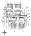
図1は本発明の一実施形態による部品実装機(以下、略して実装機という)の概略構成を示す平面図、図2は実装機の詳細構造を示す平面図、図3は図2におけるIII−III線断面図である。 FIG. 1 is a plan view showing a schematic configuration of a component mounting machine (hereinafter referred to simply as a mounting machine) according to an embodiment of the present invention, FIG. 2 is a plan view showing a detailed structure of the mounting machine, and FIG. FIG.
これらの図において、実装機1は、上流側端部(一端部)から下流側端部(他端部)に向けてプリント基板(被実装用の基板)3を送り、この搬送方向に並べられた第1〜第4の実装ステージ4〜7によってプリント基板3に電子部品(図示せず)をそれぞれ実装するものである。なお、以下においては、上記搬送方向と平行な方向をX方向、これと直交する方向を単にY方向という。
In these drawings, the
実装機1は、後述する各装置を支持するための基台11と、上述した4つの実装ステージ4〜7と、上流側端部に隣接する図外の上流側機器からプリント基板3を受け取って最上流に位置する第1の実装ステージ4に送るための搬入装置12が設けられた搬入ステージ(基板搬入部)8と、最下流に位置する第4の実装ステージ7からプリント基板3を受け取って、図外の後工程を行う下流側機器に搬出するための搬出装置13が設けられた搬出ステージ(基板搬出部)9と、これらのステージ間でプリント基板3をX方向に移動させるための基板搬送装置51とを備えている。
The
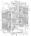
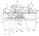
上記基台11上には、第1〜第6のYフレーム16〜21が設けられている。これら第1〜第6のYフレーム16〜21は、図1および図2に示すように、基台11上のX方向所定間隔おきの6箇所にそれぞれ、Y方向に延びるように設けられている。これらのYフレーム16〜21のうち、搬送方向の上流側から1番目と、3番目および5番目に位置する第1、第3、第5のYフレーム16,18,20は、基台11におけるY方向の一端部(以下、この端部を装置前側という)から他端側(装置後側)に延び、他方の第2、第4および第6のYフレーム17,19,21は、装置後側となるY方向の端部から装置前側に延びるように形成されている。Yフレーム18,20の前側端部およびYフレーム17,19の後側端部は、装置Y方向中央部の後記搬送軸52の配置箇所付近に達している。また、これら第1〜第6のYフレーム16〜21における基台11のY方向の中央部と対応する部位には、図3に示すように、プリント基板3を通すための凹部22が形成されている。
On the
上記4つの実装ステージ4〜7は、基台11上において搭載される位置、部材の配置方向などが異なる他は同じ構造となるように形成されている。このため、ここにおいては、最も上流側に位置する第1の実装ステージ4について説明し、他の実装ステージ5〜7については、同一符号を付し詳細な説明は省略する。
The four
実装ステージ4は、図2および図3に示すように、プリント基板3を後述の搬送位置と実装位置との間でY方向に移動させる移送手段23と、この移送手段23のY方向一側方(装置前側)に隣接するように設けられた多数のテープフィーダー24,24‥‥からなる電子部品供給装置25と、上記テープフィーダー24から電子部品をプリント基板3に移載するための電子部品移載装置26とを備えている。
2 and 3, the
上記移送手段23は、図3に示すように、基台11上にY方向に延びるように設けられた一対のガイドレール31,31と、これらのガイドレール31に移動自在に支持されたテーブル32と、このテーブル32をY方向に移動させるY方向駆動装置33と、上記テーブル32の上に設けられたコンベア34と、上記テーブル32に対するプリント基板3の移動を規制するためのクランプ機構35とから構成されている。
As shown in FIG. 3, the transfer means 23 includes a pair of
上記Y方向駆動装置33は、基台11上にY方向に延びる状態で回転自在に支持されたボールねじ軸33aと、このボールねじ軸33aを回転させるモータ33bと、上記ボールねじ軸33aに螺合するとともにテーブル32に固定されたボールナット33c等を備えている。このY方向駆動装置33は、上記テーブル32を図1中に実線で示す搬送位置と、図1中に二点鎖線で示す実装位置との間で往復動させることができるように構成されている。上記搬送位置は、基台11のY方向の中央部に位置付けられ、上記実装位置は、テープフィーダー24に近接する位置に位置付けられている。
The Y-
上記コンベア34は、一対の無端ベルト34aによって構成され、プリント基板3のY方向の両端部を支承し、このプリント基板3が後述する基板搬送装置51の駆動によりX方向(搬送方向)に押圧されることによって回転させられる。
The
上記クランプ機構35は、図3に示すように、プリント基板3のY方向の両端部の上方に位置する一対の受圧部材35a,35aと、プリント基板3を下方から押し上げて上記受圧部材35aに押し付けるための押し上げ装置35bとから構成されており、上記テーブル32に支持されている。
As shown in FIG. 3, the
上記第1の実装ステージ4の電子部品移載装置26は、図2および図3に示すように、上記第1、第3のYフレーム16,18の上端部にY方向に延びるように設けられた一対の第1のガイドレール41,41と、これらの第1のガイドレール41,41間に横架されてX方向に延び、かつ第1のガイドレール41に移動自在に支持された支持部材42と、この支持部材42を駆動する一対のY方向駆動装置43,43と、上記支持部材42に設けられてX方向に延びる第2のガイドレール44と、この第2のガイドレール44に移動自在に支持されたヘッドユニット45と、このヘッドユニット45を駆動するX方向駆動装置46と、上記ヘッドユニット45にZ軸モータ47等からなる昇降装置(図3参照)を介して昇降可能に支持された複数の吸着ヘッド48等によって構成されている。上記吸着ヘッド48は、図3に示すように、電子部品を吸着する吸着ノズル48aと、この吸着ノズル48aを上下方向の軸線回りに回動させるためのR軸モータ48b等からなる回転駆動装置とを備えている。
As shown in FIGS. 2 and 3, the electronic
上記Y方向駆動装置43は、第1、第3のYフレーム16,18の一端部(装置前側の端部)に固定されたモータ43aと、このモータ43aに一端部が接続されてY方向に延び、Yフレーム16,18に回転自在に支持されたボールねじ軸43bと、上記支持部材42に回転自在に支持されるとともに上記ボールねじ軸43bに螺合したボールナット43c(図3参照)などによって構成されている。
The Y-
上記X方向駆動装置46は、上記支持部材42におけるX方向の一端部に固定されたモータ46aと、このモータ46aに一端部が接続されてX方向に延び、支持部材42に回転自在に支持されたボールねじ軸46bと、上記ヘッドユニット45に回転自在に支持されるとともに上記ボールねじ軸46bに螺合したボールナット(図示せず)などによって構成されている。
The
この実施の形態による電子部品移載装置26は、上記吸着ヘッド48をX方向とY方向とに移動させて電子部品をテープフィーダー24から実装位置にあるプリント基板3に移載する。
The electronic
また、この電子部品移載装置26のヘッドユニット45には、図1〜図3には図示していないが、実装位置に位置付けられたプリント基板3の位置を検出するための撮像装置(図6中に示す基板カメラ79)と、吸着ノズル48aに吸着された電子部品の位置を検出するための撮像装置(図6中に示す部品カメラ80)とが設けられている。なお、この撮像装置は基台11に設けることもできる。
Further, although not shown in FIGS. 1 to 3, the
このように構成された実装ステージ4〜7は、図1および図2に示すように、基台11上に平面視において搬送方向の上流側から下流側に向けて千鳥足状に並ぶ状態で搭載されている。そして、図1に示すように、各々の移送手段23のテーブル32(プリント基板3)を搬送位置に移動させた状態では、これらのテーブル32上のコンベア34がY方向の同一位置に位置するように(X方向に一列に並ぶように)基台11上に配設されている。
As shown in FIGS. 1 and 2, the mounting
各実装ステージ4〜7の上記テーブル32は、搬送位置に位置付けられた状態において、互いに近接する位置に設けられている。そして、テーブル32上のコンベア34上に載せられているプリント基板3は、搬送方向の上流側から押されることにより、上流側のコンベア34から下流側のコンベア34に直接移動する。このプリント基板3の駆動は、後述する基板搬送装置51によって行われる。
The table 32 of each of the mounting
この実施の形態による実装機1においては、上述したように搬送位置に移動した各実装ステージ4〜7のテーブル32上のコンベア34によって、図1に示すように、基台11のY方向の中央部においてX軸方向に延びる基板搬送路50が構成される。
In the mounting
上記基板搬送装置51は、図2中および図3中に示すとともに図4に模式的に示すように、基板搬送路50の上方に配置された搬送軸52と、この搬送軸52をX軸方向に移動させる搬送軸駆動機構と、搬送軸52から下方に延びる実装ステージごとの押動部材53a,53bと、この押動部材53a,53bを駆動する押動部材駆動機構と、基板検知センサ56a,56bとを備えている。
As shown in FIGS. 2 and 3 and schematically shown in FIG. 4, the
上記搬送軸52は、各実装ステージ4〜7にわたってX軸方向に延びている。また、上記搬送軸駆動機構は、モータ54および伝動機構等で構成され、実装ステージの1ステージ分に相当する所定ストロークだけ搬送軸52をX軸方向の下流側、上流側に往復移動させることができるようになっている。
The
上記押動部材53a,53bは、各実装ステージごとに一対ずつ、ステージ間の長さに対応するピッチで配置されている。そして、各押動部材53a,53bは、搬送軸の移動に伴い基板を押動可能な基板押動位置と基板から離間する退避位置との間で位置変更となっている。具体的に説明すると、各押動部材53a,53bはそれぞれ、搬送軸52から下方に突出してプリント基板3に隣接する基板押動位置と、プリント基板3より上昇する退避位置との間で昇降可能とされ、あるいは、上記基板押動位置に相当する起立状態と上記退避位置に相当する倒伏状態との間で起伏可能とされている。
A pair of the
また、押動部材駆動機構は、モータ55等からなり、各押動部材53a,53bに対してそれぞれ設けられ、各押動部材53a,53bを基板押動位置退避位置との間で位置変更(昇降または起伏)させるようになっている。
The pushing member driving mechanism includes a
そして、搬送時には、押動部材53a,53bが退避位置(倒伏状態)とされるとともに、搬送軸52が可動範囲の上流側に位置しており(図4(a)参照)、基板搬送路50上のプリント基板3を搬送するときには、押動部材53a,53bが基板押動位置とされた状態で搬送軸52が下流側へ移動(往動)することにより、押動部材53a,53bが基板搬送路50上のプリント基板3を下流側へ押動し(図4(b)(c)参照)、搬送後は押動部材53a,53bが退避位置とされるとともに搬送軸52が上流側へ移動(復動)することにより、初期位置(図4(a))に戻されるようになっている。
At the time of transport, the pushing
なお、一対の押動部材53a,53bのうちの一方が基板搬送方向に位置変更可能とされることにより押動部材53a,53bの間隔が可変とされ、搬送されるプリント基板3に応じ、その長さに対応するように押動部材53a,53bの間隔が調整されるようになっている。そして、一対の押動部材53a,53bが基板押動位置とされたときに基板搬送路50上のプリント基板3を上流側、下流側の両側から挟んだ状態で搬送できるようになっている。つまり、一対のうちの上流側の押動部材53aでプリント基板3を押圧するとともに、下流側の押動部材53bでプリント基板3をずれないように保持しつつ、プリント基板3を搬送することができるようになっている。
In addition, the position of one of the pair of pressing
また、当実施形態では押動部材53a,53bが5対設けられ、搬送軸52が可動範囲の上流側に位置しているときは5対の押動部材53a,53bが搬入ステージ8と各実装ステージ4〜7に対応し、搬送軸52が可動範囲の下流側に移動したときは5対の押動部材53a,53bが各実装ステージ4〜7と搬出ステージ9とに対応するように配置されている。
Further, in this embodiment, five pairs of
このようにして、基板搬送装置51の作動によりプリント基板3を搬入ステージ8から各実装ステージ4〜7を経て搬出ステージ9へ1ステージ分ずつ順次搬送するとともに、基板搬送路上のプリント基板3を1つでも複数同時でも搬送することができるように、基板搬送装置51が構成されている。つまり、基板搬送路上の1つのプリント基板3のみを下流側に搬送したいときには、当該基板に対応する一対の押動部材53を基板押動位置とした状態で搬送軸52を下流側へ移動させることで当該基板を搬送することができ、また、複数のステージでそれぞれ搬送位置に移動させられた複数のプリント基板3が基板搬送路上に位置している状態でこれらを下流側に移動させたいときには、その各プリント基板3に対応する複数対の押動部材53を基板押動位置とした状態で搬送軸52を下流側へ移動させることでこれら複数のプリント基板3を同時に搬送させることができる。そして、当実施形態では最大5枚のプリント基板3を同時に搬送させることができるようになっている。
In this way, the printed
なお、前述のコンベア34の無端ベルト34aは回転自在であり、また、後述の搬入、搬出装置12,13のコンベア62の無端ベルト62aも非駆動時(基板の搬入又は搬出のための駆動時以外)は回転自在となっているため、基板搬送装置51による基板搬送時に、搬送されるプリント基板3に接する無端ベルトはプリント基板3の移動に伴って回転するようになっている。
The
また、上記基板検知センサ56a,56bは、プリント基板3の上方に位置したときにプリント基板3を検知するもので、例えば反射型の光センサ等で構成されている。そしてこの基板検知センサ56a,56bも上記押動部材53a,56bと同様に、各実装ステージごとに一対ずつ設けられ、当実施形態では5対設けられている。
The
図5に示すように、センサペア(基板検知センサ56a,56bの対)はステージ間長さL1と同一のピッチで配設されている。また、基板検知センサ56a,56bは押動部材53a,53bに近接して配置され、かつ、押動部材53a,53bに連動して基板検知センサ56a,56bの間隔が可変とされ、搬送されるプリント基板3の長さL2と略等しくなる(若干小さくなる)ように基板検知センサ56a,56bの間隔が調整されている。
As shown in FIG. 5, sensor pairs (a pair of
この基板搬送装置51の駆動は、制御装置としての後述のコントローラ70(図6参照)によって制御されるようになっている。
The driving of the
また、搬入ステージ8に設けられた搬入装置12と搬出ステージ9に設けられた搬出装置13は、図2に示すように、基台11上にY方向に移動可能に設けられたテーブル61と、このテーブル61の上に搭載されたコンベア62と、テーブル61をY方向に移動させるY方向駆動装置63から構成されている。これらの搬入、搬出装置12,13のY方向駆動装置63は、上記基板搬送路50上に位置する搬送位置と、基板搬送路50から装置前側(図2においては下側)に離間した搬入・搬出位置との間でテーブル61を移動させる構成が採られている。
Further, as shown in FIG. 2, the carry-in
搬入、搬出装置12,13のコンベア62は、プリント基板3のY方向の両端部を支持する無端ベルト62a,62aと、これらの無端ベルト62a,62aを回転させるための駆動装置(図示せず)とを備えている。そして、図外のクラッチ機構により、上流側機器からの基板搬入時には搬入装置12のコンベア62の無端ベルト62a,62aが駆動装置に接続され、また、下流側機器への基板搬出時には搬出装置13のコンベア62の無端ベルト62a,62aが駆動装置に接続されて、これらのときには駆動装置によるコンベア62の駆動が行われ、それ以外のときは無端ベルト62a,62aが駆動装置から切り離されて回転自在とされるようになっている。
The
また、上記コンベア62は、Y方向の一端側に位置する無端ベルト62aのY方向の位置をプリント基板3の幅に合わせて変えることができるように、幅調整機構(図示せず)を備えている。
Further, the
上記コンベア62は、搬送位置に位置している状態で隣接する第1または第4の実装ステージ4,7のコンベア34との間でプリント基板3が直接移動することができるように、第1、第4の実装ステージ4,7のコンベア34とX方向に近接する位置に配設されている。
The
上記搬入装置12は、図1に示すように、上記コンベア62が搬入位置に移動している状態で前工程を行う上流側機器に接続されるように構成され、搬出装置13は、コンベア62が搬出位置に移動している状態で後工程を行う下流側機器に接続されるように構成されている。
As shown in FIG. 1, the carry-in
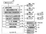
図6は、上記実装機1に設けられたコントローラ(制御装置)70の構成を示している。
FIG. 6 shows a configuration of a controller (control device) 70 provided in the mounting
この図において、コントローラ70は、CPU等で構成される演算処理部71と、実装プログラムを記憶する実装プログラム記憶部72と、基板搬送等のための各種データを記憶する搬送系データ記憶手段73と、ヘッドユニット45及び吸着ヘッド48を駆動するX軸、Y軸、Z軸、R軸の各モータ46a,43a,47,48b、並びに基板搬送装置51における搬送軸駆動機構のモータ54および押動部材駆動機構のモータ55を制御するモータ制御部74と、外部入出力部75と、画像処理部76とを有している。
In this figure, a
上記モータ制御部74は、演算処理部71からの指令に基づいて上記各モータの制御を行うようになっている。上記外部入出力部75には、入力要素として各種センサ類77が接続される一方、出力要素として各種駆動部等78が接続されている。
The
上記画像処理部76には、基板カメラ79及び部品カメラ80が接続され、これらのカメラからの画像信号が画像処理部76に取込まれて、所定の画像処理が施された上で、その画像データが演算処理部71に送られるようになっている。
A
演算処理部71は、基板搬送時における基板搬送装置51のモータ54,55の制御や、実装作業時におけるヘッドユニット45及び吸着ヘッド48の作動のためのモータ46a,43a,47,48bの制御を、モータ制御部74を介して行うとともに、各種駆動部等の制御を、外部入出力部75を介して行い、また、外部の表示ユニット81に対して信号を送信する。
The
さらに演算処理部71は、基板搬送に関連する原因による故障発生後の運転再開時の制御のために基板位置検出手段82および基板位置修正用制御手段83の機能を有している。
Further, the
上記基板位置検出手段82は、基板搬送に関連する原因による故障発生後の運転再開時に、搬送軸52とともに基板検知センサ56a,56bを移動させつつ、基板検知センサからの信号の変化を調べることにより、基板位置を検出する。
The substrate position detecting means 82 checks the change in the signal from the substrate detection sensor while moving the
すなわち、図7に示すように、基板搬送路50上のプリント基板3に対して搬送軸52が上流側から移動すると、先ずセンサペアのうちの一方のセンサ(下流側のセンサ)56bのみがオンとなり、次にこのセンサ56bがプリント基板3の下流端まで移動すると両センサ56a,56bがオンとなり、さらに搬送軸52が移動するすると他方のセンサ56aのみがオンとなる。
That is, as shown in FIG. 7, when the
そこで、両センサ56a,56bがオンとなった位置が、プリント基板の位置として検出される。
Therefore, the position where both
また、基板位置修正用制御手段83は、基板位置検出手段82によって検出された基板位置が正規の位置からずれている場合に、基板搬送装置51の搬送軸駆動機構(モータ54)および押動部材駆動機構(モータ55)を駆動して、プリント基板を正規の位置に移動させるように制御する。
Further, the substrate position correcting control means 83 is configured to provide a transport shaft driving mechanism (motor 54) and a pushing member of the
当実施形態では、プリント基板3を正規の位置に移動させる制御として、後に詳述するように、5対の押動部材53a,53bの全てを基板押動位置とした状態で基板搬送路50上の複数のプリント基板3を一括に移動させる第1の位置修正用制御モードと、5対それぞれにおける上流側の押動部材53aのみを基板押動位置とした状態で基板搬送路50上の複数のプリント基板3を一括に移動させる第2の位置修正用制御モードと、一部の実装ステージに対応する押動部材53a,53bのみを基板押動位置とした状態で基板搬送路50上のプリント基板を個別に移動させる第3の位置修正用制御モードとを、基板搬送路50上のプリント基板3の位置ずれの状況に応じて選択的に実行するようになっている。
In the present embodiment, as the control for moving the printed
上記演算処理部71の基板位置検出手段82および基板位置修正用制御手段83としての処理の具体例を図8および図9のフローチャートによって説明する。
A specific example of the processing of the
図8は全体フローを示す。このフローチャートでは、先ずプリント基板3の搬送が開始され(ステップS1)、それから、基板搬送に関連するエラー(故障)が発生したか否かが判定される(ステップS2)。
FIG. 8 shows the overall flow. In this flowchart, first, the conveyance of the printed
エラーが発生していなければ、搬送が継続されて、プリント基板3が下流側のステージまで搬送されることで搬送が完了し(ステップS3)、次いで実装が開始され、所要数の電子部品が実装されると実装終了となり、リターンする。そして、下流側へのプリント基板3の搬送と、実装ステージ4〜7での実装とが繰り返される。
If no error has occurred, the conveyance is continued, and the conveyance is completed by conveying the printed
ステップS2でエラー発生が判別されたときは、マシン(実装機)の運転が停止される(ステップS6)。そして、作業者によりエラーの原因を取り除くなどの復旧作業が行われた後、マシンの運転が再開される(ステップS7)。 When it is determined in step S2 that an error has occurred, the operation of the machine (mounting machine) is stopped (step S6). Then, after the operator performs recovery work such as removing the cause of the error, the operation of the machine is resumed (step S7).
この運転再開に際し、後述の搬送路上基板捜索移動処理(ステップS8)が行われる。この処理の完了(ステップS9)の後は、ステップS4に移行して、実装が開始される。 When the operation is resumed, a substrate search and movement process (step S8), which will be described later, is performed. After completion of this process (step S9), the process proceeds to step S4 and mounting is started.
図9は、上記ステップS8で行われる搬送路上基板捜索移動処理のルーチンを示している。なお、この処理は、上記運転再開時に自動的に実行され、あるいは、エラー発生によるマシン運転停止後に、表示ユニット81の操作画面上の「基板捜索ボタン」を押すことにより、自動的に実行される。
FIG. 9 shows a routine of the substrate search / transfer process on the transport path performed in step S8. This process is automatically executed when the operation is resumed, or is automatically executed by pressing the “board search button” on the operation screen of the
この処理がスタートすると、搬送軸捜索(基板捜索のための搬送軸52の移動)が開始され(ステップS11)、図7に示すように、搬送軸52を移動させつつセンサペア(56a,56b)からの信号の変化を調べることによる基板捜索が行われる。そして、5対の基板検知センサ56a,56bを上流側から順に第1〜第5センサペアと呼ぶと、第1〜第5センサペアの各々について、センサペアがプリント基板3を発見したか否かが判定される(ステップS12〜S16)。当実施形態では、センサペアの両センサ56a,56bが同時にオンとなったときにプリント基板3が発見されたこととなる。
When this process is started, a transport axis search (movement of the
上記各センサペアごとに、プリント基板3が発見されるとその発見位置(発見時点の搬送軸52の位置)が記憶される(ステップS17〜S21)。
When the printed
このようにして基板位置の検出(基板位置検出手段82としての処理)が行われた後、各センサペアによる基板発見位置に基づき、発見されたプリント基板3ごとの基板ピッチおよび基板間隔が計算される(ステップS22)。
After the substrate position is detected in this way (processing as the substrate position detecting means 82), the substrate pitch and the substrate interval for each discovered printed
次に、基板位置修正用制御手段83による制御が行われる。この制御を、図10〜図12の動作説明図を参照しつつ説明する。 Next, control by the substrate position correction control means 83 is performed. This control will be described with reference to the operation explanatory diagrams of FIGS.
基板位置修正用制御手段83による制御としては、上記ステップS22での計算に基づいて基板搬送路50上のプリント基板3の位置ずれの状況(特に各基板の位置関係)が調べられ、先ず、全センサペアの基板発見時の搬送軸52の位置が同じ位置か否かが判定される(ステップS23)。
As the control by the substrate position correcting control means 83, the state of positional deviation of the printed
この判定がYESであれば、各プリント基板3が各センサペアと同じピッチで並んでいることを意味する。この場合は、第1の位置修正用制御モードとしてステップS24〜S26が実行され、図10に示すように搬送軸52および押動部材53a,53bが制御される。
If this determination is YES, it means that the printed
すなわち、基板発見位置に搬送軸52が移動し(ステップS24)、続いて図10(a)に示すように全ての押動部材53a,53bが基板押動位置まで下降する(ステップS25)。それから、図10(b)に示すように搬送目標位置(正規の基板位置)に搬送軸52が移動する(ステップS26)。これらの動作が行われるように基板搬送装置51が制御されることにより、発見された複数のプリント基板3が一括に搬送される。
That is, the
上記ステップS23の判定がNOの場合は、基板ピッチのばらつきが所定以下で、かつ、各基板間隔が上流側押動部材53aを下降させる余裕が有るか否かが判定される(ステップS27)。
If the determination in step S23 is NO, it is determined whether or not the variation in the substrate pitch is equal to or less than a predetermined value and each substrate interval has a margin for lowering the
この判定がYESの場合は、第2の位置修正用制御モードとしてステップS26〜S28が実行され、図11に示すように搬送軸52および押動部材53a,53bが制御される。
If this determination is YES, steps S26 to S28 are executed as the second position correction control mode, and the conveying
すなわち、発見基板に対して押動部材ペアのうちの上流側押動部材53aが下降可能な位置に搬送軸52が移動し(ステップS28)、続いて図11(a)に示すように基板発見位置の上流側押動部材53aの全てが基板押動位置まで下降する(ステップS29)。それから、図11(b)に示すように搬送目標位置に搬送軸52が移動する(ステップS30)。これらの動作が行われるように基板搬送装置51が制御されることにより、発見された複数のプリント基板3が一括に搬送される。
That is, the
上記ステップS27の判定がNOの場合、第3の位置修正用制御モードとしてステップS31〜S34が実行され、図12に示すように搬送軸52および押動部材53a,53bが制御される。
When the determination in step S27 is NO, steps S31 to S34 are executed as the third position correction control mode, and the
すなわち、先ず最下流のセンサペアの基板発見位置に搬送軸52が移動するように制御され、続いて図12(a)に示すように対象とするセンサペアの基板発見位置に対応する押動部材53a,53bが基板押動位置まで下降し(ステップS32)、それから、図12(b)に示すように搬送目標位置に搬送軸52が移動する(ステップS33)。さらに全ての発見基板の搬送が完了したか否かが判定され(ステップS34)、完了していなければステップS31に戻ってそれ以下の処理が再び行われることにより、図12(c)(d)のように最下流から2番目のプリント基板に対して上記ステップS32〜S34の処理が行われる。そして、全ての発見基板の搬送が完了するまでこれらの動作が繰り返されるように基板搬送装置51が制御されることにより、基板搬送路50上のプリント基板3が下流側から順に個別に目標位置へ搬送される。
That is, first, the
以上のような当実施形態の実装機によると、基板搬送中に何らかの原因でプリント基板3が途中で引っ掛かったり基板搬送装置51の動作不良が生じたりして、プリント基板3が搬送途中で停止するような故障が発生した後、故障原因を除去する復旧作業が行われからの運転再開時に、基板位置検出手段82による基板位置の検出とそれに基づく基板位置修正用制御手段83による基板搬送装置51の制御により、基板搬送路50上の複数の基板の位置修正が自動的に行われる。
According to the mounting machine of the present embodiment as described above, the printed
従って、作業者が手作業で基板位置の修正を行う必要がなく、運転再開のための作業が非常に簡単になる。 Therefore, it is not necessary for the operator to manually correct the substrate position, and the operation for resuming the operation becomes very simple.
特に当実施形態では、上記搬送軸52に実装ステージごとに一対ずつの基板検知センサ56a,56bが設けられることにより、迅速に、かつ、正確に基板位置を検出することができる。
In particular, in this embodiment, a pair of
また、基板位置の検出に基づく基板位置修正のための処理として、基板搬送路50上のプリント基板3の位置ずれの状況に応じ、前述の第1の位置修正モード(ステップS24〜S26)、第2の位置修正モード(ステップS28〜S30)、第3の位置修正モード(ステップS31〜S34)のいずれかを選択的に実行するようにしているため、可能な限り複数の基板を一括で移動させて、迅速に位置修正を行うことができる。
Further, as the processing for correcting the substrate position based on the detection of the substrate position, the first position correction mode (steps S24 to S26) described above, the first position correction mode according to the state of positional deviation of the printed
なお、本発明の実装機の具体的構成は上記実施形態に限定されず、種々変更可能である。 In addition, the specific structure of the mounting machine of this invention is not limited to the said embodiment, A various change is possible.
例えば、押動部材は各実装ステージごとに1個ずつ(上流側押動部材53aに相当するもののみ)設けておいてもよいが、上記実施形態のように一対ずつ設けておけば、より安定よくプリント基板を搬送することができる。
For example, one pushing member may be provided for each mounting stage (only the one corresponding to the
また、実装ステージは、上記実施形態のように4つに限らず、要求に応じて適宜増減してもよい。 Further, the number of mounting stages is not limited to four as in the above embodiment, and may be appropriately increased or decreased according to the request.
1 部品実装機
3 プリント基板
4〜7 実装ステージ
8 搬入ステージ
9 搬出ステージ
23 移送手段
26 電子部品移載装置
50 基板搬送路
51 基板搬送装置
52 搬送軸
53a,53b 押動部材
56a,56b 基板検知センサ
70 コントローラ(制御装置)
82 基板位置検出手段
83 基板位置修正用制御手段
DESCRIPTION OF
82 Substrate position detection means 83 Substrate position correction control means
Claims (6)
上記各実装ステージを通る基板搬送路上に設けられ、上記基板を基板搬送路の上流側の基板搬入部から上記各実装ステージを経て基板搬送路の下流側の基板搬出部へ順次搬送し、基板搬送路上の複数の基板を同時に搬送可能な基板搬送装置と、
上記基板搬送装置に設けられて、基板搬送路上の基板を検知する基板検知センサと、
上記基板搬送装置の駆動を制御する制御装置とを備え、
上記制御装置は、
基板搬送に関連する原因による故障発生後の運転再開時に、上記基板検知センサからの信号に基づいて基板搬送路上の基板の位置を検出する基板位置検出手段と、
上記基板位置検出手段により検出された基板位置が正規の位置からずれている場合に上記基板搬送装置を駆動して基板を正規の位置に移動させるように制御する基板位置修正用制御手段とを有することを特徴とする部品実装機。 A plurality of mounting stages that perform mounting work of electronic components on a substrate to be mounted side by side in the substrate transport direction,
Provided on the substrate transport path passing through each mounting stage, and sequentially transports the substrate from the substrate carry-in section on the upstream side of the substrate transport path to the substrate carry-out section on the downstream side of the substrate transport path through the mounting stages. A substrate transfer device capable of simultaneously transferring a plurality of substrates on the road;
A substrate detection sensor provided in the substrate transfer device for detecting a substrate on the substrate transfer path;
A control device for controlling the driving of the substrate transfer device,
The control device
A substrate position detecting means for detecting the position of the substrate on the substrate transport path based on a signal from the substrate detection sensor at the time of restarting operation after a failure due to a cause related to substrate transport;
Substrate position correction control means for controlling the substrate transfer device to drive the substrate to move to the normal position when the substrate position detected by the substrate position detection means is deviated from the normal position. A component mounting machine characterized by that.
上記基板搬送装置は、
上記各実装ステージにわたって基板搬送路の方向に延び、この方向に移動可能な搬送軸と、
該搬送軸を駆動する搬送軸駆動手段と、
該搬送軸に各実装ステージごとに設けられて、各実装ステージの基板搬送路上の上記基板を押動する複数の押動部材と、
該各押動部材を、上記搬送軸の移動に伴い基板を押動可能な基板押動位置と基板から離間する退避位置との間で位置変更させる押動部材駆動手段とを有し、
上記搬送軸に基板検知センサが設けられていることを特徴とする部品実装機。 In the component mounting machine according to claim 1,
The substrate transfer device is
A transport axis extending in the direction of the substrate transport path over each of the mounting stages, and movable in this direction;
A transport shaft driving means for driving the transport shaft;
A plurality of pushing members provided on the carrying shaft for each mounting stage to push the board on the board carrying path of each mounting stage;
A pushing member driving means for changing the position of each pushing member between a board pushing position where the board can be pushed along with the movement of the transport shaft and a retracted position away from the board;
A component mounting machine, wherein a substrate detection sensor is provided on the transport shaft.
上記搬送軸は実装ステージの1ステージ分に相当する可動範囲で基板搬送路の方向に往復移動可能となっており、
上記基板検知センサは、実装ステージ間長さに対応するピッチで各実装ステージごとに設けられていることを特徴とする部品実装機。 In the component mounting machine according to claim 2,
The transport axis can be reciprocated in the direction of the substrate transport path within a movable range corresponding to one stage of the mounting stage.
The component mounting machine, wherein the board detection sensor is provided for each mounting stage at a pitch corresponding to the length between the mounting stages.
上記基板検知センサは、各実装ステージごとに一対ずつ設けられ、その一対の基板検知センサの間隔は上記基板の長さと略同一に調整されていることを特徴とする部品実装機。 In the component mounting machine according to claim 3,
A pair of board detection sensors are provided for each mounting stage, and a distance between the pair of board detection sensors is adjusted to be substantially the same as the length of the board.
上記押動部材は、各実装ステージごとに一対ずつ設けられ、その一対の押動部材で基板搬送路上の基板を上流側、下流側の両側から挟んだ状態で搬送し得るように一対の押動部材の間隔が調整されていることを特徴とする部品実装機。 In the component mounting machine of any one of Claims 2-4,
A pair of the pushing members are provided for each mounting stage, and a pair of pushing members are provided so that the pair of pushing members can transport the substrate on the substrate transport path from both the upstream side and the downstream side. A component mounting machine in which the interval between members is adjusted.
基板位置修正用制御手段は、基板を正規の位置に移動させるための制御として、各実装ステージごとに一対ずつ設けられている押動部材の全てを基板押動位置とした状態で基板搬送路上の基板を一括に移動させる第1の位置修正用制御モードと、押動部材の全ての対についてそれぞれ上流側の押動部材のみを基板押動位置とした状態で基板搬送路上の基板を一括に移動させる第2の位置修正用制御モードと、一部の実装ステージに対応する押動部材のみを基板押動位置とした状態で基板搬送路上の基板を個別に移動させる第3の位置修正用制御モードとを、基板搬送路上の基板の位置ずれの状況に応じて選択的に実行することを特徴とする部品実装機。 In the component mounting machine according to claim 5,
The control means for correcting the substrate position is a control for moving the substrate to a normal position, with all of the pair of pressing members provided for each mounting stage being set to the substrate pressing position on the substrate transport path. The first position correction control mode for moving the substrate in a batch and the substrate on the substrate transport path in a state where only the upstream push member is set to the substrate push position for all pairs of push members And a third position correction control mode in which the substrate on the substrate transport path is individually moved in a state where only the pressing members corresponding to some mounting stages are set to the substrate pressing position. Is selectively executed according to the state of positional deviation of the board on the board conveyance path.
Priority Applications (1)
| Application Number | Priority Date | Filing Date | Title |
|---|---|---|---|
| JP2007025661A JP4833103B2 (en) | 2007-02-05 | 2007-02-05 | Component mounter |
Applications Claiming Priority (1)
| Application Number | Priority Date | Filing Date | Title |
|---|---|---|---|
| JP2007025661A JP4833103B2 (en) | 2007-02-05 | 2007-02-05 | Component mounter |
Publications (2)
| Publication Number | Publication Date |
|---|---|
| JP2008192824A JP2008192824A (en) | 2008-08-21 |
| JP4833103B2 true JP4833103B2 (en) | 2011-12-07 |
Family
ID=39752647
Family Applications (1)
| Application Number | Title | Priority Date | Filing Date |
|---|---|---|---|
| JP2007025661A Active JP4833103B2 (en) | 2007-02-05 | 2007-02-05 | Component mounter |
Country Status (1)
| Country | Link |
|---|---|
| JP (1) | JP4833103B2 (en) |
Families Citing this family (2)
| Publication number | Priority date | Publication date | Assignee | Title |
|---|---|---|---|---|
| JP6084241B2 (en) * | 2013-02-08 | 2017-02-22 | ヤマハ発動機株式会社 | Board transfer system for electronic component mounting equipment |
| JP6326130B2 (en) * | 2014-03-20 | 2018-05-16 | 株式会社Fuji | Substrate transfer device |
Family Cites Families (3)
| Publication number | Priority date | Publication date | Assignee | Title |
|---|---|---|---|---|
| JPH062534B2 (en) * | 1985-12-04 | 1994-01-12 | 株式会社日立製作所 | Automatic paper feed mechanism |
| JPH02115320A (en) * | 1988-10-21 | 1990-04-27 | Sumitomo Metal Ind Ltd | Continuous annealing furnace for thin band steel |
| JP3227881B2 (en) * | 1993-03-31 | 2001-11-12 | ソニー株式会社 | Printed wiring board transfer device and transfer method |
-
2007
- 2007-02-05 JP JP2007025661A patent/JP4833103B2/en active Active
Also Published As
| Publication number | Publication date |
|---|---|
| JP2008192824A (en) | 2008-08-21 |
Similar Documents
| Publication | Publication Date | Title |
|---|---|---|
| JP5003350B2 (en) | Electronic component mounting apparatus and electronic component mounting method | |
| JP4957453B2 (en) | Electronic component mounting system and electronic component mounting method | |
| JP6126694B2 (en) | Substrate transfer device | |
| US20120031952A1 (en) | Board printing system | |
| JP5212347B2 (en) | Component mounting method and component mounting machine | |
| JP4465401B2 (en) | Substrate stop position control method and apparatus | |
| JP4832244B2 (en) | Predetermined working method and predetermined working apparatus on printed circuit board | |
| JP4922863B2 (en) | Surface mount equipment | |
| JP4833103B2 (en) | Component mounter | |
| WO2021152840A1 (en) | Board working machine | |
| JP2006004981A (en) | Apparatus and method for loading electronic component | |
| JP4788362B2 (en) | Substrate alignment method | |
| JP2011091288A (en) | Component mounting apparatus, and component mounting method | |
| JP5122532B2 (en) | Transfer method of support pin | |
| JP5254875B2 (en) | Mounting machine | |
| JP2001196799A (en) | Method for inspecting substrate-supporting state | |
| JP4795263B2 (en) | Component mounter | |
| JP3900166B2 (en) | Component mounting board manufacturing apparatus and manufacturing method | |
| JP5005436B2 (en) | Component mounting equipment | |
| JP5040808B2 (en) | Electronic component mounting apparatus and electronic component mounting work execution method | |
| JP4381568B2 (en) | Board recognition method and apparatus for component mounting system | |
| JP4357931B2 (en) | Component mounter | |
| JP4559264B2 (en) | Substrate assembly method and substrate assembly apparatus | |
| JP6589137B2 (en) | Component mounting apparatus and board conveying method | |
| JP2012094573A (en) | Component mounting method |
Legal Events
| Date | Code | Title | Description |
|---|---|---|---|
| A621 | Written request for application examination |
Free format text: JAPANESE INTERMEDIATE CODE: A621 Effective date: 20100125 |
|
| A977 | Report on retrieval |
Free format text: JAPANESE INTERMEDIATE CODE: A971007 Effective date: 20110907 |
|
| TRDD | Decision of grant or rejection written | ||
| A01 | Written decision to grant a patent or to grant a registration (utility model) |
Free format text: JAPANESE INTERMEDIATE CODE: A01 Effective date: 20110920 |
|
| A01 | Written decision to grant a patent or to grant a registration (utility model) |
Free format text: JAPANESE INTERMEDIATE CODE: A01 |
|
| A61 | First payment of annual fees (during grant procedure) |
Free format text: JAPANESE INTERMEDIATE CODE: A61 Effective date: 20110921 |
|
| R150 | Certificate of patent or registration of utility model |
Free format text: JAPANESE INTERMEDIATE CODE: R150 Ref document number: 4833103 Country of ref document: JP Free format text: JAPANESE INTERMEDIATE CODE: R150 |
|
| FPAY | Renewal fee payment (event date is renewal date of database) |
Free format text: PAYMENT UNTIL: 20140930 Year of fee payment: 3 |
|
| R250 | Receipt of annual fees |
Free format text: JAPANESE INTERMEDIATE CODE: R250 |
|
| R250 | Receipt of annual fees |
Free format text: JAPANESE INTERMEDIATE CODE: R250 |
|
| R250 | Receipt of annual fees |
Free format text: JAPANESE INTERMEDIATE CODE: R250 |
|
| R250 | Receipt of annual fees |
Free format text: JAPANESE INTERMEDIATE CODE: R250 |
|
| R250 | Receipt of annual fees |
Free format text: JAPANESE INTERMEDIATE CODE: R250 |
|
| R250 | Receipt of annual fees |
Free format text: JAPANESE INTERMEDIATE CODE: R250 |
|
| R250 | Receipt of annual fees |
Free format text: JAPANESE INTERMEDIATE CODE: R250 |
|
| R250 | Receipt of annual fees |
Free format text: JAPANESE INTERMEDIATE CODE: R250 |
|
| R250 | Receipt of annual fees |
Free format text: JAPANESE INTERMEDIATE CODE: R250 |
|
| R250 | Receipt of annual fees |
Free format text: JAPANESE INTERMEDIATE CODE: R250 |