JP4819528B2 - IMAGING DEVICE AND IMAGING DEVICE CONTROL METHOD - Google Patents
IMAGING DEVICE AND IMAGING DEVICE CONTROL METHOD Download PDFInfo
- Publication number
- JP4819528B2 JP4819528B2 JP2006049219A JP2006049219A JP4819528B2 JP 4819528 B2 JP4819528 B2 JP 4819528B2 JP 2006049219 A JP2006049219 A JP 2006049219A JP 2006049219 A JP2006049219 A JP 2006049219A JP 4819528 B2 JP4819528 B2 JP 4819528B2
- Authority
- JP
- Japan
- Prior art keywords
- frame
- time
- row
- exposure
- image data
- Prior art date
- Legal status (The legal status is an assumption and is not a legal conclusion. Google has not performed a legal analysis and makes no representation as to the accuracy of the status listed.)
- Expired - Fee Related
Links
Images


Description
本発明は、撮像装置及び撮像装置の制御方法に関し、特に光電変換素子を有する固体撮像素子を備えた撮像装置に用いて好適なものである。 The present invention relates to an imaging apparatus and a method for controlling the imaging apparatus, and is particularly suitable for use in an imaging apparatus including a solid-state imaging element having a photoelectric conversion element.
図7に、ローリング電子シャッタを用いたCMOS型固体撮像素子において、電子ズーム倍率に応じて駆動モードを切替えて画像変倍を行う場合の各フレームの露光期間を模式的に示す。モードAは電子ズーム倍率を切替える前の駆動モードであり、モードBは電子ズーム倍率を切替えた後の駆動モードである。モードAにおける水平走査期間HDの長さはlA、モードBにおける水平走査期間HDの長さはlB(lB<lA)である。 FIG. 7 schematically shows an exposure period of each frame in the case of performing image scaling by switching the drive mode in accordance with the electronic zoom magnification in a CMOS solid-state imaging device using a rolling electronic shutter. Mode A is a drive mode before switching the electronic zoom magnification, and mode B is a drive mode after switching the electronic zoom magnification. The length of the horizontal scanning period HD in mode A is l A , and the length of the horizontal scanning period HD in mode B is l B (l B <l A ).
フレームN−1はモードAでの駆動期間中に撮影されたフレームであり、フレームN+1はモードBでの駆動期間中に撮影されたフレームである。フレームNは駆動モードがモードAからモードBに切替わる際に撮影されたフレームである。ここで、駆動モードがモードAからモードBに切替わることにより電子ズーム倍率は縮小されている。 Frame N-1 is a frame shot during the driving period in mode A, and frame N + 1 is a frame shot during the driving period in mode B. Frame N is a frame taken when the drive mode is switched from mode A to mode B. Here, when the drive mode is switched from mode A to mode B, the electronic zoom magnification is reduced.
時刻t701はフレームN−1における第1行目の画素の露光開始時刻であり、時刻t702はフレームN−1における第Q行目(読み出し領域の最終行目)の画素の露光開始時刻である。時刻t703はフレームN−1における第1行目の画素の読み出し開始時刻であり、時刻t704はフレームN−1における第Q行目の読み出し開始時刻である。なお、時刻t704は、駆動モードの切替え時刻でもある。 Time t701 is the exposure start time of the pixel in the first row in the frame N-1, and time t702 is the exposure start time of the pixel in the Qth row (the last row of the readout area) in the frame N-1. Time t703 is the readout start time of the pixel in the first row in frame N-1, and time t704 is the readout start time in the Qth row in frame N-1. Time t704 is also the drive mode switching time.
同様に、時刻t705、t706はフレームNにおける第1行目、第Q行目(読み出し領域の最終行目)の画素の露光開始時刻であり、時刻t707、t708はフレームNにおける第1行目、第Q行目の画素の読み出し開始時刻である。時刻t709、t710はフレームN+1における第1行目、第R行目(読み出し領域の最終行目)の画素の露光開始時刻であり、時刻t711、t712はフレームN+1における第1行目、第R行目の画素の読み出し開始時刻である。 Similarly, the times t705 and t706 are the exposure start times of the pixels in the first row and the Qth row (the last row of the readout area) in the frame N, and the times t707 and t708 are the first row in the frame N, This is the readout start time of the pixels in the Qth row. Times t709 and t710 are exposure start times of the pixels in the first and Rth rows (the last row of the readout area) in the frame N + 1, and times t711 and t712 are the first and Rth rows in the frame N + 1. This is the readout start time of the eye pixel.
フレームN−1では、時刻t701から時刻t702までの期間において第1行目から第Q行目まで1行ずつ順次露光が開始される。それぞれのラインの画素に蓄積された電荷は時刻t703から時刻t704の期間において第1行目から第Q行目まで1行ずつ順次読み出される。このフレームN−1における各行の画素の露光期間は一定でTN-1である。 In frame N-1, exposure is sequentially started line by line from the first line to the Qth line in the period from time t701 to time t702. The charges accumulated in the pixels of each line are sequentially read out row by row from the first row to the Q-th row in the period from time t703 to time t704. The exposure period of the pixels in each row in the frame N-1 is constant and T N-1 .
フレームN+1では、時刻t709から時刻t710までの期間において第1行目から第R行目まで1行ずつ順次露光が開始される。それぞれのラインの画素に蓄積された電荷は時刻t711から時刻t712の期間において第1行目から第R行目まで1行ずつ順次読み出される。このフレームN+1における各行の画素の露光期間は一定でTN+1である(TN-1=TN+1)。 In the frame N + 1, exposure is sequentially started for each row from the first row to the R-th row in a period from time t709 to time t710. The charges accumulated in the pixels of each line are sequentially read out row by row from the first row to the R-th row in the period from time t711 to time t712. The exposure period of the pixels in each row in the frame N + 1 is constant and T N + 1 (T N-1 = T N + 1 ).
フレームNでは、時刻t705から時刻t706までの期間において第1行目から第Q行目まで1行ずつ順次露光が開始される。それぞれのラインの画素に蓄積された電荷は時刻t707から時刻t708の期間において第1行目から第Q行目まで1行ずつ順次読み出される。しかしながら、このフレームNでは時刻t704において駆動モードが切替わるため、第1行目から第P行目までの各行の露光開始時刻の時間間隔と、第P+1行目から第Q行目(読み出し領域の最終行目)までの各行の露光開始時刻の時間間隔が異なる。そのため、図7に示したように露光期間が期間TNとなるラインもあれば期間T’Nとなるラインも存在してしまい、同一フレーム内であってもラインに応じて露光期間が異なってしまう。 In the frame N, exposure is sequentially started line by line from the first line to the Qth line in the period from time t705 to time t706. The charges accumulated in the pixels on each line are sequentially read out row by row from the first row to the Q-th row in the period from time t707 to time t708. However, since the drive mode is switched at time t704 in this frame N, the time interval of the exposure start time of each row from the first row to the P-th row, and the (P + 1) -th row to the Q-th row (in the readout area) The time interval of the exposure start time of each line up to the last line) is different. Therefore, as shown in FIG. 7, some lines have an exposure period T N and some lines have a period T ′ N, and the exposure period varies depending on the line even within the same frame. End up.
そこで、特開2005−94142号公報に記載のものでは、モード切替え時刻をまたいで露光を行う場合に、すべての行の露光開始時間を切替わり後のモードの露光開始時間にタイミングを合せることでフレーム全体の露光期間を一定にすることを実現している。図8は、特開2005−94142号公報に記載の撮像装置における各フレームの露光期間を模式的に示す図である。モードAは電子ズーム倍率を切替える前の駆動モードであり、モードBは電子ズーム倍率を切替えた後の駆動モードである。モードA、Bにおける水平走査期間HDの長さは、それぞれlA、lB(lA>lB)である。 Therefore, in the device described in Japanese Patent Application Laid-Open No. 2005-94142, when exposure is performed across the mode switching times, the exposure start times of all the rows are switched to match the exposure start times of the modes after switching. The exposure period of the entire frame is made constant. FIG. 8 is a diagram schematically showing the exposure period of each frame in the imaging apparatus described in Japanese Patent Laid-Open No. 2005-94142. Mode A is a drive mode before switching the electronic zoom magnification, and mode B is a drive mode after switching the electronic zoom magnification. The lengths of the horizontal scanning period HD in modes A and B are l A and l B (l A > l B ), respectively.
フレームN−1、N+1は、モードA、Bでの駆動期間中にそれぞれ撮影されたフレームあり、フレームNは駆動モードがモードAからモードBに切替わる際に撮影されたフレームである。ここで、駆動モードがモードAからモードBに切替わることにより電子ズーム倍率は縮小されている。 Frames N-1 and N + 1 are frames shot during the driving period in modes A and B, respectively, and frame N is a frame shot when the driving mode is switched from mode A to mode B. Here, when the drive mode is switched from mode A to mode B, the electronic zoom magnification is reduced.
時刻t801、t802はフレームN−1における第1行目、第Q行目(読み出し領域の最終行目)の画素の露光開始時刻であり、時刻t803、t804はフレームN−1における第1行目、第Q行目の画素の読み出し開始時刻である。時刻t804は,駆動モードの切替え時刻でもある。時刻t805、t806はフレームNにおける第1行目、第Q行目(読み出し領域の最終行目)の画素の露光開始時刻であり、時刻t807、t807はフレームNにおける第1行目、第Q行目の画素の読み出し開始時刻である。時刻t809、t810はフレームN+1における第1行目、第R行目(読み出し領域の最終行目)の画素の露光開始時刻であり、時刻t811、t812はフレームN+1における第1行目、第R行目の読み出し開始時刻である。 Times t801 and t802 are exposure start times of the pixels in the first row and the Qth row (the last row of the readout area) in the frame N-1, and the times t803 and t804 are the first row in the frame N-1. , The readout start time of the pixels in the Q-th row. Time t804 is also the drive mode switching time. Times t805 and t806 are the exposure start times of the pixels in the first and Qth rows (the last row of the readout area) in the frame N, and the times t807 and t807 are the first and Qth rows in the frame N. This is the readout start time of the eye pixel. Times t809 and t810 are exposure start times of the pixels in the first and Rth rows (the last row of the readout area) in the frame N + 1, and times t811 and t812 are the first and Rth rows in the frame N + 1. This is the reading start time of the eye.
フレームN−1では、時刻t801から時刻t802までの期間において第1行目から第Q行目まで1行ずつ順次露光が開始される。それぞれのラインの画素に蓄積された電荷は時刻t803から時刻t804の期間において第1行目から第Q行目まで1行ずつ順次読み出される。このフレームN−1における各行の画素の露光期間は一定でTN-1である。 In frame N-1, exposure is sequentially started line by line from the first line to the Qth line in the period from time t801 to time t802. The charges accumulated in the pixels of each line are sequentially read out row by row from the first row to the Q-th row in the period from time t803 to time t804. The exposure period of the pixels in each row in the frame N-1 is constant and T N-1 .
フレームN+1では、時刻t809から時刻t810までの期間において第1行目から第R行目まで1行ずつ順次露光が開始される。それぞれのラインの画素に蓄積された電荷は時刻t811から時刻t812の期間において第1行目から第R行目まで1行ずつ順次読み出される。このフレームN+1における各行の画素の露光期間は一定でTN+1である(TN-1=TN+1)。 In frame N + 1, exposure is sequentially started for each row from the first row to the R-th row in the period from time t809 to time t810. The charges accumulated in the pixels of each line are sequentially read out row by row from the first row to the R-th row in the period from time t811 to time t812. The exposure period of the pixels in each row in the frame N + 1 is constant and T N + 1 (T N-1 = T N + 1 ).
フレームNでは、フレームN+1での各行間の露光開始時刻の時間間隔と同様の間隔で露光開始が行えるように、時刻t809、t810間の所要期間TXから時刻t806に基づき時刻t805を決定する。所要期間TX及びフレームN+1の垂直ライン数Rから求めた時間間隔ΔT(=TX/R)で、時刻t805より第1行目から第Q行目まで1行ずつ順次露光が開始される。そして、それぞれのラインの画素に蓄積された電荷は時刻t807から時刻t808の期間において第1行目から第Q行目まで1行ずつ順次読み出される。このときフレームNにおける第1行目から第Q行目までの画素の露光期間は一定の期間TNとなる。 In frame N, to allow the exposure start at the same intervals and time interval of the exposure start time of each line spacing for the frame N + 1, times T809, it determines the time t805 based from the required period T X between t810 to time T806. At a time interval ΔT (= T X / R) obtained from the required period T X and the number of vertical lines R in the frame N + 1, exposure is started sequentially from the first line to the Q-th line from time t805. Then, the charges accumulated in the pixels of each line are sequentially read out row by row from the first row to the Qth row in the period from time t807 to time t808. At this time, the exposure period of the pixels from the first row to the Q-th row in the frame N becomes a certain period T N.
しかしながら、上記従来例では同一フレーム内における画素の露光期間は一定になるが、駆動モードの切替え時刻をまたぐフレームとその前後のフレームとは露光期間が異なってしまう。例えば、図8に示した例では、駆動モードの切替え時刻をまたぐフレームNにおける露光期間TNと、その前後のフレームN−1、N+1における露光期間TN-1、TN+1が異なってしまう(TN-1=TN+1≠TN)。そのため、撮影時に電子ズームを用いた場合には、電子ズーム倍率の切替え前後(駆動モードの切替え前後)で一時的に撮影画像が明るく又は暗くなり、ユーザーに不自然な印象を与えてしまう。 However, in the above conventional example, the exposure period of the pixels in the same frame is constant, but the exposure period differs between the frame that crosses the drive mode switching time and the frames before and after. For example, in the example shown in FIG. 8, the exposure period T N in the frame N that crosses the drive mode switching time differs from the exposure periods T N−1 and T N + 1 in the frames N−1 and N + 1 before and after that. (T N-1 = T N + 1 ≠ T N ). For this reason, when the electronic zoom is used at the time of photographing, the photographed image is temporarily brightened or darkened before and after switching of the electronic zoom magnification (before and after switching of the driving mode), giving an unnatural impression to the user.
本発明は、このような事情に鑑みてなされたものであり、駆動モードの切替えを行った際のちらつきの発生を防止して良好な撮影画像を得られるようにすることを目的とする。 The present invention has been made in view of such circumstances, and an object of the present invention is to prevent occurrence of flicker when switching drive modes and to obtain a good captured image.
本発明に係る撮像装置は、複数の画素からなるラインが複数配置された撮像手段と、上記撮像手段を駆動して上記画素から画像信号を読み出す駆動手段と、上記駆動手段により上記撮像手段を第1の水平走査期間で水平走査駆動する第1の駆動モードと、上記第1の水平走査期間と長さが異なる第2の水平走査期間で水平走査駆動する第2の駆動モードとのいずれかに切替える駆動モード切替え手段と、上記撮像手段から連続的に読み出される第1フレームの画像データと第2フレームの画像データの露光時間が異なる場合に、上記第1フレームの画像データと上記第2フレームの画像データの露光時間差を抑制するようにゲイン補正を行うゲイン補正手段と、上記駆動モード切替え手段による駆動モードの切替え指示と露出制御による露光時間の変更指示が同時に与えられた場合に、上記駆動モード切替え手段による駆動モードの切替えを現フレームで行うように制御するとともに、上記露出制御による露光時間の変更を次フレームで行うように制御する制御手段とを有することを特徴とする。
また、本発明に係る撮像装置の制御方法は、複数の画素からなるラインが複数配置された撮像手段と、上記撮像手段を駆動して上記画素から画像信号を読み出す駆動手段とを有する撮像装置の制御方法であって、上記駆動手段により上記撮像手段を第1の水平走査期間で水平走査駆動する第1の駆動モードと、上記第1の水平走査期間と長さが異なる第2の水平走査期間で水平走査駆動する第2の駆動モードとのいずれかに切替える駆動モード切替えステップと、上記撮像手段から連続的に読み出される第1フレームの画像データと第2フレームの画像データの露光時間が異なる場合に、上記第1フレームの画像データと上記第2フレームの画像データの露光時間差を抑制するようにゲイン補正を行うゲイン補正ステップと、上記駆動モード切替えステップによる駆動モードの切替え指示と露出制御による露光時間の変更指示が同時に与えられた場合に、上記駆動モード切替えステップによる駆動モードの切替えを現フレームで行うように制御するとともに、上記露出制御による露光時間の変更を次フレームで行うように制御する制御ステップとを有することを特徴とする。
An image pickup apparatus according to the present invention includes an image pickup unit in which a plurality of lines composed of a plurality of pixels are arranged, a drive unit that drives the image pickup unit to read out an image signal from the pixel, and the image pickup unit is configured by the drive unit. One of a first drive mode in which horizontal scan driving is performed in one horizontal scanning period and a second drive mode in which horizontal scanning driving is performed in a second horizontal scanning period having a length different from that of the first horizontal scanning period. When the exposure times of the drive mode switching means for switching and the image data of the first frame and the image data of the second frame continuously read from the imaging means are different, the image data of the first frame and the second frame Gain correction means for performing gain correction so as to suppress a difference in exposure time of image data, and exposure by drive mode switching instruction and exposure control by the drive mode switching means When a change instruction is given at the same time, control is performed so that the drive mode switching by the drive mode switching means is performed in the current frame, and exposure time change by the exposure control is performed in the next frame. And a control means.
According to another aspect of the present invention, there is provided a method for controlling an imaging apparatus comprising: an imaging unit having a plurality of lines each including a plurality of pixels; and a driving unit that drives the imaging unit and reads an image signal from the pixels. In the control method, a first drive mode in which the image pickup unit is horizontally scanned by the drive unit in a first horizontal scan period, and a second horizontal scan period having a length different from that of the first horizontal scan period. When the driving mode switching step for switching to any one of the second driving modes for horizontal scanning driving at the same time and the exposure time of the image data of the first frame and the image data of the second frame continuously read from the imaging means are different A gain correction step for performing gain correction so as to suppress a difference in exposure time between the image data of the first frame and the image data of the second frame; and the drive mode When an instruction to switch the drive mode by the switching step and an instruction to change the exposure time by the exposure control are given at the same time, control is performed so that the drive mode is switched by the drive mode switching step in the current frame, and by the exposure control. And a control step for controlling the exposure time to be changed in the next frame.
本発明によれば、露光時間が異なっても画像データの出力レベルの違いを抑制にすることができる。これにより、駆動モード切替えを行った際のちらつきの発生を抑制し良好な撮影画像を得ることができる。 According to the present invention, the difference in the output level of the image data can be suppressed even if the exposure time is different. As a result, it is possible to suppress the occurrence of flicker when the drive mode is switched and obtain a good captured image.
以下、本発明の一実施形態を図面に基づいて説明する。 Hereinafter, an embodiment of the present invention will be described with reference to the drawings.
図1は、本発明の一実施形態による撮像装置の構成例を示すブロック図である。
本実施形態による撮像装置は、電子シャッタとしてローリング電子シャッタを用いられる固体撮像素子を備える。そして、当該固体撮像素子の駆動モードとして、画素の加算平均及び間引きにより出力サイズの異なる複数の駆動モードを有し、撮像装置では電子ズーム倍率に応じて駆動モードを適宜切替えることにより画像変倍を行うことが可能となっている。
FIG. 1 is a block diagram illustrating a configuration example of an imaging apparatus according to an embodiment of the present invention.
The imaging apparatus according to the present embodiment includes a solid-state imaging device that uses a rolling electronic shutter as an electronic shutter. As a driving mode of the solid-state imaging device, there are a plurality of driving modes having different output sizes by pixel averaging and thinning, and the imaging device performs image scaling by appropriately switching the driving mode according to the electronic zoom magnification. It is possible to do.
図1において、401はレンズ部(「レンズ」と表記)、402はレンズ駆動部、403はメカニカルシャッタ(「メカシャッタ」と表記)、404はメカニカルシャッタ駆動部(「シャッタ駆動部」と表記)である。405は後述する図2に示す構成を有する固体撮像素子、406は撮像信号処理回路、407はタイミング発生部、408はメモリ部、409は全体制御演算部である。410は記録媒体制御インターフェース部(「記録媒体制御I/F部」と表記)、411は記録媒体、412は外部インターフェース部(「外部I/F部」と表記)、413は測光部、414は測距部である。
In FIG. 1, 401 is a lens unit (denoted as “lens”), 402 is a lens driving unit, 403 is a mechanical shutter (denoted as “mechanical shutter”), and 404 is a mechanical shutter driving unit (denoted as “shutter driving unit”). is there.
レンズ部401を通った被写体像は撮像素子405に結像される。撮像素子405に結像された被写体像は画像信号として取り込まれ、撮像信号処理回路406にて所定の信号処理が施される。撮像信号処理回路406にて施される信号処理には、画像信号の増幅、アナログ信号からディジタル信号への変換を行うA/D変換、A/D変換後の画像データに対する各種補正、及び画像データの圧縮等がある。
The subject image that has passed through the
レンズ部401は、ズーム、フォーカス、及び絞り等がレンズ駆動部402によって駆動制御される。メカニカルシャッタ403は、一眼レフカメラに使用されるフォーカルプレーン型のシャッタの後幕に相当する幕のみを有するシャッタ機構であり、メカニカルシャッタ駆動部404によって駆動制御される。
The
タイミング発生部407は、撮像素子405及び撮像信号処理回路406に各種タイミング信号を出力する。全体制御演算部409は、図1に示す撮像装置全体の制御と各種演算を行う。メモリ408は、画像データを一時的に記憶する。記録媒体制御インターフェース部410は、記録媒体411に対して画像データの記録又は読み出しを行う。記録媒体411は、画像データを格納可能な、半導体メモリ等の着脱可能記録媒体である。外部インターフェース部412は、外部コンピュータ等と通信を行うためのインターフェースである。測光部413は被写体の明るさ情報の検出を行い、測距部414は被写体までの距離情報を検出する。
The
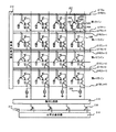
図2は、図1に示した固体撮像素子405の構成例を示す図である。固体撮像素子405は、例えばCMOS型固体撮像素子(CMOSイメージセンサ)であり、X−Yアドレス型の走査方法を採る。
FIG. 2 is a diagram illustrating a configuration example of the solid-
201は単位画素であり、フォトダイオード(PD)202、転送スイッチ203、フローティングデフュージョン部(FD)204、ソースフォロアとして機能する増幅MOSアンプ205、選択スイッチ206、及びリセットスイッチ207を有する。208は信号出力線、209は増幅MOSアンプ205の負荷となる定電流源、210は選択スイッチ、211は出力アンプである。212は垂直走査回路、213は読み出し回路、214は水平走査回路である。なお、図2においては、図の簡略化のために単位画素201を4行×4列のみ図示しているが、実際には2次元マトリクス状に非常に多数の単位画素201が配置されている。
A
単位画素201は、PD202において光を電荷に変換し、PD202で発生した電荷を転送パルスφTXに基づいて転送スイッチ203により転送してFD204に一時的に蓄積しておく。FD204、増幅MOSアンプ205、及び定電流源209でフローティングディフュージョンアンプが構成される。
The
そして、選択パルスφSELに応じて選択される選択スイッチ206で単位画素201の信号電荷が電圧に変換され、その電圧が信号出力線208を経て読み出し回路213に出力される。さらに、水平走査回路214により駆動された選択スイッチ210により出力する信号が選択され、出力アンプ211を介して撮像素子405の外部に出力される。
Then, the signal charge of the
ここで、FD204に蓄積された電荷の除去は、リセットパルスφRESにより制御されるリセットスイッチ207により行われる。また、垂直走査回路212は、転送スイッチ203、選択スイッチ206、及びリセットスイッチ207の選択を行う。すなわち、垂直走査回路212は、それらスイッチ203、206、及び207をそれぞれ制御する転送パルスφTX、選択パルスφSEL、及びリセットパルスφRESを出力する。
Here, the charge accumulated in the
なお、図2においては、パルス信号φTX、φRES、φSELのそれぞれについて、垂直走査回路212により走査選択される、例えばn番目の走査行に印加する各パルス信号を、nを添え字としてφTXn、φRESn、φSELnと記述している。後述する図4においても同様。
In FIG. 2, for each of the pulse signals φTX, φRES, and φSEL, each pulse signal applied to the nth scan row, for example, selected by the
図3は、図2に示した固体撮像素子で使用される色フィルタアレイの一部を示している。第1の色フィルタを赤(R)、第2の色フィルタを緑(G)、第3の色フィルタを緑(G)、及び第4の色フィルタを青(B)とした場合を示している。この色フィルタアレイの配列は、原色の色フィルタ配列のなかでも、特にベイヤ配列と呼ばれるものであり、高い解像度及び優れた色再現性を備えた色フィルタ配列である。 FIG. 3 shows a part of the color filter array used in the solid-state imaging device shown in FIG. The case where the first color filter is red (R), the second color filter is green (G), the third color filter is green (G), and the fourth color filter is blue (B) is shown. Yes. This array of color filter arrays is called a Bayer array among the primary color filter arrays, and is a color filter array having high resolution and excellent color reproducibility.
次に、本実施形態における固体撮像素子の動作シーケンスについて説明する。図4は、本実施形態の固体撮像素子に係るローリング電子シャッタ動作における駆動パルス及び動作シーケンスを示した図である。なお、説明を簡略にするために、図4においては、垂直走査回路212により走査選択されたn行からn+3行の4行分の駆動制御に関して図示している。
Next, an operation sequence of the solid-state image sensor in the present embodiment will be described. FIG. 4 is a diagram illustrating a driving pulse and an operation sequence in the rolling electronic shutter operation according to the solid-state imaging device of the present embodiment. In order to simplify the description, FIG. 4 illustrates drive control for four rows from n rows to n + 3 rows selected by the
固体撮像素子のn行において、まず時刻t501から時刻t502までの期間、リセットパルスφRESn及び転送パルスφTXnを印加する。これにより、転送スイッチ203及びリセットスイッチ207をオンにし、n行目の各画素201内におけるPD202及びFD204に蓄積されている不用電荷を除去するリセット動作を行う。そして、時刻t502において転送スイッチ203がオフになり、PD202で発生した光電荷が蓄積される蓄積動作が開始される。
In the n-th row of the solid-state imaging device, first, a reset pulse φRESn and a transfer pulse φTXn are applied during a period from time t501 to time t502. Accordingly, the
次に、時刻t504において、時刻t504から時刻t505までの期間、転送パルスφTXnを印加して転送スイッチ203をオンにすることで、PD202に蓄積された光電荷をFD204に転送する転送動作を行う。なお、リセットスイッチ207は、転送動作に先んじてオフする必要があり、図4に示す駆動制御では時刻t502においてn行目のリセットスイッチ207はn行目の転送スイッチ203と同時にオフとなる。ここで、リセット動作終了の時刻t502から転送動作開始の時刻t505までが、n行目における蓄積時間となる。
Next, at time t504, during the period from time t504 to time t505, a transfer pulse φTXn is applied to turn on the
n行目の転送動作終了後、選択パルスφSELnを印加して選択スイッチ206をオンにすることにより、FD204に保持した電荷が電圧に変換されて読み出し回路213に出力される。読み出し回路213で一時的に保持された信号が水平走査回路212によって時刻t506より順次出力される。
After the transfer operation of the n-th row is completed, the selection pulse φSELn is applied to turn on the
時刻t504の転送動作開始から時刻t507の読み出し動作終了までの時間をT3Readとし、時刻t501から時刻t503までの時間をT3Waitとする。
なお、他の行においても同様に駆動制御され、転送動作開始から読み出し動作終了までの時間がT3Readとなり、ある行のリセット動作開始から次の行のリセット動作開始までの間の時間がT3Waitとなる。
The time from the start of the transfer operation at time t504 to the end of the read operation at time t507 is T3Read, and the time from time t501 to time t503 is T3Wait.
The drive is similarly controlled in other rows, and the time from the start of the transfer operation to the end of the read operation is T3Read, and the time from the start of the reset operation of one row to the start of the reset operation of the next row is T3Wait. .
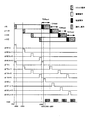
図5は、本実施形態による撮像装置における露光時間制御を概念的に示す図である。図5において、モードAは電子ズーム倍率を切替える前の撮像装置の駆動モードであり、モードBは電子ズーム倍率を切替えた後の撮像装置の駆動モードである。モードAにおける水平走査期間HDの長さはlAであり、モードBにおける水平走査期間HDの長さはlB(lB<lA)である。 FIG. 5 is a diagram conceptually showing exposure time control in the imaging apparatus according to the present embodiment. In FIG. 5, mode A is a driving mode of the imaging apparatus before switching the electronic zoom magnification, and mode B is a driving mode of the imaging apparatus after switching the electronic zoom magnification. The length of the horizontal scanning period HD in mode A is l A , and the length of the horizontal scanning period HD in mode B is l B (l B <l A ).
また、フレームN−1はモードAでの駆動期間中に撮影されたフレームであり、フレームN+1はモードBでの駆動期間中に撮影されたフレームである。フレームNは撮像装置の駆動モードがモードAからモードBに切替わる際に撮影されたフレームである。ここで、駆動モードがモードAからモードBに切替わることにより電子ズーム倍率は縮小されている。 The frame N-1 is a frame shot during the driving period in mode A, and the frame N + 1 is a frame shot during the driving period in mode B. Frame N is a frame shot when the drive mode of the imaging apparatus is switched from mode A to mode B. Here, when the drive mode is switched from mode A to mode B, the electronic zoom magnification is reduced.
時刻t101はフレームN−1における第1行目の画素の露光開始時刻であり、時刻t102はフレームN−1における第Q行目(読み出し領域の最終行目)の画素の露光開始時刻である。時刻t103はフレームN−1における第1行目の画素の読み出し開始時刻であり、時刻t104はフレームN−1における第Q行目の画素の読み出し開始時刻である。時刻t104は、撮像装置における駆動モードの切替え時刻でもある。 Time t101 is the exposure start time of the pixel in the first row in the frame N-1, and time t102 is the exposure start time of the pixel in the Qth row (the last row of the readout area) in the frame N-1. A time t103 is a reading start time of the pixel in the first row in the frame N-1, and a time t104 is a reading start time of the pixel in the Q row in the frame N-1. Time t104 is also a drive mode switching time in the imaging apparatus.
時刻t105はフレームNにおける第1行目の画素の露光開始時刻であり、時刻t106はフレームNにおける第Q行目(読み出し領域の最終行目)の画素の露光開始時刻である。時刻t107はフレームNにおける第1行目の画素の読み出し開始時刻であり、時刻t108はフレームNにおける第Q行目の画素の読み出し開始時刻である。 Time t105 is the exposure start time of the pixel in the first row in frame N, and time t106 is the exposure start time of the pixel in the Qth row (last row of the readout area) in frame N. Time t107 is the readout start time of the pixels in the first row in frame N, and time t108 is the readout start time of the pixels in the Qth row in frame N.
時刻t109はフレームN+1における第1行目の画素の露光開始時刻であり、時刻t110はフレームN+1における第R行目(読み出し領域の最終行目)の画素の露光開始時刻である。時刻t111はフレームN+1における第1行目の画素の読み出し開始時刻であり、時刻t112はフレームN+1における第R行目の画素の読み出し開始時刻である。 Time t109 is the exposure start time of the pixel in the first row in frame N + 1, and time t110 is the exposure start time of the pixel in the Rth row (the last row of the readout area) in frame N + 1. Time t111 is the readout start time of the pixels in the first row in frame N + 1, and time t112 is the readout start time of the pixels in the Rth row in frame N + 1.
フレームN−1では、時刻t101から時刻t102までの期間において第1行目から第Q行目まで1行ずつ順次露光が開始される。それぞれのラインの画素に蓄積された電荷は時刻t103から時刻t104までの期間において第1行目から第Q行目まで1行ずつ順次読み出される。このとき、各行の画素の露光期間は一定でTN-1である。 In the frame N-1, exposure is sequentially started for each row from the first row to the Qth row in the period from time t101 to time t102. The charges accumulated in the pixels of each line are sequentially read out row by row from the first row to the Q-th row in the period from time t103 to time t104. At this time, the exposure period of the pixels in each row is constant and T N−1 .
フレームN+1では、時刻t109から時刻t110までの期間において第1行目から第R行目まで1行ずつ順次露光が開始される。それぞれのラインの画素に蓄積された電荷は時刻t111から時刻t112までの期間において第1行目から第R行目まで1行ずつ順次読み出される。このとき、各行の画素の露光期間は一定でTN+1である(TN-1=TN+1)。 In the frame N + 1, exposure is sequentially started for each row from the first row to the R-th row in the period from time t109 to time t110. The charges accumulated in the pixels of each line are sequentially read out row by row from the first row to the R-th row in the period from time t111 to time t112. At this time, the exposure period of the pixels in each row is constant and T N + 1 (T N−1 = T N + 1 ).
フレームNでは、フレームN+1での各行間の露光開始時刻の時間間隔と同様の間隔で露光開始が行えるように、時刻t109から時刻t110までの間の所要期間TXから時刻t106に基づいて時刻t105を決定する。決定した時刻t105より、その所要期間TX及びフレームN+1の垂直ライン数Rから求めた時間間隔ΔT(=TX/R)で、第1行目から第Q行目まで1行ずつ順次露光が開始する。そして、それぞれのラインの画素に蓄積された電荷は時刻t107から時刻t108までの期間において第1行目から第Q行目まで1行ずつ順次読み出される。このときフレームNにおける第1行目から第Q行目までの露光期間は一定の値TNとなる。 In frame N, to allow the exposure start at the same intervals and time interval of the exposure start time of each line spacing for the frame N + 1, on the basis of the duration T X between the time point t109 to time t110 to time t106 time t105 To decide. From the determined time t105, the exposure is sequentially performed line by line from the first line to the Qth line at the time interval ΔT (= T X / R) obtained from the required period T X and the number of vertical lines R of the frame N + 1. Start. Then, the charges accumulated in the pixels of each line are sequentially read out row by row from the first row to the Q-th row in the period from time t107 to time t108. At this time, the exposure period from the first row to the Q-th row in the frame N becomes a constant value T N.
フレームNについては、さらに、全体制御演算部409が、フレームNにおける露光期間TN及びフレームN+1における露光期間TN+1の比(TN+1/TN)を算出する。そして、撮像信号処理回路406が、フレームN及びN+1における露光期間TN及びTN+1の差を補うゲインG(=TN+1/TN)を、フレームNの出力信号YN(x,y)に乗算する。これにより、露光期間TN及びTN+1の差に基づく補正が施された出力信号Y'N(x,y)(=G×YN(x,y))を得る。ここで、x、yは、フレームNにおける水平読み出し画素数をJとし、フレームNにおける垂直読み出し画素数をQとして、0≦x<J、0≦y<Qを満たす整数である。
For frame N, further, the overall
本実施形態によれば、図5に示した時刻t101から時刻t112までの間に被写体が変化しなければ、撮像装置によりフレームN−1、フレームN、及びフレームN+1ともに同じ出力を得ることができる。すなわち、電子ズーム倍率(駆動モード)の切替え時刻をまたぐフレームNにおいても、画像データに露光期間の差に係る補正を施すことで、その前後のフレームN−1、N+1における露光期間に相当するレベルの出力を得ることができる。したがって、電子ズーム倍率の切替え前後に一時的に撮影画像が明るく又は暗くなることを防止して安定した被写体輝度を得ることができ、撮影画像にちらつきが発生することを解消することができ、良好な撮影画像を得ることができる。 According to the present embodiment, if the subject does not change between time t101 and time t112 shown in FIG. 5, the same output can be obtained for the frames N-1, N, and N + 1 by the imaging device. . That is, even in the frame N that crosses the switching time of the electronic zoom magnification (driving mode), the level corresponding to the exposure period in the preceding and subsequent frames N−1 and N + 1 is obtained by performing correction related to the difference in the exposure period on the image data. Output can be obtained. Therefore, it is possible to obtain a stable subject brightness by preventing the captured image from temporarily becoming bright or dark before and after the switching of the electronic zoom magnification, and it is possible to eliminate the occurrence of flickering in the captured image. Can be obtained.
また、本実施形態による撮像装置において、駆動モードの切替え及び露出制御による蓄積期間の変更が重なった場合の駆動方法について図6に示す。 Further, FIG. 6 shows a driving method in the imaging apparatus according to the present embodiment when the change of the accumulation period by the switching of the driving mode and the exposure control is overlapped.
図6において、モードA、Bはそれぞれ電子ズーム倍率の切替え前、切替え後の駆動モードであり、モードA、Bにおける水平走査期間HDの長さはそれぞれlA、lB(lA>lB)である。また、フレームN−1、N+1は、モードA、Bでの駆動期間中にそれぞれ撮影されたフレームであり、フレームNはモードAからモードBに切替わる際に撮影されたフレームである。 In FIG. 6, modes A and B are drive modes before and after switching the electronic zoom magnification, and the lengths of the horizontal scanning periods HD in modes A and B are l A and l B (l A > l B, respectively). ). Frames N−1 and N + 1 are frames that are captured during the drive periods in modes A and B, respectively, and frame N is a frame that is captured when switching from mode A to mode B.
時刻t601、t602は、フレームN−1における第1行目、第Q行目(読み出し領域の最終行目)の画素の露光開始時刻であり、時刻t603、t604は、フレームN−1における第1行目、第Q行目の画素の読み出し開始時刻である。時刻t604は、モードAからモードBへのモード切替え時刻でもある。時刻t605、t606は、フレームNにおける第1行目、第Q行目(読み出し領域の最終行目)の画素の露光開始時刻であり、時刻t607、t608は、フレームNにおける第1行目、第Q行目の画素の読み出し開始時刻である。時刻t609、t610は、フレームN+1における第1行目、第R行目(読み出し領域の最終行目)の画素の露光開始時刻であり、時刻t611、t612は、フレームN+1における第1行目、第R行目の画素の読み出し開始時刻である。 Times t601 and t602 are exposure start times of the pixels in the first row and the Qth row (the last row of the readout region) in the frame N-1, and the times t603 and t604 are the first exposure times in the frame N-1. This is the readout start time of the pixels in the rows and Qth rows. Time t604 is also the mode switching time from mode A to mode B. Times t605 and t606 are exposure start times of the pixels in the first row and the Qth row (the last row of the readout region) in the frame N, and times t607 and t608 are the first row and the second row in the frame N. This is the readout start time of the pixels in the Qth row. Times t609 and t610 are exposure start times of the pixels in the first row and the Rth row (the last row of the readout region) in the frame N + 1, and times t611 and t612 are the first row and the second row in the frame N + 1. This is the readout start time of the pixels in the R-th row.
駆動モードの切替え及び露光期間の変更に係るそれぞれの指令が撮像装置に対して同時に与えられた場合、上述した方法と同様に、フレームNではフレームN+1での各行間の露光開始時刻の時間間隔と同様の間隔で露光開始が行えるようにする。すなわち、時刻t609から時刻t610までの間の所要期間TXから時刻t606に基づいて時刻t605を決定する。その時刻t605より、所要期間TX及びフレームN+1の垂直ライン数Rから求めた時間間隔ΔT(=TX/R)で、第1行目から第Q行目まで1行ずつ順次露光を開始する。そして、それぞれのラインの画素に蓄積された電荷は時刻t607から時刻t608までの期間において第1行目から第Q行目まで1行ずつ順次読み出される。 When the commands relating to the switching of the drive mode and the change of the exposure period are simultaneously given to the imaging apparatus, in the frame N, in the frame N, the exposure start time interval between the rows in the frame N + 1 The exposure can be started at similar intervals. That is, to determine the time t605 based on the time t606 from the required period T X between the time point t609 to time T610. From the time t605, exposure is sequentially started row by row from the first row to the Qth row at a time interval ΔT (= T X / R) obtained from the required period T X and the number of vertical lines R of the frame N + 1. . Then, the charges accumulated in the pixels of each line are sequentially read out row by row from the first row to the Q-th row in the period from time t607 to time t608.
さらに、全体制御演算部409が、フレームN、N+1におけるそれぞれの露光期間TN、TN+1の比(TN+1/TN)を算出し、撮像信号処理回路406がフレームNの出力信号YN(x,y)に露光期間の差を補うゲインG(=TN+1/TN)を乗算する。そして、露光期間の差に応じた補正が施された出力信号Y'N(x,y)(=G×YN(x,y))を得る。ここで、x、yは、フレームNにおける水平読み出し画素数をJとし、フレームNにおける垂直読み出し画素数をQとして、0≦x<J、0≦y<Qを満たす整数である。
Further, the overall
その後、フレームN+1において、第1行目の画素読み出し開始時刻t611から時刻t612において開始される読み出し動作を指定の変更量Δt(=TV)だけ遅らせる、又は早めることにより露光期間の変更を行う。このように、駆動モードの切替え対応を行った後、露光期間の変更を行うことにより、結果として全体制御演算部409が行う演算量や、全体制御演算部409に要求される必要な演算速度などの性能を抑えることができ、コスト削減効果が期待できる。
Thereafter, in the frame N + 1, the exposure period is changed by delaying or accelerating the readout operation started from the pixel readout start time t611 in the first row to the time t612 by the designated change amount Δt (= T V ). As described above, after changing the driving mode, by changing the exposure period, as a result, the amount of computation performed by the overall
なお、上述した実施形態では、モードAにおける水平走査期間HDの長さlA及びモードBにおける水平走査期間HDの長さlBは、(lA>lB)としているが、(lA<lB)の場合であっても上述した方法と同様の方法を適用することが可能である。また、上述した実施形態では、電子ズーム倍率が縮小する例を示したが、電子ズーム倍率が拡大する場合にも同様の方法を適用することが可能である。
上記では、電子ズーム動作を行う場合について記載した。しかしながら、上記に限らず、下記のようなものであっても良い。
消費電力軽減のために、連続的にフレーム画像を読み出している際に、あるフレーム画像までは、第1の期間間隔で所定ラインごとに順次リセットし、第1の期間間隔で上記所定ラインごとにフォトダイオードの信号を読み出す。そして、それ以降のフレーム画像は、第1の期間間隔と異なる第2の期間間隔で所定ラインごとに順次リセットし、第2の期間間隔で所定ラインごとにフォトダイオードの信号を読み出すように駆動を変更する。
In the above-described embodiment, the length l A of the horizontal scanning period HD in mode A and the length l B of the horizontal scanning period HD in mode B are (l A > l B ), but (l A < Even in the case of l B ), the same method as described above can be applied. In the above-described embodiment, an example in which the electronic zoom magnification is reduced has been described. However, a similar method can be applied when the electronic zoom magnification is increased.
The case where the electronic zoom operation is performed has been described above. However, the present invention is not limited to the above, and the following may be used.
In order to reduce power consumption, when continuously reading frame images, up to a certain frame image is sequentially reset for each predetermined line at a first period interval, and for each predetermined line at a first period interval. Read the photodiode signal. The subsequent frame images are sequentially reset for each predetermined line at a second period interval different from the first period interval, and are driven so as to read the photodiode signal for each predetermined line at the second period interval. change.
(本発明の他の実施形態)
上述した実施形態の機能を実現するべく各種のデバイスを動作させるように、該各種デバイスと接続された装置内のコンピュータ(CPU又はMPU)に対し、上記実施形態の機能を実現するためのプログラムを供給し、そのコンピュータに格納されたプログラムに従って上記各種デバイスを動作させることによって実施したものも、本発明の範疇に含まれる。
また、この場合、上記ソフトウェアのプログラム自体が上述した実施形態の機能を実現することになり、そのプログラム自体は本発明を構成する。また、そのプログラムをコンピュータに供給するための手段、例えばかかるプログラムを格納した記録媒体は本発明を構成する。かかるプログラムを記憶する記録媒体としては、例えばフレキシブルディスク、ハードディスク、光ディスク、光磁気ディスク、CD−ROM、磁気テープ、不揮発性のメモリカード、ROM等を用いることができる。
また、コンピュータが供給されたプログラムを実行することにより、上述の実施形態の機能が実現されるだけでなく、そのプログラムがコンピュータにおいて稼働しているOS(オペレーティングシステム)又は他のアプリケーションソフト等と共同して上述の実施形態の機能が実現される場合にもかかるプログラムは本発明の実施形態に含まれることは言うまでもない。
さらに、供給されたプログラムがコンピュータの機能拡張ボードやコンピュータに接続された機能拡張ユニットに備わるメモリに格納された後、そのプログラムの指示に基づいてその機能拡張ボードや機能拡張ユニットに備わるCPU等が実際の処理の一部または全部を行い、その処理によって上述した実施形態の機能が実現される場合にも本発明に含まれることは言うまでもない。
(Other embodiments of the present invention)
A program for realizing the functions of the above-described embodiment for a computer (CPU or MPU) in an apparatus connected to the various devices so as to operate various devices to realize the functions of the above-described embodiments. What is implemented by operating the various devices according to the program supplied and stored in the computer is also included in the scope of the present invention.
In this case, the software program itself realizes the functions of the above-described embodiments, and the program itself constitutes the present invention. Further, means for supplying the program to the computer, for example, a recording medium storing the program constitutes the present invention. As a recording medium for storing such a program, for example, a flexible disk, a hard disk, an optical disk, a magneto-optical disk, a CD-ROM, a magnetic tape, a nonvolatile memory card, a ROM, or the like can be used.
Further, by executing the program supplied by the computer, not only the functions of the above-described embodiments are realized, but the program is jointly operated with an OS (operating system) or other application software running on the computer. Needless to say, such a program is included in the embodiment of the present invention even when the functions of the above-described embodiment are realized.
Further, after the supplied program is stored in the memory provided in the function expansion board of the computer or the function expansion unit connected to the computer, the CPU or the like provided in the function expansion board or function expansion unit based on the instructions of the program Needless to say, the present invention includes the case where the functions of the above-described embodiment are realized by performing part or all of the actual processing.
なお、上記実施形態は、何れも本発明を実施するにあたっての具体化のほんの一例を示したものに過ぎず、これらによって本発明の技術的範囲が限定的に解釈されてはならないものである。すなわち、本発明はその技術思想、またはその主要な特徴から逸脱することなく、様々な形で実施することができる。 The above-described embodiments are merely examples of implementation in carrying out the present invention, and the technical scope of the present invention should not be construed as being limited thereto. That is, the present invention can be implemented in various forms without departing from the technical idea or the main features thereof.
401 レンズ部
402 レンズ駆動部
403 メカニカルシャッタ
404 メカニカルシャッタ駆動部
405 固体撮像素子
406 撮像信号処理回路
407 タイミング発生部
409 全体制御演算部
401
Claims (3)
上記撮像手段を駆動して上記画素から画像信号を読み出す駆動手段と、
上記駆動手段により上記撮像手段を第1の水平走査期間で水平走査駆動する第1の駆動モードと、上記第1の水平走査期間と長さが異なる第2の水平走査期間で水平走査駆動する第2の駆動モードとのいずれかに切替える駆動モード切替え手段と、
上記撮像手段から連続的に読み出される第1フレームの画像データと第2フレームの画像データの露光時間が異なる場合に、上記第1フレームの画像データと上記第2フレームの画像データの露光時間差を抑制するようにゲイン補正を行うゲイン補正手段と、
上記駆動モード切替え手段による駆動モードの切替え指示と露出制御による露光時間の変更指示が同時に与えられた場合に、上記駆動モード切替え手段による駆動モードの切替えを現フレームで行うように制御するとともに、上記露出制御による露光時間の変更を次フレームで行うように制御する制御手段とを有することを特徴とする撮像装置。 An imaging means in which a plurality of lines composed of a plurality of pixels are arranged;
Driving means for driving the imaging means to read out image signals from the pixels;
A first driving mode in which the image pickup means is horizontally scanned and driven by the driving means in a first horizontal scanning period, and a second driving mode in which the length is different from the first horizontal scanning period and a second horizontal scanning period that is different from the first horizontal scanning period. Drive mode switching means for switching to one of the two drive modes;
The exposure time difference between the image data of the first frame and the image data of the second frame is suppressed when the exposure time of the image data of the first frame and the image data of the second frame read out continuously from the imaging unit is different. Gain correction means for performing gain correction to
When the drive mode switching instruction by the drive mode switching means and the exposure time change instruction by exposure control are given simultaneously, the drive mode switching by the drive mode switching means is controlled to be performed in the current frame, and An imaging apparatus comprising: control means for controlling the exposure time to be changed in the next frame by exposure control.
上記駆動手段により上記撮像手段を第1の水平走査期間で水平走査駆動する第1の駆動モードと、上記第1の水平走査期間と長さが異なる第2の水平走査期間で水平走査駆動する第2の駆動モードとのいずれかに切替える駆動モード切替えステップと、
上記撮像手段から連続的に読み出される第1フレームの画像データと第2フレームの画像データの露光時間が異なる場合に、上記第1フレームの画像データと上記第2フレームの画像データの露光時間差を抑制するようにゲイン補正を行うゲイン補正ステップと、
上記駆動モード切替えステップによる駆動モードの切替え指示と露出制御による露光時間の変更指示が同時に与えられた場合に、上記駆動モード切替えステップによる駆動モードの切替えを現フレームで行うように制御するとともに、上記露出制御による露光時間の変更を次フレームで行うように制御する制御ステップとを有することを特徴とする撮像装置の制御方法。 An imaging apparatus control method comprising: an imaging unit in which a plurality of lines each including a plurality of pixels are arranged; and a driving unit that drives the imaging unit and reads an image signal from the pixel.
A first driving mode in which the image pickup means is horizontally scanned and driven by the driving means in a first horizontal scanning period, and a second driving mode in which the length is different from the first horizontal scanning period and a second horizontal scanning period that is different from the first horizontal scanning period. A drive mode switching step for switching to one of the two drive modes;
The exposure time difference between the image data of the first frame and the image data of the second frame is suppressed when the exposure time of the image data of the first frame and the image data of the second frame read out continuously from the imaging unit is different. A gain correction step for performing gain correction to
When a drive mode switching instruction by the drive mode switching step and an exposure time change instruction by exposure control are simultaneously given, control is performed so that the drive mode switching by the drive mode switching step is performed in the current frame, and And a control step for controlling the exposure time to be changed in the next frame by exposure control.
Priority Applications (1)
| Application Number | Priority Date | Filing Date | Title |
|---|---|---|---|
| JP2006049219A JP4819528B2 (en) | 2006-02-24 | 2006-02-24 | IMAGING DEVICE AND IMAGING DEVICE CONTROL METHOD |
Applications Claiming Priority (1)
| Application Number | Priority Date | Filing Date | Title |
|---|---|---|---|
| JP2006049219A JP4819528B2 (en) | 2006-02-24 | 2006-02-24 | IMAGING DEVICE AND IMAGING DEVICE CONTROL METHOD |
Publications (3)
| Publication Number | Publication Date |
|---|---|
| JP2007228433A JP2007228433A (en) | 2007-09-06 |
| JP2007228433A5 JP2007228433A5 (en) | 2009-04-09 |
| JP4819528B2 true JP4819528B2 (en) | 2011-11-24 |
Family
ID=38549765
Family Applications (1)
| Application Number | Title | Priority Date | Filing Date |
|---|---|---|---|
| JP2006049219A Expired - Fee Related JP4819528B2 (en) | 2006-02-24 | 2006-02-24 | IMAGING DEVICE AND IMAGING DEVICE CONTROL METHOD |
Country Status (1)
| Country | Link |
|---|---|
| JP (1) | JP4819528B2 (en) |
Cited By (1)
| Publication number | Priority date | Publication date | Assignee | Title |
|---|---|---|---|---|
| US11303829B2 (en) | 2019-08-28 | 2022-04-12 | Canon Kabushiki Kaisha | Imaging device and drive method of imaging device |
Families Citing this family (2)
| Publication number | Priority date | Publication date | Assignee | Title |
|---|---|---|---|---|
| JP5132497B2 (en) * | 2008-09-16 | 2013-01-30 | キヤノン株式会社 | IMAGING DEVICE AND IMAGING DEVICE CONTROL METHOD |
| DE102014020074B3 (en) | 2013-11-25 | 2022-09-01 | Canon Kabushiki Kaisha | Image pickup device and image signal control method |
Family Cites Families (4)
| Publication number | Priority date | Publication date | Assignee | Title |
|---|---|---|---|---|
| JP4503878B2 (en) * | 2001-04-27 | 2010-07-14 | オリンパス株式会社 | Imaging apparatus and imaging method |
| JP2004172845A (en) * | 2002-11-19 | 2004-06-17 | Canon Inc | Imaging device |
| JP4255345B2 (en) * | 2003-09-12 | 2009-04-15 | 株式会社ルネサステクノロジ | Imaging device |
| JP2005278060A (en) * | 2004-03-26 | 2005-10-06 | Sony Corp | Imaging signal processing apparatus, and solid-state imaging apparatus |
-
2006
- 2006-02-24 JP JP2006049219A patent/JP4819528B2/en not_active Expired - Fee Related
Cited By (1)
| Publication number | Priority date | Publication date | Assignee | Title |
|---|---|---|---|---|
| US11303829B2 (en) | 2019-08-28 | 2022-04-12 | Canon Kabushiki Kaisha | Imaging device and drive method of imaging device |
Also Published As
| Publication number | Publication date |
|---|---|
| JP2007228433A (en) | 2007-09-06 |
Similar Documents
| Publication | Publication Date | Title |
|---|---|---|
| JP4208904B2 (en) | Imaging apparatus, control method therefor, and imaging system | |
| JP4948090B2 (en) | Imaging apparatus and drive control method | |
| JP6315776B2 (en) | Imaging device, imaging device | |
| US8390692B2 (en) | Image pick up apparatus and image pick up method capable of reading signal charge for image display by newly performing exposure while reading signal charge for still image by simultaneous exposure of all pixels | |
| US9781366B2 (en) | Image sensing system and method of driving the same | |
| US11290648B2 (en) | Image capture apparatus and control method thereof | |
| JP2010130317A (en) | Image capturing apparatus, and method of controlling the same | |
| JP2002258142A (en) | Imaging apparatus | |
| JP2013183380A (en) | Image sensor, driving method for image sensor, and imaging system | |
| JP5885431B2 (en) | Imaging device and imaging apparatus | |
| US8169494B2 (en) | Image sensing apparatus and method of controlling image sensing apparatus | |
| JP4819528B2 (en) | IMAGING DEVICE AND IMAGING DEVICE CONTROL METHOD | |
| JP2010251829A (en) | Solid-state image sensor, camera system, and signal reading method | |
| JP2009124238A (en) | Imaging device and its flicker detecting method | |
| WO2021014999A1 (en) | Solid-state imaging device and method for driving same, and electronic instrument | |
| JP2005217955A (en) | Imaging device, its control method, program, and storage medium | |
| JP2020170923A (en) | Imaging element, control method of the same, and imaging apparatus | |
| US11368610B2 (en) | Image capture apparatus and control method therefor | |
| JP6393087B2 (en) | Imaging device and imaging apparatus | |
| JP4050063B2 (en) | Imaging device | |
| JP7329136B2 (en) | Imaging device | |
| WO2023162483A1 (en) | Imaging device and method for controlling same | |
| JP2004153710A (en) | Control method of imaging apparatus, and imaging apparatus | |
| JP2018170703A (en) | Imaging device, imaging apparatus, and method for controlling imaging device | |
| JP2023124783A (en) | Imaging apparatus and method for controlling the same |
Legal Events
| Date | Code | Title | Description |
|---|---|---|---|
| A521 | Request for written amendment filed |
Free format text: JAPANESE INTERMEDIATE CODE: A523 Effective date: 20090223 |
|
| A621 | Written request for application examination |
Free format text: JAPANESE INTERMEDIATE CODE: A621 Effective date: 20090223 |
|
| A977 | Report on retrieval |
Free format text: JAPANESE INTERMEDIATE CODE: A971007 Effective date: 20110524 |
|
| A131 | Notification of reasons for refusal |
Free format text: JAPANESE INTERMEDIATE CODE: A131 Effective date: 20110531 |
|
| A521 | Request for written amendment filed |
Free format text: JAPANESE INTERMEDIATE CODE: A523 Effective date: 20110726 |
|
| TRDD | Decision of grant or rejection written | ||
| A01 | Written decision to grant a patent or to grant a registration (utility model) |
Free format text: JAPANESE INTERMEDIATE CODE: A01 Effective date: 20110830 |
|
| A01 | Written decision to grant a patent or to grant a registration (utility model) |
Free format text: JAPANESE INTERMEDIATE CODE: A01 |
|
| A61 | First payment of annual fees (during grant procedure) |
Free format text: JAPANESE INTERMEDIATE CODE: A61 Effective date: 20110901 |
|
| FPAY | Renewal fee payment (event date is renewal date of database) |
Free format text: PAYMENT UNTIL: 20140909 Year of fee payment: 3 |
|
| FPAY | Renewal fee payment (event date is renewal date of database) |
Free format text: PAYMENT UNTIL: 20140909 Year of fee payment: 3 |
|
| LAPS | Cancellation because of no payment of annual fees |