JP4817423B2 - Optical interrogation system and sensor system - Google Patents
Optical interrogation system and sensor system Download PDFInfo
- Publication number
- JP4817423B2 JP4817423B2 JP2005502463A JP2005502463A JP4817423B2 JP 4817423 B2 JP4817423 B2 JP 4817423B2 JP 2005502463 A JP2005502463 A JP 2005502463A JP 2005502463 A JP2005502463 A JP 2005502463A JP 4817423 B2 JP4817423 B2 JP 4817423B2
- Authority
- JP
- Japan
- Prior art keywords
- optical
- soa
- interrogation system
- pulse
- grating
- Prior art date
- Legal status (The legal status is an assumption and is not a legal conclusion. Google has not performed a legal analysis and makes no representation as to the accuracy of the status listed.)
- Expired - Fee Related
Links
- 230000003287 optical effect Effects 0.000 title claims abstract description 491
- 238000011156 evaluation Methods 0.000 claims abstract description 29
- 238000002840 optical waveguide grating Methods 0.000 claims abstract description 26
- 239000004065 semiconductor Substances 0.000 claims abstract description 4
- 230000003321 amplification Effects 0.000 claims description 86
- 238000003199 nucleic acid amplification method Methods 0.000 claims description 86
- 230000003595 spectral effect Effects 0.000 claims description 32
- 230000005540 biological transmission Effects 0.000 claims description 10
- 238000001228 spectrum Methods 0.000 claims description 7
- 230000004044 response Effects 0.000 claims description 6
- 230000001419 dependent effect Effects 0.000 claims description 4
- 238000001514 detection method Methods 0.000 claims description 4
- 230000002269 spontaneous effect Effects 0.000 claims description 4
- 230000002457 bidirectional effect Effects 0.000 claims 7
- 230000001960 triggered effect Effects 0.000 abstract description 4
- 239000013307 optical fiber Substances 0.000 description 71
- 239000000835 fiber Substances 0.000 description 54
- 238000010586 diagram Methods 0.000 description 26
- 238000002310 reflectometry Methods 0.000 description 18
- 238000005259 measurement Methods 0.000 description 17
- 230000008901 benefit Effects 0.000 description 10
- BJQHLKABXJIVAM-UHFFFAOYSA-N bis(2-ethylhexyl) phthalate Chemical compound CCCCC(CC)COC(=O)C1=CC=CC=C1C(=O)OCC(CC)CCCC BJQHLKABXJIVAM-UHFFFAOYSA-N 0.000 description 9
- 230000008878 coupling Effects 0.000 description 7
- 238000010168 coupling process Methods 0.000 description 7
- 238000005859 coupling reaction Methods 0.000 description 7
- 238000003491 array Methods 0.000 description 6
- 238000012545 processing Methods 0.000 description 4
- 239000013078 crystal Substances 0.000 description 3
- 238000013461 design Methods 0.000 description 3
- 238000005516 engineering process Methods 0.000 description 3
- 238000000034 method Methods 0.000 description 3
- 238000012544 monitoring process Methods 0.000 description 3
- 238000000926 separation method Methods 0.000 description 3
- 239000002131 composite material Substances 0.000 description 2
- 125000004122 cyclic group Chemical group 0.000 description 2
- 230000000694 effects Effects 0.000 description 2
- 238000012806 monitoring device Methods 0.000 description 2
- 230000000737 periodic effect Effects 0.000 description 2
- 239000012466 permeate Substances 0.000 description 2
- 230000001902 propagating effect Effects 0.000 description 2
- 230000009467 reduction Effects 0.000 description 2
- 238000010521 absorption reaction Methods 0.000 description 1
- 230000004913 activation Effects 0.000 description 1
- 230000015572 biosynthetic process Effects 0.000 description 1
- 230000000903 blocking effect Effects 0.000 description 1
- 230000001351 cycling effect Effects 0.000 description 1
- 238000002839 fiber optic waveguide Methods 0.000 description 1
- 238000005286 illumination Methods 0.000 description 1
- 238000009434 installation Methods 0.000 description 1
- 238000011835 investigation Methods 0.000 description 1
- 238000004519 manufacturing process Methods 0.000 description 1
- 238000012986 modification Methods 0.000 description 1
- 230000004048 modification Effects 0.000 description 1
- 238000010079 rubber tapping Methods 0.000 description 1
- 238000003786 synthesis reaction Methods 0.000 description 1
- 230000002123 temporal effect Effects 0.000 description 1
- 238000012360 testing method Methods 0.000 description 1
- 238000012546 transfer Methods 0.000 description 1
- 230000007704 transition Effects 0.000 description 1
Images


Classifications
-
- G—PHYSICS
- G01—MEASURING; TESTING
- G01K—MEASURING TEMPERATURE; MEASURING QUANTITY OF HEAT; THERMALLY-SENSITIVE ELEMENTS NOT OTHERWISE PROVIDED FOR
- G01K11/00—Measuring temperature based upon physical or chemical changes not covered by groups G01K3/00, G01K5/00, G01K7/00 or G01K9/00
- G01K11/32—Measuring temperature based upon physical or chemical changes not covered by groups G01K3/00, G01K5/00, G01K7/00 or G01K9/00 using changes in transmittance, scattering or luminescence in optical fibres
- G01K11/3206—Measuring temperature based upon physical or chemical changes not covered by groups G01K3/00, G01K5/00, G01K7/00 or G01K9/00 using changes in transmittance, scattering or luminescence in optical fibres at discrete locations in the fibre, e.g. using Bragg scattering
-
- G—PHYSICS
- G01—MEASURING; TESTING
- G01D—MEASURING NOT SPECIALLY ADAPTED FOR A SPECIFIC VARIABLE; ARRANGEMENTS FOR MEASURING TWO OR MORE VARIABLES NOT COVERED IN A SINGLE OTHER SUBCLASS; TARIFF METERING APPARATUS; MEASURING OR TESTING NOT OTHERWISE PROVIDED FOR
- G01D5/00—Mechanical means for transferring the output of a sensing member; Means for converting the output of a sensing member to another variable where the form or nature of the sensing member does not constrain the means for converting; Transducers not specially adapted for a specific variable
- G01D5/26—Mechanical means for transferring the output of a sensing member; Means for converting the output of a sensing member to another variable where the form or nature of the sensing member does not constrain the means for converting; Transducers not specially adapted for a specific variable characterised by optical transfer means, i.e. using infrared, visible, or ultraviolet light
- G01D5/32—Mechanical means for transferring the output of a sensing member; Means for converting the output of a sensing member to another variable where the form or nature of the sensing member does not constrain the means for converting; Transducers not specially adapted for a specific variable characterised by optical transfer means, i.e. using infrared, visible, or ultraviolet light with attenuation or whole or partial obturation of beams of light
- G01D5/34—Mechanical means for transferring the output of a sensing member; Means for converting the output of a sensing member to another variable where the form or nature of the sensing member does not constrain the means for converting; Transducers not specially adapted for a specific variable characterised by optical transfer means, i.e. using infrared, visible, or ultraviolet light with attenuation or whole or partial obturation of beams of light the beams of light being detected by photocells
- G01D5/353—Mechanical means for transferring the output of a sensing member; Means for converting the output of a sensing member to another variable where the form or nature of the sensing member does not constrain the means for converting; Transducers not specially adapted for a specific variable characterised by optical transfer means, i.e. using infrared, visible, or ultraviolet light with attenuation or whole or partial obturation of beams of light the beams of light being detected by photocells influencing the transmission properties of an optical fibre
- G01D5/35383—Mechanical means for transferring the output of a sensing member; Means for converting the output of a sensing member to another variable where the form or nature of the sensing member does not constrain the means for converting; Transducers not specially adapted for a specific variable characterised by optical transfer means, i.e. using infrared, visible, or ultraviolet light with attenuation or whole or partial obturation of beams of light the beams of light being detected by photocells influencing the transmission properties of an optical fibre using multiple sensor devices using multiplexing techniques
-
- H—ELECTRICITY
- H04—ELECTRIC COMMUNICATION TECHNIQUE
- H04B—TRANSMISSION
- H04B10/00—Transmission systems employing electromagnetic waves other than radio-waves, e.g. infrared, visible or ultraviolet light, or employing corpuscular radiation, e.g. quantum communication
- H04B10/07—Arrangements for monitoring or testing transmission systems; Arrangements for fault measurement of transmission systems
- H04B10/071—Arrangements for monitoring or testing transmission systems; Arrangements for fault measurement of transmission systems using a reflected signal, e.g. using optical time domain reflectometers [OTDR]
Abstract
Description
本発明は、光インターロゲーションシステムおよびに光インターロゲーションシステムを組み込んだ光センサシステムに関する。 The present invention relates to an optical interrogation system and an optical sensor system incorporating the optical interrogation system.
多重グレーティングアレイ内でグレーティングをモニタ(interrogate)するために最も広く使われる二方法は、波長分割多重(WDM)および時分割多重(TDM)である。WDM型システムの場合、アレイ内の各グレーティングは、異なる波長窓内に位置する異なる共振波長を有するように作製される。全グレーティングを同時に照明するのに連続波広帯域光源が使用され、そして各グレーティングから得られる反射信号が、波長測定システムに現れたパワースペクトル内に同時に現れる。したがって、この波長測定システムは、多重波長を同時に測定できる必要がある。これは、光スペクトルアナライザのような走査機器は本質的な特徴であるが、波長計のような機器については問題を生じる。WDM型システムのもう一つの欠点は、アレイ内グレーティング数が増すに従って、光源の必要な操作帯域幅や波長測定システムも増えることである。 The two most widely used methods for interrogating a grating in a multiple grating array are wavelength division multiplexing (WDM) and time division multiplexing (TDM). For a WDM type system, each grating in the array is made to have a different resonant wavelength located in a different wavelength window. A continuous wave broadband light source is used to illuminate all the gratings simultaneously, and the reflected signal obtained from each grating appears simultaneously in the power spectrum appearing in the wavelength measurement system. Therefore, this wavelength measurement system needs to be able to measure multiple wavelengths simultaneously. This is an essential feature for scanning instruments such as optical spectrum analyzers, but creates problems for instruments such as wavemeters. Another drawback of WDM type systems is that as the number of gratings in the array increases, the required operating bandwidth and wavelength measurement system of the light source increases.
対照的に、TDM型システムは、通常、アレイ中の全グレーティングを同一波長窓内に位置させることができ、該グレーティングは、パルス光源で照明される。最も簡単なTDM型システムでは、ファイバの一端に発射された単一短広帯域パルスが、特定瞬間時にアレイ内特定グレーティングに到達する。グレーティングは、光パルスの一部を反射し、そして反射信号は、光源および波長測定システムへ向かってファイバを伝搬して戻る。アレイ内の他のグレーティングから反射したパルスは、異なる距離を走行しているため、異なる時間に測定システムに到着する。各グレーティングの絶対波長の相違は、光がファイバ内を約200,000,000m/秒の計算速度で走行するという事実を活用している。この種のTDM型システムを困難性は、高速操作可能な波長測定システムが必要なことである。この理由は、各反射パルスの波長を、次のパルスが到着する前に測定しなければならないからである。光速度および典型的グレーティング間隔の理由から、反射パルスは、典型的にはナノセカンドしか離隔していない。 In contrast, TDM type systems typically allow all the gratings in the array to be located within the same wavelength window, which is illuminated with a pulsed light source. In the simplest TDM-type system, a single short broadband pulse fired at one end of the fiber reaches a specific grating in the array at a specific moment. The grating reflects a portion of the light pulse, and the reflected signal propagates back through the fiber toward the light source and wavelength measurement system. Pulses reflected from other gratings in the array travel at different distances and therefore arrive at the measurement system at different times. The difference in the absolute wavelength of each grating takes advantage of the fact that light travels through the fiber at a calculated speed of approximately 200,000,000 m / sec. The difficulty with this type of TDM system is that it requires a wavelength measurement system that can be operated at high speed. This is because the wavelength of each reflected pulse must be measured before the next pulse arrives. For reasons of light speed and typical grating spacing, the reflected pulses are typically only nanoseconds apart.
別法のTDM技術は、高速波長測定に頼らずに、公知で単一波長の短光パルスを利用する。共振波長がパルスのものと一致するアレイ内グレーティングのみがパルスを反射する。パルス間の光信号の波長を変更することによって、グレーティングアレイの全スペクトルを走査し、そして、各グレーティングの波長を測定し得る。このTDM技術のもつ難点は、反射パルスを検出するための高速光ダイオード、および高速信号処理エレクトロニクスが必要なことである。走査光源、例えば同調可能レーザダイオードまたは広帯域光源、ならびに走査フィルタを持つ必要性は、これらのデバイスが、たびたび、嵩高かつ高価なのが問題である。 An alternative TDM technique utilizes short light pulses of known single wavelength without resorting to fast wavelength measurements. Only the in-array grating whose resonant wavelength matches that of the pulse will reflect the pulse. By changing the wavelength of the optical signal between pulses, the entire spectrum of the grating array can be scanned and the wavelength of each grating measured. The difficulty with this TDM technology is the need for high-speed photodiodes and high-speed signal processing electronics to detect reflected pulses. The need to have a scanning light source, such as a tunable laser diode or a broadband light source, and a scanning filter is a problem that these devices are often bulky and expensive.
これら全てのグレーティングインターロゲーションシステムが直面する問題は、高出力広帯域光源を得ることが難しいことである。広帯域源は、本来、広い波長域をカバーするので、いずれの一波長出力も通常きわめて低い(典型的には-30dB/nm)。TDM型システムでは、この問題は、長いインターパルスのもつ短パルスのみが測定システムに受け入れられ、測定システムに受け入れられる平均光出力がさらに(たびたび甚大に)減少するという事実によって強められる。 The problem faced by all these grating interrogation systems is that it is difficult to obtain a high power broadband light source. Since broadband sources inherently cover a wide wavelength range, any single wavelength output is usually very low (typically -30 dB / nm). In TDM-type systems, this problem is exacerbated by the fact that only short pulses with long interpulses are accepted by the measurement system, and the average light output accepted by the measurement system is further (and often drastically) reduced.
したがって、使用可能な出力を最大化するためには、アレイ内グレーティングの反射率を確実にきわめて大きくすることが必要である。グレーティング反射率を増大すると、測定システムで使用可能な信号が増大するが、アレイ内に存在させ得る全グレーティング数を制限するという欠点を有する。この理由は、アレイ内の各グレーティングにとって、生じたパルスは通過せねばならず、その出力のいくぶんかはグレーティングから反射して戻る際に消失するからである。パルスがより多くのグレーティングを通過すればするほど、出力はより多く消失する。さらに、グレーティングからの反射光は、測定システムに向かって伝搬して戻り、それ自身と測定システムとの間の他のグレーティングからのさらなる反射のせいで出力遅延を経験する。 Therefore, in order to maximize the usable output, it is necessary to ensure that the reflectivity of the grating in the array is very large. Increasing the grating reflectivity increases the signal available to the measurement system, but has the disadvantage of limiting the total number of gratings that can be present in the array. This is because for each grating in the array, the resulting pulse must pass and some of its output disappears upon reflection back from the grating. The more pulses that pass through the grating, the more power is lost. In addition, reflected light from the grating propagates back toward the measurement system and experiences output delay due to further reflections from other gratings between itself and the measurement system.
10%以上の反射率のグレーティングにとって、出力減少率は劇的であり得る。これは、アレイ内全グレーティング数を約5〜10へ制限し、そして、測定システムが広範囲の入力光パワーレベルに対処できなければならないことを意味する。そのうえ、TDM型センサシステム内で高反射率グレーティングを使用する欠点は、照明光パルスの多重反射の理由から著しい干渉が起こり得ることである。 For a grating with a reflectance of 10% or more, the power reduction rate can be dramatic. This means that the total number of gratings in the array is limited to about 5-10 and the measurement system must be able to handle a wide range of input optical power levels. Moreover, a drawback of using high reflectivity gratings in TDM type sensor systems is that significant interference can occur due to multiple reflections of illumination light pulses.
光インターロゲーションシステムの第二のタイプは、光パルス発信器(optical time domain reflectometer、OTDR)である。OTDRでは、光源(発光ダイオードまたはレーザダイオード)が短時間点灯して、出射光パルスを生成する。その光は、例えばテスト中の光ファイバピースに沿って走行し、そしてファイバ内のいずれかの反射点から反射される。該反射点は、一般にファイバまたは光学要素、例えばパッチコードコネクタ内の破断部である。一般的なファイバ後方散乱の理由から、反射がまた生起するかもしれない。反射信号は、連続パルスとして検出器に記録される。アウトバウンド光パルスに対する反射パルスのタイミングは、ファイバに沿った破断部またはコンポーネントの位置を決定する。反射光信号の大きさは、反射点の種類に依存し、例えば平滑なパッチコードコネクタからの反射は約4%であり、一方、破断ファイバからの反射量はこれ以下である。 The second type of optical interrogation system is an optical time domain reflectometer (OTDR). In OTDR, a light source (light emitting diode or laser diode) is turned on for a short time to generate an emitted light pulse. The light travels, for example, along the optical fiber piece under test and is reflected from any reflection point in the fiber. The reflection point is generally a break in a fiber or optical element, such as a patch cord connector. Reflections may also occur for general fiber backscatter reasons. The reflected signal is recorded on the detector as a continuous pulse. The timing of the reflected pulse relative to the outbound light pulse determines the position of the break or component along the fiber. The magnitude of the reflected light signal depends on the type of reflection point, for example, the reflection from a smooth patch cord connector is about 4%, while the amount of reflection from a broken fiber is less than this.
既存のOTDR技術に付随する主な問題は、異なる反射パルスの到着時間を区別するためにきわめて高速の信号処理エレクトロニクスが必要なことである。高速エレクトロニクスを使用することは、反射パルス量の測定精度が低いことを意味する。さらに、反射光信号は一般に、低光出力であり、低SN比を生じる。 The main problem associated with existing OTDR technology is that very fast signal processing electronics are required to distinguish the arrival times of the different reflected pulses. Using high-speed electronics means that the measurement accuracy of the reflected pulse amount is low. Furthermore, the reflected light signal generally has a low light output and produces a low signal-to-noise ratio.
本発明の第一の様相によれば、光パルスを生成するように動作可能な光源であって、他端にて一以上のモニタされる反射光学素子に光結合した光導波路の一端に結合される該光源と、
該導波路に光結合し、モニタ中の反射光学素子から帰還する光パルスを選択的に透過し、さらに透過された光信号を光増幅するように動作可能な光増幅およびゲート手段(optical amplifying and gating means)と、
該光増幅およびゲート手段に光結合し、該光増幅およびゲート手段によって透過された帰還光パルスを検知するように動作可能な光学検知手段と
を含む光インターロゲーションシステムを提供する。
According to a first aspect of the invention, a light source operable to generate an optical pulse is coupled at one end of an optical waveguide optically coupled to one or more reflective optical elements to be monitored at the other end. The light source;
Optical amplifying and gating means optically coupled to the waveguide, selectively transmitting optical pulses returning from a reflective optical element in the monitor, and operable to optically amplify the transmitted optical signal. gating means),
An optical interrogation system is provided that includes optical sensing means optically coupled to the optical amplification and gating means and operable to sense feedback light pulses transmitted by the optical amplification and gating means.
光増幅およびゲート手段は、好ましくはスイッチ型操作可能な光増幅素子であり、該光増幅およびゲート手段をスイッチオンしたときに光信号を透過かつ増幅し、スイッチオフしたときに光信号の透過および増幅を回避する。該光増幅およびゲート手段は、好ましくは双方向(bi-directionally)に動作可能であり、より好ましくは、利得クランプする半導体光増幅器を含む。インターロゲーションシステムは、好ましくはさらに光増幅およびゲート手段用の駆動装置を含み、該駆動装置は光増幅およびゲート手段にスイッチオン・オフさせるように動作可能である。 The optical amplification and gate means is preferably a switch-type operable optical amplification element, which transmits and amplifies the optical signal when the optical amplification and gate means is switched on, and transmits and amplifies the optical signal when the switch is turned off. Avoid amplification. The optical amplification and gating means is preferably bi-directionally operable and more preferably includes a gain-clamping semiconductor optical amplifier. The interrogation system preferably further comprises a drive for optical amplification and gating means, which is operable to switch on and off the light amplification and gating means.
該駆動装置は、好ましくは可変周波数および継続時間をもつ電気駆動パルスを生成するように動作可能である。該駆動装置は、電気駆動パルス対を生成してよい。該駆動装置は、別法として、電気駆動パルス対のストリームを生成してもよい。該駆動装置は、さらに別法として、電気駆動パルスの連続ストリームを、選択周波数においてかつそれぞれが同一の継続時間を有するように生成してよい。電気駆動パルスは、好ましくは、光信号が最も隣接した反射光学素子間を走行するのに必要な時間の二倍よりも短い。 The drive is preferably operable to generate an electrical drive pulse with a variable frequency and duration. The driver may generate an electric drive pulse pair. The drive may alternatively generate a stream of electrical drive pulse pairs. The drive may alternatively generate a continuous stream of electrical drive pulses at a selected frequency and each having the same duration. The electrical drive pulse is preferably less than twice the time required for the optical signal to travel between the nearest reflective optical elements.
該駆動装置は、可変周波数発信器によってトリガされる電気パルス発生器を含んでよく、あるいは別法として、デジタル可変電気パルス発生装置を含んでよい。 The drive may include an electrical pulse generator that is triggered by a variable frequency oscillator, or alternatively may include a digital variable electrical pulse generator.
複数の光増幅およびゲート手段を設けてよく、個々の光導波路に光結合される各手段が、モニタされる反射光学素子を一以上含んでいる。好ましくは、各光増幅およびゲート手段は、単一駆動装置により制御され、該駆動装置は、モニタされる選択された反射光学素子を含む光導波路の個々の光増幅およびゲート手段に選択的に結合可能である。 A plurality of optical amplification and gate means may be provided, each means optically coupled to an individual optical waveguide including one or more reflective optical elements to be monitored. Preferably, each optical amplification and gating means is controlled by a single drive, which is selectively coupled to the individual optical amplification and gating means of the optical waveguide containing the selected reflective optical element to be monitored. Is possible.
該光源は、好ましくは光増幅およびゲート手段がスイッチオンされると同時に、増幅自然放出光信号を生成し、そして該光信号を光パルス中へゲート制御する光増幅およびゲート手段を含む。該光源は、付随的に光増幅およびゲート手段と光導波路との間に設ける光フィルタを含んでもよい。 The light source preferably includes optical amplification and gating means that generates an amplified spontaneous emission optical signal and gates the optical signal into an optical pulse at the same time as the optical amplification and gating means is switched on. The light source may additionally include an optical filter provided between the optical amplification and gate means and the optical waveguide.
該光源は、別法として、連続波光信号を生成するように動作可能であり、光増幅およびゲート手段に結合する連続波光源を含んでもよく、光増幅およびゲート手段がスイッチオン・オフする際、連続波光信号が光パルス中へゲート制御する。連続波光源は、スーパールミネッセント光ダイオードであり得る。光源は、付随的に連続波光源と光増幅およびゲート手段との間、または光増幅およびゲート手段と光導波路との間に設ける光フィルタを含んでもよい。 The light source is alternatively operable to generate a continuous wave optical signal and may include a continuous wave light source coupled to the optical amplification and gating means, when the optical amplification and gating means switches on and off. A continuous wave optical signal gates into the optical pulse. The continuous wave light source can be a superluminescent photodiode. The light source may additionally include an optical filter provided between the continuous wave light source and the optical amplification and gate means, or between the optical amplification and gate means and the optical waveguide.
該光源は、さらに別法として、光パルスを生成するように動作可能なパルス光源を含んでもよい。該光源は、付随的に、パルス光源の後に設けられる光フィルタを含んでよい。該インターロゲーションシステムは、好ましくは、さらに光パルスを光導波路に結合するための光結合手段を含む。該光結合手段は、光導波路ルーティングデバイス、例えば光導波路結合器を含んでよく、あるいは、別法として、光スイッチデバイスを含んでよい。 The light source may further alternatively include a pulsed light source operable to generate a light pulse. The light source may additionally include an optical filter provided after the pulsed light source. The interrogation system preferably further includes optical coupling means for coupling the optical pulse to the optical waveguide. The optical coupling means may include an optical waveguide routing device, such as an optical waveguide coupler, or alternatively, an optical switch device.
光フィルタは、好ましくはモニタされる一以上の反射光学要素によって占められるスペクトル帯域に実質的に一致する透過プロファイルを有し、こうして波長へ作用する該光フィルタは、パルスの光学帯域幅を制限する。 The optical filter preferably has a transmission profile that substantially matches the spectral band occupied by the one or more reflective optical elements to be monitored, so that the optical filter acting on the wavelength limits the optical bandwidth of the pulse. .
モニタされる反射光学素子が二以上の異なる光導波路に結合する場合、光源が各光導波路のために設けられてよい。別法として、単一光源を使用し、該光源を光ルーティング素子、例えば光導波路結合器または光スイッチを介して光導波路と結合してよい。 If the reflective optical element to be monitored is coupled to two or more different optical waveguides, a light source may be provided for each optical waveguide. Alternatively, a single light source may be used and coupled to the optical waveguide via an optical routing element, such as an optical waveguide coupler or optical switch.
光学検知手段は、光検出器を含み得る。該光学検知手段は、別法として光増幅およびゲート手段に光結合した波長評価装置を含み得、これは、光増幅およびゲート手段によって透過された帰還光パルスの波長を評価するように動作可能である。 The optical sensing means may include a photodetector. The optical sensing means may alternatively comprise a wavelength evaluation device optically coupled to the optical amplification and gating means, which is operable to evaluate the wavelength of the feedback light pulse transmitted by the optical amplification and gating means. is there.
該波長評価装置は、波長依存性のフィルタ応答を有する光フィルタ素子を含み、それは光学検知手段、例えば光検出器を従え、該光学検知手段からの電気出力は、検出光信号の波長を決定するように動作可能な単一の処理手段によって処理され、光増幅およびゲート手段のゲート制御は、それがどのグレーティングから帰還したのかを同定し、そして、濾波された光信号の光出力は、その波長を同定する。該光フィルタ素子は、バルクオプティック光フィルタを含み得る。光フィルタは、別法として、光導波路グレーティング、例えばグレーティングのスペクトルプロファイルにわたって波長とともに実質的に線形に変化する反射率を有するチャープトブラッググレーティング、あるいは、グレーティングのスペクトルプロファイルにわたって波長とともに変化する結合係数を有する傾斜光導波路グレーティングを含み得る。 The wavelength evaluation device includes an optical filter element having a wavelength dependent filter response, which is accompanied by optical sensing means, for example a photodetector, and the electrical output from the optical sensing means determines the wavelength of the detected optical signal. Processed by a single processing means operable so that the optical amplification and gating control of the gating means identify from which grating it has returned, and the optical output of the filtered optical signal is at its wavelength Is identified. The optical filter element may include a bulk optic optical filter. An optical filter may alternatively have an optical waveguide grating, for example a chirped Bragg grating having a reflectivity that varies substantially linearly with wavelength over the spectral profile of the grating, or a coupling coefficient that varies with wavelength over the spectral profile of the grating. An inclined optical waveguide grating can be included.
波長評価装置は、別法として、波長計または光スペクトルアナライザを含み得、光増幅およびゲート手段のゲート制御は、どの反射光学素子から光信号が帰還したかを同定し、そして波長計または光スペクトルアナライザは、光信号の波長を測定する。 The wavelength evaluation device may alternatively include a wavemeter or optical spectrum analyzer, wherein the optical amplification and gating control of the gate means identifies from which reflective optical element the optical signal is fed back, and the wavemeter or optical spectrum. The analyzer measures the wavelength of the optical signal.
インターロゲーションシステムは、さらに光増幅およびゲート手段と、一以上のモニタされる反射光学素子を含む個々の光導波路との間に結合する光導波路セクションを含み得る。 The interrogation system may further include an optical waveguide section coupled between the optical amplification and gating means and individual optical waveguides including one or more monitored reflective optical elements.
インターロゲーションシステムは、別法としてまたは付随的に、光増幅およびゲート手段を通ってモニタされる反射光学素子から帰還する光パルスを、モニタ中の反射光学素子に向かってルーティングするように設計された光信号ルーティング手段を含み得る。 The interrogation system is alternatively or additionally designed to route light pulses returning from the reflective optical element monitored through the optical amplification and gating means toward the reflective optical element being monitored. Optical signal routing means.
光信号ルーティング手段があると、モニタされる反射光学素子から反射してきた光パルスに、光増幅およびゲート手段を通って反射して戻らせ、光導波路中へ反射して戻らせ、モニタされる反射光学素子へ反射して戻らせる(それは再反射する)ことなどができる。このようにして、該光パルスは、モニタ中の反射光学素子から前後に循環する際に、その都度光増幅およびゲート手段を通過して多重増幅を経験する。光信号ルーティング手段は、好ましくは光増幅およびゲート手段の後に設けられた光反射器を含み、光信号が光増幅およびゲート手段から反射器へ伝搬し、そして光増幅およびゲート手段へ戻るのに要する時間ならびに光増幅およびゲート手段をスイッチオンする電気駆動パルスの継続時間よりも確実に短くなるように、該反射器は光増幅およびゲート手段に十分近くに位置する。 With optical signal routing means, light pulses reflected from the reflective optical element to be monitored are reflected back through the optical amplification and gate means, reflected back into the optical waveguide, and monitored reflection It can be reflected back to the optical element (it re-reflects) and so on. In this way, each time the light pulse circulates back and forth from the reflective optical element being monitored, it passes through the light amplification and gate means and experiences multiple amplification. The optical signal routing means preferably comprises an optical reflector provided after the optical amplification and gating means, which is required for the optical signal to propagate from the optical amplification and gating means to the reflector and back to the optical amplification and gating means The reflector is located sufficiently close to the optical amplification and gating means to ensure that it is shorter than the time and duration of the electrical drive pulse that switches on the optical amplification and gating means.
該光反射器の反射におけるスペクトルプロファイルは、好ましくは一以上のモニタされる反射光学素子によって占められるものと同一のスペクトル帯域をカバーする。該光反射器は、100パーセントより小さい反射率を有してよく、これにより、光信号の一部を透過して、その後、波長評価装置へルーティングされる。該光反射器は、光信号タッピング素子(tapping element)、例えば光導波路結合器と結合してよく、これにより、該光反射器に100パーセントの反射率を持たせ、光反射器から反射する光信号の一部は、タップオフ(tapped off)され、そして該波長評価装置へルーティングされる。 The spectral profile in the reflection of the light reflector preferably covers the same spectral band occupied by one or more monitored reflective optical elements. The light reflector may have a reflectivity of less than 100 percent, whereby a portion of the optical signal is transmitted and then routed to the wavelength estimator. The light reflector may be coupled to an optical signal tapping element, such as an optical waveguide coupler, thereby providing the light reflector with 100% reflectivity and reflecting light from the light reflector. Part of the signal is tapped off and routed to the wavelength estimator.
インターロゲーションシステムは、別法としてさらに、光増幅およびゲート手段の後に設けた一連の光反射器を含み得、光信号が光増幅およびゲート手段から最遠方の反射器に伝搬し、そして光増幅およびゲート手段へ戻るのに要する時間が、光増幅およびゲート手段をスイッチオンする電気駆動パルスの継続時間より確実に短くなるように、各反射器は、光増幅およびゲート手段から異なる距離に位置し、最も遠方の反射器は、光増幅およびゲート手段に充分近くに位置する。各光反射器の反射におけるスペクトルプロファイルは、好ましくは異なるスペクトル帯域をカバーする。 The interrogation system may alternatively further comprise a series of optical reflectors provided after the optical amplification and gating means, wherein the optical signal propagates from the optical amplification and gating means to the farthest reflector, and the optical amplification And each reflector is located at a different distance from the optical amplification and gate means to ensure that the time required to return to the gate means is less than the duration of the electrical drive pulse that switches on the optical amplification and gate means. The farthest reflector is located sufficiently close to the optical amplification and gating means. The spectral profile in the reflection of each light reflector preferably covers a different spectral band.
該光反射器または各反射器は、好ましくは光導波路グレーティングであり、そして最も好ましくはブラッググレーティングである。 The light reflector or each reflector is preferably an optical waveguide grating and most preferably a Bragg grating.
該光信号ルーティング手段は、別法として、光パルスが光増幅およびゲート手段を通って一方向のみに走行し、一以上の反射光学素子に向かうように、一以上の反射光学素子に結合した光導波路と光増幅およびゲート手段との間に延在しかつ光結合し得る。 The optical signal routing means may alternatively be an optical signal coupled to one or more reflective optical elements so that the optical pulse travels in only one direction through the optical amplification and gating means and is directed to the one or more reflective optical elements. It may extend between the waveguide and the optical amplification and gating means and be optically coupled.
インターロゲーションシステムは、波長評価装置の前(光信号によって見られるような)に設けた光フィルタを含み、該光フィルタは、一以上のモニタされる反射光学素子によって占められるスペクトル帯域と実質的に一致する透過プロファイルを有し、これにより光フィルタは、一以上の反射光学素子のスペクトル帯域をはずれた波長の帰還光信号のどの部分も実質的に除去するように作用する。 The interrogation system includes an optical filter provided in front of the wavelength estimator (as seen by the optical signal), which is substantially the spectral band occupied by the one or more monitored reflective optical elements. So that the optical filter acts to substantially remove any portion of the return optical signal having a wavelength outside the spectral band of the one or more reflective optical elements.
該光導波路または各光導波路は、光ファイバまたは平面光導波路であり得る。 The optical waveguide or each optical waveguide may be an optical fiber or a planar optical waveguide.
本発明の第二の様相によれば、一端を一以上の反射光学素子に結合した光導波路を含み、該光導波路は、他端を本発明の第一の様相の光インターロゲーションシステムに結合させる光センサシステムを提供する。 According to a second aspect of the present invention, an optical waveguide comprising one end coupled to one or more reflective optical elements, the other end coupled to the optical interrogation system of the first aspect of the present invention. An optical sensor system is provided.
光センサシステムは、好ましくは、光導波路グレーティングの離隔したアレイに結合した光導波路を含む。アレイ内各グレーティングの共振波長は、好ましくは同一波長窓内にあり、これにより全グレーティングが単一光チャンネル内で作動する。 The optical sensor system preferably includes an optical waveguide coupled to a spaced array of optical waveguide gratings. The resonant wavelength of each grating in the array is preferably in the same wavelength window, so that all the gratings operate in a single optical channel.
別法として、アレイ内グレーティングは、グループごとに配置されてもよく、各グループは、実質的に同一のグレーティングセットを含み、モニタされるグレーティングがどのグループに属するのかを帰還光パルスの飛行時間が同定できるように、一グループ内の各グレーティングの共振波長が、異なる波長窓内に存在して、異なる光チャンネル内で作動する。 Alternatively, the in-array gratings may be arranged in groups, each group containing substantially the same set of gratings, and the time of flight of the return light pulse to determine which group the grating being monitored belongs to. As can be identified, the resonant wavelength of each grating in a group exists in a different wavelength window and operates in a different optical channel.
該センサシステムは、複数の光導波路を含み得、それぞれは、光導波路グレーティングの離隔したアレイを含み、各導波路は、個々の光増幅およびゲート手段に結合している。 The sensor system may include a plurality of optical waveguides, each including a spaced array of optical waveguide gratings, each waveguide coupled to an individual optical amplification and gating means.
該光導波路または各光導波路は、光ファイバまたは平面光導波路であり得る。アレイ光導波路グレーティングは、好ましくはブラッググレーティングである。 The optical waveguide or each optical waveguide may be an optical fiber or a planar optical waveguide. The array optical waveguide grating is preferably a Bragg grating.
該反射光学素子または各反射光学素子は、別法として、バルクオプティックファブリー−ペローエタロンであり得るファブリー−ペローエタロンデバイス、光ファイバファブリー−ペローエタロン、または光導波路グレーティングをベースとするファブリー−ペローエタロンでよい。該反射光学素子または各反射光学素子は、別法として、さらに、終端が鏡面であり得る光ファイバの端部、光ファイバパッチコードの端部、光ファイバの一セクション内の破断部、結晶をベースとする反射光学素子、またはミラー部材であり得る。 The reflective optical element or each reflective optical element may alternatively be a Fabry-Perot etalon device, which may be a bulk optic Fabry-Perot etalon, an optical fiber Fabry-Perot etalon, or a Fabry-Perot etalon based on an optical waveguide grating. Good. The reflective optical element or each reflective optical element may alternatively be further based on an end of an optical fiber whose end may be a mirror surface, an end of an optical fiber patch cord, a break in a section of optical fiber, a crystal Or a mirror member.
本発明の特別な実施態様を、添付の図面を(事例としてのみに)用いて以下に詳細に説明する。 Specific embodiments of the present invention are described in detail below using the accompanying drawings (for example only).
本発明の第1の実施態様は、図1(a)に示すように、光インターロゲーションシステム10を提供する。該インターロゲーションシステム10は、モニタされる反射光学素子(この実施例では、グレーティングG)の入った光導波路16に結合する光パルスを生成するように動作可能な光源12、14を備える。該インターロゲーションシステム10は、さらに光増幅およびゲート手段を備え、それはこの実施例では、双方向に動作可能な半導体光増幅器(SOA)14の形態をとる。SOA14は、モニタされるグレーティングの入った導波路16と光結合する。インターロゲーションシステム10は、また、光学検知手段を備え、この実施例ではSOA14と光結合した波長計18の形態をとる。該波長計18は、SOA14によって透過された帰還光パルスの波長を評価するように動作可能である。
The first embodiment of the present invention provides an
この実施例では、該光源は、スーパールミネッセントダイオード(SLD)12の形態の連続波(CW)光源を備え、SOA14によって光パルスへゲート制御される。SLD12の出力は、信号分割デバイス(この実施例では、光ファイバ結合器20であるが、別法としてサーキュレータであり得る)のポートAおよびBを介してSOA14へ結合される。
In this embodiment, the light source comprises a continuous wave (CW) light source in the form of a superluminescent diode (SLD) 12 and is gated into light pulses by
インターロゲーションシステム10は、さらに、SOA14にスイッチオン・オフさせるように動作可能な駆動手段22を備える。SOAは、通常、単一または多重チャンネル遠隔通信ネットワーク内の増幅器としてもっぱら使用され、そこでは、「連続オン」モードで操作され、DC電気駆動信号によって駆動される。本発明では、SOA14は、パルス駆動モードで操作され、そしてナノ秒時間で作動する必要がある。
The
駆動手段22は、SOA14に適用される電気駆動パルス(挿入図(a)参照)を生成する。この実施例では、駆動手段22は、該可変周波数発信器(図示せず)によってトリガされる電気パルス発生器を備える。可変周波数発信器は、直接デジタル波形合成(DDS)、または周波数シンセサイザ集積回路を用いて構築され、その周波数選択は、マイクロプロセッサの制御のもとでデジタル的に履行される。該パルス発生器は、アナログまたはデジタル遅延線路、簡単なRCタイミング回路、または論理ゲートディレイで構築してもよい。
The drive means 22 generates an electric drive pulse (see inset (a)) applied to the
駆動手段22は、別法として、可変周波数発信器、遅延発生器、およびパルス発生器の機能をデジタル履行するように動作可能な単一のプログラマブルデバイスを含んでもよい。適当なデジタルプログラマブル駆動手段22を図1(b)に示す。周波数、継続時間、およびパルスの遅延は、水晶精度で制御される。典型的クロック周波数200MHzの場合、少なくとも5nsの時間分解能が可能である。多重フェーズクロッキングを採用するより進んだ設計では、時間分解能がさらに一層増大する。 The drive means 22 may alternatively include a single programmable device operable to digitally perform the functions of a variable frequency oscillator, a delay generator, and a pulse generator. A suitable digital programmable drive means 22 is shown in FIG. 1 (b). Frequency, duration, and pulse delay are controlled with crystal accuracy. For a typical clock frequency of 200 MHz, a time resolution of at least 5 ns is possible. More advanced designs that employ multiple phase clocking will further increase temporal resolution.
電気駆動パルスをSOA14へ適用すると、SOA14がスイッチオンし、入射光信号をSOA14で透過および増幅することが可能になる。電力がSOA14にかけられていないときは、SOA14はスイッチオフし、高い分光吸収を有して、実質的に入射光信号の透過を妨害する。SOA24は、これにより、光信号、特にモニタ中のグレーティングGから帰還した光パルスを選択的に透過する。
When an electrical drive pulse is applied to the
一連の電気駆動パルス(この実施例では、一連の駆動パルス対)をSOA14へ適用することによって、SLD12からのCW光信号は、一連の光パルスにゲート制御される。該光信号はSOA14中を伝搬する際、光増幅を受ける。光パルス(標準単一モード光ファイバ導波路について)の概算の空間長さ(spatial length)は、〜0.2m/nsであるように選択される。
By applying a series of electrical drive pulses (in this embodiment, a series of drive pulse pairs) to the
一以上の反射光学素子をモニタするために、インターロゲーションシステム10は、一以上のモニタされる反射光学素子の入った光導波路に結合される。この実施例ではインターロゲーションシステム10は、ファイバブラッググレーティング(G1〜Gn)のアレイが組み込まれたセンシングセクション24を含む光ファイバ16に結合される。インターロゲーションシステム10およびグレーティングアレイは、一緒になって本発明の第2の実施態様に従う光センサシステム26を形成し、アレイ内各グレーティングGは、センサ素子を形成する。各グレーティングGの共振波長は、この実施例では実質的に同一であり、したがって、各グレーティングGは、同一光チャンネル内で作動する。この実施例では、グレーティングGの長さは2.5mmであり、そして共振波長1550nm、スペクトル帯域幅0.2nm、および透過損失4%を有する。図1(a)に示す4個のグレーティングは、n個のグレーティングを示す意図であり、nは最高1000であり得る。
In order to monitor one or more reflective optical elements,
光導波路グレーティング、特に光ファイバブラッググレーティングのセンサとしての使用は、当業者には周知であるので、その操作および用途は、ここで詳細に説明しない。 Since the use of optical waveguide gratings, particularly optical fiber Bragg gratings, as sensors is well known to those skilled in the art, their operation and application will not be described in detail here.
操作において、第一の電気駆動パルスをSOA14へ適用すると、第一の光パルスが生成し、ファイバ16内に結合される。光パルスは、ファイバ16に沿って伝搬しし、アレイ内各グレーティングGと順番に出会い、そして、パルスの一部は各グレーティングによって反射される。入射光パルスの空間長さが、アレイ内グレーティング間の最小空間距離の二倍以下である限り、その結果は一連の反射光パルスになり、それぞれもとの光パルスと同一長さであるが、個々のグレーティングGからの各反射光パルスの全伝搬時間の差に従って時間および空間的に分離している。したがって、SOA14に向かって伝搬して戻る反射光パルスは、異なる時間にSOA14に到着する。したがって、各反射光パルスの飛行時間は、そこから反射したグレーティングを同定する。
In operation, when a first electrical drive pulse is applied to the
当業者に理解されるのは、CW光源,SLD12は、パルス光源によって置換し得ることである。電気駆動パルスのSOA14に対するタイミングは、パルス光源によって生成され光パルスの選択された一つが光ファイバ16中へ放出されるように微調整される。
It will be understood by those skilled in the art that the CW light source,
モニタのための特定の反射光学素子の選択(この実施例では、モニタ用グレーティングG)は、電気駆動パルス間の時間周期T1を調整することにより達成する。電気駆動パルスの周波数は、各対内の第一パルスおよび第二パルス間の期間T1が、SOA14からの第一駆動パルスの結果として生成される光パルスが選択されたグレーティングG1(図1(a))へ行って矢28に示すように戻るまでの飛行時間と等しくなるように設定される。したがって、SOA14は、反射光パルス(グレーティングG1由来)がSOA14に帰着するときに、駆動手段22からの第二の電気駆動パルスを受ける。結果として、SOA14は、反射パルスが到着するときにスイッチオンされ、反射パルスを、SOA14を通って透過させることができ、反射したパルスは同時に増幅される。SOA14がスイッチオンされる前後に到着する、すなわち、アレイ内の別のグレーティングに由来するいずれの反射光パルスも吸収され、したがって透過されない。光パルスの継続時間は、アレイ内の最も近接したグレーティングの光パルスの飛行時間の二倍より短くなるように選択される。
(In this example, a monitor grating G) Selection of the particular reflecting optical element for the monitor is achieved by adjusting the time period T 1 of the between electrical drive pulses. The frequency of the electric drive pulse is such that the period T 1 between the first pulse and the second pulse in each pair is a grating G 1 in which an optical pulse generated as a result of the first drive pulse from the
ゲート制御された反射光パルスは、次いで、SOA14から波長計18へ、結合器20のポートBおよびCを介してルーティングされ、そこで、反射した光パルスの波長、そしてモニタされるグレーティングG1の波長が、測定および記録される。
The gated reflected light pulse is then routed from
第二の電気駆動パルスをSOA14に適用すると、反射光パルスのゲート制御に加えてもう一つの効果が得られ、すなわち、第二の光パルスが生成して、光ファイバ16中に結合される。
Applying the second electrical drive pulse to the
二電気駆動パルスのみをSOA14の駆動に使用する場合、上記したように、一反射光パルスのみが波長測定システムに帰着する。これは単独でも有用であるが、単一パルスから測定できる迅速な測定システムが必要となる。別法として、一連の電気駆動パルスを使用する。第二電気駆動パルスによってSOA14に対して生成される第二の光パルスが、グレーティングによって反射され、そしてSOA14によって吸収されるのを許容し、それによりそれがシステムから除去され、後続の光パルスとの干渉を回避するために、駆動パルス対間に充分な時間を許容しなければならない。
When only two electrical drive pulses are used to drive the
本発明の第3の実施態様に従う光インターロゲーションシステム30を図2に示す。インターロゲーションシステム30は、本発明の第1の実施態様に従うインターロゲーションシステム10と実質的に同一であるが、以下が変更されている。同一の参照番号は、対応の特徴を維持する。
An
この実施例では、駆動手段22は、挿入図(a)に示すような一連の電気駆動パルスを生成するように動作可能である。各電気駆動パルスは、同一の継続時間をもち、そして、パルス間の周期は一定である。電気駆動パルスの継続時間は、光信号がアレイ内の最も近接する反射光学素子グレーティングG間を伝搬するのに必要とする時間の二倍より長くならないよう選択される。可変周波数発信器の周波数、およびそれゆえ電気駆動パルスの周波数は、モニタされるアレイ内特定グレーティングを選択するように変更される。可変周波数発信器の周波数は、電気駆動パルス間の周期T1が、SOA14からの光パルスが選択したグレーティング(この実施例ではG1)に行き、そしてSOA14へ戻る飛行時間と等しくなるように選択される。概略図は、SOA14と選択したグレーティング(標準の光ファイバと仮定)との間の光ファイバの各mに対して10nsである。
In this embodiment, the drive means 22 is operable to generate a series of electrical drive pulses as shown in inset (a). Each electrical drive pulse has the same duration and the period between the pulses is constant. The duration of the electrical drive pulse is selected so that it does not exceed twice the time required for the optical signal to propagate between the closest reflective optical element gratings G in the array. The frequency of the variable frequency oscillator, and hence the frequency of the electrical drive pulse, is changed to select the specific grating in the array to be monitored. Frequency of the variable frequency oscillator, the period T 1 of the between electrical drive pulses, selected to go to, and equal to the flight time back to the SOA 14 (G 1 in this embodiment) grating light pulse is selected from the
駆動手段22の制御のもとでは、したがって、SOA14は、規則正しいインターバルでスイッチオン・オフされる。SOA14がスイッチオンされるたびに、光パルスが生成され、そして光ファイバ16中に放出され、同時に正確な反射光パルスをゲート制御し、次いで上記したように、波長計18へ伝搬する。
Under the control of the drive means 22, the
より重要なことは、光導波路の追加のセクション、この実施例では、SOA14の後(すなわち、使用中)で、SOA14とモニタされる反射光学素子(グレーティングG)の入った光ファイバ16との間に、ある長さの光ファイバ32を含めることである。この追加長の光ファイバ32は、一以上のグレーティングGからの反射光パルスのSOA14での同時受信に由来する干渉の可能性を除去するために含められる。この理由を理解するために、追加のファイバ32が存在しないで、インターロゲーションシステム30が、SOA14から1mの間隔をもって空いている3個のグレーティング(G1-3)が入った光ファイバに結合した図3に示す状況を検討する。もし、例えば、インターロゲーションシステム30が、SOA14から1mの位置にある第一グレーティングG1の波長をモニタするように設定されたら、以下の事象が起きるであろう。
More importantly, an additional section of the optical waveguide, in this example, after SOA 14 (ie in use), between
時間T0にて、第一電気駆動パルスがSOA14に適用され、光パルスAが生成され、そしてファイバ16に放出され、そこでパルスはグレーティングGに向かって透過する。その後、時間Ts(Ts=5nsの場合、それは光信号が標準の光ファイバを1m走行するのに要する時間である)にて、光パルスAの一部は、第一グレーティングG1から反射し、この第一の反射したパルスαは、SOA14に向かって伝搬して戻る。光パルスAの残余は、第二および第三のグレーティングG2およびG3に引き続き向かう。
At time T 0 , a first electrical drive pulse is applied to the
時間2Tsにて、第二の電気駆動パルスがSOA14に適用され、第二の光パルスBを生成させ、そしてファイバ16に向かって放出され、そこでパルスは、また、グレーティングGに向かって伝搬する。同時に、第一の反射したパルスαが、SOA14に帰着する。SOA14は、スイッチオンされている(すなわち、ゲートが開きかつ増幅している)ので、それは、上記したように、透過および増幅される。第一の反射したパルスαは、その後、予定通り、波長計へ伝搬する。しかし、同時(2Ts)に、第一光パルスAの残余が、第二グレーティングG2に到着するので、ここでその一部が反射し、第二の反射したパルスβをつくり出す。
At time 2T s , a second electrical drive pulse is applied to the
時間3Tsにて、第一光パルスAの残余が、第三グレーティングG3に到着し、ここで、その一部が反射し、第三の反射したパルスγをつくり出す。この同時期に、第二の光パルスBが第一グレーティングG1に到着し、ここで、その一部が反射し、第四の反射したパルスδをつくり出す。同時に、第二の反射したパルスβは、第一グレーティングG1に帰着する。第二の反射したパルスβの一部は、第一グレーティングG1によって反射され、第二グレーティングG2に向かって戻り、一方、第二の反射したパルスβの残余は、第一グレーティングG1を通って透過する。したがって、第二の反射パルスβの透過した部分は、第四の反射したパルスδと共に伝搬する。 At time 3T s, the residual of the first light pulse A is arrived at the third grating G 3, wherein a portion is reflected, creating a pulse γ which third reflected. This same time, the second optical pulse B arrives at the first grating G 1, wherein a portion is reflected, creating a pulse δ with the fourth reflected. At the same time, the second pulse β which reflected the results in the first grating G 1. A portion of the second reflected pulse β is reflected by the first grating G 1 and returns toward the second grating G 2 , while the remainder of the second reflected pulse β passes through the first grating G 1 . Permeate through. Therefore, the transmitted part of the second reflected pulse β propagates with the fourth reflected pulse δ.
時間4Tsにて、第三の電気駆動パルスがSOA14に適用され、第三の光パルスCが生成され、ファイバ16に放出される。このとき、第四の反射した反射パルスδ(選択したグレーティングG1に由来)および第二の反射したパルスβ(第二のグレーティングG2、すなわち、選択したグレーティングに由来しない)が、両方ともSOA14に到着し、ここで、透過されおよび増幅される。その結果は、二反射光信号が波長測定装置に到着することである。二つの反射光信号間に干渉が起き、これにより、互いに非常に区別不可能になる。
At time 4T s , a third electrical drive pulse is applied to the
SOA14と第一グレーティングG1との間の距離がアレイ内の第一グレーティングと最終グレーティングとの間の距離より長くない場合、この種の干渉が起きるようであり、該干渉は、グレーティングが等しく離隔している場合に最も顕著になる。追加長のファイバ32をSOA14と光ファイバ16との間に含めることは、最も顕著な形態のこの種の干渉を排除する。追加ファイバ32の長さは、モニタされるグレーティングアレイ内の第一グレーティングと最終グレーティングとの間の距離よりも長くする必要がある。依然、3-反射干渉が起きる可能性が存在するが、これは、もし、グレーティング反射率値が、下記に詳細に説明するように低ければ無視し得る。
If the distance between the SOA14 and the first grating G 1 is not longer than the distance between the first grating and last gratings in the array is like this type of interference occurs, the interference grating is equal spaced It will be most noticeable if you are. Inclusion of an additional length of
追加長の光ファイバ32を含める結果として、一連の反射光パルス(選択したグレーティングから反射)は、図2の挿入図(b)に示すように、波長計にて受信され、各光パルスにつき一の反射パルスが生成され、そしてファイバ16に放出される。
As a result of including the additional length of
追加長の光ファイバ32が必要な最小長さより長ければ、電気駆動パルス、および光パルスの周波数を基本周波数の倍数に増大させることが可能である。このようにして、一以上の光パルスが光ファイバ16をいつでも透過する。例えば、周波数を二倍に増大させるには、追加のファイバ32は、アレイ内の第一と最終グレーティングとの間の距離の少なくとも二倍が必要になる。
If the additional length
したがって、追加長の光ファイバ32を設けると、SOA14によって生成され、そして光ファイバ16内に放出されるいずれの光パルスについても、一の反射光パルスが波長計まで確実に送られる。
Thus, providing an additional length of
当業者は、モニタされるグレーティングの入った光導波路は光ファイバであるので、追加長の光ファイバの使用が本明細書に記載されていると理解するはずである。モニタされる反射光学素子の入った光導波路の代わりに平面光導波路である場合には、追加のセクションの平面光導波路を代わりに使用すればよい。 Those skilled in the art will understand that the use of additional length optical fibers is described herein because the optical waveguide with the grating to be monitored is an optical fiber. If a planar optical waveguide is used instead of the optical waveguide containing the reflective optical element to be monitored, an additional section of the planar optical waveguide may be used instead.
インターロゲーションシステム30が、上記したように、モニタされるグレーティングGのアレイの入った光ファイバ16に結合されると、それらは一緒になって本発明の第4の実施態様に従う光ファイバグレーティングセンサシステム34を形成する。
When the
図4は、本発明の第5の実施態様に従う光インターロゲーションシステム40を示す。この実施態様のインターロゲーションシステム40は、第3の実施態様に従うインターロゲーションシステム30と実質的に同一であるが、以下が変更されている。同一の参照番号は、対応の特徴を維持する。
FIG. 4 shows an
この実施例では、第3の実施態様CW光源12が、光パルス生成するように動作可能なパルス光源42で置換されている。パルス光源から光ファイバ16へのSOA14ゲート選択光パルスを作るための複雑なタイミング設計の必要性を回避するために、該パルス光源を、SOA14と追加長のファイバ32との間の光ファイバ16に結合する。
In this example, the third embodiment CW
操作中、パルス光源42生成された光パルスが、中にグレーティングアレイを設けたセンシングセクション部24を含む光ファイバ16のような光導波路結合される場合、追加の光ファイバ32中に光結合器20のポートCおよびBを介して結合される。光パルスは、次いで、追加の光ファイバ32に沿って、そしてそこから光ファイバ16に沿って伝搬し、そこで、一以上のグレーティングGに出会い、かつ再反射される。反射光パルスは、次いで、ファイバ16および32に沿って、結合器20のポートBおよびAを介してSOA14まで伝搬して戻る。上記したように、駆動手段22からSOA14へ適用される電気駆動パルスの周波数は、アレイ内の選択した一グレーティングGから反射されるパルスのみをゲート制御(および増幅する)ように設定される。SOA14を通って透過されたパルスは、次いで、波長測定装置18へルーティングされる。
In operation, when the light pulses generated by the pulsed
モニタ装置40および光ファイバ16内の反射光学素子(この実施例では、グレーティング)のアレイを互いに結合した場合、一緒になって本発明の第6の実施態様に従う光センサシステム44を形成する。
When the
本発明の第7の実施態様は、図5に示す光インターロゲーションシステム50を提供する。この実施態様では、インターロゲーションシステム50は、さらに第二のSOA52、および第二の追加長のファイバ54を含める。第二のSOA52は、結合器20のポートAおよびDを介してSLD12に結合される。
The seventh embodiment of the present invention provides an
第二SOA52は、第二の追加のファイバ54を介して、一以上のモニタされる反射光学素子の入った第二の光導波路、この実施例では、ファイバブラッググレーティング(G21〜G2n)の入った第二の光ファイバ56に結合される。
The
同一の駆動手段22(前のような可変周波数発信器でトリガされる電気パルス発生器)を、両SOA14、52を制御するのに使用する。電気スイッチ56は、どのSOA14、52をいずれかの特定の時間に駆動すべきかを選択するために設けられ、これにより、どのグレーティングアレイをモニタするかを選択する。したがって、一のグレーティングアレイのみをいずれかの一時に選択するため、唯一の波長測定装置、例えば波長計18が必要である。
The same drive means 22 (an electrical pulse generator triggered by a variable frequency oscillator as before) is used to control both
この配置は、一以上の光導波路内のグレーティングを単一の駆動手段22および単一の波長計18を用いてモニタすることを可能にする。記載されたインターロゲーションシステム50は、さらに、より複雑な光ルーティング素子を介してSLD12および波長計18に結合した追加のSOAを備えることにより、二以上の光導波路内のグレーティングをモニタするように拡張すると理解される。
This arrangement allows the gratings in one or more optical waveguides to be monitored using a single drive means 22 and a
特定のSOA14、52と個々のグレーティングアレイが電気スイッチ58の起動で選択されると、インターロゲーションシステム50が前記したのと同じやりかたで作動する。
Once a
当業者は、SLD12およびSOA14、52を組み合わせた光パルス源は、図4に示すパルス光源で置換し得ることを理解するはずである。該パルス源は、同様に、個々のSOA14、52と追加長のファイバ32、54との間の光ファイバ16、56に結合し得る。単一のパルス源を、二本のファイバ16、56へ結合器の二個の出力ポート(BおよびD)を介して結合し得、あるいは、二個のパルス源を個々のファイバ16、56へ二個の別個の結合器を介して結合し得る。
Those skilled in the art should understand that the optical pulse source that combines the
インターロゲーションシステム50が、グレーティングG11〜G1nおよびG21〜G2nの個々のアレイの入った二本の光ファイバ16、56に結合する場合、インターロゲーションシステム50および光ファイバ16、56は一緒になって本発明の第8の実施態様に従う光センサシステム60を形成する。
本発明の第9の実施態様に従う光インターロゲーションシステム70を、図6に示す。この実施態様のインターロゲーションシステム70は、図2に示すインターロゲーションシステム30と実質的に同一であるが、以下が変更されている。同一の参照番号は、対応の特徴を維持する。
An
この実施例では、光フィルタ72が、SLD12とSOA14との間に設けられる。SOAが有限の最大全光パワー出力を有するので、フィルタ72が含まれる。結果として、狭帯域波長を含む光信号を、広帯域波長を含むものよりも高出力に増幅するために用いられる。フィルタ72は、モニタされるグレーティングGの操作域に対応したスペクトル帯域を有するフィルタ関数(挿入図(a)に示す)を有する。結果として、SOA14に達するCW光信号の帯域幅は、モニタされるグレーティングGの最大同調範囲のみをカバーする。SLD12によって生成されるCW光信号の全波長でグレーティングGの操作域外にあるものは、ブロックされる。このSOA14によってパルスへゲート制御される(および増幅される)CW光信号の帯域幅の削減の意味するところは、SOA14がパルスをより高い平均光パワーレベルへ増幅できることである。パルスのより高い光出力は、インターロゲーションシステム70の性能、特に波長測定装置におけるSN比を改善し、そして、インターロゲーションシステム70を低反射率のグレーティングをモニタするのに使用することを可能にする。
In this embodiment, the
インターロゲーションシステム70を、モニタされるグレーティングGのアレイの入った光ファイバ16と結合する場合、それらは一緒になって本発明の第10の実施態様に従う光センサシステム74を形成する。
When
図7は、本発明の第11の実施態様に従う光導波路インターロゲーションシステム80を示す。インターロゲーションシステム80は、SOA82の形態の光増幅およびゲート手段を含み、SOA82は、図1(a)および1(b)の駆動手段22と実質的に同じの駆動手段84ならびに波長評価装置86によって制御される。
FIG. 7 shows an optical
この実施例では、SOA82は、双方向に動作可能な光増幅およびゲート制御デバイスであるほかに、光源として機能する。該SOA82が電気駆動パルスを受信すると同時に、増幅自然放出光信号を生成し、そして光信号を光パルス中へゲート制御する。結果として、前述の実施態様のCW広帯域光源を完全に除去可能となり、光パルスは、SOA82内で完全に生成され、別個のCW広帯域光信号の結果としてではない。したがって、もはや前述の実施態様の結合器の必要もない。これらの変更は、前述の実施態様と比べて、インターロゲーションシステム80の価格を下げ、そして、もはや結合器を通る出力損失がないので、光出力もセーブされる。
In this embodiment, the
SOA82は、一以上のモニタされる反射光学素子の入った光導波路、この実施例ではグレーティングG1〜Gnのアレイの入った光ファイバ94に結合される場合、上記したのと同様の方法で操作され、電気駆動パルスの周波数は、どのアレイ内グレーティングをモニタされるを選択するために設定される。
図8に示す波長評価装置86は、フィルタ応答(挿入図(a)参照)に依存する波長を有する光フィルタ素子88を含み、光検出器90の形態の光学検知手段を従える。光検出器90の電気出力は、検出された光信号の波長を測定するように動作可能な信号処理手段92に連結される。濾波した反射光パルスの光出力は、反射パルスの波長を同定し、したがって、グレーティングの波長がモニタされる。
The
インターロゲーションシステム80が、モニタされるグレーティングGのアレイの入った光ファイバ94に結合される場合、それらは一緒になって、本発明の第12の実施態様に従う光センサシステム96を形成する。前述の実施態様のファイバ16および56内に設けられたグレーティングのアレイと同様に、各グレーティングGの共振波長は、実質的に同一であり、各グレーティングGは再び同一の光チャンネル内で作動する。
When the
図9に示す実施態様のインターロゲーションシステム100は、前述の実施態様のインターロゲーションシステム80と実質的に同じであるが、以下が変更されている。同一の参照番号は、対応の特徴を維持する。
The
この実施例では、図4に示すインターロゲーションシステム40と同様に、SOA82は、光増幅およびゲート制御デバイスとしてのみ動作し、広帯域光パルスは、別個のパルス光源102によって生成される。パルス光源102は、SOA82の後、光結合器104を介してインターロゲーションシステム100と結合する。これは、インターロゲーションシステム100がモニタされるグレーティングGのアレイの入った光ファイバ94と結合する場合、図4に関連して上記したように、パルス光源102によって生成される光パルスがSOA82を通過することなく光ファイバ94に結合することを意味する。
In this embodiment, similar to the
インターロゲーションシステム100を、モニタされるグレーティングGのアレイの入った光ファイバ94と結合する場合、それらは一緒になって本発明の第14の実施態様に従う光センサシステム106を形成する。
When the
図10は、本発明の第15の実施態様に従うインターロゲーションシステム110を示す。インターロゲーションシステム110は、第11の実施態様のインターロゲーションシステム80と実質的に同じであるが、以下が変更されている。同一の参照番号は、対応の特徴を維持する。
FIG. 10 shows an
この実施態様では、図2、4、5および6に示すインターロゲーションシステム30、40、50、70と同様に、追加のセクションの光導波路(この実施例では、ある長さの光ファイバ112)がSOA82の後に設けられ、すなわち、インターロゲーションシステム110がモニタされるグレーティングGアレイの入った光ファイバ94と結合する場合、追加ファイバ112は、SOA82と光ファイバ94との間に位置する。前に説明したように、この追加長の光ファイバ112は、SOA82で一以上のグレーティングGからの反射した光パルスを同時に受信することから生ずる干渉の可能性を除去するために備えられ、これにより、SOA82が電気駆動パルスの連続ストリームにより駆動されることが可能になる。
In this embodiment, an additional section of optical waveguide (in this embodiment, a length of optical fiber 112), similar to the
インターロゲーションシステム110が、モニタされるグレーティングGのアレイの入った光ファイバ94に結合される場合、それらは一緒になって、本発明の第16の実施態様に従う光センサシステム114を形成する。
When the
図11は、本発明の第17の実施態様に従うインターロゲーションシステム120を示す。このインターロゲーションシステム120は、図10に示すインターロゲーションシステム110と実質的に同じであるが、以下が変更されている。同一の参照番号は、対応の特徴を維持する。
FIG. 11 shows an
この実施例では、光フィルタ122がSOA82と波長評価装置86との間に設けられる。本発明の第9の実施態様にあるフィルタ72と同様に、該フィルタ122は、反射光学素子(この実施例では、モニタされるグレーティングG)の操作域に対応したスペクトル帯域を有するトップハット(top-hat)フィルタ関数(挿入図(a)に示す)を有する。その適用に際して、フィルタ122は、SOA82によって透過される反射光信号上に存在する広帯域バックグラウンドノイズ(すなわち、モニタされるグレーティングGの操作域外にある波長)を除去するように機能する。
In this embodiment, the
そのようなバックグラウンドノイズを除去することは、波長評価装置86に達する反射した光信号のSN比を改善する。
Removing such background noise improves the signal-to-noise ratio of the reflected optical signal reaching the
インターロゲーション装置120をモニタされるグレーティングGのアレイの入った光ファイバ94に結合することにより、本発明の第18の実施態様に従う光センサシステム124が提供される。
By coupling the
図12は、本発明の第19の実施態様に従うインターロゲーションシステム130を示す。この実施態様のインターロゲーションシステム130は、図10に示す実施態様のインターロゲーションシステム110と実質的に同じであるが、以下が変更されている。同一の参照番号は、対応の特徴を維持する。
FIG. 12 shows an
インターロゲーションシステム130は、チャープトファイバブラッググレーティング(CFBG)132の形態の光反射器をこの実施例では、SOA82と波長評価装置86との間に備える。CFBG132は、100%より低い(この実施例では〜99%)反射率を有する。CFBG132の機能は、反射光パルスの一部(〜99%)をSOA82に向かって反射して戻し、反射光パルスの残余(〜1%)を波長評価装置86へ透過する。
The
光反射器の選択は、必要となる作動特性に依存する。どのタイプの光反射器を使用するかを選択する際に考慮されるべき設計基準のいくつかは、以下のとおりである。 The choice of light reflector depends on the required operating characteristics. Some of the design criteria that should be considered when choosing which type of light reflector to use are:
高反射率を有する光反射器の使用は、反射光パルスが最大光出力に達する前にシステムを通過しなければならないサイクル数を削減する。パルスが得る最大光出力は、インターロゲーションシステム130内の損失ならびにSOA82の光飽和度およびゲイン特性で決まる。これは、インターロゲーションシステム130が速い応答を有することが必要な場合に利点である。さらに、高反斜率の光反射器を有することは、インターロゲーションシステム130がシステム内のより高いレベルの光損失を許容することを可能にする。これは、大多数の反射光学素子および/またはより弱い反射光学素子の入ったアレイをモニタできることを意味する。
The use of a light reflector having a high reflectivity reduces the number of cycles that the reflected light pulse must pass through the system before reaching the maximum light output. The maximum optical power that the pulse can obtain is determined by the loss in the
記載されたものに対してより低反射率の光反射器を使用すると、波長評価装置86に送られる反射光信号をより高い比率で生じる。これは、各反射光学素子をモニタするのに必要な時間の長さを削減し、なぜなら、より高出力の光信号を波長評価装置86へ送るからである。より高出力の光信号を有することは、また、より高光信号レベルの必要な波長評価装置を使用することを可能にする。
Using a lower reflectivity optical reflector than what is described results in a higher proportion of the reflected light signal that is sent to the
もし、該光反射器(CFBG132)のスペクトル帯域幅がモニタされる反射光学素子の動作帯域のみをカバーするなら、そのスペクトル帯域内の波長における広帯域バックグラウンドノイズのみが、さらなる増幅のために反射してSOA82中に戻る。これは、SOA82からのアウト−オブ−バンド信号の出力を減少させ、そしてモニタ中の反射光学素子で反射された波長における増幅力を結集する。
If the spectral bandwidth of the light reflector (CFBG132) covers only the operating band of the reflective optical element being monitored, only broadband background noise at wavelengths within that spectral band will be reflected for further amplification. Return to SOA82. This reduces the output of the out-of-band signal from the
対照的に、SOA82の全スペクトル帯域をカバーするスペクトル帯域幅を有する光反射器を使用すると、波長評価装置86へ透過されるアウト−オブ−バンドノイズの量が減少する。これは、波長評価装置86のSN比を改善する。
In contrast, using an optical reflector having a spectral bandwidth that covers the entire spectral bandwidth of
該CFBG132は、反射光パルスがSOA82からCFBG132へ走行し、そして(矢134で示されるように)SOA82へ戻る伝搬時間TRがSOA82にかけられる電気駆動パルス(挿入図(a)参照)の継続時間Tpより確実に短くなるように充分近接して(ファイバ長さで表して)位置する。
The
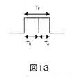
作動中、インターロゲーションシステム130が、モニタされるグレーティングGアレイの入った光ファイバ94に結合される場合、SOA82で透過(および増幅される)反射した光パルスは、後部反射CFBG132に出会い、反射光パルスの一部(〜1%)は、波長評価装置86に透過され、光パルスの残り(〜99%)は、SOA82に向かって再反射して戻る。電気駆動パルスの継続時間(Tp)、したがってSOA82がスイッチオンされる期間(Tpでもある)は、パルス伝搬時間TRよりも長いので、再反射した光パルスがSOA82に帰着するとき、SOA82は、依然スイッチオンのまま(すなわち、ゲートは依然開である)である。第一の再反射した光パルスの継続時間(またTp)は、また、パルス伝搬時間TRより長く、したがって、パルス透過時間より長い光パルスの一部である再反射した光パルスの一部は、SOA82を通って再び透過する際にさらなる増幅を経験する。これを図13に示す。
In operation, when the
したがって、伝搬時間TRは、インターロゲーションシステム130内で多重増幅および反射(循環)を受けることの可能な反射光パルスの部分を決定する。該SOA82は、反射光パルスへいくぶんかの広帯域バックグラウンドノイズを付加するけれども、再反射した光パルスは、モニタ中のグレーティングで反射した波長が支配する。したがって、SOA82にかけられた電気駆動パルスが、光パルスがモニタされる最も隣接したアレイ内グレーティング間を伝搬するのに要する時間の二倍より長ければいくぶんかの干渉が生じるが、生じた干渉は、光パルスが周期的増幅を受けない前述のインターロゲーションシステムにより経験されるものよりあまり重大でない。したがって、CFBG132とSOA82との間の距離が、より遅く作動するSOA82または駆動手段84内のより低速エレクトロニクスの使用を許容するために、微調整をなし得る。
Accordingly, the propagation time T R determines the possible portion of the reflected light pulses to undergo multiplex amplification and reflected by the
SOA82を去る再反射した、再増幅される光パルスは、モニタされるグレーティングによって最初に反射した波長、プラスSOA82からの低レベルの広帯域バックグラウンドノイズを含んでいる。光パルスは、前に記載したように、光ファイバ94に沿ってグレーティングGに向かって伝搬する。再び、パルスの一部は、アレイ内の各グレーティングから反射し、そして再び、一連の反射光パルス(時間および空間が離れている)がSOA82に帰着する。前のように、SOA82がスイッチオンしている間、一の反射光パルスのみが到着し、なぜなら、他のすべては、電気駆動パルスがSOA82にかけられる前または後のいずれかに到着するからである。選択された光パルスは、SOA82を通過する際に増幅され、そしてCFBG132に伝搬し、そこで循環が再び始まる。
The re-reflected, re-amplified light
反射光学素子(この実施例では、モニタされるファイバグレーティング)によって再反射した狭帯域波長は、SOA82の前後を周期的にトリップする際に多重増幅を経験する。SOA82によって生成した初期の低出力広帯域光パルスは、インターロゲーションシステム130を通して多重循環を受け、そして、光増幅の結果として、それは、SOA82の各通過において、強い狭帯域幅光パルスの迅速な形成を経験する。光パルスが得ることのできる最終光出力は、インターロゲーションシステム130内の損失の性質、ならびに使用したSOA82の飽和度および利得特性に依存する。
Narrowband wavelengths that are re-reflected by the reflective optical element (in this example, the monitored fiber grating) experience multiple amplification as they periodically trip around
前記したように、モニタのためのアレイ内の特定のグレーティングの選択は、SOA82にかける電気駆動パルスの周波数調整によって制御される。各パルスの継続時間は、CFBG132とSOA82との間のファイバ長の影響を考慮するように選択される。
As described above, the selection of a particular grating in the array for monitoring is controlled by frequency adjustment of the electrical drive pulse applied to
インターロゲーションシステム130が、モニタされるグレーティングGアレイの入った光ファイバ94に結合される場合、本発明の第21の実施態様に従う光センサシステム136が形成される。
When the
インターロゲーションシステム130内の光パルス循環によって経験される多重増幅のために、反射光学素子(この実施例では、モニタされるファイバグレーティング)がきわめて低反射率の場合でも、きわめて強い光パルスを生成することが可能である。低反射率グレーティングを使用することは、光パルスが各グレーティングで重大な出力損失を被らないで多くのグレーティングを通過できることを意味する。3-反射干渉は、また、低反射率グレーティングのために無視し得ることが示されている。したがって、センサアレイ内に低反射率グレーティングを使用すると、光センサシステム136にグレーティング間の干渉の生起を少なくしながらより多くのグレーティングを組み込むことが可能になる。
Due to the multiplex amplification experienced by the optical pulse circulation in the
インターロゲーションシステム130およびグレーティングセンサシステム136の周期的作動は、さまざまな利点を提供する。きわめて強い狭帯域幅光パルスが、共振波長の周辺に迅速に発生し、グレーティングがモニタされる。そのような強くかつ狭い波長の光信号は、さまざまなタイプの波長評価装置にとって測定が容易である。
The periodic operation of the
SOA82で生成した広帯域バックグラウンドノイズは、SOA82が強く狭い帯域幅を増幅するのに必要とされる場合に減少する。一旦、反射光パルスがインターロゲーションシステム130内で多数の循環を受け、(望む)主波長光信号が生成すると、出力の主波長(強く反射)への移行または尖鋭化が、広帯域バックグラウンドノイズを減少させる。これは、さらにSN比を増大させる。
The broadband background noise generated by
図14は、本発明の第21の実施態様に従うインターロゲーションシステム140を示す。この実施態様のインターロゲーションシステム140は、前述の実施態様のインターロゲーションシステムと実質的に同じであるが、以下が変更されている。同一の参照番号は、対応の特徴を維持する。
FIG. 14 shows an
この実施例では、インターロゲーションシステムは、さらに光ファイバ結合器142の形態の光ルーティングデバイスを含める。結合器142は、CFBG144とSOA82との間に位置し、該CFBG144は、結合器142のポートCおよびDを介してSOA82と結合する。波長評価装置86は、結合器142と結合する。
In this example, the interrogation system further includes an optical routing device in the form of a
この新規な光配列は、CFBG144で反射し、波長評価装置86へ透過する光信号であることを意味する。したがって、CFBG144は、現在、必要なら100%反射率まで作られる。上記したように、CFBG144でカバーされるスペクトル帯域は、モニタされるグレーティングの操作域のみをカバーするように選択することができる。これは、波長評価装置86までルーティングされる光信号がCFBG144のスペクトル帯域内に位置する波長のみを含むことを意味する。したがって、波長評価装置で見られるSOA-生成ノイズは、CFBG144(そして、それゆえグレーティングGの操作帯域)のスペクトル帯域内にあるものになる。このスペクトル帯域の外にある波長の全光信号は、CFBG144によって反射されず、したがって、波長評価装置86に到達しない。これは、波長評価装置86におけるSN比を増大する方へ導く。
This new optical arrangement means that the optical signal is reflected by the
さらに、CFBG144のスペクトルプロファイルは、モニタされるグレーティングの作動スペクトル帯域のみをカバーするので、CFBG144の存在は、SOA82で増幅されるアウト-オブ-バンド信号を減少させ、これによりその効率を改善する。
Furthermore, since the spectral profile of
インターロゲーションシステム140に結合器142を含めるために、SOA82とCFBG144との間の最小離隔距離を増大させる必要がある。したがって、SOA82への電気駆動パルスの継続時間もまた、増大させる必要がある。結合器142の存在は、インターロゲーションシステム140内の光損失の増大を生じる。損失量(ポートAを通る)は、選択した結合器の結合比(coupling ratio)(50:50,60:40など)で決定される。より低い結合比を選ぶと、より低い損失になるが、波長評価装置86へより低い光信号を提供することになる。しかし、より高反射率のCFBG144を用いて生成されるインターロゲーションシステム140内のゲインの増大とSOA82が経験するより低いアウト-オブ-バンドノイズは、結合器142が被る損失のいくぶんかをオフセットするのに使用することができる。
In order to include the
モニタ装置140をモニタされるグレーティングGのアレイの入った光ファイバ94に結合すると、それらは一緒になって、本発明の第22の実施態様に従う光センサシステム146を形成する。
When the
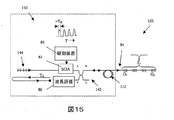
本発明の第23の実施態様に従うインターロゲーションシステムを図15に示す。この実施態様は、前述の実施態様に同じであるが、以下が変更されている。同一の参照番号は、対応の特徴を維持する。 An interrogation system according to a twenty-third embodiment of the present invention is shown in FIG. This embodiment is the same as the previous embodiment, with the following changes. The same reference number maintains the corresponding feature.
この実施例では、結合器142はSOA82の他側で、SOA82と追加のファイバ112との間にポートAおよびBを介して位置する。結果として、パルスが最初にSOA82を通過しないで、波長評価装置86は、モニタされるグレーティングから反射光パルスを直接受信する。
In this embodiment,
これは、波長評価装置が受信した反射光パルスは、SOA82からのアウト-オブ-バンドノイズを全く含まないことを意味する。したがって、波長評価装置86へ透過する光パルスのSN比が改善される。
This means that the reflected light pulse received by the wavelength evaluation device does not include any out-of-band noise from the
インターロゲーション装置150をモニタされるグレーティングGアレイの入った光ファイバ94に結合すると、それらは一緒になって、本発明の第24の実施態様に従う光センサシステム152を形成する。
When the
図16に、本発明の第24の実施態様に従うインターロゲーションシステム160を示し、これは、図14に示すインターロゲーションシステム140と実質的に同じであるが、以下が変更されている。同一の参照番号は、対応の特徴を維持する。
FIG. 16 shows an
インターロゲーションシステム140(図14)に必要とされる電気駆動パルス継続時間のすべての増大が、結合器142の存在のために、循環反射光信号の増幅に寄与するわけではない。電気駆動パルスの主部によって、モニタされるグレーティングから到達する反射光信号が、開のSOA82を通過する際に増幅される。電気駆動パルスの従部によって、CFBG144帰還した再反射光パルスが、さらにSOA82を通ってグレーティングGに向かって戻る際に増幅される。電気駆動パルスの中央部は、有用な目的のために働くわけでなく、なぜなら電気駆動パルスのこの部分の間は、反射した光パルスがSOA82とCFBG144との間を伝搬しているからである。したがって、この時にSOA82に適用されたいかなる電気駆動信号も、望まないノイズを生成する。その結果は、伸張された電気駆動パルスがSOA82の電気効率を減じるのみで、そしてインターロゲーションシステム140のSN比を劣化させる。
Not all increases in electrical drive pulse duration required for interrogation system 140 (FIG. 14) contribute to the amplification of the circular reflected light signal due to the presence of
これらの非効率は、図16の挿入図(a)に示すように、電気駆動パルス対のストリームを使用することによって克服することが可能である。したがって、結合器を介するSOA82とCFBG144との間の全パス長は、あまり重要でなくなる(この実施例では、典型的には2〜3mになろう)。
These inefficiencies can be overcome by using a stream of electrically driven pulse pairs, as shown in the inset (a) of FIG. Thus, the total path length between
各電気駆動パルスの継続時間は、上記したように、光パルスがモニタされるグレーティングアレイの最も近くに隣接するグレーティングG間を伝搬するのにかかる時間の二倍よりも短くなるように設定される。パルス対の全サイクルについての全反復期間(TT)は、上記したように、反射光パルスがモニタ中のグレーティングからCFBG144へ透過するのに要する時間の二倍に等しい。各対内の二パルス間の期間(TR)は、反射光パルスがSOA82からCFBG144へ伝搬し、そしてSOA82へ戻るのに要する時間に等しくなるように設定される。
The duration of each electrical drive pulse is set to be shorter than twice the time it takes for the light pulse to propagate between adjacent gratings G closest to the grating array being monitored, as described above. . The total repetition period (T T ) for the entire cycle of the pulse pair is equal to twice the time required for the reflected light pulse to pass from the grating being monitored to the
したがって、中央領域が有用な目的のために働かない単一のブロードな電気駆動パルスを有する場合の代わりに、中央部は効果的に除去され、残るは二つの短電気駆動パルスである。各対中の第一の電気駆動パルスは、反射光パルスがモニタされるグレーティングから到着する際にSOA82をスイッチオンするように働き、これにより反射光パルスを透過および増幅する。第二の電気駆動パルスは、再反射した光パルスがCFBG144から戻って来る際にSOA82をスイッチオンするように作用し、これにより、モニタされるグレーティングへ戻る光パルスを透過(および増幅)する。
Thus, instead of having a single broad electric drive pulse where the central region does not work for useful purposes, the central portion is effectively removed and the remaining two short electric drive pulses. The first electrical drive pulse in each pair serves to switch on the
インターロゲーションシステム160をモニタされるグレーティングGアレイの入った光ファイバ94を結合することにより、本発明の第26の実施態様光センサシステム162を形成する。
The
本発明の第27の実施態様に従う光インターロゲーションシステム170を、図17に示す。このインターロゲーションシステム170は、実質的に図16に示すインターロゲーションシステム160と同一であるが、以下の変更がある。同一の参照番号対応の特徴を維持する。
An
前述の実施態様に示す一の反射光学素子が、モニタされる反射光学素子のアレイ内特定位置にあるとき、一グループの反射光学素子(この実施例では、グレーティング172)を位置づけることが実際に可能である。グループ内の各グレーティング172は、異なる波長窓内で作動する。この実施態様のインターロゲーションシステム170は、そのようなグレーティンググループのアレイをモニタすることを予定している。グループ172内の各グレーティングの共振波長は、異なる波長窓内にあるので、したがって、各グレーティングは、異なる光チャンネル内で作動する。例えば、各グループ172は、C-バンドが1530nm、1535nm、1540nm、1545nm、1550nm、1555nmおよび1560nmで、各光チャンネルがそれぞれ5nm幅を作る7個のFBG、好適な共振波長を含み得る。この実施例では、グレーティングは、それぞれ、2.5mmの長さ、0.2nmの帯域幅および4%の透過損失を有する。各グループ172内のグレーティングは、電気駆動パルスの半分の間、光信号でカバーされる伝搬距離より短い距離だけ離れている必要があり、この実施例では、10cmだけ離れている。
It is actually possible to position a group of reflective optical elements (in this example, a grating 172) when one reflective optical element shown in the previous embodiment is at a particular position in the array of monitored reflective optical elements. It is. Each grating 172 in the group operates in a different wavelength window. The
各グループ172は、同一セットの共振波長を有する同数のグレーティングを含む。隣接するグループ172内の等価なグレーティングは、1mだけ離れており、例えば一グループ内の1540nmグレーティングは、隣接するグループ内の1540nmグレーティングから1m離れている。
Each
そのようなグループ172内に配置されるモニタされるグレーティングを有することの結果は、作動の間、SOA82によって生成される各広帯域光パルスにとって、多重反射光パルス(グループ172内の各グレーティングからの反射)は、ほぼ同時にSOA82に戻って来ることである。したがって、SOA82へかけられる各対内の第一電気駆動パルスは、SOA82にグレーティング172の特定のグループに対応した全反射光パルスを透過させる。
The result of having a monitored grating placed in such a
SOA82によって透過した多重反射光パルスを分離するために、前述の実施態様の単一のCFBG144光反射器を、FBG174、176のアレイ(図17には、明確性のために、最初の二個のみ示す)の形態の一連の光反射器に代える。各FBG174、176は、異なるスペクトル帯域内で波長を反射し、波長窓に対応した各スペクトル帯域は、モニタされるグレーティングが作動する一の光チャンネルでカバーされる。この実施例では、各FBG反射器174、176の帯域幅、したがって光チャンネルのものは5nmである。
In order to separate the multiple reflected light pulses transmitted by SOA82, the single CFBG144 light reflector of the previous embodiment is replaced with an array of
各FBG反射器174、176は、SOA82から異なる距離に位置する。この実施例では、隣接するFBG反射器174、176は、1mだけ離れている。結果として、SOA82から個々のFBG反射器174、176の飛行時間および戻ってくる時間は、グループ172内のどのグレーティングから光パルスが反射するかに依存する。
Each
したがって、前のように、対内の電気駆動パルス間の期間TRおよびパルス対間の期間TTの微調整により、特定のグループ172内の特定グレーティングをモニタするために選択することができる。
Thus, as before, a particular grating in a
インターロゲーションシステム170を、モニタされるグレーティングのグループ172の入ったファイバ94と結合することにより、本発明の第28の実施態様に従う光センサシステム178を形成する。
The
操作中、第一対内の第二電気駆動パルスは、SOA82にモニタされるグレーティングに向かって伝搬する光パルスを生成させる。光パルスの一部は各グレーティングによって反射され、それぞれが個々のグレーティングに対応したピーク波長を有する一連の反射光パルスを生じさせる。グループ172内の特定のグレーティングの反射光信号は、後続の電気駆動パルス対内の第一電気駆動パルスをSOA82にかけるのに対応してほぼ同時にSOA82に戻って来る。したがって、この反射光信号グループは、SOA82によって透過および増幅され、そこから、FBG反射器174、176のアレイの前に続く。
During operation, the second electrical drive pulse in the first pair generates an optical pulse that propagates toward the grating monitored by the
各FBG反射器174、176は異なる光チャンネルをカバーするので、各反射光信号は、異なるFBG反射器174、176から再反射される。したがって、再反射光信号は、時間および空間が離れているSOA82へ向かって伝搬して戻る。唯一の再反射した光パルスが、SOA82が電気駆動パルス第二対内の第二の電気駆動パルスによってスイッチオンしている間にSOA82に到着する。再反射光信号の他の全部は、それがオフの間に到着するので、センサシステム178内でのさらなる循環が阻止される。
Since each
選択された光パルスは、SOA82によって透過および増幅され、もう一度、グレーティングに向かって伝搬し、そこで再び、モニタのために選択されたグレーティングによって反射され、循環を繰り返す。
The selected light pulse is transmitted and amplified by the
対内の両電気駆動パルスは、光パルスを生成させるけれども、システムのサイクル性のために、グレーティングの一のグループ172のみが循環増幅を受け、そしてピークに達する。したがって、グレーティングの他のグループからの潜在的な干渉を無視することができる。
Both electrical drive pulses in the pair generate optical pulses, but due to the cyclic nature of the system, only one
インターロゲーションシステム170およびセンサシステム178は、以下の利点を提供する。一のみの反射光信号が、波長評価装置86に示される。これは、採用し得る波長評価技術の可能な幅を拡げる。特に、波長窓の全域にわたって操作可能な、特色のない繰り返し関数波長評価装置(colourless, repeated function, wavelength evaluation apparatus)の使用を受け入れる。例えば、波長依存性透過関数を有する上記の光フィルタを、ファブリー−ペローフィルタやエタロンスロープフィルタで代替でき、これらは光損失を減じるために光ファイバ内に組み込むことができる。
さらに、一のみの反射光パルスが、あらゆる時にセンサシステムでサポートされるので、SOA82の全光増幅出力を単一光パルスへ集中することができる。SOA82の光出力は、多数の反射光信号の間で分配される必要がなく、したがって、光チャンネル間で不安定性の可能性や出力コンフリクトが存在しない。
Furthermore, since only one reflected light pulse is supported by the sensor system at any time, the all-optical amplified output of
図18は、本発明の第29の実施態様に従う光インターロゲーションシステム180を示す。インターロゲーションシステム180は、実質的に図 17のインターロゲーションシステム170と同じであるが、以下が変更されている。同一の参照番号は、対応の特徴を維持する。
FIG. 18 shows an
この実施態様では、光パルスはパルス光源182によって生成され、SOA82は、光増幅およびゲート制御デバイスとして機能することが制限される。SOA82ゲートに選択的に光パルスをパルス光源182から光ファイバ94へ結合させるための複雑な時間調整の必要を回避するために、パルス光源が、SOA82と追加長のファイバ112との間の光ファイバ94にファイバ結合器184を介して結合される。
In this embodiment, the light pulses are generated by a pulsed
インターロゲーションシステム180を、モニタされるグレーティングのグループ172のアレイの入った光ファイバ94と結合することにより、本発明の第30の実施態様に従う光センサシステム186が形成される。
Combining the
本発明の第31の実施態様に従う光導波路インターロゲーションシステム190を図19に示す。このインターロゲーションシステム190は、実質的に図17のインターロゲーションシステム170と同じであるが、以下が変更されている。同一の参照番号は、対応の特徴を維持する。
An optical
この実施例では、結合器142および波長評価装置86は、SOA82のグレーティングアレイ側へ移動している。図17に関連して上記したように、FBG反射器174、176から反射した光パルスの一のみが、SOA82がスイッチオンしている間にSOA82に戻ってくる。再反射光信号の他の全ては、SOA82がスイッチオフのときに到着するので、さらなる透過がブロックされる。したがって、波長評価装置86をSOA82のこちら側へ位置させることは、所望の反射光信号の選択性を増大し、そして波長評価装置86に示される光信号から他波長を除去するという利点を有する。
In this embodiment, the
インターロゲーションシステム190を、モニタされるグレーティングアレイの入った光ファイバ94と結合することにより、本発明の第32の実施態様に従う光センサシステム192が形成される。
By combining the
本発明の第33の実施態様に従う光導波路インターロゲーションシステム200を図20示す。センサシステム200は、図17に示すような光インターロゲーションシステム170を使用するが、別法として、図18に示すような光インターロゲーションシステム180や図19に示すような光インターロゲーションシステム190を使用してもよい。
An optical
この実施例では、センサシステム200はまた、センサグレーティングアレイ206、208をそれぞれ含む二本のファイバ202、204を備える。ファイバ202、204は、インターロゲーションシステム170にWDM多重化復調器(MUX-DEMUX)210を介して結合する。操作中、MUX-DEMUX210は、一側の単一ポート212に示される多くの光チャンネルの入った複合光信号を複数の光信号(各光チャンネルにつき一)に逆多重化する。逆多重化された光信号のそれぞれは、MUX-DEMUXの反対側の異なる一出力ポートを介して出力される。各出力ポートは、異なる光チャンネルをサポートする。MUX-DEMUX210は、また、逆に複数の光信号を単一の複合光信号へ多重化通信するように作動する。この実施例では、二の光チャンネルのみが使用されるので、二の出力ポート214、216のみが使用される。
In this embodiment, the
アレイ内の各グレーティング206、208は、同一の共振波長を有し、すなわち、アレイ内の全グレーティング206、208は、同一光チャンネル内で作動する。特定のファイバ202、204内のグレーティング206、208が作動する光チャンネルは、ファイバ202、204が結合するMUX-DEMUX210の出力ポート214、216によってサポートされる光チャンネルに対応する。
Each grating 206, 208 in the array has the same resonant wavelength, ie, all the
上記したように、インターロゲーションシステム170は、空間的にも波長チャンネル別にもグレーティングを区別するように動作可能である。したがって、二本のファイバ202、204内のいずれかのグレーティング206、208を個々にモニタすることが可能である。
As described above, the
モニタされるグレーティング206、208のアレイの入った二本のファイバ202、204のみをMUX-DEMUX210の出力ポートに結合するように見せているが、より多数のファイバ、およびしたがってグレーティングアレイを備えることが理解される。サポート可能な異なるグレーティングアレイの数は、インターロゲータ170およびMUX-DEMUX210の機器構成によりモニタすることの可能な波長チャンネルの数に制限される。
Although only two
グレーティング206、208の多重アレイを単一のインターロゲータ170に結合するためにWDM MUX-DEMUX210を使用すると、結合器(図5に示すような)を使用する場合と比べて、センサシステム200内に存在する光損失を低減する。単一センサシステム200内に大多数グレーティングアレイを持ち得る能力は、測定を比較的広い空間に位置するセンサ用途において利点である。
Using a WDM MUX-
本発明の第34の実施態様に従う光導波路インターロゲーションシステム220を図21示す。このインターロゲーションシステム220は、実質的に図7のインターロゲーションシステム80と同じであるが、以下が変更されている。同一の参照番号は、対応の特徴を維持する。
An optical
この実施態様では、光学検知手段は、光検出器222の形態をとる。
In this embodiment, the optical sensing means takes the form of a
光インターロゲーションシステム220は、光パルス発信器(OTDR)のように動作可能である。図21に示すように、OTDR220は、例えば、光ファイバ228内の破断部224の形態の反射光学素子やパッチコード連結部226、あるいは光ファイバ228の末端230をモニタするのに用いることができる。
The
図22は、本発明の第35の実施態様に従う光インターロゲーションシステム240を示す。光インターロゲーションシステム240は、実質に前述の実施態様のシステム220と同様であるが、以下が変更されている。同一の参照番号は、対応の特徴を維持する。
FIG. 22 shows an
この実施態様では、光インターロゲーションシステム240は、さらにSOA82および光検出器222間の帰還光信号の光パス内に設けられるファイバブラッググレーティング(FBG)242の形態の光信号ルーティング手段を含む。FBG242は、一部の帰還光信号が光検出器222へ透過される一方、大部分の帰還光信号がFBG242で反射するように100%より低い反射率を有する。図12と関連して上述したように、帰還光信号の反射部分は、SOA82を通って伝搬して戻り、調査中の反射光学素子へ向かって伝搬して戻る。光インターロゲーションシステム240は、OTDRとして動作可能である。
In this embodiment, the
図23に、本発明の第36の実施態様に従う光インターロゲーションシステム250を示す。光インターロゲーションシステム250は、実質的に前述の実施態様のシステム240と同様であるが、以下が変更されている。同一の参照番号は、対応の特徴を維持する。
FIG. 23 shows an
この実施態様では、光検出器222は、FBG242とSOA82との間でFBG242の反対側に位置する。光検出器222は、低パーセンテージ光結合器252を用いて光インターロゲーションシステム250へ結合される。この配置は、FBG242で反射した帰還光信号の一部のみが光検出器222へルーティングされるという利点を有する。FBG242の反射帯域幅の外側でSOA82によって生成されるいかなる増幅自然放出(ASE)ノイズも透過され、そしてこれにより除去される。
In this embodiment, the
図24に、本発明の第37の実施態様に従う光インターロゲーションシステム260を示す。光インターロゲーションシステム260は、実質的に前述の実施態様のシステム250と同様であるが、以下が変更されている。同一の参照番号は、対応の特徴を維持する。
FIG. 24 shows an
この実施態様では、光検出器222は、SOA82の他側に位置し、光結合器252を介してシステム260へ結合される。この配置は、帰還光信号の反射部分は、さらに光検出器222を通過する前にSOA82によって増幅されているという利点を提供する。
In this embodiment, the
図25に、本発明の第38の実施態様に従う光インターロゲーションシステム270を示す。光インターロゲーションシステム270は、実質的に図23に示すシステム250と同様であるが、以下が変更されている。同一の参照番号は、対応の特徴を維持する。
FIG. 25 shows an
この実施態様では、第二のFBG272の形態の第二の光信号ルーティング手段が、第一FBG242に隣接して設けられる。二のFBG242、272は、異なる共振波長を有する。図17に示す光インターロゲーションシステム170と同様に、駆動手段84は、駆動パルス対を生成する。各対内の第一の駆動パルスは、モニタされる反射光学素子の入った光ファイバ228へ光信号パルスを生成および放出させる。第一駆動パルスは、また、帰還光信号をゲート制御して、どれをFBGS242、272へ透過させるか選択する。透過した帰還光信号は、その波長に応じて、FBG242、272の一によって反射される。第一駆動パルスと第二駆動パルスとの分離は、FBG242、272のどちらを使用するかを選択し、これにより波長帯域幅の動作を選択する。
In this embodiment, a second optical signal routing means in the form of a
この配置は、波長依存性反射特性を有する反射光学素子を備えた光システムにとって利点である。これにより、例えば、ファイバ破断部(これは全波長に影響する)を特定の反射光学素子の波長ドリフト(これは全波長に影響しない)と区別することが可能となる。 This arrangement is advantageous for optical systems with reflective optical elements that have wavelength dependent reflective properties. This makes it possible to distinguish, for example, a fiber break (which affects all wavelengths) from the wavelength drift of a particular reflective optical element (which does not affect all wavelengths).
記載された実施態様は、以下のさまざまな利点を提供する。SOAを同時に広帯域源ならびに複合化された光ゲートおよび増幅手段として使用することは、インターロゲーションシステムをアクティブ光デバイス(active optical component)で、あるいはモニタされる反射光学素子アレイの別個について一の光学要素で構築できることを意味する。これは、多くの公知の既存システムと比べて、インターロゲーションシステムの全体サイズおよびコストを低減し、そして効率および信頼性の改善を提供する。時分割多重型インターロゲーションシステムを使用する記載された光センサシステムでは、全グレーティングは同一であり得、これは製造および設置手順の両方を簡素化する。グレーティングは、別法として、異なるタイプの反射光学素子であるが、各要素は同一であるものへ代替することも可能である。 The described embodiment provides the following various advantages. The simultaneous use of SOA as a broadband source and combined optical gate and amplification means makes it possible to use an interrogation system as an active optical component or separate optical array of reflective optics to be monitored. It means that it can be constructed with elements. This reduces the overall size and cost of the interrogation system and provides improved efficiency and reliability compared to many known existing systems. In the described optical sensor system using a time division multiplexed interrogation system, the entire grating can be the same, which simplifies both the manufacturing and installation procedures. The grating is alternatively a different type of reflective optical element, but each element can be replaced by the same one.
SOAとモニタされる反射光学素子アレイとの間に追加長の光ファイバを設けることにより、SOAが電気駆動パルスの連続ストリームで駆動されることが可能になり、ここで、SOAは、光パルス源の一部を形成し、反射光学素子アレイが光パルスの連続のストリームを使用してモニタされることを可能とする。これは、基礎的で公知なTDM型インターロゲーションシステムと比べて、効率を改善したインターロゲーションシステムを生む。 By providing an additional length of optical fiber between the SOA and the reflective optics array to be monitored, the SOA can be driven with a continuous stream of electrical drive pulses, where the SOA is an optical pulse source. And allowing the reflective optics array to be monitored using a continuous stream of light pulses. This yields an interrogation system with improved efficiency compared to the basic and well-known TDM type interrogation system.
一以上のFBGバック反射器をインターロゲーションシステムへ組み込むこと、および光パルスにセンサシステム内を循環させることは、さまざまな利点を提供する。低反射率反射光学素子、例えば低反射率FBGを、光センサシステム内で使用可能である。低反射率FBGは、作製が安価であり、3−反射干渉をあまり受けず、そして、出力レベルが許容レベル以下に落ちる前に高反射率グレーティングよりも大多数のグレーティングをアレイ内で使用可能とする。 Incorporating one or more FBG back reflectors into an interrogation system and circulating light pulses through the sensor system provides various advantages. A low reflectivity optical element, such as a low reflectivity FBG, can be used in an optical sensor system. Low reflectivity FBGs are inexpensive to make, are less susceptible to 3-reflection interference, and can use a greater number of gratings in the array than high reflectivity gratings before the output level falls below acceptable levels To do.
光パルスの循環は、また、高いSN比(SNR)を達成できることを意味し、なぜならSOAのパワーが支配的サイクル波長に集中され、SOAによって生成される広帯域ASEノイズを低減させるからである。 Optical pulse cycling also means that a high signal-to-noise ratio (SNR) can be achieved because the power of the SOA is concentrated at the dominant cycle wavelength, reducing the broadband ASE noise generated by the SOA.
循環パルスは、また、緩慢な電気的および光応答時間(与えられたSNRで)について非循環パルスで期待されるよりもより寛容である。これは、光センサシステム内の反射光学素子を、非循環パルスを使用するときに可能なものより、それらの間により小さい分離を持たせればよいことを意味する。 Circulating pulses are also more forgiving than expected with non-circulating pulses for slow electrical and optical response times (with a given SNR). This means that the reflective optical elements in the optical sensor system should have a smaller separation between them than is possible when using non-circulating pulses.
電気駆動パルス対を使用することにより、インターロゲーションシステムおよびセンサシステムのSNRが、さらに一層増大し、そして電気効率が改善される。さらに、電気駆動パルスタイミングの調整は、アクティブ選択を可能とし、その反射光信号および反射光学素子は、再反射信号にSOAで再透過させるためにどのFBGバック反射器がSOAからの正しい距離であるかを選択することによりモニタされる。 By using electrically driven pulse pairs, the SNR of the interrogation system and sensor system is further increased and the electrical efficiency is improved. In addition, adjustment of the electrical drive pulse timing allows active selection, and its reflected light signal and reflective optics are the correct distance from the SOA which FBG back reflector to re-transmit the re-reflected signal with the SOA Is monitored by selecting.
多重バック反射器の使用により、インターロゲーションシステムはWDMおよびTDMの両方を使用することが可能となる。これは、さらにモニタされる反射光学素子間の間隔を減じ、そしてそれにより光センサシステム内の全反射光学素子数を増大し、あるいはセンサシステムに別個の反射光学素子アレイを組み込ませるのに使用する。 The use of multiple back reflectors allows the interrogation system to use both WDM and TDM. This is further used to reduce the spacing between the reflective optical elements to be monitored and thereby increase the number of total reflective optical elements in the optical sensor system, or allow the sensor system to incorporate a separate reflective optical element array. .
インターロゲーションシステムがWDMおよびTDMの両方を使用するとき、インターロゲーションシステムは、単一光信号を一時に出力可能であり、これは波長評価装置にてより広範囲の波長インターロゲーション技術を可能にする。 When an interrogation system uses both WDM and TDM, the interrogation system can output a single optical signal at a time, which allows a wider range of wavelength interrogation technologies in wavelength evaluation equipment To.
記載された実施態様に対してさまざまな変更が本発明の範囲から逸脱せずになし得る。特に、当業者は、記載されたファイバグレーティング、ファイバ破断部およびパッチコードコネクタに代えて、異なるタイプの反射光学素子を使用可能であることに気づく。反射光学素子は、以下のいずれでもよい:バルクオプティックファブリー−ペローエタロンであり得るファブリー−ペローエタロンデバイス;光ファイバファブリー−ペローエタロン;光導波路グレーティング型ファブリー−ペローエタロン;終端が鏡面であり得る光ファイバの端部;光ファイバパッチコードの端部;光ファイバセクション内の破断部;結晶をベースとする反射光学素子;またはミラー部材。 Various modifications to the described embodiments can be made without departing from the scope of the invention. In particular, those skilled in the art will recognize that different types of reflective optical elements can be used in place of the described fiber gratings, fiber breaks and patch cord connectors. The reflective optical element may be any of the following: a Fabry-Perot etalon device that may be a bulk optic Fabry-Perot etalon; an optical fiber Fabry-Perot etalon; an optical waveguide grating type Fabry-Perot etalon; an optical fiber whose termination may be a mirror surface An end of an optical fiber patch cord; a break in an optical fiber section; a crystal-based reflective optical element; or a mirror member.
記載された三つの異なる広帯域光パルス源、すなわち、CW広帯域光源プラスSOA、SOA自身およびパルス光源は、交換可能に使用できる。記載されたSLDは、他のいずれかの適当なCW広帯域光源で置換可能である。当業者が理解するように、光源の選択は、少なくとも一部はモニタされる反射光学素子の波長域に依存し、なぜなら、光源は、それらの波長を含む光信号を生成するように動作可能である必要がある。 The three different broadband optical pulse sources described, namely CW broadband light source plus SOA, SOA itself, and pulsed light source can be used interchangeably. The described SLD can be replaced with any other suitable CW broadband light source. As one skilled in the art will appreciate, the choice of light source will depend at least in part on the wavelength range of the reflective optical element being monitored, because the light source is operable to generate an optical signal that includes those wavelengths. There must be.
モニタされる反射光学素子がグレーティングとして記載されている場合、異なる数のグレーティングを使用可能であり、そしてグレーティングは、記載されたものと異なる共振波長を有してもよい。アレイ内グレーティングは、また、記載されたものより異なる距離だけ離れていてもよい。 If the reflective optical element to be monitored is described as a grating, a different number of gratings can be used, and the grating may have a different resonant wavelength than that described. The in-array gratings may also be separated by different distances than those described.
各インターロゲーションシステムは、一以上の反射光学素子アレイ、例えば図5に示すグレーティングを使用してよく、したがって、各センサシステムは、一以上の反射光学素子アレイを含み得る。 Each interrogation system may use one or more reflective optical element arrays, such as the grating shown in FIG. 5, and thus each sensor system may include one or more reflective optical element arrays.
ファイバブラッググレーティングが記載されている場合、別法として、平面ブラッググレーティングを使用可能であり、そしてブラッググレーティングは、他のタイプの光導波路グレーティングによって代替可能である。 Where fiber Bragg gratings are described, alternatively, planar Bragg gratings can be used, and the Bragg gratings can be replaced by other types of optical waveguide gratings.
当業者が理解するように、平面光導波路グレーティングを使用するならば、記載された光ファイバは、平面光導波路で代替できる。これにより、全インターロゲーションシステムを、ハイブリッド平面光波回路として組み立てることが可能になり、前記回路は、SOA、駆動エレクトロニクス、光素子、例えば光フィルタおよびバック反射器ならびに光結合器またはサーキュレータを組み込む。記載されたSOAは、パルス操作可能な他の光増幅およびゲート手段で代替可能である。別法として、特に利得クランプSOAを使用し得る。 As will be appreciated by those skilled in the art, if a planar optical waveguide grating is used, the described optical fiber can be replaced by a planar optical waveguide. This allows the entire interrogation system to be assembled as a hybrid planar lightwave circuit, which incorporates SOA, drive electronics, optical elements such as optical filters and back reflectors and optical couplers or circulators. The described SOA can be replaced by other optical amplification and gating means that can be pulsed. Alternatively, in particular a gain clamp SOA can be used.
記載された波長評価装置、すなわち、波長計および光フィルタプラス光検出器は、交換可能に使用し得る。伝達関数に依存可能な波長を有する光フィルタは、バルクオプティックデバイスであり得、または光導波路グレーティングデバイス、例えば傾斜ブラッググレーティング(われわれの英国特許出願GB0013411.4およびPCT/GB01/02422に記載されたような)であり得る。 The described wavelength evaluation apparatus, ie a wavelength meter and an optical filter plus photodetector, can be used interchangeably. An optical filter having a wavelength that can depend on the transfer function can be a bulk optic device or an optical waveguide grating device, such as a tilted Bragg grating (as described in our UK patent applications GB0013411.4 and PCT / GB01 / 02422). N).
以下の光パルス源内または後続するように設けられる光フィルタは、記載されたものと異なるスペクトル透過プロファイルを有してもよい。同様に、波長評価装置の前に設けられる光フィルタは、記載されたものと異なるスペクトル透過プロファイルを有してもよい。CFBGバック反射器は、記載されたものと異なるスペクトルプロファイルを有してよく、および異なる光反射器、特に異なる光ファイバグレーティングあるいは異なる平面光導波路グレーティングで代替してもよい。一以上のバック反射器を使用する場合、記載されたものと異なる数のバック反射器を使用してよく、そして、隣接するバック反射器間の間隔が異なっていてもよい。 The optical filters provided in or following the optical pulse source below may have a spectral transmission profile different from that described. Similarly, the optical filter provided in front of the wavelength evaluation device may have a spectral transmission profile different from that described. The CFBG back reflector may have a different spectral profile than that described, and may be replaced with a different light reflector, particularly a different fiber optic grating or a different planar optical waveguide grating. If more than one back reflector is used, a different number of back reflectors than those described may be used, and the spacing between adjacent back reflectors may be different.
Claims (11)
波長評価装置(18,86)と、
該導波路に光結合する双方向光増幅およびゲート手段(14,82)とを含み、
該波長評価装置は、該光増幅およびゲート手段に光結合し、該光増幅およびゲート手段によって透過された帰還光パルスの波長を検知するように動作可能であり、
該双方向光増幅およびゲート手段(14,82)は、単一の光学機器であり、モニタ中のグレーティングから帰還される光パルスを選択的に透過し、かつ同時にそこを透過された光信号を光増幅するように動作可能であることを特徴とする、光導波路グレーティングインターロゲーションシステム(10,40,80,130,14,170)。A light source (12 and 14, 42, 82) operable to generate a light pulse, coupled to an optical waveguide (16, 94) comprising one or more monitored gratings (24, G 1-n ) The light source,
Wavelength evaluation device (18, 86);
Bi-directional optical amplification and gating means (14, 82) optically coupled to the waveguide;
The wavelength evaluation device is operable to optically couple to the optical amplification and gate means and detect a wavelength of a feedback light pulse transmitted by the optical amplification and gate means;
The bidirectional optical amplification and gating means (14, 82) is a single optical instrument that selectively transmits an optical pulse fed back from the grating being monitored and simultaneously transmits the optical signal transmitted therethrough. Optical waveguide grating interrogation system (10, 40, 80, 130, 14, 170), characterized in that it is operable to optically amplify.
該光増幅およびゲート手段(14)がスイッチオン・オフする際に連続波光信号を光パルス中へゲート制御する、請求項1〜3のいずれか一項に記載の光導波路グレーティングインターロゲーションシステム。The light source includes a continuous wave light source coupled to the bidirectional optical amplification and gating means and operable to generate a continuous wave optical signal, such as a superluminescent photodiode (12);
4. An optical waveguide grating interrogation system according to any one of claims 1 to 3, wherein the optical amplification and gating means (14) gates a continuous wave optical signal into an optical pulse when it is switched on and off.
Applications Claiming Priority (5)
| Application Number | Priority Date | Filing Date | Title |
|---|---|---|---|
| EP02258640.8 | 2002-12-16 | ||
| EP02258640A EP1432149B1 (en) | 2002-12-16 | 2002-12-16 | Optical waveguide grating interrogation system and sensor system |
| US10/665,840 US7046349B2 (en) | 2002-12-16 | 2003-09-19 | Optical interrogation system and sensor system |
| US10/665,840 | 2003-09-19 | ||
| PCT/GB2003/005497 WO2004056017A1 (en) | 2002-12-16 | 2003-12-15 | Optical interrogation system and sensor system |
Publications (2)
| Publication Number | Publication Date |
|---|---|
| JP2006524793A JP2006524793A (en) | 2006-11-02 |
| JP4817423B2 true JP4817423B2 (en) | 2011-11-16 |
Family
ID=32338174
Family Applications (1)
| Application Number | Title | Priority Date | Filing Date |
|---|---|---|---|
| JP2005502463A Expired - Fee Related JP4817423B2 (en) | 2002-12-16 | 2003-12-15 | Optical interrogation system and sensor system |
Country Status (7)
| Country | Link |
|---|---|
| US (1) | US7046349B2 (en) |
| EP (1) | EP1432149B1 (en) |
| JP (1) | JP4817423B2 (en) |
| CN (1) | CN1726664B (en) |
| AT (1) | ATE369670T1 (en) |
| DE (1) | DE60221681T2 (en) |
| ES (1) | ES2294086T3 (en) |
Families Citing this family (77)
| Publication number | Priority date | Publication date | Assignee | Title |
|---|---|---|---|---|
| GB0217273D0 (en) * | 2002-07-25 | 2002-09-04 | Diomed Ltd | Laser system |
| GB0322859D0 (en) * | 2003-09-30 | 2003-10-29 | British Telecomm | Communication |
| US7667849B2 (en) * | 2003-09-30 | 2010-02-23 | British Telecommunications Public Limited Company | Optical sensor with interferometer for sensing external physical disturbance of optical communications link |
| GB0407386D0 (en) * | 2004-03-31 | 2004-05-05 | British Telecomm | Monitoring a communications link |
| US7492463B2 (en) | 2004-04-15 | 2009-02-17 | Davidson Instruments Inc. | Method and apparatus for continuous readout of Fabry-Perot fiber optic sensor |
| WO2005116706A2 (en) * | 2004-05-15 | 2005-12-08 | The Board Of Trustees Of The Leland Stanford Junior University | Method of characterizing fiber bragg gratings using iterative processing |
| KR100609697B1 (en) * | 2004-06-02 | 2006-08-08 | 한국전자통신연구원 | Optical time-domain reflectometer system with gain-clamped optical amplifiers |
| GB0421747D0 (en) * | 2004-09-30 | 2004-11-03 | British Telecomm | Distributed backscattering |
| US7848645B2 (en) * | 2004-09-30 | 2010-12-07 | British Telecommunications Public Limited Company | Identifying or locating waveguides |
| US7292754B2 (en) * | 2004-12-15 | 2007-11-06 | Northrop Grumman Corporation | Compensating interferometer including delay lines with reduced noise |
| WO2006064243A1 (en) | 2004-12-17 | 2006-06-22 | British Telecommunications Public Limited Company | Assessing a network |
| GB0427733D0 (en) * | 2004-12-17 | 2005-01-19 | British Telecomm | Optical system |
| EP1681540A1 (en) | 2004-12-21 | 2006-07-19 | Davidson Instruments, Inc. | Multi-channel array processor |
| EP1674833A3 (en) | 2004-12-21 | 2007-05-30 | Davidson Instruments, Inc. | Fiber optic sensor system |
| DE602006007442D1 (en) * | 2005-03-04 | 2009-08-06 | British Telecomm Public Ltd Co | AKUSTOOPTICAL MODULATOR ASSEMBLY |
| GB0504579D0 (en) * | 2005-03-04 | 2005-04-13 | British Telecomm | Communications system |
| US20060274323A1 (en) | 2005-03-16 | 2006-12-07 | Gibler William N | High intensity fabry-perot sensor |
| EP1708388A1 (en) | 2005-03-31 | 2006-10-04 | British Telecommunications Public Limited Company | Communicating information |
| EP1867973A1 (en) * | 2005-04-08 | 2007-12-19 | Eisai R&D Management Co., Ltd. | Sampling device for viscous sample, homogenization method for spatum and method of detecting microbe |
| EP1713301A1 (en) * | 2005-04-14 | 2006-10-18 | BRITISH TELECOMMUNICATIONS public limited company | Method and apparatus for communicating sound over an optical link |
| EP1729096A1 (en) * | 2005-06-02 | 2006-12-06 | BRITISH TELECOMMUNICATIONS public limited company | Method and apparatus for determining the position of a disturbance in an optical fibre |
| JP4725843B2 (en) * | 2005-08-25 | 2011-07-13 | 横河電機株式会社 | Optical packet network system |
| WO2007033069A2 (en) * | 2005-09-13 | 2007-03-22 | Davidson Instruments Inc. | Tracking algorithm for linear array signal processor for fabry-perot cross-correlation pattern and method of using same |
| US7717618B2 (en) * | 2005-12-30 | 2010-05-18 | Optech Ventures, Llc | Apparatus and method for high resolution temperature measurement and for hyperthermia therapy |
| US7266260B2 (en) * | 2006-01-05 | 2007-09-04 | The Hong Kong Polytechnic University | FBG sensor interrogation method using semiconductor optical amplifier in ring cavity configuration |
| EP1826924A1 (en) * | 2006-02-24 | 2007-08-29 | BRITISH TELECOMMUNICATIONS public limited company | Sensing a disturbance |
| ATE505861T1 (en) * | 2006-02-24 | 2011-04-15 | British Telecomm | DETECTING A FAULT |
| US7961331B2 (en) * | 2006-02-24 | 2011-06-14 | British Telecommunications Public Limited Company | Sensing a disturbance along an optical path |
| WO2007109336A2 (en) * | 2006-03-22 | 2007-09-27 | Davidson Instruments, Inc. | Apparatus for continuous readout of fabry-perot fiber optic sensor |
| WO2007113527A1 (en) * | 2006-04-03 | 2007-10-11 | British Telecommunications Public Limited Company | Evaluating the position of a disturbance |
| US7684051B2 (en) | 2006-04-18 | 2010-03-23 | Halliburton Energy Services, Inc. | Fiber optic seismic sensor based on MEMS cantilever |
| EP2021747B1 (en) | 2006-04-26 | 2018-08-01 | Halliburton Energy Services, Inc. | Fiber optic mems seismic sensor with mass supported by hinged beams |
| US8115937B2 (en) | 2006-08-16 | 2012-02-14 | Davidson Instruments | Methods and apparatus for measuring multiple Fabry-Perot gaps |
| GB2440954B (en) * | 2006-08-18 | 2008-12-17 | Insensys Ltd | Structural monitoring |
| GB2443661B (en) * | 2006-11-08 | 2011-08-31 | Polarmetrix Ltd | Detecting a disturbance in the phase of light propogating in an optical waveguide |
| US7787128B2 (en) | 2007-01-24 | 2010-08-31 | Halliburton Energy Services, Inc. | Transducer for measuring environmental parameters |
| US8213804B2 (en) * | 2007-06-05 | 2012-07-03 | Intel Corporation | Semiconductor optical amplifier for an external cavity diode laser |
| US20090259220A1 (en) * | 2008-04-09 | 2009-10-15 | Angiodynamics, Inc. | Treatment Devices and Methods |
| GB2464477B (en) * | 2008-10-15 | 2011-09-07 | Insensys Ltd | Apparatus for interrogating fibre Bragg gratings |
| US8339590B2 (en) * | 2009-03-04 | 2012-12-25 | The Boeing Company | Fiber cable distortion detection system and method |
| US8385692B2 (en) * | 2009-05-27 | 2013-02-26 | Baker Hughes Incorporated | On-line fiber Bragg grating dithering |
| US8593725B2 (en) * | 2009-08-04 | 2013-11-26 | Jds Uniphase Corporation | Pulsed optical source |
| US9091754B2 (en) * | 2009-09-02 | 2015-07-28 | Trimble A.B. | Distance measurement methods and apparatus |
| US9482927B2 (en) | 2009-10-26 | 2016-11-01 | The Boeing Company | Optical sensor interrogation system |
| CN101715153B (en) * | 2009-12-02 | 2013-07-17 | 华中科技大学 | Hybrid wavelength-division and time-division multiplexing passive sensing optical network |
| DE102010001197B4 (en) * | 2010-01-25 | 2019-05-29 | Draka Cable Wuppertal Gmbh | Sensor element and method for its production and use |
| US8508747B2 (en) * | 2010-02-17 | 2013-08-13 | Baker Hughes Incorporated | Systems and methods for optically generated trigger multiplication |
| CN101782435B (en) * | 2010-03-11 | 2011-04-06 | 中国科学院上海光学精密机械研究所 | Laser parameter integrated test system |
| CN102244541A (en) * | 2010-05-13 | 2011-11-16 | 华为技术有限公司 | Detection method, system and device for P2MP (point to multi-point) optical network |
| EP2432140B1 (en) | 2010-09-17 | 2014-11-12 | ADVA Optical Networking SE | Monitoring node and reflector node of an optical communication network, optical communication network, and method for operating an optical communication network |
| DE102010052907A1 (en) * | 2010-12-01 | 2012-06-06 | Friedrich-Schiller-Universität Jena | A fiber amplifier system |
| US8487272B2 (en) * | 2010-12-14 | 2013-07-16 | Authentix, Inc. | Fluorescence emissions detector |
| CN103597328B (en) * | 2011-07-27 | 2016-08-17 | 奥姆尼森股份公司 | A kind of sensor for sensing and method |
| US9417103B2 (en) * | 2011-09-20 | 2016-08-16 | Schlumberger Technology Corporation | Multiple spectrum channel, multiple sensor fiber optic monitoring system |
| CN102506916B (en) * | 2011-11-22 | 2014-06-04 | 武汉邮电科学研究院 | Distributed sensor network using weak reflection fiber Bragg grating (FBG) and precise positioning method of each FBG |
| CN102577179B (en) * | 2011-12-31 | 2015-09-30 | 华为技术有限公司 | The method of optical time domain reflectometer and acquisition test signal thereof |
| JP5991859B2 (en) * | 2012-06-14 | 2016-09-14 | 日本電信電話株式会社 | Optical line monitoring device and control method thereof |
| US8937976B2 (en) * | 2012-08-15 | 2015-01-20 | Northrop Grumman Systems Corp. | Tunable system for generating an optical pulse based on a double-pass semiconductor optical amplifier |
| CN102778800A (en) * | 2012-08-16 | 2012-11-14 | 电子科技大学 | Method and device for generating light pulse by direct current light |
| CN102840875B (en) * | 2012-09-10 | 2014-10-22 | 中国科学院半导体研究所 | Sensor multiplexing system based on phase-shifted fibre Bragg grating |
| RU2521045C1 (en) * | 2012-12-27 | 2014-06-27 | Сергей Николаевич Сергеев | Method of setting up duplex links in one fibre using optical signals operating in opposite directions and having same carrier wavelength with retroreflection control |
| KR101950733B1 (en) * | 2013-06-26 | 2019-02-21 | 주식회사 포벨 | Optical receiver with wavelength tunable filter |
| US9846259B2 (en) * | 2013-11-14 | 2017-12-19 | Halliburton Energy Services, Inc. | Apparatus and methods of multiplexing transmissive optical sensors |
| CN106253989B (en) * | 2015-06-09 | 2019-04-16 | 广东海信宽带科技有限公司 | Optical module and optical signal output control method |
| CN105136316B (en) * | 2015-07-28 | 2018-02-09 | 清华大学 | The pulse delay method for automatic measurement of time division multiplexing fibre optic sensor arra |
| CN105181154B (en) * | 2015-10-10 | 2018-04-10 | 中国工程物理研究院激光聚变研究中心 | A kind of multiple beam WBFM pulse laser waveform concentrates measurement apparatus |
| US10337893B2 (en) * | 2017-01-10 | 2019-07-02 | Parker-Hannifin Corporation | Optically powered sensor calibration data storage module |
| CN110226297B (en) | 2017-02-01 | 2022-07-12 | 英国电讯有限公司 | Method, medium and optical network for locating events in optical network |
| CN107091730A (en) * | 2017-06-08 | 2017-08-25 | 金华职业技术学院 | Estimate the device of absolute light responsiveness of the photomultiplier under low light-intensity conditions |
| US11274990B2 (en) | 2017-07-20 | 2022-03-15 | British Telecommunications Public Limited Company | Optical fiber |
| CN108011294A (en) * | 2017-12-30 | 2018-05-08 | 武汉理工光科股份有限公司 | Pulsed swept light source and production method based on semiconductor tunable laser |
| CN109802722A (en) * | 2018-12-29 | 2019-05-24 | 武汉光谷互连科技有限公司 | A kind of optical cable generally investigates realization device synchronous with localization of fault |
| US11204286B2 (en) * | 2019-05-22 | 2021-12-21 | Nec Corporation | Single mode fiber distributed temperature sensing with improved noise characteristics |
| EP3972154A1 (en) * | 2020-09-22 | 2022-03-23 | Nokia Solutions and Networks Oy | Monitoring of optical fibers in passive optical networks |
| WO2023069492A1 (en) * | 2021-10-20 | 2023-04-27 | Luna Innovations Incorporated | Measuring fiber insertion losses in an optical fiber sensing system |
| US20230141615A1 (en) * | 2021-11-11 | 2023-05-11 | Baker Hughes Oilfield Operations Llc | Grating position dithering for improved distributed acoustic sensing engineered fiber performance |
| CN117411543B (en) * | 2023-12-13 | 2024-03-05 | 南昌航空大学 | Multi-wavelength linear Sagnac distributed optical fiber sensing system |
Citations (5)
| Publication number | Priority date | Publication date | Assignee | Title |
|---|---|---|---|---|
| JPH0387627A (en) * | 1989-06-30 | 1991-04-12 | Anritsu Corp | Optical pulse tester |
| JPH08145736A (en) * | 1994-11-22 | 1996-06-07 | Sumitomo Electric Ind Ltd | Optical fiber sensor |
| JPH0961194A (en) * | 1995-08-24 | 1997-03-07 | Sumitomo Electric Ind Ltd | Method and apparatus for measuring reflecting wavelength, light line discriminating method and system |
| JP2000352524A (en) * | 1999-06-10 | 2000-12-19 | Nippon Telegr & Teleph Corp <Ntt> | Optical fiber sensor system |
| US20020025097A1 (en) * | 1999-10-07 | 2002-02-28 | Cooper David J.F. | Method and devices for time domain demultiplexing of serial fiber bragg grating sensor arrays |
Family Cites Families (2)
| Publication number | Priority date | Publication date | Assignee | Title |
|---|---|---|---|---|
| US20010013934A1 (en) * | 1997-11-15 | 2001-08-16 | Malcolm Paul Varnham | Seismic sensor with interferometric sensing apparatus |
| US6674570B2 (en) * | 2001-05-31 | 2004-01-06 | Samsung Electronic Co., Ltd. | Wide band erbium-doped fiber amplifier (EDFA) |
-
2002
- 2002-12-16 EP EP02258640A patent/EP1432149B1/en not_active Expired - Lifetime
- 2002-12-16 DE DE60221681T patent/DE60221681T2/en not_active Expired - Lifetime
- 2002-12-16 AT AT02258640T patent/ATE369670T1/en not_active IP Right Cessation
- 2002-12-16 ES ES02258640T patent/ES2294086T3/en not_active Expired - Lifetime
-
2003
- 2003-09-19 US US10/665,840 patent/US7046349B2/en not_active Expired - Lifetime
- 2003-12-15 JP JP2005502463A patent/JP4817423B2/en not_active Expired - Fee Related
- 2003-12-15 CN CN2003801063120A patent/CN1726664B/en not_active Expired - Fee Related
Patent Citations (5)
| Publication number | Priority date | Publication date | Assignee | Title |
|---|---|---|---|---|
| JPH0387627A (en) * | 1989-06-30 | 1991-04-12 | Anritsu Corp | Optical pulse tester |
| JPH08145736A (en) * | 1994-11-22 | 1996-06-07 | Sumitomo Electric Ind Ltd | Optical fiber sensor |
| JPH0961194A (en) * | 1995-08-24 | 1997-03-07 | Sumitomo Electric Ind Ltd | Method and apparatus for measuring reflecting wavelength, light line discriminating method and system |
| JP2000352524A (en) * | 1999-06-10 | 2000-12-19 | Nippon Telegr & Teleph Corp <Ntt> | Optical fiber sensor system |
| US20020025097A1 (en) * | 1999-10-07 | 2002-02-28 | Cooper David J.F. | Method and devices for time domain demultiplexing of serial fiber bragg grating sensor arrays |
Also Published As
| Publication number | Publication date |
|---|---|
| US20040113056A1 (en) | 2004-06-17 |
| CN1726664B (en) | 2010-09-08 |
| CN1726664A (en) | 2006-01-25 |
| ATE369670T1 (en) | 2007-08-15 |
| US7046349B2 (en) | 2006-05-16 |
| ES2294086T3 (en) | 2008-04-01 |
| DE60221681T2 (en) | 2008-04-30 |
| JP2006524793A (en) | 2006-11-02 |
| DE60221681D1 (en) | 2007-09-20 |
| EP1432149B1 (en) | 2007-08-08 |
| EP1432149A1 (en) | 2004-06-23 |
Similar Documents
| Publication | Publication Date | Title |
|---|---|---|
| JP4817423B2 (en) | Optical interrogation system and sensor system | |
| NO341810B1 (en) | Optical wavelength grid interrogation system and wavelength grid sensor system | |
| CN106471340B (en) | For the device from multiple fiber sensor measuring optical signals | |
| KR100419424B1 (en) | Apparatus for optical signal performance monitoring in wavelength division multiplexing system | |
| Dai et al. | A novel time-division multiplexing fiber Bragg grating sensor interrogator for structural health monitoring | |
| US6680472B1 (en) | Device for measuring of optical wavelengths | |
| US6571027B2 (en) | Method and devices for time domain demultiplexing of serial fiber bragg grating sensor arrays | |
| US6542228B1 (en) | Optical time domain reflectometry method and apparatus | |
| JP4671842B2 (en) | Optical fiber sensor device | |
| US20080018904A1 (en) | Method and apparatus for suppression of crosstalk and noise in time-division multiplexed interferometric sensor systems | |
| US6892031B2 (en) | Signal processing system of multiplexed fiber bragg grating sensor using CDMA | |
| US20070252998A1 (en) | Apparatus for continuous readout of fabry-perot fiber optic sensor | |
| JP2006517677A (en) | Method and apparatus for generating and transmitting high energy optical pulses for long distance measurements | |
| US9503181B2 (en) | Rare earth-doped fiber amplifier with integral optical metrology functionality | |
| US7499182B2 (en) | Optical signal measurement system | |
| Lloyd et al. | Resonant cavity time-division-multiplexed fiber Bragg grating sensor interrogator | |
| US7127132B1 (en) | Cascade fiber-optic grating-based sensor apparatus and method | |
| JP4625593B2 (en) | Optical fiber multipoint physical quantity measurement system | |
| CA2295780C (en) | Wavelength measuring system | |
| CA2379900C (en) | Method and devices for time domain demultiplexing of serial fiber bragg grating sensor arrays | |
| US7043103B2 (en) | Self-healing fiber Bragg grating sensor system | |
| Dai et al. | A novel fiber Bragg grating sensor interrogator based on time division multiplexing technique | |
| CN114777822A (en) | Fiber grating array synchronous sensing system based on multi-wavelength tunable laser | |
| Fu et al. | Long-distance and quasi-distributed FBG sensor system using a SOA based ring cavity scheme | |
| Dai et al. | Fiber Bragg grating sensor multiplexing system based on the time-and wavelength-division technique |
Legal Events
| Date | Code | Title | Description |
|---|---|---|---|
| A621 | Written request for application examination |
Free format text: JAPANESE INTERMEDIATE CODE: A621 Effective date: 20061016 |
|
| A131 | Notification of reasons for refusal |
Free format text: JAPANESE INTERMEDIATE CODE: A131 Effective date: 20091102 |
|
| A601 | Written request for extension of time |
Free format text: JAPANESE INTERMEDIATE CODE: A601 Effective date: 20100125 |
|
| A602 | Written permission of extension of time |
Free format text: JAPANESE INTERMEDIATE CODE: A602 Effective date: 20100201 |
|
| A601 | Written request for extension of time |
Free format text: JAPANESE INTERMEDIATE CODE: A601 Effective date: 20100226 |
|
| A602 | Written permission of extension of time |
Free format text: JAPANESE INTERMEDIATE CODE: A602 Effective date: 20100305 |
|
| A601 | Written request for extension of time |
Free format text: JAPANESE INTERMEDIATE CODE: A601 Effective date: 20100326 |
|
| A602 | Written permission of extension of time |
Free format text: JAPANESE INTERMEDIATE CODE: A602 Effective date: 20100402 |
|
| A521 | Request for written amendment filed |
Free format text: JAPANESE INTERMEDIATE CODE: A523 Effective date: 20100506 |
|
| A131 | Notification of reasons for refusal |
Free format text: JAPANESE INTERMEDIATE CODE: A131 Effective date: 20101004 |
|
| A521 | Request for written amendment filed |
Free format text: JAPANESE INTERMEDIATE CODE: A523 Effective date: 20101209 |
|
| TRDD | Decision of grant or rejection written | ||
| A01 | Written decision to grant a patent or to grant a registration (utility model) |
Free format text: JAPANESE INTERMEDIATE CODE: A01 Effective date: 20110824 |
|
| A01 | Written decision to grant a patent or to grant a registration (utility model) |
Free format text: JAPANESE INTERMEDIATE CODE: A01 |
|
| A61 | First payment of annual fees (during grant procedure) |
Free format text: JAPANESE INTERMEDIATE CODE: A61 Effective date: 20110829 |
|
| FPAY | Renewal fee payment (event date is renewal date of database) |
Free format text: PAYMENT UNTIL: 20140909 Year of fee payment: 3 |
|
| R150 | Certificate of patent or registration of utility model |
Ref document number: 4817423 Country of ref document: JP Free format text: JAPANESE INTERMEDIATE CODE: R150 Free format text: JAPANESE INTERMEDIATE CODE: R150 |
|
| FPAY | Renewal fee payment (event date is renewal date of database) |
Free format text: PAYMENT UNTIL: 20140909 Year of fee payment: 3 |
|
| S111 | Request for change of ownership or part of ownership |
Free format text: JAPANESE INTERMEDIATE CODE: R313113 |
|
| FPAY | Renewal fee payment (event date is renewal date of database) |
Free format text: PAYMENT UNTIL: 20140909 Year of fee payment: 3 |
|
| R350 | Written notification of registration of transfer |
Free format text: JAPANESE INTERMEDIATE CODE: R350 |
|
| R250 | Receipt of annual fees |
Free format text: JAPANESE INTERMEDIATE CODE: R250 |
|
| R250 | Receipt of annual fees |
Free format text: JAPANESE INTERMEDIATE CODE: R250 |
|
| R250 | Receipt of annual fees |
Free format text: JAPANESE INTERMEDIATE CODE: R250 |
|
| R250 | Receipt of annual fees |
Free format text: JAPANESE INTERMEDIATE CODE: R250 |
|
| R250 | Receipt of annual fees |
Free format text: JAPANESE INTERMEDIATE CODE: R250 |
|
| R250 | Receipt of annual fees |
Free format text: JAPANESE INTERMEDIATE CODE: R250 |
|
| LAPS | Cancellation because of no payment of annual fees |