JP4801239B2 - Liquid crystal display - Google Patents
Liquid crystal display Download PDFInfo
- Publication number
- JP4801239B2 JP4801239B2 JP2000142512A JP2000142512A JP4801239B2 JP 4801239 B2 JP4801239 B2 JP 4801239B2 JP 2000142512 A JP2000142512 A JP 2000142512A JP 2000142512 A JP2000142512 A JP 2000142512A JP 4801239 B2 JP4801239 B2 JP 4801239B2
- Authority
- JP
- Japan
- Prior art keywords
- liquid crystal
- crystal display
- subframe
- display device
- pixel
- Prior art date
- Legal status (The legal status is an assumption and is not a legal conclusion. Google has not performed a legal analysis and makes no representation as to the accuracy of the status listed.)
- Expired - Fee Related
Links
Images


Description
【0001】
【発明の属する技術分野】
【0002】
本発明は液晶表示装置に関する。また、液晶表示装置を用いた電気光学機器に関する。
【0003】
【従来の技術】
【0004】
最近安価なガラス基板上に薄膜トランジスタ(TFT)を作製する技術が急速に発達してきている。その理由は、アクティブマトリクス型液晶表示装置の需要が高まってきたことによる。
【0005】
アクティブマトリクス型液晶表示装置は、マトリクス状に配置された数十〜数百万個もの画素によって画素部を構成し、各画素には画素TFTが配置され、各画素TFTに接続された画素電極に出入りする電荷を画素TFTのスイッチング機能により制御するものである。
【0006】
近年、アクティブマトリクス型液晶表示装置は、従来からよく用いられているようなノートブック型のパーソナルコンピュータのディスプレイとしてのみならず、デスクトップ型のパーソナルコンピュータのディスプレイとして普及してきている。
【0007】
パーソナルコンピュータにおいては、複数の情報(文字情報や画像情報を含む)を一度に表示することが求められており、パーソナルコンピュータの表示能力の向上、つまりは画像の高解像度化、多階調表示化(望ましくはフルカラー表示化)が図られてきた。
【0008】
このようなパーソナルコンピュータの表示能力の向上にともない、その表示装置としてのアクティブマトリクス型液晶表示装置の改良が進められている。そこで最近は、パーソナルコンピュータとのインターフェイスが容易であり、かつドライバの高速駆動が可能であり表示能力の向上が実現できるデジタル駆動方式のアクティブマトリクス型液晶表示装置が注目されてきている。
【0009】
【発明が解決しようとする課題】
【0010】
デジタル駆動方式のアクティブマトリクス型液晶表示装置には、パーソナルコンピュータ等のデータソースからデジタルビデオデータが入力される。デジタルドライバを有するアクティブマトリクス型液晶表示装置には、外部から入力されるデジタルビデオデータをアナログデータ(階調電圧)に変換するD/A変換回路(DAC:Digital-Analog Converterという場合もある)が必要である。D/A変換回路には様々な種類のものが存在する。
【0011】
デジタルドライバを有するアクティブマトリクス型液晶表示装置の特徴の一つとして、1ライン分の画素を同時に駆動することができる、いわゆる線順次駆動が比較的容易に実現できることが挙げられる。
【0012】
また、アクティブマトリクス型液晶表示装置の大画面化、高精細化にあたっては、従来のネマチック液晶によるTNモード(ツイストネマチックモード)では、その応答速度が十分であるとは言えない。
【0013】
そこで、最近、ネマチック液晶よりも2桁〜3桁速い応答速度を有するV字型の電気光学特性を有する反強誘電性混合液晶を用いたアクティブマトリクス型液晶表示装置の報告がなされている。
【0014】
しかし、このV字型の電気光学特性を有する反強誘電性混合液晶をアクティブマトリクス型液晶表示装置に用いた場合、ネマチック液晶を用いた場合よりも、画像の「焼付き」が生じ易く、画像の劣化が問題となっている。
【0015】
そこで、本願発明は上述の問題に鑑みてなされたものであり、焼付きによる画像の劣化を防ぐことのできる液晶表示装置を実現するものである。
【0016】
【課題を解決するための手段】
【0017】
本発明によると、
複数の画素TFTがマトリクス状に配置された画素部と、
前記複数の画素TFTに画像信号を供給するソースドライバおよびゲートドライバと、
実質的にしきい値を有しない強誘電性の液晶材料と、
を有する液晶表示装置であって、
複数のサブフレームによって1フレームが形成され、
前記複数のサブフレームのうち少なくとも1つのサブフレームには、リセット信号による表示が行われることを特徴とする液晶表示装置が提供される。
【0018】
また、本発明によると、
複数の画素TFTがマトリクス状に配置された画素部と、
前記複数の画素TFTに画像信号を供給するソースドライバおよびゲートドライバと、
実質的にしきい値を有しない強誘電性の液晶材料と、
を有する液晶表示装置であって、
複数のサブフレームによって1フレームが形成され、
前記複数のサブフレームのうち少なくとも1つのサブフレームには、リセット信号による黒の表示が行われることを特徴とする液晶表示装置が提供される。
【0019】
また、本発明によると、
複数の画素TFTがマトリクス状に配置された画素部と、
前記複数の画素TFTに画像信号を供給するソースドライバおよびゲートドライバと、
実質的にしきい値を有しない強誘電性の液晶材料と、
を有する液晶表示装置であって、
n個のサブフレーム(nは2以上の自然数)によって1フレームが形成され、
前記n個のサブフレームのうちm個のサブフレーム(1≦m<n、mは自然数)には、リセット信号による表示が行われることを特徴とする液晶表示装置が提供される。
【0020】
また、本発明によると、
複数の画素TFTがマトリクス状に配置された画素部と、
前記複数の画素TFTに画像信号を供給するソースドライバおよびゲートドライバと、
実質的にしきい値を有しない強誘電性の液晶材料と、
を有する液晶表示装置であって、
n個のサブフレーム(nは2以上の自然数)によって1フレームが形成され、
前記n個のサブフレームのうちm個のサブフレーム(1≦m<n、mは自然数)には、リセット信号による黒の表示が行われることを特徴とする液晶表示装置。
【0021】
本発明によると、
複数の画素TFTがマトリクス状に配置された画素部と、
前記複数の画素TFTに画像信号を供給するソースドライバおよびゲートドライバと、
実質的にしきい値を有しない強誘電性の液晶材料と、
を有する液晶表示装置であって、
複数のサブフレームの表示によって1フレームの表示が形成され、
前記複数のサブフレームの表示は、絶対値が等しく反対極性の画像信号が同じ前記画素TFTに対となって印加されることによって形成され、
前記複数のサブフレームのうち少なくとも1つのサブフレームには、リセット信号による黒の画像表示が行われることを特徴とする液晶表示装置が提供される。
【0022】
また、本発明によると、
複数の画素TFTがマトリクス状に配置された画素部と、
前記複数の画素TFTに画像信号を供給するソースドライバおよびゲートドライバと、
実質的にしきい値を有しない強誘電性の液晶材料と、
を有する液晶表示装置であって、
m個のサブフレームの表示によって1フレームの表示が形成され(mは自然数)、
前記m個のサブフレームのうち少なくともn個のサブフレームには、リセット信号による黒の画像表示が行われ(nは自然数、m>n)、
(m−n)個のサブフレームの表示は、絶対値が等しく反対極性の画像信号が同じ前記画素TFTに対となって印加されることによって形成されることを特徴とする液晶表示装置が提供される。
【0023】
ここで、以下に本発明の液晶表示装置を実施例をもって更に詳しく説明する。
ただし、本発明の液晶表示装置は、以下の実施例に限定されるわけではない。
【0024】
【発明の実施の形態】
【0025】
本発明の液晶表示装置は、強誘電性の液晶材料、特に図1に示すような電気光学特性を有する反強誘電性混合液晶を用いる。
【0026】
ある温度域において反強誘電相を示す液晶を反強誘電性液晶という。反強誘電性液晶を有する混合液晶には、電場に対して透過率が連続的に変化する電気光学応答特性を示す、無しきい値反強誘電性混合液晶と呼ばれるものがある。この無しきい値反強誘電性混合液晶は、V字型の電気光学応答特性を示すものがあり、その駆動電圧が約±2.5V程度(セル厚約1μm〜2μm)のものも見出されている。
【0027】
V字型の電気光学応答を示す無しきい値反強誘電性混合液晶の印加電圧に対する光透過率の特性を示す例が図1に示されている。図1に示すグラフの縦軸は透過率(任意単位)、横軸は印加電圧である。なお、液晶表示装置の入射側の偏光板の透過軸は、液晶表示装置のラビング方向にほぼ一致する無しきい値反強誘電性混合液晶のスメクティック層の法線方向とほぼ平行に設定されている。また、出射側の偏光板の透過軸は、入射側の偏光板の透過軸に対してほぼ直角(クロスニコル)に設定されている。
【0028】
図1に示されるような無しきい値反強誘電性混合液晶を用いると、高速駆動・低電圧駆動かつ階調表示が可能となる。
【0029】
本発明の液晶表示装置においては、複数のサブフレームを高速に表示することによって1画面の表示を行う。複数のサブフレームの表示のうち少なくとも1つのサブフレームには、リセット信号が印加される。リセット信号は、画面に黒を表示するものとすることができる。
【0030】
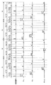
図2を参照する。図2には、本発明の液晶表示装置の駆動タイミングチャートが示されている。本発明を説明するにあたっては、フレームおよびサブフレームという用語を用いる。なお、1画面の表示を1フレームと呼び、1フレームは複数のサブフレームによって形成される。また、1フレームの表示を行うのに要する時間を1フレーム期間(Tf)と呼び、1フレーム期間(Tf)を複数に分割した期間をサブフレーム期間(Tsf)と呼ぶ。
【0031】
ここで説明する本発明の液晶表示装置においては、1フレームは2個のサブフレームによって形成されている。ここでは、1フレーム期間(Tf)は第1のサブフレーム期間(1st Tsf)および第2のサブフレーム期間(2nd Tsf)によって構成されている。
【0032】
まず、最初のフレーム期間の表示について説明する。第1のサブフレーム期間(1st Tsf)には、対応する画素TFTへ画像信号D1が供給され画像の表示が行われる。次に、第2のサブフレーム期間(2nd Tsf)には、対応する画素TFTへリセット信号Rが供給され、黒の表示が行われる。
【0033】
次のフレーム期間の表示も最初のフレーム期間の表示と同様に、第1のサブフレーム期間(1st Tsf)には、対応する画素TFTへ画像信号D2が供給され画像の表示が行われる。次に、第2のサブフレーム期間(2nd Tsf)には、対応する画素TFTへリセット信号Rが供給され、黒の表示が行われる。
【0034】
同様にして、連続するフレームの表示が行われ画像が形成される。
【0035】
このように、上述の本発明の液晶表示装置においては、1つのフレームを構成する2つのサブフレームのうち1個のサブフレームは、黒の表示が行われるので、画面の焼付きを防ぐことができる。
【0036】
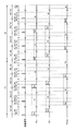
次に、図3を参照する。図3には、本発明の液晶表示装置の別の駆動タイミングチャートが示されている。
【0037】
ここで説明する本発明の液晶表示装置においては、1フレームは4個のサブフレームによって形成されている。ここでは、1フレーム期間(Tf)は第1のサブフレーム期間(1st Tsf)、第2のサブフレーム期間(2nd Tsf)、第3のサブフレーム期間(3rd Tsf)および第4のサブフレーム期間(4th Tsf)によって示す。
【0038】
まず、最初のフレーム期間の表示について説明する。第1のサブフレーム期間(1st Tsf)には、対応する画素TFTへ画像信号D1が供給され画像の表示が行われる。次に、第2のサブフレーム期間(2nd Tsf)には、対応する画素TFTへリセット信号Rが供給され、黒の表示が行われる。次に、第3のサブフレーム期間(3rd Tsf)には、対応する画素TFTへ第1のサブフレーム期間に供給された信号と同じ画像信号D1が供給され画像の表示が行われる。次に、第4のサブフレーム期間(4th Tsf)には、対応する画素TFTへリセット信号Rが供給され、黒の表示が行われる。
【0039】
この様に、本発明の液晶表示装置においては、同一フレーム期間中の各サブフレームにリセット信号以外の画像信号が供給される時には、同一の画像信号が供給されることになる。
【0040】
次のフレーム期間の表示も最初のフレーム期間の表示と同様に、第1のサブフレーム期間(1st Tsf)には、対応する画素TFTへ画像信号D2が供給され画像の表示が行われる。次に、第2のサブフレーム期間(2nd Tsf)には、対応する画素TFTへリセット信号Rが供給され、黒の表示が行われる。次に、第3のサブフレーム期間(3rd Tsf)には、対応する画素TFTへ第1のサブフレーム期間に供給された信号と同じ画像信号D2が供給され画像の表示が行われる。次に、第4のサブフレーム期間(4th Tsf)には、対応する画素TFTへリセット信号Rが供給され、黒の表示が行われる。
【0041】
同様にして、連続するフレームの表示が行われ画像が形成される。
【0042】
上述したように本発明の液晶表示装置においては、1つのフレームを構成する複数のサブフレームのうち少なくとも1個のサブフレームにはリセット信号が供給され黒の表示が行われるので、画面の焼付きを防ぐことができる。
【0043】
なお上述の例では、1フレームを2個のサブフレームによって形成した場合、および1フレームを4個のサブフレームによって形成した場合でかつ画像信号の供給とリセット信号の供給とを交互に行った場合について説明したが、本発明はこれらの場合に限られるわけではない。本発明の液晶表示装置においては、1フレームをn個のサブフレーム(1≦m<n、mは自然数)によって構成することができ、画像信号の供給とリセット信号の供給とを任意に設定してもよい。
【0044】
ここで、以下に本発明の液晶表示装置を実施例をもって更に詳しく説明する。ただし、本発明の液晶表示装置は、以下の実施例に限定されるわけではない。
【0045】
【実施例】
【0046】
(実施例1)
【0047】
図4を参照する。図4には、本実施例の液晶表示装置の概略構成図が示されている。101はデジタルドライバを有する液晶表示装置である。液晶表示装置101は、アクティブマトリクス基板101−1および対向基板101−2(図示せず)を有している。アクティブマトリクス基板101−1は、ソースドライバ101−1−1、ゲートドライバ101−1−2、デジタルビデオデータ分割回路101−1−3および複数の画素TFTがマトリクス状に配置された画素部101−1−4を有している。ソースドライバ101−1−1およびゲートドライバ101−1−2は画素部の複数の画素TFTを駆動する。また、対向基板101−2は対向電極101−2−1(図示せず)を有している。103−1および103−2は、FPC(Flexible Print Circuit)端子であり、これらのFPC端子に外部から種々の信号が入力される。
【0048】
次に図5を参照する。図5は本実施例の液晶表示装置のソースドライバを特に詳細に示した概略構成図である。101−1−1はソースドライバである。101−1−2はゲートドライバである。101−1−4は画素部である。101−1−3はデジタルビデオデータ分割回路(SPC;Serial-to-Parallel Conversion Circuit)である。
【0049】
ソースドライバ101−1−1は、シフトレジスタ回路(240ステージ×2のシフトレジスタ回路)501、ラッチ回路1(960×8デジタルラッチ回路)502、ラッチ回路2(960×8デジタルラッチ回路)503、セレクタ回路1(240のセレクタ回路)504、D/A変換回路(240のDAC)505、セレクタ回路2(240のセレクタ回路)506を有している。その他、バッファ回路やレベルシフタ回路(いずれも図示せず)を有している。また、説明の便宜上、D/A変換回路505にはレベルシフタ回路が含まれている。
【0050】
101−1−2はゲートドライバであり、シフトレジスタ回路、バッファ回路、レベルシフタ回路等(いずれも図示せず)を有している。
【0051】
画素部101−1−4は、1920×1080(横×縦)の画素を有している。各画素には画素TFTが配置されており、各画素TFTのソース領域にはソース信号線が、ゲート電極にはゲート信号線が電気的に接続されている。また、各画素TFTのドレイン領域には画素電極が電気的に接続されている。各画素TFTは、各画素TFTに電気的に接続された画素電極への画像信号(階調電圧)の供給を制御している。各画素電極に画像信号(階調電圧)が供給され、各画素電極と対向電極との間に挟まれた液晶に電圧が印加され液晶が駆動される。
【0052】
ここで、本実施例のアクティブマトリクス型液晶表示装置の動作および信号の流れを説明する。
【0053】
まず、ソースドライバの動作を説明する。シフトレジスタ回路501にクロック信号(CK)およびスタートパルス(SP)が入力される。シフトレジスタ回路501は、これらのクロック信号(CK)およびスタートパルス(SP)に基づきタイミング信号を順に発生させ、バッファ回路等(図示せず)を通して後段の回路へタイミング信号を順次供給する。
【0054】
シフトレジスタ回路501からのタイミング信号は、バッファ回路等によってバッファされる。タイミング信号が供給されるソース信号線には、多くの回路あるいは素子が接続されているために負荷容量(寄生容量)が大きい。この負荷容量が大きいために生ずるタイミング信号の立ち上がりの”鈍り”を防ぐために、このバッファ回路が設けられる。
【0055】
バッファ回路によってバッファされたタイミング信号は、ラッチ回路1(502)に供給される。ラッチ回路1(502)は、8ビットデジタルビデオデータ(8bit digital video data)を処理するラッチ回路を960ステージ有してる。ラッチ回路1(502)は、前記タイミング信号が入力されると、デジタルビデオデータ分割回路101−1−3から供給される8ビットデジタルビデオデータを順次取り込み、保持する。
【0056】
ラッチ回路1(502)の全てのステージにラッチ回路にデジタルビデオデータの書き込みが一通り終了するまでの時間は、ライン期間と呼ばれる。すなわち、ラッチ回路1(502)の中で一番左側のステージのラッチ回路にデジタルビデオデータの書き込みが開始される時点から、一番右側のステージのラッチ回路にデジタルビデオデータの書き込みが終了する時点までの時間間隔がライン期間である。実際には、上記ライン期間に水平帰線期間が加えられた期間をライン期間と呼ぶこともある。
【0057】
1ライン期間の終了後、シフトレジスタ回路501の動作タイミングに合わせて、ラッチ回路2(503)にラッチシグナル(Latch Signal)が供給される。この瞬間、ラッチ回路1(502)に書き込まれ保持されているデジタルビデオデータは、ラッチ回路2(503)に一斉に送出され、ラッチ回路2(503)の全ステージのラッチ回路に書き込まれ、保持される。
【0058】
デジタルビデオデータをラッチ回路2(503)に送出し終えたラッチ回路1(502)には、シフトレジスタ回路501からのタイミング信号に基づき、再びデジタルビデオデータ分割回路から供給されるデジタルビデオデータの書き込みが順次行われる。
【0059】
この2順目の1ライン期間中には、ラッチ回路2(503)に書き込まれ、保持されているデジタルビデオデータが、セレクタ回路1(504)によって順次選択され、D/A変換回路505に供給される。なお本実施例では、セレクタ回路1(504)においては、1つのセレクタ回路がソース信号線4本に対応している。
【0060】
なお、セレクタ回路については、本出願人による特許出願である特願平9−286098号に記載されているものを用いることもできる。
【0061】
セレクタ回路504で選択されたラッチ回路2(503)からの8ビット・デジタルビデオデータがD/A変換回路505に供給される。ここで、本実施例に用いられるD/A変換回路について図7を用いて説明する。
【0062】
図7には、本実施例のD/A変換回路の回路図が示されている。なお、本実施例のD/A変換回路は、レベルシフタ回路(L.S)505−2を有しているが、このレベルシフタ回路を省略して設計することも可能である。レベルシフタ回路においては、入力INに信号Loが入力され、入力INbに信号Hiが入力された時に、出力OUTからは高電位電源VddHIが、出力OUTbからは低電位電源Vssが出力されるようになっている。また、入力INに信号Hiが入力され、入力INbに信号Loが入力された時に、出力OUTからは高電位電源Vssが、出力OUTbからは低電位電源VddHIが出力されるようになっている。
【0063】
本実施例のD/A変換回路には、NOR回路(505−1)の一方の入力にデジタルビデオデータA0〜A7の反転データ(ここでは反転A0〜反転A7と呼ぶ)が入力されるようになっている。このNOR回路(505−1)の他方の入力には、リセットパルスA(ResA)が入力される。このリセットパルスAは、D/A変換回路のリセット期間TRに入力される。本実施例の場合、デジタルビデオデータ(反転A0〜A7)はリセット期間TR中にもNOR回路(505−1)へ入力されるが、NOR回路にリセットパルスResAが入力されている間は、NOR回路からはデジタルビデオデータが出力されないようになっている。
【0064】
なお、NOR回路を省略し、リセット期間TRの終了後、デジタルビデオデータ(反転A0〜A7)が入力されるようにしてもよい。
【0065】
リセット期間TRの終了後、データ書き込み期間TEが始まり、8ビットのデジタルビデオデータがレベルシフタ回路によってその電圧レベルを上げられ、スイッチ回路SW0〜SW7に入力される。
【0066】
スイッチ回路SW0〜SW7は、それぞれ2個のアナログスイッチASW1およびASW2によって構成されている。ASW1の一端はDC_VIDEO_Lに、その他端はASW2の一端に接続されかつ容量に接続されている。また、各ASW2の一端はDC_VIDEO_Hに、その他端はASW1の一端に接続されかつ容量(1pF、2pF、4pF、8pF、1pF、2pF、4pF、8pF)に接続されている。各容量の一端は2つのアナログスイッチに接続されており、他端はリセットスイッチ2(Res2)に接続されている。また、リセットスイッチ1(Res1)の一端は、DC_VIDEO_Mに接続されており、他端は上位ビットに対応する容量の一端に接続されている。リセットスイッチRes1およびRes2には、リセットパルス(ResB)および反転リセットパルス(反転ResB)が入力される。
【0067】
また、上位ビットに対応する回路と下位ビットに対応する回路の接続点には、容量(1pF)が設けられている。なお、本実施例における、上述の全て容量はそれらの値に限定されるわけではない。
【0068】
D/A変換回路505は、8ビットのデジタルビデオデータを画像信号(階調電圧)に変換し、セレクタ回路2(506)によって選択されるソース信号線に順次供給される。
【0069】
ソース信号線に供給される画像信号は、ソース信号線に接続されている画素部の画素TFTのソース領域に供給される。
【0070】
ゲートドライバ101−1−2においては、シフトレジスタ(図示せず)からのタイミング信号(走査信号)がバッファ回路(図示せず)に供給され、対応するゲート信号線(走査線)に供給される。ゲート信号線には、1ライン分の画素TFTのゲート電極が接続されており、1ライン分全ての画素TFTを同時にONにしなくてはならないので、バッファ回路には電流容量の大きなものが用いられる。
【0071】
このように、ゲートドライバからの走査信号によって対応する画素TFTのスイッチングが行われ、ソースドライバからの画像信号(階調電圧)が画素TFTに供給され、液晶分子が駆動される。
【0072】
101−1−3はデジタルビデオデータ分割回路(SPC;Serial-to-Parallel Conversion Circuit)である。デジタルビデオデータ分割回路101−1−3は、外部から入力されるデジタルビデオデータの周波数を1/xに落とすための回路である(xは2以上の自然数)。外部から入力されるデジタルビデオデータを分割することにより、駆動回路の動作に必要な信号の周波数も1/xに落とすことができる。
【0073】
ここで、本実施例の液晶表示装置101の回路構成、特に画素部101−1−4の構成について、図6を用いて説明する。
【0074】
本実施例においては、画素部101−1−4は、(1920×1080)個の画素を有している。それぞれの画素には、説明の便宜上、P1,1、P2,1、・・・、P1079,1919等の符号が付けられている。また、それぞれの画素は、画素TFT601、保持容量603を有している。アクティブマトリクス基板と対向基板との間には液晶が挟まれており、液晶602は各画素に対応する液晶を模式的に示したものである。なお、COMはコモン電圧端子であり、対向電極および保持容量の一端に接続されている。
【0075】
本実施例の液晶表示装置は、1ライン分の画素(例えば、P1,1、P1,2、・・・、およびP1,1919)を同時に駆動する、いわゆる線順次駆動を行う。言い換えると、1ライン分の全ての画素に同時に画像進号を書き込む。
【0076】
ここで、本実施例の液晶表示装置の表示方法について説明する。図8を参照する。図8には、本実施例の液晶表示装置の駆動タイミングチャートが示されている。ここで説明する本発明の液晶表示装置においては、1フレームは2個のサブフレームによって形成されている。ここでは、1フレーム期間(Tf)は第1のサブフレーム期間(1st Tsf)および第2のサブフレーム期間(2nd Tsf)によって構成されている。
【0077】
図8には、画素P1,1、画素P2,1、および画素P1079,1が例にとって示されている。
【0078】
まず、最初のフレーム期間の表示について説明する。第1のサブフレーム期間(1st Tsf)にゲートドライバに走査信号が入力され、第1のサブフレームライン期間(1st Tsfl)に画素P1,1〜画素P1,1919にデジタルビデオデータがD/A変換回路によって画像信号に変換され書き込まれる。その後、次のサブフレームライン期間には、画素P2,1〜画素P2,1919にデジタルビデオデータがD/A変換回路によって画像信号に変換され書き込まれる。その後、各画素に順に画像信号が書き込まれ、最後の1ライン分の画素P1079,1〜画素P1079,1919に画像信号が書き込まれ、第1のサブフレーム期間が終了する。
【0079】
つぎに、第2のサブフレーム期間(2nd Tsf)が始まる。第2のサブフレーム期間(2nd Tsf)にゲートドライバに走査信号が入力され、第2のサブフレームライン期間(2nd Tsfl)に画素P1,1〜画素P1,1919にデジタルビデオデータがD/A変換回路によって変換されたリセット信号が書き込まれ、黒の表示が行われる。その後、次のサブフレームライン期間には、画素P2,1〜画素P2,1919にデジタルビデオデータがD/A変換回路によって変換されたリセット信号が書き込まれ、黒の表示が行われる。その後、各画素に順にリセット信号が書き込まれ、最後の1ライン分の画素P1079,1〜画素P1079,1919にリセット信号が書き込まれ、黒の表示が行われる。こうして第2のサブフレーム期間が終了する。
【0080】
次のフレーム期間の表示も最初のフレーム期間の表示と同様に、第1のサブフレーム期間(1st Tsf)には、対応する画素TFTへ画像信号D2が供給され画像の表示が行われる。次に、第2のサブフレーム期間(2nd Tsf)には、対応する画素TFTへリセット信号Rが供給され、黒の表示が行われる。
【0081】
同様にして、連続するフレームの表示が行われ画像が形成される。
【0082】
このように、上述の本発明の液晶表示装置においては、1つのフレームを構成する2つのサブフレームのうち1個のサブフレームは、黒の表示が行われるので、画面の焼付きを防ぐことができる。
【0083】
(実施例2)
【0084】
本実施例では、上述の実施例1とは異なる表示方法による本発明の液晶表示装置について説明する。なお、本実施例の液晶表示装置の構成は、実施例1と同様であるので、実施例1を参照できる。
【0085】
本実施例の液晶表示装置の表示方法について説明する。図9を参照する。図9には、本実施例の液晶表示装置の駆動タイミングチャートが示されている。ここで説明する本発明の液晶表示装置においては、1フレームは4個のサブフレームによって形成されている。ここでは、1フレーム期間(Tf)は第1のサブフレーム期間(1st Tsf)、第2のサブフレーム期間(2nd Tsf)、第3のサブフレーム期間(3rd Tsf)および第4のサブフレーム期間(4th Tsf)によって構成されている。
【0086】
図9には、画素P1,1、画素P2,1、および画素P1079,1が例にとって示されている。
【0087】
まず、最初のフレーム期間の表示について説明する。第1のサブフレーム期間(1st Tsf)にゲートドライバに走査信号が入力され、第1のサブフレームライン期間(1st Tsfl)に画素P1,1〜画素P1,1919にデジタルビデオデータがD/A変換回路によって画像信号に変換され書き込まれる。図9に示される画素P1,1には画像信号D1が書き込まれる。その後、次のサブフレームライン期間には、画素P2,1〜画素P2,1919にデジタルビデオデータがD/A変換回路によって画像信号に変換され書き込まれる。図9に示される画素P2,1には画像信号D3が書き込まれる。その後、各画素に順に画像信号が書き込まれ、最後の1ライン分の画素P1079,1〜画素P1079,1919に画像信号が書き込まれる。図9に示される画素P1079,1には画像信号D5が書き込まれる。こうして第1のサブフレーム期間が終了する。
【0088】
つぎに、第2のサブフレーム期間(2nd Tsf)が始まる。第2のサブフレーム期間(2nd Tsf)にゲートドライバに走査信号が入力され、第2のサブフレームライン期間(2nd Tsfl)に画素P1,1〜画素P1,1919にデジタルビデオデータがD/A変換回路によって変換されたリセット信号が書き込まれ、黒の表示が行われる。その後、次のサブフレームライン期間には、画素P2,1〜画素P2,1919にデジタルビデオデータがD/A変換回路によって変換されたリセット信号が書き込まれ、黒の表示が行われる。その後、各画素に順にリセット信号が書き込まれ、最後の1ライン分の画素P1079,1〜画素P1079,1919にリセット信号が書き込まれ、黒の表示が行われる。こうして第2のサブフレーム期間が終了する。
【0089】
次に、第3のサブフレーム期間(3rd Tsf)が始まる。第3のサブフレーム期間(3rd Tsf)にゲートドライバに走査信号が入力され、第3のサブフレームライン期間(3rd Tsfl)に画素P1,1〜画素P1,1919にデジタルビデオデータがD/A変換回路によって画像信号に変換され書き込まれる。図9に示される画素P1,1には第1のサブフレーム期間と同じ画像信号D1が書き込まれる。その後、次のサブフレームライン期間には、画素P2,1〜画素P2,1919にデジタルビデオデータがD/A変換回路によって画像信号に変換され書き込まれる。図9に示される画素P2,1には第1のサブフレーム期間と同じ画像信号D3が書き込まれる。その後、各画素に順に画像信号が書き込まれ、最後の1ライン分の画素P1079,1〜画素P1079,1919に画像信号が書き込まれる。図9に示される画素P1079,1には第1のサブフレーム期間と同じ画像信号D5が書き込まれる。こうして第1のサブフレーム期間が終了する。
【0090】
つぎに、第4のサブフレーム期間(4th Tsf)が始まる。第4のサブフレーム期間(4th Tsf)にゲートドライバに走査信号が入力され、第4のサブフレームライン期間(4th Tsfl)に画素P1,1〜画素P1,1919にデジタルビデオデータがD/A変換回路によって変換されたリセット信号が書き込まれ、黒の表示が行われる。その後、次のサブフレームライン期間には、画素P2,1〜画素P2,1919にデジタルビデオデータがD/A変換回路によって変換されたリセット信号が書き込まれ、黒の表示が行われる。その後、各画素に順にリセット信号が書き込まれ、最後の1ライン分の画素P1079,1〜画素P1079,1919にリセット信号が書き込まれ、黒の表示が行われる。こうして第4のサブフレーム期間が終了する。
【0091】
こうして最初のフレーム期間が終了する。その後、次のフレーム期間が始まり第1〜第4のサブフレームの表示が行われる。
【0092】
同様にして、連続するフレームの表示が行われ画像が形成される。
【0093】
このように、上述の本発明の液晶表示装置においては、1個のフレームを構成する4個のサブフレームのうち2個のサブフレームは、黒の表示が行われるので、画面の焼付きを防ぐことができる。
【0094】
(実施例3)
【0095】
図10を参照する。図10には、本実施例の液晶表示装置の概略構成図が示されている。1001はデジタルドライバを有する液晶表示装置である。液晶表示装置1001は、アクティブマトリクス基板1001−1および対向基板1001−2(図示せず)を有している。アクティブマトリクス基板1001−1は、ソースドライバ1001−1−1、ソースドライバ1001−1−2、ゲートドライバ1001−1−3、デジタルビデオデータ分割回路1001−1−4および複数の画素TFTがマトリクス状に配置された画素部1001−1−5を有している。ソースドライバ1001−1−1、ソースドライバ1001−1−2およびゲートドライバ1001−1−3は画素部の複数の画素TFTを駆動する。また、対向基板1001−2は対向電極1001−2−1(図示せず)を有している。1003−1および1003−2は、FPC端子であり、これらのFPC端子に外部から種々の信号が入力される。
【0096】
ソースドライバ1001−1−1は画素部の奇数番目のソース信号線に接続された画素を駆動し、ソースドライバ1001−1−2は画素部の偶数番目のソース信号線に接続された画素を駆動する。
【0097】
他の構成は、実施例1と同じである。
【0098】
(実施例4)
【0099】
図22を参照する。図22には、本実施例の液晶表示装置の駆動タイミングチャートが示されている。本発明を説明するにあたっては、フレームおよびサブフレームという用語を用いる。1画面の表示を1フレームと呼び、1フレームは複数のサブフレームによって形成される。また、1フレームの表示を行うのに要する時間を1フレーム期間(Tf)と呼び、1フレーム期間(Tf)を構成する複数のサブフレームの表示に対応する期間をサブフレーム期間(Tsf)と呼ぶ。
【0100】
本発明の液晶表示装置においては、複数のサブフレームを高速に表示することによって1画面の表示を行う。あるフレームを表示する際に、あるサブフレームの表示を行うための画像信号と、その次のサブフレームの表示を行うための画像信号は、基準電位からの絶対値が同じで、反対極性である。本発明の液晶表示装置においては、これら2つのサブフレームは常に対になって表示される。
【0101】
上述の動作に加えて、複数のサブフレームの表示のうち少なくとも1つのサブフレームには、リセット信号が印加される。本願明細書においては、リセット信号とは、画面にほぼ黒の表示を行うための信号をいうものとする。
【0102】
以下に説明する本発明の液晶表示装置においては、1フレームは3個のサブフレームによって形成されている。ここでは、1フレーム期間(Tf)は第1のサブフレーム期間(1st Tsf)、第2のサブフレーム期間(2nd Tsf)および第3のサブフレーム期間(3rd Tsf)によって構成されている。
【0103】
まず最初のフレーム期間の表示について説明する。第1のサブフレーム期間(1st Tsf)には、対応する画素TFTへ画像信号(D1)が供給され、液晶分子が駆動され画像の表示が行われる。次に、第2のサブフレーム期間(2nd Tsf)には、対応する画素TFTへ画像信号(D1)と絶対値が同じで反対極性の画像信号(反転D1)が供給され画像の表示が行われる。次に、第3のサブフレーム期間には、対応する画素TFTへリセット信号(R)が供給され、黒の画像表示が行われる。このリセット信号は、画像信号の基準電位となっている電位を供給するものであってもよい。また、基準電位以外の電位であっても、黒の画像表示を行う信号であればよい。
【0104】
以上の動作によって最初のフレーム期間の表示が終了し、次のフレーム期間が始まる。次のフレーム期間の表示も最初のフレーム期間の表示と同様に行われる。第1のサブフレーム期間(1st Tsf)には、対応する画素TFTへ画像信号(D2)が供給され画像の表示が行われる。次に、第2のサブフレーム期間(2nd Tsf)には、対応する画素TFTへ画像信号(D2)と絶対値が同じで反対極性の画像信号(反転D2)が供給され画像の表示が行われる。次に、第3のサブフレーム期間には、対応する画素TFTへリセット信号(R)が供給され、黒の画像表示が行われる。
【0105】
同様にして、連続するフレームの表示が行われ画像が形成される。
【0106】
上述ように、本発明の液晶表示装置においては、連続するサブフレームに絶対値が等しく反対極性の画像信号が同じ画素TFTに供給されるので、画像信号が液晶分子に供給された時に蓄積される液晶分子の自発分極と反対極性の電荷がキャンセルされる。かつ、すくなくとも1つのサブフレームには、ほぼ黒の画像表示が行われる。よって、表示の「焼付き」を防止することができる。
【0107】
なお上述の例では、1フレームを3個のサブフレームによって形成した場合について説明したが、本発明はこれらの場合に限られるわけではない。本発明の液晶表示装置においては、1フレームをm個のサブフレームによって形成し、少なくともn個のサブフレームにリセット信号を供給するようにしてもよい(m>n、mおよびnは自然数)。
【0108】
図23を参照する。図23には、本実施例の液晶表示装置の概略構成図が示されている。7101はデジタルドライバを有する液晶表示装置である。液晶表示装置7101は、アクティブマトリクス基板7101−1および対向基板7101−2(図示せず)を有している。アクティブマトリクス基板7101−1は、ソースドライバ7101−1−1、ゲートドライバ7101−1−2および複数の画素TFTがマトリクス状に配置された画素部7101−1−3を有している。ソースドライバ7101−1−1およびゲートドライバ7101−1−2は画素部の複数の画素TFTを駆動する。また、対向基板7101−2は対向電極7101−2−1(図示せず)を有している。7103−1および7103−2は、FPC(Flexible Print Circuit)端子であり、これらのFPC端子に外部から種々の信号が入力される。なお、本実施例の液晶表示装置には、外部から8ビットデジタルデータが入力される。
【0109】
次に図24を参照する。図24は本実施例の液晶表示装置のソースドライバを特に詳細に示した概略構成図である。7101−1−1はソースドライバである。7101−1−2はゲートドライバである。7101−1−3は画素部である。
【0110】
ソースドライバ7101−1−1は、シフトレジスタ回路7501、ラッチ回路1(7502)、ラッチ回路2(7503)およびD/A変換回路7504を有している。その他、バッファ回路やレベルシフタ回路(いずれも図示せず)を有している。また、説明の便宜上、D/A変換回路7504にはレベルシフタ回路が含まれている。
【0111】
7101−1−2はゲートドライバであり、シフトレジスタ回路、バッファ回路、レベルシフタ回路等(いずれも図示せず)を有している。
【0112】
画素部7101−1−3は、1920×1080(横×縦)の画素を有している。各画素には画素TFTが配置されており、各画素TFTのソース領域にはソース信号線が、ゲート電極にはゲート信号線が電気的に接続されている。また、各画素TFTのドレイン領域には画素電極が電気的に接続されている。各画素TFTは、各画素TFTに電気的に接続された画素電極への画像信号(階調電圧)の供給を制御している。各画素電極に画像信号(階調電圧)が供給され、各画素電極と対向電極との間に挟まれた液晶に電圧が印加され液晶が駆動される。
【0113】
ここで、本実施例のアクティブマトリクス型液晶表示装置の動作および信号の流れを説明する。
【0114】
まず、ソースドライバの動作を説明する。シフトレジスタ回路7501にクロック信号(CK)およびスタートパルス(SP)が入力される。シフトレジスタ回路7501は、これらのクロック信号(CK)およびスタートパルス(SP)に基づきタイミング信号を順に発生させ、バッファ回路等(図示せず)を通して後段の回路へタイミング信号を順次供給する。
【0115】
シフトレジスタ回路7501からのタイミング信号は、バッファ回路等によってバッファされる。タイミング信号が供給されるソース信号線には、多くの回路あるいは素子が接続されているために負荷容量(寄生容量)が大きい。この負荷容量が大きいために生ずるタイミング信号の立ち上がりの”鈍り”を防ぐために、このバッファ回路が設けられる。
【0116】
バッファ回路によってバッファされたタイミング信号は、ラッチ回路1(7502)に供給される。ラッチ回路1(7502)は、前記タイミング信号が入力されると、外部から供給される8ビットデジタルビデオデータを順次取り込み、保持する。
【0117】
ラッチ回路1(7502)の全てのステージにラッチ回路にデジタルビデオデータの書き込みが一通り終了するまでの時間は、サブフレームライン期間である。すなわち、ラッチ回路1(7502)の中で一番左側のステージのラッチ回路にデジタルビデオデータの書き込みが開始される時点から、一番右側のステージのラッチ回路にデジタルビデオデータの書き込みが終了する時点までの時間間隔がサブフレームライン期間である。実際には、このサブフレームライン期間に水平帰線期間が加えられた期間をサブフレームライン期間と呼ぶこともある。
【0118】
1サブフレームライン期間の終了後、シフトレジスタ回路7501の動作タイミングに合わせて、ラッチ回路2(7503)にラッチシグナル(Latch Signal)が供給される。この瞬間、ラッチ回路1(7502)に書き込まれ保持されているデジタルビデオデータは、ラッチ回路2(7503)に一斉に送出され、ラッチ回路2(7503)の全ステージのラッチ回路に書き込まれ、保持される。
【0119】
デジタルビデオデータをラッチ回路2(7503)に送出し終えたラッチ回路1(7502)には、シフトレジスタ回路7501からのタイミング信号に基づき、外部から供給されるデジタルビデオデータの書き込みが順次行われる。
【0120】
この2順目の1サブフレームライン期間中には、ラッチ回路2(7503)に書き込まれ、保持されているデジタルビデオデータがD/A変換回路7504に供給される。
【0121】
なお、本実施例に用いられるD/A変換回路7504は、上述の実施例1の図7に示されるものと同様のものが用いられてもよい。
【0122】
ここで、本実施例の液晶表示装置の液晶表示装置7101の回路構成、特に画素部7101−1−3の構成について、図25を用いて説明する。
【0123】
本実施例においては、画素部7101−1−3は、(1920×1080)個の画素を有している。それぞれの画素には、説明の便宜上、P1,1、P2,1、・・・、P1079,1919等の符号が付けられている。また、それぞれの画素は、画素TFT7601、保持容量7603を有している。アクティブマトリクス基板と対向基板との間には液晶が挟まれており、液晶7602は各画素に対応する液晶を模式的に示したものである。なお、COMはコモン電圧端子であり、対向電極および保持容量の一端に接続されている。
【0124】
本実施例の液晶表示装置は、1ライン分の画素(例えば、P1,1、P1,2、・・・、およびP1,1919)を同時に駆動する、いわゆる線順次駆動を行う。言い換えると、1ライン分の全ての画素に同時に画像信号を書き込む。
【0125】
ここで、本実施例の液晶表示装置の表示方法について説明する。図26を参照する。図26には、本実施例の液晶表示装置の駆動タイミングチャートが示されている。ここで説明する本発明の液晶表示装置においては、1フレームは3個のサブフレームによって形成されている。本実施例では、1フレーム期間(Tf)は第1のサブフレーム期間(1st Tsf)、第2のサブフレーム期間(2nd Tsf)および第3のサブフレーム期間(3rd Tsf)によって構成されている。
【0126】
図26には、画素P1,1、画素P2,1、および画素P1079,1が例にとって示されている。
【0127】
まず、最初のフレーム期間の表示について説明する。第1のサブフレーム期間(1st Tsf)にゲートドライバにスタートパルスが入力され、第1のサブフレームライン期間(1st Tsfl)に画素P1,1〜画素P1,1919にデジタルビデオデータがD/A変換回路によって画像信号に変換され書き込まれる。図26に示すように、例えば、画素P1,1には画像信号(D1)が書き込まれる。
【0128】
その後、次のサブフレームライン期間には、画素P2,1〜画素P2,1919にデジタルビデオデータがD/A変換回路によって画像信号に変換され書き込まれる。図26に示すように、例えば、画素P2,1には画像信号(D4)が書き込まれる。
【0129】
その後、各画素に順に画像信号が書き込まれ、最後の1ライン分の画素P1079,1〜画素P1079,1919に画像信号が書き込まれ、第1のサブフレーム期間が終了する。なお、図26に示すように、例えば、画素P1079,1には画像信号(D7)が書き込まれる。
【0130】
次に第2のサブフレーム期間(2nd Tsf)が始まる。第2のサブフレーム期間(2nd Tsf)の開始時にゲートドライバにスタートパルスが入力され、第2のサブフレームライン期間(2nd Tsfl)に画素P1,1〜画素P1,1919にデジタルビデオデータがD/A変換回路によって画像信号に変換され書き込まれる。図26に示すように、例えば、画素P1,1には画像信号(反転D1)が書き込まれる。
【0131】
その後、次のサブフレームライン期間には、画素P2,1〜画素P2,1919にデジタルビデオデータがD/A変換回路によって画像信号に変換され書き込まれる。図26に示すように、例えば、画素P2,1には画像信号(反転D4)が書き込まれる。
【0132】
その後、各画素に順に画像信号が書き込まれ、最後の1ライン分の画素P1079,1〜画素P1079,1919に画像信号が書き込まれ、第1のサブフレーム期間が終了する。図26に示すように、例えば、画素P1079,1には画像信号(反転D7)が書き込まれる。
【0133】
つぎに、第3のサブフレーム期間(3rd Tsf)が始まる。第3のサブフレーム期間(3rd Tsf)の開始時にゲートドライバにスタートパルスが入力され、画素P1,1〜画素P1,1919にデジタルビデオデータがD/A変換回路によって変換されたリセット信号(R)が書き込まれ、黒の画像表示が行われる。その後、次のサブフレームライン期間には、画素P2,1〜画素P2,1919にデジタルビデオデータがD/A変換回路によって変換されたリセット信号(R)が書き込まれ、黒の画像表示が行われる。その後、各画素に順にリセット信号(R)が書き込まれ、最後の1ライン分の画素P1079,1〜画素P1079,1919にリセット信号(R)が書き込まれ、黒の画像表示が行われる。こうして第3のサブフレーム期間が終了する。
【0134】
以上の動作をもって1フレームの画像表示が終了する。
【0135】
同様にして、連続するフレームの表示が行われ画像が形成される。
【0136】
上述ように、本実施例の液晶表示装置においては、連続するサブフレームに絶対値が同じで反対極性の画像信号が同じ画素TFTに供給されるので、画像信号が液晶分子に供給された時に蓄積される液晶分子の自発分極と反対極性の電荷がキャンセルされる。かつ、すくなくとも1つのサブフレームには、黒の表示が行われる。よって、表示の「焼付き」を防止することができる。
【0137】
(実施例5)
【0138】
本実施例では、上述の実施例4とは異なる表示方法による本発明の液晶表示装置について説明する。なお、本実施例の液晶表示装置の構成は、実施例4と同様であるので、実施例4を参照できる。
【0139】
ここで、本実施例の液晶表示装置の表示方法について説明する。図27を参照する。図27には、本実施例の液晶表示装置の駆動タイミングチャートが示されている。ここで説明する本発明の液晶表示装置においては、1フレームは5個のサブフレームによって形成されている。つまり本実施例では、1フレーム期間(Tf)は第1のサブフレーム期間(1st Tsf)、第2のサブフレーム期間(2nd Tsf)、第3のサブフレーム期間(3rd Tsf)、第4のサブフレーム期間(4th Tsf)および第5のサブフレーム期間(5th Tsf)によって構成されている。
【0140】
図27には、画素P1,1、画素P2,1、および画素P1079,1が例にとって示されている。
【0141】
まず、最初のフレーム期間の表示について説明する。第1のサブフレーム期間(1st Tsf)にゲートドライバにスタートパルスが入力され、第1のサブフレームライン期間(1st Tsfl)に画素P1,1〜画素P1,1919にデジタルビデオデータがD/A変換回路によって画像信号に変換され書き込まれる。図27に示すように、例えば、画素P1,1には画像信号(D1)が書き込まれる。
【0142】
その後、次のサブフレームライン期間には、画素P2,1〜画素P2,1919にデジタルビデオデータがD/A変換回路によって画像信号に変換され書き込まれる。図27に示すように、例えば、画素P2,1には画像信号(D3)が書き込まれる。
【0143】
その後、各画素に順に画像信号が書き込まれ、最後の1ライン分の画素P1079,1〜画素P1079,1919に画像信号が書き込まれ、第1のサブフレーム期間が終了する。なお、図27に示すように、例えば、画素P1079,1には画像信号(D5)が書き込まれる。
【0144】
次に第2のサブフレーム期間(2nd Tsf)が始まる。第2のサブフレーム期間(2nd Tsf)の開始時にゲートドライバにスタートパルスが入力され、第2のサブフレームライン期間(2nd Tsfl)に画素P1,1〜画素P1,1919にデジタルビデオデータがD/A変換回路によって画像信号に変換され書き込まれる。図27に示すように、例えば、画素P1,1には画像信号(反転D1)が書き込まれる。
【0145】
その後、次のサブフレームライン期間には、画素P2,1〜画素P2,1979にデジタルビデオデータがD/A変換回路によって画像信号に変換され書き込まれる。図27に示すように、例えば、画素P2,1には画像信号(反転D3)が書き込まれる。
【0146】
その後、各画素に順に画像信号が書き込まれ、最後の1ライン分の画素P1079,1〜画素P1079,1919に画像信号が書き込まれ、第2のサブフレーム期間が終了する。図27に示すように、例えば、画素P1079,1には画像信号(反転D5)が書き込まれる。
【0147】
次に第3のサブフレーム期間(3rd Tsf)が始まる。第3のサブフレーム期間(3rd Tsf)の開始時にゲートドライバにスタートパルスが入力され、第3のサブフレームライン期間(3rd Tsfl)に画素P1,1〜画素P1,1919にデジタルビデオデータがD/A変換回路によって画像信号に変換され書き込まれる。図27に示すように、例えば、画素P1,1には第1のサブフレームライン期間(1st Tsfl)に書き込まれた画像信号と同じ画像信号(D1)が書き込まれる。
【0148】
その後、次のサブフレームライン期間には、画素P2,1〜画素P2,1919にデジタルビデオデータがD/A変換回路によって画像信号に変換され書き込まれる。図27に示すように、例えば、画素P2,1には第1のサブフレームライン期間(1st Tsfl)に書き込まれた画像信号と同じ画像信号(D3)が書き込まれる。
【0149】
その後、各画素に順に画像信号が書き込まれ、最後の1ライン分の画素P1079,1〜画素P1079,1919に画像信号が書き込まれ、第3のサブフレーム期間が終了する。図27に示すように、例えば、画素P1079,1には第1のサブフレームライン期間(1st Tsfl)に書き込まれた画像信号と同じ画像信号(D5)が書き込まれる。
【0150】
次に第4のサブフレーム期間(4th Tsf)が始まる。第4のサブフレーム期間(4th Tsf)の開始時にゲートドライバにスタートパルスが入力され、第4のサブフレームライン期間(4th Tsfl)に画素P1,1〜画素P1,1919にデジタルビデオデータがD/A変換回路によって画像信号に変換され書き込まれる。図27に示すように、例えば、画素P1,1には第2のサブフレームライン期間(2nd Tsfl)に書き込まれた画像信号と同じ画像信号(反転D1)が書き込まれる。
【0151】
その後、次のサブフレームライン期間には、画素P2,1〜画素P2,1919にデジタルビデオデータがD/A変換回路によって画像信号に変換され書き込まれる。図27に示すように、例えば、画素P2,1には第2のサブフレームライン期間(1st Tsfl)に書き込まれた画像信号と同じ画像信号(反転D3)が書き込まれる。
【0152】
その後、各画素に順に画像信号が書き込まれ、最後の1ライン分の画素P1079,1〜画素P1079,1919に画像信号が書き込まれ、第4のサブフレーム期間が終了する。図27に示すように、例えば、画素P1079,1には第2のサブフレームライン期間(2nd Tsfl)に書き込まれた画像信号と同じ画像信号(反転D5)が書き込まれる。
【0153】
つぎに、第5のサブフレーム期間(5th Tsf)が始まる。第5のサブフレーム期間(5th Tsf)の開始時にゲートドライバにスタートパルスが入力され、第5のサブフレームライン期間(5th Tsfl)に画素P1,1〜画素P1,1919にデジタルビデオデータがD/A変換回路によって変換されたリセット信号(R)が書き込まれ、黒の画像表示が行われる。その後、次のサブフレームライン期間には、画素P2,1〜画素P2,1919にデジタルビデオデータがD/A変換回路によって変換されたリセット信号(R)が書き込まれ、黒の画像表示が行われる。その後、各画素に順にリセット信号(R)が書き込まれ、最後の1ライン分の画素P1079,1〜画素P1079,1919にリセット信号(R)が書き込まれ、黒の画像表示が行われる。こうして第5のサブフレーム期間が終了する。
【0154】
こうして第1〜第5のサブフレーム期間が終了し、1つのフレーム期間が終了する。
【0155】
同様にして、連続するフレームの表示が行われ画像が形成される。
【0156】
上述のように本実施例の液晶表示装置においては、1フレームの表示を5個のサブフレームの表示を高速に行うことによって形成する。よって、表示の「焼付き」を防止することができ、かつ画像のチラツキも少なくすることができる。
【0157】
(実施例6)
【0158】
図28を参照する。図28には、本実施例の液晶表示装置の概略構成図が示されている。8001はデジタルドライバを有する液晶表示装置である。液晶表示装置8001は、アクティブマトリクス基板8001−1および対向基板8001−2(図示せず)を有している。アクティブマトリクス基板8001−1は、ソースドライバ8001−1−1、ソースドライバ8001−1−2、ゲートドライバ8001−1−3、デジタルビデオデータ分割回路8001−1−4および複数の画素TFTがマトリクス状に配置された画素部8001−1−5を有している。ソースドライバ8001−1−1、ソースドライバ8001−1−2およびゲートドライバ8001−1−3は画素部の複数の画素TFTを駆動する。また、対向基板8001−2は対向電極8001−2−1(図示せず)を有している。8003−1および8003−2は、FPC端子であり、これらのFPC端子に外部から種々の信号が入力される。
【0159】
ソースドライバ8001−1−1は画素部の奇数番目のソース信号線に接続された画素を駆動し、ソースドライバ8001−1−2は画素部の偶数番目のソース信号線に接続された画素を駆動する。
【0160】
8001−1−4はデジタルビデオデータ分割回路(SPC;Serial-to-Parallel Conversion Circuitと呼ぶこともある)である。デジタルビデオデータ分割回路8001−1−4は、外部から入力されるデジタルビデオデータの周波数を1/xに落とすための回路である(xは2以上の自然数)。外部から入力されるデジタルビデオデータを分割することにより、駆動回路の動作に必要な信号の周波数も1/xに落とすことができる。本実施例の液晶表示装置においては、デジタルビデオデータ分割回路8001−1−4は、外部から入力される80MHzの8ビットデジタルビデオデータを10MHzに落とす。
【0161】
他の構成は、実施例4と同じである。
【0162】
(実施例7)
【0163】
ここでは画素部の画素TFTと、画素部の周辺に設けられる駆動回路(ソースドライバ、ゲートドライバ、D/A変換回路等)のTFTを同一基板上に作製する方法について工程に従って詳細に説明する。但し、説明を簡単にするために、制御回路ではシフトレジスタ回路、バッファ回路、D/A変換回路などの基本回路であるCMOS回路と、nチャネル型TFTとを図示することにする。
【0164】
図11(A)において、基板6001には低アルカリガラス基板や石英基板を用いることができる。本実施例では低アルカリガラス基板を用いた。この場合、ガラス歪み点よりも10〜20℃程度低い温度であらかじめ熱処理しておいても良い。この基板6001のTFTを形成する表面には、基板6001からの不純物拡散を防ぐために、酸化シリコン膜、窒化シリコン膜または酸化窒化シリコン膜などの下地膜6002を形成する。例えば、プラズマCVD法でSiH4、NH3、N2Oから作製される酸化窒化シリコン膜を100nm、同様にSiH4、N2Oから作製される酸化窒化シリコン膜を100nmの厚さに積層形成する。
【0165】
次に、20〜50nm(好ましくは30〜80nm)の厚さで非晶質構造を有する半導体膜6003aを、プラズマCVD法やスパッタ法などの公知の方法で形成する。本実施例では、プラズマCVD法で非晶質シリコン膜を55nmの厚さに形成した。非晶質構造を有する半導体膜としては、非晶質半導体膜や微結晶半導体膜があり、非晶質シリコンゲルマニウム膜などの非晶質構造を有する化合物半導体膜を適用しても良い。また、下地膜6002と非晶質シリコン膜6003aとは同じ成膜法で形成することが可能であるので、両者を連続形成しても良い。下地膜を形成した後、一旦大気雰囲気に晒さないことでその表面の汚染を防ぐことが可能となり、作製するTFTの特性バラツキやしきい値電圧の変動を低減させることができる。(図11(A))
【0166】
そして、公知の結晶化技術を使用して非晶質シリコン膜6003aから結晶質シリコン膜6003bを形成する。例えば、レーザー結晶化法や熱結晶化法(固相成長法)を適用すれば良いが、ここでは、特開平7−130652号公報で開示された技術に従って、触媒元素を用いる結晶化法で結晶質シリコン膜6003bを形成した。結晶化の工程に先立って、非晶質シリコン膜の含有水素量にもよるが、400〜500℃で1時間程度の熱処理を行い、含有水素量を5atom%以下にしてから結晶化させることが望ましい。非晶質シリコン膜を結晶化させると原子の再配列が起こり緻密化するので、作製される結晶質シリコン膜の厚さは当初の非晶質シリコン膜の厚さ(本実施例では55nm)よりも1〜15%程度減少した。(図11(B))
【0167】
そして、結晶質シリコン膜6003bを島状に分割して、島状半導体層6004〜6007を形成する。その後、プラズマCVD法またはスパッタ法により50〜100nmの厚さの酸化シリコン膜によるマスク層6008を形成する。(図11(C))
【0168】
そしてレジストマスク6009を設け、nチャネル型TFTを形成する島状半導体層6005〜6007の全面にしきい値電圧を制御する目的で1×10¹⁶〜5×10¹⁷atoms/cm3程度の濃度でp型を付与する不純物元素としてボロン(B)を添加した。ボロン(B)の添加はイオンドープ法で実施しても良いし、非晶質シリコン膜を成膜するときに同時に添加しておくこともできる。ここでのボロン(B)添加は必ずしも必要でないが、ボロン(B)を添加した半導体層6010〜6012はnチャネル型TFTのしきい値電圧を所定の範囲内に収めるために形成することが好ましかった。(図11(D))
【0169】
駆動回路のnチャネル型TFTのLDD領域を形成するために、n型を付与する不純物元素を島状半導体層6010、6011に選択的に添加する。そのため、あらかじめレジストマスク6013〜6016を形成した。n型を付与する不純物元素としては、リン(P)や砒素(As)を用いれば良く、ここではリン(P)を添加すべく、フォスフィン(PH3)を用いたイオンドープ法を適用した。形成された不純物領域6017、6018のリン(P)濃度は2×10¹⁶〜5×101 9atoms/cm3の範囲とすれば良い。本明細書中では、ここで形成された不純物領域6017〜6019に含まれるn型を付与する不純物元素の濃度を(n-)と表す。また、不純物領域6019は、画素マトリクス回路の保持容量を形成するための半導体層であり、この領域にも同じ濃度でリン(P)を添加した。(図12(A))
【0170】
次に、レジストマスク6013〜6016をフッ酸などにより除去して、図11(D)と図12(A)で添加した不純物元素を活性化させる工程を行う。活性化は、窒素雰囲気中で500〜600℃で1〜4時間の熱処理や、レーザー活性化の方法により行うことができる。また、両者を併用して行っても良い。本実施例では、レーザー活性化の方法を用い、KrFエキシマレーザー光(波長248nm)を用い、線状ビームを形成して、発振周波数5〜50Hz、エネルギー密度100〜500mJ/cm2として線状ビームのオーバーラップ割合を80〜98%として走査して、島状半導体層が形成された基板全面を処理した。尚、レーザー光の照射条件には何ら限定される事項はなく、実施者が適宣決定すれば良い。
【0171】
そして、ゲート絶縁膜6020をプラズマCVD法またはスパッタ法を用いて10〜50nmの厚さでシリコンを含む絶縁膜で形成する。例えば、20nmの厚さで酸化窒化シリコン膜を形成する。ゲート絶縁膜には、他のシリコンを含む絶縁膜を単層または積層構造として用いても良い。(図12(B))
【0172】
次に、ゲート電極を形成するために第1の導電層を成膜する。この第1の導電層は単層で形成しても良いが、必要に応じて二層あるいは三層といった積層構造としても良い。本実施例では、導電性の窒化物金属膜から成る導電層(A)6021と金属膜から成る導電層(B)6022とを積層させた。導電層(B)6022はタンタル(Ta)、チタン(Ti)、モリブデン(Mo)、タングステン(W)から選ばれた元素、または前記元素を主成分とする合金か、前記元素を組み合わせた合金膜(代表的にはMo−W合金膜、Mo−Ta合金膜)で形成すれば良く、導電層(A)6021は窒化タンタル(TaN)、窒化タングステン(WN)、窒化チタン(TiN)膜、窒化モリブデン(MoN)で形成する。また、導電層(A)6021は代替材料として、タングステンシリサイド、チタンシリサイド、モリブデンシリサイドを適用しても良い。導電層(B)は低抵抗化を図るために含有する不純物濃度を低減させると良く、特に酸素濃度に関しては30ppm以下とすると良かった。例えば、タングステン(W)は酸素濃度を30ppm以下とすることで20μΩcm以下の比抵抗値を実現することができた。
【0173】
導電層(A)6021は10〜50nm(好ましくは20〜30nm)とし、導電層(B)6022は6100〜400nm(好ましくは250〜350nm)とすれば良い。本実施例では、導電層(A)6021に30nmの厚さの窒化タンタル膜を、導電層(B)6022には350nmのTa膜を用い、いずれもスパッタ法で形成した。このスパッタ法による成膜では、スパッタ用のガスのArに適量のXeやKrを加えておくと、形成する膜の内部応力を緩和して膜の剥離を防止することができる。尚、図示しないが、導電層(A)6021の下に2〜20nm程度の厚さでリン(P)をドープしたシリコン膜を形成しておくことは有効である。これにより、その上に形成される導電膜の密着性向上と酸化防止を図ると同時に、導電層(A)または導電層(B)が微量に含有するアルカリ金属元素がゲート絶縁膜6020に拡散するのを防ぐことができる。(図12(C))
【0174】
次に、レジストマスク6023〜6027を形成し、導電層(A)6021と導電層(B)6022とを一括でエッチングしてゲート電極6028〜6031と容量配線6032を形成する。ゲート電極6028〜6031と容量配線6032は、導電層(A)から成る6028a〜6032aと、導電層(B)から成る6028b〜6032bとが一体として形成されている。この時、駆動回路に形成するゲート電極6029、6030は不純物領域6017、6018の一部と、ゲート絶縁膜6020を介して重なるように形成する。(図12(D))
【0175】
次いで、駆動回路のpチャネル型TFTのソース領域およびドレイン領域を形成するために、p型を付与する不純物元素を添加する工程を行う。ここでは、ゲート電極6028をマスクとして、自己整合的に不純物領域を形成する。このとき、nチャネル型TFTが形成される領域はレジストマスク6033で被覆しておく。そして、ジボラン(B2H6)を用いたイオンドープ法で不純物領域6034を形成した。この領域のボロン(B)濃度は3×10²⁰〜3×10²¹atoms/cm3となるようにする。本明細書中では、ここで形成された不純物領域6034に含まれるp型を付与する不純物元素の濃度を(p+ +)と表す。(図13(A))
【0176】
次に、nチャネル型TFTにおいて、ソース領域またはドレイン領域として機能する不純物領域の形成を行った。レジストのマスク6035〜6037を形成し、n型を付与する不純物元素を添加して不純物領域6038〜6042を形成した。これは、フォスフィン(PH3)を用いたイオンドープ法で行い、この領域のリン(P)濃度を1×10²⁰〜1×10²¹atoms/cm3とした。本明細書中では、ここで形成された不純物領域6038〜6042に含まれるn型を付与する不純物元素の濃度を(n+)と表す。(図13(B))
【0177】
不純物領域6038〜6042には、既に前工程で添加されたリン(P)またはボロン(B)が含まれているが、それに比して十分に高い濃度でリン(P)が添加されるので、前工程で添加されたリン(P)またはボロン(B)の影響は考えなくても良い。また、不純物領域6038に添加されたリン(P)濃度は図13(A)で添加されたボロン(B)濃度の1/2〜1/3なのでp型の導電性が確保され、TFTの特性に何ら影響を与えることはなかった。
【0178】
そして、画素マトリクス回路のnチャネル型TFTのLDD領域を形成するためのn型を付与する不純物添加の工程を行った。ここではゲート電極6031をマスクとして自己整合的にn型を付与する不純物元素をイオンドープ法で添加した。添加するリン(P)の濃度は1×10¹⁶〜5×101 8atoms/cm3であり、図12(A)および図13(A)と図13(B)で添加する不純物元素の濃度よりも低濃度で添加することで、実質的には不純物領域6043、6044のみが形成される。本明細書中では、この不純物領域6043、6044に含まれるn型を付与する不純物元素の濃度を(n--)と表す。(図13(C))
【0179】
その後、それぞれの濃度で添加されたn型またはp型を付与する不純物元素を活性化するために熱処理工程を行う。この工程はファーネスアニール法、レーザーアニール法、またはラピッドサーマルアニール法(RTA法)で行うことができる。ここではファーネスアニール法で活性化工程を行った。熱処理は酸素濃度が1ppm以下、好ましくは0.1ppm以下の窒素雰囲気中で400〜800℃、代表的には500〜600℃で行うものであり、本実施例では550℃で4時間の熱処理を行った。また、基板6001に石英基板のような耐熱性を有するものを使用した場合には、800℃で1時間の熱処理としても良く、不純物元素の活性化と、該不純物元素が添加された不純物領域とチャネル形成領域との接合を良好に形成することができた。
【0180】
この熱処理において、ゲート電極6028〜6031と容量配線6032形成する金属膜6028b〜6032bは、表面から5〜80nmの厚さで導電層(C)6028c〜6032cが形成される。例えば、導電層(B)6028b〜6032bがタングステン(W)の場合には窒化タングステン(WN)が形成され、タンタル(Ta)の場合には窒化タンタル(TaN)を形成することができる。また、導電層(C)6028c〜6032cは、窒素またはアンモニアなどを用いた窒素を含むプラズマ雰囲気にゲート電極6028〜6031を晒しても同様に形成することができる。さらに、3〜100%の水素を含む雰囲気中で、300〜450℃で1〜12時間の熱処理を行い、島状半導体層を水素化する工程を行った。この工程は熱的に励起された水素により半導体層のダングリングボンドを終端する工程である。水素化の他の手段として、プラズマ水素化(プラズマにより励起された水素を用いる)を行っても良い。
【0181】
島状半導体層が、非晶質シリコン膜から触媒元素を用いる結晶化の方法で作製された場合、島状半導体層中には微量の触媒元素が残留した。勿論、そのような状態でもTFTを完成させることが可能であるが、残留する触媒元素を少なくともチャネル形成領域から除去する方がより好ましかった。この触媒元素を除去する手段の一つにリン(P)によるゲッタリング作用を利用する手段があった。ゲッタリングに必要なリン(P)の濃度は図13(B)で形成した不純物領域(n+)と同程度であり、ここで実施される活性化工程の熱処理により、nチャネル型TFTおよびpチャネル型TFTのチャネル形成領域から触媒元素をゲッタリングをすることができた。(図13(D))
【0182】
活性化および水素化の工程が終了したら、ゲート配線とする第2の導電膜を形成する。この第2の導電膜は低抵抗材料であるアルミニウム(Al)や銅(Cu)を主成分とする導電層(D)と、にチタン(Ti)やタンタル(Ta)、タングステン(W)、モリブデン(Mo)から成る導電層(E)とで形成すると良い。本実施例では、チタン(Ti)を0.1〜2重量%含むアルミニウム(Al)膜を導電層(D)6045とし、チタン(Ti)膜を導電層(E)6046として形成した。導電層(D)6045は100〜400nm(好ましくは250〜350nm)とすれば良く、導電層(E)6046は50〜100nm(好ましくは100〜150nm)で形成すれば良い。(図14(A))
【0183】
そして、ゲート電極に接続するゲート配線を形成するために導電層(E)6046と導電層(D)6045とをエッチング処理して、ゲート配線6047、6048と容量配線6049を形成した。エッチング処理は最初にSiCl4とCl2とBCl3との混合ガスを用いたドライエッチング法で導電層(E)の表面から導電層(D)の途中まで除去し、その後リン酸系のエッチング溶液によるウエットエッチングで導電層(D)を除去することにより、下地との選択加工性を保ってゲート配線を形成することができた。
【0184】
第1の層間絶縁膜6050は500〜1500nmの厚さで酸化シリコン膜または酸化窒化シリコン膜で形成され、その後、それぞれの島状半導体層に形成されたソース領域またはドレイン領域に達するコンタクトホールを形成し、ソース配線6051〜6054と、ドレイン配線6055〜6058を形成する。図示していないが、本実施例ではこの電極を、Ti膜を100nm、Tiを含むアルミニウム膜300nm、Ti膜50nmをスパッタ法で連続して形成した3層構造の積層膜とした。
【0185】
次に、パッシベーション膜6059として、窒化シリコン膜、酸化シリコン膜、または窒化酸化シリコン膜を50〜500nm(代表的には100〜300nm)の厚さで形成する。この状態で水素化処理を行うとTFTの特性向上に対して好ましい結果が得られた。例えば、3〜100%の水素を含む雰囲気中で、300〜450℃で1〜12時間の熱処理を行うと良く、あるいはプラズマ水素化法を用いても同様の効果が得られた。なお、ここで後に画素電極とドレイン配線を接続するためのコンタクトホールを形成する位置において、パッシベーション膜6059に開口部を形成しておいても良い。(図14(C))
【0186】
その後、有機樹脂からなる第2の層間絶縁膜6060を1.0〜1.5μmの厚さに形成する。有機樹脂としては、ポリイミド、アクリル、ポリアミド、ポリイミドアミド、BCB(ベンゾシクロブテン)等を使用することができる。ここでは、基板に塗布後、熱重合するタイプのポリイミドを用い、300℃で焼成して形成した。そして、第2の層間絶縁膜6060にドレイン配線6058に達するコンタクトホールを形成し、画素電極6061、6062を形成する。画素電極は、透過型液晶表示装置とする場合には透明導電膜を用いれば良く、反射型の液晶表示装置とする場合には金属膜を用いれば良い。本実施例では透過型の液晶表示装置とするために、酸化インジウム・スズ(ITO)膜を100nmの厚さにスパッタ法で形成した。(図15)
【0187】
こうして同一基板上に、駆動回路のTFTと画素部の画素TFTとを有した基板を完成させることができた。駆動回路にはpチャネル型TFT6101、第1のnチャネル型TFT6102、第2のnチャネル型TFT6103、画素部には画素TFT6104、保持容量6105が形成した。本明細書では便宜上このような基板をアクティブマトリクス基板と呼ぶ。
【0188】
駆動回路のpチャネル型TFT6101には、島状半導体層6004にチャネル形成領域6106、ソース領域6107a、6107b、ドレイン領域6108a,6108bを有している。第1のnチャネル型TFT6102には、島状半導体層6005にチャネル形成領域6109、ゲート電極6029と重なるLDD領域6110(以降、このようなLDD領域をLovと記す)、ソース領域6111、ドレイン領域6112を有している。このLov領域のチャネル長方向の長さは0.5〜3.0μm、好ましくは1.0〜1.5μmとした。第2のnチャネル型TFT6103には、島状半導体層6006にチャネル形成領域6113、LDD領域6114,6115、ソース領域6116、ドレイン領域6117を有している。このLDD領域はLov領域とゲート電極6030と重ならないLDD領域(以降、このようなLDD領域をLoffと記す)とが形成され、このLoff領域のチャネル長方向の長さは0.3〜2.0μm、好ましくは0.5〜1.5μmである。画素TFT6104には、島状半導体層6007にチャネル形成領域6118、6119、Loff領域6120〜6123、ソースまたはドレイン領域6124〜6126を有している。Loff領域のチャネル長方向の長さは0.5〜3.0μm、好ましくは1.5〜2.5μmである。さらに、容量配線6032、6049と、ゲート絶縁膜と同じ材料から成る絶縁膜と、画素TFT6104のドレイン領域6126に接続し、n型を付与する不純物元素が添加された半導体層6127とから保持容量6105が形成されている。図15では画素TFT6104をダブルゲート構造としたが、シングルゲート構造でも良いし、複数のゲート電極を設けたマルチゲート構造としても差し支えない。
【0189】
以上の様に本実施例では、画素TFTおよび駆動回路が要求する仕様に応じて各回路を構成するTFTの構造を最適化し、半導体装置の動作性能と信頼性を向上させることを可能とすることができる。さらにゲート電極を耐熱性を有する導電性材料で形成することによりLDD領域やソース領域およびドレイン領域の活性化を容易とし、ゲート配線低抵抗材料で形成することにより、配線抵抗を十分低減できる。従って、画素部の対角画面サイズが4インチクラス以上の表示装置にも適用することができる。
【0190】
また、前記画素部の対角サイズが2インチ以上であり、前記画素TFTのチャネル幅が0.2μm以上2μm以下(好ましくは0.2μm以上1.3μm以下)であり、かつ前記画素TFTの活性層膜厚が10nm〜50nmであるようにしてもよい。
【0191】
(実施例8)
【0192】
上述の本発明の液晶表示装置は、図16に示すような3板式のプロジェクタに用いることができる。
【0193】
図16において、2401は白色光源、2402〜2405はダイクロイックミラー、2406ならびに2407は全反射ミラー、2408〜2410は本発明の液晶表示装置、および2411は投影レンズである。
【0194】
(実施例9)
【0195】
また、上述の本発明の液晶表示装置は、図17に示すような3板式のプロジェクタに用いることもできる。
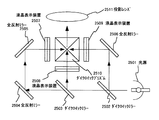
【0196】
図17において、2501は白色光源、2502ならびに2503はダイクロイックミラー、2504〜2506は全反射ミラー、2507〜2509は本発明の液晶表示装置、および2510はダイクロイックプリズム、および2511は投影レンズである。
【0197】
(実施例10)
【0198】
また、上述の本発明の液晶表示装置は、図18に示すような単板式のプロジェクタに用いることもできる。
【0199】
図18において、2601はランプとリフレクターとから成る白色光源である。2602、2603、および2604は、ダイクロイックミラーであり、それぞれ青、赤、緑の波長領域の光を選択的に反射する。2605はマイクロレンズアレイであり、複数のマイクロレンズによって構成されている。2606は本発明の液晶表示装置である。2607は集光レンズ、2608は投射レンズ、2609はスクリーンである。
【0200】
(実施例11)
【0201】
上記実施例8〜10のプロジェクターは、その投影方法によってリアプロジェクターとフロントプロジェクターとがある。
【0202】
図19(A)はフロント型プロジェクタ−であり、本体10001、本発明の液晶表示装置10002、光源10003、光学系10004、スクリーン10005で構成されている。なお、図19(A)には、液晶表示装置を1つ組み込んだフロントプロジェクターが示されているが、液晶表示装置を3個(R、G、Bの光にそれぞれ対応させる)組み込んことによって、より高解像度・高精細のフロント型プロジェクタを実現することができる。
【0203】
図19(B)はリア型プロジェクターであり、10006は本体、10007は液晶表示装置であり、10008は光源であり、10009はリフレクター、10010はスクリーンである。なお、図19(B)には、アクティブマトリクス型半導体表示装置を3個(R、G、Bの光にそれぞれ対応させる)組み込んだリア型プロジェクタが示されている。
【0204】
(実施例12)
【0205】
本実施例では、本発明の液晶表示装置をゴーグル型ディスプレイに用いた例を示す。
【0206】
図20を参照する。2801はゴーグル型ディスプレイ本体である。2802−Rならびに2802−Lは本発明の液晶表示装置であり、2803−Rならびに2803−LはLEDバックライトであり、2804−Rならびに2804−Lは光学素子である。
【0207】
(実施例13)
本発明の液晶表示装置を表示媒体として組み込んだ電子機器を例に挙げる。
【0208】
その様な電子機器としては、ビデオカメラ、デジタルカメラ、プロジェクター(リア型またはフロント型)、ヘッドマウントディスプレイ(ゴーグル型ディスプレイ)、カーナビゲーション、パーソナルコンピュータ、携帯情報端末(モバイルコンピュータ、携帯電話または電子書籍等)などが挙げられる。それらの一例を図21に示す。
【0209】
図21(A)はパーソナルコンピュータであり、本体11001、画像入力部11002、本発明の液晶表示装置11003、キーボード11004で構成される。
【0210】
図21(B)はビデオカメラであり、本体12001、本発明の液晶表示装置12002、音声入力部12003、操作スイッチ12004、バッテリー12005、受像部12006で構成される。
【0211】
図21(C)はモバイルコンピュータ(モービルコンピュータ)であり、本体13001、カメラ部13002、受像部13003、操作スイッチ13004、本発明の液晶表示装置13005で構成される。
【0212】
図21(D)はデジタルカメラであり、本体14001、本発明の液晶表示装置14002、接眼部14003、操作スイッチ14004、受像部(図示しない)で構成される。
【0213】
図21(E)は携帯書籍(電子書籍)であり、本体15001、本発明の液晶表示装置15002、15003、記憶媒体15004、操作スイッチ15005、アンテナ15006で構成される。
【0214】
図21(F)は映像やプログラムを記録した記録媒体(以下、記録媒体と呼ぶ)を用いるプレーヤーであり、本体16001、液晶表示装置16002、スピーカ部16003、記録媒体16004、操作スイッチ16005で構成される。なお、この装置は記録媒体としてDVD(Digtal VersatileDisc)、CD等を用い、音楽鑑賞や映画鑑賞やゲームやインターネットを行うことができる。
【0215】
以上の様に、本発明の液晶表示装置の適用範囲は極めて広く、あらゆる分野の電子機器に適用することが可能である。
【0216】
【発明の効果】
【0217】
本発明の液晶表示装置によると、1つのフレームを構成する複数のサブフレームのうち少なくとも1個のサブフレームにはリセット信号が供給され黒の表示が行われるので、画面の焼付きを防ぐことができる。
【0218】
また、本発明の液晶表示装置においては、連続するサブフレームに絶対値が等しく反対極性の画像信号が同じ画素TFTに供給されるので、画像信号が液晶分子に供給された時に蓄積される液晶分子の自発分極と反対極性の電荷がキャンセルされる。かつ、すくなくとも1つのサブフレームには、ほぼ黒の画像表示が行われる。よって、表示の「焼付き」を防止することができ、良好な表示を実現することができる。
【図面の簡単な説明】
【図1】 無しきい値反強誘電性混合液晶の電気光学特性を示すグラフである。
【図2】 本発明の液晶表示装置の駆動タイミングチャートである。
【図3】 本発明の液晶表示装置の駆動タイミングチャートである。
【図4】 本発明の液晶表示装置のある実施例の概略構成図である。
【図5】 本発明の液晶表示装置のある実施例の画素部、ソースドライバおよびゲートドライバの回路構成図である。
【図6】 本発明の液晶表示装置のある実施例の画素部、ソースドライバおよびゲートドライバの回路構成図である。
【図7】 本発明の液晶表示装置のある実施例のD/A変換回路の回路構成図である。
【図8】 本発明の液晶表示装置の駆動タイミングチャートである。
【図9】 本発明の液晶表示装置の駆動タイミングチャートである。
【図10】 本発明の液晶表示装置のある実施例の概略構成図である。
【図11】 本発明の液晶表示装置の作製工程例を示す図である。
【図12】 本発明の液晶表示装置の作製工程例を示す図である。
【図13】 本発明の液晶表示装置の作製工程例を示す図である。
【図14】 本発明の液晶表示装置の作製工程例を示す図である。
【図15】 本発明の液晶表示装置の作製工程例を示す図である。
【図16】 本発明の液晶表示装置を用いた3板式プロジェクタの概略構成図である。
【図17】 本発明の液晶表示装置を用いた3板式プロジェクタの概略構成図である。
【図18】 本発明の液晶表示装置を用いた単板式プロジェクタの概略構成図である。
【図19】 本発明の液晶表示装置を用いたフロントプロジェクタおよびリアプロジェクタの概略構成図である。
【図20】 本発明の液晶表示装置を用いたゴーグル型ディスプレイの概略構成図である。
【図21】 本発明の液晶表示装置を用いた電子機器の例である。
【図22】 本発明の液晶表示装置の駆動タイミングチャートである。
【図23】 本発明の液晶表示装置のある実施例の概略構成図である。
【図24】 本発明の液晶表示装置のある実施例の画素部、ソースドライバおよびゲートドライバの回路構成図である。
【図25】 本発明の液晶表示装置のある実施例の画素部、ソースドライバおよびゲートドライバの回路構成図である。
【図26】 本発明の液晶表示装置の駆動タイミングチャートである。
【図27】 本発明の液晶表示装置の駆動タイミングチャートである。
【図28】 本発明の液晶表示装置のある実施例の概略構成図である。
【符号の説明】
101 液晶表示装置
101−1 アクティブマトリクス基板
101−2 対向基板
101−1−1 ソースドライバ
101−1−2 ゲートドライバ
101−1−3 ゲートドライバ
101−1−4 画素部
101−1−3 デジタルビデオデータ分割回路
103−1 FPC
103−2 FPC[0001]
BACKGROUND OF THE INVENTION
[0002]
The present invention relates to a liquid crystal display device. The present invention also relates to an electro-optical device using a liquid crystal display device.
[0003]
[Prior art]
[0004]
Recently, a technique for manufacturing a thin film transistor (TFT) on an inexpensive glass substrate has been rapidly developed. The reason is that the demand for active matrix liquid crystal display devices has increased.
[0005]
In an active matrix liquid crystal display device, a pixel portion is configured by several tens to several millions of pixels arranged in a matrix, and a pixel TFT is disposed in each pixel. A pixel electrode connected to each pixel TFT is connected to a pixel electrode. The incoming and outgoing charges are controlled by the switching function of the pixel TFT.
[0006]
In recent years, an active matrix liquid crystal display device has become widespread as a display of a desktop personal computer as well as a display of a notebook personal computer that has been often used.
[0007]
Personal computers are required to display multiple pieces of information (including character information and image information) at the same time, improving the display capabilities of personal computers, that is, increasing the resolution of images and displaying multiple gradations. (Preferably full color display) has been attempted.
[0008]
With the improvement of the display capability of such a personal computer, improvement of an active matrix liquid crystal display device as the display device is being promoted. Therefore, recently, an active matrix liquid crystal display device of a digital drive system that can easily interface with a personal computer, can drive a driver at a high speed, and can realize an improvement in display capability has attracted attention.
[0009]
[Problems to be solved by the invention]
[0010]
Digital video data is input from a data source such as a personal computer to a digital drive type active matrix liquid crystal display device. An active matrix liquid crystal display device having a digital driver has a D / A conversion circuit (also referred to as a DAC: Digital-Analog Converter) that converts digital video data input from the outside into analog data (gradation voltage). is necessary. There are various types of D / A conversion circuits.
[0011]
One of the characteristics of an active matrix liquid crystal display device having a digital driver is that so-called line-sequential driving, in which pixels for one line can be driven simultaneously, can be realized relatively easily.
[0012]
In addition, when the active matrix type liquid crystal display device has a large screen and high definition, the response speed is not sufficient in the conventional TN mode (twisted nematic mode) using nematic liquid crystal.
[0013]
Therefore, recently, an active matrix liquid crystal display device using an antiferroelectric mixed liquid crystal having a V-shaped electro-optic characteristic having a response speed two to three orders of magnitude faster than that of a nematic liquid crystal has been reported.
[0014]
However, when this anti-ferroelectric mixed liquid crystal having V-shaped electro-optical characteristics is used in an active matrix liquid crystal display device, image “burn-in” is more likely to occur than when nematic liquid crystal is used. Deterioration is a problem.
[0015]
Accordingly, the present invention has been made in view of the above-described problems, and realizes a liquid crystal display device that can prevent image deterioration due to image sticking.
[0016]
[Means for Solving the Problems]
[0017]
According to the present invention,
A pixel portion in which a plurality of pixel TFTs are arranged in a matrix;
A source driver and a gate driver for supplying an image signal to the plurality of pixel TFTs;
A ferroelectric liquid crystal material having substantially no threshold;
A liquid crystal display device comprising:
One frame is formed by a plurality of subframes,
A liquid crystal display device is provided in which display is performed in at least one subframe of the plurality of subframes by a reset signal.
[0018]
Moreover, according to the present invention,
A pixel portion in which a plurality of pixel TFTs are arranged in a matrix;
A source driver and a gate driver for supplying an image signal to the plurality of pixel TFTs;
A ferroelectric liquid crystal material having substantially no threshold;
A liquid crystal display device comprising:
One frame is formed by a plurality of subframes,
A liquid crystal display device is provided in which black is displayed by a reset signal in at least one subframe of the plurality of subframes.
[0019]
Moreover, according to the present invention,
A pixel portion in which a plurality of pixel TFTs are arranged in a matrix;
A source driver and a gate driver for supplying an image signal to the plurality of pixel TFTs;
A ferroelectric liquid crystal material having substantially no threshold;
A liquid crystal display device comprising:
One frame is formed by n subframes (n is a natural number of 2 or more),
A liquid crystal display device is provided in which display is performed in m subframes (1 ≦ m <n, where m is a natural number) among the n subframes.
[0020]
Moreover, according to the present invention,
A pixel portion in which a plurality of pixel TFTs are arranged in a matrix;
A source driver and a gate driver for supplying an image signal to the plurality of pixel TFTs;
A ferroelectric liquid crystal material having substantially no threshold;
A liquid crystal display device comprising:
One frame is formed by n subframes (n is a natural number of 2 or more),
A liquid crystal display device, wherein black is displayed by a reset signal in m subframes (1 ≦ m <n, where m is a natural number) of the n subframes.
[0021]
According to the present invention,
A pixel portion in which a plurality of pixel TFTs are arranged in a matrix;
A source driver and a gate driver for supplying an image signal to the plurality of pixel TFTs;
A ferroelectric liquid crystal material having substantially no threshold;
A liquid crystal display device comprising:
A display of one frame is formed by the display of a plurality of subframes,
The display of the plurality of sub-frames is formed by applying image signals having the same absolute value and opposite polarities to the same pixel TFT,
A liquid crystal display device is provided in which a black image is displayed by a reset signal in at least one subframe of the plurality of subframes.
[0022]
Moreover, according to the present invention,
A pixel portion in which a plurality of pixel TFTs are arranged in a matrix;
A source driver and a gate driver for supplying an image signal to the plurality of pixel TFTs;
A ferroelectric liquid crystal material having substantially no threshold;
A liquid crystal display device comprising:
A display of 1 frame is formed by display of m subframes (m is a natural number),
At least n subframes among the m subframes are displayed with a black image by a reset signal (n is a natural number, m> n),
A display of (mn) subframes is formed by applying image signals having the same absolute value and opposite polarities to the same pixel TFT as a pair. Is done.
[0023]
Hereinafter, the liquid crystal display device of the present invention will be described in more detail with reference to examples.
However, the liquid crystal display device of the present invention is not limited to the following examples.
[0024]
DETAILED DESCRIPTION OF THE INVENTION
[0025]
The liquid crystal display device of the present invention uses a ferroelectric liquid crystal material, particularly an antiferroelectric mixed liquid crystal having electro-optical characteristics as shown in FIG.
[0026]
A liquid crystal exhibiting an antiferroelectric phase in a certain temperature range is called an antiferroelectric liquid crystal. Among mixed liquid crystals having antiferroelectric liquid crystals, there is a so-called thresholdless antiferroelectric mixed liquid crystal that exhibits electro-optic response characteristics in which transmittance continuously changes with respect to an electric field. This thresholdless antiferroelectric mixed liquid crystal has a V-shaped electro-optic response characteristic, and a drive voltage of about ± 2.5 V (cell thickness of about 1 μm to 2 μm) is also found. ing.
[0027]
FIG. 1 shows an example of characteristics of light transmittance with respect to an applied voltage of a thresholdless antiferroelectric mixed liquid crystal exhibiting a V-shaped electro-optic response. The vertical axis of the graph shown in FIG. 1 is the transmittance (arbitrary unit), and the horizontal axis is the applied voltage. The transmission axis of the polarizing plate on the incident side of the liquid crystal display device is set to be substantially parallel to the normal direction of the smectic layer of the thresholdless antiferroelectric mixed liquid crystal that substantially coincides with the rubbing direction of the liquid crystal display device. . Further, the transmission axis of the output-side polarizing plate is set to be substantially perpendicular (crossed Nicols) to the transmission axis of the incident-side polarizing plate.
[0028]
When a thresholdless antiferroelectric mixed liquid crystal as shown in FIG. 1 is used, high speed driving, low voltage driving and gradation display are possible.
[0029]
In the liquid crystal display device of the present invention, one screen is displayed by displaying a plurality of subframes at high speed. A reset signal is applied to at least one subframe of the plurality of subframe displays. The reset signal may display black on the screen.
[0030]
Please refer to FIG. FIG. 2 shows a drive timing chart of the liquid crystal display device of the present invention. In describing the present invention, the terms frame and subframe are used. One screen display is called one frame, and one frame is formed by a plurality of subframes. In addition, a time required to display one frame is called one frame period (Tf), and a period obtained by dividing the one frame period (Tf) into a plurality is called a subframe period (Tsf).
[0031]
In the liquid crystal display device of the present invention described here, one frame is formed by two subframes. Here, one frame period (Tf) is composed of a first subframe period (1st Tsf) and a second subframe period (2nd Tsf).
[0032]
First, display of the first frame period will be described. In the first subframe period (1st Tsf), the image signal D is transmitted to the corresponding pixel TFT.1Is supplied and an image is displayed. Next, in the second sub-frame period (2nd Tsf), the reset signal R is supplied to the corresponding pixel TFT, and black display is performed.
[0033]
In the display of the next frame period, similarly to the display of the first frame period, the image signal D is transmitted to the corresponding pixel TFT in the first subframe period (1st Tsf).2Is supplied and an image is displayed. Next, in the second sub-frame period (2nd Tsf), the reset signal R is supplied to the corresponding pixel TFT, and black display is performed.
[0034]
Similarly, continuous frames are displayed and an image is formed.
[0035]
As described above, in the above-described liquid crystal display device of the present invention, one of the two subframes constituting one frame is displayed in black, thereby preventing screen burn-in. it can.
[0036]
Reference is now made to FIG. FIG. 3 shows another driving timing chart of the liquid crystal display device of the present invention.
[0037]
In the liquid crystal display device of the present invention described here, one frame is formed by four subframes. Here, one frame period (Tf) is a first subframe period (1st Tsf), a second subframe period (2nd Tsf), a third subframe period (3rd Tsf), and a fourth subframe period ( 4th Tsf).
[0038]
First, display of the first frame period will be described. In the first subframe period (1st Tsf), the image signal D is transmitted to the corresponding pixel TFT.1Is supplied and an image is displayed. Next, in the second sub-frame period (2nd Tsf), the reset signal R is supplied to the corresponding pixel TFT, and black display is performed. Next, in the third sub-frame period (3rd Tsf), the same image signal D as the signal supplied to the corresponding pixel TFT in the first sub-frame period.1Is supplied and an image is displayed. Next, in the fourth subframe period (4th Tsf), the reset signal R is supplied to the corresponding pixel TFT, and black display is performed.
[0039]
Thus, in the liquid crystal display device of the present invention, when an image signal other than the reset signal is supplied to each subframe in the same frame period, the same image signal is supplied.
[0040]
In the display of the next frame period, similarly to the display of the first frame period, the image signal D is transmitted to the corresponding pixel TFT in the first subframe period (1st Tsf).2Is supplied and an image is displayed. Next, in the second sub-frame period (2nd Tsf), the reset signal R is supplied to the corresponding pixel TFT, and black display is performed. Next, in the third sub-frame period (3rd Tsf), the same image signal D as the signal supplied to the corresponding pixel TFT in the first sub-frame period.2Is supplied and an image is displayed. Next, in the fourth subframe period (4th Tsf), the reset signal R is supplied to the corresponding pixel TFT, and black display is performed.
[0041]
Similarly, continuous frames are displayed and an image is formed.
[0042]
As described above, in the liquid crystal display device of the present invention, a black signal is displayed by supplying a reset signal to at least one subframe among a plurality of subframes constituting one frame. Can be prevented.
[0043]
In the above example, when one frame is formed by two subframes, and when one frame is formed by four subframes, and when supply of an image signal and supply of a reset signal are alternately performed. However, the present invention is not limited to these cases. In the liquid crystal display device of the present invention, one frame can be composed of n subframes (1 ≦ m <n, where m is a natural number), and supply of an image signal and supply of a reset signal are arbitrarily set. May be.
[0044]
Hereinafter, the liquid crystal display device of the present invention will be described in more detail with reference to examples. However, the liquid crystal display device of the present invention is not limited to the following examples.
[0045]
【Example】
[0046]
(Example 1)
[0047]
Please refer to FIG. FIG. 4 shows a schematic configuration diagram of the liquid crystal display device of the present embodiment. Reference numeral 101 denotes a liquid crystal display device having a digital driver. The liquid crystal display device 101 includes an active matrix substrate 101-1 and a counter substrate 101-2 (not shown). The active matrix substrate 101-1 includes a source driver 101-1-1, a gate driver 101-1-2, a digital video data division circuit 101-1-3, and a pixel unit 101-in which a plurality of pixel TFTs are arranged in a matrix. 1-4. The source driver 101-1-1 and the gate driver 101-1-2 drive a plurality of pixel TFTs in the pixel portion. The counter substrate 101-2 has a counter electrode 101-2-1 (not shown). Reference numerals 103-1 and 103-2 denote FPC (Flexible Print Circuit) terminals, and various signals are inputted to these FPC terminals from the outside.
[0048]
Reference is now made to FIG. FIG. 5 is a schematic configuration diagram showing in detail the source driver of the liquid crystal display device of this embodiment. 101-1-1 is a source driver. 101-1-2 is a gate driver. Reference numeral 101-1-4 denotes a pixel portion. Reference numeral 101-1-3 denotes a digital video data division circuit (SPC; Serial-to-Parallel Conversion Circuit).
[0049]
The source driver 101-1-1 includes a shift register circuit (240 stage × 2 shift register circuit) 501, a latch circuit 1 (960 × 8 digital latch circuit) 502, a latch circuit 2 (960 × 8 digital latch circuit) 503, A selector circuit 1 (a selector circuit of 240) 504, a D / A conversion circuit (a DAC of 240) 505, and a selector circuit 2 (a selector circuit of 240) 506 are provided. In addition, a buffer circuit and a level shifter circuit (both not shown) are included. For convenience of explanation, the D / A conversion circuit 505 includes a level shifter circuit.
[0050]
Reference numeral 101-1-2 denotes a gate driver, which includes a shift register circuit, a buffer circuit, a level shifter circuit, and the like (all not shown).
[0051]
The pixel unit 101-1-4 has 1920 × 1080 (horizontal × vertical) pixels. A pixel TFT is disposed in each pixel. A source signal line is electrically connected to the source region of each pixel TFT, and a gate signal line is electrically connected to the gate electrode. A pixel electrode is electrically connected to the drain region of each pixel TFT. Each pixel TFT controls the supply of an image signal (gradation voltage) to a pixel electrode electrically connected to each pixel TFT. An image signal (gradation voltage) is supplied to each pixel electrode, and a voltage is applied to the liquid crystal sandwiched between each pixel electrode and the counter electrode to drive the liquid crystal.
[0052]
Here, the operation and signal flow of the active matrix liquid crystal display device of this embodiment will be described.
[0053]
First, the operation of the source driver will be described. A clock signal (CK) and a start pulse (SP) are input to the shift register circuit 501. The shift register circuit 501 sequentially generates timing signals based on the clock signal (CK) and the start pulse (SP), and sequentially supplies the timing signals to subsequent circuits through a buffer circuit or the like (not shown).
[0054]
A timing signal from the shift register circuit 501 is buffered by a buffer circuit or the like. Since many circuits or elements are connected to the source signal line to which the timing signal is supplied, the load capacitance (parasitic capacitance) is large. This buffer circuit is provided in order to prevent “dullness” of the rise of the timing signal caused by the large load capacity.
[0055]
The timing signal buffered by the buffer circuit is supplied to the latch circuit 1 (502). The latch circuit 1 (502) has 960 stages of latch circuits for processing 8-bit digital video data. When the timing signal is input, the latch circuit 1 (502) sequentially captures and holds 8-bit digital video data supplied from the digital video data dividing circuit 101-1-3.
[0056]
The time until digital video data is completely written to the latch circuit in all the stages of the latch circuit 1 (502) is called a line period. That is, from the time when writing of digital video data to the latch circuit of the leftmost stage in the latch circuit 1 (502) is started, the time of writing of digital video data to the latch circuit of the rightmost stage is completed. The time interval until is the line period. Actually, a period obtained by adding a horizontal blanking period to the line period may be called a line period.
[0057]
After the end of one line period, a latch signal (Latch Signal) is supplied to the latch circuit 2 (503) in accordance with the operation timing of the shift register circuit 501. At this moment, the digital video data written and held in the latch circuit 1 (502) is sent all at once to the latch circuit 2 (503) and written and held in the latch circuits of all stages of the latch circuit 2 (503). Is done.
[0058]
The digital video data supplied from the digital video data dividing circuit is written again to the latch circuit 1 (502) which has finished sending the digital video data to the latch circuit 2 (503) based on the timing signal from the shift register circuit 501. Are performed sequentially.
[0059]
During the second line period, the digital video data written and held in the latch circuit 2 (503) is sequentially selected by the selector circuit 1 (504) and supplied to the D / A conversion circuit 505. Is done. In this embodiment, in the selector circuit 1 (504), one selector circuit corresponds to four source signal lines.
[0060]
As the selector circuit, the one described in Japanese Patent Application No. 9-286098, which is a patent application by the present applicant, can be used.
[0061]
The 8-bit digital video data from the latch circuit 2 (503) selected by the selector circuit 504 is supplied to the D / A conversion circuit 505. Here, the D / A conversion circuit used in this embodiment will be described with reference to FIG.
[0062]
FIG. 7 shows a circuit diagram of the D / A conversion circuit of this embodiment. Note that the D / A conversion circuit of this embodiment includes a level shifter circuit (LS) 505-2, but the level shifter circuit may be omitted and designed. In the level shifter circuit, when the signal Lo is input to the input IN and the signal Hi is input to the input INb, the high potential power supply VddHI is output from the output OUT, and the low potential power supply Vss is output from the output OUTb. ing. Further, when the signal Hi is input to the input IN and the signal Lo is input to the input INb, the high potential power supply Vss is output from the output OUT, and the low potential power supply VddHI is output from the output OUTb.
[0063]
In the D / A conversion circuit of this embodiment, inverted data of digital video data A0 to A7 (herein referred to as inverted A0 to inverted A7) is input to one input of the NOR circuit (505-1). It has become. The reset pulse A (ResA) is input to the other input of the NOR circuit (505-1). The reset pulse A is input during the reset period TR of the D / A conversion circuit. In this embodiment, the digital video data (inverted A0 to A7) is input to the NOR circuit (505-1) even during the reset period TR. However, while the reset pulse ResA is input to the NOR circuit, NOR is performed. Digital video data is not output from the circuit.
[0064]
Note that the NOR circuit may be omitted, and digital video data (inverted A0 to A7) may be input after the reset period TR ends.
[0065]
After the reset period TR ends, the data writing period TE starts, and the 8-bit digital video data is raised in voltage by the level shifter circuit and input to the switch circuits SW0 to SW7.
[0066]
Each of the switch circuits SW0 to SW7 is composed of two analog switches ASW1 and ASW2. One end of ASW1 is connected to DC_VIDEO_L, and the other end is connected to one end of ASW2 and connected to a capacitor. One end of each ASW2 is connected to DC_VIDEO_H, and the other end is connected to one end of ASW1 and connected to a capacitor (1pF, 2pF, 4pF, 8pF, 1pF, 2pF, 4pF, 8pF). One end of each capacitor is connected to two analog switches, and the other end is connected to a reset switch 2 (Res2). One end of the reset switch 1 (Res1) is connected to DC_VIDEO_M, and the other end is connected to one end of a capacitor corresponding to the upper bit. A reset pulse (ResB) and an inverted reset pulse (inverted ResB) are input to the reset switches Res1 and Res2.
[0067]
Further, a capacitor (1 pF) is provided at a connection point between the circuit corresponding to the upper bit and the circuit corresponding to the lower bit. In the present embodiment, all the above-mentioned capacities are not limited to those values.
[0068]
The D / A conversion circuit 505 converts 8-bit digital video data into an image signal (gradation voltage), and sequentially supplies it to the source signal line selected by the selector circuit 2 (506).
[0069]
The image signal supplied to the source signal line is supplied to the source region of the pixel TFT of the pixel portion connected to the source signal line.
[0070]
In the gate driver 101-1-2, a timing signal (scanning signal) from a shift register (not shown) is supplied to a buffer circuit (not shown) and supplied to a corresponding gate signal line (scanning line). . A gate electrode of a pixel TFT for one line is connected to the gate signal line, and all the pixel TFTs for one line must be turned on at the same time. Therefore, a buffer circuit having a large current capacity is used. .
[0071]
In this manner, the corresponding pixel TFT is switched by the scanning signal from the gate driver, the image signal (gradation voltage) from the source driver is supplied to the pixel TFT, and the liquid crystal molecules are driven.
[0072]
Reference numeral 101-1-3 denotes a digital video data division circuit (SPC; Serial-to-Parallel Conversion Circuit). The digital video data dividing circuit 101-1-3 is a circuit for reducing the frequency of digital video data input from the outside to 1 / x (x is a natural number of 2 or more). By dividing the digital video data input from the outside, the frequency of the signal necessary for the operation of the driving circuit can be reduced to 1 / x.
[0073]
Here, the circuit configuration of the liquid crystal display device 101 of this embodiment, particularly the configuration of the pixel portion 101-1-4, will be described with reference to FIG.
[0074]
In the present embodiment, the pixel unit 101-1-4 has (1920 × 1080) pixels. For convenience of explanation, reference numerals such as P1,1, P2,1,..., P1079, 1919 are attached to the respective pixels. Each pixel has a
[0075]
The liquid crystal display device of this embodiment performs so-called line-sequential driving that simultaneously drives pixels for one line (for example, P1,1, P1,2,..., And P1,1919). In other words, the image progression is simultaneously written in all the pixels for one line.
[0076]
Here, a display method of the liquid crystal display device of this embodiment will be described. Please refer to FIG. FIG. 8 shows a drive timing chart of the liquid crystal display device of this embodiment. In the liquid crystal display device of the present invention described here, one frame is formed by two subframes. Here, one frame period (Tf) is composed of a first subframe period (1st Tsf) and a second subframe period (2nd Tsf).
[0077]
In FIG. 8, a pixel P1,1, a pixel P2,1, and a pixel P1079,1 are shown as an example.
[0078]
First, display of the first frame period will be described. A scanning signal is input to the gate driver in the first subframe period (1st Tsf), and digital video data is D / A converted into the pixels P1,1 to P1,1919 in the first subframe line period (1st Tsfl). It is converted into an image signal and written by a circuit. Thereafter, in the next subframe line period, digital video data is converted into an image signal by the D / A conversion circuit and written to the pixels P2,1 to P2,1919. Thereafter, the image signal is written in order to each pixel, the image signal is written to the last one line of pixels P1079,1 to P1079,1919, and the first subframe period ends.
[0079]
Next, the second subframe period (2nd Tsf) starts. A scanning signal is input to the gate driver in the second subframe period (2nd Tsf), and digital video data is D / A converted into pixels P1,1 to P1,1919 in the second subframe line period (2nd Tsfl). The reset signal converted by the circuit is written and black display is performed. Thereafter, in the next subframe line period, a reset signal obtained by converting the digital video data by the D / A conversion circuit is written to the pixels P2,1 to P2,1919, and black display is performed. Thereafter, a reset signal is sequentially written in each pixel, and the reset signal is written in the last one line of pixels P1079,1 to P1079,1919, and black display is performed. Thus, the second subframe period ends.
[0080]
In the display of the next frame period, similarly to the display of the first frame period, the image signal D is transmitted to the corresponding pixel TFT in the first subframe period (1st Tsf).2Is supplied and an image is displayed. Next, in the second sub-frame period (2nd Tsf), the reset signal R is supplied to the corresponding pixel TFT, and black display is performed.
[0081]
Similarly, continuous frames are displayed and an image is formed.
[0082]
As described above, in the above-described liquid crystal display device of the present invention, one of the two subframes constituting one frame is displayed in black, thereby preventing screen burn-in. it can.
[0083]
(Example 2)
[0084]
In this embodiment, a liquid crystal display device of the present invention by a display method different from that of the first embodiment will be described. In addition, since the structure of the liquid crystal display device of a present Example is the same as that of Example 1, Example 1 can be referred.
[0085]
A display method of the liquid crystal display device of this embodiment will be described. Please refer to FIG. FIG. 9 shows a drive timing chart of the liquid crystal display device of this embodiment. In the liquid crystal display device of the present invention described here, one frame is formed by four subframes. Here, one frame period (Tf) is a first subframe period (1st Tsf), a second subframe period (2nd Tsf), a third subframe period (3rd Tsf), and a fourth subframe period ( 4th Tsf).
[0086]
In FIG. 9, pixel P1,1, pixel P2,1, and pixel P1079,1 are shown as an example.
[0087]
First, display of the first frame period will be described. A scanning signal is input to the gate driver in the first subframe period (1st Tsf), and digital video data is D / A converted into the pixels P1,1 to P1,1919 in the first subframe line period (1st Tsfl). It is converted into an image signal and written by a circuit. The pixel P1,1 shown in FIG.1Is written. Thereafter, in the next subframe line period, digital video data is converted into an image signal by the D / A conversion circuit and written to the pixels P2,1 to P2,1919. The pixel P2,1 shown in FIG.ThreeIs written. Thereafter, the image signal is written in order to each pixel, and the image signal is written in the last one line of pixels P1079,1 to P1079,1919. The pixel P1079,1 shown in FIG.FiveIs written. Thus, the first subframe period ends.
[0088]
Next, the second subframe period (2nd Tsf) starts. A scanning signal is input to the gate driver in the second subframe period (2nd Tsf), and digital video data is D / A converted into pixels P1,1 to P1,1919 in the second subframe line period (2nd Tsfl). The reset signal converted by the circuit is written and black display is performed. Thereafter, in the next subframe line period, a reset signal obtained by converting the digital video data by the D / A conversion circuit is written to the pixels P2,1 to P2,1919, and black display is performed. Thereafter, a reset signal is sequentially written in each pixel, and the reset signal is written in the last one line of pixels P1079,1 to P1079,1919, and black display is performed. Thus, the second subframe period ends.
[0089]
Next, the third subframe period (3rd Tsf) starts. In the third subframe period (3rd Tsf), the scanning signal is input to the gate driver, and in the third subframe line period (3rd Tsfl), the digital video data is D / A converted into the pixels P1,1 to P1,1919. It is converted into an image signal and written by a circuit. The pixel P1,1 shown in FIG. 9 has the same image signal D as that in the first subframe period.1Is written. Thereafter, in the next subframe line period, digital video data is converted into an image signal by the D / A conversion circuit and written to the pixels P2,1 to P2,1919. The pixel P2,1 shown in FIG. 9 has the same image signal D as that in the first subframe period.ThreeIs written. Thereafter, the image signal is written in order to each pixel, and the image signal is written in the last one line of pixels P1079,1 to P1079,1919. The pixel P1079,1 shown in FIG. 9 has the same image signal D as that in the first subframe period.FiveIs written. Thus, the first subframe period ends.
[0090]
Next, the fourth subframe period (4th Tsf) starts. In the fourth subframe period (4th Tsf), the scanning signal is input to the gate driver, and in the fourth subframe line period (4th Tsfl), the digital video data is D / A converted to the pixels P1,1 to P1,1919. The reset signal converted by the circuit is written and black display is performed. Thereafter, in the next subframe line period, a reset signal obtained by converting the digital video data by the D / A conversion circuit is written to the pixels P2,1 to P2,1919, and black display is performed. Thereafter, a reset signal is sequentially written in each pixel, and the reset signal is written in the last one line of pixels P1079,1 to P1079,1919, and black display is performed. Thus, the fourth subframe period ends.
[0091]
Thus, the first frame period ends. Thereafter, the next frame period starts and the first to fourth subframes are displayed.
[0092]
Similarly, continuous frames are displayed and an image is formed.
[0093]
Thus, in the above-described liquid crystal display device of the present invention, black display is performed in two subframes out of four subframes constituting one frame, thereby preventing screen burn-in. be able to.
[0094]
(Example 3)
[0095]
Please refer to FIG. FIG. 10 shows a schematic configuration diagram of the liquid crystal display device of this embodiment. Reference numeral 1001 denotes a liquid crystal display device having a digital driver. The liquid crystal display device 1001 includes an active matrix substrate 1001-1 and a counter substrate 1001-2 (not shown). An active matrix substrate 1001-1 includes a source driver 1001-1-1, a source driver 1001-1-2, a gate driver 1001-1-3, a digital video data division circuit 1001-1-4, and a plurality of pixel TFTs. The pixel portion 1001-1-5 is disposed in the area. The source driver 1001-1-1, the source driver 1001-1-2, and the gate driver 1001-1-3 drive a plurality of pixel TFTs in the pixel portion. The counter substrate 1001-2 has a counter electrode 1001-2-1 (not shown). Reference numerals 1003-1 and 1003-2 denote FPC terminals, and various signals are input to these FPC terminals from the outside.
[0096]
The source driver 1001-1-1 drives pixels connected to odd-numbered source signal lines in the pixel portion, and the source driver 1001-1-2 drives pixels connected to even-numbered source signal lines in the pixel portion. To do.
[0097]
Other configurations are the same as those of the first embodiment.
[0098]
Example 4
[0099]
Refer to FIG. FIG. 22 shows a drive timing chart of the liquid crystal display device of this embodiment. In describing the present invention, the terms frame and subframe are used. One screen display is called one frame, and one frame is formed by a plurality of subframes. Also, the time required to display one frame is called one frame period (Tf), and the period corresponding to the display of a plurality of subframes constituting one frame period (Tf) is called a subframe period (Tsf). .
[0100]
In the liquid crystal display device of the present invention, one screen is displayed by displaying a plurality of subframes at high speed. When displaying a certain frame, the image signal for displaying a certain subframe and the image signal for displaying the next subframe have the same absolute value from the reference potential and have the opposite polarity. . In the liquid crystal display device of the present invention, these two sub-frames are always displayed in pairs.
[0101]
In addition to the above-described operation, a reset signal is applied to at least one subframe of the plurality of subframe displays. In this specification, the reset signal refers to a signal for displaying almost black on the screen.
[0102]
In the liquid crystal display device of the present invention described below, one frame is formed by three subframes. Here, one frame period (Tf) is composed of a first subframe period (1st Tsf), a second subframe period (2nd Tsf), and a third subframe period (3rd Tsf).
[0103]
First, display of the first frame period will be described. In the first sub-frame period (1st Tsf), the image signal (D1) Is supplied, and the liquid crystal molecules are driven to display an image. Next, in the second sub-frame period (2nd Tsf), an image signal (D1) And an opposite polarity image signal (inverted D)1) Is supplied and an image is displayed. Next, in the third subframe period, a reset signal (R) is supplied to the corresponding pixel TFT, and black image display is performed. This reset signal may supply a potential that is the reference potential of the image signal. Moreover, even if it is electric potentials other than a reference electric potential, it should just be a signal which displays a black image.
[0104]
With the above operation, the display of the first frame period ends and the next frame period starts. The display of the next frame period is performed in the same manner as the display of the first frame period. In the first sub-frame period (1st Tsf), the image signal (D2) Is supplied and an image is displayed. Next, in the second sub-frame period (2nd Tsf), an image signal (D2) And an opposite polarity image signal (inverted D)2) Is supplied and an image is displayed. Next, in the third subframe period, a reset signal (R) is supplied to the corresponding pixel TFT, and black image display is performed.
[0105]
Similarly, continuous frames are displayed and an image is formed.
[0106]
As described above, in the liquid crystal display device of the present invention, image signals having the same absolute value and the opposite polarity are supplied to the same pixel TFT in successive subframes, and therefore are stored when the image signal is supplied to the liquid crystal molecules. The charge having the opposite polarity to the spontaneous polarization of the liquid crystal molecules is canceled. In addition, an almost black image is displayed in at least one subframe. Therefore, display “burn-in” can be prevented.
[0107]
In the above example, the case where one frame is formed by three sub-frames has been described, but the present invention is not limited to these cases. In the liquid crystal display device of the present invention, one frame may be formed by m subframes, and a reset signal may be supplied to at least n subframes (m> n, m and n are natural numbers).
[0108]
Refer to FIG. FIG. 23 shows a schematic configuration diagram of the liquid crystal display device of the present embodiment. Reference numeral 7101 denotes a liquid crystal display device having a digital driver. The liquid crystal display device 7101 includes an active matrix substrate 7101-1 and a counter substrate 7101-2 (not shown). The active matrix substrate 7101-1 includes a source driver 7101-1-1, a gate driver 7101-1-2, and a pixel portion 7101-1-3 in which a plurality of pixel TFTs are arranged in a matrix. The source driver 7101-1-1 and the gate driver 7101-1-2 drive a plurality of pixel TFTs in the pixel portion. The counter substrate 7101-2 has a counter electrode 7101-2-1 (not shown). Reference numerals 7103-1 and 7103-2 denote FPC (Flexible Print Circuit) terminals, and various signals are input to these FPC terminals from the outside. Note that 8-bit digital data is input to the liquid crystal display device of this embodiment from the outside.
[0109]
Reference is now made to FIG. FIG. 24 is a schematic configuration diagram showing in detail the source driver of the liquid crystal display device of this embodiment. Reference numeral 7101-1-1 denotes a source driver. Reference numeral 7101-1-2 denotes a gate driver. Reference numeral 7101-1-3 denotes a pixel portion.
[0110]
The source driver 7101-1-1 includes a shift register circuit 7501, a latch circuit 1 (7502), a latch circuit 2 (7503), and a D / A conversion circuit 7504. In addition, a buffer circuit and a level shifter circuit (both not shown) are included. For convenience of explanation, the D / A conversion circuit 7504 includes a level shifter circuit.
[0111]
Reference numeral 7101-1-2 denotes a gate driver, which includes a shift register circuit, a buffer circuit, a level shifter circuit, and the like (all not shown).
[0112]
The pixel portion 7101-1-3 has 1920 × 1080 (horizontal × vertical) pixels. A pixel TFT is disposed in each pixel. A source signal line is electrically connected to the source region of each pixel TFT, and a gate signal line is electrically connected to the gate electrode. A pixel electrode is electrically connected to the drain region of each pixel TFT. Each pixel TFT controls the supply of an image signal (gradation voltage) to a pixel electrode electrically connected to each pixel TFT. An image signal (gradation voltage) is supplied to each pixel electrode, and a voltage is applied to the liquid crystal sandwiched between each pixel electrode and the counter electrode to drive the liquid crystal.
[0113]
Here, the operation and signal flow of the active matrix liquid crystal display device of this embodiment will be described.
[0114]
First, the operation of the source driver will be described. A clock signal (CK) and a start pulse (SP) are input to the shift register circuit 7501. The shift register circuit 7501 sequentially generates timing signals based on the clock signal (CK) and the start pulse (SP), and sequentially supplies the timing signals to subsequent circuits through a buffer circuit or the like (not shown).
[0115]
A timing signal from the shift register circuit 7501 is buffered by a buffer circuit or the like. Since many circuits or elements are connected to the source signal line to which the timing signal is supplied, the load capacitance (parasitic capacitance) is large. This buffer circuit is provided in order to prevent “dullness” of the rise of the timing signal caused by the large load capacity.
[0116]
The timing signal buffered by the buffer circuit is supplied to the latch circuit 1 (7502). When the timing signal is input, the latch circuit 1 (7502) sequentially captures and holds 8-bit digital video data supplied from the outside.
[0117]
The time until digital video data is completely written in the latch circuit in all stages of the latch circuit 1 (7502) is a subframe line period. That is, from the time when writing of digital video data is started to the latch circuit of the leftmost stage in the latch circuit 1 (7502), when writing of digital video data is finished to the latch circuit of the rightmost stage. The time interval until is the subframe line period. Actually, a period obtained by adding a horizontal blanking period to the subframe line period may be called a subframe line period.
[0118]
After the end of one subframe line period, a latch signal (Latch Signal) is supplied to the latch circuit 2 (7503) in accordance with the operation timing of the shift register circuit 7501. At this moment, the digital video data written and held in the latch circuit 1 (7502) is sent all at once to the latch circuit 2 (7503), and written and held in the latch circuits of all stages of the latch circuit 2 (7503). Is done.
[0119]
The digital video data supplied from the outside is sequentially written into the latch circuit 1 (7502) which has finished sending the digital video data to the latch circuit 2 (7503) based on the timing signal from the shift register circuit 7501.
[0120]
During this second subframe line period, the digital video data written and held in the latch circuit 2 (7503) is supplied to the D / A conversion circuit 7504.
[0121]
The D / A conversion circuit 7504 used in the present embodiment may be the same as that shown in FIG. 7 of the first embodiment.
[0122]
Here, a circuit configuration of the liquid crystal display device 7101 of the liquid crystal display device of this embodiment, in particular, a configuration of the pixel portion 7101-1-3 will be described with reference to FIG.
[0123]
In this embodiment, the pixel portion 7101-1-3 has (1920 × 1080) pixels. For convenience of explanation, reference numerals such as P1,1, P2,1,..., P1079, 1919 are attached to the respective pixels. Each pixel has a
[0124]
The liquid crystal display device of this embodiment performs so-called line-sequential driving that simultaneously drives pixels for one line (for example, P1,1, P1,2,..., And P1,1919). In other words, the image signal is simultaneously written in all the pixels for one line.
[0125]
Here, a display method of the liquid crystal display device of this embodiment will be described. Refer to FIG. FIG. 26 shows a drive timing chart of the liquid crystal display device of this embodiment. In the liquid crystal display device of the present invention described here, one frame is formed by three subframes. In this embodiment, one frame period (Tf) includes a first subframe period (1st Tsf), a second subframe period (2nd Tsf), and a third subframe period (3rd Tsf).
[0126]
In FIG. 26, pixel P1,1, pixel P2,1, and pixel P1079,1 are shown as an example.
[0127]
First, display of the first frame period will be described. A start pulse is input to the gate driver in the first subframe period (1st Tsf), and digital video data is D / A converted into the pixels P1,1 to P1,1919 in the first subframe line period (1st Tsfl). It is converted into an image signal and written by a circuit. As shown in FIG. 26, for example, an image signal (D1) Is written.
[0128]
Thereafter, in the next subframe line period, digital video data is converted into an image signal by the D / A conversion circuit and written to the pixels P2,1 to P2,1919. As shown in FIG. 26, for example, an image signal (DFour) Is written.
[0129]
Thereafter, the image signal is written in order to each pixel, the image signal is written to the last one line of pixels P1079,1 to P1079,1919, and the first subframe period ends. As shown in FIG. 26, for example, the pixel P1079,1 has an image signal (D7) Is written.
[0130]
Next, the second subframe period (2nd Tsf) starts. At the start of the second subframe period (2nd Tsf), a start pulse is input to the gate driver, and during the second subframe line period (2nd Tsfl), digital video data is output to the pixels P1,1 to P1,1919 as D / It is converted into an image signal and written by the A conversion circuit. As shown in FIG. 26, for example, the pixel P1,1 has an image signal (inverted D1) Is written.
[0131]
Thereafter, in the next subframe line period, digital video data is converted into an image signal by the D / A conversion circuit and written to the pixels P2,1 to P2,1919. As shown in FIG. 26, for example, the pixel P2,1 has an image signal (inverted DFour) Is written.
[0132]
Thereafter, the image signal is written in order to each pixel, the image signal is written to the last one line of pixels P1079,1 to P1079,1919, and the first subframe period ends. As shown in FIG. 26, for example, the pixel P1079,1 has an image signal (inverted D).7) Is written.
[0133]
Next, the third subframe period (3rd Tsf) starts. A reset signal (R) in which a start pulse is input to the gate driver at the start of the third subframe period (3rd Tsf), and digital video data is converted into pixels P1,1 to P1,1919 by the D / A converter circuit Is written, and a black image is displayed. Thereafter, in the next subframe line period, a reset signal (R) obtained by converting the digital video data by the D / A conversion circuit is written to the pixels P2,1 to P2,1919, and a black image is displayed. . Thereafter, the reset signal (R) is sequentially written to each pixel, and the reset signal (R) is written to the pixels P1079,1 to P1079,1919 for the last one line, thereby displaying a black image. Thus, the third subframe period ends.
[0134]
With the above operation, one frame image display is completed.
[0135]
Similarly, continuous frames are displayed and an image is formed.
[0136]
As described above, in the liquid crystal display device according to the present embodiment, image signals having the same absolute value and opposite polarity are supplied to the same pixel TFT in successive subframes, so that they are stored when the image signal is supplied to the liquid crystal molecules. The charge having the opposite polarity to the spontaneous polarization of the liquid crystal molecules is canceled. In addition, black is displayed in at least one subframe. Therefore, display “burn-in” can be prevented.
[0137]
(Example 5)
[0138]
In this embodiment, a liquid crystal display device of the present invention by a display method different from that of the above-described embodiment 4 will be described. In addition, since the structure of the liquid crystal display device of a present Example is the same as that of Example 4, Example 4 can be referred.
[0139]
Here, a display method of the liquid crystal display device of this embodiment will be described. Refer to FIG. FIG. 27 shows a drive timing chart of the liquid crystal display device of this embodiment. In the liquid crystal display device of the present invention described here, one frame is formed by five subframes. That is, in the present embodiment, one frame period (Tf) is a first subframe period (1st Tsf), a second subframe period (2nd Tsf), a third subframe period (3rd Tsf), and a fourth subframe period. The frame period (4th Tsf) and the fifth subframe period (5th Tsf) are included.
[0140]
In FIG. 27, pixel P1,1, pixel P2,1, and pixel P1079,1 are shown as an example.
[0141]
First, display of the first frame period will be described. A start pulse is input to the gate driver in the first subframe period (1st Tsf), and digital video data is D / A converted into the pixels P1,1 to P1,1919 in the first subframe line period (1st Tsfl). It is converted into an image signal and written by a circuit. As shown in FIG. 27, for example, an image signal (D1) Is written.
[0142]
Thereafter, in the next subframe line period, digital video data is converted into an image signal by the D / A conversion circuit and written to the pixels P2,1 to P2,1919. As shown in FIG. 27, for example, an image signal (DThree) Is written.
[0143]
Thereafter, the image signal is written in order to each pixel, the image signal is written to the last one line of pixels P1079,1 to P1079,1919, and the first subframe period ends. As shown in FIG. 27, for example, the pixel P1079,1 has an image signal (DFive) Is written.
[0144]
Next, the second subframe period (2nd Tsf) starts. At the start of the second subframe period (2nd Tsf), a start pulse is input to the gate driver, and during the second subframe line period (2nd Tsfl), digital video data is output to the pixels P1,1 to P1,1919 as D / It is converted into an image signal and written by the A conversion circuit. As shown in FIG. 27, for example, the pixel P1,1 has an image signal (inverted D1) Is written.
[0145]
Thereafter, in the next subframe line period, digital video data is converted into an image signal by the D / A conversion circuit and written in the pixels P2,1 to P2,1979. As shown in FIG. 27, for example, the pixel P2,1 has an image signal (inverted D).Three) Is written.
[0146]
Thereafter, an image signal is sequentially written to each pixel, the image signal is written to the last one line of pixels P1079,1 to P1079,1919, and the second subframe period ends. As shown in FIG. 27, for example, pixel P1079,1 has an image signal (inverted DFive) Is written.
[0147]
Next, the third subframe period (3rd Tsf) starts. A start pulse is input to the gate driver at the start of the third subframe period (3rd Tsf), and digital video data is output to the pixels P1,1 to P1,1919 in the third subframe line period (3rd Tsfl). It is converted into an image signal and written by the A conversion circuit. As shown in FIG. 27, for example, the same image signal (D as the image signal written in the first subframe line period (1st Tsfl) in the pixel P1,1).1) Is written.
[0148]
Thereafter, in the next subframe line period, digital video data is converted into an image signal by the D / A conversion circuit and written to the pixels P2,1 to P2,1919. As shown in FIG. 27, for example, the same image signal (D as the image signal written in the first subframe line period (1st Tsfl) in the pixel P2,1).Three) Is written.
[0149]
Thereafter, an image signal is sequentially written to each pixel, the image signal is written to the last one line of pixels P1079,1 to P1079,1919, and the third subframe period ends. As shown in FIG. 27, for example, the pixel P1079,1 has the same image signal (D as the image signal written in the first subframe line period (1st Tsfl)).Five) Is written.
[0150]
Next, the fourth subframe period (4th Tsf) starts. At the start of the fourth subframe period (4th Tsf), a start pulse is input to the gate driver, and during the fourth subframe line period (4th Tsfl), digital video data is output to the pixels P1,1 to P1,1919 at D / D It is converted into an image signal and written by the A conversion circuit. As shown in FIG. 27, for example, the pixel P1,1 has the same image signal (inverted D) as the image signal written in the second subframe line period (2nd Tsfl).1) Is written.
[0151]
Thereafter, in the next subframe line period, digital video data is converted into an image signal by the D / A conversion circuit and written to the pixels P2,1 to P2,1919. As shown in FIG. 27, for example, the pixel P2,1 has the same image signal (inverted D) as the image signal written in the second subframe line period (1st Tsfl).Three) Is written.
[0152]
Thereafter, the image signal is written in order to each pixel, the image signal is written to the last one line of pixels P1079,1 to P1079,1919, and the fourth subframe period ends. As shown in FIG. 27, for example, the pixel P1079,1 has the same image signal (inverted D) as the image signal written in the second subframe line period (2nd Tsfl).Five) Is written.
[0153]
Next, the fifth subframe period (5th Tsf) starts. At the start of the fifth subframe period (5th Tsf), a start pulse is input to the gate driver, and in the fifth subframe line period (5th Tsfl), digital video data is input to the pixels P1,1 to P1,1919 at D / D. The reset signal (R) converted by the A conversion circuit is written, and a black image is displayed. Thereafter, in the next subframe line period, a reset signal (R) obtained by converting the digital video data by the D / A conversion circuit is written to the pixels P2,1 to P2,1919, and a black image is displayed. . Thereafter, the reset signal (R) is sequentially written to each pixel, and the reset signal (R) is written to the pixels P1079,1 to P1079,1919 for the last one line, thereby displaying a black image. Thus, the fifth subframe period ends.
[0154]
Thus, the first to fifth subframe periods are finished, and one frame period is finished.
[0155]
Similarly, continuous frames are displayed and an image is formed.
[0156]
As described above, in the liquid crystal display device of this embodiment, one frame display is formed by displaying five subframes at high speed. Therefore, display “burn-in” can be prevented and image flicker can be reduced.
[0157]
(Example 6)
[0158]
Refer to FIG. FIG. 28 shows a schematic configuration diagram of the liquid crystal display device of the present embodiment. Reference numeral 8001 denotes a liquid crystal display device having a digital driver. A liquid crystal display device 8001 includes an active matrix substrate 8001-1 and a counter substrate 8001-2 (not shown). The active matrix substrate 8001-1 includes a source driver 8001-1-1, a source driver 8001-1-2, a gate driver 8001-1-3, a digital video data division circuit 8001-1-4, and a plurality of pixel TFTs in a matrix. The pixel portion 8001-1-5 is disposed in the. The source driver 8001-1-1, source driver 8001-1-2, and gate driver 8001-1-3 drive a plurality of pixel TFTs in the pixel portion. Further, the counter substrate 8001-2 has a counter electrode 8001-2-1 (not shown). 8003-1 and 8003-2 are FPC terminals, and various signals are input to these FPC terminals from the outside.
[0159]
The source driver 8001-1-1 drives pixels connected to odd-numbered source signal lines in the pixel portion, and the source driver 8001-1-2 drives pixels connected to even-numbered source signal lines in the pixel portion. To do.
[0160]
Reference numeral 8001-1-4 denotes a digital video data dividing circuit (SPC: sometimes referred to as a serial-to-parallel conversion circuit). The digital video data division circuit 8001-1-4 is a circuit for reducing the frequency of digital video data input from the outside to 1 / x (x is a natural number of 2 or more). By dividing the digital video data input from the outside, the frequency of the signal necessary for the operation of the driving circuit can be reduced to 1 / x. In the liquid crystal display device of this embodiment, the digital video data dividing circuit 8001-1-4 drops 80 MHz 8-bit digital video data input from the outside to 10 MHz.
[0161]
Other configurations are the same as those in the fourth embodiment.
[0162]
(Example 7)
[0163]
Here, a method for manufacturing a pixel TFT in the pixel portion and a TFT of a driver circuit (a source driver, a gate driver, a D / A conversion circuit, etc.) provided around the pixel portion over the same substrate will be described in detail according to the process. However, in order to simplify the description, a CMOS circuit, which is a basic circuit such as a shift register circuit, a buffer circuit, and a D / A conversion circuit, and an n-channel TFT are illustrated in the control circuit.
[0164]
In FIG. 11A, a low alkali glass substrate or a quartz substrate can be used as the
[0165]
Next, a semiconductor film 6003a having an amorphous structure with a thickness of 20 to 50 nm (preferably 30 to 80 nm) is formed by a known method such as a plasma CVD method or a sputtering method. In this embodiment, an amorphous silicon film having a thickness of 55 nm is formed by plasma CVD. As the semiconductor film having an amorphous structure, there are an amorphous semiconductor film and a microcrystalline semiconductor film, and a compound semiconductor film having an amorphous structure such as an amorphous silicon germanium film may be applied. Further, since the
[0166]
Then, a
[0167]
Then, the
[0168]
Then, a resist
[0169]
In order to form the LDD region of the n-channel TFT of the driver circuit, an impurity element imparting n-type conductivity is selectively added to the island-shaped
[0170]
Next, the resist
[0171]
Then, the
[0172]
Next, a first conductive layer is formed to form a gate electrode. The first conductive layer may be formed as a single layer, but may have a laminated structure such as two layers or three layers as necessary. In this example, a conductive layer (A) 6021 made of a conductive nitride metal film and a conductive layer (B) 6022 made of a metal film were laminated. The conductive layer (B) 6022 is an element selected from tantalum (Ta), titanium (Ti), molybdenum (Mo), and tungsten (W), an alloy containing the element as a main component, or an alloy film in which the elements are combined. (Typically, a Mo—W alloy film or a Mo—Ta alloy film). The conductive layer (A) 6021 is a tantalum nitride (TaN), tungsten nitride (WN), titanium nitride (TiN) film, or nitride. It is made of molybdenum (MoN). Alternatively, tungsten silicide, titanium silicide, or molybdenum silicide may be applied to the conductive layer (A) 6021 as an alternative material. In the conductive layer (B), the concentration of impurities contained in the conductive layer (B) should be reduced in order to reduce the resistance. In particular, the oxygen concentration should be 30 ppm or less. For example, tungsten (W) was able to realize a specific resistance value of 20 μΩcm or less by setting the oxygen concentration to 30 ppm or less.
[0173]
The conductive layer (A) 6021 may be 10 to 50 nm (preferably 20 to 30 nm), and the conductive layer (B) 6022 may be 6100 to 400 nm (preferably 250 to 350 nm). In this embodiment, a 30 nm thick tantalum nitride film is used for the conductive layer (A) 6021 and a 350 nm Ta film is used for the conductive layer (B) 6022, both of which are formed by sputtering. In film formation by this sputtering method, if an appropriate amount of Xe or Kr is added to the sputtering gas Ar, the internal stress of the film to be formed can be relaxed and the film can be prevented from peeling. Although not shown, it is effective to form a silicon film doped with phosphorus (P) with a thickness of about 2 to 20 nm under the conductive layer (A) 6021. This improves adhesion and prevents oxidation of the conductive film formed thereon, and at the same time, an alkali metal element contained in a trace amount in the conductive layer (A) or the conductive layer (B) diffuses into the
[0174]
Next, resist
[0175]
Next, in order to form a source region and a drain region of the p-channel TFT of the driver circuit, a step of adding an impurity element imparting p-type is performed. Here, impurity regions are formed in a self-aligning manner using the
[0176]
Next, in the n-channel TFT, an impurity region functioning as a source region or a drain region was formed. Resist
[0177]
The
[0178]
Then, an impurity adding step for imparting n-type for forming the LDD region of the n-channel TFT of the pixel matrix circuit was performed. Here, an impurity element imparting n-type in a self-aligning manner is added by an ion doping method using the
[0179]
Thereafter, a heat treatment process is performed to activate the impurity element imparting n-type or p-type added at each concentration. This step can be performed by a furnace annealing method, a laser annealing method, or a rapid thermal annealing method (RTA method). Here, the activation process was performed by furnace annealing. The heat treatment is performed at 400 to 800 ° C., typically 500 to 600 ° C. in a nitrogen atmosphere having an oxygen concentration of 1 ppm or less, preferably 0.1 ppm or less. In this embodiment, heat treatment is performed at 550 ° C. for 4 hours. went. Further, in the case where a
[0180]
In this heat treatment, the conductive layers (C) 6028c to 6032c are formed to have a thickness of 5 to 80 nm from the surface of the metal films 6028b to 6032b forming the
[0181]
In the case where the island-shaped semiconductor layer was formed from an amorphous silicon film by a crystallization method using a catalytic element, a trace amount of the catalytic element remained in the island-shaped semiconductor layer. Of course, it is possible to complete the TFT even in such a state, but it is more preferable to remove at least the remaining catalyst element from the channel formation region. As one of means for removing the catalyst element, there is a means for utilizing the gettering action by phosphorus (P). The concentration of phosphorus (P) necessary for gettering is the impurity region (n) formed in FIG.+The catalytic element could be gettered from the channel formation regions of the n-channel TFT and the p-channel TFT by the heat treatment in the activation process performed here. (Fig. 13D)
[0182]
When the activation and hydrogenation steps are completed, a second conductive film is formed as a gate wiring. This second conductive film includes a conductive layer (D) mainly composed of aluminum (Al) or copper (Cu), which is a low resistance material, and titanium (Ti), tantalum (Ta), tungsten (W), molybdenum. It is good to form with the conductive layer (E) which consists of (Mo). In this embodiment, an aluminum (Al) film containing 0.1 to 2% by weight of titanium (Ti) is formed as the conductive layer (D) 6045, and a titanium (Ti) film is formed as the conductive layer (E) 6046. The conductive layer (D) 6045 may be 100 to 400 nm (preferably 250 to 350 nm), and the conductive layer (E) 6046 may be 50 to 100 nm (preferably 100 to 150 nm). (Fig. 14 (A))
[0183]
Then, in order to form a gate wiring connected to the gate electrode, the conductive layer (E) 6046 and the conductive layer (D) 6045 were etched to form
[0184]
The first
[0185]
Next, a silicon nitride film, a silicon oxide film, or a silicon nitride oxide film is formed as the
[0186]
Thereafter, a second
[0187]
In this way, a substrate having the TFT of the driving circuit and the pixel TFT of the pixel portion on the same substrate was completed. A p-
[0188]
The p-
[0189]
As described above, in this embodiment, it is possible to optimize the structure of the TFT constituting each circuit according to the specifications required by the pixel TFT and the drive circuit, and to improve the operation performance and reliability of the semiconductor device. Can do. Furthermore, the LDD region, the source region, and the drain region can be easily activated by forming the gate electrode from a heat-resistant conductive material, and the wiring resistance can be sufficiently reduced by forming the gate electrode from a low-resistance material. Therefore, the present invention can also be applied to a display device having a diagonal screen size of the pixel portion of 4 inch class or more.
[0190]
In addition, the diagonal size of the pixel portion is 2 inches or more, the channel width of the pixel TFT is 0.2 μm or more and 2 μm or less (preferably 0.2 μm or more and 1.3 μm or less), and the activity of the pixel TFT The layer thickness may be 10 nm to 50 nm.
[0191]
(Example 8)
[0192]
The above-described liquid crystal display device of the present invention can be used for a three-plate projector as shown in FIG.
[0193]
In FIG. 16, 2401 is a white light source, 2402 to 2405 are dichroic mirrors, 2406 and 2407 are total reflection mirrors, 2408 to 2410 are liquid crystal display devices of the present invention, and 2411 is a projection lens.
[0194]
Example 9
[0195]
Further, the above-described liquid crystal display device of the present invention can also be used in a three-plate projector as shown in FIG.
[0196]
In FIG. 17, 2501 is a white light source, 2502 and 2503 are dichroic mirrors, 2504 to 2506 are total reflection mirrors, 2507 to 2509 are liquid crystal display devices of the present invention, 2510 is a dichroic prism, and 2511 is a projection lens.
[0197]
(Example 10)
[0198]
The above-described liquid crystal display device of the present invention can also be used for a single-plate projector as shown in FIG.
[0199]
In FIG. 18, reference numeral 2601 denotes a white light source composed of a lamp and a reflector.
[0200]
(Example 11)
[0201]
The projectors of the eighth to tenth embodiments include a rear projector and a front projector depending on the projection method.
[0202]
FIG. 19A shows a front projector, which includes a main body 10001, a liquid crystal display device 10002 of the present invention, a light source 10003, an optical system 10004, and a screen 10005. FIG. 19A shows a front projector incorporating one liquid crystal display device. By incorporating three liquid crystal display devices (corresponding to R, G, and B light, respectively), A front projector having a higher resolution and higher definition can be realized.
[0203]
FIG. 19B shows a rear type projector, 10006 a main body, 10007 a liquid crystal display device, 10008 a light source, 10009 a reflector, and 10010 a screen. FIG. 19B shows a rear projector incorporating three active matrix semiconductor display devices (corresponding to R, G, and B lights, respectively).
[0204]
(Example 12)
[0205]
In this embodiment, an example in which the liquid crystal display device of the present invention is used for a goggle type display is shown.
[0206]
Refer to FIG. Reference numeral 2801 denotes a goggle type display main body. 2802-R and 2802-L are liquid crystal display devices of the present invention, 2803-R and 2803-L are LED backlights, and 2804-R and 2804-L are optical elements.
[0207]
(Example 13)
An electronic device incorporating the liquid crystal display device of the present invention as a display medium will be described as an example.
[0208]
Such electronic devices include video cameras, digital cameras, projectors (rear type or front type), head mounted displays (goggles type displays), car navigation systems, personal computers, personal digital assistants (mobile computers, mobile phones or electronic books). Etc.). An example of them is shown in FIG.
[0209]
FIG. 21A shows a personal computer which includes a main body 11001, an image input portion 11002, a liquid
[0210]
FIG. 21B shows a video camera, which includes a main body 12001, a liquid
[0211]
FIG. 21C shows a mobile computer, which includes a main body 13001, a camera portion 13002, an
[0212]
FIG. 21D illustrates a digital camera which includes a main body 14001, a liquid
[0213]
FIG. 21E illustrates a portable book (electronic book) which includes a
[0214]
FIG. 21F shows a player using a recording medium (hereinafter referred to as a recording medium) in which video and programs are recorded. The This apparatus uses a DVD (Digital Versatile Disc), CD, or the like as a recording medium, and can perform music appreciation, movie appreciation, games, and the Internet.
[0215]
As described above, the applicable range of the liquid crystal display device of the present invention is so wide that it can be applied to electronic devices in various fields.
[0216]
【The invention's effect】
[0217]
According to the liquid crystal display device of the present invention, since a reset signal is supplied to at least one subframe of a plurality of subframes constituting one frame and black display is performed, screen burn-in can be prevented. it can.
[0218]
In the liquid crystal display device of the present invention, since the image signals having the same absolute value and opposite polarity are supplied to the same pixel TFT in successive subframes, the liquid crystal molecules accumulated when the image signals are supplied to the liquid crystal molecules The charge having the opposite polarity to that of the spontaneous polarization is canceled. In addition, an almost black image is displayed in at least one subframe. Therefore, display “burn-in” can be prevented and good display can be realized.
[Brief description of the drawings]
FIG. 1 is a graph showing electro-optical characteristics of a thresholdless antiferroelectric mixed liquid crystal.
FIG. 2 is a drive timing chart of the liquid crystal display device of the present invention.
FIG. 3 is a drive timing chart of the liquid crystal display device of the present invention.
FIG. 4 is a schematic configuration diagram of an embodiment of a liquid crystal display device of the present invention.
FIG. 5 is a circuit configuration diagram of a pixel portion, a source driver and a gate driver of an embodiment of the liquid crystal display device of the present invention.
FIG. 6 is a circuit configuration diagram of a pixel portion, a source driver, and a gate driver of an embodiment of the liquid crystal display device of the present invention.
FIG. 7 is a circuit configuration diagram of a D / A conversion circuit of an embodiment of the liquid crystal display device of the present invention.
FIG. 8 is a drive timing chart of the liquid crystal display device of the present invention.
FIG. 9 is a drive timing chart of the liquid crystal display device of the present invention.
FIG. 10 is a schematic configuration diagram of an embodiment of a liquid crystal display device of the present invention.
FIG. 11 is a diagram showing an example of a manufacturing process of a liquid crystal display device of the present invention.
12 is a diagram showing an example of a manufacturing process of a liquid crystal display device of the present invention. FIG.
FIG. 13 is a diagram showing an example of a manufacturing process of a liquid crystal display device of the present invention.
FIG. 14 is a diagram showing an example of a manufacturing process of a liquid crystal display device of the present invention.
FIG. 15 is a diagram showing an example of a manufacturing process of a liquid crystal display device of the present invention.
FIG. 16 is a schematic configuration diagram of a three-plate projector using the liquid crystal display device of the present invention.
FIG. 17 is a schematic configuration diagram of a three-plate projector using the liquid crystal display device of the present invention.
FIG. 18 is a schematic configuration diagram of a single-plate projector using the liquid crystal display device of the present invention.
FIG. 19 is a schematic configuration diagram of a front projector and a rear projector using the liquid crystal display device of the present invention.
FIG. 20 is a schematic configuration diagram of a goggle type display using the liquid crystal display device of the present invention.
FIG. 21 is an example of an electronic device using the liquid crystal display device of the present invention.
FIG. 22 is a drive timing chart of the liquid crystal display device of the present invention.
FIG. 23 is a schematic configuration diagram of an embodiment of a liquid crystal display device of the present invention.
FIG. 24 is a circuit configuration diagram of a pixel portion, a source driver and a gate driver of an embodiment of the liquid crystal display device of the present invention.
FIG. 25 is a circuit configuration diagram of a pixel portion, a source driver, and a gate driver of an embodiment of the liquid crystal display device of the present invention.
FIG. 26 is a drive timing chart of the liquid crystal display device of the present invention.
FIG. 27 is a drive timing chart of the liquid crystal display device of the present invention.
FIG. 28 is a schematic configuration diagram of an embodiment of a liquid crystal display device of the present invention.
[Explanation of symbols]
101 Liquid crystal display device
101-1 active matrix substrate
101-2 Counter substrate
101-1-1 Source driver
101-1-2 Gate driver
101-1-3 Gate driver
101-1-4 Pixel unit
101-1-3 digital video data dividing circuit
103-1 FPC
103-2 FPC
Claims (2)
1フレームの表示を複数のサブフレームにより行う液晶表示装置であって、
前記1フレームは、第1のサブフレームと、第2のサブフレームと、第3のサブフレームと、第4のサブフレームと、第5のサブフレームからなり、
前記第1のサブフレームにおいて、第1の画像信号の供給が行われ、
前記第2のサブフレームにおいて、前記第1の画像信号と反対極性の第2の画像信号の供給が行われ、
前記第3のサブフレームにおいて、前記第2の画像信号と反対極性の第3の画像信号の供給が行われ、
前記第4のサブフレームにおいて、前記第3の画像信号と反対極性の第4の画像信号の供給が行われ、
前記第5のサブフレームにおいて、リセット信号の供給による黒の画像表示が行われ、
前記第1のサブフレームと前記第2のサブフレームと前記第3のサブフレームと前記第4のサブフレームと前記第5のサブフレームとは連続することを特徴とする液晶表示装置。 An antiferroelectric mixed liquid crystal having V-shaped electro-optical characteristics is used as the liquid crystal material,
A display of one frame in a liquid crystal display device for performing a plurality of sub-frames,
The frame includes a first subframe, a second subframe, a third subframe, and the fourth sub-frame, and a fifth sub-frame,
In the first subframe , a first image signal is supplied,
In the second subframe , a second image signal having a polarity opposite to that of the first image signal is supplied,
In the third subframe , a third image signal having a polarity opposite to that of the second image signal is supplied.
In the fourth subframe , a fourth image signal having a polarity opposite to that of the third image signal is supplied,
In the fifth subframe , a black image is displayed by supplying a reset signal,
The liquid crystal display device, wherein the first subframe , the second subframe , the third subframe , the fourth subframe, and the fifth subframe are continuous.
前記第1の画像信号と、前記第2の画像信号と、前記第3の画像信号と、前記第4の画像信号と、は基準電位からの絶対値が同じであることを特徴とする液晶表示装置。In claim 1,
The liquid crystal display characterized in that the first image signal, the second image signal, the third image signal, and the fourth image signal have the same absolute value from a reference potential. apparatus.
Priority Applications (1)
| Application Number | Priority Date | Filing Date | Title |
|---|---|---|---|
| JP2000142512A JP4801239B2 (en) | 1999-05-14 | 2000-05-15 | Liquid crystal display |
Applications Claiming Priority (7)
| Application Number | Priority Date | Filing Date | Title |
|---|---|---|---|
| JP1999134934 | 1999-05-14 | ||
| JP11-134934 | 1999-05-14 | ||
| JP13493499 | 1999-05-14 | ||
| JP11-146493 | 1999-05-26 | ||
| JP1999146493 | 1999-05-26 | ||
| JP14649399 | 1999-05-26 | ||
| JP2000142512A JP4801239B2 (en) | 1999-05-14 | 2000-05-15 | Liquid crystal display |
Related Child Applications (1)
| Application Number | Title | Priority Date | Filing Date |
|---|---|---|---|
| JP2010140160A Division JP5235205B2 (en) | 1999-05-14 | 2010-06-21 | Semiconductor device |
Publications (3)
| Publication Number | Publication Date |
|---|---|
| JP2001042290A JP2001042290A (en) | 2001-02-16 |
| JP2001042290A5 JP2001042290A5 (en) | 2007-06-21 |
| JP4801239B2 true JP4801239B2 (en) | 2011-10-26 |
Family
ID=27316977
Family Applications (1)
| Application Number | Title | Priority Date | Filing Date |
|---|---|---|---|
| JP2000142512A Expired - Fee Related JP4801239B2 (en) | 1999-05-14 | 2000-05-15 | Liquid crystal display |
Country Status (1)
| Country | Link |
|---|---|
| JP (1) | JP4801239B2 (en) |
Families Citing this family (7)
| Publication number | Priority date | Publication date | Assignee | Title |
|---|---|---|---|---|
| JP2002236472A (en) * | 2001-02-08 | 2002-08-23 | Semiconductor Energy Lab Co Ltd | Liquid crystal display device and its driving method |
| US7061451B2 (en) | 2001-02-21 | 2006-06-13 | Semiconductor Energy Laboratory Co., Ltd, | Light emitting device and electronic device |
| KR100552969B1 (en) | 2003-09-29 | 2006-02-15 | 삼성에스디아이 주식회사 | Fs-lcd |
| JP2006106689A (en) | 2004-09-13 | 2006-04-20 | Seiko Epson Corp | Display method for liquid crystal panel, liquid crystal display device, and electronic equipment |
| JP2006243336A (en) * | 2005-03-03 | 2006-09-14 | Konica Minolta Holdings Inc | Liquid crystal display device |
| JP6200149B2 (en) * | 2012-12-07 | 2017-09-20 | 株式会社Jvcケンウッド | Liquid crystal display device and driving method thereof |
| JP6645506B2 (en) * | 2015-10-19 | 2020-02-14 | 株式会社ニコン | Structured illumination microscope, observation method, and microscope control program |
Family Cites Families (5)
| Publication number | Priority date | Publication date | Assignee | Title |
|---|---|---|---|---|
| JPH07333580A (en) * | 1994-06-10 | 1995-12-22 | Casio Comput Co Ltd | Ferroelectric liquid crystal display device and method for driving ferroelectric liquid crystal display element |
| JPH10254390A (en) * | 1997-03-10 | 1998-09-25 | Canon Inc | Liquid crystal device |
| GB2324899A (en) * | 1997-04-30 | 1998-11-04 | Sharp Kk | Active matrix display |
| JP3371200B2 (en) * | 1997-10-14 | 2003-01-27 | 富士通株式会社 | Display control method of liquid crystal display device and liquid crystal display device |
| JP4446410B2 (en) * | 1998-12-02 | 2010-04-07 | 駿介 小林 | Liquid crystal display element and liquid crystal display device using the same |
-
2000
- 2000-05-15 JP JP2000142512A patent/JP4801239B2/en not_active Expired - Fee Related
Also Published As
| Publication number | Publication date |
|---|---|
| JP2001042290A (en) | 2001-02-16 |
Similar Documents
| Publication | Publication Date | Title |
|---|---|---|
| JP5235205B2 (en) | Semiconductor device | |
| US8669928B2 (en) | Display device | |
| US7190297B2 (en) | Digital driver and display device | |
| JP2012164989A (en) | Semiconductor device | |
| JP4485030B2 (en) | D / A conversion circuit, semiconductor device, and electronic device | |
| JP4801239B2 (en) | Liquid crystal display | |
| JP4236791B2 (en) | Liquid crystal display device, display, projector, goggle type display, portable information terminal, and computer | |
| JP4789305B2 (en) | Display device | |
| JP4801247B2 (en) | Display device | |
| JP4588163B2 (en) | Display device | |
| JP4459351B2 (en) | Driving method of semiconductor display device | |
| JP4674939B2 (en) | Drive circuit, display device, electronic equipment | |
| JP4459332B2 (en) | Active matrix liquid crystal display device | |
| JP2001092426A (en) | Display device | |
| JP4780839B2 (en) | Image display device drive circuit and electronic device | |
| JP4050264B2 (en) | Liquid crystal display device and display, projector, goggle type display, and portable information terminal including the same | |
| JP4283281B2 (en) | Liquid crystal display device and semiconductor device | |
| JP4831869B2 (en) | Transmission circuit and semiconductor device | |
| JP2007193351A (en) | Liquid crystal display device and electronic equipment | |
| JP2005031696A (en) | Liquid crystal display device and method for driving the same | |
| JP2001100712A (en) | Display device | |
| JP2001143491A (en) | Shift register circuit, drive circuit for display device, and display device using the drive circuit | |
| JP2001166753A (en) | Display device | |
| JP2004355034A (en) | Liquid crystal display |
Legal Events
| Date | Code | Title | Description |
|---|---|---|---|
| A521 | Written amendment |
Free format text: JAPANESE INTERMEDIATE CODE: A523 Effective date: 20070426 |
|
| A621 | Written request for application examination |
Free format text: JAPANESE INTERMEDIATE CODE: A621 Effective date: 20070426 |
|
| A977 | Report on retrieval |
Free format text: JAPANESE INTERMEDIATE CODE: A971007 Effective date: 20091228 |
|
| A131 | Notification of reasons for refusal |
Free format text: JAPANESE INTERMEDIATE CODE: A131 Effective date: 20100105 |
|
| A521 | Written amendment |
Free format text: JAPANESE INTERMEDIATE CODE: A523 Effective date: 20100302 |
|
| A131 | Notification of reasons for refusal |
Free format text: JAPANESE INTERMEDIATE CODE: A131 Effective date: 20100330 |
|
| A521 | Written amendment |
Free format text: JAPANESE INTERMEDIATE CODE: A523 Effective date: 20100419 |
|
| A02 | Decision of refusal |
Free format text: JAPANESE INTERMEDIATE CODE: A02 Effective date: 20100608 |
|
| A521 | Written amendment |
Free format text: JAPANESE INTERMEDIATE CODE: A523 Effective date: 20100621 |
|
| A911 | Transfer of reconsideration by examiner before appeal (zenchi) |
Free format text: JAPANESE INTERMEDIATE CODE: A911 Effective date: 20100913 |
|
| A912 | Removal of reconsideration by examiner before appeal (zenchi) |
Free format text: JAPANESE INTERMEDIATE CODE: A912 Effective date: 20101112 |
|
| A521 | Written amendment |
Free format text: JAPANESE INTERMEDIATE CODE: A523 Effective date: 20110704 |
|
| A01 | Written decision to grant a patent or to grant a registration (utility model) |
Free format text: JAPANESE INTERMEDIATE CODE: A01 |
|
| A61 | First payment of annual fees (during grant procedure) |
Free format text: JAPANESE INTERMEDIATE CODE: A61 Effective date: 20110805 |
|
| FPAY | Renewal fee payment (event date is renewal date of database) |
Free format text: PAYMENT UNTIL: 20140812 Year of fee payment: 3 |
|
| R150 | Certificate of patent or registration of utility model |
Free format text: JAPANESE INTERMEDIATE CODE: R150 |
|
| FPAY | Renewal fee payment (event date is renewal date of database) |
Free format text: PAYMENT UNTIL: 20140812 Year of fee payment: 3 |
|
| R250 | Receipt of annual fees |
Free format text: JAPANESE INTERMEDIATE CODE: R250 |
|
| R250 | Receipt of annual fees |
Free format text: JAPANESE INTERMEDIATE CODE: R250 |
|
| R250 | Receipt of annual fees |
Free format text: JAPANESE INTERMEDIATE CODE: R250 |
|
| R250 | Receipt of annual fees |
Free format text: JAPANESE INTERMEDIATE CODE: R250 |
|
| LAPS | Cancellation because of no payment of annual fees |