JP4717983B2 - Power-saving memory module and computer system - Google Patents
Power-saving memory module and computer system Download PDFInfo
- Publication number
- JP4717983B2 JP4717983B2 JP2000178105A JP2000178105A JP4717983B2 JP 4717983 B2 JP4717983 B2 JP 4717983B2 JP 2000178105 A JP2000178105 A JP 2000178105A JP 2000178105 A JP2000178105 A JP 2000178105A JP 4717983 B2 JP4717983 B2 JP 4717983B2
- Authority
- JP
- Japan
- Prior art keywords
- register
- memory module
- signal line
- output
- power
- Prior art date
- Legal status (The legal status is an assumption and is not a legal conclusion. Google has not performed a legal analysis and makes no representation as to the accuracy of the status listed.)
- Expired - Fee Related
Links
Images


Classifications
-
- Y—GENERAL TAGGING OF NEW TECHNOLOGICAL DEVELOPMENTS; GENERAL TAGGING OF CROSS-SECTIONAL TECHNOLOGIES SPANNING OVER SEVERAL SECTIONS OF THE IPC; TECHNICAL SUBJECTS COVERED BY FORMER USPC CROSS-REFERENCE ART COLLECTIONS [XRACs] AND DIGESTS
- Y02—TECHNOLOGIES OR APPLICATIONS FOR MITIGATION OR ADAPTATION AGAINST CLIMATE CHANGE
- Y02D—CLIMATE CHANGE MITIGATION TECHNOLOGIES IN INFORMATION AND COMMUNICATION TECHNOLOGIES [ICT], I.E. INFORMATION AND COMMUNICATION TECHNOLOGIES AIMING AT THE REDUCTION OF THEIR OWN ENERGY USE
- Y02D10/00—Energy efficient computing, e.g. low power processors, power management or thermal management
Description
【0001】
【発明の属する技術分野】
本発明は、パーソナルコンピュータ、ワークステーション、オフィスコンピュータ等、計算機システムのメモリモジュールに関し、特にメモリデバイスの省消費電力とともに、搭載されているレジスタの省消費電力が可能なメモリモジュール及びそれを搭載した計算機システムに関する。
【0002】
【従来の技術】
一般に計算機システムのメモリ構成においては、メモリデバイスを複数集めたメモリモジュールを用いることにより、メモリ構成の柔軟な変更を実現している。一般的なメモリモジュールは、半導体デバイスの標準化団体であるJEDEC(Joint Electron Device Engineering Council)により標準化されているため、メモリモジュールベンダの違いによる互換性の問題は起こらないようになっている。
【0003】
一方、近年の計算機システムの高速化および大規模化に伴い、メモリシステムでの消費電力が問題となっている。計算機システムが要求する最大メモリ容量はますます増加する一方であるが、瞬間的に動作しているメモリはその一部分に過ぎない。そこで、メモリモジュールの消費電力の問題を対策するために、メモリデバイスにクロックイネーブル信号を追加し省消費電力機能をもたせている。その機能をもつ同期型メモリデバイスを省消費電力対応型同期型メモリデバイスと呼んでいる。クロックイネーブル信号が“H”の時には通常動作、クロックイネーブル信号が“L”の時にはPowerDownModeとよばれる省消費電力状態になる。PowerDownMode時には、通常動作時の約1/10程度まで消費電力を抑えることが可能である。
【0004】
図2に、この種の従来のメモリモジュール構成の一例を示す。本メモリモジュール101には、kビット幅のデータ信号を持つm個の省消費電力対応型同期型メモリデバイス102−1〜102−m、1つのPLL(Phase-Locked-Loop)回路103、n個のレジスタ204−1〜204−nが搭載されている。これは、一般にレジスタドタイプと呼ばれているメモリモジュールである。メモリモジュール101のインターフェイスには、(m×k)ビット幅のデータ信号線105、1ビットのクロック信号線106、1ビットのクロックイネーブル信号線107、1ビットのチップセレクト信号線108、pビットのアドレス信号線109およびqビットのコマンド信号線110がある。(m×k)ビット幅のデータ信号線105はkビットずつ直接m個の省消費電力対応型同期型メモリデバイス102−1〜102−mへ1:1で接続される。1ビットのクロック信号線100はPLL回路103へ接続され、該PLL回路103の複数ある出力ポートから、m個の省消費電力対応型同期型メモリデバイス102−1〜102−mおよびn個のレジスタ204−1〜102−mへ1:1もしくは1:2程度の負荷数で接続される。PLL回路103を使用することで、該PLL回路の入力クロック信号と各省消費電力対応型同期型メモリデバイス102−1〜102−mの入力クロック信号および各レジスタ204−1〜204−nの入力クロック信号の位相を一致させることが可能となる。1ビットのクロックイネーブル信号線107、1ビットのチップセレクト信号線108、pビットのアドレス信号線109およびqビットのコマンド信号線110は各レジスタ204−1〜204−nへ接続され、各レジスタの出力ポートから省消費電力対応型同期型メモリデバイス102−1〜102−mへ1:mの負荷数で接続される。レジスタ204−1〜204−nは入力信号を入力クロック信号(PLL回路103の出力信号)の立ち上がりエッジまたは立ち下がりエッジまたはその両方を用いてバッファリングしているだけである。なお、メモリモジュール内の信号波形の品質を上げるために、各信号線のメモリモジュールのエッジ付近にダンピング抵抗112を挿入する場合もある。
【0005】
図2の従来のレジスタタイプのメモリモジュールのタイミングチャートを図3に示す。図3はSDRAM(SynchronousDymanicRamdomAccessMemory)モジュールでのメモリへのデータ書込みのタイミングチャートで、(A)はメモリモジュール101の入力インターフェイス信号、(B)はメモリデバイス102−1〜102−mの入力インターフェイス信号を示したものである。チップセレクト信号(図中のcs#)の最初のアサート時(以降RASタイミング)のコマンドでSDRAM内のロウアドレス(RA:RowAddress)を確定し、次のアサートタイミング時(以降CASタイミング)のコマンドでカラムアドレス(CA:ColumnAddress)を確定して、メモリデバイス内の2次元アレイへデータが書き込まれる。省消費電力対応型メモリデバイスではクロックイネーブル信号(図中のcke)を“L”にすることにより、メモリデバイスをPowerDownModeと呼ばれる省消費電力状態へと遷移させることが可能となる。逆に省消費電力状態から通常状態へと遷移させるためには、クロックイネーブル信号を“H”にする必要がある。クロックイネーブル信号を“L”から“H”へ遷移させてからメモリデバイスが通常状態まで戻るまでにタイムラグが存在するが、便宜上、図3では、その時間を1cycle固定としている。
【0006】
消費電力を考慮したメモリシステムでは、メモリへのアクセスが無いときにはクロックイネーブル信号を“L”にしてPowerDownModeにさせておき、メモリアクセスの直前でクロックイネーブル信号を“H”にして通常状態に戻し、メモリアクセスが完了した時点でクロックイネーブル信号を“L”にしてPowerDownModeにするという手段がとられている。
【0007】
このように、図2に示す従来のレジスタドタイプのメモリモジュールでは、クロックイネーブル信号を制御することにより省消費電力対応型同期型メモリデバイスの消費電力を抑えることは可能であるが、メモリモジュール上に搭載されているレジスタでの消費電力を抑えることはできない。そのため、図25に示すように、本メモリモジュールがバスにより複数接続された場合、自メモリモジュールへのコマンドが発生しない場合でも、他メモリモジュールへのコマンドが発生した場合、自メモリモジュール上のレジスタがコマンド信号およびアドレス信号をセンスして、該レジスタにおいて電力を消費するという問題がある。
【0008】
図4に、従来のレジスタドタイプのメモリモジュールがバスにより複数接続された場合の、あるメモリモジュールのタイミングチャートを示す。図25に示したように、クロックイネーブル信号線107とチップセレクト信号線108は各メモリモジュール101に個別に接続されるが、データ信号線105、クロック信号106、アドレス信号線109およびコマンド信号線110は各メモリモジュール101に共通に接続されている。このため、図4に示すように、自メモリモジュールへのコマンドが発生しない場合でも、他メモリモジュールへのコマンドが発生した場合、自メモリモジュール上のレジスタ204−2、204−n等がアドレス信号およびコマンド信号等をセンスし、1:mで接続された省消費電力対応型同期型メモリデバイス102−1〜102−mまでアドレス信号およびコマンド信号等を伝播させてしまうため、レジスタ204−2、204等において電力が消費される。
【0009】
【発明が解決しようとする課題】
上記したように、従来のレジスタドタイプのメモリモジュールでは、クロックイネーブル信号を追加し、メモリデバイスを省消費電力対応型とすることで、該メモリデバイスの消費電力を低下させることはできるが、メモリモジュール上に搭載されたレジスタの消費電力を低下させることについては考慮されていない。
【0010】
本発明の目的は、メモリモジュール上のメモリデバイスに加へ、レジスタにも省消費電力機能を適用したメモリモジュール及びそれを搭載した計算機システムを提供することにある。
【0011】
【課題を解決するための手段】
上記目的を達成するために、本発明では、メモリモジュール上に搭載されるレジスタの少なくとも一部を出力制御機能付きレジスタへ変更し、該レジスタ出力値が不要時に、該レジスタの出力値を“L”や“H”に固定する手段を備える。これにより、不要な信号をレジスタが駆動することがなくなり、レジスタでの消費電力を抑えることが可能となる。該出力制御機能付きレジスタの出力イネーブル制御には、新規に追加したレジスタ出力イネーブル信号線を用いるか、あるいは、メモリデバイスの消費電力を制御するためのクロックイネーブル信号線、さらにはチップセレクト信号線を兼用することが可能である。
【0012】
【発明の実施の形態】
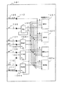
図1に、本発明の一実施例のメモリモジュールを示す。図1において、メモリモジュール101には、kビット幅のデータ信号をもつm個の省消費電力対応型同期型メモリデバイス102−1〜102−m、1つのPLL回路103、および複数の出力制御機能付きレジスタ104−1〜104−nが搭載されている。該メモリモジュール101のインターフェイスは、(m×k)ビット幅のデータ信号線105、1ビットのクロック信号線106、1ビットのクロックイネーブル信号線107、1ビットのチップセレクト信号線108、pビットのアドレス信号線109、qビットのコマンド信号線110および(n−1)ビットのレジスタ出力イネーブル信号線111から構成される。図2とは、レジスタ104−1〜104−nを出力制御機能付きレジスタとし、レジスタ出力イネーブル信号線111を新規に追加した点が相違している。レジスタ出力イネーブル信号線111は、クロックイネーブル信号線107およびチップセレクト信号線108と同様にメモリモジュール毎に用意する。
【0013】
(m×k)ビット幅のデータ信号線105はkビットずつ直接m個の省消費電力対応型同期型メモリデバイス102−1〜102−mへ1:1で接続される。1ビットのクロック信号線106はPLL回路103へ接続され、該PLL回路103の複数ある出力ポートからm個の省消費電力型同期型メモリデバイス102−1〜102−mおよびn個の出力制御機能付きレジスタ104−1〜104−nへ1:1または1:2程度の負荷数で接続される。1ビットのクロックイネーブル信号線107および1ビットのチップセレクト信号線108は、出力イネーブル信号入力ポート(OE)が“H”固定の出力制御機能付きレジスタ204−1へ接続される。該出力制御機能付きレジスタ204−1は、出力イネーブル信号入力ポートを“H”固定とすることで、図2のレジスタ204−1と同様の働きをすることになる。クロックイネーブルとチップセレクトの2つの信号線107、108が特殊扱いなのは、図3のタイミングチャートに示したように、アドレス信号(adr)およびコマンド信号(cmd)がチップセレクト信号(cs#)をアサートしている期間のみアサートすれば良いのに対し、チップセレクト信号はメモリデバイスへのコマンド信号発行時にアサート、非発行時にはディアサートを保証しなければならないためである。クロックイネーブル信号(cke)もチップセレクト信号と同様に、メモリアクセス期間中にはアサート、PowerDownMode期間中にはディアサートを保証しなければならない。pビットのアドレス信号線109およびqビットのコマンド信号線110は各出力制御機能付きレジスタ104−2〜104−nへ接続される。該出力制御機能付きレジスタ104−2〜104−nの出力イネーブル信号入力ポート(OE)に、(n−1)ビットのレジスタ出力イネーブル信号線(図中のregoe)111を1:1の負荷数で接続する。各レジスタ104−1〜104−nの出力ポートからm個の省消費電力対応型同期型メモリデバイス102−1〜102−mへは1:mの負荷数で接続される。
【0014】
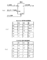
図5に、本実施例で用いる出力制御機能付きレジスタ(REGA)の真理値表を示す。(a)は出力制御機能付きレジスタ(REGA)の入出力信号関係、(b)は出力イネーブル信号がクロック非同期のときの真理値表、(c)はクロック同期のときの真理値表を表わしている。図5に示すように、出力制御機能付きレジスタは、出力イネーブル(以降OE:OutputEnable)信号が“H”の時には出力制御機能無しレジスタと同等の動作をし、OE信号が“L”の時には入力信号が“H/L”いずれの場合においても出力は“L”固定となる。なお、本発明において、OE信号と出力信号のタイミング関係はクロック信号との同期/非同期を問わない。
【0015】
図4と同様に、メモリモジュールがバスにより複数接続された場合の本発明実施例のメモリモジュール101のタイミングチャートを図6および図7に示す。図6は出力制御機能付きレジスタ104−1〜104−nのOE制御がクロック非同期の場合であり、図7は同レジスタ104−1〜104−nのOE制御がクロック同期型のものである。また、(A)はメモリモジュール101の入力インターフェイス信号、(B)はメモリデバイス102−1〜102−mの入力インターフェイス信号を示している。図6の場合、レジスタ出力イネーブル信号(図中のregoe)のアサートタイミングはRASタイミングと同時であり、ディアサートタイミングはCASタイミングから2cycle遅れたタイミングである。図7の場合、レジスタ出力イネーブル信号のアサートタイミングはRASタイミングより1cycle早いタイミングであり、ディアサートタイミングは図6と同様にCASタイミングから2cycle遅れたタイミングである。図6および図7のどちらにおいても、クロックイネーブル信号(図中のcke)と同タイミングでアサートおよびディアサートしても問題ない。逆に、クロックイネーブル信号と同一タイミングであれば、メモリコントローラ側の制御も簡略化可能である。
【0016】
図4に示したように、従来のメモリモジュールでは、メモリモジュールがバスにより複数接続された場合、自メモリモジュールへのコマンドが発生しない場合でも、他メモリモジュールのコマンドが発生した場合、レジスタがコマンド信号およびアドレス信号をセンスして、メモリデバイスまでコマンド信号およびアドレス信号を伝播させてしまうため、レジスタにおいて電力を消費していた。一方、図6および図7から明らかなように、本実施例においては、自メモリモジュールへのコマンドが発生しない期間では、レジスタ出力イネーブル信号(図中のregoe)を“L”とすることにより(OE信号がL)、レジスタの出力は“L”固定となるため、レジスタがコマンド信号およばアドレス信号をセンスしてメモリデバイスまで伝播させてしまうことはなくなり、即ち、レジスタが不要な信号で駆動されることはなくなり、レジスタでの消費電力を抑えることが可能となる。
【0017】
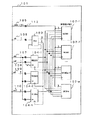
図8に本発明のメモリモジュールの他の実施例を示す。図1との相違点は、出力制御機能付きレジスタのタイプを変更し、OE信号が“L”のときに“L”固定値を出力するのではなく、“Hi−Z”を出力するレジスタ804−1〜804−nにした点である。該出力制御機能付きレジスタ(REGB)の真理値表を図9に示す。図5と同様に、(a)はレジスタの入出力信号関係、(b)は出力イネーブル信号がクロック非同期のときの真理値表、(c)はクロック同期のときの真理値表を表わしている。
【0018】
本実施例においては、レジスタ804−2〜804−nの出力が“Hi−Z”となった場合、省消費電力対応型同期型メモリデバイス102−1〜102−mの入力ポートも“Hi−Z”となり、入力バッファにて貫通電流が流れる等の問題が起こるため、終端抵抗812および終端電圧813にて信号線を終端する。図8では、信号線の波形品質を向上させるために信号線を両端で終端している。信号線の波形品質が問われない場合には片側終端でも良い。片側終端時の構成図を図10に示す。
【0019】
図1や図8の実施例の説明では、出力制御機能付きレジスタの出力イネーブル信号の極性を正極性のものを使用したが、負極性のものを使用してもよい。出力イネーブル信号が正極性とは、出力イネーブル信号が“H”のときに入力信号をクロック信号の立ち上がりエッジでラッチしたものを出力信号とし、出力イネーブル信号が“L”のときには出力信号を“L”固定もしくは“Hi−Z”固定とするものである。逆に、出力イネーブル信号が負極性とは、出力イネーブル信号が”L”のときに入力信号をクロック信号の立ち上がりエッジでラッチしたものを出力信号とし、“H”のときには出力信号を“L”固定もしくは“Hi−Z”固定とするものである。
【0020】
図5のレジスタの負極性版の真理値表を図11に、図9のレジスタの負極性版の真理値表を図12に示す。図5や図9と同様に、(a)はレジスタの入出力信号関係、(b)は出力イネーブル信号がクロック非同期のときの真理値表、(c)はクロック同期のときの真理値表を表わしている。
【0021】
図1、図8および図10のレジスタを正極性から負極性に置き換えたメモリモジュールの構成図を、それぞれ図13、図14および図15に示す。これら実施例のメモリアクセスタイミングチャートは、図6や図7において、レジスタ出力イネーブル信号(図中のregoe)の極性が逆となる以外、基本的に図6や図7と同様である。
【0022】
本発明のメモリモジュールの更に他の実施例を図16に示す。図1との相違点は、出力制御機能付きレジスタ104−2〜104−nの出力イネーブル信号入力ポートには新規に追加したレジスタ出力イネーブル信号線ではなく、もともと存在するクロックイネーブル信号線107を1:(N−1)の負荷数で接続している点にある。即ち、レジスタ出力イネーブル信号線はクロックイネーブル信号線と同様に各メモリモジュール毎に用意し、しかも、基本的に両者のタイミング関係は同じであるため、クロックイネーブル信号線をレジスタ出力イネーブル信号線に兼用しても同様の機能が実現できる。
【0023】
図16の場合、図1のレジスタ出力イネーブル信号線111というのは不要であるため、従来のメモリモジュールに対して部品の載せ替えおよび信号線の接続し直しが起こるだけで、ピンを追加するというような変更はない。なお、図16ではクロックイネーブル信号線107のメモリモジュールのエッジとダンピング抵抗間から信号分岐点をとっているが、ダンピング抵抗とレジスタ間から信号分岐点をとってもよい。その構成図を図17に示す。もちろん各信号線にダンピング抵抗が挿入されなければ図16と図17は同一のものである。
【0024】
図16で示したレジスタのタイプを図9のタイプに変更して両側で終端した場合のメモリモジュールの構成図を図18に示す。また、この図18に対し、図17同様にクロックイネーブル信号線の分岐点をダンピング抵抗とレジスタ間に設定した場合のメモリモジュールの構成図を図19に示す。更に、レジスタ出力信号線を片側で終端した場合のメモリモジュールの構成図を図20と図21に示す。
【0025】
本発明のメモリモジュールの更に他の実施例を図22に示す。図16および図17との相違点は、出力制御機能付きレジスタ104−2〜104−nの出力イネーブル信号入力ポートには、メモリモジュール101に入力されるクロックイネーブル信号線107もしくはダンピング抵抗通過後のクロックイネーブル信号線を接続するものではなく、クロックイネーブル信号線107が入力されるレジスタ104−1の出力信号線を接続する点にある。この場合、クロックイネーブル信号線の負荷数は図1と同じであるために、メモリモジュールとメモリコントローラ間のタイミング設計が容易となる。クロックイネーブル信号線のレジスタ出力の負荷数はm個から(m+n)個に増大するが、メモリモジュール内で閉じている話のためタイミング設計は難しくない。
【0026】
図22で示したレジスタのタイプを図9のタイプに変更して両側を終端した場合のメモリモジュールの構成図を図23に示す。また、レジスタ出力信号線を片側で終端した場合のメモリモジュールの構成図を図24に示す。
【0027】
上記実施例では、レジスタの“L”固定となるものを使用しているが、レジスタの出力値が“H”固定となるものを用いても構成可能である。
【0028】
また、新規に追加するレジスタ出力イネーブル信号の本数はメモリモジュール上のレジスタの個数がn個の場合(n−1)本使用しているが、本数を1本にしてメモリモジュール上で1:(n−1)の負荷数で接続してもよいし、本数を1本から(n−1)本の間に設定し、(n−1)個のレジスタには必ず接続されるようにしてもよい。
【0029】
また、上記実施例では、クロック信号線、クロックイネーブル信号線およびチップセレクト信号線のビット数を1にしているが、負荷分散のために同じ意味(信号線のL、Hのタイミングが同一)となる複数の信号線を用意してもよい。
【0030】
さらに、クロックイネーブル信号線とチップセレクト信号線の性質から、図16から図24の構成において、クロックイネーブル信号線やそのレジスタ出力信号線ではなく、チップセレクト信号線やそのレジスタ出力信号線を、出力制御機能付きレジスタ104−2〜104−nや804−2〜804−nの出力イネーブル信号入力ポートに接続して、該レジスタを制御するようにしてもよい。
【0031】
【発明の効果】
以上説明したように、本発明では、メモリモジュール上のレジスタを出力制御機能付きレジスタへ変更し、メモリアクセスが発生していないときに該レジスタの出力値を固定することにより、レジスタでの消費電力を抑えることが可能である。
【図面の簡単な説明】
【図1】本発明のメモリモジュールの一実施例の構成図である。
【図2】従来のレジスタドタイプのメモリモジュールの構成図である。
【図3】図2のメモリモジュール内のタイミングチャートである。
【図4】図2のメモリモジュールをバス接続したときのタイミングチャートである。
【図5】図1の実施例の出力制御機能付きレジスタの真理値表である。
【図6】図1のメモリモジュールのタイミングチャートである。
【図7】図1のメモリモジュールの別のタイミングチャートである。
【図8】本発明のメモリモジュールの他の実施例の構成図である。
【図9】図8の実施例の出力制御機能付きレジスタの真理値表である。
【図10】本発明のメモリモジュールの更に他の実施例の構成図である。
【図11】図5の出力イネーブル信号負極性版レジスタの真理値表である。
【図12】図9の出力イネーブル信号負極性版レジスタの真理値表である。
【図13】図1のレジスタを図11のレジスタで置き換えたメモリモジュールの構成図である。
【図14】図8のレジスタを図12のレジスタで置き換えたメモリモジュールの構成図である。
【図15】図9のレジスタを図12のレジスタで置き換えたメモリモジュールの構成図である。
【図16】本発明のメモリモジュールの更に他の実施例の構成図である。
【図17】図16の信号分岐点を変更したメモリモジュールの構成図である。
【図18】図16のレジスタを図8のレジスタで置き換えたメモリモジュールの構成図である。
【図19】図17のレジスタを図8のレジスタで置き換えたメモリモジュールの構成図である。
【図20】図16のレジスタを図8のレジスタで置き換えたメモリモジュールの構成図である。
【図21】図17のレジスタを図8のレジスタで置き換えたメモリモジュールの構成図である。
【図22】本発明のメモリモジュールの更に他の実施例の構成図である。
【図23】図22のレジスタを図8のレジスタで置き換えたメモリモジュールの構成図である。
【図24】図22のレジスタを図8のレジスタで置き換えたメモリモジュールの構成図である。
【図25】メモリモジュールがバスにより複数接続されたメモリシステムのブロック図である。
【符号の説明】
100 メモリコントローラ
101 メモリモジュール
102−1〜102m 省消費電力対応型同期型メモリデバイス
103 PLL回路
104−1〜104n 出力イネーブル制御機能付きレジスタ
105 データ信号線
106 クロック信号線
107 クロックイネーブル信号線
108 チップセレクト信号線
109 アドレス信号線
110 コマンド信号線
111 レジスタ出力イネーブル信号線
112 ダンピング抵抗[0001]
BACKGROUND OF THE INVENTION
The present invention relates to a memory module of a computer system such as a personal computer, a workstation, an office computer, and the like, and in particular, a memory module capable of saving power consumption of a memory device and a power consumption of a mounted register, and a computer equipped with the memory module. About the system .
[0002]
[Prior art]
In general, in a memory configuration of a computer system, a flexible change of the memory configuration is realized by using a memory module in which a plurality of memory devices are collected. Since general memory modules are standardized by JEDEC (Joint Electron Device Engineering Council), which is a standardization organization for semiconductor devices, compatibility problems due to differences in memory module vendors do not occur.
[0003]
On the other hand, with the recent increase in speed and scale of computer systems, power consumption in memory systems has become a problem. Although the maximum memory capacity required by computer systems is increasing more and more, the memory that is operating instantaneously is only a part of it. Therefore, in order to counter the problem of power consumption of the memory module, a clock enable signal is added to the memory device to provide a power saving function. A synchronous memory device having this function is called a power-saving synchronous memory device. When the clock enable signal is “H”, normal operation is performed, and when the clock enable signal is “L”, a power saving state called PowerDownMode is established. At the time of PowerDownMode, power consumption can be suppressed to about 1/10 of the normal operation.
[0004]
FIG. 2 shows an example of this type of conventional memory module configuration. The
[0005]
FIG. 3 shows a timing chart of the conventional register type memory module of FIG. FIG. 3 is a timing chart of data writing to a memory in an SDRAM (Synchronous Dynamic Ramdom Access Memory) module. (A) is an input interface signal of the
[0006]
In a memory system considering power consumption, when there is no access to the memory, the clock enable signal is set to “L” to set PowerDownMode, and the clock enable signal is set to “H” immediately before the memory access to return to the normal state. At the time when the memory access is completed, the clock enable signal is set to “L” to set PowerDownMode.
[0007]
As described above, in the conventional registered type memory module shown in FIG. 2, it is possible to suppress the power consumption of the synchronous memory device corresponding to the power saving by controlling the clock enable signal. It is not possible to reduce the power consumption of the register mounted on the PC. Therefore, as shown in FIG. 25, when a plurality of the memory modules are connected by a bus, even if a command to the own memory module is not generated, a register on the own memory module is generated when a command to the other memory module is generated. Senses command and address signals and consumes power in the register.
[0008]
FIG. 4 shows a timing chart of a certain memory module when a plurality of conventional registered type memory modules are connected by a bus. As shown in FIG. 25, the clock enable
[0009]
[Problems to be solved by the invention]
As described above, in the conventional registered type memory module, it is possible to reduce the power consumption of the memory device by adding a clock enable signal and making the memory device compatible with power saving. No consideration is given to reducing the power consumption of the registers mounted on the module.
[0010]
An object of the present invention is to provide a memory module in which a power saving function is applied to a register in addition to a memory device on the memory module, and a computer system including the memory module.
[0011]
[Means for Solving the Problems]
In order to achieve the above object, in the present invention, at least a part of the registers mounted on the memory module is changed to a register with an output control function, and when the register output value is unnecessary, the output value of the register is changed to “L”. "Or" H "means for fixing. As a result, the register does not drive unnecessary signals, and power consumption in the register can be suppressed. For the output enable control of the register with the output control function, a newly added register output enable signal line is used, or a clock enable signal line for controlling the power consumption of the memory device, and further a chip select signal line is used. It is possible to use both.
[0012]
DETAILED DESCRIPTION OF THE INVENTION
FIG. 1 shows a memory module according to an embodiment of the present invention. In FIG. 1, a
[0013]
The data signal
[0014]
FIG. 5 shows a truth table of the register with output control function (REGA) used in this embodiment. (A) is a relation between input and output signals of the register with output control function (REGA), (b) is a truth table when the output enable signal is asynchronous to the clock, and (c) is a truth table when the clock is synchronous. Yes. As shown in FIG. 5, the register with the output control function operates in the same manner as the register without the output control function when the output enable (hereinafter referred to as OE) signal is “H”, and is input when the OE signal is “L”. The output is fixed at “L” regardless of whether the signal is “H / L”. In the present invention, the timing relationship between the OE signal and the output signal may be synchronous / asynchronous with the clock signal.
[0015]
Similar to FIG. 4, timing charts of the
[0016]
As shown in FIG. 4, in the conventional memory module, when a plurality of memory modules are connected by a bus, even if a command to the own memory module is not generated, a command is issued when a command of another memory module is generated. Since the signal and the address signal are sensed and the command signal and the address signal are propagated to the memory device, power is consumed in the register. On the other hand, as is apparent from FIGS. 6 and 7, in the present embodiment, the register output enable signal (rego in the figure) is set to “L” during the period when the command to the own memory module is not generated ( Since the OE signal is L) and the output of the register is fixed to “L”, the register does not sense and propagate the command signal and address signal to the memory device, that is, the register is driven with an unnecessary signal. Thus, the power consumption in the register can be suppressed.
[0017]
FIG. 8 shows another embodiment of the memory module of the present invention. The difference from FIG. 1 is that the type of the register with the output control function is changed, and when the OE signal is “L”, a fixed value “L” is not output, but a
[0018]
In this embodiment, when the outputs of the registers 804-2 to 804-n become “Hi-Z”, the input ports of the power-saving synchronous memory devices 102-1 to 102-m are also “Hi−”. Z ″, and a problem such as a through current flowing in the input buffer occurs. Therefore, the signal line is terminated by the
[0019]
In the description of the embodiment in FIGS. 1 and 8, the polarity of the output enable signal of the register with the output control function is positive, but a negative polarity may be used. The output enable signal is positive when the output enable signal is “H” and the input signal is latched at the rising edge of the clock signal as an output signal. When the output enable signal is “L”, the output signal is “L”. "Fixed" or "Hi-Z" fixed. On the other hand, the negative polarity of the output enable signal means that when the output enable signal is “L”, the input signal is latched at the rising edge of the clock signal, and when it is “H”, the output signal is “L”. Fixed or “Hi-Z” fixed.
[0020]
FIG. 11 shows a truth table of the negative polarity version of the register of FIG. 5, and FIG. 12 shows a truth table of the negative polarity version of the register of FIG. Like FIG. 5 and FIG. 9, (a) shows the relationship between the input and output signals of the register, (b) shows a truth table when the output enable signal is asynchronous to the clock, and (c) shows a truth table when the clock is synchronous. It represents.
[0021]
Configuration diagrams of memory modules in which the registers of FIGS. 1, 8, and 10 are replaced from positive polarity to negative polarity are shown in FIGS. 13, 14, and 15, respectively. The memory access timing charts of these embodiments are basically the same as those of FIGS. 6 and 7 except that the polarity of the register output enable signal (rego in the figure) is reversed in FIGS.
[0022]
Still another embodiment of the memory module of the present invention is shown in FIG. 1 is different from the newly added register output enable signal line in the output enable signal input port of the registers 104-2 to 104-n with output control function, in that the clock enable
[0023]
In the case of FIG. 16, the register output enable signal line 111 of FIG. 1 is not necessary, so that a pin is added only by changing parts and reconnecting signal lines to the conventional memory module. There is no such change. In FIG. 16, the signal branch point is taken from between the edge of the memory module of the clock enable
[0024]
FIG. 18 shows a configuration diagram of the memory module when the register type shown in FIG. 16 is changed to the type shown in FIG. 9 and terminated on both sides. FIG. 19 is a block diagram of the memory module when the branch point of the clock enable signal line is set between the damping resistor and the register as in FIG. Further, FIG. 20 and FIG. 21 show the configuration of the memory module when the register output signal line is terminated on one side.
[0025]
Another embodiment of the memory module of the present invention is shown in FIG. The difference from FIGS. 16 and 17 is that the output enable signal input ports of the registers 104-2 to 104-n with output control function are connected to the clock enable
[0026]
FIG. 23 shows a configuration diagram of the memory module when the register type shown in FIG. 22 is changed to the type shown in FIG. 9 and both sides are terminated. FIG. 24 shows a configuration diagram of the memory module when the register output signal line is terminated on one side.
[0027]
In the above-described embodiment, a register whose value is fixed to “L” is used, but it is also possible to use a register whose output value is fixed to “H”.
[0028]
Further, the number of register output enable signals to be newly added is used when the number of registers on the memory module is n (n-1). However, the number of register output enable signals is 1 :( The number of loads may be n-1), or the number may be set between 1 and (n-1) so that the number of registers is always connected to (n-1). Good.
[0029]
In the above embodiment, the number of bits of the clock signal line, the clock enable signal line, and the chip select signal line is set to 1, but the same meaning (the timings of L and H of the signal lines are the same) for load distribution. A plurality of signal lines may be prepared.
[0030]
Further, due to the nature of the clock enable signal line and the chip select signal line, the chip select signal line and its register output signal line are output instead of the clock enable signal line and its register output signal line in the configuration of FIGS. The registers may be controlled by connecting to the output enable signal input ports of the registers 104-2 to 104-n and 804-2 to 804-n with control function.
[0031]
【The invention's effect】
As described above, in the present invention, by changing the register on the memory module to a register with an output control function, and fixing the output value of the register when no memory access occurs, the power consumption in the register Can be suppressed.
[Brief description of the drawings]
FIG. 1 is a configuration diagram of an embodiment of a memory module of the present invention.
FIG. 2 is a configuration diagram of a conventional registered type memory module;
FIG. 3 is a timing chart in the memory module of FIG. 2;
4 is a timing chart when the memory module of FIG. 2 is connected by a bus. FIG.
5 is a truth table of a register with an output control function of the embodiment of FIG.
6 is a timing chart of the memory module of FIG. 1. FIG.
FIG. 7 is another timing chart of the memory module of FIG. 1;
FIG. 8 is a configuration diagram of another embodiment of a memory module of the present invention.
9 is a truth table of a register with an output control function of the embodiment of FIG.
FIG. 10 is a configuration diagram of still another embodiment of the memory module of the present invention.
11 is a truth table of the output enable signal negative polarity version register of FIG. 5;
FIG. 12 is a truth table of the output enable signal negative polarity version register of FIG. 9;
13 is a configuration diagram of a memory module in which the register of FIG. 1 is replaced with the register of FIG.
14 is a configuration diagram of a memory module in which the register of FIG. 8 is replaced with the register of FIG. 12;
15 is a configuration diagram of a memory module in which the register of FIG. 9 is replaced with the register of FIG.
FIG. 16 is a configuration diagram of still another embodiment of the memory module of the present invention.
17 is a configuration diagram of a memory module in which the signal branch point of FIG. 16 is changed.
18 is a configuration diagram of a memory module in which the register of FIG. 16 is replaced with the register of FIG.
19 is a configuration diagram of a memory module in which the register of FIG. 17 is replaced with the register of FIG.
20 is a configuration diagram of a memory module in which the register of FIG. 16 is replaced with the register of FIG.
21 is a configuration diagram of a memory module in which the register of FIG. 17 is replaced with the register of FIG.
FIG. 22 is a block diagram of still another embodiment of the memory module of the present invention.
23 is a configuration diagram of a memory module in which the register of FIG. 22 is replaced with the register of FIG.
24 is a configuration diagram of a memory module in which the register of FIG. 22 is replaced with the register of FIG.
FIG. 25 is a block diagram of a memory system in which a plurality of memory modules are connected by a bus.
[Explanation of symbols]
DESCRIPTION OF
Claims (4)
前記複数のレジスタの少なくとも一部のレジスタは出力制御機能付きレジスタで構成されると共に、前記出力制御機能付きレジスタの出力値を制御するための信号線を有し、
前記出力制御機能付きレジスタによる前記メモリデバイスへの入力信号が不要時に、前記信号線により当該出力制御機能付きレジスタの出力値を“L”もしくは“H”に固定して、レジスタでの消費電力を抑えることを特徴とする省消費電力型メモリモジュール。A plurality of power-saving memory devices, a PLL circuit that outputs a phase-adjusted clock, and a plurality of buffers for latching and buffering an input signal to the memory device using an output clock of the PLL circuit as a trigger in the power saving types memory module and a register,
Together with at least a portion of the register is constituted by the output control function register of the plurality of registers has a signal line for controlling the output value of the output control function register,
When an input signal to the memory device by the register with the output control function is unnecessary, the output value of the register with the output control function is fixed to “L” or “H” by the signal line, and the power consumption in the register is reduced. A power-saving memory module characterized by being suppressed .
Priority Applications (1)
| Application Number | Priority Date | Filing Date | Title |
|---|---|---|---|
| JP2000178105A JP4717983B2 (en) | 2000-06-14 | 2000-06-14 | Power-saving memory module and computer system |
Applications Claiming Priority (1)
| Application Number | Priority Date | Filing Date | Title |
|---|---|---|---|
| JP2000178105A JP4717983B2 (en) | 2000-06-14 | 2000-06-14 | Power-saving memory module and computer system |
Publications (3)
| Publication Number | Publication Date |
|---|---|
| JP2001357672A JP2001357672A (en) | 2001-12-26 |
| JP2001357672A5 JP2001357672A5 (en) | 2007-07-26 |
| JP4717983B2 true JP4717983B2 (en) | 2011-07-06 |
Family
ID=18679592
Family Applications (1)
| Application Number | Title | Priority Date | Filing Date |
|---|---|---|---|
| JP2000178105A Expired - Fee Related JP4717983B2 (en) | 2000-06-14 | 2000-06-14 | Power-saving memory module and computer system |
Country Status (1)
| Country | Link |
|---|---|
| JP (1) | JP4717983B2 (en) |
Families Citing this family (3)
| Publication number | Priority date | Publication date | Assignee | Title |
|---|---|---|---|---|
| WO2004003758A1 (en) * | 2002-07-01 | 2004-01-08 | Hitachi, Ltd. | Directional coupling bus system |
| JP5486812B2 (en) * | 2009-01-09 | 2014-05-07 | 株式会社メガチップス | Memory control circuit |
| JP5668559B2 (en) * | 2011-03-22 | 2015-02-12 | 日本電気株式会社 | Information processing apparatus, control method thereof, and program |
Citations (6)
| Publication number | Priority date | Publication date | Assignee | Title |
|---|---|---|---|---|
| JPS51128234A (en) * | 1975-04-30 | 1976-11-09 | Toshiba Corp | Mos-type semi-conductor memory |
| JPS5891591A (en) * | 1981-11-27 | 1983-05-31 | Toshiba Corp | Power saving system of semiconductor memory |
| JPS61105795A (en) * | 1984-10-29 | 1986-05-23 | Nec Corp | Memory circuit |
| JPS63239691A (en) * | 1980-02-04 | 1988-10-05 | テキサス インスツルメンツ インコ−ポレイテツド | Semiconductor memory buffer |
| JPH01201890A (en) * | 1988-02-05 | 1989-08-14 | Fujitsu Ltd | Read only memory control circuit |
| JPH1186526A (en) * | 1997-09-12 | 1999-03-30 | Nec Eng Ltd | Memory controller |
Family Cites Families (3)
| Publication number | Priority date | Publication date | Assignee | Title |
|---|---|---|---|---|
| JPH0377158A (en) * | 1989-08-18 | 1991-04-02 | Mitsubishi Electric Corp | Microprocessor |
| JP3189875B2 (en) * | 1997-06-04 | 2001-07-16 | 日本電気株式会社 | State machine |
| JP2000195287A (en) * | 1998-12-28 | 2000-07-14 | Hitachi Ltd | Shift register, serial/parallel conversion circuit, and lsi for communication |
-
2000
- 2000-06-14 JP JP2000178105A patent/JP4717983B2/en not_active Expired - Fee Related
Patent Citations (6)
| Publication number | Priority date | Publication date | Assignee | Title |
|---|---|---|---|---|
| JPS51128234A (en) * | 1975-04-30 | 1976-11-09 | Toshiba Corp | Mos-type semi-conductor memory |
| JPS63239691A (en) * | 1980-02-04 | 1988-10-05 | テキサス インスツルメンツ インコ−ポレイテツド | Semiconductor memory buffer |
| JPS5891591A (en) * | 1981-11-27 | 1983-05-31 | Toshiba Corp | Power saving system of semiconductor memory |
| JPS61105795A (en) * | 1984-10-29 | 1986-05-23 | Nec Corp | Memory circuit |
| JPH01201890A (en) * | 1988-02-05 | 1989-08-14 | Fujitsu Ltd | Read only memory control circuit |
| JPH1186526A (en) * | 1997-09-12 | 1999-03-30 | Nec Eng Ltd | Memory controller |
Also Published As
| Publication number | Publication date |
|---|---|
| JP2001357672A (en) | 2001-12-26 |
Similar Documents
| Publication | Publication Date | Title |
|---|---|---|
| US9304579B2 (en) | Fast-wake memory control | |
| US6141283A (en) | Method and apparatus for dynamically placing portions of a memory in a reduced power consumption state | |
| US5835435A (en) | Method and apparatus for dynamically placing portions of a memory in a reduced power consumtion state | |
| US9666250B2 (en) | Memory signal buffers and modules supporting variable access granularity | |
| US9229523B2 (en) | Memory controller with transaction-queue-dependent power modes | |
| US5448715A (en) | Dual clock domain interface between CPU and memory bus | |
| JP3960583B2 (en) | Semiconductor memory device and system having memory module including the same | |
| KR100588599B1 (en) | Memory module and memory system | |
| US8065461B2 (en) | Capturing read data | |
| US20030105932A1 (en) | Emulation of memory clock enable pin and use of chip select for memory power control | |
| US20020156953A1 (en) | Dynamic bus inversion method | |
| US20100257335A1 (en) | Reconfigurable circuit with suspension control circuit | |
| US7405995B2 (en) | Semiconductor storage device | |
| US5625847A (en) | High-speed ISA bus control system for changing command cycle execution speed by selectively using ISA bus controller and high-speed bus controller | |
| US5901322A (en) | Method and apparatus for dynamic control of clocks in a multiple clock processor, particularly for a data cache | |
| US6487617B1 (en) | Source-destination re-timed cooperative communication bus | |
| US6452865B1 (en) | Method and apparatus for supporting N-bit width DDR memory interface using a common symmetrical read data path with 2N-bit internal bus width | |
| JP4717983B2 (en) | Power-saving memory module and computer system | |
| US7165184B2 (en) | Transferring data between differently clocked busses | |
| EP1141832B1 (en) | Regulating a data transfer time | |
| US7155630B2 (en) | Method and unit for selectively enabling an input buffer based on an indication of a clock transition | |
| JP2000163959A (en) | Semiconductor storage device | |
| KR20050119688A (en) | A virtual dual-port synchronous ram architecture | |
| US6154820A (en) | Arrangement for storing program instructions and data in a memory device and method therefor | |
| GB2379542A (en) | System comprising a memory module |
Legal Events
| Date | Code | Title | Description |
|---|---|---|---|
| A521 | Written amendment |
Free format text: JAPANESE INTERMEDIATE CODE: A523 Effective date: 20070611 |
|
| A621 | Written request for application examination |
Free format text: JAPANESE INTERMEDIATE CODE: A621 Effective date: 20070611 |
|
| A131 | Notification of reasons for refusal |
Free format text: JAPANESE INTERMEDIATE CODE: A131 Effective date: 20100630 |
|
| A521 | Written amendment |
Free format text: JAPANESE INTERMEDIATE CODE: A523 Effective date: 20100830 |
|
| A01 | Written decision to grant a patent or to grant a registration (utility model) |
Free format text: JAPANESE INTERMEDIATE CODE: A01 Effective date: 20110316 |
|
| A01 | Written decision to grant a patent or to grant a registration (utility model) |
Free format text: JAPANESE INTERMEDIATE CODE: A01 |
|
| A61 | First payment of annual fees (during grant procedure) |
Free format text: JAPANESE INTERMEDIATE CODE: A61 Effective date: 20110331 |
|
| R150 | Certificate of patent or registration of utility model |
Free format text: JAPANESE INTERMEDIATE CODE: R150 |
|
| FPAY | Renewal fee payment (event date is renewal date of database) |
Free format text: PAYMENT UNTIL: 20140408 Year of fee payment: 3 |
|
| LAPS | Cancellation because of no payment of annual fees |