JP4712974B2 - Flexible probe / probe response path control for coherency maintenance - Google Patents
Flexible probe / probe response path control for coherency maintenance Download PDFInfo
- Publication number
- JP4712974B2 JP4712974B2 JP2000590061A JP2000590061A JP4712974B2 JP 4712974 B2 JP4712974 B2 JP 4712974B2 JP 2000590061 A JP2000590061 A JP 2000590061A JP 2000590061 A JP2000590061 A JP 2000590061A JP 4712974 B2 JP4712974 B2 JP 4712974B2
- Authority
- JP
- Japan
- Prior art keywords
- node
- probe
- response
- data
- packet
- Prior art date
- Legal status (The legal status is an assumption and is not a legal conclusion. Google has not performed a legal analysis and makes no representation as to the accuracy of the status listed.)
- Expired - Fee Related
Links
Images


Classifications
-
- G—PHYSICS
- G06—COMPUTING; CALCULATING OR COUNTING
- G06F—ELECTRIC DIGITAL DATA PROCESSING
- G06F12/00—Accessing, addressing or allocating within memory systems or architectures
- G06F12/02—Addressing or allocation; Relocation
- G06F12/08—Addressing or allocation; Relocation in hierarchically structured memory systems, e.g. virtual memory systems
- G06F12/0802—Addressing of a memory level in which the access to the desired data or data block requires associative addressing means, e.g. caches
- G06F12/0806—Multiuser, multiprocessor or multiprocessing cache systems
- G06F12/0815—Cache consistency protocols
-
- G—PHYSICS
- G06—COMPUTING; CALCULATING OR COUNTING
- G06F—ELECTRIC DIGITAL DATA PROCESSING
- G06F13/00—Interconnection of, or transfer of information or other signals between, memories, input/output devices or central processing units
- G06F13/14—Handling requests for interconnection or transfer
- G06F13/16—Handling requests for interconnection or transfer for access to memory bus
- G06F13/1605—Handling requests for interconnection or transfer for access to memory bus based on arbitration
- G06F13/1652—Handling requests for interconnection or transfer for access to memory bus based on arbitration in a multiprocessor architecture
- G06F13/1663—Access to shared memory
-
- G—PHYSICS
- G06—COMPUTING; CALCULATING OR COUNTING
- G06F—ELECTRIC DIGITAL DATA PROCESSING
- G06F12/00—Accessing, addressing or allocating within memory systems or architectures
- G06F12/02—Addressing or allocation; Relocation
- G06F12/08—Addressing or allocation; Relocation in hierarchically structured memory systems, e.g. virtual memory systems
- G06F12/0802—Addressing of a memory level in which the access to the desired data or data block requires associative addressing means, e.g. caches
- G06F12/0806—Multiuser, multiprocessor or multiprocessing cache systems
- G06F12/0815—Cache consistency protocols
- G06F12/0817—Cache consistency protocols using directory methods
-
- G—PHYSICS
- G06—COMPUTING; CALCULATING OR COUNTING
- G06F—ELECTRIC DIGITAL DATA PROCESSING
- G06F2212/00—Indexing scheme relating to accessing, addressing or allocation within memory systems or architectures
- G06F2212/25—Using a specific main memory architecture
- G06F2212/254—Distributed memory
-
- G—PHYSICS
- G06—COMPUTING; CALCULATING OR COUNTING
- G06F—ELECTRIC DIGITAL DATA PROCESSING
- G06F2212/00—Indexing scheme relating to accessing, addressing or allocation within memory systems or architectures
- G06F2212/62—Details of cache specific to multiprocessor cache arrangements
- G06F2212/621—Coherency control relating to peripheral accessing, e.g. from DMA or I/O device
Description
【0001】
【発明の背景】
1.技術分野
この発明は広くはコンピュータシステムに関し、より特定的には、マルチプロセッシング演算環境を達成するためのメッセージ通信方式に関する。
【0002】
2.関連技術分野の背景
クメール・A(Kumar A)他による「共有メモリハイパーキューブマイクロプロセッサのための、効率的でスケーラブルなキャッシュコヒーレンス方式(Efficient and Scalable Cache Coherence Schemes for Shared Memory Hypercube Microprocessor)」Proceedings of the Supercomputing Conference、US Los Alamitos、IEEE、Vol.Conf.7. 1994、pp.498-507は、前掲の請求項1のプリアンブルに記載の特徴を有しキャッシュコヒーレンシが維持されるコンピュータシステムと、前掲の請求項10のプリアンブルの特徴を有しコンピュータシステム内でキャッシュコヒーレンシを維持するための方法とを開示する。
EP−A−0 817 076は、ローカルおよびグローバルアドレススペースと、多数のアクセスモードとを用いる、マルチプロセッシングコンピュータシステムを開示する。ノード内のプロセッサは、ノード間通信を要求するトランザクションを開始し得る。要求するノードからホームノードへ要求が送られると、ホームノードは、要求されたデータのキャッシュコピーを有する従属ノードのいずれかに、読出および/または無効化要求を送る。システムは、キャッシュコヒーレンシを維持するためのグローバルコヒーレンシプロトコルを実現化する。
一般的には、パーソナルコンピュータ(PC)およびその他の種類のコンピュータシステムは、メモリにアクセスするために共用バスシステムを中心に設計されてきた。1つ以上のプロセッサおよび1つ以上の入力/出力(I/O)装置が、共用バスを介してメモリに結合される。I/O装置は、共用バスとI/O装置との間の情報の転送を管理するI/Oブリッジを介して共用バスに結合される場合もある一方、プロセッサは典型的には、直接共用バスに結合されるか、またはキャッシュ階層構造を介して共用バスに結合される。
【0003】
残念ながら、共用バスシステムはいくつかの欠点を有する。たとえば、共用バスには多数の装置が装着されることから、バスは典型的には比較的低い周波数で動作される。多数の装着物は、バス上で信号を駆動する装置に容量的な高負荷をもたらし、多数の装着点は、比較的複雑な高周波数に対する伝送ラインモデルをもたらす。したがって、周波数は低く留められ、共用バスで使用できる帯域幅も同様に比較的低い。低帯域幅は共用バスに付加的な装置を装着するのに障壁になり得るが、これは使用できる帯域幅によって性能が制限されるおそれがあるためである。
【0004】
共用バスシステムの他の欠点は、より多くの装置に対するスケーラビリティの欠如である。上述のように、帯域幅が固定される(そして、もし付加的な装置の追加によってバスの動作可能周波数が減じられると、減少し得る)。バスに(直接的にまたは間接的に)装着された装置の帯域幅要件が、一旦バスの利用可能な帯域幅を超えると、装置はバスへのアクセスを試みたときにしばしばストールし得る。全体的な性能が減じられるであろう。
【0005】
上述の問題のうち1つまたはいくつかには、分散メモリシステムを用いて対処し得る。分散メモリシステムを用いるコンピュータシステムは、複数のノードを含む。2つ以上のノードがメモリに接続され、それらのノードは何らかの好適な相互接続を用いて相互接続される。たとえば、ノードの各々は専用ラインを用いて他のノードに互いに接続されることができる。これに代えて、ノードの各々は固定された数の他のノードに接続され、トランザクションは第1のノードから1つ以上の中間ノードを介して、第1のノードに直接接続されていない第2のノードに経路制御されてもよい。メモリアドレス空間は、各々のノードのメモリにわたって割当てられる。
【0006】
ノードはさらに、1つ以上のプロセッサを含み得る。プロセッサは典型的には、メモリから読出したデータのキャッシュブロックをストアするキャッシュを含む。さらに、ノードはプロセッサの外部の1つ以上のキャッシュを含み得る。プロセッサおよび/またはノードは、他のノードからアクセスされるキャッシュブロックをストアし得るために、ノード内のコヒーレンシを維持するための機構が望まれる。
【0007】
【発明の開示】
上に概略を述べた問題は、ここに説明するコンピュータシステムによってほとんどが解決される。このコンピュータシステムは多数の処理ノードを含むことができ、そのうち1つ以上は分散メモリシステムを形成し得る別々のメモリに結合し得る。処理ノードはキャッシュを含むことができ、コンピュータシステムは、キャッシュと分散メモリシステムとの間のコヒーレンシを維持し得る。特に、このコンピュータシステムは柔軟なプローブコマンド/応答経路制御方式を実現化し得る。
【0008】
一実施例においては、この方式はプローブコマンド内の表示を用い、これはプローブ応答を受信する受信ノードを識別する。一般的にはプローブコマンドとは、キャッシュブロックがノード内にストアされているか判断するためのそのノードへの要求であり、かつ、キャッシュブロックがそのノードにストアされていた場合にそのノードが行なうべき動作の表示である。プローブ応答は、動作が行なわれたことを表示し、かつ、キャッシュブロックがノードによって変更されていた場合にはデータの送信を含み得る。送られたコマンドに依存してプローブ応答を異なった受信ノードに経路制御することへ柔軟性を与えることにより、コヒーレンシの維持を比較的効率的な態様で(たとえば最少の数のパケット送信を処理ノード間で用いて)行ない得る一方で、それでもコヒーレンシが維持されることを確実にする。
【0009】
たとえば、ターゲットまたはトランザクションのソースがトランザクションに対応するプローブ応答を受取るべきことを表示するプローブコマンドを含み得る。プローブコマンドは、トランザクションのソースを読出トランザクションに対する受信ノードとして特定し得る(それによりダーティデータをストアするノードからダーティデータがソースノードに引渡される)。一方で、(データがトランザクションのターゲットノードでメモリ内に更新される)書込トランザクションに対しては、プローブコマンドはトランザクションのターゲットを受信ノードとして特定し得る。このようにして、ターゲットはいつ書込データをメモリにコミットするか判断し、書込データとマージされるべきいかなるダーティデータをも受取ることができる。
【0010】
概略的には、コンピュータシステムが企図される。コンピュータシステムは、第1の処理ノードと第2の処理ノードとを含み得る。第1の処理ノードは、要求を送信することによりトランザクションを開始するよう構成し得る。第2の処理ノードは、第1の処理ノードからの要求を受取るよう結合されて、要求に応答してプローブを生成するよう構成し得る。プローブは、プローブに対する応答を受けるための受信ノードを指定する表示を含み得る。さらに、第2の処理ノードはトランザクションのタイプに応答して、表示を生成するよう構成し得る。
【0011】
コンピュータシステム内でのコヒーレンシを維持するための方法もまた企図される。ソースノードからの要求はターゲットノードに送信される。プローブは要求に応答してターゲットノード内で生成される。プローブ内の表示を介して、プローブに対する応答のための受信ノードが指定される。プローブに対するプローブ応答は、受信ノードに経路制御される。
【0012】
この発明の他の目的と利点とは、以下の詳細な説明を読み、添付の図面を参照することにより、より明らかとなるであろう。
【0013】
この発明はさまざまな変形と代替形に対処するものであるが、その特定の実施例を図面において例示の目的で示し、以下に詳述する。しかしながら、図面とその詳細な説明とは開示される発明を特定の形に限定することを意図せず、反対に、すべての変形、等価物、および代替例は前掲の特許請求の範囲に規定されるこの発明の範囲に入ることを意図する。
【0014】
【発明の実施の形態】
例示的なコンピュータシステムの実施例
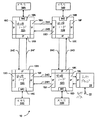
図1は、マルチプロセッシングコンピュータシステム10の一実施例を示す。他の実施例が可能であり企図される。図1の実施例においては、コンピュータシステム10はいくつかの処理ノード12A、12B、12C、および12Dを含む。処理ノードの各々は、処理ノード12A−12Dにそれぞれ含まれるメモリコントローラ16A−16Dを介して、それぞれのメモリ14A−14Dに結合される。さらに、処理ノード12A−12Dは、処理ノード12A−12Dの間の通信のために用いるインターフェイスロジックを含む。たとえば、処理ノード12Aは、処理ノード12Bと通信するためのインターフェイスロジック18Aと、処理ノード12Cと通信するためのインターフェイスロジック18Bと、さらに別の処理ノード(図示せず)と通信するための第3のインターフェイスロジック18Cを含む。同様に、処理ノード12Bはインターフェイスロジック18D、18E、および18Fを含み、処理ノード12Cはインターフェイスロジック18G、18H、および18Iを含み、処理ノード12Dはインターフェイスロジック18J、18K、および18Lを含む。処理ノード12Dは、インターフェイスロジック18Lを介して結合されてI/Oブリッジ20と通信する。他の処理ノードは同様の様式で他のI/Oブリッジと通信し得る。I/Oブリッジ20はI/Oバス22に結合される。
【0015】
処理ノード12A−12Dは、ノード通信相互処理のためのパケットベースのリンクを実現化する。この実施例においては、リンクは単方向ラインの組として実現化される(たとえば、ライン24Aはパケットを処理ノード12Aから処理ノード12Bへ送信するために用いられ、ライン24Bはパケットを処理ノード12Bから処理ノード12Aへ送信するために用いられる)。ライン24C−24Hの他の組は、図1に示すようにパケットを他の処理ノード間で通信するために用いられる。リンクは、処理ノード間の通信のためにキャッシュコヒーレント様式で動作するか、または処理ノードとI/Oブリッジとの間の通信のために非コヒーレント様式で動作し得る。一方の処理ノードから他方へ送信されるべきパケットは、1つ以上の中間ノードを通過し得ることに留意されたい。たとえば、処理ノード12Aから処理ノード12Dに送信されるパケットは、図1に示すように、処理ノード12Bまたは処理ノード12Cのいずれかを通過し得る。いかなる好適な経路制御アルゴリズムをも用い得る。コンピュータシステム10の他の実施例は、図1に示す実施例よりもより多いかまたはより少ない処理ノードを含み得る。
【0016】
処理ノード12A−12Dは、メモリコントローラとインターフェイスロジックに加えて、1つ以上のプロセッサを含み得る。概略的には、処理ノードは少なくとも1つのプロセッサを含み、選択により、メモリおよび所望の他のロジックとの間で通信するためのメモリコントローラを含む。この開示では「ノード」という用語も使用し得る。ノードという用語は、「処理ノード」を意味することを意図する。
【0017】
メモリ14A−14Dは、何らかの好適なメモリ装置を含み得る。たとえば、メモリ14A−14Dは、1つ以上のRAMBUS DRAM(RDRAM)、シンクロナスDRAM(SDRAM)、スタティックRAMなどを含み得る。コンピュータシステム10のアドレス空間は、メモリ14A−14Dの間で分割される。処理ノード12A−12Dの各々はメモリマップを含むことができ、該メモリマップを用いて、どのアドレスがどのメモリにマッピングされているかを判断し、よって、ある特定のアドレスに対するメモリ要求がどの処理ノード12A−12Dに経路制御されるべきかを判断する。一実施例においては、コンピュータシステム10内のアドレスに対するコヒーレンシ点は、アドレスに対応するバイトをストアしているメモリに結合された、メモリコントローラ16A−16Dである。言い換えると、メモリコントローラ16A−16Dは、対応するメモリ14A−14Dへのメモリアクセスの各々を、キャッシュコヒーレントな様式で起こることを確実にすることを担当している。メモリコントローラ16A−16Dは、メモリ14A−14Dにインターフェイスするための制御回路を含み得る。さらに、メモリコントローラ16A−16Dは、メモリ要求を待ち行列として管理するための、要求キューを含み得る。
【0018】
一般的には、インターフェイスロジック18A−18Lは、リンクからのパケットを受取り、かつリンクに送信されるべきパケットをバッファするための、さまざまなバッファを含み得る。コンピュータシステム10は、パケットを転送するための好適なフロー制御であればいずれでも用い得る。たとえば一実施例においては、インターフェイスロジック18の各々は、そのインターフェイスロジックが接続されたリンクの他端のレシーバ内に、いくつかの各種のバッファのカウントをストアする。インターフェイスロジックは、受信インターフェイスロジックがパケットをストアするフリーのバッファを有さない限り、パケットを送信しない。パケットを次に経路制御することにより受信バッファが解放されると、受信インターフェイスロジックは送信インターフェイスロジックにメッセージを送り、バッファが解放されたことを示す。そのような機構は、「クーポンに基づく」システムと呼べる。
【0019】
次に図2は、処理ノード12Aおよび12Bのブロック図を示し、それらの間のリンクの1実施例を詳細に例示する。。図2の実施例においては、ライン24Aは、クロックライン24AAと、制御ライン24ABと、制御/アドレス/データバス24ACとを含む。同様に、ライン24Bは、クロックライン24BAと、制御ライン24BBと、制御/アドレス/データバス24BCとを含む。
【0020】
クロックラインは、制御ラインおよび制御/アドレス/データバスに対するサンプルポイントを示すクロック信号を送信する。特定の一実施例においては、データ/制御ビットはクロック信号のエッジの各々(すなわち立上がりエッジおよび立下がりエッジ)で送信される。したがって、クロックサイクルごとに、ラインごとに2つのデータビットを送信し得る。ラインごとに1ビットを送信するために使用される時間は、ここでは「ビット時間」と呼ぶ。上述の実施例は、クロックサイクルごとに2つのビット時間を含む。パケットは2つ以上のビット時間で送信し得る。制御/アドレス/データバスの幅に依存して、多数のクロックラインを用い得る。たとえば32ビット制御/アドレス/データバスに対しては2つのクロックラインを用い得る(制御/アドレス/データバスの半分では一方のクロックラインが参照され、残りの半分の制御/アドレス/データバスと制御ラインとでは他方のクロックラインが参照される)。一般的には、「パケット」とは2つの処理ノード12A−12Dの間の通信である。1つ以上のパケットが「トランザクション」を形成し得るが、これは一方の処理ノードから他方への情報の転送である。トランザクションを形成するパケットは、ソースノード(転送を要求する開始するノード)からのターゲットノード(トランザクションが向けられるノード)へのトランザクションを開始する要求パケットと、コヒーレンシを維持するために他の処理ノード間で送信されるパケットと、データパケットと、トランザクションを終了させる肯定応答パケットとを含み得る。
【0021】
制御ラインは、制御/アドレス/データバスに送信されたデータが、ビット時間の制御パケットか、またはビット時間のデータパケットであるかを示す。制御ラインはアサートされて制御パケットを示し、デアサートされてデータパケットを示す。ある制御パケットは、後にデータパケットが続くことを示す。データパケットは、対応する制御パケットのすぐ後に続き得る。一実施例においては、他の制御パケットがデータパケットの送信に割込むおそれがある。そのような割込は、データパケットの送信の間に制御ラインをいくつかのビット時間アサートし、かつ制御ラインがアサートされている間にビット時間の制御パケットを送信することにより行なわれる可能性がある。データパケットに割込む制御パケットは、データパケットが後に続くことを示さないおそれがある。
【0022】
制御/アドレス/データバスは、データ/制御ビットを送信するための1組のラインを含む。一実施例においては、制御/アドレス/データバスは、8、16、または32のラインを含み得る。処理ノードまたはI/Oブリッジの各々は、設計選択にしたがってサポートされる数のラインのうちのいずれかを用い得る。他の実施例は、所望により他のサイズの制御/アドレス/データバスをサポートし得る。
【0023】
一実施例によると、コマンド/アドレス/データバスラインおよびクロックラインは、反転データを担持し得る(すなわち、論理1はライン上の低電圧として表わされ、論理0が高電圧として表わされる)。これに代えて、これらのラインは非反転データを担持してもよい(論理1はライン上の高電圧として表わされ、論理0は低電圧として表わされる)。
【0024】
図3から図6は、コンピュータシステム10の一実施例に従って用いられる、例示的なパケットを示す。図3から図5は制御パケットを示し、図6はデータパケットを示す。他の実施例は、所望により異なったパケット定義を用い得る。パケットの各々は、「ビット時間」の見出しの下に列挙される一連のビット時間で示される。パケットのビット時間は、リストされたビット時間順序に従って送信される。図3から図6は、8ビット制御/アドレス/データバス実現化のためのパケットを示す。したがって、ビット時間の各々は、7から0まで番号が付与された8つのビットを含む。図中、いずれの値も付与されていないビットは、所与のパケットのために予約されているか、またはパケット特定情報を送信するために用いられるかのいずれかであり得る。
【0025】
図3は情報パケット(infoパケット)30を示す。情報パケット30は、8ビットリンク上の2つのビット時間を含む。この実施例においては、コマンド符号化はビット時間1の間に送信され、かつ6ビットを含む。図4、および図5に示す他方の制御パケットの各々は、ビット時間1の間に同じビット位置においてコマンド符号化を含む。メッセージがメモリアドレスを含まないときに、情報パケット30を用いてこのメッセージを処理ノード間で送信し得る。
【0026】
図4はアドレスパケット(addressパケット)32を示す。アドレスパケット32は、8ビットリンク上の8つのビット時間を含む。コマンド符号化は、宛先ノード番号の一部と併せて、ビット時間1の間に送信される。宛先ノード番号の残りとソースノード番号とは、ビット時間2の間に送信される。ノード番号はコンピュータシステム10内の処理ノード12A−12Dのうちの1つを明確に識別し、かつ用いられてパケットをコンピュータシステム10を介して経路制御する。さらに、パケットのソースは、ビット時間2および3の間に送信されるソースタグを割当て得る。ソースタグは、ソースノードによって開始される特定のトランザクションに対応するパケットを識別する(すなわち、特定のトランザクションに対応するパケットの各々は、同一のソースタグを含む)。ビット時間4から8までを用いて、トランザクションによって影響されたメモリアドレスを送信する。アドレスパケット32は、トランザクション(たとえば、読出または書込トランザクション)を開始するのに用いられるだけでなく、トランザクションを実行する過程において、トランザクションによって影響を受けるメモリアドレスを担持するコマンドについて、コマンドを送信し得る。
【0027】
図5は、応答パケット(responseパケット)34を示す。応答パケット34は、コマンド符号化、宛先ノード番号、ソースノード番号、およびアドレスパケット32と同様のソースタグを含む。さまざまな種類の応答パケットは付加的な情報を含み得る。たとえば、読出応答パケットは、後に続くデータパケットで提供される読出データの量を示し得る。プローブ応答は、要求されたキャッシュブロックに対してヒットが検出されたかどうかを示し得る。一般的に、応答パケット34は、トランザクションを行なう間にトランザクションによって影響されるメモリアドレスの送信を必要としないコマンドに対して用いられる。さらに、応答パケット34を用いて肯定応答パケットを送信してトランザクションを終了させることができる。
【0028】
図6は、データパケット(dataパケット)36を示す。データパケット36は、図6の実施例において、8ビットリンク上の8つのビット時間を含む。データパケット36は、送信されるデータの量に依存して、異なった数のビット時間を含み得る。たとえば、一実施例においてはキャッシュブロックは64バイトを含み、したがって8ビットリンク上の64のビット時間を含む。他の実施例では、キャッシュブロックのサイズを所望により別に定義し得る。さらに、キャッシュ不可能な読出および書込に対しては、キャッシュブロックサイズよりも小さなサイズでデータを送信し得る。キャッシュブロックサイズより小さなデータを送信するためのデータパケットは、より少ないビット時間を用いる。
【0029】
図3から図6は、8ビットリンクのためのパケットを示す。16および32ビットリンクのためのパケットは、図3から図6に示す連続的なビット時間を連結することにより形成し得る。たとえば、16ビットリンク上のパケットのビット時間1は、8ビットリンク上のビット時間1および2の間に送信される情報を含み得る。同様に、32ビットリンク上のパケットのビット時間1は、8ビットリンク上のビット時間1から4までの間に送信される情報を含み得る。以下の式(1)および式(2)は、8ビットリンクによるビット時間における、16ビットリンクのビット時間1および32ビットリンクのビット時間1の構成を示す。
【0030】
【数1】

図7は、コンピュータシステム10内のリンクの1つの例示的な実施例によって用いられるコマンドを示すテーブル38を示す。他の実施例も可能であり企図される。テーブル38は、コマンドの各々に割当てられたコマンド符号化を示すコマンド符号化列、コマンドの名前を示すコマンド列、およびどのコマンドパケット30−34がそのコマンドに対して用いられるかを示すパケットタイプ列を含む。
【0032】
読出トランザクションは、ReadSized,RdBlk,RdBlkSまたはRdBlkModのコマンドのうち、1つを用いて開始される。サイズ指定された読出コマンドであるReadSizedは、キャッシュ不可能な読出のために、またはサイズの合ったキャッシュブロック以外のデータの読出のために用いられる。読出されるべきデータ量は、ReadSizedコマンドパケット内に符号化される。キャッシュブロックの読出には、以下の場合以外にRdBlkコマンドを用いることができる。すなわち、(i)キャッシュブロックの書込可能なコピーを所望である場合。この場合はRdBlkModコマンドを用い得る。または(ii)キャッシュブロックのコピーを所望するが、ブロックを変更する意図があるとは分らない場合。この場合はRdBlkS コマンドを用いることができる。RdBlkSコマンドを用いて、ある種のコヒーレントな方式(たとえばディレクトリに基づくコヒーレントな方式)をより効率化できる。一般的に、適切な読出コマンドはソースから送信されて、キャッシュブロックに対応するメモリを有するターゲットノードへの読出トランザクションを開始する。ターゲットノード内のメモリコントローラは、システム内の他のノードにProbe/Srcコマンドを送信して、これらのノード内のキャッシュブロックの状態を変化させること、およびキャッシュブロックの更新されたコピーを含むノードにキャッシュブロックをソースノードに送らせることにより、コヒーレンシを維持する。Probe/Srcコマンドを受取ったノードの各々は、ProbeRespパケットをソースノードに送信する。プローブされたノードが読出データの更新されたコピー(すなわちダーティデータ)を有していれば、そのノードはRdResponseパケットおよびダーティデータを送信する。ダーティデータを送信するノードはまた、ターゲットノードによる要求された読出データの送信をキャンセルしようと試みて、ターゲットノードにMemCancelパケットをも送信し得る。さらに、ターゲットノード内のメモリコントローラは、RdResponseパケットとその後に続くデータパケット内のデータとを用いて要求された読出データを送信する。ソースノードがプローブされたノードからRdResponseパケットを受取れば、その読出されたデータが用いられる。そうでなければ、ターゲットノードからのデータが用いられる。一旦ソースノードにおいてプローブ応答および読出されたデータの各々が受取られると、ソースノードはトランザクションの終了の肯定応答として、ターゲットノードにSrcDone応答パケットを送信する。
【0033】
書込トランザクションはWrSizedまたはVicBlkコマンドを用いて開始され、その後に関連のデータパケットが続く。WrSizedコマンドは、キャッシュ不可書込またはサイズの合わないキャッシュブロックのデータの書込に用いられる。WrSizedコマンドに対するコヒーレンシの維持のために、ターゲットノード内のメモリコントローラはシステム内の他のノードの各々にProbe/Tgtコマンドを送信する。Probe/Tgtコマンドに応答して、プローブされたノードの各々はターゲットノードにProbeRespパケットを送信する。もしプローブされたノードがダーティデータをストアしていれば、プローブされたノードはRdResponseパケットおよびダーティデータで応答する。このようにして、WrSizedコマンドによって更新されたキャッシュブロックは、メモリコントローラに返されて、WrSizedコマンドによって提供されるデータとマージされる。メモリコントローラは、プローブされたノードの各々からプローブ応答を受取ると、ソースノードにTgtDoneパケットを送信してトランザクションの終了の肯定応答を提供する。ソースノードはSrcDone応答パケットで応答する。
【0034】
ノードによって変更され、かつノード内のキャッシュで置き換えられたヴィクティムキャッシュブロックは、VicBlkコマンドを用いてメモリに返される。VicBlkコマンドに対してはプローブは必要ではない。したがって、ターゲットメモリコントローラがビクティムブロックデータをメモリにコミットする準備ができたとき、ターゲットメモリコントローラはビクティムブロックのソースノードにTgtDoneパケットを送信する。ソースノードは、データがコミットされるべきことを示すSrcDoneパケットか、またはデータが(たとえば介入するプローブに応答して)VicBlkコマンドの送信とTgtDoneパケットの受信との間で無効化されたことを示すMemCancelパケットのいずれかで応答する。
【0035】
ソースノードにストアされた書込不可能状態のキャッシュブロックへの書込許可を得るために、ソースノードはChangetoDirtyパケットを送信し得る。ChangetoDirtyコマンドによって開始されるトランザクションは、ターゲットノードがデータを返さないという点を除いて、読出と同様に動作し得る。もしソースノードがキャッシュブロック全体を更新する意図があるのであれば、ValidateBlkコマンドを用いて、ソースノードによってストアされていないキャッシュブロックへの書込許可を得ることができる。そのようなトランザクションに対してはソースノードへデータは転送されないが、それ以外では読出トランザクションと同様に動作する。
【0036】
InterruptBroadcast、InterruptTarget、およびIntrResponseパケットを用いて、それぞれ割込をブロードキャストし、特定のターゲットノードに割込を送り、割込に応答し得る。CleanVicBlkコマンドを用いて、(たとえば、ディレクトリに基づくコヒーレントな方式のために)クリーンなヴィクティムブロックがノードから捨てられたことを伝えることができる。TgtStartコマンドはターゲットによって用いられて、(たとえば、後のトランザクションの順序付けのために)トランザクションが開始したことを示す。エラーコマンドを用いて、エラー表示を送信する。
【0037】
プローブ/プローブ応答経路制御
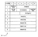
図8は、プローブパケット40の一実施例のブロック図を示す。異なった態様でプローブパケットを構成し、代替的な、同様の、または代用の情報を有する他の実施例も可能であり企図される。プローブパケット40は、図4に示すアドレスパケット32の1種である。図8に示すように、プローブパケット40はコマンドフィールド(図8におけるCMD[5:0])、ターゲットノードフィールド(図8におけるTgtNode[1:0]およびTgtNode[3:2])、ソースノードフィールド(図8におけるSrcNode[3:0])、ソースタグフィールド(図8におけるSrcTag[1:0]およびSrcTag[6:2])、データ移動フィールド(図8におけるDM)、ネクストステートフィールド(NextState[1:0])、およびアドレスフィールド(図8におけるビット時間4−8にわたるAddr[39:0])を含む。
【0038】
コマンドフィールドは符号化されてパケット40をプローブパケットとして識別する。たとえば、図7に示すProbe/SrcおよびProbe/Tgtに対する符号化を用い得る。一般的には、トランザクションのターゲットノードはプローブコマンドを生成して、トランザクションによって影響されるキャッシュブロックのコヒーレンシを維持する。開始されるトランザクションの種類に基づいて、プローブコマンドの組の中の1つがターゲットノードによって選択される。選択されたプローブコマンドは、プローブコマンドに対する応答のための受信ノードを識別する。多数の使用できる受信ノードのうちの1つに、柔軟にプローブ応答を経路制御することにより、(予め定められた受信ノードにプローブ応答を経路制御することとは対照的に)、コヒーレンシの維持は(たとえば、ノード間で送信されるパケットの数の観点から)効率的であって、正確な結果を導く態様で行なうことができる。
【0039】
たとえば、キャッシュブロックをトランザクションのソースノードに転送させるトランザクションは、プローブ応答(データを転送する応答を含む)をソースノードに向けることにより、コヒーレンシを維持し得る。ソースノードは、他のノード(プローブされたノード)の各々からの応答とターゲットノードからの応答とを待ち、次いでノード内に送信されたキャッシュブロックを確立し、かつターゲットノードに肯定応答パケットを送信してトランザクションを終了させる。トランザクションを終了させる前にプローブされたノードからのプローブ応答を待つことにより、ノードの各々は終了の前にそのトランザクションに対する正しいコヒーレンシ状態を確立し得る。一方、WrSizedトランザクション(キャッシュブロックに満たない更新をする)は、WrSizedコマンドと関連のデータとをターゲットノードに送信することにより開始される。ターゲットノードは、ターゲットノードのメモリにデータをコミットするために、ターゲットノードはソースノードの代わりにプローブ応答を受信し得る。特に、WrSizedトランザクションによって更新されたバイトを含むキャッシュブロックがプローブノード内でダーティであれば、ターゲットノードはプローブに応答してダーティなデータを受信し、そのデータをWrSizedコマンドに関連のデータとマージし得る。一旦プローブ応答が受取られると、書込動作によって命令されるコヒーレンシ状態はプローブされたノード内で確立され、書込データはメモリにコミットし得る。したがってこの実施例においては、2つの種類のプローブコマンドがサポートされ、どのノードがプローブ応答を受取るべきであるかをプローブされたノードに対して示す(たとえばソースまたはターゲットノード)。他の実施例は、所望により、付加的な受信ノードを示す付加的なプローブコマンドをサポートし得る。
【0040】
1つの例示的な実施例においては、ターゲットノード内のメモリコントローラは処理されるべき要求のキューからトランザクションを選択することができ、かつその選択に応答してプローブコマンドを生成し得る。プローブコマンドはコンピュータシステム内のプローブされたノードにブロードキャストされることができる。コマンドフィールドは、プローブ応答がターゲットノードまたはソースノードに経路制御されるべきかどうかを示す。たとえば、図7に示すテーブル38において例示するように、コマンドフィールドのビット0は受信ノードを示し得る(バイナリ0はソースノードを、バイナリ1はターゲットノードを示す)。ターゲットノードフィールドはトランザクションのターゲットノードを識別し、ソースノードフィールドはトランザクションのソースノードを識別する。プローブコマンドもまたターゲットノード内のキャッシュにブロードキャストされ、ターゲットノードはプローブ応答を提供し得ることに留意されたい。言い換えると、ターゲットノードもまたプローブされたノードであり得る。
【0041】
さらに、データ移動フィールド(一実施例においては、たとえば1ビット)を用いて、プローブされたノード内でキャッシュブロックがダーティであった場合にプローブに応答してデータが返されるべきかどうかを表示し得る。データ移動フィールドがいずれの移動も示さなければ(たとえばクリアな状態)、ダーティデータを持つノードはプローブ応答を宛先指定された受信ノードに戻すが、ダーティデータを受信ノードに送信しない。データ移動フィールドが移動を示せば(たとえばセットされた状態)、ダーティデータを持つノードは、ダーティデータを含む読出応答をソースノードに返す。ネクストステートフィールドは、(プローブされたノードがキャッシュブロックのコピーをストアしている場合)プローブされたノードにおいてキャッシュブロックの次の状態がどうなるかを示す。一実施例においては、ネクストフィールドの符号化は以下のテーブル1に示すとおりである。
【0042】
一実施例によると、以下のテーブル2は例示的なトランザクションタイプと対応のプローブコマンドを示す。
【0043】
【表1】
一般的には、「プローブ」または「プローブコマンド」という用語は、プローブノードに対する要求を指し、これによりプローブによって(たとえばアドレスフィールドを介して)定義されるキャッシュブロックがプローブされたノードによってストアされているかどうか判断し、かつプローブされたノードからの所望の応答を示す。応答は、キャッシュブロックに対する異なったコヒーレンシ状態を確立すること、および/またはキャッシュブロックを受信ノードに転送することを含む。プローブされたノードは「プローブ応答」を用いて応答するが、これは所望のコヒーレンシ状態変化が行なわれたことを受信ノードに肯定応答する。プローブ応答は、プローブされたノードがダーティデータをストアしていた場合、データをも含み得る。
【0045】
図9は、プローブ応答パケット42の一実施例のブロック図を示す。応答パケットを異なった態様で構成し、代替的な、同様の、または代用の情報を有する他の実施例も可能であり企図される。プローブ応答パケット42は、図5に示す応答パケット34の1種である。図8に示すプローブパケットと同様に、プローブ応答パケット42はコマンドフィールド(CMD[5:0])、ソースノードフィールド(SrcNode[3:0])、およびソースタグフィールド(SrcTag[1:0]およびSrcTag[6:2])を含み得る。さらに、プローブ応答パケット42は、応答ノードフィールド(図9におけるRespNode[3:2]およびRespNode[1:0])およびヒット表示(図9におけるHit)を含み得る。
【0046】
プローブされたノードは、プローブパケット40で受信されたアドレスによって識別されたキャッシュブロックに対して、そのキャッシュ内を探索する。キャッシュブロックのコピーを見出すと、プローブされたノードはネクストステートフィールドにより規定されていることにしたがってキャッシュブロックの状態を変化させる。さらに、キャッシュがキャッシュブロックのダーティコピーをストアしており、かつプローブパケット40のデータ移動フィールドがキャッシュブロックが転送されるべきであることを示すと、プローブされたノードはキャッシュからダーティデータを読出す。
【0047】
プローブされたノードは、プローブ応答パケット42を以下の場合において指定された受信ノードに経路制御する。すなわち、(i)ダーティデータがない場合、または(ii)ダーティデータおよびデータ移動フィールドがいずれの移動も示さない場合。この実施例においてより特定的には、プローブされたノードはプローブパケット40のターゲットノードフィールド(指定された受信ノードがターゲットノードである場合)か、またはプローブパケット40のソースノードフィールド(指定された受信ノードがソースノードである場合)のいずれかを読出し、結果として生じるノードIDをプローブ応答パケット42の応答ノードフィールドにストアする。さらに、ヒット表示を用いて、プローブノードがキャッシュブロックのコピーを保持しているかどうかを示す。たとえば、ヒット表示は、セットされている場合に、プローブされたノードがキャッシュブロックのコピーを保持していることを示し、そしてクリアされている場合に、プローブされたノードがキャッシュブロックのコピーを保持していないことを示すビットを含み得る。ヒットビットは、以下の場合にクリアされている。すなわち、(i)プローブされたノード内のキャッシュにおいてキャッシュブロックのコピーが見出されなかった場合、または(ii)プローブされたノードにおけるキャッシュ内でキャッシュブロックのコピーが見出されたが、プローブコマンドに応答して無効化されていた場合、である。
【0048】
図7のテーブル38に示す一実施例においては、プローブ応答パケット42のコマンドフィールドはProbRespを示すことができ、さらにプローブ応答がProbe/Srcコマンドへの応答であるか、またはProbe/Tgtコマンドへの応答であるかをさらに示すことができる。より特定的には、コマンドフィールドのビット0はクリアされてプローブ応答がProbe/Srcコマンドへの応答であることを示し、セットされてプローブ応がはProbe/Tgtコマンドへの応答であることを示す。この表示は受信ノードによって用いられて、プローブ応答が受信ノード内のメモリコントローラに経路制御されるべきか(ビット0がセットされている場合)、または受信ノード内のキャッシュに対するフィル受信ロジックに対して経路制御されるべきか(ビット0がクリアされている場合)を判断し得る。
【0049】
図10は、読出応答パケット44の一実施例のブロック図を示す。読出応答パケットを異なった態様で構成し、代替的な、同様の、または代用の情報を有する他の実施例も可能であり企図される。応答パケット44は図5に示す応答パケット34の1種である。図9に示すプローブ応答パケットと同様に、読出応答パケット44は、コマンドフィールド(CMD[5:0])、ソースノードフィールド(SrcNode[3:0])、ソースタグフィールド(SrcTag[1:0]およびSrcTag[6:2])、および応答ノードフィールド(RespNode[3:2]およびRespNode[1:0])を含む。さらに、読出応答パケット44は、カウントフィールド(図10におけるCount)、タイプフィールド(図10におけるType)およびプローブフィールド(図10におけるPrb)を含む。
【0050】
データ移動が要求されることを示すプローブコマンドに対してダーティデータのヒットを検出した、プローブされたノードは、読出パケット44を用いてプローブ応答およびダーティデータを送信し得る。カウントフィールドを用いて送信されるデータの量を示し、タイプフィールドはカウントがバイトまたはクワッドワード(8バイト)で測定されるかを示す。プローブに対して応答するキャッシュブロック転送に対しては、カウントフィールドは8(バイナリ「111」として符号化される)を示し、タイプフィールドはクワッドワード(たとえば、一実施例においてはタイプフィールドにおいてセットされたビット)を示す。プローブフィールドを用いて、読出応答パケット44がターゲットノードまたはプローブされたノードのいずれから送信されているかを示す。たとえば、プローブフィールドは、セットされている場合に読出応答パケット44がプローブされたノードから転送されたことを示し、クリアされている場合に読出応答パケット44がターゲットノードから送信されたことを示す、ビットを含み得る。したがって、プローブされたノードは読出応答パケット44を用いる場合にプローブビットをセットする。
【0051】
読出応答パケット44は、データパケットが後に続くことを示すパケットタイプである。したがって、プローブされたノードは読出応答パケット44の後にデータパケットでキャッシュブロックを送信する。プローブされたノードは、読出応答パケット44を、上述のようにプローブ読出パケット42を経路制御するのと同様の態様で経路制御する(たとえば、プローブされたノードは(指定された受信ノードがターゲットノードであれば)プローブパケット40のターゲットノードフィールドを読出すか、または(指定された受信ノードがソースノードであれば)プローブパケット40のソースノードフィールドを読出し、結果として生じるノードIDを読出応答パケット44の応答ノードフィールドにストアする)。
【0052】
図7のテーブル38において示される一実施例においては、読出応答パケット44のコマンドフィールドはRdResponseを示すことができ、さらに読出応答がProbe/Srcコマンドへの応答であるか、またはProbe/Tgtコマンドへの応答であるかを示し得る。より特定的には、コマンドフィールドのビット0はクリアされて読出応答がProbe/Srcコマンドへの応答であることを示し、セットされて読出応答がProbe/Tgtコマンドへの応答であることを示す。この表示を受信ノードによって用いて、読出応答が受信ノード内のメモリコントローラに経路制御されるべきか(ビット0がセットされている場合)、または受信ノード内のキャッシュに対するフィル受信ロジックに経路制御されるべきか(ビット0がクリアされている場合)を判断し得る。
【0053】
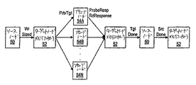
図11は、例示的な読出ブロックトランザクションに対応する1組のノードの間のパケットフローを示す図である。ソースノード50、ターゲットノードメモリコントローラ52、および1組のプローブされたノード54A−54Nを示す。図11にはパケットの(時系列での)順序を左から右に示す。言い換えると、RdBlkパケットはソースノード50からターゲットノードメモリコントローラ52に送信され、その後でターゲットノードメモリコントローラ52はProbe/Srcパケットをプローブノード54A−54Nに送り、以下も同様である。パケットの時間順序を示すために、図11ではソースノード50およびターゲットメモリコントローラ52を2箇所に示す。同様に、図12および図13では特定のブロックを1箇所以上に示す。ソースノード50、ターゲットノードメモリコントローラ52を含むターゲットノード、プローブされたノード54A−54Nの各々は、図1に示す処理ノード12A−12Dと同様の処理ノードを含み得る。
【0054】
ソースノード50はRdBlkパケットをターゲットノードメモリコントローラ52に送信して、読出ブロックトランザクションを開始する。次いでターゲットノードメモリコントローラ52は処理されるべきRdBlkパケットを選択する。ターゲットノードメモリコントローラ52はProbe/Srcパケットを生成し、パケットをプローブされたノード54A−54Nにブロードキャストする。さらに、ターゲットノードメモリコントローラ52は、ターゲットノードメモリコントローラ52が結合されているメモリ14A−14Dからの読出を開始する。メモリ14A−14Dからの読出が完了すると、ターゲットノードメモリコントローラ52はデータを含むRdResponseパケットを生成し、パケットをソースノード50に送信する。
【0055】
プローブされたノード54A−54Nの各々はそのキャッシュ内を探索して、RdBlkパケットによって読出されたキャッシュブロックがその中にストアされているかどうか判断する。ヒットが検出されると、対応するプローブされたノード54A−54Nは、ターゲットノードメモリコントローラ52から受取ったプローブパケット内のネクストステートフィールドに従ってキャッシュブロックの状態を更新する。さらに、プローブされたノード54A−54Nの各々は(Probe/Srcパケットが既に受信されているために)、ProbeRespパケットをソースノード50に経路制御する。この例においては、いずれのプローブされたノード54A−54Nもキャッシュブロックのダーティコピーをストアしていない。
【0056】
ソースノード50は、プローブされたノード54A−54NからのProbeRespパケットおよびターゲットメモリコントローラ52からのRdResponseパケットを待機する。一旦これらのパケットが受取られると、ソースノード50はSrcDoneパケットをターゲットメモリコントローラ52に送信し、トランザクションを終了する。
【0057】
次いで図12は、第2の例示的な読出ブロックトランザクションを例示する図を示す。ソースノード50、ターゲットメモリコントローラ52、プローブされたノード54A−54Nが示される。ソースノード50、ターゲットメモリコントローラ52を含むターゲットノード、およびプローブされたノード54A−54Nの各々は、図1に示す処理ノード12A−12Dと同様の処理ノードを含み得る。
【0058】
図11に示す例と同様に、ソースノード50はRdBlkパケットをターゲットメモリコントローラ52に送信する。ターゲットノードメモリコントローラ52はProbe/Srcパケットをプローブされたノード54A−54Nに送信し、かつRdResponseパケットをソースノード50に送信し得る。
【0059】
図12の例においては、プローブされたノード54Aは読出ブロックトランザクションによってアクセスされたキャッシュブロックに対してダーティデータを検出する。したがって、プローブされたノード54Aは(Probe/Srcコマンドにより命令されて)ソースノード50に、RdResponseパケットとプローブされたノード54Aの内部キャッシュから読出されたダーティキャッシュブロックとを送信する。したがって、一実施例においては、プローブされたノード54AはMemCancelパケットをターゲットノードメモリコントローラ52に送信し得る。ターゲットノードメモリコントローラ52がRdResponseパケットをソースノード50に送信する前に、MemCancelパケットがターゲットノードメモリコントローラ52に到達すると、ターゲットノードメモリコントローラ52はRdResponseパケットを送信しない。よって、ターゲットノードメモリコントローラ52からソースノード50への「RdResponse」と表示された線は、その選択的な性質を示すために点線で表わされる。MemCancelメッセージに応答して、ターゲットノードメモリコントローラ52はTgtDoneパケットをソースノード50に送信する。
【0060】
プローブされたノード54B−54Nは、この実施例においてはダーティデータを検出せず、よってProbeRespパケットをソースノード50に経路制御する。一旦ソースノード50がTgtDone、RdResponse、およびProbeRespパケットを受取ると、ソースノード50はSrcDoneパケットをターゲットメモリコントローラ52に送信して読出ブロックトランザクションを終了させる。
【0061】
図13は、例示的なサイズ指定された書込トランザクションを示す図である。ソースノード50、ターゲットノードメモリコントローラ52、およびプローブされたノード54A−54Nを示す。ソースノード50、ターゲットノードメモリコントローラ52を含むターゲットノード、およびプローブされたノード54A−54Nの各々は、図1に示す処理ノード12A−12Dと同様の処理ノードを含み得る。
【0062】
ソースノード50は、WrSizedパケットおよび書込まれるべきデータをターゲットノードメモリコントローラ52に送信することにより、サイズ指定された書込トランザクションを開始する。サイズ指定された書込トランザクションは、キャッシュブロックの一部を更新するが、キャッシュブロックの残りの部分は更新しないために、ターゲットノードメモリコントローラ52はプローブされたノード54A−54Nから(もし存在すれば)ダーティキャッシュブロックを収集する。さらに、キャッシュブロックのクリーンなコピーはプローブされたノード54A−54Nにおいて無効化され、コヒーレンシを維持する。ターゲットメモリコントローラ52は、処理されるべきサイズ指定された書込トランザクションを選択する際に、Probe/Tgtパケットをプローブされたノード54A−54Nに送信する。プローブされたノード54A−54Nは、(Probe/Tgtパケットが受取られているために)ターゲットノードメモリコントローラ54に、(いずれのダーティデータも検出されなければ)ProbeRespパケットか、または(ダーティデータが検出されると)RdResponseパケットのいずれかを返す。一旦ターゲットノードメモリコントローラ52が、プローブされたノード54A−54Nからの応答を受取ると、ターゲットノードメモリコントローラ52はTgtDoneパケットをソースノード50に送信し、これはサイズ指定された書込トランザクションを終了させるSrcDoneパケットで応答する。
【0063】
ターゲットノードメモリコントローラ52が、プローブされたノード54A−54Nのうちの1つからダーティなキャッシュブロックを受取ると、ターゲットノードメモリコントローラ52は、ダーティキャッシュブロックとWrSizedデータパケット内のソースノード50によって提供されたバイトとのマージを実行する。マージを実行するためのいかなる好適な機構をも用い得る。たとえば、ターゲットノードメモリコントローラ52はデータをマージし、単一ブロック書込を行なってメモリを更新してもよい。これに代えて、ダーティブロックが第1にメモリに書込まれ、次いでソースノード50によって提供されたバイトの書込が続いてもよい。
【0064】
この説明は、ノード間で通信されるパケットについて記載する一方で、コマンド、応答および他のメッセージを送信するためのいかなる好適な機構をも用い得ることに留意されたい。
【0065】
図14は、処理のためのトランザクションの選択に応答する、メモリコントローラ16A−16Dの一実施例の一部の動作を例示するフローチャートを示す。特に、プローブを生成するメモリコントローラ16A−16Dの部分が示される。他の実施例も可能であり企図される。図14において、理解を容易にするためにステップを特定の順序に従って示すが、いかなる好適な順序をも用い得る。さらに、ステップはデザイン選択によって所望のように、メモリコントローラ16A−16D内で並列ハードウェアを用いてステップを並行して行なってもよい。
【0066】
メモリコントローラは、選択されたトランザクションがWrSizedトランザクションであるかどうか判断する(判断ブロック60)。もし選択されたトランザクションがWrSizedトランザクションであれば、メモリコントローラはProbe/Tgtパケットをプローブノードの各々に送信する(ステップ62)。そうでなければ、メモリコントローラは選択されたトランザクションがVicBlkまたはCleanVicBlkトランザクションであるかどうか判断する(判断ブロック64)。選択されたトランザクションがVicBlkまたはCleanVicBlkトランザクションであれば、プローブパケットは生成されない。しかしながら、選択されたトランザクションがWrSized、VicBlk、またはCleanVicBlkでなければ、Probe/Srcパケットはプローブされたノードに送信される(ステップ66)。
【0067】
図15は、プローブパケットに応答するプローブされたノードの一実施例の動作を示すフローチャートである。他の実施例も可能であり企図される。図15において、理解を容易にするためにステップを特定の順序に従って示すが、いかなる好適な順序をも用い得る。さらに、設計選択によって所望のように、プローブされたノード内で並列ハードウェアを用いてステップを並行して行なってもよい。
【0068】
プローブされたノードはそのキャッシュを探索して、プローブによって表示されたキャッシュブロックがその中にストアされているかどうか判断し、もしキャッシュブロックが見出されればその状態を判断する。キャッシュブロックがダーティな状態で見出されると(判断ブロック70)、プローブされたノードはRdResponseパケットを生成する。プローブされたノードはRdResponseパケットの後にキャッシュからダーティデータを読出して、データパケットとして送信する(ステップ72)。一方で、キャッシュブロックが見出されないか、またはダーティな状態になければ、プローブされたノードはProbeRespパケットを生成する(ステップ74)。さらに、キャッシュブロックの状態はプローブパケットのネクストステートフィールドに特定されるように更新される。
【0069】
プローブされたノードは受取ったプローブパケットを調べる(判断ブロック76)。プローブパケットがProbe/Srcパケットであれば、プローブされたノードは上で生成された応答を、Probe/Srcパケットに表示されるソースノードに経路制御する(ステップ78)。言い換えると、プローブされたノードは応答パケット内のRespNodeフィールドを、Probe/SrcパケットのSrcNodeフィールド内の値にセットする。一方、プローブパケットがProbe/Tgtパケットであれば、プローブされたノードは上で生成された応答を、Probe/Tgtパケットに表示されるターゲットノードに経路制御する(ステップ80)。言い換えると、プローブされたノードは応答パケット内のRespNodeフィールドを、Probe/TgtパケットのTgtNodeフィールド内の値にセットする。
【0070】
図16は、例示的な処理ノード12Aの一実施例のブロック図を示す。他の実施例も可能であり企図される。図16の実施例においては、処理ノード12Aはインターフェイスロジック18A、18B、18Cおよびメモリコントローラ16Aを含む。さらに、処理ノード12Aは、プロセッサコア92、キャッシュ90、コヒーレンシ管理ロジック98、および選択により第2のプロセッサコア96および第2のキャッシュ94を含み得る。インターフェイスロジック18A−18Cは互いに結合され、さらにコヒーレンシ管理ロジック98に結合される。プロセッサコア92および96は、それぞれキャッシュ90および94に結合される。キャッシュ90および94は、コヒーレンシ管理ロジック98に結合される。コヒーレンシ管理ロジック98はメモリコントローラ16Aに結合される。
【0071】
一般的に、コヒーレンシ管理ロジック98は、メモリコントローラ16Aによって処理のために選択されたトランザクションに応答してプローブコマンドを生成し、かつ処理ノード12Aによって受取られるプローブコマンドに応答するよう構成される。コヒーレンシ管理ロジック98は、処理のために選択されたトランザクションのタイプに依存して、Probe/SrcコマンドまたはProbe/Tgtコマンドのいずれかをブロードキャストする。さらに、コヒーレンシ管理ロジック98は、受取ったプローブコマンドによって特定されるキャッシュブロックに対してキャッシュ90および94を探索し、適切なプローブ応答を生成する。さらに、Probe/Tgtコマンドを生成する場合には、コヒーレンシ管理ロジック98は、Probe/Tgtコマンドに応答して返されたプローブ応答を収集し得る。キャッシュ90および94は、処理ノード12A内で開始された読出要求からのデータの受取を管理するフィルロジックを含むか、またはコヒーレンシ管理ロジック98内にフィルロジックが含まれてもよい。コヒーレンシ管理ロジック98はさらに、メモリコントローラ16Aに対する非コヒーレント要求を経路制御するよう構成されてもよい。一実施例においては、プロセッサ92とプロセッサ96とは、キャッシュ90、キャッシュ94、およびコヒーレンシ管理ロジック98をバイパスして、特定のキャッシュ不可および/または非コヒーレントメモリ要求に対して直接メモリコントローラ16Aにアクセスし得る。
【0072】
キャッシュ90および94は、データのキャッシュブロックをストアするよう構成された高速キャッシュメモリを含む。キャッシュ90および94は、それぞれのプロセッサコア92および96内に統合されてもよい。これに代えて、キャッシュ90および94は、所望のようにプロセッサコア92および96に、バックサイドキャッシュ構成またはインライン構成で結合されてもよい。さらに、キャッシュ90および94はキャッシュ階層構造として実現化されてもよい。プロセッサコア92および96に(階層内で)より近いキャッシュは、所望であればプロセッサコア92および96に統合されてもよい。
【0073】
プロセッサコア92および96は、予め定められた命令セットに従って命令を実行するための回路を含む。たとえば、x86命令セットアーキテクチャを選択し得る。これに代えて、Alpha、PowerPC、または他のいかなる命令セットアーキテクチャを選択してもよい。一般的に、プロセッサコアはデータおよび命令のためにキャッシュにアクセスする。キャッシュミスが検出されると、読出要求が生成され、ミスの発生したキャッシュブロックがマッピングされているノード内のメモリコントローラに送信される。
【0074】
分散メモリシステムを用いて、コンピュータシステム10の特定の実施例を説明してきたが、分散メモリシステムを用いない実施例も、ここで説明した柔軟なプローブ/プローブ応答経路制御を用い得ることに留意されたい。そのような実施例が企図される。
【0075】
上の開示を完全に理解すると、当業者においてはいくつもの変更および変形が明らかとなるであろう。前掲の特許請求の範囲がすべてのそのような変更および変形を包含することが理解されることを意図する。
【0076】
【産業上の用途】
この発明は一般的にコンピュータシステムに適用可能である。
【図面の簡単な説明】
【図1】 コンピュータシステムの一実施例のブロック図である。
【図2】 図1に示す1対の処理ノードの間の相互接続の一実施例を強調した、ブロック図である。
【図3】 情報パケットの一実施例のブロック図である。
【図4】 アドレスパケットの一実施例のブロック図である。
【図5】 応答パケットの一実施例のブロック図である。
【図6】 データパケットの一実施例のブロック図である。
【図7】 コンピュータシステムの一実施例によって用い得る、例示的なパケットタイプを示すテーブルである。
【図8】 プローブパケットの一実施例のブロック図である。
【図9】 プローブ応答パケットの一実施例のブロック図である。
【図10】 読出応答パケットの一実施例のブロック図である。
【図11】 読出ブロックトランザクションに対応するパケットの例示的なフローを示す図である。
【図12】 読出ブロックトランザクションに対応するパケットの第2の例示的なフローを示す図である。
【図13】 サイズ指定された書込トランザクションに対応するパケットの例示的なフローを示す図である。
【図14】 メモリコントローラの一実施例の動作を示すフローチャートの図である。
【図15】 プローブパケットを受取る処理ノードの一実施例の動作を示すフローチャートの図である。
【図16】 処理ノードの一実施例のブロック図である。[0001]
BACKGROUND OF THE INVENTION
1.Technical field
The present invention relates generally to computer systems, and more specifically to a message communication scheme for achieving a multiprocessing computing environment.
[0002]
2.Background of related technical fields
“Efficient and Scalable Cache Coherence Schemes for Shared Memory Hypercube Microprocessors for Shared Memory Hypercube Microprocessors” by Kumar A et al., Proceedings of the Supercomputing Conference, US Loss Alamitos, IEEE, Vol. Conf. 7. 1994, pp. 498-507 includes a computer system having the characteristics described in the preamble of
EP-A-0 817 076 discloses a multiprocessing computer system that uses local and global address spaces and multiple access modes. A processor within a node may initiate a transaction requesting inter-node communication. When a request is sent from the requesting node to the home node, the home node sends a read and / or invalidation request to any of the subordinate nodes that have a cached copy of the requested data. The system implements a global coherency protocol for maintaining cache coherency.
In general, personal computers (PCs) and other types of computer systems have been designed around shared bus systems to access memory. One or more processors and one or more input / output (I / O) devices are coupled to the memory via a shared bus. While I / O devices may be coupled to the shared bus via an I / O bridge that manages the transfer of information between the shared bus and the I / O device, the processor is typically directly shared Coupled to a bus or coupled to a shared bus through a cache hierarchy.
[0003]
Unfortunately, the shared bus system has several drawbacks. For example, because a large number of devices are mounted on a shared bus, the bus is typically operated at a relatively low frequency. Multiple attachments provide a capacitive and high load on the devices that drive signals on the bus, and multiple attachment points provide a transmission line model for relatively complex high frequencies. Therefore, the frequency is kept low and the bandwidth available on the shared bus is also relatively low. Low bandwidth can be a barrier to mounting additional devices on a shared bus, because performance can be limited by available bandwidth.
[0004]
Another drawback of the shared bus system is the lack of scalability for more devices. As mentioned above, the bandwidth is fixed (and can be reduced if the operational frequency of the bus is reduced by the addition of additional devices). Once the bandwidth requirements of a device attached to the bus (directly or indirectly) exceeds the available bandwidth of the bus, the device can often stall when attempting to access the bus. Overall performance will be reduced.
[0005]
One or several of the above problems may be addressed using a distributed memory system. A computer system using a distributed memory system includes a plurality of nodes. Two or more nodes are connected to the memory, and the nodes are interconnected using any suitable interconnect. For example, each of the nodes can be connected to each other using a dedicated line. Alternatively, each of the nodes is connected to a fixed number of other nodes, and the transaction is not directly connected to the first node from the first node via one or more intermediate nodes. May be routed to other nodes. Memory address space is allocated across the memory of each node.
[0006]
A node may further include one or more processors. The processor typically includes a cache that stores a cache block of data read from the memory. In addition, a node may include one or more caches external to the processor. A mechanism for maintaining coherency within a node is desired because the processor and / or node may store cache blocks accessed from other nodes.
[0007]
DISCLOSURE OF THE INVENTION
The problems outlined above are mostly solved by the computer system described herein. The computer system can include multiple processing nodes, one or more of which can be coupled to separate memories that can form a distributed memory system. The processing node can include a cache, and the computer system can maintain coherency between the cache and the distributed memory system. In particular, the computer system can implement a flexible probe command / response path control scheme.
[0008]
In one embodiment, the scheme uses an indication in the probe command that identifies the receiving node that receives the probe response. In general, a probe command is a request to a node to determine whether a cache block is stored in the node, and should be performed by the node when the cache block is stored in the node. It is an operation display. The probe response indicates that an action has been taken and may include sending data if the cache block has been modified by the node. Maintaining coherency in a relatively efficient manner (eg, processing nodes with a minimum number of packets) by providing flexibility in routing probe responses to different receiving nodes depending on the commands sent To ensure that coherency is still maintained.
[0009]
For example, it may include a probe command that indicates that the target or source of the transaction should receive a probe response corresponding to the transaction. The probe command may identify the source of the transaction as the receiving node for the read transaction (which causes the dirty data to be passed from the node storing the dirty data to the source node). On the other hand, for a write transaction (data is updated in memory at the target node of the transaction), the probe command may identify the target of the transaction as the receiving node. In this way, the target can determine when to commit write data to memory and receive any dirty data to be merged with the write data.
[0010]
In general, a computer system is contemplated. The computer system can include a first processing node and a second processing node. The first processing node may be configured to initiate a transaction by sending a request. The second processing node may be coupled to receive a request from the first processing node and configured to generate a probe in response to the request. The probe may include an indication that specifies a receiving node for receiving a response to the probe. Further, the second processing node may be configured to generate a display in response to the type of transaction.
[0011]
A method for maintaining coherency within a computer system is also contemplated. A request from the source node is sent to the target node. A probe is generated in the target node in response to the request. Via a display in the probe, the receiving node for the response to the probe is specified. The probe response to the probe is routed to the receiving node.
[0012]
Other objects and advantages of the present invention will become more apparent upon reading the following detailed description and upon reference to the accompanying drawings.
[0013]
While the invention addresses various modifications and alternative forms, specific embodiments thereof are shown by way of example in the drawings and are described in detail below. However, the drawings and detailed description are not intended to limit the disclosed invention to a particular form, but on the contrary, all modifications, equivalents, and alternatives are defined in the appended claims. It is intended to be within the scope of this invention.
[0014]
DETAILED DESCRIPTION OF THE INVENTION
Exemplary Computer System Embodiment
FIG. 1 illustrates one embodiment of a
[0015]
[0016]
[0017]
Memory 14A-14D may include any suitable memory device. For example, the memories 14A-14D may include one or more RAMBUS DRAM (RDRAM), synchronous DRAM (SDRAM), static RAM, and the like. The address space of
[0018]
In general, the
[0019]
Next, FIG. 2 shows a block diagram of
[0020]
The clock line transmits a clock signal indicating sample points for the control line and the control / address / data bus. In one particular embodiment, data / control bits are transmitted on each of the edges of the clock signal (ie, rising and falling edges). Thus, every clock cycle, two data bits can be transmitted per line. The time used to transmit one bit per line is referred to herein as “bit time”. The embodiment described above includes two bit times per clock cycle. A packet may be transmitted in more than one bit time. Depending on the width of the control / address / data bus, multiple clock lines may be used. For example, two clock lines may be used for a 32-bit control / address / data bus (one clock line is referenced in half of the control / address / data bus and the other half of the control / address / data bus and control Line refers to the other clock line). In general, a “packet” is a communication between two
[0021]
The control line indicates whether the data sent to the control / address / data bus is a bit time control packet or a bit time data packet. The control line is asserted to indicate a control packet and deasserted to indicate a data packet. A control packet indicates that a data packet follows. The data packet may immediately follow the corresponding control packet. In one embodiment, other control packets may interrupt the transmission of data packets. Such an interrupt could be done by asserting the control line for several bit times during the transmission of the data packet and sending a bit time control packet while the control line is asserted. is there. A control packet that interrupts a data packet may not indicate that the data packet follows.
[0022]
The control / address / data bus includes a set of lines for transmitting data / control bits. In one embodiment, the control / address / data bus may include 8, 16, or 32 lines. Each processing node or I / O bridge may use any of the number of lines supported according to design choices. Other embodiments may support other sizes of control / address / data buses as desired.
[0023]
According to one embodiment, command / address / data bus lines and clock lines may carry inverted data (ie,
[0024]
FIGS. 3-6 illustrate exemplary packets used in accordance with one embodiment of the
[0025]
FIG. 3 shows an information packet (info packet) 30.
[0026]
FIG. 4 shows an address packet (address packet) 32.
[0027]
FIG. 5 shows a response packet (response packet) 34. The
[0028]
FIG. 6 shows a data packet (data packet) 36.
[0029]
3 to 6 show packets for an 8-bit link. Packets for 16 and 32 bit links may be formed by concatenating consecutive bit times as shown in FIGS. For example,
[0030]
[Expression 1]
FIG. 7 shows a table 38 showing commands used by one exemplary embodiment of links in
[0032]
A read transaction is initiated using one of the commands ReadSized, RdBlk, RdBlkS or RdBlkMod. ReadSized, which is a size-specified read command, is used for non-cacheable read or for reading data other than a cache block having a suitable size. The amount of data to be read is encoded in a ReadSized command packet. For reading the cache block, the RdBlk command can be used except in the following cases. (I) When a writable copy of the cache block is desired. In this case, the RdBlkMod command can be used. Or (ii) A copy of the cache block is desired, but the block is not intended to be changed. In this case, the RdBlkS command can be used. The RdBlkS command can be used to make certain types of coherent schemes (eg, directory-based coherent schemes) more efficient. In general, an appropriate read command is sent from the source to initiate a read transaction to a target node having a memory corresponding to the cache block. The memory controller in the target node sends Probe / Src commands to other nodes in the system to change the state of the cache blocks in these nodes, and to the node that contains the updated copy of the cache block Coherency is maintained by having the cache block sent to the source node. Each node that receives the Probe / Src command transmits a ProbeResp packet to the source node. If the probed node has an updated copy of read data (ie dirty data), it sends an RdResponse packet and dirty data. A node sending dirty data may also send a MemCancel packet to the target node in an attempt to cancel transmission of the requested read data by the target node. Further, the memory controller in the target node transmits the requested read data using the RdResponse packet and the data in the subsequent data packet. If the source node receives an RdResponse packet from the probed node, the read data is used. Otherwise, data from the target node is used. Once the probe response and each of the read data are received at the source node, the source node sends a SrcDone response packet to the target node as an acknowledgment of the end of the transaction.
[0033]
A write transaction is initiated using a WrSized or VicBlk command, followed by the associated data packet. The WrSized command is used for non-cacheable writing or writing of data in a cache block whose size does not match. In order to maintain coherency for the WrSized command, the memory controller in the target node sends a Probe / Tgt command to each of the other nodes in the system. In response to the Probe / Tgt command, each probed node transmits a ProbeResp packet to the target node. If the probed node stores dirty data, the probed node responds with an RdResponse packet and dirty data. In this way, the cache block updated by the WrSized command is returned to the memory controller and merged with the data provided by the WrSized command. When the memory controller receives a probe response from each of the probed nodes, it sends a TgtDone packet to the source node to provide an acknowledgment of the end of the transaction. The source node responds with an SrcDone response packet.
[0034]
A victim cache block that has been modified by a node and replaced with a cache in the node is returned to memory using the VicBlk command. No probe is required for the VicBlk command. Thus, when the target memory controller is ready to commit victim block data to memory, the target memory controller sends a TgtDone packet to the source node of the victim block. The source node indicates an SrcDone packet indicating that the data should be committed, or indicates that the data was invalidated between sending a VicBlk command and receiving a TgtDone packet (eg in response to an intervening probe) Respond with one of the MemCancel packets.
[0035]
In order to obtain write permission to the unwritable cache block stored at the source node, the source node may send a ChangetoDirty packet. A transaction initiated by a ChangetoDirty command can behave similarly to a read, except that the target node does not return data. If the source node intends to update the entire cache block, the ValidateBlk command can be used to obtain permission to write to a cache block that is not stored by the source node. For such transactions, no data is transferred to the source node, but otherwise it behaves like a read transaction.
[0036]
InterruptBroadcast, InterruptTarget, and IntrResponse packets can be used to broadcast interrupts, send interrupts to specific target nodes, and respond to interrupts. The CleanVicBlk command can be used to tell that a clean victim block has been discarded from a node (eg, for a directory based coherent scheme). The TgtStart command is used by the target to indicate that a transaction has started (eg, for later transaction ordering). Send error indication using error command.
[0037]
Probe / probe response path control
FIG. 8 shows a block diagram of an embodiment of the
[0038]
The command field is encoded to identify
[0039]
For example, a transaction that causes a cache block to be transferred to the source node of the transaction may maintain coherency by directing a probe response (including a response that transfers data) to the source node. The source node waits for a response from each of the other nodes (probed nodes) and the response from the target node, then establishes the cache block sent in the node and sends an acknowledgment packet to the target node To end the transaction. By waiting for a probe response from the probed node before ending the transaction, each of the nodes can establish the correct coherency state for that transaction before ending. On the other hand, a WrSized transaction (updating less than a cache block) is started by sending a WrSized command and related data to the target node. The target node may receive a probe response on behalf of the source node in order for the target node to commit data to the target node's memory. In particular, if the cache block containing bytes updated by a WrSized transaction is dirty in the probe node, the target node receives dirty data in response to the probe and merges that data with the data associated with the WrSized command. obtain. Once the probe response is received, the coherency state dictated by the write operation is established within the probed node and the write data can be committed to memory. Thus, in this example, two types of probe commands are supported, indicating to the probed node which node should receive the probe response (eg, source or target node). Other embodiments may support additional probe commands indicating additional receiving nodes as desired.
[0040]
In one exemplary embodiment, the memory controller in the target node can select a transaction from a queue of requests to be processed and can generate a probe command in response to the selection. Probe commands can be broadcast to probed nodes in a computer system. The command field indicates whether the probe response should be routed to the target node or source node. For example, as illustrated in the table 38 shown in FIG. 7,
[0041]
In addition, a data movement field (in one embodiment, for example, 1 bit) is used to indicate whether data should be returned in response to the probe if the cache block is dirty within the probed node. obtain. If the data movement field does not indicate any movement (eg, clear), the node with dirty data returns a probe response to the destination receiving node but does not send dirty data to the receiving node. If the data movement field indicates movement (eg, set), the node with dirty data returns a read response containing dirty data to the source node. The next state field indicates what happens to the next state of the cache block at the probed node (if the probed node stores a copy of the cache block). In one embodiment, the encoding of the next field is as shown in Table 1 below.
[0042]
According to one embodiment, Table 2 below shows exemplary transaction types and corresponding probe commands.
[0043]
[Table 1]
In general, the term “probe” or “probe command” refers to a request to a probe node so that the cache block defined by the probe (eg, via an address field) is stored by the probed node. And indicates the desired response from the probed node. The response includes establishing a different coherency state for the cache block and / or transferring the cache block to the receiving node. The probed node responds with a “probe response”, which acknowledges the receiving node that the desired coherency state change has occurred. The probe response may also include data if the probed node has stored dirty data.
[0045]
FIG. 9 shows a block diagram of an embodiment of the
[0046]
The probed node searches the cache for the cache block identified by the address received in the
[0047]
The probed node routes the
[0048]
In one embodiment shown in the table 38 of FIG. 7, the command field of the
[0049]
FIG. 10 shows a block diagram of an embodiment of the
[0050]
A probed node that has detected a dirty data hit for a probe command indicating that data movement is required may send a probe response and dirty data using
[0051]
The
[0052]
In one embodiment shown in the table 38 of FIG. 7, the command field of the
[0053]
FIG. 11 is a diagram illustrating packet flow between a set of nodes corresponding to an exemplary read block transaction. A
[0054]
[0055]
Each of the probed
[0056]
[0057]
FIG. 12 then shows a diagram illustrating a second exemplary read block transaction.
[0058]
Similar to the example shown in FIG. 11, the
[0059]
In the example of FIG. 12, the probed
[0060]
Probed
[0061]
FIG. 13 is a diagram illustrating an exemplary sized write transaction.
[0062]
[0063]
When the target
[0064]
It should be noted that while this description describes packets communicated between nodes, any suitable mechanism for sending commands, responses, and other messages may be used.
[0065]
FIG. 14 shows a flowchart illustrating the operation of a portion of one embodiment of
[0066]
The memory controller determines whether the selected transaction is a WrSized transaction (decision block 60). If the selected transaction is a WrSized transaction, the memory controller sends a Probe / Tgt packet to each of the probe nodes (step 62). Otherwise, the memory controller determines whether the selected transaction is a VicBlk or CleanVicBlk transaction (decision block 64). If the selected transaction is a VicBlk or CleanVicBlk transaction, no probe packet is generated. However, if the selected transaction is not WrSized, VicBlk, or CleanVicBlk, a Probe / Src packet is sent to the probed node (step 66).
[0067]
FIG. 15 is a flowchart illustrating the operation of one embodiment of a probed node in response to a probe packet. Other embodiments are possible and contemplated. In FIG. 15, the steps are shown in a particular order for ease of understanding, but any suitable order may be used. Further, the steps may be performed in parallel using parallel hardware within the probed nodes as desired by design choice.
[0068]
The probed node searches its cache to determine if the cache block displayed by the probe is stored therein, and if a cache block is found, determines its state. If the cache block is found dirty (decision block 70), the probed node generates an RdResponse packet. The probed node reads the dirty data from the cache after the RdResponse packet and transmits it as a data packet (step 72). On the other hand, if the cache block is not found or is not in a dirty state, the probed node generates a ProbeResp packet (step 74). Further, the state of the cache block is updated so as to be specified in the next state field of the probe packet.
[0069]
The probed node examines the received probe packet (decision block 76). If the probe packet is a Probe / Src packet, the probed node routes the response generated above to the source node displayed in the Probe / Src packet (step 78). In other words, the probed node sets the RespNode field in the response packet to the value in the SrcNode field of the Probe / Src packet. On the other hand, if the probe packet is a Probe / Tgt packet, the probed node routes the response generated above to the target node displayed in the Probe / Tgt packet (step 80). In other words, the probed node sets the RespNode field in the response packet to the value in the TgtNode field of the Probe / Tgt packet.
[0070]
FIG. 16 shows a block diagram of one embodiment of
[0071]
In general,
[0072]
[0073]
[0074]
Although a particular embodiment of
[0075]
Numerous variations and modifications will become apparent to those skilled in the art once the above disclosure is fully appreciated. It is intended that the appended claims encompass all such changes and modifications.
[0076]
[Industrial use]
The present invention is generally applicable to computer systems.
[Brief description of the drawings]
FIG. 1 is a block diagram of one embodiment of a computer system.
FIG. 2 is a block diagram highlighting one embodiment of the interconnection between a pair of processing nodes shown in FIG.
FIG. 3 is a block diagram of an embodiment of an information packet.
FIG. 4 is a block diagram of an embodiment of an address packet.
FIG. 5 is a block diagram of an example of a response packet.
FIG. 6 is a block diagram of one embodiment of a data packet.
FIG. 7 is a table illustrating exemplary packet types that may be used by one embodiment of a computer system.
FIG. 8 is a block diagram of one embodiment of a probe packet.
FIG. 9 is a block diagram of an embodiment of a probe response packet.
FIG. 10 is a block diagram of an example of a read response packet.
FIG. 11 shows an exemplary flow of a packet corresponding to a read block transaction.
FIG. 12 shows a second exemplary flow of packets corresponding to a read block transaction.
FIG. 13 illustrates an exemplary flow of a packet corresponding to a sized write transaction.
FIG. 14 is a flowchart illustrating the operation of an embodiment of a memory controller.
FIG. 15 is a flow chart illustrating the operation of one embodiment of a processing node that receives a probe packet.
FIG. 16 is a block diagram of one embodiment of a processing node.
Claims (14)
プローブを受取るよう結合される第1のノードと、前記第1のノードに結合される第2のノードおよび第3のノードと、各前記ノードに結合されたメモリとを含み、前記第1のノードはキャッシュを含み、前記プローブは、前記第1のノードが、前記メモリから読み出されたデータのキャッシュブロックのコピーを前記キャッシュにストアしているかどうかを判断する要求であり、前記キャッシュブロックが前記第1のノードにストアされている場合に前記第1のノードによって行なわれる動作の第1の表示を含んでおり、前記プローブは、ソースノードとして機能する前記第3のノードによってターゲットノードとして機能する前記第2のノードに送信される要求に応答して、前記ターゲットノードによって生成され、前記第1のノードはプローブに応答してプローブ応答を生成するよう構成され、前記第1のノードは、プローブ内の第2の表示に応答してターゲットノードおよびソースノードのいずれの1つがプローブ応答を受取るべきかを選択するよう構成され、前記第1のノードは、前記第2の表示に応答して、ターゲットノードまたはソースノードのいずれか1つにプローブ応答を送信するよう構成されており、前記要求が読出ならば、前記第2の表示は前記ソースノードを示し、前記要求が書込ならば、前記第2の表示は前記ターゲットノードを示す、装置。A device,
A first node coupled to receive a probe; a second node and a third node coupled to the first node ; and a memory coupled to each of the nodes; include the cache, the probe, the first node is a copy of the cache block of data read from said memory a request to determine whether the store in the cache, the cache block is the includes a first display operation performed by the first node if it is stored in the first node, the probe functions as a target node by the third node which functions as a source node in response to a request sent to the second node, said generated by the target node, the first node Configured to generate a probe response in response to the lobe, wherein the first node selects which one of the target node and the source node should receive the probe response in response to a second indication in the probe The first node is configured to send a probe response to either the target node or the source node in response to the second indication, and the request is read The second display indicates the source node, and if the request is a write, the second display indicates the target node.
第1のノードにおいてプローブを受取るステップを含み、前記第1のノードは、第2のノードおよび第3のノードに結合されており、各前記ノードはメモリに結合されており、前記第1のノードはキャッシュを含み、前記プローブは、ソースノードとして機能する前記第3のノードによってターゲットノードとして機能する前記第2のノードに送信される要求に応答して、前記ターゲットノードによって生成され、前記プローブは、前記第1のノードが、前記メモリから読み出されたデータのキャッシュブロックのコピーを前記キャッシュにストアしているかどうかを判断する要求であり、前記キャッシュブロックが前記第1のノードにストアされている場合に前記第1のノードによって行なわれる動作の第1の表示を含んでおり、
方法はさらに、
前記プローブに応答して前記第1のノードにおいてプローブ応答を生成するステップと、
プローブ内の第2の表示に応答して、ターゲットノードおよびソースノードのいずれの1つがプローブ応答を受取るべきかを選択するステップと、
前記第2の表示に応答して、ターゲットノードまたはソースノードのいずれか1つにプローブ応答を送信するステップとを含み、前記要求が読出ならば、前記第2の表示は前記ソースノードを示し、前記要求が書込ならば、前記第2の表示は前記ターゲットノードを示す、方法。A method,
Receiving a probe at a first node, wherein the first node is coupled to a second node and a third node, each of the nodes being coupled to a memory; include the cache, the probe, in response to a request sent to the second node which serves as a target node by the third node which functions as a source node, is generated by the target node, the probe , A request to determine whether the first node is storing a cache block copy of data read from the memory in the cache , the cache block being stored in the first node A first indication of the action performed by the first node if
The method is further
Generating a probe response at the first node in response to the probe;
In response to a second indication in the probe, selecting which one of the target node and the source node should receive the probe response;
Responsive to the second indication, sending a probe response to either one of the target node or the source node, and if the request is a read, the second indication indicates the source node; If the request is a write, the second display indicates the target node.
プローブ内の前記第2の表示に応答するプローブ応答を経路制御するために前記第1のノード番号および前記第2のノード番号のいずれか1つを選択するステップを含む、請求項6に記載の方法。The probe includes a first node number indicating a target node and a second node number indicating a source node, and the method further includes:
The method of claim 6, comprising selecting one of the first node number and the second node number to route a probe response in response to the second indication in a probe. Method.
ネクストステートフィールドに応答して前記第1のノードにおけるデータの状態を変更するステップを含む、請求項6に記載の方法。The probe includes a next state field that identifies a next state of data identified by the probe at the first node when the first node is caching data, and the method further includes:
The method of claim 6, comprising changing a state of data at the first node in response to a next state field.
前記ターゲットノードに結合されて、トランザクションを開始するソースノードとして機能するノードによって生成される要求を受信するための手段を含み、
前記受信するための手段は、前記要求に応答してプローブを生成するように構成されており、
前記プローブは、当該プローブを受信する第1のノードが、前記メモリから読み出されたデータのキャッシュブロックのコピーを前記キャッシュにストアしているかどうかを判断するための要求であり、前記キャッシュブロックが前記第1のノードにストアされている場合に前記第1のノードによって行なわれる動作の第1の表示を含んでおり、前記プローブは、当該プローブへの応答を受信するための受信ノードを指定するための手段によって生成される第2の表示を含み、
前記受信ノードは、前記トランザクションが書込であることに応答してターゲットノードとなり、
前記受信ノードは、前記トランザクションが読出であることに応答してソースノードとなる、ノード。 A node that is coupled to a first node and functions as a target node to which a transaction for transferring information is directed , wherein the first node includes a cache, and each of the nodes has a memory coupled thereto ,
Means for receiving a request generated by a node coupled to the target node and functioning as a source node to initiate a transaction;
The means for receiving is configured to generate a probe in response to the request;
The probe, a first node for receiving the probe, a request for a copy of the cache block of data read from said memory to determine whether the store in the cache, the cache block Includes a first indication of actions performed by the first node when stored at the first node, the probe specifying a receiving node for receiving a response to the probe A second display generated by means for
The receiving node becomes a target node in response to the transaction being a write;
The receiving node is a source node in response to the transaction is read, node.
前記第2の表示は、前記コマンドフィールドに含まれる、請求項11に記載のノード。The probe includes a packet having a command field that identifies the packet as the probe;
The second display is included in the command field, node according to claim 11.
前記メモリコントローラは、前記メモリにアクセスする要求を選択することに応答して、前記プローブを生成するように構成されている、請求項11に記載のノード。 Means for receiving the request includes a memory controller configured to communicate with a memory in which the cache block is stored;
The memory controller, in response to selecting a request to access said memory, and is configured to generate the probe node of claim 11.
Applications Claiming Priority (3)
| Application Number | Priority Date | Filing Date | Title |
|---|---|---|---|
| US09/217,367 US6631401B1 (en) | 1998-12-21 | 1998-12-21 | Flexible probe/probe response routing for maintaining coherency |
| US09/217,367 | 1998-12-21 | ||
| PCT/US1999/019471 WO2000038069A1 (en) | 1998-12-21 | 1999-08-26 | Flexible probe/probe response routing for maintaining coherency |
Publications (3)
| Publication Number | Publication Date |
|---|---|
| JP2002533812A JP2002533812A (en) | 2002-10-08 |
| JP2002533812A5 JP2002533812A5 (en) | 2006-09-14 |
| JP4712974B2 true JP4712974B2 (en) | 2011-06-29 |
Family
ID=22810782
Family Applications (1)
| Application Number | Title | Priority Date | Filing Date |
|---|---|---|---|
| JP2000590061A Expired - Fee Related JP4712974B2 (en) | 1998-12-21 | 1999-08-26 | Flexible probe / probe response path control for coherency maintenance |
Country Status (7)
| Country | Link |
|---|---|
| US (2) | US6631401B1 (en) |
| EP (1) | EP1141839B1 (en) |
| JP (1) | JP4712974B2 (en) |
| KR (1) | KR100605142B1 (en) |
| BR (1) | BR9907499A (en) |
| DE (1) | DE69904758T2 (en) |
| WO (1) | WO2000038069A1 (en) |
Families Citing this family (67)
| Publication number | Priority date | Publication date | Assignee | Title |
|---|---|---|---|---|
| US6370621B1 (en) | 1998-12-21 | 2002-04-09 | Advanced Micro Devices, Inc. | Memory cancel response optionally cancelling memory controller's providing of data in response to a read operation |
| WO2000038070A1 (en) * | 1998-12-21 | 2000-06-29 | Advanced Micro Devices, Inc. | Conservation of system memory bandwidth and cache coherency maintenance using memory cancel messages |
| US6631401B1 (en) | 1998-12-21 | 2003-10-07 | Advanced Micro Devices, Inc. | Flexible probe/probe response routing for maintaining coherency |
| US7529799B2 (en) * | 1999-11-08 | 2009-05-05 | International Business Machines Corporation | Method and apparatus for transaction tag assignment and maintenance in a distributed symmetric multiprocessor system |
| US6757793B1 (en) * | 2000-03-29 | 2004-06-29 | Advanced Micro Devices, Inc. | Reducing probe traffic in multiprocessor systems using a victim record table |
| US20020082621A1 (en) | 2000-09-22 | 2002-06-27 | Schurr Marc O. | Methods and devices for folding and securing tissue |
| US6745272B2 (en) * | 2001-04-04 | 2004-06-01 | Advanced Micro Devices, Inc. | System and method of increasing bandwidth for issuing ordered transactions into a distributed communication system |
| US6574708B2 (en) * | 2001-05-18 | 2003-06-03 | Broadcom Corporation | Source controlled cache allocation |
| US7206879B2 (en) * | 2001-11-20 | 2007-04-17 | Broadcom Corporation | Systems using mix of packet, coherent, and noncoherent traffic to optimize transmission between systems |
| US7394823B2 (en) | 2001-11-20 | 2008-07-01 | Broadcom Corporation | System having configurable interfaces for flexible system configurations |
| US7227870B2 (en) | 2001-11-20 | 2007-06-05 | Broadcom Corporation | Systems including packet interfaces, switches, and packet DMA circuits for splitting and merging packet streams |
| US6748479B2 (en) | 2001-11-20 | 2004-06-08 | Broadcom Corporation | System having interfaces and switch that separates coherent and packet traffic |
| US7752281B2 (en) | 2001-11-20 | 2010-07-06 | Broadcom Corporation | Bridges performing remote reads and writes as uncacheable coherent operations |
| US6912602B2 (en) | 2001-11-20 | 2005-06-28 | Broadcom Corporation | System having two or more packet interfaces, a switch, and a shared packet DMA circuit |
| US7395379B2 (en) * | 2002-05-13 | 2008-07-01 | Newisys, Inc. | Methods and apparatus for responding to a request cluster |
| US7653790B2 (en) * | 2002-05-13 | 2010-01-26 | Glasco David B | Methods and apparatus for responding to a request cluster |
| US7266587B2 (en) | 2002-05-15 | 2007-09-04 | Broadcom Corporation | System having interfaces, switch, and memory bridge for CC-NUMA operation |
| US7003631B2 (en) | 2002-05-15 | 2006-02-21 | Broadcom Corporation | System having address-based intranode coherency and data-based internode coherency |
| US6993631B2 (en) | 2002-05-15 | 2006-01-31 | Broadcom Corporation | L2 cache maintaining local ownership of remote coherency blocks |
| US6965973B2 (en) | 2002-05-15 | 2005-11-15 | Broadcom Corporation | Remote line directory which covers subset of shareable CC-NUMA memory space |
| US7296121B2 (en) * | 2002-11-04 | 2007-11-13 | Newisys, Inc. | Reducing probe traffic in multiprocessor systems |
| US8185602B2 (en) | 2002-11-05 | 2012-05-22 | Newisys, Inc. | Transaction processing using multiple protocol engines in systems having multiple multi-processor clusters |
| US7155572B2 (en) * | 2003-01-27 | 2006-12-26 | Advanced Micro Devices, Inc. | Method and apparatus for injecting write data into a cache |
| US8024526B2 (en) * | 2003-04-11 | 2011-09-20 | Oracle America, Inc. | Multi-node system with global access states |
| US7334102B1 (en) | 2003-05-09 | 2008-02-19 | Advanced Micro Devices, Inc. | Apparatus and method for balanced spinlock support in NUMA systems |
| US7240165B2 (en) * | 2004-01-15 | 2007-07-03 | Hewlett-Packard Development Company, L.P. | System and method for providing parallel data requests |
| US7856534B2 (en) | 2004-01-15 | 2010-12-21 | Hewlett-Packard Development Company, L.P. | Transaction references for requests in a multi-processor network |
| US7962696B2 (en) * | 2004-01-15 | 2011-06-14 | Hewlett-Packard Development Company, L.P. | System and method for updating owner predictors |
| US7818391B2 (en) | 2004-01-20 | 2010-10-19 | Hewlett-Packard Development Company, L.P. | System and method to facilitate ordering point migration |
| US7177987B2 (en) * | 2004-01-20 | 2007-02-13 | Hewlett-Packard Development Company, L.P. | System and method for responses between different cache coherency protocols |
| US8090914B2 (en) * | 2004-01-20 | 2012-01-03 | Hewlett-Packard Development Company, L.P. | System and method for creating ordering points |
| US7620696B2 (en) * | 2004-01-20 | 2009-11-17 | Hewlett-Packard Development Company, L.P. | System and method for conflict responses in a cache coherency protocol |
| US8468308B2 (en) * | 2004-01-20 | 2013-06-18 | Hewlett-Packard Development Company, L.P. | System and method for non-migratory requests in a cache coherency protocol |
| US8176259B2 (en) * | 2004-01-20 | 2012-05-08 | Hewlett-Packard Development Company, L.P. | System and method for resolving transactions in a cache coherency protocol |
| US8145847B2 (en) * | 2004-01-20 | 2012-03-27 | Hewlett-Packard Development Company, L.P. | Cache coherency protocol with ordering points |
| US7769959B2 (en) * | 2004-01-20 | 2010-08-03 | Hewlett-Packard Development Company, L.P. | System and method to facilitate ordering point migration to memory |
| US7149852B2 (en) * | 2004-01-20 | 2006-12-12 | Hewlett Packard Development Company, Lp. | System and method for blocking data responses |
| US7143245B2 (en) * | 2004-01-20 | 2006-11-28 | Hewlett-Packard Development Company, L.P. | System and method for read migratory optimization in a cache coherency protocol |
| US7395374B2 (en) * | 2004-01-20 | 2008-07-01 | Hewlett-Packard Company, L.P. | System and method for conflict responses in a cache coherency protocol with ordering point migration |
| US20050160238A1 (en) * | 2004-01-20 | 2005-07-21 | Steely Simon C.Jr. | System and method for conflict responses in a cache coherency protocol with ordering point migration |
| US7350032B2 (en) | 2004-03-22 | 2008-03-25 | Sun Microsystems, Inc. | Cache coherency protocol including generic transient states |
| US20070186043A1 (en) * | 2004-07-23 | 2007-08-09 | Darel Emmot | System and method for managing cache access in a distributed system |
| US7296167B1 (en) | 2004-10-01 | 2007-11-13 | Advanced Micro Devices, Inc. | Combined system responses in a chip multiprocessor |
| US8254411B2 (en) * | 2005-02-10 | 2012-08-28 | International Business Machines Corporation | Data processing system, method and interconnect fabric having a flow governor |
| US7619982B2 (en) * | 2005-04-25 | 2009-11-17 | Cisco Technology, Inc. | Active probe path management |
| US7529894B2 (en) * | 2005-08-17 | 2009-05-05 | Sun Microsystems, Inc. | Use of FBDIMM channel as memory channel and coherence channel |
| US7353340B2 (en) * | 2005-08-17 | 2008-04-01 | Sun Microsystems, Inc. | Multiple independent coherence planes for maintaining coherency |
| US7398360B2 (en) * | 2005-08-17 | 2008-07-08 | Sun Microsystems, Inc. | Multi-socket symmetric multiprocessing (SMP) system for chip multi-threaded (CMT) processors |
| JP4572169B2 (en) * | 2006-01-26 | 2010-10-27 | エヌイーシーコンピュータテクノ株式会社 | Multiprocessor system and operation method thereof |
| US7721050B2 (en) * | 2006-06-30 | 2010-05-18 | Intel Corporation | Re-snoop for conflict resolution in a cache coherency protocol |
| US7506108B2 (en) * | 2006-06-30 | 2009-03-17 | Intel Corporation | Requester-generated forward for late conflicts in a cache coherency protocol |
| US7536515B2 (en) | 2006-06-30 | 2009-05-19 | Intel Corporation | Repeated conflict acknowledgements in a cache coherency protocol |
| US7640401B2 (en) | 2007-03-26 | 2009-12-29 | Advanced Micro Devices, Inc. | Remote hit predictor |
| US20080298246A1 (en) * | 2007-06-01 | 2008-12-04 | Hughes William A | Multiple Link Traffic Distribution |
| US7769957B2 (en) * | 2007-06-22 | 2010-08-03 | Mips Technologies, Inc. | Preventing writeback race in multiple core processors |
| US20080320233A1 (en) * | 2007-06-22 | 2008-12-25 | Mips Technologies Inc. | Reduced Handling of Writeback Data |
| US7992209B1 (en) | 2007-07-19 | 2011-08-02 | Owl Computing Technologies, Inc. | Bilateral communication using multiple one-way data links |
| JP5283128B2 (en) * | 2009-12-16 | 2013-09-04 | 学校法人早稲田大学 | Code generation method executable by processor, storage area management method, and code generation program |
| US20120054439A1 (en) * | 2010-08-24 | 2012-03-01 | Walker William L | Method and apparatus for allocating cache bandwidth to multiple processors |
| US10268583B2 (en) | 2012-10-22 | 2019-04-23 | Intel Corporation | High performance interconnect coherence protocol resolving conflict based on home transaction identifier different from requester transaction identifier |
| CN105706068B (en) * | 2013-04-30 | 2019-08-23 | 慧与发展有限责任合伙企业 | The storage network of route memory flow and I/O flow |
| US11159636B2 (en) | 2017-02-08 | 2021-10-26 | Arm Limited | Forwarding responses to snoop requests |
| US10747298B2 (en) | 2017-11-29 | 2020-08-18 | Advanced Micro Devices, Inc. | Dynamic interrupt rate control in computing system |
| US10503648B2 (en) | 2017-12-12 | 2019-12-10 | Advanced Micro Devices, Inc. | Cache to cache data transfer acceleration techniques |
| US10776282B2 (en) | 2017-12-15 | 2020-09-15 | Advanced Micro Devices, Inc. | Home agent based cache transfer acceleration scheme |
| US10917198B2 (en) * | 2018-05-03 | 2021-02-09 | Arm Limited | Transfer protocol in a data processing network |
| US11210246B2 (en) | 2018-08-24 | 2021-12-28 | Advanced Micro Devices, Inc. | Probe interrupt delivery |
Citations (1)
| Publication number | Priority date | Publication date | Assignee | Title |
|---|---|---|---|---|
| JP2002533813A (en) * | 1998-12-21 | 2002-10-08 | アドバンスト・マイクロ・ディバイシズ・インコーポレイテッド | Saving system memory bandwidth and maintaining cache coherency using memory cancel messages |
Family Cites Families (43)
| Publication number | Priority date | Publication date | Assignee | Title |
|---|---|---|---|---|
| JPH02205963A (en) | 1989-01-27 | 1990-08-15 | Digital Equip Corp <Dec> | Read break processing |
| EP0412353A3 (en) | 1989-08-11 | 1992-05-27 | Hitachi, Ltd. | Multiprocessor cache system having three states for generating invalidating signals upon write accesses |
| US5303362A (en) | 1991-03-20 | 1994-04-12 | Digital Equipment Corporation | Coupled memory multiprocessor computer system including cache coherency management protocols |
| US5412788A (en) * | 1992-04-16 | 1995-05-02 | Digital Equipment Corporation | Memory bank management and arbitration in multiprocessor computer system |
| US5590307A (en) | 1993-01-05 | 1996-12-31 | Sgs-Thomson Microelectronics, Inc. | Dual-port data cache memory |
| US6049851A (en) | 1994-02-14 | 2000-04-11 | Hewlett-Packard Company | Method and apparatus for checking cache coherency in a computer architecture |
| US5537575A (en) | 1994-06-30 | 1996-07-16 | Foley; Denis | System for handling cache memory victim data which transfers data from cache to the interface while CPU performs a cache lookup using cache status information |
| US5655140A (en) | 1994-07-22 | 1997-08-05 | Network Peripherals | Apparatus for translating frames of data transferred between heterogeneous local area networks |
| US5517494A (en) * | 1994-09-30 | 1996-05-14 | Apple Computer, Inc. | Method and system of multicast routing for groups with a single transmitter |
| US5659708A (en) | 1994-10-03 | 1997-08-19 | International Business Machines Corp. | Cache coherency in a multiprocessing system |
| US5684977A (en) | 1995-03-31 | 1997-11-04 | Sun Microsystems, Inc. | Writeback cancellation processing system for use in a packet switched cache coherent multiprocessor system |
| US5987544A (en) | 1995-09-08 | 1999-11-16 | Digital Equipment Corporation | System interface protocol with optional module cache |
| US5659710A (en) | 1995-11-29 | 1997-08-19 | International Business Machines Corporation | Cache coherency method and system employing serially encoded snoop responses |
| US5673413A (en) | 1995-12-15 | 1997-09-30 | International Business Machines Corporation | Method and apparatus for coherency reporting in a multiprocessing system |
| US5893144A (en) | 1995-12-22 | 1999-04-06 | Sun Microsystems, Inc. | Hybrid NUMA COMA caching system and methods for selecting between the caching modes |
| US6038644A (en) | 1996-03-19 | 2000-03-14 | Hitachi, Ltd. | Multiprocessor system with partial broadcast capability of a cache coherent processing request |
| US5749095A (en) | 1996-07-01 | 1998-05-05 | Sun Microsystems, Inc. | Multiprocessing system configured to perform efficient write operations |
| US5859983A (en) | 1996-07-01 | 1999-01-12 | Sun Microsystems, Inc | Non-hypercube interconnection subsystem having a subset of nodes interconnected using polygonal topology and other nodes connect to the nodes in the subset |
| US5983326A (en) * | 1996-07-01 | 1999-11-09 | Sun Microsystems, Inc. | Multiprocessing system including an enhanced blocking mechanism for read-to-share-transactions in a NUMA mode |
| US5887138A (en) | 1996-07-01 | 1999-03-23 | Sun Microsystems, Inc. | Multiprocessing computer system employing local and global address spaces and COMA and NUMA access modes |
| US5878268A (en) | 1996-07-01 | 1999-03-02 | Sun Microsystems, Inc. | Multiprocessing system configured to store coherency state within multiple subnodes of a processing node |
| US5991819A (en) | 1996-12-03 | 1999-11-23 | Intel Corporation | Dual-ported memory controller which maintains cache coherency using a memory line status table |
| US6018791A (en) | 1997-04-14 | 2000-01-25 | International Business Machines Corporation | Apparatus and method of maintaining cache coherency in a multi-processor computer system with global and local recently read states |
| US5924118A (en) | 1997-04-14 | 1999-07-13 | International Business Machines Corporation | Method and system for speculatively sourcing cache memory data prior to upstream cache invalidation within a multiprocessor data-processing system |
| US5966729A (en) * | 1997-06-30 | 1999-10-12 | Sun Microsystems, Inc. | Snoop filter for use in multiprocessor computer systems |
| US6112281A (en) * | 1997-10-07 | 2000-08-29 | Oracle Corporation | I/O forwarding in a cache coherent shared disk computer system |
| US6108752A (en) | 1997-10-24 | 2000-08-22 | Compaq Computer Corporation | Method and apparatus for delaying victim writes in a switch-based multi-processor system to maintain data coherency |
| US6108737A (en) | 1997-10-24 | 2000-08-22 | Compaq Computer Corporation | Method and apparatus for reducing latency of inter-reference ordering in a multiprocessor system |
| US6101420A (en) | 1997-10-24 | 2000-08-08 | Compaq Computer Corporation | Method and apparatus for disambiguating change-to-dirty commands in a switch based multi-processing system with coarse directories |
| US6085294A (en) | 1997-10-24 | 2000-07-04 | Compaq Computer Corporation | Distributed data dependency stall mechanism |
| US6209065B1 (en) | 1997-10-24 | 2001-03-27 | Compaq Computer Corporation | Mechanism for optimizing generation of commit-signals in a distributed shared-memory system |
| US6085263A (en) | 1997-10-24 | 2000-07-04 | Compaq Computer Corp. | Method and apparatus for employing commit-signals and prefetching to maintain inter-reference ordering in a high-performance I/O processor |
| US6070231A (en) * | 1997-12-02 | 2000-05-30 | Intel Corporation | Method and apparatus for processing memory requests that require coherency transactions |
| US6292705B1 (en) | 1998-09-29 | 2001-09-18 | Conexant Systems, Inc. | Method and apparatus for address transfers, system serialization, and centralized cache and transaction control, in a symetric multiprocessor system |
| US6012127A (en) | 1997-12-12 | 2000-01-04 | Intel Corporation | Multiprocessor computing apparatus with optional coherency directory |
| US6138218A (en) | 1998-02-17 | 2000-10-24 | International Business Machines Corporation | Forward progress on retried snoop hits by altering the coherency state of a local cache |
| US6098115A (en) | 1998-04-08 | 2000-08-01 | International Business Machines Corporation | System for reducing storage access latency with accessing main storage and data bus simultaneously |
| US6286090B1 (en) | 1998-05-26 | 2001-09-04 | Compaq Computer Corporation | Mechanism for selectively imposing interference order between page-table fetches and corresponding data fetches |
| US6199153B1 (en) | 1998-06-18 | 2001-03-06 | Digital Equipment Corporation | Method and apparatus for minimizing pincount needed by external memory control chip for multiprocessors with limited memory size requirements |
| US6295583B1 (en) * | 1998-06-18 | 2001-09-25 | Compaq Information Technologies Group, L.P. | Method and apparatus for resolving probes in multi-processor systems which do not use external duplicate tags for probe filtering |
| US6370621B1 (en) | 1998-12-21 | 2002-04-09 | Advanced Micro Devices, Inc. | Memory cancel response optionally cancelling memory controller's providing of data in response to a read operation |
| US6275905B1 (en) * | 1998-12-21 | 2001-08-14 | Advanced Micro Devices, Inc. | Messaging scheme to maintain cache coherency and conserve system memory bandwidth during a memory read operation in a multiprocessing computer system |
| US6631401B1 (en) | 1998-12-21 | 2003-10-07 | Advanced Micro Devices, Inc. | Flexible probe/probe response routing for maintaining coherency |
-
1998
- 1998-12-21 US US09/217,367 patent/US6631401B1/en not_active Expired - Lifetime
-
1999
- 1999-08-26 EP EP99946646A patent/EP1141839B1/en not_active Expired - Lifetime
- 1999-08-26 WO PCT/US1999/019471 patent/WO2000038069A1/en active IP Right Grant
- 1999-08-26 JP JP2000590061A patent/JP4712974B2/en not_active Expired - Fee Related
- 1999-08-26 DE DE69904758T patent/DE69904758T2/en not_active Expired - Lifetime
- 1999-08-26 KR KR1020017007739A patent/KR100605142B1/en not_active IP Right Cessation
- 1999-12-17 BR BR9907499-0A patent/BR9907499A/en not_active IP Right Cessation
-
2003
- 2003-07-28 US US10/628,715 patent/US7296122B2/en not_active Expired - Fee Related
Patent Citations (1)
| Publication number | Priority date | Publication date | Assignee | Title |
|---|---|---|---|---|
| JP2002533813A (en) * | 1998-12-21 | 2002-10-08 | アドバンスト・マイクロ・ディバイシズ・インコーポレイテッド | Saving system memory bandwidth and maintaining cache coherency using memory cancel messages |
Also Published As
| Publication number | Publication date |
|---|---|
| KR100605142B1 (en) | 2006-07-28 |
| DE69904758T2 (en) | 2003-10-16 |
| US6631401B1 (en) | 2003-10-07 |
| EP1141839B1 (en) | 2003-01-02 |
| KR20010082373A (en) | 2001-08-29 |
| WO2000038069A1 (en) | 2000-06-29 |
| EP1141839A1 (en) | 2001-10-10 |
| DE69904758D1 (en) | 2003-02-06 |
| BR9907499A (en) | 2000-10-03 |
| US20040024836A1 (en) | 2004-02-05 |
| JP2002533812A (en) | 2002-10-08 |
| US7296122B2 (en) | 2007-11-13 |
Similar Documents
| Publication | Publication Date | Title |
|---|---|---|
| JP4712974B2 (en) | Flexible probe / probe response path control for coherency maintenance | |
| US6275905B1 (en) | Messaging scheme to maintain cache coherency and conserve system memory bandwidth during a memory read operation in a multiprocessing computer system | |
| US6490661B1 (en) | Maintaining cache coherency during a memory read operation in a multiprocessing computer system | |
| US6370621B1 (en) | Memory cancel response optionally cancelling memory controller's providing of data in response to a read operation | |
| US7032078B2 (en) | Shared memory multiprocessing system employing mixed broadcast snooping and directory based coherency protocols | |
| US6167492A (en) | Circuit and method for maintaining order of memory access requests initiated by devices coupled to a multiprocessor system | |
| JP3644587B2 (en) | Non-uniform memory access (NUMA) data processing system with shared intervention support | |
| EP1311955B1 (en) | Method and apparatus for centralized snoop filtering | |
| JP3661761B2 (en) | Non-uniform memory access (NUMA) data processing system with shared intervention support | |
| US6973543B1 (en) | Partial directory cache for reducing probe traffic in multiprocessor systems | |
| KR100324975B1 (en) | Non-uniform memory access(numa) data processing system that buffers potential third node transactions to decrease communication latency | |
| JP4410967B2 (en) | Virtual channel and corresponding buffer allocation for computer system operation without deadlock | |
| US20010013089A1 (en) | Cache coherence unit for interconnecting multiprocessor nodes having pipelined snoopy protocol | |
| US7222220B2 (en) | Multiprocessing system employing address switches to control mixed broadcast snooping and directory based coherency protocols transparent to active devices | |
| KR20010101193A (en) | Non-uniform memory access(numa) data processing system that speculatively forwards a read request to a remote processing node | |
| JPH1185710A (en) | Server device and file management method | |
| KR20030024895A (en) | Method and apparatus for pipelining ordered input/output transactions in a cache coherent, multi-processor system | |
| US6393529B1 (en) | Conversation of distributed memory bandwidth in multiprocessor system with cache coherency by transmitting cancel subsequent to victim write | |
| US7797495B1 (en) | Distributed directory cache | |
| JP4718012B2 (en) | System memory bandwidth saving and cache coherency maintenance using memory cancellation messages | |
| US6757793B1 (en) | Reducing probe traffic in multiprocessor systems using a victim record table | |
| US6636948B2 (en) | Method and system for a processor to gain assured ownership of an up-to-date copy of data |
Legal Events
| Date | Code | Title | Description |
|---|---|---|---|
| A521 | Written amendment |
Free format text: JAPANESE INTERMEDIATE CODE: A523 Effective date: 20060712 |
|
| A621 | Written request for application examination |
Free format text: JAPANESE INTERMEDIATE CODE: A621 Effective date: 20060712 |
|
| A977 | Report on retrieval |
Free format text: JAPANESE INTERMEDIATE CODE: A971007 Effective date: 20091216 |
|
| A131 | Notification of reasons for refusal |
Free format text: JAPANESE INTERMEDIATE CODE: A131 Effective date: 20100112 |
|
| A601 | Written request for extension of time |
Free format text: JAPANESE INTERMEDIATE CODE: A601 Effective date: 20100409 |
|
| A602 | Written permission of extension of time |
Free format text: JAPANESE INTERMEDIATE CODE: A602 Effective date: 20100416 |
|
| A521 | Written amendment |
Free format text: JAPANESE INTERMEDIATE CODE: A523 Effective date: 20100511 |
|
| A131 | Notification of reasons for refusal |
Free format text: JAPANESE INTERMEDIATE CODE: A131 Effective date: 20101124 |
|
| A521 | Written amendment |
Free format text: JAPANESE INTERMEDIATE CODE: A523 Effective date: 20110221 |
|
| A01 | Written decision to grant a patent or to grant a registration (utility model) |
Free format text: JAPANESE INTERMEDIATE CODE: A01 Effective date: 20110315 |
|
| A61 | First payment of annual fees (during grant procedure) |
Free format text: JAPANESE INTERMEDIATE CODE: A61 Effective date: 20110324 |
|
| FPAY | Renewal fee payment (event date is renewal date of database) |
Free format text: PAYMENT UNTIL: 20140401 Year of fee payment: 3 |
|
| S111 | Request for change of ownership or part of ownership |
Free format text: JAPANESE INTERMEDIATE CODE: R313113 |
|
| FPAY | Renewal fee payment (event date is renewal date of database) |
Free format text: PAYMENT UNTIL: 20140401 Year of fee payment: 3 |
|
| R350 | Written notification of registration of transfer |
Free format text: JAPANESE INTERMEDIATE CODE: R350 |
|
| R250 | Receipt of annual fees |
Free format text: JAPANESE INTERMEDIATE CODE: R250 |
|
| R250 | Receipt of annual fees |
Free format text: JAPANESE INTERMEDIATE CODE: R250 |
|
| LAPS | Cancellation because of no payment of annual fees |