JP4674313B2 - Apparatus and method for reducing image distortion due to electrical interference - Google Patents
Apparatus and method for reducing image distortion due to electrical interference Download PDFInfo
- Publication number
- JP4674313B2 JP4674313B2 JP2008518171A JP2008518171A JP4674313B2 JP 4674313 B2 JP4674313 B2 JP 4674313B2 JP 2008518171 A JP2008518171 A JP 2008518171A JP 2008518171 A JP2008518171 A JP 2008518171A JP 4674313 B2 JP4674313 B2 JP 4674313B2
- Authority
- JP
- Japan
- Prior art keywords
- drive
- frequency
- mirror
- scanning
- image
- Prior art date
- Legal status (The legal status is an assumption and is not a legal conclusion. Google has not performed a legal analysis and makes no representation as to the accuracy of the status listed.)
- Expired - Fee Related
Links
Images


Classifications
-
- H—ELECTRICITY
- H04—ELECTRIC COMMUNICATION TECHNIQUE
- H04N—PICTORIAL COMMUNICATION, e.g. TELEVISION
- H04N9/00—Details of colour television systems
- H04N9/12—Picture reproducers
- H04N9/31—Projection devices for colour picture display, e.g. using electronic spatial light modulators [ESLM]
- H04N9/3129—Projection devices for colour picture display, e.g. using electronic spatial light modulators [ESLM] scanning a light beam on the display screen
Description
本発明は、概して、電気的干渉による画像の歪みを減少させる装置および方法に関し、特に、低電力消費、高解像度、小型のコンパクトなサイズ、静かな動作および最低限の震動を維持しながら、カラーで二次元画像を投影するために動作するカラー画像投影システムにおける使用のための装置に関する。 The present invention relates generally to an apparatus and method for reducing image distortion due to electrical interference, and more particularly to color while maintaining low power consumption, high resolution, small compact size, quiet operation and minimal vibration. Relates to an apparatus for use in a color image projection system that operates to project a two-dimensional image.
ラスターパターンに渡ってレーザビームを走査するために、それぞれのドライブによって互いに直交する方向に振動する一対の走査ミラーに基づいて、スクリーンに二次元画像を投影することが一般的に公知である。しかしながら、公知の画像投影装置は、一般的に、640x480画素のビデオグラフィックスアレイ(VGA)品質の四分の一を下回る限られた解像度を用いて画像を投影し、比較的多量の電力を消費し、比較的に重さが重く、比較的に大きい体積を占め、その結果、小さいハンドヘルドのバッテリ動作の用途における使用を非現実的なものにしている。画像はまた電気的干渉をうける。 In order to scan a laser beam across a raster pattern, it is generally known to project a two-dimensional image onto a screen based on a pair of scanning mirrors that oscillate in directions orthogonal to each other by respective drives. However, known image projection devices typically project images using a limited resolution that is less than a quarter of the 640x480 pixel video graphics array (VGA) quality and consume a relatively large amount of power. However, it is relatively heavy and occupies a relatively large volume, which makes it unrealistic to use in small handheld battery-operated applications. The image is also subject to electrical interference.
例えば、走査ミラーのうちの1つに対するドライブは、ミラーと共に連帯して動くことが可能である永久磁石を含む。磁石とミラーとは、軸の周りでの振動を可能にする屈曲部に取り付けられる。電磁コイルは、ドライブ周波数を有する周期的なドライブ信号によって起動され、永久磁場と相互作用する電磁場を生成し、屈曲部を屈曲し、一定のドライブ速度で軸の周りを一方向に磁石を動かし、同時に走査ミラーを動かす。走査ミラーは、ドライブ速度よりも大きい戻り速度で軸の周りを反対の円周方向に向けて共振周波数で自動的に戻ることができる。 For example, the drive for one of the scanning mirrors includes a permanent magnet that can move in unison with the mirror. The magnet and mirror are attached to a bend that allows vibration about the axis. The electromagnetic coil is activated by a periodic drive signal having a drive frequency, generates an electromagnetic field that interacts with a permanent magnetic field, bends the bend, moves the magnet in one direction around the axis at a constant drive speed, At the same time, the scanning mirror is moved. The scanning mirror can automatically return at the resonant frequency around the axis in the opposite circumferential direction with a return speed greater than the drive speed.
意図された目的には概ね満足ではあるが、上記の電磁ドライブは、歪みのない画像を投影するには理想的ではない。例えば、ドライブ信号のドライブ周波数、および/またはドライブを作動するためのAC供給ライン周波数、および/またはドライブ周波数とライン周波数との調波は、共振周波数および互いに電気的に干渉し得、それにより一定のドライブ速度を損ない、画像の歪みをもたらす。 Although generally satisfactory for the intended purpose, the electromagnetic drive described above is not ideal for projecting undistorted images. For example, the drive frequency of the drive signal, and / or the AC supply line frequency for operating the drive, and / or the harmonics of the drive frequency and the line frequency can interfere with each other at a resonant frequency and thereby be constant Impairs drive speed and causes image distortion.
従って、画像の歪みを減少させる装置および方法を提供し、特に、システムから離れた広範な距離の範囲に渡って、鮮明で明るい二次元のカラー画像を投影する画像投影システムにおける使用のための装置を提供することが本発明の概略的な目的である。 Accordingly, there is provided an apparatus and method for reducing image distortion, and in particular an apparatus for use in an image projection system that projects a clear and bright two-dimensional color image over a wide range of distances away from the system. It is a general object of the present invention to provide
本発明の別の目的は、このようなシステムにおいて使用されるドライブのドライブ周波数と共振周波数との間の電気的干渉を減少させることである。 Another object of the present invention is to reduce electrical interference between the drive frequency and resonant frequency of drives used in such systems.
本発明のさらに別の目的は、このようなシステムにおいて使用されるドライブの供給ライン周波数と共振周波数との間の電気的干渉を減少させることである。 Yet another object of the present invention is to reduce electrical interference between the supply line frequency and the resonant frequency of drives used in such systems.
追加の目的は、異なる形状因子の様々な機器、特にハンドヘルドの機器において有用な、小さくコンパクトで軽量なエネルギー効率の良いポータブルのカラー画像投影装置を提供することである。 An additional object is to provide a small, compact, lightweight and energy efficient portable color image projection device useful in a variety of devices of different form factors, especially handheld devices.
これらの目的および以下で明らかになる他の目的を踏まえて、本発明の1つの特徴は、簡潔に述べると、以下で述べるように、電気的干渉を最小化することによって、投影された画像における画像の歪みを減少させる装置および方法にある。光源、例えば単一のレーザは、単色の画像を作成するレーザビームを生成するように動作する。カラー画像に関しては、光源は、合成ビームとして配置される異なる波長(赤色、青色および緑色)の複数のレーザを含む。 In light of these and other objectives that will become apparent below, one feature of the present invention, briefly described, is that in projected images by minimizing electrical interference, as described below. An apparatus and method for reducing image distortion. A light source, such as a single laser, operates to produce a laser beam that produces a monochromatic image. For color images, the light source includes multiple lasers of different wavelengths (red, blue and green) arranged as a composite beam.
ドライブアセンブリは、スクリーンのような投影面において走査線のラスターパターンを形成するために、互いに直交する軸の周りで一対の走査ミラーを振動させるために動作し、各走査線は多数の画素を有する。ドライブアセンブリは、実質的に一定のドライブ速度で軸のうちの1つの周りを一円周方向に、走査ミラーのうちの1つ(本明細書において時にはYミラーとも呼ばれる)を動かすためにドライブ周波数で動作可能であり、ドライブ(本明細書において時にはYドライブとも呼ばれる)を含む。Yミラーは、ドライブ速度よりも速い戻り速度で軸の周りを反対の円周方向に向けて共振周波数で自動的に戻ることができる。 The drive assembly operates to oscillate a pair of scanning mirrors about axes orthogonal to each other to form a raster pattern of scan lines in a projection surface such as a screen, each scan line having a number of pixels. . The drive assembly drives a drive frequency to move one of the scanning mirrors (sometimes referred to herein as a Y mirror) in a circumferential direction about one of the axes at a substantially constant drive speed. And includes a drive (sometimes referred to herein as a Y drive). The Y mirror can automatically return at the resonant frequency around the axis in the opposite circumferential direction with a return speed faster than the drive speed.
好適には、プログラムされたマイクロプロセッサであるコントローラは、投影面に画像を形成するために、レーザビームによって走査線における選択された画素を照明させ、視認可能なように動作する。画像は二次元であり、Yドライブは、ラスターパターンの上側の走査線と下側の走査線との間で、ドライブ周波数、すなわちビデオのフレームレートで画像を「描くこと」を担う。さらに詳細には、上に記述されているように、Yドライブは、上側の走査線から下側の走査線まで実質的に一定のドライブ速度でYミラーを駆動し、それからYミラーは、時にはフライバック速度とも呼ばれるより速い戻り速度で、下側の走査線から上側の走査線に自動的に戻る。 Preferably, the controller, which is a programmed microprocessor, operates to illuminate selected pixels in the scan line with the laser beam to form an image on the projection surface. The image is two-dimensional and the Y drive is responsible for “drawing” the image at the drive frequency, ie the video frame rate, between the upper and lower scan lines of the raster pattern. More particularly, as described above, the Y drive drives the Y mirror at a substantially constant drive speed from the upper scan line to the lower scan line, and then the Y mirror sometimes flies. It automatically returns from the lower scan line to the upper scan line at a faster return speed, also called the back speed.
(一般的には、60Hzまたは85Hzのビデオのフレームレートが一般的であるが、一般的な使用における他のフレームレートは、56Hz、72Hzおよび75Hzである)ドライブ周波数の調波、および/またはYドライブを起動するために使用される(一般的には、50Hzまたは60Hzである)AC供給ライン周波数の調波が、Yミラーの共振周波数にぴったりと一致する場合には、正弦曲線状の過渡が、Yミラーの実質的に一定のドライブ速度に重ねられ、それにより望ましからぬ画像の歪みをもたらす電気的干渉の可能性がある。本発明に従って、Yミラーの共振周波数は、ドライブ周波数およびライン周波数に関して調和しないように調節される。共振周波数は、ドライブ周波数およびライン周波数の整数の倍数にならないように選択される。共振周波数は、素早い戻りを確実にするためにはできる限り高くあるべきだが、電力消費を最小化するためにはできる限り低くなければならない。 (Generally, 60 Hz or 85 Hz video frame rates are common, but other frame rates in general use are 56 Hz, 72 Hz, and 75 Hz) Drive frequency harmonics and / or Y If the harmonics of the AC supply line frequency used to start the drive (typically 50 Hz or 60 Hz) exactly match the resonant frequency of the Y mirror, a sinusoidal transient will occur. There is a potential for electrical interference superimposed on the substantially constant drive speed of the Y mirror, thereby causing unwanted image distortion. In accordance with the present invention, the resonant frequency of the Y mirror is adjusted so that it does not match with respect to the drive frequency and the line frequency. The resonance frequency is selected so as not to be an integral multiple of the drive frequency and the line frequency. The resonant frequency should be as high as possible to ensure a quick return, but should be as low as possible to minimize power consumption.
好適な実施形態において、Yドライブは、支持に取り付けられるトート屈曲部を有する電磁ドライブである。屈曲部は、1つの軸に沿って伸びる一対のねじれ部分を有する。屈曲部は磁場の相互作用によって屈曲される。永久磁石が屈曲部に取り付けられ、電磁コイルが支持に取り付けられる。コイルに加えられる周期的なドライブ信号に応答して、磁石の永久磁場と相互作用する周期的な電磁場が生成される。 In a preferred embodiment, the Y drive is an electromagnetic drive having a tote bend attached to the support. The bent portion has a pair of twisted portions extending along one axis. The bent portion is bent by the interaction of magnetic fields. A permanent magnet is attached to the bend and an electromagnetic coil is attached to the support. In response to a periodic drive signal applied to the coil, a periodic electromagnetic field is generated that interacts with the permanent magnetic field of the magnet.
磁石と走査ミラーとは、ねじれ部分の中間にある屈曲部の支持部分に取り付けられることが好ましい。屈曲部は、軸に沿って間隔を空けられた端部を有する。端部のうちの一端は支持に固定される。端部のうちのもう一端は、屈曲部をピンと張った状態に張る手段を提供する。好適には、弾性のフラップが他端に形成される。このフラップは、支持に対して弾性的に支え、軸方向に互いから離れるようにピンと張った状態になるまで端部を押す。 It is preferable that the magnet and the scanning mirror are attached to a support portion of a bent portion in the middle of the twisted portion. The bend has ends that are spaced along the axis. One end of the end is fixed to the support. The other end of the end provides a means for tensioning the bend. Preferably, an elastic flap is formed at the other end. This flap is resiliently supported against the support and pushes the end until it is tensioned away from each other in the axial direction.
動作において、磁石は上で記述されたような磁場の相互作用によって振動される。これは、屈曲部の支持部分と走査ミラーとを一円周方向に動かし、それにより一円周方向にねじれ部分をねじる。それから、ねじられたねじれ部分に格納されたエネルギーは解放され、それにより、反対の円周方向にねじれ部分のねじれを戻す。これらのねじり運動の間に、屈曲部はフラップによって常に引っ張られ、それにより一貫性のない意図しない屈曲運動が生じないことを確実にする。震動ダンパーが、所望されない震動を弱めるために使用され得る。 In operation, the magnet is oscillated by the interaction of the magnetic field as described above. This moves the support portion of the bent portion and the scanning mirror in one circumferential direction, thereby twisting the twisted portion in one circumferential direction. The energy stored in the twisted twisted portion is then released, thereby returning the twisted portion to the opposite circumferential direction. During these torsional movements, the flexure is always pulled by the flap, thereby ensuring that there is no inconsistent and unintentional flexion movement. A vibration damper can be used to dampen unwanted vibrations.
好適な実施形態において、共振周波数は、各ねじれ部分の横方向の寸法を制御することによって、ドライブ周波数とライン周波数とに関して調和しないように調節される。例えば、Yミラーの共振周波数が、ドライブ周波数とライン周波数との整数の倍数ではないように、横方向の寸法の厚さは選択される。横方向の寸法の厚さは、高度の正確性を達成するために、好適には、化学的エッチングによって制御される。共振周波数はまた、Yミラーの質量、永久磁石の質量、または屈曲部に使用される材料を調節することによって調節され得る。しかしながら、Yミラーの質量、永久磁石の質量、および屈曲部の材料を同じままにし、ねじれ部分の厚さだけを制御することが好ましい。 In a preferred embodiment, the resonant frequency is adjusted to be inconsistent with respect to drive frequency and line frequency by controlling the lateral dimensions of each twisted portion. For example, the thickness of the lateral dimension is selected so that the resonance frequency of the Y mirror is not an integer multiple of the drive frequency and the line frequency. The lateral dimension thickness is preferably controlled by chemical etching in order to achieve a high degree of accuracy. The resonant frequency can also be adjusted by adjusting the mass of the Y mirror, the mass of the permanent magnet, or the material used for the bend. However, it is preferable to keep the mass of the Y mirror, the mass of the permanent magnet, and the material of the bent part the same and only control the thickness of the twisted part.
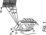
図1の参照番号10は、全体として、例えば携帯情報端末のようなハンドヘルドの機器を識別し、該ハンドヘルドの機器内に、図2に示されているような軽量でコンパクトな画像投影の装置20が取り付けられ、機器から様々な距離で二次元のカラー画像を投影するように動作する。例として、画像18が機器10に対して作業範囲の距離の中で位置を定められる。
Reference numeral 10 in FIG. 1 generally identifies a handheld device, such as a personal digital assistant, for example, within the handheld device, a lightweight and compact
図1に示されているように、画像18は、画像の水平方向に沿って伸びる光学的な水平方向の走査角度Aと、画像の垂直方向に沿って伸びる光学的な垂直方向の走査角度Bとを渡って伸びる。以下で記述されるように、画像は、装置20においてスキャナによって掃引される走査線のラスターパターン上の照明される画素と照明されない画素とから構成される。
As shown in FIG. 1, the
機器10の平行六面体の形状は、装置20が実装され得る筐体の1つの形状因子を表しているだけである。機器は、例えば、2002年3月4日出願の米国特許出願第10/090,653号に示されているように、ペン、セルラー電話、クラムシェル、または腕時計のように形作られ得、該出願は、本出願と同じ譲受人に譲渡され、かつ、本明細書において参考として援用される。
The shape of the parallelepiped of the device 10 represents only one form factor of the housing in which the
好適な実施形態において、装置20は体積が約30立方センチメートル未満である。このコンパクトな小型のサイズは、搭載ディスプレイ12と、キーパッド14と、ウインドウ16とを有する一部の筐体を含む、多種多様な形状の、大きいまたは小さい、ポータブルのまたは固定の筐体に、装置20が取り付けられることを可能にし、該ウインドウ16を通して画像は投影される。
In a preferred embodiment,
図2および図3を参照すると、装置20は半導体レーザ22を含み、該半導体レーザ22は起動されたときに、約635〜655ナノメートルの明るい赤色レーザビームを発する。レンズ24は、正の焦点距離を有する両面非球面(biaspheric)凸レンズであり、赤色ビームにおいて事実上全てのエネルギーを収集し、回折が限定されるビームを生成するように動作する。レンズ26は、負の焦点距離を有する凹レンズである。レンズ24、26は、例示されていないそれぞれのレンズホルダによって、機器10の内側の支持(簡潔さのために、図2には例示されていない)上に離れて保持されている。レンズ24、26は、作業距離に渡って赤色ビームのプロフィールを形作る。
2 and 3, the
別の半導体レーザ28が、支持の上に取り付けられ、起動されたときに、約475〜505ナノメートルで回折が限定された青色レーザビームを発する。別の両面非球面の凸レンズ30と凹レンズ32とが、レンズ24、26と同様の方法で青色ビームのプロフィールを形作るために利用される。
When another
およそ530ナノメートルの波長を有する緑色レーザビームは、半導体レーザによっては生成されないが、その代わりに出力ビームが1060nmである赤外線ダイオード励起YAG結晶レーザを有する緑色モジュール34によって生成される。非線形の周波数二倍化結晶が2つのレーザミラーの間の赤外線レーザキャビティに含まれる。キャビティの内側の赤外線レーザの出力は、キャビティの外側で結合される出力よりも非常に大きいので、周波数二倍器は、キャビティの内側で二倍化周波数の緑色の光を生成することにおいてより効率的である。レーザの出力ミラーは、1060ナノメートルの赤外線放射を反射し、二倍化された530nmの緑色レーザビームを伝える。固体レーザおよび周波数二倍器の正しい動作は、正確な温度制御を必要とするので、ペルチェ効果に依存する熱電冷却器のような半導体デバイスが、緑色レーザモジュールの温度を制御するために使用される。熱電冷却器は、印加された電流の極性に従ってデバイスを加熱または冷却のいずれかを行い得る。サーミスターは、温度を監視するために緑色レーザモジュールの一部分である。サーミスターからの読み出しがコントローラに供給され、該コントローラは、それに応じて、熱電性の冷却器に対する制御電流を調節する。
A green laser beam having a wavelength of approximately 530 nanometers is not generated by a semiconductor laser, but instead is generated by a
以下で述べられるように、レーザは約100MHzの周波数での動作においてパルス化される。赤色および青色の半導体レーザ22、28は、このような高い周波数で変調され得るが、現在利用可能な緑色固体レーザはパルス化され得ない。結果として、緑色モジュール34を出る緑色レーザビームは、音響光学変調器(AOM)36を用いてパルス化され、該音響光学変調器(AOM)36は、緑色ビームを回折するために結晶の内側で音響定常波を作成する。しかしながら、AOM36は、ゼロ次の回折されていないビーム38と、一次の変調された回折されたビーム40とを生成する。ビーム38、40は互いから分かれ、それらを分離し、所望されないゼロ次のビーム38を排除するために、ビーム38、40は、折り曲げミラー42を有する、曲がった長い経路に沿って伝送される。代替的に、AOMは、緑色レーザビームをパルス化するために、緑色レーザモジュールに対して外部または内部のいずれかで使用され得る。緑色レーザビームを変調する他の可能な方法は、電場吸収変調またはマッハツェンダー干渉計を含む。AOMは図2に概略的に示されている。
As described below, the laser is pulsed in operation at a frequency of about 100 MHz. Red and
ビーム38、40は、正のレンズ44と負のレンズ46とを通って伝送される。しかしながら、回折された緑色ビーム40だけが、折り曲げミラー48に衝突し、そこから反射することを可能にされる。回折されていないビーム38は、好適にはミラー48に取り付けられる吸収器50によって吸収される。
装置は、走査アセンブリ60に届く前に、緑色、青色、赤色のビームをできる限り同一線上にあるように配置させる一対のダイクロイックフィルタ52、54を含む。フィルタ52は、緑色ビーム40が通過することを可能にするが、青色レーザ28からの青色ビーム56は、干渉効果によって反射される。フィルタ54は、緑色ビーム40および青色ビーム56が通過することを可能にするが、赤色レーザ22からの赤色ビーム58は干渉効果によって反射される。
The apparatus includes a pair of
ほぼ同一直線のビーム40、56、58は、固定のバウンスミラー62に向けられ、そこで反射される。走査アセンブリ60は、第1の水平方向の走査角度Aに渡ってバウンスミラー62に反射されるレーザビームを掃引するために、第1の走査速度で、(図4〜図5に独立して示されている)慣性ドライブ66によって振動可能である第1の走査ミラー64と、第2の垂直方向の走査角度Bに渡って第1の走査ミラー64に反射されるレーザビームを掃引するために、第2の走査速度で、電磁デバイス70によって振動可能である第2の走査ミラー68とを含む。異なる構成において、走査ミラー64、68は単一の二軸のミラーによって置換され得る。
The substantially
慣性ドライブ66は、高速の低電力消費のコンポーネントである。慣性ドライブの詳細は、2003年3月13日出願の米国特許第10/387,878号に見つけられ得、該出願は本出願と同じ譲受人に譲渡され、本明細書において参考として援用される。慣性ドライブの使用は、走査アセンブリ60の電力消費を1ワット未満に減少させ、以下で記述されるように、カラー画像を投影する場合には、10ワット未満に減少させる。
Inertial drive 66 is a high speed, low power consumption component. Details of the inertial drive can be found in US patent application Ser. No. 10 / 387,878 filed Mar. 13, 2003, which is assigned to the same assignee as the present application and is incorporated herein by reference. . The use of an inertial drive reduces the power consumption of the
ドライブ66は、ヒンジによって走査ミラー64を支持するための可動なフレーム74を含み、該ヒンジは、一対の同一直線上にあるヒンジ部分76、78を含み、該ヒンジ部分76、78は、ヒンジの軸に沿って伸び、走査ミラー64の対向する領域とフレームの対向する領域との間で接続されている。フレーム74は、示されているように、走査ミラー64を囲む必要はない。
The
フレーム、ヒンジ部分、および走査ミラーは、約150μの厚さである一片の概ね平坦なシリコン基板で製造される。シリコンは、上部の平行なスロットセクションと、下部の平行なスロットセクションと、U字形状の中央のスロットセクションとを有するオメガ形状のスロットを形成するようにエッチングされる。走査ミラー64は、好適には、楕円形状を有し、スロットセクションにおいて自由に動く。好適な実施形態において、楕円形状の走査ミラーの軸に沿った大きさは、749μx1600μの寸法を取る。各ヒンジ部分は、幅27μかつ長さ1130μの寸法を取る。フレームは、幅3100μかつ長さ4600μの寸法を取る長方形形状を有する。
The frame, hinge portion, and scanning mirror are fabricated from a piece of generally flat silicon substrate that is approximately 150 microns thick. The silicon is etched to form an omega-shaped slot having an upper parallel slot section, a lower parallel slot section, and a U-shaped central slot section. The
慣性ドライブは、概ね平坦なプリント回路基板80上に取り付けられ、フレームを直接的に動かし、慣性によってヒンジの軸の周りで走査ミラー64を間接的に振動させるように動作する。慣性ドライブの一実施形態は、一対の圧電性トランスデューサ82、84を含み、該トランスデューサ82、84は、基板80に垂直に、かつヒンジ部分76のいずれかの側において、フレーム74の間隔を空けられた部分と接触するように延びる。各トランスデューサの一端と各フレーム部分との間の永久的な接触を確実にするために、接着剤が使用され得る。各トランスデューサの反対側の端部は、基板80の背面から突出し、ワイヤ86、88によって周期的な交流電源(図示されず)に電気的に接続される。
The inertial drive is mounted on a generally flat printed
使用において、周期的な信号が各トランスデューサに周期的なドライブ電圧を印加し、それぞれのトランスデューサを長手方向に交互に伸縮させる。トランスデューサ82が伸び、トランスデューサ84が縮むとき、およびその逆であるときには、それによって、間隔の空いたフレーム部分を同時に押したり引いたりし、フレームをヒンジの軸の周りでねじらせる。ドライブ電圧は、走査ミラーの共振周波数に対応する周波数を有する。走査ミラーがまた共振周波数でヒンジの軸の周りで振動するまで、走査ミラーは最初の停止位置から動く。好適な実施形態において、フレームと走査ミラーとは約150μの厚さであり、走査ミラーは高いQ値を有する。各トランスデューザによる約1μの動きが、20kHzを超える走査速度での走査ミラーの振動をもたらし得る。
In use, a periodic signal applies a periodic drive voltage to each transducer, causing each transducer to alternately expand and contract in the longitudinal direction. When the
別の対の圧電性のトランスデューサ90、92は基板80に垂直に、かつヒンジ部分78のいずれかの側でフレーム74の間隔の空いた部分と永久的に接触するように延びる。トランスデューサ90、92は、フレームの振動運動を監視し、フィードバック制御回路(図示されず)にワイヤ94、96に沿って電気的なフィードバック信号を生成し、導くフィードバックデバイスとして作用する。
Another pair of
代替的に、フィードバックのために圧電性トランスデューサ90、92を使用する代わりに、磁気フィードバックが使用され得、磁石が高速ミラーの後に取り付けられ、外部のコイルが、振動する磁石によって生成される変化する磁場をピックアップするために使用される。
Alternatively, instead of using
光は走査ミラーの外面で反射し得るが、金、銀、アルミニウム、または特別に設計された高反射性の誘電性のコーティングで作成される鏡面コーティングを用いて、ミラー64の表面をコーティングすることが望ましい。
The light can be reflected from the outer surface of the scanning mirror, but the surface of the
(図8において分解図で示され、図9において組み立て図で示された)電磁ドライブ70は、屈曲部200と第2の走査ミラー68の背面とに接合するように取り付けられる永久磁石71と、周期的なドライブ信号の受信に応答して周期的な磁場を生成するように動作する電磁コイル72とを含む。コイル72は磁石71に隣接しており、その結果、周期的な磁場が永久磁場と磁気的に相互作用し、以下で詳細に記述されるように、磁石、同時に第2の走査ミラー68を振動させる。
The electromagnetic drive 70 (shown in an exploded view in FIG. 8 and in an assembled view in FIG. 9) includes a
慣性ドライブ66は、好適には5kHzを上回る、さらに好適には約18kHz以上の走査速度で、走査ミラー64を高速で振動させる。この高い走査速度は、不可聴周波数であり、それによりノイズおよび震動を最小化する。電磁ドライブ70は、過度なちらつきがなく画像が人間の網膜に残ることを可能にする充分な速さよりも小さい走査速度で、走査ミラー68を振動させる。
Inertial drive 66
より速いミラー64は水平方向の走査線を掃引し、より遅いミラー68は水平方向の走査線を垂直に掃引し、それによりほぼ平行な走査線のグリッドまたはシーケンスであるラスターパターンを作成し、該ほぼ平行な走査線のグリッドまたはシーケンスから画像が構成される。各走査線は多数の画素を有する。画像の解像度は、好適には、1024x768画素のXGA品質である。限定された作業範囲を超えて、720p、1270x720画素を示す高精細度のテレビ規格を表示し得る。一部の用途においては、VGA品質の二分の一の320x480画素、またはVGA品質の四分の一の320x240画素で充分である。最低でも、160x160画素の解像度が所望される。
The
ミラー64、68の役割は逆にされ得、その結果、ミラー68がより速くなり、ミラー64がより遅くなる。ミラー64は垂直方向の走査線を掃引するようにも設計され得、その場合、ミラー68は水平方向の走査線を掃引する。さらに、慣性ドライブはミラー68を駆動するために使用され得る。実際、いずれかのミラーが、電子機械的、電気的、機械的、静電気的、磁気的、または電磁的なドライブによって駆動され得る。
The roles of the
遅いミラーは、画像が表示される時間の間に、図11に関して以下で記述されるように、一定速度の掃引モードで動作される。ミラーの戻りの間に、有意に高い固有周波数または共振周波数において、ミラーは最初の位置に掃引される。ミラーの帰路の間に、レーザは、デバイスの電力消費を減少させるために、パワーダウンされ得る。 The slow mirror is operated in a constant speed sweep mode during the time that the image is displayed, as described below with respect to FIG. During mirror return, the mirror is swept to the initial position at a significantly higher natural or resonant frequency. During the mirror return, the laser can be powered down to reduce the power consumption of the device.
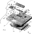
図6は、図2の斜視図と同じ斜視図における装置20の実際の実装である。上記のコンポーネントが、上部カバー100と支持プレート102とを含む支持に取り付けられる。ホルダ104、106、108、110、112はそれぞれ、折り曲げミラー42、48と、フィルタ52、54と、バウンスミラー62とを互いに一直線に保持している。各ホルダは、支持に固定して取り付けられる位置決めポストを受け取る複数の位置決めスロットを有する。従って、ミラーとフィルタとは正確に位置決めされる。示されているように、3つのポストがあり、それにより2つの角度調節と1つの横方向の調節とを可能にする。各ホルダは最終的な配置で接着され得る。
FIG. 6 is an actual implementation of the
画像は1つ以上の走査線における画素の選択的な照明によって構成される。図7を参照してさらに詳細に以下で記述されるように、コントローラ114は、3つのレーザビームによって、ラスターパターンにおいて選択された画素を照明して、視認可能にさせる。例えば、赤色出力コントローラ116、青色出力コントローラ118、および緑色出力コントローラ120は、各選択された画素にそれぞれの光ビームを発するためにそれぞれ、赤色レーザ22、青色レーザ28、および緑色レーザ34に電流を伝え、赤色レーザ22、青色レーザ28、および緑色レーザ34を起動し、他の選択されていない画素を照明しないために、赤色レーザ、青色レーザ、および緑色レーザに電流を伝えず、赤色レーザ、青色レーザ、および緑色レーザを切断する。照明された画素と照明されない画素との結果としてのパターンは画像を含み、該画像は、人間または機械が読み取り可能な情報または図形の任意の表示であり得る。
The image is composed of selective illumination of pixels in one or more scan lines. As described in more detail below with reference to FIG. 7, the
図1を参照すると、ラスターパターンが拡大図で示されている。エンドポイントから開始すると、レーザビームが、慣性ドライブによって、反対側のエンドポイントに水平方向の走査速度で、水平方向に沿って掃引され、走査線を形成する。その結果、レーザビームは、電磁ドライブ70によって、別のエンドポイントに垂直方向の走査速度で、垂直方向に沿って掃引され、第2の走査線を形成する。次の走査線の編成は同じ方法で進行する。
Referring to FIG. 1, the raster pattern is shown in an enlarged view. Starting from the end point, the laser beam is swept along the horizontal direction by an inertial drive to the opposite end point at a horizontal scan rate to form a scan line. As a result, the laser beam is swept along the vertical direction by the
画像は、マイクロプロセッサ114または制御回路の制御の下で、出力コントローラ116、118、120の動作によって、選択された回数、断続的にレーザを起動またはパルス化することによって、ラスターパターンで作成される。レーザは可視光を生成し、所望の画像内の画素が見られることを所望されるときに点灯される。各画素の色は、一色以上のビームによって決定される。可視光のスペクトルにおける任意の色が、赤色レーザ、青色レーザ、および緑色レーザのうちの1つ以上の選択的な重ね合わせによって形成され得る。ラスターパターンは、各走査線上の複数の画素と複数の線とで作られるグリッドである。画像は、選択された画素のビットマップである。全ての文字または数字、任意の図形設計またはロゴ、機械で読み取り可能なバーコード記号でさえも、ビットマップ画像として形成され得る。
The image is created in a raster pattern by intermittently activating or pulsing the laser a selected number of times by operation of the
図7に示されているように、垂直方向および水平方向の同期データと、画素およびクロックのデータとを有する入力ビデオ信号は、マイクロプロセッサ114の制御の下で、赤色バッファ122、青色バッファ124および緑色バッファ126に送られる。1つの最大のVGAフレームの格納は数キロバイトを必要とし、2つの最大のフレームが、別のフレームが処理され投影される間に、1つのフレームが書き込まれることを可能にするように、バッファ内に充分なメモリを有することが望ましい。バッファリングされたデータは、速度プロファイラ130の制御の下でフォーマッタ128に送られ、そして赤色ルックアップテーブル(LUT)132、青色ルックアップテーブル(LUT)134および緑色ルックアップテーブル(LUT)136に送られ、走査によってもたらされる固有の内部的な歪み、および投影された画像の表示角度によってもたらされる幾何形状的な歪みを補正する。結果としての赤色デジタル信号、青色デジタル信号および緑色デジタル信号が、デジタルアナログ変換器(DAC)138、140、142によって、赤色アナログ信号、青色アナログ信号および緑色アナログ信号に変換される。赤色アナログ信号および青色アナログ信号は、赤色レーザドライブ144および青色レーザドライブ146に供給され、該赤色レーザドライブ(LD)144および該青色レーザドライブ(LD)146はまた、赤色出力コントローラ116および青色出力コントローラ118に接続される。緑色アナログ信号は、AOM無線周波数(RF)ドライブ150に供給され、次に、緑色レーザ34に供給され、該緑色レーザ34はまた、緑色LD148および緑色電力コントローラ120に接続される。
As shown in FIG. 7, an input video signal having vertical and horizontal synchronization data and pixel and clock data is controlled under the control of a
赤色アナログデジタル(A/D)変換器158、青色アナログデジタル(A/D)変換器160および緑色アナログデジタル(A/D)変換器162に接続され、次にマイクロプロセッサ114に接続される赤色フォトダイオード増幅器152、青色フォトダイオード増幅器154および緑色フォトダイオード増幅器156を含むフィードバック制御がまた図7に示されている。A/D変換器166に接続され、次にマイクロプロセッサに接続されるサーミスター増幅器164によって、熱が監視される。
A red photo connected to a red analog-to-digital (A / D)
走査ミラー64、68はドライブ168、170によって駆動され、該ドライブ168、170は、DAC172、174からアナログドライブ信号を供給され、次に、該DAC172、174はマイクロプロセッサに接続される。フィードバック増幅器176、178は、走査ミラー64、68の位置を検出し、フィードバックA/D180、182に接続され、次に、マイクロプロセッサに接続される。
The scanning mirrors 64, 68 are driven by
電力管理回路184は、好適には、緑色レーザを常時オンにしたままで保ち、かつ、赤色レーザおよび青色レーザをレージングの閾値のすぐ下に保つことによって、高速のオンタイムを可能にしつつ、電力を最小化するように動作する。
The
走査ミラー64、68のいずれかが位置を外れていると検出された場合に、レーザ安全切断回路186は、レーザを止めるように動作する。
If it is detected that either of the scanning mirrors 64, 68 is out of position, the laser
ここで、図8〜図9の電磁ドライブ70を参照すると、上で記述された屈曲部200は、平坦な支持部分202と、一対の平坦な同一直線上のねじれ部分204、206と、一対の平坦な端部208、210とを含む。屈曲部は、弾性材料の単一の細長片であり、好適には、約0.027mmの厚さを有する鍛えられたステンレス鋼である。ねじれ部分の幅は約0.122mmであり、このような寸法を有する屈曲部を機械加工することは可能であるが、この目的のためには、屈曲部を化学的にエッチングすることが好ましい。以下で記述されるように、走査ミラー68の共振周波数を調節するように制御されるのは、ねじれ部分の横方向の寸法である。ねじれ部分は、以下で記述されるように、ねじれバーとして機能する薄く長いワイヤ状のストランドである。
Referring now to the
ドライブ70は、上部プレート212と下部プレート214とを有する成形されたプラスチックの支持を含み、該上部プレート212と該下部プレート214との間に、コイル72は挟まれる。上部プレートは、上部開口と、狭い概ね長方形の窪み222に取り付けられた一対の直立した円筒形の位置決めピン218、220と、別の狭い窪み226に取り付けられた直立した突起224とを有する細長い窪んだ区画216を有する。
The
屈曲部200は、上部プレート212に取り付けられ、区画216の上部開口に長手方向にかかる。磁石71は、支持部分202の底側に取り付けられ、少なくとも部分的には、区画216の中にあり、それにより磁石71をこれまでよりもコイルの近くで位置決め氏、ドライブに対して必要とされる全体的な垂直方向の高さを低くする。
The
端の領域208は、E字形状であり、ピン220、218をきちんと受ける一対のカットアウト228、230を有する。嵌め込み穴232、234は、液体の接着剤の導入が、狭い窪み222において端の領域208をしっかりと固定することを可能にする。
The
端の領域210は、長方形として形作られ、長手方向の切り込み236、238と横断方向の切り込み240とによって内部に形成され、それにより長方形のフラップ242を形作りかつ作成する。フラップ242は端の領域210と同一平面にある。しかしながら、例示の簡潔さのために、図8のフラップ242は、以下で記述されるように、ピンと張った状態で端の領域210の平面の上にある自由端244をより良く表示するために、湾曲された、圧縮された、または曲げられた状態で示されている。フラップ242は、自由端244に平行である蝶番式の端246において端の領域210に対して蝶番式に取り付けられる。
The
端の領域210が上部プレート212に取り付けられたときに、上記の突起224の上面250は、自由端244に隣接するフラップの下側に係合し、フラップを押し、例示された湾曲形状をとる。フラップが曲げられると、フラップは、端の領域210における長方形のカットアウト248を空にする。突起224はまた、曲がったフラップ242の湾曲に対して概ね補完的な外形である湾曲面252を有する。実際に、屈曲部がピンセットのような道具を用いて手動で設置された場合であっても、組み立ての間に、曲がったフラップ242が降伏点を越えて曲がらないことを確実にするように、湾曲面252は設計されている。言い換えると、このような永久的な歪みは、以下で記述されるように、フラップから屈曲部に対して必要な張力を提供することを奪い得るので、フラップに対して永久的な曲げを与えることは所望されない。さらに、落下イベント、つまり装置が偶発的に地面または他の固い面にぶつかったときに、装置が突然の衝撃と減速力とを経験する場合であっても、湾曲面252と湾曲したフラップ242との間の限られた隙間は、永久的な曲げがフラップには与えられないことを確実にする。
When the
図9の組み立て図に示されるように、端の領域210が上部プレート212に平らに置かれると、自由端244は、突起250の直立した垂直面256と湾曲面252との間に形成されるコーナー254において、スナップ型の動きで捕らえられる。突起224は弾性的なフラップ242と協働して、屈曲部の長手方向に張力を加える。つまり、端の領域210は端の領域208から離れるように押される。この張力は、従来技術のように追加の別個のコンポーネントによって達成されるのではなく、その代わりに屈曲部に組み込まれるフラップによって達成される。屈曲部のねじれ部分をピンと張る反作用力を作り出すものは、フラップの圧縮または縮みである。
As shown in the assembly diagram of FIG. 9, when
張力の加えられた屈曲部は、上に取り付けられた走査ミラー68に対する復元スプリングとして働く。周期的なドライブ信号を用いたコイル72の起動の間、周期的な電磁場が伝搬され、磁石71の永久的な磁場と相互作用することにより、ねじれ部分204、206が伸びる軸に沿って一円周方向に磁石を動かす。磁石は、支持部分202と走査ミラー68とを動かし、固定された端部208、210に対する軸の周りで一円周方向に、端部限界(end−limiting)走査位置までねじれ部分204、206をひねる。そこで、ひねられたねじれ部分に格納されたエネルギーが解放され、それにより支持部分202と走査ミラー68とを動かし、固定された端部部分208、210に対する軸の周りで反対の円周方向に、ねじれ部分のひねりを戻す。このエネルギーの解放は、相互作用する磁場によって補助され得たり、補助され得なかったりする。いかなる場合においても、支持部分202および走査ミラーの運動は共振周波数で継続し、ねじれ部分204、206が、今回は、反対の円周方向に沿って別の端部限界走査位置までひねられる。このサイクルは繰り返され、それにより走査ミラー68を振動し、端部限界走査位置の間で走査ミラー68に入射する任意の光ビームを掃引する。屈曲部が引っ張られることを確実にすることによって、ミラーの走査運動は、繰り返すことが可能となり、信頼性があり、金属の屈曲部の膨張および収縮をもたらす周囲の温度変化に対して反応を示さない。
The tensioned bend acts as a restoring spring for the
一対の震動ダンパー258、260が、端の領域210および上部プレート212に取り付けられる。ダンパーは、特定の周波数範囲内のあらゆる震動を弱めるように設計された粘弾性のダンパーとして作用する。ダンパーはまた、落下イベントの間に、屈曲部が突起224から取り除かれることに抵抗するために、端部領域210に対する追加の機械的固定具として作用する。
A pair of
上に記したように、好適な実施形態において、本発明のコンパクトなドライブは、ラスターパターンを作成することにおいて、垂直方向つまりY軸方向のドライブとして使用される。これは、走査ミラーに入射する光ビームが、その長さがラスターパターンの水平方向つまりX軸方向に沿って伸びる走査線であるということを意味する。走査線の全長を収容するために、図8〜図9に示されているように、走査ミラー68は長さが長く、高さが低い。しかしながら、長い走査ミラーはドライブの全長を増加させるので、従って、全長を減らし、それによりコンパクトな構成を達成するために、走査ミラーは、少なくとも部分的には、ねじれ部分204、206に重なるように設計される。このために、図10に示されているように、走査ミラー68の背部は、長手方向の窪み262を有し、その結果、ねじれ部分204、206は、重なる領域において走査ミラーに接触しない。
As noted above, in a preferred embodiment, the compact drive of the present invention is used as a vertical or Y-axis drive in creating a raster pattern. This means that the light beam incident on the scanning mirror is a scanning line whose length extends along the horizontal direction of the raster pattern, that is, the X-axis direction. In order to accommodate the entire length of the scanning line, the
図10に示されているように、走査ミラー68はT字形状の断面を有し、プラスチックの押し出し成形部品またはガラスの伸ばし成形部品であることが好ましく、その上に反射ミラーコーティングがコーティングされる。長い押し出し成形が製造され、磨かれ、コーティングされ、ドライブ内での使用のために切断され得る。
As shown in FIG. 10, the
図11にグラフで描かれているように、走査ミラー68は、ドライブサイクルの一部分の間に、電磁ドライブ70によって実質的に一定の速度でドライブモードで駆動され、その時間の間に、画像の1つのフレームが表示される。例えば、これは、ラスターパターンにおける最も高い位置から最も低い位置まで、またはその逆の走査線の運動を表す。図11はまた、ドライブサイクルの残りの部分の間に走査ミラーが戻るミラーのリターンモードを描く。これは、ラスターパターンにおける最も低い位置から最も高い位置まで、またはその逆の走査線の運動を表す。戻ることは、電力を保つために、走査ミラー68の共振周波数で行われ、示されているように、ドライブモードの間のドライブ70のドライブ周波数よりも速い。
As depicted graphically in FIG. 11, the
数値的な例によって先に言及されたように、一般的なドライブ周波数、すなわちフレームレートは60Hzまたは85Hzであるが、56Hz、72Hzおよび75Hzのような他の周波数がまた、多くの場合に使用される。電磁コイル70を作動するためのACライン周波数は、一般的に、50Hzまたは60Hzである。ドライブ周波数またはライン周波数の調波が、走査ミラー68の共振周波数にぴったりと一致する場合には、電気的干渉が存在し、図12に描かれているように、正弦曲線状の過渡が、速度対時間のグラフの一定速度の部分に重ねられる。歪みのない画像は、ドライブモードの間、速度が実質的に一定であることが必要である。しかしながら、過渡は速度に関する変化をもたらし、それにより制御されず予測できないように画像を歪ませる。
As mentioned earlier by numerical examples, typical drive frequencies, ie frame rates, are 60 Hz or 85 Hz, but other frequencies such as 56 Hz, 72 Hz and 75 Hz are also often used. The The AC line frequency for operating the
本発明に従って、共振周波数は、可能である限りドライブ周波数またはライン周波数の調波から特定のトレードオフを受けるように調節される。共振周波数は、走査ミラー68の素早い戻りを確実にするためにできる限り高くあるべきだが、ドライブ70による電力消費を最小化するようにできる限り低くあるべきである。好適な実施形態において、共振周波数は、270〜280Hzの範囲にあるように選択される。
In accordance with the present invention, the resonant frequency is adjusted to receive a specific trade-off from the drive frequency or line frequency harmonics whenever possible. The resonant frequency should be as high as possible to ensure quick return of the
走査ミラー68の共振周波数は、ミラー68の質量、および/または磁石71の質量、および/または屈曲部200の材料のような要素を変更することによって調節可能である。しかしながら、このような要素を一定に維持し、その代わりにねじれ部分204、206の厚さおよび/または幅を変化させることが好ましい。上に記されたように、ねじれ部分のごくわずかな厚さは約0.027mmであり、幅は約0.122mmである。これらの横方向の寸法を達成するために化学的エッチングが、ドライブ周波数およびライン周波数の整数の倍数ではない所望の共振周波数を取得するために好まれる。
The resonant frequency of the
図13は、一円周方向に実質的に一定の速度で走査ミラー68を駆動し、反対の円周方行に共振周波数で素早く元に戻る運動を可能にするように動作するドライブ回路の実施形態を描く。フィードバックユニット300は、フィードバック信号から速度および位置の情報を抽出し、誤差増幅器304への入力のための速度信号と、コンパレータ306への入力のための位置信号とを生成する。フィードバックユニット300は、一般的に、磁石71の近位に取り付けられ、かつ、フィードバック信号を生成するように動作するフィードバックコイルを含み、該フィードバック信号は、ドライブコイル72によって生成されたドライブ信号を追跡する。
FIG. 13 illustrates an embodiment of a drive circuit that operates to drive the
ミラーコントローラ302は望ましい速度を設定し、ミラーの速度信号との比較のために、誤差増幅器304に基準速度信号を出力する。走査増幅器304の出力はミラードライバ308に供給され、該ミラードライバ308は、コントローラ302によって設定された基準速度に一致するように走査ミラーの速度を継続的に調節するために、ドライブコイル72に対して出力ドライブ電流を生成する。
The
コントローラ302はまた、端部限界位置を設定し、ミラーの位置信号との比較のために、コンパレータ306に対して端の位置の信号を出力する。コンパレータ306の出力はまた、ミラードライバ308に供給される。ミラーの位置の信号が、端部位置の信号に一致するときには、ミラードライバ308は、高いインピーダンスの状態に切り換えられ、それによりドライブコイル72に対する出力ドライブ電流の流れを防ぐ。従って、走査ミラー68は、ひねられたねじれ部分に格納されたエネルギーによって、共振周波数で自由であるように設定される。走査ミラーが、反対側の端部限界位置に到達したときには、コンパレータ306はミラードライバ308を戻るように切り替え、新たなドライブサイクルが開始する。
The
図14の実施形態は図13の実施形態と同様であるが、ミラードライバ308が、ミラーコントローラ302の完全な制御下にある点で異なる。この実施形態において、ドライバ308を継続的に調節する代わりに、コントローラ302が、連続するサイクルに対してわずかな増分変更をさせる間に、所定のサイクルを繰り返す。任意的に、コントローラ302は、ホストコントローラからの垂直方向の同期パルスに同期される。
The embodiment of FIG. 14 is similar to the embodiment of FIG. 13 except that the
新規的であると主張され、かつ、特許証によって保護されることが所望されることが、添付の特許請求の範囲において述べられる。 What is claimed as novel and desired to be protected by Letters Patent is set forth in the appended claims.
Claims (5)
光のビームを生成する光源と、
一対の振動可能な走査ミラーと、
投影面において走査線のラスターパターンを形成するために、互いに直交する軸の周りで該走査ミラーを振動させるためのドライブアセンブリであって、各走査線は多数の画素を有し、該ドライブアセンブリは、供給ライン周波数によって起動され、かつ実質的に一定のドライブ速度で該軸のうちの1つの周りを一円周方向に、該走査ミラーのうちの1つを動かすためのドライブ周波数で動作可能なドライブを含み、該1つの走査ミラーは、該ドライブ速度よりも大きい戻り速度で該1つの軸の周りを反対の円周方向に共振周波数で戻ることが可能である、ドライブアセンブリと、
該投影面に該画像を形成するために、該レーザビームによって、該走査線において選択された画素を照明して、視認可能なようにさせるためのコントローラと、
該共振周波数と該ドライブ周波数と、該供給ライン周波数との間の電気的干渉を減少させ、画像の歪みに影響されないようにするために、該ドライブ周波数および該供給ライン周波数に関して調和しないように該共振周波数を調節する手段と
を備えている、装置。An apparatus for reducing image distortion in a projected image, comprising:
A light source that generates a beam of light;
And oscillatable scan mirror for a pair,
To form a raster pattern of scan lines in the projected Kagemen, a drive assembly for vibrating said scanning mirror about an axis orthogonal to each other, each scan line has a number of pixels, said drive assembly Is activated by the supply line frequency and is operable at a drive frequency for moving one of the scanning mirrors in a circumferential direction around one of the axes at a substantially constant drive speed A drive assembly, wherein the one scanning mirror is capable of returning at a resonant frequency in an opposite circumferential direction about the one axis at a return speed greater than the drive speed;
To form the image on the projection plane, a controller for the said laser beam, to illuminate the selected pixels to have you in the scanning line, thereby to allow viewing,
And said resonant frequency and said drive frequency, to reduce the electrical interference between the supply line frequency, in order to not be affected in the distortion of the image, the so inconsistent with respect to the drive frequency and the feed line frequency Means for adjusting the resonant frequency.
Applications Claiming Priority (2)
| Application Number | Priority Date | Filing Date | Title |
|---|---|---|---|
| US11/165,737 US7307650B2 (en) | 2005-06-24 | 2005-06-24 | Arrangement for, and a method of, reducing image distortion due to electrical interference |
| PCT/US2006/019502 WO2007001681A2 (en) | 2005-06-24 | 2006-05-19 | An arrangement for, and a method of, reducing image distortion due to electrical interference |
Publications (3)
| Publication Number | Publication Date |
|---|---|
| JP2008547055A JP2008547055A (en) | 2008-12-25 |
| JP2008547055A5 JP2008547055A5 (en) | 2009-09-24 |
| JP4674313B2 true JP4674313B2 (en) | 2011-04-20 |
Family
ID=37566818
Family Applications (1)
| Application Number | Title | Priority Date | Filing Date |
|---|---|---|---|
| JP2008518171A Expired - Fee Related JP4674313B2 (en) | 2005-06-24 | 2006-05-19 | Apparatus and method for reducing image distortion due to electrical interference |
Country Status (5)
| Country | Link |
|---|---|
| US (1) | US7307650B2 (en) |
| JP (1) | JP4674313B2 (en) |
| CN (1) | CN101583905B (en) |
| DE (1) | DE112006001670T5 (en) |
| WO (1) | WO2007001681A2 (en) |
Families Citing this family (9)
| Publication number | Priority date | Publication date | Assignee | Title |
|---|---|---|---|---|
| US7815119B2 (en) * | 2006-06-06 | 2010-10-19 | Symbol Technologies, Inc. | Monitoring scan mirror motion in laser scanning arrangements |
| US7997742B2 (en) * | 2008-03-25 | 2011-08-16 | Microvision, Inc. | Capacitive comb feedback for high speed scan mirror |
| US20090251670A1 (en) * | 2008-04-03 | 2009-10-08 | Motorola, Inc. | Optical feedback for high speed scan mirror |
| US8107147B2 (en) * | 2009-03-27 | 2012-01-31 | Microvision, Inc. | Two-mirror scanning system |
| JP2013171226A (en) | 2012-02-22 | 2013-09-02 | Funai Electric Co Ltd | Image display device and mirror driving method of the same |
| CN103809351B (en) * | 2012-11-09 | 2016-01-20 | 光宝科技股份有限公司 | Tool detects optical projection system and the detection method thereof of projected picture distortion |
| US8988475B2 (en) * | 2013-03-14 | 2015-03-24 | Mayadah ALHASHEM | Inkless printer |
| US10349025B2 (en) * | 2017-07-27 | 2019-07-09 | Seiko Epson Corporation | Projector and method of controlling projector |
| CN110703553B (en) * | 2018-07-09 | 2022-05-10 | 青岛海信激光显示股份有限公司 | Laser projection device |
Citations (5)
| Publication number | Priority date | Publication date | Assignee | Title |
|---|---|---|---|---|
| US6245590B1 (en) * | 1999-08-05 | 2001-06-12 | Microvision Inc. | Frequency tunable resonant scanner and method of making |
| JP2004020873A (en) * | 2002-06-14 | 2004-01-22 | Nippon Signal Co Ltd:The | Laser irradiation apparatus |
| JP2004527798A (en) * | 2001-05-15 | 2004-09-09 | マイクロビジョン インコーポレイテッド | Apparatus and method for producing an image on a screen using an erasing (off) and imaging (on) light source |
| JP2004264670A (en) * | 2003-03-03 | 2004-09-24 | Canon Inc | Optical deflector |
| JP2005526288A (en) * | 2002-05-15 | 2005-09-02 | シンボル テクノロジーズ インコーポレイテッド | High resolution image projection |
Family Cites Families (9)
| Publication number | Priority date | Publication date | Assignee | Title |
|---|---|---|---|---|
| US4387297B1 (en) * | 1980-02-29 | 1995-09-12 | Symbol Technologies Inc | Portable laser scanning system and scanning methods |
| US4732440A (en) * | 1985-10-22 | 1988-03-22 | Gadhok Jagmohan S | Self resonant scanning device |
| US5483025A (en) * | 1989-11-27 | 1996-01-09 | Censtor Corporation | Unitary micro-flexure structure |
| US6183092B1 (en) * | 1998-05-01 | 2001-02-06 | Diane Troyer | Laser projection apparatus with liquid-crystal light valves and scanning reading beam |
| JPH11327516A (en) * | 1998-05-13 | 1999-11-26 | Digital Electronics Corp | Display device |
| CN1484818A (en) * | 2000-10-27 | 2004-03-24 | Light beam display with interlaced light beam scanning | |
| US7441902B2 (en) * | 2004-10-27 | 2008-10-28 | Symbol Technologies, Inc. | Large size image projection |
| US7006274B1 (en) * | 2004-12-07 | 2006-02-28 | Symbol Technologies, Inc. | Compact acousto-optical modulator |
| US7227294B2 (en) * | 2005-04-29 | 2007-06-05 | Symbol Technologies, Inc. | Piezoelectric motor drive circuit and method |
-
2005
- 2005-06-24 US US11/165,737 patent/US7307650B2/en active Active
-
2006
- 2006-05-19 JP JP2008518171A patent/JP4674313B2/en not_active Expired - Fee Related
- 2006-05-19 CN CN2006800268199A patent/CN101583905B/en not_active Expired - Fee Related
- 2006-05-19 DE DE112006001670T patent/DE112006001670T5/en not_active Withdrawn
- 2006-05-19 WO PCT/US2006/019502 patent/WO2007001681A2/en active Application Filing
Patent Citations (5)
| Publication number | Priority date | Publication date | Assignee | Title |
|---|---|---|---|---|
| US6245590B1 (en) * | 1999-08-05 | 2001-06-12 | Microvision Inc. | Frequency tunable resonant scanner and method of making |
| JP2004527798A (en) * | 2001-05-15 | 2004-09-09 | マイクロビジョン インコーポレイテッド | Apparatus and method for producing an image on a screen using an erasing (off) and imaging (on) light source |
| JP2005526288A (en) * | 2002-05-15 | 2005-09-02 | シンボル テクノロジーズ インコーポレイテッド | High resolution image projection |
| JP2004020873A (en) * | 2002-06-14 | 2004-01-22 | Nippon Signal Co Ltd:The | Laser irradiation apparatus |
| JP2004264670A (en) * | 2003-03-03 | 2004-09-24 | Canon Inc | Optical deflector |
Also Published As
| Publication number | Publication date |
|---|---|
| WO2007001681A2 (en) | 2007-01-04 |
| CN101583905B (en) | 2010-11-17 |
| WO2007001681A3 (en) | 2009-04-30 |
| CN101583905A (en) | 2009-11-18 |
| JP2008547055A (en) | 2008-12-25 |
| US20060290774A1 (en) | 2006-12-28 |
| US7307650B2 (en) | 2007-12-11 |
| DE112006001670T5 (en) | 2008-05-15 |
Similar Documents
| Publication | Publication Date | Title |
|---|---|---|
| JP4674313B2 (en) | Apparatus and method for reducing image distortion due to electrical interference | |
| US7416126B2 (en) | Taut, torsional flexure and a compact drive for, and method of, scanning light using the flexure | |
| JP5213251B2 (en) | Correction for image distortion in image projectors | |
| JP2008529069A (en) | Apparatus and method for projecting a color image | |
| US7859600B2 (en) | Arrangement for and method of projecting a level image | |
| JP4931254B2 (en) | Piezoelectric motor drive circuit and method | |
| US7665853B2 (en) | Arrangement for, and method of, enhancing image projection by holding scan mirror steady during part of mirror drive cycle | |
| JP2008537162A (en) | Array and method for focusing a laser beam | |
| KR101020072B1 (en) | Arrangement for and method of projecting an image with linear scan lines | |
| US20070070309A1 (en) | Color image projection arrangement and method employing electro-absorption modulated green laser system | |
| US7329008B2 (en) | Shock-resistant arrangement for, and method of, protecting a heat source from damage | |
| JP2008539464A (en) | Scanline alignment in raster patterns | |
| US7460287B2 (en) | Arrangement for and method of increasing pixel symmetry, especially for image projection arrangements | |
| JP2009540360A (en) | Apparatus and method for projecting an image viewed over an extended viewing distance | |
| US20070273843A1 (en) | Arrangement for, and method of, increasing brightness of a projected image with drive-assisted flyback | |
| US20110090467A1 (en) | Image Projection Arrangement with Divergent Light Beams | |
| US20080204541A1 (en) | Aperture stop in an image projection arrangement for preserving color fidelity over an image | |
| JP2008535021A (en) | Compact acousto-optic modulator |
Legal Events
| Date | Code | Title | Description |
|---|---|---|---|
| A521 | Written amendment |
Free format text: JAPANESE INTERMEDIATE CODE: A523 Effective date: 20090430 |
|
| A621 | Written request for application examination |
Free format text: JAPANESE INTERMEDIATE CODE: A621 Effective date: 20090430 |
|
| A521 | Written amendment |
Free format text: JAPANESE INTERMEDIATE CODE: A523 Effective date: 20100419 |
|
| A977 | Report on retrieval |
Free format text: JAPANESE INTERMEDIATE CODE: A971007 Effective date: 20101101 |
|
| TRDD | Decision of grant or rejection written | ||
| A01 | Written decision to grant a patent or to grant a registration (utility model) |
Free format text: JAPANESE INTERMEDIATE CODE: A01 Effective date: 20101124 |
|
| A01 | Written decision to grant a patent or to grant a registration (utility model) |
Free format text: JAPANESE INTERMEDIATE CODE: A01 |
|
| A711 | Notification of change in applicant |
Free format text: JAPANESE INTERMEDIATE CODE: A711 Effective date: 20101221 |
|
| A61 | First payment of annual fees (during grant procedure) |
Free format text: JAPANESE INTERMEDIATE CODE: A61 Effective date: 20101222 |
|
| FPAY | Renewal fee payment (event date is renewal date of database) |
Free format text: PAYMENT UNTIL: 20140204 Year of fee payment: 3 |
|
| R150 | Certificate of patent or registration of utility model |
Free format text: JAPANESE INTERMEDIATE CODE: R150 |
|
| LAPS | Cancellation because of no payment of annual fees |