JP4670364B2 - Optical communication device - Google Patents
Optical communication device Download PDFInfo
- Publication number
- JP4670364B2 JP4670364B2 JP2005014167A JP2005014167A JP4670364B2 JP 4670364 B2 JP4670364 B2 JP 4670364B2 JP 2005014167 A JP2005014167 A JP 2005014167A JP 2005014167 A JP2005014167 A JP 2005014167A JP 4670364 B2 JP4670364 B2 JP 4670364B2
- Authority
- JP
- Japan
- Prior art keywords
- emission intensity
- light
- information
- optical
- light emission
- Prior art date
- Legal status (The legal status is an assumption and is not a legal conclusion. Google has not performed a legal analysis and makes no representation as to the accuracy of the status listed.)
- Expired - Fee Related
Links
Images


Landscapes
- Optical Communication System (AREA)
Description
本発明は、光通信装置に係り、特に、各々異なる光ファイバを介して複数の第2装置と各々接続された分配型光信号伝送体と光ファイバを介して接続され、複数の第2装置の各々へ光通信によって情報を送信可能な光通信装置に関する。 The present invention relates to an optical communication device, and more particularly, to a distributed optical signal transmission body connected to a plurality of second devices through different optical fibers, respectively, and to the plurality of second devices. The present invention relates to an optical communication apparatus capable of transmitting information to each by optical communication.
従来、入射された信号光を拡散させて伝播させる層状の導波路に、信号光の入出射を担う信号光入出射部が複数形成されて構成され、入射された光信号を複数の分配先へ分配可能な分配型光信号伝送体(以下、光シートバスともいう。)と、この分配型光信号伝送体を含んで構成された光通信システムとが提案されている(特許文献1〜6を参照)。 Conventionally, a layered waveguide that diffuses and propagates incident signal light is formed by forming a plurality of signal light input / output portions that are responsible for input / output of signal light, and the incident optical signal is distributed to a plurality of distribution destinations. Distributable distribution type optical signal transmission bodies (hereinafter also referred to as optical sheet buses) and an optical communication system including the distribution type optical signal transmission bodies have been proposed (see Patent Documents 1 to 6). reference).
レーザ光等の指向性の強い光信号を分配する場合、以前は光信号を一旦電気信号に変換して分配した後、分配した電気信号を、各分配先に対応して設けられた複数の発光素子によって各分配先へ光信号として送信する等の複雑な構成を必要としていたが、上記の分配型光信号伝送体を用いることで、指向性の強い光信号も直接分配することが可能となり、光通信システムの構成を簡単にすることができる。 When distributing highly directional optical signals such as laser light, the optical signal was previously converted into electrical signals and distributed, and then the distributed electrical signals are sent to a plurality of light sources provided corresponding to each distribution destination. Although a complicated configuration such as transmitting an optical signal to each distribution destination by an element was required, it becomes possible to directly distribute an optical signal with strong directivity by using the above-described distribution type optical signal transmitter, The configuration of the optical communication system can be simplified.
また、分配型光信号伝送体は、電気信号の信号線をコネクタによって挿抜するのと同様に、光信号を伝送する光ファイバを容易に挿抜可能であり、光通信システムの構築や構成の変更も容易であるという利点を有している。
ところで、光通信システムに上記の分配型光信号伝送体を用いた場合、光通信システムの構築や構成変更が簡単に行えるようになる反面、光信号送信元の装置に設けられた発光素子から光信号送信先としての複数の装置に各々設けられた各受光素子に至る複数の光伝送路の各々における光信号の光減衰量が大きく相違する可能性がある(特に、光ファイバとして、光減衰量が大きく短距離の光信号の伝送に多用されるPOF(Plastic Optical Fiber)を用いた場合には、その可能性が高い)。 By the way, when the above-mentioned distributed optical signal transmission body is used in an optical communication system, the construction and configuration change of the optical communication system can be easily performed, but the light from the light emitting element provided in the optical signal transmission source device can be used. There is a possibility that the optical attenuation of the optical signal in each of a plurality of optical transmission paths reaching each light receiving element provided in each of a plurality of devices as signal transmission destinations is greatly different (in particular, as an optical fiber, the optical attenuation is In the case of using POF (Plastic Optical Fiber), which is frequently used for transmission of optical signals over a short distance, the possibility is high).
そして、個々の光伝送路における光信号の光減衰量及び光信号送信元の装置に設けられた発光素子の発光強度によっては、光信号送信先としての複数の装置のうちの特定の装置において、受光素子による光信号の受光量が受光可能範囲から逸脱することで、光信号送信元の装置から送信された光信号を前記特定の装置で受信できない事態が生ずる可能性がある、という問題がある。 And depending on the light attenuation amount of the optical signal in each optical transmission line and the light emission intensity of the light emitting element provided in the optical signal transmission source device, in a specific device among a plurality of devices as the optical signal transmission destination, There is a problem that a situation in which an optical signal transmitted from an optical signal transmission source device cannot be received by the specific device may occur because the amount of light received by the light receiving element deviates from the light receiving range. .
上記の問題を解決するために、光信号通信先としての全ての装置が光信号を確実に受光できる発光強度で発光素子を発光させることが考えられるが、発光素子はLD(レーザダイオード)等から成り、発光強度が大きくなるに従って寿命が短くなると共に、発光時の発熱量も増大する特性を有しているので、上記のように全ての装置が光信号を確実に受光できる発光強度で発光素子を発光させた場合、発光素子の寿命が短くなり発光素子の交換作業を頻繁に行う必要が生じると共に、発光素子を冷却する設備が必要となり消費電力量も増大するという別の問題が生ずる。 In order to solve the above problem, it is conceivable that all devices as optical signal communication destinations emit light with a light emission intensity that can reliably receive an optical signal, but the light emitting element is from an LD (laser diode) or the like. As the light emission intensity increases, the lifetime is shortened and the amount of heat generated during light emission is increased. Therefore, as described above, the light emitting element has a light emission intensity with which all devices can reliably receive an optical signal. When the light is emitted, the life of the light emitting element is shortened, and it is necessary to frequently replace the light emitting element. In addition, a facility for cooling the light emitting element is required, which causes another problem that the power consumption is increased.
一方、上記の問題を解決するために、通信先の装置毎に受光可能な最小限の発光強度を設定し、設定した発光強度で発光素子を発光させることが考えられるが、発光素子の発光強度は環境温度や環境湿度といった環境条件に左右され易く、環境条件の変化により発光強度が低下して一時的に通信不能になるという問題が生じる。 On the other hand, in order to solve the above problem, it is conceivable to set a minimum light emission intensity that can be received for each device of the communication destination, and cause the light emitting element to emit light with the set light emission intensity. Is easily influenced by environmental conditions such as environmental temperature and environmental humidity, and a problem arises in that the light emission intensity decreases due to a change in the environmental conditions, and communication temporarily becomes impossible.
本発明は上記事実を考慮して成されたものであり、本発明の目的は、環境条件の変化により発光素子の発光強度が低下した場合にも、分配型光信号伝送体を介して複数の装置と確実に光通信を行うことができる光通信装置を提供することにある。 The present invention has been made in consideration of the above-described facts. The object of the present invention is to provide a plurality of light sources through a distributed optical signal transmission body even when the light emission intensity of the light emitting element is reduced due to a change in environmental conditions. An object of the present invention is to provide an optical communication apparatus capable of reliably performing optical communication with an apparatus.
上記目的を達成するために本発明の光通信装置は、光信号を送信する発光素子及び光信号を受信する受光素子を備え、分配型光信号伝送体を介して複数の機器と接続されて、複数の機器との間で光信号を送受信可能な光通信装置であって、発光強度制御情報に基づいて前記発光素子を駆動する発光素子駆動部と、前記受光素子が受信した光信号から通信した機器の受信状態を含む受信情報を取得する受信情報取得部と、前記発光素子が置かれた環境温度及び環境湿度を計測する計測手段と、環境温度及び環境湿度を調整する加熱手段及び冷却手段の少なくとも一方を駆動して、前記発光素子が置かれた環境温度及び環境湿度の少なくとも一方を補正する補正手段と、接続された複数の機器毎に、前記発光素子の発光強度の設定値と、当該発光強度の設定値で発光したときの前記計測手段で計測された環境温度及び環境湿度と、当該発光強度の設定値で発光したときの前記受信情報取得部で取得された受信情報又は当該受信情報取得の有無と、を関連付けて、前記発光素子を最適な発光強度で発光させるための最適発光強度情報を含む発光強度制御情報として記憶した記憶手段と、前記発光強度制御情報に基づいて前記発光素子駆動部により前記発光素子を駆動して前記複数の機器毎に最適発光強度情報を含む強度検出用の光信号を送信し、前記受信情報取得部で受信情報を取得できない場合には、環境温度及び環境湿度の少なくとも一方が上限値を超えると前記冷却手段が駆動されて前記発光素子が冷却されると共に、環境温度及び環境湿度の少なくとも一方が下限値を下回ると前記加熱手段が駆動されて前記発光素子が加熱されるように前記補正手段により環境温度及び環境湿度の少なくとも一方を補正した後に前記発光強度制御情報に基づいて前記強度検出用の光信号を再度送信するか、又は前記計測手段で計測された環境温度及び環境湿度に応じて前記発光強度の設定値を変更して変更後の最適発光強度情報を含む強度検出用の光信号を再度送信し、前記受信情報取得部で受信情報を取得できた場合には、取得された受信情報に基づいて新たな発光強度制御情報を検出して前記記憶手段に記憶するように制御する制御手段と、を備える。 To achieve the above object, an optical communication apparatus of the present invention includes a light emitting element that transmits an optical signal and a light receiving element that receives an optical signal, and is connected to a plurality of devices via a distributed optical signal transmitter, An optical communication device capable of transmitting and receiving optical signals to and from a plurality of devices, and communicates from a light emitting element driving unit that drives the light emitting element based on light emission intensity control information, and an optical signal received by the light receiving element A reception information acquisition unit that acquires reception information including a reception state of the device, a measurement unit that measures an environmental temperature and an environmental humidity where the light emitting element is placed, a heating unit and a cooling unit that adjust the environmental temperature and the environmental humidity . and driving at least one, and correction means for correcting at least one of the environmental temperature light emitting element is placed and the environmental humidity, each connected to a plurality of devices, the set value of the emission intensity of the light emitting element, the Light emission Wherein the environmental temperature or humidity measured by the measuring means, the received information acquired by the reception information acquiring unit and the received information acquisition when light was emitted at a set value of the emission intensity when emitted in every set value Storage means stored as light emission intensity control information including optimum light emission intensity information for causing the light emitting element to emit light at an optimum light emission intensity, and driving the light emitting element based on the light emission intensity control information When the light emitting element is driven by a unit to transmit an optical signal for intensity detection including optimum light emission intensity information for each of the plurality of devices, and reception information cannot be acquired by the reception information acquisition unit, an environmental temperature and environment When at least one of the humidity exceeds the upper limit value, the cooling means is driven to cool the light emitting element, and when at least one of the environmental temperature and the environmental humidity falls below the lower limit value, Again transmits an optical signal for the intensity detected based on the emission intensity control information after correcting at least one of environmental temperature and environmental humidity by the correction means so that the light emitting element heating means is driven to heat or the optical signal for intensity detection including optimum luminous intensity information after the change by changing the set value of the luminous intensity transmitted back in response to the environmental temperature or humidity measured by the measuring means, the received And a control unit that controls to detect new emission intensity control information based on the acquired reception information and store it in the storage unit when the information acquisition unit can acquire the reception information.
本発明の光通信装置では、受信側装置の受光素子の受光量を許容範囲内とするための送信側装置の発光素子の最適発光強度を検出する際に、最適発光強度の検出時に計測手段で計測された環境条件に適合するように補正手段により現在の環境条件を補正し、又は、現在の環境条件に適合するように送信側装置の発光素子の発光強度を変更して、送信側装置の発光素子を発光させる。そして、受信側装置の受光素子による受光状態を表す受光状態情報を受信側装置から受信することで、受信側装置へ光通信によって情報を送信する際の最適発光強度を検出する。これにより、環境条件の変化により送信側装置の発光素子の発光強度が低下した場合にも、分配型光信号伝送体を介して受信側装置と確実に光通信を行うことができる。 In the optical communication device of the present invention, when detecting the optimum light emission intensity of the light emitting element of the transmission side device for keeping the amount of light received by the light receiving element of the reception side device within an allowable range, The current environmental condition is corrected by the correcting means so as to conform to the measured environmental condition, or the emission intensity of the light emitting element of the transmitting apparatus is changed so as to conform to the current environmental condition, and The light emitting element emits light. And the optimal light emission intensity at the time of transmitting information by optical communication to a receiving side apparatus is detected by receiving the light reception state information showing the light reception state by the light receiving element of a receiving side apparatus from a receiving side apparatus. Thereby, even when the light emission intensity of the light emitting element of the transmission side device is reduced due to a change in environmental conditions, optical communication with the reception side device can be reliably performed via the distributed optical signal transmitter.
以上説明したように本発明によれば、環境条件の変化により発光素子の発光強度が低下した場合にも、分配型光信号伝送体を介して複数の装置と確実に光通信を行うことができる、という効果がある。 As described above, according to the present invention, even when the light emission intensity of a light emitting element is reduced due to a change in environmental conditions, it is possible to reliably perform optical communication with a plurality of devices via a distributed optical signal transmission body. There is an effect that.
以下、図面を参照して本発明の実施形態の一例を詳細に説明する。
[電子機器の構成]
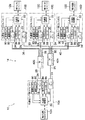
図1には本実施の形態に係る電子機器10が示されている。電子機器10は複数の電子回路12A,12B,12C,12Dを含んで構成されている。電子回路12A〜12Dのうち、電子回路12Aは他の電子回路12B〜12Dの動作制御等を行うマスタとして機能し、電子回路12B〜12Dは電子回路12Aの制御下で動作するスレーブとして機能する。
Hereinafter, an example of an embodiment of the present invention will be described in detail with reference to the drawings.
[Configuration of electronic equipment]
FIG. 1 shows an
なお、電子機器10としては任意の機器を適用可能であるが、一例としてLAN等のネットワークを介して画像データを受信し、受信した画像データに基づきスクリーン処理等の画像処理を行うことで各色成分(例えばC(シアン),M(マゼンダ),Y(イエロー),K(黒),S(特別色)等)の露光用画像データを生成し、生成した露光用画像データに基づいて各色成分毎に設けられたROS(Raster Output Scanner)による画像露光を制御することで各色成分の静電潜像を形成し、形成した各色成分の静電潜像を各色成分の現像剤で現像して重ね合わせることでフルカラーのトナー像を形成し、形成したフルカラーのトナー像を記録用紙に転写して定着させる構成のフルカラープリンタを適用することができる。
Although any device can be applied as the
この場合、スレーブとして機能する電子回路12B〜12Dとしては、各色成分の露光用画像データの生成及びROSによる画像露光を制御する画像処理回路を、マスタとして機能する電子回路12Aとしては、各画像処理回路の動作を制御する制御回路(例えばCPU及びメモリ等の周辺デバイスを含んで構成された制御回路)を適用することができる。 In this case, as the electronic circuits 12B to 12D functioning as slaves, an image processing circuit for controlling generation of image data for exposure of each color component and image exposure by ROS is used. As an electronic circuit 12A functioning as a master, each image processing is performed. A control circuit that controls the operation of the circuit (for example, a control circuit including a peripheral device such as a CPU and a memory) can be applied.
本実施の形態では、電子回路12Aと電子回路12B〜12Dの間の通信が光通信によって行われ、電子回路12Aと電子回路12B〜12Dの間には、これらの電子回路の間の光通信を実現する光通信システム14が設けられている。光通信システム14は、個々の電子回路12A〜12Dに接続された光通信インタフェース(I/F)部16A〜16Dを含んで構成されている。
In this embodiment, communication between the electronic circuit 12A and the electronic circuits 12B to 12D is performed by optical communication, and optical communication between these electronic circuits is performed between the electronic circuit 12A and the electronic circuits 12B to 12D. An
光通信I/F部16A〜16Dは接続されている電子回路12A〜12Dと同一の基板に各々搭載されている。光通信I/F部16A〜16Dは互いに略同一の構成とされており、複数個(例えば5個)のLD(レーザダイオード)が一列に配列されて成るLDアレイ18と、複数個(例えば5個)のPD(光検出器)が一列に配列されて成るPDアレイ20と、電子回路12、LDアレイ18及びPDアレイ20と各々接続された光通信制御部22が設けられている。
The optical communication I /
LDアレイ18の近傍には、LDアレイ18の環境湿度を計測する湿度センサ80、LDアレイ18の環境温度を計測する温度センサ82、LDアレイ18を冷却するための空冷ファン84、及びLDアレイ18を加熱するためのヒータ86が配置されている。
In the vicinity of the
個々の光通信I/F部16のLDアレイ18及びPDアレイ20は、各々光コネクタ24を着脱自在に構成されており、光通信I/F部16AのLDアレイ18に接続された光コネクタ24には第1光ファイバ26の一端が、PDアレイ20に装着された光コネクタ24には第1光ファイバ28の一端が取付けられており、光通信I/F部16BのLDアレイ18に接続された光コネクタ24には第2光ファイバ36の一端が、PDアレイ20に装着された光コネクタ24には第2光ファイバ30の一端が取付けられている。
Each of the
同様に、光通信I/F部16CのLDアレイ18に接続された光コネクタ24には第2光ファイバ38の一端が、PDアレイ20に接続された光コネクタ24には第2光ファイバ32の一端が取付けられており、光通信I/F部16DのLDアレイ18に接続された光コネクタ24には第2光ファイバ40の一端が、PDアレイ20に接続された光コネクタ24には第2光ファイバ34の一端が取付けられている。
Similarly, one end of the second
第1光ファイバ26,28、第2光ファイバ30,32,34,36,38,40は、POF(Plastic Optical Fiber)と称する合成樹脂製の光ファイバ(コア材がアクリル、コア材を覆うクラッド材がフッ素樹脂で形成された光ファイバ)が、LDアレイ18におけるLDの数及びPDアレイ20におけるPDの数と同数(例えば5本)だけ束ねられて各々構成されている。
The first
図2にも示すように、第1光ファイバ26、第2光ファイバ30,32,34の他端には光コネクタ24が各々取付けられ、これらの光コネクタ24は光シートバス42Aに各々接続されている。また、詳細な図示は省略するが、第1光ファイバ28、第2光ファイバ36,38,40の他端にも光コネクタ24が各々取付けられ、これらの光コネクタ24は光シートバス42Bに各々接続されている。なお、光シートバス42A,42Bは本発明に係る分配型光信号伝送体に対応している。
As shown in FIG. 2,
光シートバス42A,42Bは、合成樹脂製のベース部材に、図3に示す導波路部材44が光ファイバの本数と同数(例えば5個)だけ埋設されて構成されている。導波路部材44は、光透過率が高く後述するクラッド層よりも屈折率の高い材料(例えばポリメチルメタクリレート等)から成り、全体としては細長い矩形状で、幅寸法が階段状に変化している階段状部46A,46Bが中間部の2箇所に各々形成された形状とされている。
The
導波路部材44の両端部及び階段状部46A,46Bの計4箇所には、導波路部材44の長手方向及び上下方向(図3の上下方向)に対して45°の角度で傾斜された傾斜面44A〜44Dが各々形成されている。この傾斜面44A〜44Dは信号光入出射部として機能する。
Inclinations that are inclined at an angle of 45 ° with respect to the longitudinal direction and the vertical direction of the waveguide member 44 (vertical direction in FIG. 3) at both ends of the
導波路部材44は、導波路部材44の上面のうち個々の傾斜面44A〜44Dに対応する部分がベース部材の上面から各々露出するように埋設されており、光コネクタ24は導波路部材44のうち上記の露出部分と対向するようにベース部材に接続される。また、導波路部材44は、ベース部材の上面から露出している部分以外の外面が、導波路部材44を構成する材料よりも屈折率の低い材料(例えばフッ素ポリマ等)から成るクラッド層で被覆されている。
The
光シートバス42Aにおいて、第1光ファイバ26が取付けられた光コネクタ24は、導波路部材44のうち幅寸法が最大の部分に形成された傾斜面44Aに対応する露出部分と対向するようにベース部材に接続され、第2光ファイバ30,32,34が取付けられた光コネクタ24は、傾斜面44B〜44Dに対応する露出部分と対向するようにベース部材に接続される。
In the
第1光ファイバ26は光コネクタ24を介して光通信I/F部16AのLDアレイ18と接続されているので、光通信I/F部16AのLDアレイ18が発光すると、LDアレイ18の個々のLDから射出された信号光(レーザ光)は第1光ファイバ26を伝送して導波路部材44に入射し、傾斜面44Aで反射されることで導波路部材44内に閉じこめられた状態で導波路部材44内を拡散・伝播する。
Since the first
そして、図3(A)にも示すように、傾斜面44B〜44Dで各々反射されることで導波路部材44から射出し、光コネクタ24を介して第2光ファイバ30,32,34を伝送し光通信I/F部16B〜16DのPDアレイ20で各々受光される。
As shown in FIG. 3A, the light is emitted from the
また、光シートバス42Bにおいて、第1光ファイバ28が取付けられた光コネクタ24は傾斜面44Aに対応する露出部分と対向するようにベース部材に接続され、第2光ファイバ36,38,40が取付けられた光コネクタ24は、傾斜面44B〜44Dに対応する露出部分と対向するようにベース部材に接続される。
In the optical sheet bus 42B, the
第2光ファイバ36,38,40は光コネクタ24を介して光通信I/F部16B〜16DのLDアレイ18と接続されているので、光通信I/F部16B〜16Dの何れかのLDアレイ18が発光すると、該LDアレイ18の個々のLDから射出された信号光(レーザ光)は第2光ファイバ36,38,40の何れかを伝送して導波路部材44に入射し、傾斜面44B〜44Dの何れかで反射されることで導波路部材44内に閉じこめられた状態で導波路部材44内を拡散・伝播する。
Since the second
そして、図3(B)にも示すように、傾斜面44Aで反射されることで導波路部材44から射出し、光コネクタ24を介して第1光ファイバ28を伝送し、光通信I/F部16AのPDアレイ20で受光される。
Then, as shown in FIG. 3B, the light is emitted from the
このように、光通信I/F部16AのLDアレイ18は、第1光ファイバ26、光シートバス42A及び第2光ファイバ30,32,34を介して、光通信I/F部16B〜16DのPDアレイ20と光学的に各々結合されており、光通信I/F部16B〜16DのLDアレイ18は、第2光ファイバ36,38,40、光シートバス42B及び第1光ファイバ28を介して、光通信I/F部16AのPDアレイ20と光学的に各々結合されている。なお、光通信I/F部16Aと光通信I/F部16B〜16Dの間の光伝送路の距離は、本実施の形態では5m程度とされている。
As described above, the
次に、図4を参照し、光通信I/F部16A〜16Dに各々設けられた光通信制御部22の構成を説明する。光通信制御部22は、電子回路12に接続され電子回路12との通信を司る電子回路I/F部50を備えている。電子回路I/F部50は、他の電子回路12へ送信すべき情報を電子回路12から受信すると共に、他の電子回路12から受信した情報を電子回路12へ送信する。
Next, the configuration of the optical
電子回路I/F部50には送信制御部52が接続されており、電子回路12から電子回路I/F部50が受信した情報(他の電子回路12へ送信すべき送信情報)は送信制御部52へ出力される。送信制御部52はフラッシュメモリ等から成る不揮発性のNVMメモリ54を内蔵しており、このNVMメモリ54には最適発光強度テーブル(詳細は後述)が記憶される。
A
なお、本実施の形態において、光通信I/F部16AのNVMメモリ54には、スレーブとして機能する個々の電子回路12(12B〜12D)に接続された光通信I/F部16(16B〜16D)の数、及び、該光通信I/F部16(16B〜16D)に対して予め設定されたIDが予め記憶されており、光通信I/F部16B〜16DのNVMメモリ54には自身のID及び光通信I/F部16Aに対して予め設定されたIDが予め記憶されている。
In the present embodiment, the
上記情報は、例えばスレーブとして機能する電子回路12の増設等の電子機器10の構成変更に伴い、スレーブとして機能する電子回路12に接続された光通信I/F部16の数の増減があった場合に、オペレータ等によって書き替えられる。
In the above information, for example, the number of optical communication I / F units 16 connected to the
送信制御部52には8B/10Bエンコーダ56が接続されており、送信情報は送信制御部52から1バイトずつ8B/10Bエンコーダ56へ出力される。PDアレイ20の各PDは光を受光していない状態が継続するとレスポンスが低下するという特性を有している。
An 8B /
本実施の形態に係る光通信システム14は送信情報を光信号によってシリアルで送信するが、通常のデータには全ビットが0又は1のデータ(全ビットのデータを送信している間LDが発光しないデータ)が含まれている可能性があるので、このようなデータをシリアルで送信している間に、受信側のPDが非活性の状態となってレスポンスが低下する恐れがある。
The
このため、8B/10Bエンコーダ56は、送信制御部52から1バイト(8ビット)ずつ入力される送信情報を、全ビットに含まれる0のビット及び1のビットの割合が一定値以下にならないように予め設定された変換条件に従い、8ビットの送信情報を10ビットの送信情報へ変換する。なお、8B/10Bエンコーダ56は実際には複数設けられており、8ビットの送信情報から10ビットの送信情報への変換は個々の8B/10Bエンコーダ56で並列に行われる。
For this reason, the 8B /
8B/10Bエンコーダ56はP/S(パラレル/シリアル)変換部60を介してLD駆動部62に接続されており、8B/10Bエンコーダ56で変換された10ビットの送信情報は、P/S変換部60に入力されてシリアルのデータへ変換された後にLD駆動部62に入力される。
The 8B /
また、8B/10Bエンコーダ56にはECC(Error-Correcting Code)生成部58が接続されており、8B/10Bエンコーダ56から出力された10ビットの送信情報はECC生成部58にも入力され、ECC生成部58によって誤り訂正のためのエラーコレクションコードが生成される。ECC生成部58もP/S変換部60を介してLD駆動部62に接続されており、ECC生成部58で生成されたエラーコレクションコードは、P/S変換部60でシリアルのデータへ変換された後にLD駆動部62に入力される。
Further, an ECC (Error-Correcting Code)
そしてLD駆動部62は、8B/10Bエンコーダ56からP/S変換部60を介して入力された送信情報及びECC生成部58からP/S変換部60を介して入力されたエラーコレクションコードに応じてLDアレイ18の個々のLDの点消灯を制御することで、送信情報を光信号として送信する。
Then, the
また、LD駆動部62は送信制御部52と接続されており、送信制御部52からクロック信号及び発光強度制御情報が各々入力される。LDアレイ18のうちの特定のLDはクロック信号送信用とされており、LD駆動部62は入力されたクロック信号に従って特定のLDの点消灯を制御する。また、LD駆動部62はLDアレイ18の個々のLDの発光強度を制御可能とされており、入力された発光強度制御情報に従って個々のLDの発光強度を制御する。
The
湿度センサ80及び温度センサ82は送信制御部52と接続されており、湿度センサ80及び温度センサ82の各々から出力されたセンサ信号は送信制御部52に各々入力される。また、空冷ファン84及びヒータ86は送信制御部52と接続されており、送信制御部52から出力された駆動信号が、空冷ファン84及びヒータ86の各々に入力される。
The
一方、PDアレイ20には信号処理部64が接続されており、PDアレイ20の個々のPDが光信号を受信(受光)することで個々のPDから出力信号は、信号処理部64によって増幅され、デジタルの受信情報に復調されて出力される。信号処理部64はS/P(シリアル/パラレル)変換部66を介して誤り訂正部70に接続されており、信号処理部64から出力されたシリアルの受信情報はS/P変換部66によってパラレルの受信情報へ変換された後に誤り訂正部70に入力される。
On the other hand, a
また、信号処理部64はS/P変換部66を介して誤り検出部68に接続されている。誤り検出部68は、信号処理部64からS/P変換部66を介して入力されるパラレルの受信情報に含まれるエラーコレクションコードに基づき、受信情報本体にビット化け等の誤り(エラー)が生じていないか否かを検証する。誤り訂正部70は誤り検出部68に接続されており、受信情報本体に誤りが生じていることが誤り検出部68によって検出された場合に受信情報本体の誤り訂正を行う。
The
誤り訂正部70は8B/10Bデコーダ72を介して受信制御部74に接続されており、誤り訂正を経て誤り訂正部70から出力された受信情報(本体)は、8B/10Bデコーダ72により10ビット単位で通常の8ビットのデータに変換され、受信制御部74へ入力される。また、信号処理部64は受信制御部74と接続されており、受信した光信号のうちクロック信号は受信制御部74に直接入力され、光信号送信側との同期をとるために用いられる。
The
受信制御部74は電子回路I/F部50及び送信制御部52に各々接続されており、入力された受信情報を送信制御部52へ出力すると共に、電子回路I/F部50を介して電子回路12へ出力する。また、信号処理部64は送信制御部52にも接続されており、光信号受信(受光)時に光信号の受光量を表す受光量情報を送信制御部52へ出力する。
The
なお、光通信I/F部16Aは本発明に係る光通信装置、第1装置に対応しており、光通信I/F部16AのLDアレイ18の各LDは本発明に係る第1発光素子に、光通信I/F部16AのPDアレイ20の各PDは本発明に係る第1受光素子に各々対応している。また、光通信I/F部16B〜16Dは本発明に係る光通信装置、第2装置に対応しており、光通信I/F部16B〜16DのLDアレイ18の各LDは本発明に係る第2発光素子に、光通信I/F部16B〜16DのPDアレイ20の各PDは本発明に係る第2受光素子に各々対応している。
The optical communication I /
[電子機器の動作]
次に、本実施の形態に係る電子機器10の動作について説明する。
[Operation of electronic equipment]
Next, the operation of
本実施の形態では、電子機器10の電源投入時に、マスタとして機能する電子回路12Aに接続された光通信I/F部16Aの光通信制御部22(の送信制御部52)により、スレーブとして機能する各電子回路12に接続された光通信I/F部16へ情報を送信する際の光通信I/F部16AのLDアレイ18の各LDの最適発光強度を、個々の光通信I/F部16B〜16Cについて各々検出する最適発光強度検出処理(図5(A))が実行される。
In the present embodiment, when the
なお、送信制御部52は、最適発光強度検出処理の実行が終了すると、実行終了時点からの経過時間の計測を開始し、前回実行してから所定時間以上経過した場合にも、最適発光強度検出処理を行う。
When the execution of the optimum emission intensity detection process is completed, the
また、以下では光通信I/F部16Aを単に「マスタ」と称する。マスタで実行される最適発光強度検出処理は、本発明に係る第1検出手段に相当する処理であり、マスタの光通信制御部22の送信制御部52はこの最適発光強度検出処理を実行することで、本発明に係る第1検出手段として機能する。
Hereinafter, the optical communication I /
(マスタで実行される最適発光強度検出処理)
次に、図5を参照して、マスタでの最適発光強度検出処理の処理ルーチンについて説明する。
(Optimum emission intensity detection process executed by the master)
Next, with reference to FIG. 5, the processing routine of the optimum light emission intensity detection process at the master will be described.
まず、ステップ100において、NVMメモリ54を参照することで、スレーブとして機能する個々の電子回路12に接続された光通信I/F部16(以下、単に「スレーブ」と称する)の数及び個々のスレーブに予め設定されたIDを認識する。次のステップ102では、以下で処理対象とするスレーブ(便宜上、このスレーブを「スレーブn」と称する)を決定する。
First, in
ステップ104では、スレーブnに対するマスタのLDアレイ18の最適発光強度が、NVMメモリ54の最適発光強度テーブルに登録されているか否か判定する。判定が否定された場合には、例えばスレーブnが今回新たに増設された等の理由で、スレーブnに対するマスタのLDアレイ18の最適発光強度の検出が行われていないと判断できるので、ステップ106へ移行し、初期設定処理を行い、ステップ104で判定が肯定された場合にはステップ108へ移行し、通常設定処理を行う。
In
次のステップ110では、スレーブnに対して上記の最適発光強度を通知する情報を生成し、生成した情報に送信先IDとしてスレーブnのIDを、送信元IDとして自身(マスタ)のIDを各々付加して光通信により送信する。また、マスタで実行されている最適発光強度検出処理では、次のステップ112において、上述したステップ102以降の処理を全てのスレーブに対して行ったか否か判定する。
In the
判定が肯定された場合は処理ルーチンを終了し、判定が否定された場合はステップ102に戻り、新たなスレーブを処理対象としてステップ102の処理を繰り返す。これにより、全てのスレーブに対してマスタのLDアレイ18の最適発光強度が各々検出され、検出された最適発光強度がNVMメモリ54の最適発光強度テーブルに各々登録されると共に、対応するスレーブnに通知されることになる。
If the determination is affirmative, the processing routine is terminated. If the determination is negative, the processing returns to step 102, and the processing of
次に、図6に示す初期設定処理の処理ルーチンについて説明する。 Next, the processing routine of the initial setting process shown in FIG. 6 will be described.
初期設定処理では、ステップ200でスレーブnに対するマスタのLDアレイ18の最適発光強度を検出するためのLDアレイ18の各LDの発光強度の初期値及び変更範囲として所定値を設定した後に、ステップ202へ移行する。次のステップ202では、最適発光強度検出のためにLDアレイ18の各LDを発光させる際に用いる強度検出用情報に、送信先IDとしてスレーブnのIDを、送信元IDとして自身(マスタ)のIDを各々付加すると共に、LDアレイ18の各LDの発光強度(最初は上記で設定した初期値)を表す発光強度情報を付加する。
In the initial setting process, after setting a predetermined value as the initial value and change range of the light emission intensity of each LD of the
そしてステップ204では、設定した発光強度でLDアレイ18の各LDを発光させるための発光強度制御情報をLD駆動部62へ出力すると共に、スレーブn及びマスタのID、発光強度情報を付加した強度検出用情報(送信情報)を8B/10Bエンコーダ56、ECC生成部58、P/S変換部60を介してLD駆動部62へ出力する。
In
これにより、点灯(発光)時の発光強度が設定した発光強度に一致するように、送信情報に応じてマスタのLDアレイ18の各LDが点消灯されることで、上記の送信情報に応じて変調された光信号がマスタのLDアレイ18から射出され、第1光ファイバ26、光シートバス42A、第2光ファイバ30,32,34を伝送した後に各スレーブ(光通信I/F部16B〜16D)のPDアレイ20で各々受光されることになる。
Thereby, each LD of the
なお、スレーブへ送信する情報に、スレーブのIDを送信先IDとして付加することにより、特定のスレーブへ送信した情報が、特定のスレーブ以外のスレーブで自装置宛の情報と誤認識されることを防止することができる。 By adding the slave ID as the transmission destination ID to the information transmitted to the slave, the information transmitted to the specific slave is misrecognized as information addressed to the own device by a slave other than the specific slave. Can be prevented.
一方、各スレーブでは、PDアレイ20が光信号を受光し、その受光量がPDアレイ20の各PDの許容範囲内であった場合には、受光された光信号が受信情報として復調され、S/P変換部66、誤り検出部68、誤り訂正部70、8B/10Bデコーダ72を介して受信制御部74へ入力される。そして、受信情報が受信制御部74から送信制御部52へ入力されることで、送信制御部52において後述する光信号受信時処理(図9参照)が実行される。
On the other hand, in each slave, when the
次のステップ206では、スレーブnから受光状態通知を受信したか否か判定する。判定が否定された場合はステップ208へ移行し、光信号を送信してから所定時間が経過したか否か判定する。判定が否定された場合はステップ206に戻り、何れかの判定が肯定される迄、ステップ206,208を繰り返す。
In the
ここで、スレーブnにおける光信号の受光量がPDアレイ20の各PDの許容範囲外であった場合(受光量が不足していた場合)には、ステップ208の判定が肯定されてステップ210へ移行し、発光強度の設定値を所定量だけ増加設定した後にステップ202に戻る。これにより、点灯(発光)時の発光強度が所定量だけ増加するように送信情報に応じてLDアレイ18の各LDが再度点消灯されることで、同一の送信情報に応じて変調された光信号が各スレーブへ再度送信される。
Here, when the received light amount of the optical signal in the slave n is outside the allowable range of each PD of the PD array 20 (when the received light amount is insufficient), the determination in
また、前述のステップ210の処理は、ステップ208の判定が肯定される毎に実行される。従って、スレーブnにおける光信号の受光量が不足していた場合には、スレーブnにおける光信号の受光量が許容範囲内になるまで、マスタのLDアレイ18の各LDの発光強度を所定量ずつ増大させながら光信号の送信が繰り返されることになる。
Further, the process of
一方、スレーブnから発光強度情報を付加した受光状態情報を受信すると、ステップ206での判定が肯定されてステップ212へ移行し、受信した受光状態情報を参照することで、該受光状態情報に付加されている発光強度情報が表す発光強度が、スレーブnへ情報を送信する際のLDアレイ18の各LDの最適発光強度か否か判定する。
On the other hand, when the light reception state information to which the light emission intensity information is added is received from the slave n, the determination in
この最適発光強度としては、例えばスレーブnのPDアレイ20の各PDの受光量が受光量の許容範囲の下限値に一致する最適状態となる発光強度を適用することができる。最適発光強度で発光させることで、マスタのLDアレイ18を最大限に長寿命化できると共に、発熱量を必要最小限に抑制できる。
As this optimum light emission intensity, for example, a light emission intensity that is in an optimal state in which the light reception amount of each PD of the slave
また、受信した受光状態情報が表す受光量が上記の最適状態に相当する受光量と相違していた場合には、ステップ212の判定が否定されてステップ214へ移行し、受光状態情報によって通知されたスレーブnのPDアレイ20の各PDの受光状態に応じて発光強度を変更設定した後にステップ202に戻る。
If the received light amount indicated by the received light reception state information is different from the light reception amount corresponding to the optimum state, the determination in
これにより、点灯(発光)時の発光強度が変更設定後の発光強度に一致するように前回と同一の情報に応じてLDアレイ18の各LDが再度点消灯され、前回と同一の情報に応じて変調された光信号が前回とは異なる発光強度でスレーブnへ再度送信される。従って、スレーブnにおける光信号の受光量が最適状態に相当する受光量と相違していた場合には、スレーブnにおける光信号の受光量が最適状態になるように、スレーブnのPDアレイ20の各PDの受光状態に応じてマスタのLDアレイ18の各LDの発光強度を変更設定しながら光信号の送信が繰り返されることになる。
Thereby, each LD of the
スレーブnのPDアレイ20の各PDの受光量が最適状態に相当する受光量に一致すると、ステップ212の判定が肯定されてステップ216へ移行する。ステップ216では、湿度センサ80、温度センサ82からセンサ信号を取り込み、現在の発光強度(最後に受信した受光状態情報に付加されていた発光強度情報が表す発光強度)を、スレーブnに対するマスタのLDアレイ18の最適発光強度として、現在の環境温度、環境湿度、及びスレーブnのIDと対応付けてNVMメモリ54の最適発光強度テーブルに登録する。このように、マスタのNVMメモリ54は本発明に係る第1記憶手段に対応している。
When the received light amount of each PD in the
また、上記のように、処理対象のスレーブnへ送信する強度検出用情報に発光強度情報を付加し、スレーブnから受信した受光状態情報に付加されている発光強度情報に基づいて、最適発光強度(スレーブnにおける光信号の受光量が最適状態になるときのマスタのLDアレイ18の発光強度)を認識する処理を実施することにより、最適発光強度を確実に認識することができる。
Further, as described above, the emission intensity information is added to the intensity detection information transmitted to the slave n to be processed, and the optimum emission intensity is based on the emission intensity information added to the light reception state information received from the slave n. By executing the process of recognizing (the light emission intensity of the
次に、図7に示す通常設定処理の処理ルーチンについて説明する。 Next, the processing routine of the normal setting process shown in FIG. 7 will be described.
通常設定処理では、ステップ300で、前回の最適発光強度検出処理で検出されたスレーブnに対するマスタのLDアレイ18の最適発光強度を最適発光強度テーブルから読み出し、次のステップ302では、今回検出する最適発光強度が読み出した最適発光強度と同一又は近似した値となることを前提に、読み出した最適発光強度に基づいてLDアレイ18の各LDの発光強度の初期値及び変更範囲を設定する。
In the normal setting process, in
前回の最適発光強度検出処理で検出されたスレーブnに対するマスタのLDアレイ18の最適発光強度が最適発光強度テーブルに登録されていた場合、今回検出する最適発光強度は、最適発光強度テーブルに登録されている最適発光強度と同一又は近似した値となる可能性が高い。
When the optimum emission intensity of the
例えば、発光強度の変更範囲を、読み出した最適発光強度を中心としかつ通常よりも狭い範囲に設定し、発光強度の初期値を、設定した変更範囲の上限又は下限に相当する値に設定する。これにより、最適発光強度検出処理に要する時間を短縮することができる。 For example, the change range of the emission intensity is set to a range that is centered on the read optimum emission intensity and narrower than usual, and the initial value of the emission intensity is set to a value corresponding to the upper limit or lower limit of the set change range. Thereby, the time required for the optimum light emission intensity detection process can be shortened.
次のステップ304では、強度検出用情報に、送信先IDとしてスレーブnのIDを、送信元IDとして自身(マスタ)のIDを各々付加すると共に、LDアレイ18の各LDの発光強度を表す発光強度情報を付加する。そしてステップ306では、設定した発光強度でLDアレイ18の各LDを発光させるための発光強度制御情報をLD駆動部62へ出力する。
In the
次のステップ308では、スレーブnから受光状態通知を受信したか否か判定する。判定が否定された場合はステップ310へ移行し、空冷ファン84、ヒータ86を駆動して現在の環境条件を発光可能な環境条件に補正する環境補正処理を実行する。ここで環境条件の補正が行われなかった場合には、後述する通りフラグがセットされる。
In the
次のステップ312で、フラグがセットされているか否かを判定し、フラグがセットされていれば、ステップ312の判定が肯定されてステップ318へ移行し、発光強度の設定値を所定量だけ増加設定した後にステップ304に戻る。これにより、点灯(発光)時の発光強度が所定量だけ増加するように送信情報に応じてLDアレイ18の各LDが再度点消灯されることで、同一の送信情報に応じて変調された光信号が各スレーブへ再度送信される。
In the
フラグがセットされていない場合は、ステップ314でスレーブnから受光状態通知を受信したか否か判定する。判定が否定された場合はステップ316へ移行し、光信号を送信してから所定時間が経過したか否か判定する。判定が否定された場合はステップ314に戻り、何れかの判定が肯定される迄、ステップ314,316を繰り返す。
If the flag is not set, it is determined in
ステップ316の判定が肯定されてステップ318へ移行し、発光強度の設定値を所定量だけ増加設定した後にステップ304に戻る。これにより、点灯(発光)時の発光強度が所定量だけ増加するように送信情報に応じてLDアレイ18の各LDが再度点消灯されることで、同一の送信情報に応じて変調された光信号が各スレーブへ再度送信される。
The determination in
一方、スレーブnから発光強度情報を付加した受光状態情報を受信すると、ステップ308又はステップ314での判定が肯定されてステップ320へ移行し、受信した受光状態情報を参照することで、該受光状態情報に付加されている発光強度情報が表す発光強度が、スレーブnへ情報を送信する際のLDアレイ18の各LDの最適発光強度か否か判定する。受信した受光状態情報が表す受光量が上記の最適状態に相当する受光量と相違していた場合には、ステップ320の判定が否定されてステップ322へ移行し、受光状態情報によって通知されたスレーブnのPDアレイ20の各PDの受光状態に応じて発光強度を変更設定した後にステップ304に戻る。
On the other hand, when the light reception state information to which the light emission intensity information is added is received from the slave n, the determination in
スレーブnのPDアレイ20の各PDの受光量が最適状態に相当する受光量に一致すると、ステップ320の判定が肯定されてステップ324へ移行する。ステップ324では、湿度センサ80、温度センサ82からセンサ信号を取り込み、現在の発光強度をスレーブnに対するマスタのLDアレイ18の最適発光強度として、現在の環境温度、環境湿度、及びスレーブnのIDと対応付けてNVMメモリ54の最適発光強度テーブルに登録する。
When the received light amount of each PD in the
次に、図8に示す環境補正処理の処理ルーチンについて説明する。 Next, the processing routine of the environment correction process shown in FIG. 8 will be described.
環境補正処理では、ステップ400で湿度センサ80及び温度センサ82からセンサ信号を取り込んで、現在の環境温度、環境湿度を検出する。次のステップ402で、NVMメモリ54から、スレーブnに対するマスタのLDアレイ18に関し、設定された発光強度で登録された環境温度、環境湿度を最適発光強度テーブルから読み出し、ステップ404で、読み出した環境温度、環境湿度の各々の上限値及び下限値を設定する。上限値から下限値までの範囲が、設定された発光強度での環境温度、環境湿度の許容範囲である。
In the environmental correction process, in
例えば、下記表1に示すように、3回目の最適発光強度検出処理までは設定された発光強度(光量レベル3)で光通信が可能であり、即ち、スレーブnから受光状態通知を受信することができ、4回目の検出処理で設定された発光強度で光通信が不能となった場合には、3回目までの通信履歴から、環境温度の許容範囲は20℃〜50℃、環境湿度の許容範囲は40%〜70%となる。現在の環境温度は60℃、環境湿度は40%であるから、環境温度が許容範囲を超えている。なお、この例では、発光強度は10段階の光量レベルで変更可能である。 For example, as shown in Table 1 below, optical communication is possible with the set light emission intensity (light quantity level 3) until the third optimum light emission intensity detection process, that is, a light reception state notification is received from slave n. If the optical communication becomes impossible at the emission intensity set in the fourth detection process, the allowable temperature range is 20 ° C to 50 ° C and the allowable environmental humidity is based on the communication history up to the third time. The range is 40% to 70%. Since the current environmental temperature is 60 ° C. and the environmental humidity is 40%, the environmental temperature exceeds the allowable range. In this example, the light emission intensity can be changed at 10 light levels.

次のステップ406で、環境温度又は環境湿度が各々の許容範囲を超えているか否かを判定する。判定が否定された場合はステップ418へ移行し、フラグをセットする。判定が肯定された場合はステップ408でフラグをリセットし、そしてステップ410でLDアレイ18の各LDを冷却又は過熱するための駆動信号を、空冷ファン84又はヒータ86へ出力する。これにより、環境温度、環境湿度の何れかが上限値を超えた場合には、空冷ファン84が駆動されてLDアレイ18の各LDが冷却され、環境温度、環境湿度の何れかが下限値を超えた場合には、ヒータ86が駆動されてLDアレイ18の各LDが加熱される。
In the
次のステップ412で、空冷ファン84又はヒータ86を駆動してから所定時間が経過したか否か判定する。判定が否定された場合は、判定が肯定されるまでステップ412を繰り返す。判定が肯定された場合は、次のステップ414で、強度検出用情報にIDを付加すると共に、LDアレイ18の各LDの発光強度を表す発光強度情報を付加し、ステップ416で、設定した発光強度でLDアレイ18の各LDを発光させるための発光強度制御情報を、再度、LD駆動部62へ出力する。
In the
そして、同じ発光強度でスレーブnに光信号が再度送信される。スレーブnのPDアレイ20の各PDの受光量が最適状態に相当する受光量に一致すると、図7のステップ324で、湿度センサ80、温度センサ82からセンサ信号を取り込み、現在の発光強度をスレーブnに対するマスタのLDアレイ18の最適発光強度として、現在の環境温度、環境湿度、及びスレーブnのIDと対応付けてNVMメモリ54の最適発光強度テーブルに登録する。
Then, the optical signal is transmitted again to the slave n with the same emission intensity. When the received light amount of each PD in the
例えば、上記表1に示した例では、下記表2に示すように、空冷ファン84が駆動されてLDアレイ18の各LDが冷却され、環境温度が50℃と許容範囲内となって、設定された発光強度(光量レベル3)で光通信が可能となる。
For example, in the example shown in Table 1 above, as shown in Table 2 below, the
このように、環境補正処理を実行することで、環境条件の変化によりLDアレイ18の各LDの発光強度が低下した場合にも、発光強度の設定値を増加することなく光通信を行うことができる。また、マスタのLDアレイ18を最大限に長寿命化できると共に、発熱量を必要最小限に抑制することができる。
As described above, by executing the environment correction processing, optical communication can be performed without increasing the set value of the light emission intensity even when the light emission intensity of each LD of the
次に、図9を参照して、上述したマスタでの処理に応じて実施される、各スレーブでの光信号受信時処理の処理ルーチンについて説明する。 Next, with reference to FIG. 9, a processing routine of processing at the time of optical signal reception at each slave, which is performed according to the processing at the master described above, will be described.
上述した通り、マスタからの受信情報が受信制御部74から送信制御部52へ入力されることで、送信制御部52において光信号受信時処理が実行される。この光信号受信時処理では、まずステップ500において、受信情報に含まれている送信先IDを抽出し、抽出した送信先IDが自装置のIDか否かを判定することで、受信情報が自装置宛の情報か否か判定する。判定が否定された場合は何ら処理を行うことなく光信号受信時処理を終了する。また、判定が肯定された場合(自装置がスレーブnの場合)はステップ502へ移行し、ステップ502以降の処理を行う。
As described above, when the reception information from the master is input from the
また、スレーブnにおける光信号の受光量がPDアレイ20の各PDの許容範囲内であった場合には、送信制御部52で光信号受信時処理が実行されると共に、前述のステップ500の判定が肯定されてステップ502へ移行し、受信情報が強度検出用情報か否かを判断することで、自装置に対する最適発光強度の検出がマスタで実行中か否か判定する。判定が否定された場合はステップ508へ移行し、受信情報が最適発光強度を通知する情報か否かを判定する。この判定も否定された場合はステップ512へ移行し、受信情報の内容に応じた処理を実行して光信号受信時処理を終了する。
If the received light amount of the optical signal in the slave n is within the allowable range of each PD of the
また、ステップ502の判定が肯定された場合はステップ504へ移行し、信号処理部64から入力される受光量情報に基づいて、PDアレイ20の各PDによる光信号の受光状態を表す受光状態情報を生成する。
If the determination in
なお、受光状態情報としては、例えばPDアレイ20の各PDの受光量の許容範囲の下限値とPDアレイ20の各PDによる光信号の実際の受光量の偏差を表す情報を適用することができるが、これに代えて、PDアレイ20の各PDの受光量の許容範囲の上限値とPDアレイ20の各PDによる光信号の実際の受光量の偏差を表す情報を適用してもよいし、PDアレイ20の各PDの受光量の許容範囲の上限値及び下限値、PDアレイ20の各PDによる光信号の実際の受光量を各々表す情報を適用してもよい。
As the light reception state information, for example, information indicating a deviation between a lower limit value of a light reception amount of each PD of the
そしてステップ506では、受信情報から発光強度情報を抽出し、抽出した発光強度情報を生成した受光状態情報に付加すると共に、送信先IDとしてマスタのIDを、送信元IDとして自装置のIDを各々付加した後に、予め設定された発光強度(これに代えて前回検出した最適発光強度を適用してもよい)でLDアレイ18の各LDを発光させるための発光強度制御情報をLD駆動部62へ出力すると共に、発光強度情報を付加した受光状態情報を8B/10Bエンコーダ56、ECC生成部58、P/S変換部60を介してLD駆動部62へ出力し、光信号受信時処理を終了する。
In
これにより、点灯(発光)時の発光強度が設定した発光強度に一致するように、上記の受信状態情報に応じてスレーブnのLDアレイ18の各LDが点消灯されることで、上記の受信状態情報に応じて変調された光信号がスレーブnのLDアレイ18から射出され、第2光ファイバ36,38,40の何れか、光シートバス42B、第1光ファイバ28を伝送した後にマスタのPDアレイ20で受光されることになる。
Thereby, each LD of the
ステップ500の判定が肯定された後に、ステップ502の判定が否定され、ステップ508の判定が肯定されてステップ510へ移行し、マスタから通知されたスレーブnに対するマスタのLDアレイ18の最適発光強度がスレーブnのNVMメモリ54に記憶される。このように、各スレーブのNVMメモリ54は本発明に係る第2記憶手段に対応している。
After the determination in
マスタでの最適発光強度検出処理が終了すると、マスタの送信制御部52は、個々のスレーブに対し、マスタへ情報を送信する際の個々のスレーブのLDアレイ18の各LDの最適発光強度を検出する処理の実行を指示する所定の情報を、光通信によって順に送信する。これにより、前記所定の情報を受信することで最適発光強度を検出する処理の実行が指示されたスレーブ(便宜上「スレーブn」と称する)では、送信制御部52で最適発光強度検出処理が実行される。
When the optimum emission intensity detection process at the master is completed, the master
なお、スレーブで実行される最適発光強度検出処理は本発明に係る設定手段に相当する処理であり、スレーブの光通信制御部22の送信制御部52は、この最適発光強度検出処理を実行することで本発明に係る設定手段として機能する。
The optimum light emission intensity detection process executed by the slave is a process corresponding to the setting means according to the present invention, and the
(スレーブで実行される最適発光強度検出処理)
次に、図10を参照して、スレーブでの最適発光強度検出処理の処理ルーチンについて説明する。
(Optimal emission intensity detection process executed by the slave)
Next, with reference to FIG. 10, the processing routine of the optimum light emission intensity detection process in the slave will be described.
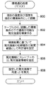
まず、ステップ600において、NVMメモリ54を参照することで、スレーブnのLDアレイ18の最適発光強度が、NVMメモリ54の最適発光強度テーブルに登録されているか否か判定する。判定が否定された場合には、ステップ602へ移行し、初期設定処理を行い、ステップ600で判定が肯定された場合にはステップ604へ移行し、通常設定処理を行う。これにより、スレーブのLDアレイ18の最適発光強度が各々検出され、検出された最適発光強度がNVMメモリ54の最適発光強度テーブルに各々登録されると共に、マスタに通知されることになる。
First, in
マスタの初期設定処理では、ステップ200でスレーブnに対するマスタのLDアレイ18の最適発光強度を検出するためのLDアレイ18の各LDの発光強度の初期値及び変更範囲として所定値を設定したが、スレーブの初期設定処理では、まずマスタから通知されてNVMメモリ54に記憶させた最適発光強度(スレーブnに対するマスタのLDアレイ18の最適発光強度)を読み出し、今回検出する最適発光強度がNVMメモリ54から読み出した最適発光強度(マスタで検出されて通知された、スレーブnに対するマスタのLDアレイ18の最適発光強度)と同一又は近似した値となることを前提に、読み出した最適発光強度に基づいてスレーブnのLDアレイ18の各LDの発光強度の初期値及び変更範囲を設定する。これにより、最適発光強度検出処理に要する時間を短縮することができる。
In the initial setting process of the master, a predetermined value is set as an initial value and a change range of the light emission intensity of each LD of the
スレーブの初期設定処理は、上記の点を除いて、図6に示すマスタの初期設定処理と同じ処理ルーチンであるため、同一部分については説明を省略する。また、スレーブの通常設定処理は、図7に示すスレーブの通常設定処理と同じ処理ルーチンであるため説明を省略する。 The initial setting process of the slave is the same processing routine as the initial setting process of the master shown in FIG. The slave normal setting process is the same processing routine as the slave normal setting process shown in FIG.
次に、図11を参照して、上述した各スレーブでの処理に応じて実施される、マスタでの光信号受信時処理の処理ルーチンについて説明する。 Next, with reference to FIG. 11, the processing routine of the optical signal reception process at the master, which is performed according to the above-described processing at each slave, will be described.
上述した通り、各スレーブからの受信情報が受信制御部74から送信制御部52へ入力されることで、送信制御部52において光信号受信時処理が実行される。この光信号受信時処理では、まずステップ700において、受信情報に含まれている送信先IDを抽出し、抽出した送信先IDが自装置のIDか否かを判定することで、受信情報が自装置宛の情報か否か判定する。判定が否定された場合は何ら処理を行うことなく光信号受信時処理を終了する。
As described above, the reception information from each slave is input from the
判定が肯定された場合はステップ702へ移行し、ステップ702以降の処理を行う。なお、本実施の形態の構成では、各スレーブが送信する情報は何れもマスタ宛の情報であり、ステップ700の判定が否定されることはないので、ステップ700を省略してもよい。
If the determination is affirmative, the routine proceeds to step 702, and the processing after
また、マスタにおける光信号の受光量がPDアレイ20の各PDの許容範囲内であった場合には、マスタの送信制御部52で光信号受信時処理が実行されると共に、ステップ700の判定が肯定されてステップ702へ移行し、受信情報が強度検出用情報か否かを判断することで、自装置に対する最適発光強度の検出がスレーブnで実行中か否か判定する。判定が否定された場合はステップ710へ移行し、受信情報の内容に応じた処理を実行して光信号受信時処理を終了する。
When the received light amount of the optical signal in the master is within the allowable range of each PD of the
また、ステップ702の判定が肯定された場合はステップ704へ移行し、信号処理部64から入力される受光量情報に基づいて、PDアレイ20の各PDによる光信号の受光状態を表す受光状態情報を生成する。
If the determination in
そしてステップ706では、受信情報から発光強度情報を抽出し、ステップ708で、抽出した発光強度情報を生成した受光状態情報に付加すると共に、送信先IDとしてスレーブnのIDを、送信元IDとして自装置(マスタ)のIDを各々付加した後に、先に検出して最適発光強度テーブルに登録されているスレーブnに対する最適発光強度でLDアレイ18の各LDを発光させるための発光強度制御情報をLD駆動部62へ出力する。
In
また、発光強度情報を付加した受光状態情報(送信情報)を8B/10Bエンコーダ56、ECC生成部58、P/S変換部60を介してLD駆動部62へ出力し、光信号受信時処理を終了する。これにより、スレーブn及びマスタのID、発光強度情報が付加された受光状態情報が、マスタから光通信によってスレーブnへ送信される。
In addition, the light reception state information (transmission information) to which the light emission intensity information is added is output to the
以上説明した通り、本実施の形態では、マスタ及び各スレーブで光通信の相手に対する最適発光強度の検出が完了すると、通常の光通信が行われるが、この通常の光通信において、マスタが任意のスレーブに情報を送信する場合、マスタの送信制御部52は、情報送信対象のスレーブのIDと対応付けてNVMメモリ54の最適発光強度テーブルに登録されている最適発光強度を読み出し、読み出した最適発光強度でLDアレイ18の各LDを発光させるための発光強度制御情報をLD駆動部62へ出力する。
As described above, in the present embodiment, when the detection of the optimum light emission intensity for the optical communication partner is completed in the master and each slave, normal optical communication is performed. When transmitting information to the slave, the master
この処理は本発明に係る第1制御手段に対応しており、この処理を実行することでマスタの送信制御部52は本発明に係る第1制御手段として機能する。これにより、マスタから任意のスレーブへの情報の送信に際し、情報送信先のスレーブにおける光信号の受光量が最適状態になるように、マスタのLDアレイ18の各LDの発光強度が制御される。
This process corresponds to the first control means according to the present invention, and by executing this process, the master
また、任意のスレーブ(スレーブn)がマスタに情報を送信する場合、スレーブnの送信制御部52は、NVMメモリ54に記憶されている最適発光強度(マスタに対するスレーブnのLD18の最適発光強度)を読み出し、読み出した最適発光強度でLDアレイ18の各LDを発光させるための発光強度制御情報をLD駆動部62へ出力する。
When an arbitrary slave (slave n) transmits information to the master, the
これにより、任意のスレーブnからマスタへの情報の送信に際しても、マスタにおける光信号の受光量が最適状態になるように、スレーブnのLDアレイ18の各LDの発光強度が制御される。この処理は本発明に係る第2制御手段に対応しており、この処理を実行することでスレーブの送信制御部52は本発明に係る第2制御手段として機能する。これにより、任意のスレーブからマスタへの情報の送信に際し、情報送信先のマスタにおける光信号の受光量が最適状態になるように、スレーブのLDアレイ18の各LDの発光強度が制御される。
As a result, even when information is transmitted from any slave n to the master, the light emission intensity of each LD of the
このように、本実施の形態では、各スレーブに対するマスタのLDアレイ18の最適発光強度がマスタによって検出され、マスタは任意のスレーブへ情報を送信する際にLDアレイ18の各LDの発光強度が情報送信先のスレーブに対応する最適発光強度となるように制御するので、光通信によって個々のスレーブへ確実に情報を送信することができると共に、LDアレイ18の発光強度が個々のスレーブ毎に最適化されるので、マスタのLDアレイ18が必要以上の発光強度で発光されることでLDアレイ18の寿命に悪影響を及ぼしたり、LDアレイ18が必要以上に発熱することを防止することができる。
Thus, in the present embodiment, the optimum light emission intensity of the
特に、本実施の形態では、マスタ及び各スレーブで最適発光強度を検出する際に、現在の環境条件を発光可能な環境条件に補正する「環境補正処理」を実行するので、環境条件の変化によりLDアレイ18の各LDの発光強度が低下した場合にも、最適発光強度の設定値を増加することなく光通信を行うことができる。また、最適発光強度の設定値を増加しないので、LDアレイ18を最大限に長寿命化できると共に、LDアレイ18の発熱量を必要最小限に抑制することができる。
In particular, in the present embodiment, when the optimum light emission intensity is detected by the master and each slave, an “environment correction process” for correcting the current environmental condition to an environmental condition capable of emitting light is executed. Even when the light emission intensity of each LD of the
[環境適応処理]
なお、上記の実施の形態では、通常設定処理で通信相手から受光状態が通知されない場合に、現在の環境条件を発光可能な環境条件に補正する「環境補正処理」を実施する例について説明したが、「環境補正処理」を実施する代わりに、現在の環境条件で発光可能な発光強度を設定する「環境適応処理」を実施することもできる。
[Environmental adaptation processing]
In the above embodiment, an example has been described in which the “environment correction process” is performed to correct the current environmental condition to the environmental condition capable of emitting light when the light receiving state is not notified from the communication partner in the normal setting process. Instead of performing the “environment correction process”, an “environment adaptation process” for setting the light emission intensity that can be emitted under the current environmental conditions can be performed.
次に、図12を参照して、環境適応処理の処理ルーチンについて説明する。 Next, a processing routine for environment adaptation processing will be described with reference to FIG.
環境適応処理では、ステップ800で湿度センサ80及び温度センサ82からセンサ信号を取り込んで、現在の環境温度T、環境湿度Wを、現在の環境条件として検出する。次のステップ802で、NVMメモリ54から、スレーブnに対するマスタのLDアレイ18に関し、現在の環境温度、環境湿度で登録された発光強度を最適発光強度テーブルから検索する。ステップ804で、今回検出する最適発光強度が検索された発光強度と同一又は近似した値となることを前提に、検索された発光強度に基づいてLDアレイ18の各LDの発光強度の初期値及び変更範囲を設定する。
In the environmental adaptation processing, sensor signals are taken from the
次のステップ806で、強度検出用情報にIDを付加すると共に、LDアレイ18の各LDの発光強度を表す発光強度情報を付加し、ステップ808で、設定した発光強度でLDアレイ18の各LDを発光させるための発光強度制御情報を、再度、LD駆動部62へ出力する。
In the
このように、環境適応処理を実行することで、環境条件の変化によりLDアレイ18の各LDの発光強度が低下した場合にも、通信履歴を検索することで環境条件に応じた最適発光強度を設定することができ、設定された最適発光強度で光通信を行うことができる。
As described above, by executing the environment adaptation processing, even when the light emission intensity of each LD of the
10 電子機器
12 電子回路
14 光通信システム
16 光通信I/F部
18 LDアレイ
20 PDアレイ
22 光通信制御部
26 光ファイバ
28 光ファイバ
30 光ファイバ
32 光ファイバ
34 光ファイバ
36 光ファイバ
38 光ファイバ
40 光ファイバ
42 光シートバス
52 送信制御部
54 NVMメモリ
80 湿度センサ
82 温度センサ
84 空冷ファン
86 ヒータ
DESCRIPTION OF
Claims (4)
発光強度制御情報に基づいて前記発光素子を駆動する発光素子駆動部と、
前記受光素子が受信した光信号から通信した機器の受信状態を含む受信情報を取得する受信情報取得部と、
前記発光素子が置かれた環境温度及び環境湿度を計測する計測手段と、
環境温度及び環境湿度を調整する加熱手段及び冷却手段の少なくとも一方を駆動して、前記発光素子が置かれた環境温度及び環境湿度の少なくとも一方を補正する補正手段と、
接続された複数の機器毎に、前記発光素子の発光強度の設定値と、当該発光強度の設定値で発光したときの前記計測手段で計測された環境温度及び環境湿度と、当該発光強度の設定値で発光したときの前記受信情報取得部で取得された受信情報又は当該受信情報取得の有無と、を関連付けて、前記発光素子を最適な発光強度で発光させるための最適発光強度情報を含む発光強度制御情報として記憶した記憶手段と、
前記発光強度制御情報に基づいて前記発光素子駆動部により前記発光素子を駆動して前記複数の機器毎に最適発光強度情報を含む強度検出用の光信号を送信し、
前記受信情報取得部で受信情報を取得できない場合には、
環境温度及び環境湿度の少なくとも一方が上限値を超えると前記冷却手段が駆動されて前記発光素子が冷却されると共に、環境温度及び環境湿度の少なくとも一方が下限値を下回ると前記加熱手段が駆動されて前記発光素子が加熱されるように前記補正手段により環境温度及び環境湿度の少なくとも一方を補正した後に前記発光強度制御情報に基づいて前記強度検出用の光信号を再度送信するか、又は前記計測手段で計測された環境温度及び環境湿度に応じて前記発光強度の設定値を変更して変更後の最適発光強度情報を含む強度検出用の光信号を再度送信し、
前記受信情報取得部で受信情報を取得できた場合には、取得された受信情報に基づいて新たな発光強度制御情報を検出して前記記憶手段に記憶するように制御する制御手段と、
を備えた光通信装置。 Optical communication that includes a light-emitting element that transmits optical signals and a light-receiving element that receives optical signals, is connected to multiple devices via a distributed optical signal transmitter, and can transmit and receive optical signals to and from multiple devices A device,
A light emitting element driving unit that drives the light emitting element based on light emission intensity control information;
A reception information acquisition unit that acquires reception information including a reception state of a device that communicates from an optical signal received by the light receiving element;
Measuring means for measuring the environmental temperature and the environmental humidity where the light emitting element is placed;
A correction unit that drives at least one of a heating unit and a cooling unit that adjust the environmental temperature and the environmental humidity, and corrects at least one of the environmental temperature and the environmental humidity where the light emitting element is placed;
For each of a plurality of connected devices, a setting value of the light emission intensity of the light emitting element, an environmental temperature and an environmental humidity measured by the measuring means when light is emitted with the setting value of the light emission intensity, and a setting of the light emission intensity Light emission including optimum light emission intensity information for causing the light emitting element to emit light at an optimum light emission intensity by associating the reception information acquired by the reception information acquisition unit when emitting light with a value or the presence or absence of acquisition of the reception information. Storage means stored as intensity control information;
Based on the light emission intensity control information, the light emitting element driving unit drives the light emitting element to transmit an optical signal for intensity detection including optimum light emission intensity information for each of the plurality of devices.
When the reception information cannot be acquired by the reception information acquisition unit,
When at least one of the environmental temperature and the environmental humidity exceeds an upper limit value, the cooling unit is driven to cool the light emitting element, and when at least one of the environmental temperature and the environmental humidity falls below a lower limit value, the heating unit is driven. Then , after correcting at least one of environmental temperature and environmental humidity by the correction means so that the light emitting element is heated , the light signal for intensity detection is transmitted again based on the light emission intensity control information , or the measurement is performed. The setting value of the emission intensity is changed according to the environmental temperature and the environmental humidity measured by the means, and the intensity detection optical signal including the optimal emission intensity information after the change is transmitted again,
If the reception information can be acquired by the reception information acquisition unit, a control means for controlling to detect new emission intensity control information based on the acquired reception information and store it in the storage means;
An optical communication device comprising:
前記受信情報取得部は、強度検出用の光信号を送信した機器の前記受信情報生成手段で生成された受信情報を前記最適発光強度情報と共に受信する請求項1から請求項3までのいずれか1項に記載の光通信装置。 Each of the plurality of devices receives reception information including reception status when receiving an optical signal for intensity detection, and storage means for storing optimum emission intensity information included in the optical signal for intensity detection Including,
The reception information acquisition unit receives the reception information generated by the reception information generation unit of the device that has transmitted the optical signal for detecting the intensity together with the optimum emission intensity information. The optical communication device according to Item.
Priority Applications (1)
| Application Number | Priority Date | Filing Date | Title |
|---|---|---|---|
| JP2005014167A JP4670364B2 (en) | 2005-01-21 | 2005-01-21 | Optical communication device |
Applications Claiming Priority (1)
| Application Number | Priority Date | Filing Date | Title |
|---|---|---|---|
| JP2005014167A JP4670364B2 (en) | 2005-01-21 | 2005-01-21 | Optical communication device |
Publications (2)
| Publication Number | Publication Date |
|---|---|
| JP2006203656A JP2006203656A (en) | 2006-08-03 |
| JP4670364B2 true JP4670364B2 (en) | 2011-04-13 |
Family
ID=36961245
Family Applications (1)
| Application Number | Title | Priority Date | Filing Date |
|---|---|---|---|
| JP2005014167A Expired - Fee Related JP4670364B2 (en) | 2005-01-21 | 2005-01-21 | Optical communication device |
Country Status (1)
| Country | Link |
|---|---|
| JP (1) | JP4670364B2 (en) |
Families Citing this family (2)
| Publication number | Priority date | Publication date | Assignee | Title |
|---|---|---|---|---|
| JP5411805B2 (en) * | 2010-05-24 | 2014-02-12 | 株式会社日立製作所 | Passive optical network system, transmission light control method, optical multiple termination device, and optical network termination device |
| CN112583479B (en) * | 2020-11-03 | 2024-09-06 | 普联国际有限公司 | Communication method, device, medium and optical fiber communication equipment for optical fiber communication equipment |
Family Cites Families (6)
| Publication number | Priority date | Publication date | Assignee | Title |
|---|---|---|---|---|
| JPH02145034A (en) * | 1988-11-28 | 1990-06-04 | Matsushita Electric Ind Co Ltd | Optical data communication system |
| JPH0787022A (en) * | 1993-06-29 | 1995-03-31 | Canon Inc | Light level adjustment method |
| JPH0969818A (en) * | 1995-08-31 | 1997-03-11 | Toshiba Corp | Optical transmission equipment |
| US5844928A (en) * | 1996-02-27 | 1998-12-01 | Lucent Technologies, Inc. | Laser driver with temperature sensor on an integrated circuit |
| JPH11136192A (en) * | 1997-10-24 | 1999-05-21 | Nec Corp | PDS optical communication system and communication method thereof |
| JP2000278215A (en) * | 1999-03-24 | 2000-10-06 | Hitachi Ltd | Optical transmission equipment |
-
2005
- 2005-01-21 JP JP2005014167A patent/JP4670364B2/en not_active Expired - Fee Related
Also Published As
| Publication number | Publication date |
|---|---|
| JP2006203656A (en) | 2006-08-03 |
Similar Documents
| Publication | Publication Date | Title |
|---|---|---|
| US8337079B2 (en) | Fluorescent temperature sensor | |
| US20070285491A1 (en) | Optical scanning apparatus | |
| CN102789155A (en) | Recording-medium imaging device and image forming apparatus | |
| CN108333860A (en) | Control method, control device, depth camera and electronic device | |
| US10866542B2 (en) | Image forming apparatus | |
| JP4595384B2 (en) | Optical communication apparatus, optical communication system, and optical communication control method | |
| JP2006203656A (en) | Optical communication device | |
| CN104024919A (en) | Light beam detection circuit, optical beam scanning unit and image forming device | |
| JP7096202B2 (en) | Multi-core connector Optical fiber measuring device and method | |
| CN104049493A (en) | Optical writing device and image forming apparatus | |
| JP4622323B2 (en) | Optical communication device, optical communication system, and communication method of optical communication device | |
| JP4389677B2 (en) | Optical communication system and optical communication control method | |
| US9185256B2 (en) | Image reading device, image forming apparatus, and non-transitory computer readable medium storing image reading program | |
| JP2005354481A (en) | Optical communication device and optical communication system | |
| JP5126279B2 (en) | Image reading device | |
| US20180259392A1 (en) | Optical measuring apparatus and adapter for optical measuring apparatus | |
| JP2006005532A (en) | Optical communication system | |
| US8073346B2 (en) | Image forming apparatus configured to use a cartridge including memory and a cartridge without memory | |
| US7113267B1 (en) | System and instrument to verify routing and measure insertion losses of multiple fiber optic assemblies | |
| TW201144663A (en) | Illumination system for combining daylight and artificial light | |
| CN108804900B (en) | Verification template generation method and generation system, terminal and computer equipment | |
| JPS63221302A (en) | light irradiation device | |
| JP2016179553A (en) | Image forming apparatus | |
| US9983501B2 (en) | Image forming apparatus | |
| JP7042654B2 (en) | Multi-core connector Optical fiber measuring device |
Legal Events
| Date | Code | Title | Description |
|---|---|---|---|
| A621 | Written request for application examination |
Free format text: JAPANESE INTERMEDIATE CODE: A621 Effective date: 20071219 |
|
| A977 | Report on retrieval |
Free format text: JAPANESE INTERMEDIATE CODE: A971007 Effective date: 20091117 |
|
| A131 | Notification of reasons for refusal |
Free format text: JAPANESE INTERMEDIATE CODE: A131 Effective date: 20091201 |
|
| A521 | Request for written amendment filed |
Free format text: JAPANESE INTERMEDIATE CODE: A523 Effective date: 20100201 |
|
| A131 | Notification of reasons for refusal |
Free format text: JAPANESE INTERMEDIATE CODE: A131 Effective date: 20100928 |
|
| A521 | Request for written amendment filed |
Free format text: JAPANESE INTERMEDIATE CODE: A523 Effective date: 20101126 |
|
| TRDD | Decision of grant or rejection written | ||
| A01 | Written decision to grant a patent or to grant a registration (utility model) |
Free format text: JAPANESE INTERMEDIATE CODE: A01 Effective date: 20101221 |
|
| A01 | Written decision to grant a patent or to grant a registration (utility model) |
Free format text: JAPANESE INTERMEDIATE CODE: A01 |
|
| A61 | First payment of annual fees (during grant procedure) |
Free format text: JAPANESE INTERMEDIATE CODE: A61 Effective date: 20110103 |
|
| R150 | Certificate of patent or registration of utility model |
Ref document number: 4670364 Country of ref document: JP Free format text: JAPANESE INTERMEDIATE CODE: R150 Free format text: JAPANESE INTERMEDIATE CODE: R150 |
|
| FPAY | Renewal fee payment (event date is renewal date of database) |
Free format text: PAYMENT UNTIL: 20140128 Year of fee payment: 3 |
|
| LAPS | Cancellation because of no payment of annual fees |