JP4668301B2 - Power converter - Google Patents
Power converter Download PDFInfo
- Publication number
- JP4668301B2 JP4668301B2 JP2008166572A JP2008166572A JP4668301B2 JP 4668301 B2 JP4668301 B2 JP 4668301B2 JP 2008166572 A JP2008166572 A JP 2008166572A JP 2008166572 A JP2008166572 A JP 2008166572A JP 4668301 B2 JP4668301 B2 JP 4668301B2
- Authority
- JP
- Japan
- Prior art keywords
- semiconductor
- terminal
- control circuit
- semiconductor module
- positive
- Prior art date
- Legal status (The legal status is an assumption and is not a legal conclusion. Google has not performed a legal analysis and makes no representation as to the accuracy of the status listed.)
- Expired - Fee Related
Links
Images


Description
本発明は、直列接続された正極側及び負極側の一対の半導体スイッチング素子を備えてなる半導体モジュールを用いた電力変換装置に関する。 The present invention relates to a power conversion apparatus using a semiconductor module including a pair of semiconductor switching elements on a positive electrode side and a negative electrode side connected in series.
絶縁ゲート型バイポーラトランジスタ(IGBT)等の高速半導体スイッチング素子を用いた電力変換装置が様々な分野で使われている。近年、半導体技術の進歩により大容量の半導体モジュールが実現され、可変周波数及び可変電圧の負荷駆動用のインバータの1相分である上下アームを構成する正極側及び負極側の一対の半導体スイッチング素子を一体化した半導体モジュールも広く普及している。 Power conversion devices using high-speed semiconductor switching elements such as insulated gate bipolar transistors (IGBTs) are used in various fields. In recent years, a semiconductor module having a large capacity has been realized by the advancement of semiconductor technology, and a pair of semiconductor switching elements on the positive electrode side and the negative electrode side constituting the upper and lower arms, which is one phase of an inverter for driving a variable frequency and variable voltage load. Integrated semiconductor modules are also widely used.
さらに、大容量化を図るため、半導体モジュールを複数並列接続することもあり、この場合、各半導体モジュールの電流分担の均等化が課題となる。例えば、スイッチング過渡時の電流分担を不均等にする要因としては、非特許文献1などに記されているように、スイッチング素子特性の差異、主回路配線インダクタンスの差異、温度差及びゲート駆動回路の差異が知られている。
Furthermore, in order to increase the capacity, a plurality of semiconductor modules may be connected in parallel. In this case, equalization of current sharing among the semiconductor modules becomes an issue. For example, as described in
ゲート駆動回路の差異に起因する電流分担を均等化する構成としては、構成部品(例えば、フォトカプラやトランジスタ)の個体差が影響しないように、例えば特許文献1、2に例示されるように、一つの駆動回路から抵抗を介して並列スイッチング素子の制御端子に接続する構成が一般的である。
As a configuration for equalizing the current sharing due to the difference in the gate drive circuit, as illustrated in
また、ゲート駆動回路からスイッチング素子のゲート端子までのゲート配線インダクタンスを均等化することも重要であり、特許文献1ではゲート配線実装についても注意しており、半導体モジュールの近傍に各々の半導体モジュールのゲート端子に接続されるゲート抵抗が実装されている回路基板を配置している。
It is also important to equalize the gate wiring inductance from the gate drive circuit to the gate terminal of the switching element. In
さらに、特許文献3では、主電流の変化による磁場変化の影響をゲート回路が受けないようにすることも考慮されている。 Further, in Patent Document 3, it is considered that the gate circuit is not affected by the change in the magnetic field due to the change in the main current.
また、特許文献4では、並列接続されたゲート回路に各々コモンモードコイルを付けることで、主電流の変化による磁場変化の影響で電流分担が不均等になるのを抑制している。 Further, in Patent Document 4, by adding a common mode coil to each of gate circuits connected in parallel, current sharing due to the influence of a magnetic field change due to a change in main current is suppressed.
さらに、特許文献7では、並列接続されたゲート相互間を比較的低い抵抗値の抵抗で連結することで不均等を抑制している。
Furthermore, in
しかし、上述した従来の技術では、最近の半導体技術の進歩による半導体モジュール小型化に必ずしも対応していないことから、半導体モジュールを小型化しても電力変換装置全体としては小型化できない問題が懸念される。 However, since the above-described conventional technology does not necessarily correspond to the miniaturization of the semiconductor module due to the recent advancement of the semiconductor technology, there is a concern that the power conversion device as a whole cannot be miniaturized even if the semiconductor module is miniaturized. .
本発明が解決しようとする課題は、電力変換装置の小型化に適した半導体モジュールの実装構造を提供することである。 The problem to be solved by the present invention is to provide a semiconductor module mounting structure suitable for miniaturization of a power converter.
上記の課題を解決するために、本発明の第1の態様は、同一構成の第1と第2の半導体モジュールを互いに並列接続してなり、前記半導体モジュールは、直列接続された正極側及び負極側の一対の半導体スイッチング素子と、前記各半導体モジュールの縁部に設けられ前記一対の半導体スイッチング素子に接続された正極端子及び負極端子と、該正極端子及び負極端子とは異なる対向する縁部に設けられ前記一対の半導体スイッチング素子をそれぞれ制御する正極制御端子及び負極制御端子とを有して構成された電力変換装置を対象とする。特に、前記第1と第2の半導体モジュールの各スイッチング素子をそれぞれ制御する制御回路が搭載された制御回路基板を、一方の半導体モジュールの投影領域内に配置したことを特徴とする。 In order to solve the above-described problems, a first aspect of the present invention is configured by connecting first and second semiconductor modules having the same configuration in parallel to each other, and the semiconductor module includes a positive electrode side and a negative electrode connected in series. A pair of semiconductor switching elements on the side, a positive terminal and a negative terminal provided at an edge of each semiconductor module and connected to the pair of semiconductor switching elements, and an opposing edge different from the positive terminal and the negative terminal A power conversion device is provided that includes a positive electrode control terminal and a negative electrode control terminal that are provided and respectively control the pair of semiconductor switching elements. In particular, a control circuit board on which a control circuit for controlling each switching element of the first and second semiconductor modules is mounted is disposed in the projection area of one semiconductor module.
このように、制御回路基板を2つの半導体モジュールに対して1つにまとめて一方の半導体モジュールの投影領域内に配置したことから、他方の半導体モジュールの投影領域に電力変換装置の他の構成部品を配置することができるので、電力変換装置の小型化の実装構造に係る設計の自由度を増すことができる。 As described above, since the control circuit boards are combined into one for two semiconductor modules and arranged in the projection area of one semiconductor module, other components of the power conversion device are arranged in the projection area of the other semiconductor module. Therefore, it is possible to increase the degree of freedom of design related to the downsized mounting structure of the power conversion device.
この場合において、並列接続された半導体スイッチング素子の制御端子(例えば、ゲート)に供給するスイッチング信号(例えば、ゲート信号)を一つの駆動回路により生成して差異をなくし、その駆動回路から並列半導体スイッチング素子の各ゲートに供給するゲート抵抗回路の部分を制御回路として制御回路基板に搭載することができる。 In this case, a switching signal (for example, a gate signal) to be supplied to a control terminal (for example, a gate) of the semiconductor switching elements connected in parallel is generated by one driving circuit to eliminate the difference, and the parallel semiconductor switching is performed from the driving circuit. The part of the gate resistance circuit supplied to each gate of the element can be mounted on the control circuit board as a control circuit.
また、第1の態様において、前記制御回路は、前記第1と第2の半導体モジュールの正極側のスイッチング素子を制御する正極制御回路と、前記第1と第2の半導体モジュールの負極側のスイッチング素子を制御する負極制御回路とに分けて前記制御回路基板に搭載され、前記正極制御回路は、前記制御回路基板が配置された半導体モジュールの前記負極制御端子側に、前記負極制御回路は、前記制御回路基板が配置された半導体モジュールの正極制御端子側に配置されてなる構成とすることができる。 In the first aspect, the control circuit includes a positive electrode control circuit that controls a switching element on a positive electrode side of the first and second semiconductor modules, and a switching on a negative electrode side of the first and second semiconductor modules. It is mounted on the control circuit board separately from a negative electrode control circuit for controlling elements, the positive electrode control circuit is on the negative electrode control terminal side of the semiconductor module on which the control circuit board is disposed, and the negative electrode control circuit is It can be set as the structure formed by arrange | positioning to the positive electrode control terminal side of the semiconductor module with which the control circuit board is arrange | positioned.
この場合において、2つの半導体モジュールをそれら半導体モジュールの正極端子及び負極端子を有する辺縁部が近接するように配置することで、正極端子に接続する正極導体あるいは負極端子に接続する負極導体を簡素化することができるため好ましい。その際には、第1の半導体モジュールの正極制御端子と第2の半導体モジュールの正極制御端子が同じ側の辺縁部ではなくなる。第1の半導体モジュールの負極制御端子と第2の半導体モジュールの負極制御端子も同様に同じ側の辺縁部ではなくなる。そこで、半導体スイッチング素子の各ゲートに供給するゲート抵抗回路の制御出力端子は、制御回路基板から遠い半導体モジュール側に位置させて配置することにより、ゲート配線長を短くすることができ、近い半導体モジュールのゲート配線長との差異を低減することができる。 In this case, by arranging the two semiconductor modules so that the edge portions of the semiconductor modules having the positive electrode terminal and the negative electrode terminal are close to each other, the positive electrode conductor connected to the positive electrode terminal or the negative electrode conductor connected to the negative electrode terminal is simplified. It is preferable because In that case, the positive electrode control terminal of the first semiconductor module and the positive electrode control terminal of the second semiconductor module are not the same edge portion. Similarly, the negative electrode control terminal of the first semiconductor module and the negative electrode control terminal of the second semiconductor module are not edge portions on the same side. Therefore, by arranging the control output terminal of the gate resistor circuit supplied to each gate of the semiconductor switching element so as to be located on the semiconductor module side far from the control circuit board, the gate wiring length can be shortened, and the near semiconductor module The difference from the gate wiring length can be reduced.
上記の課題を解決するために、本発明の第2の態様は、直列接続された正極側及び負極側の一対の半導体スイッチング素子と、前記一対の半導体スイッチング素子に接続された正極端子及び負極端子と、該正極端子及び負極端子とは異なる対向する縁部に設けられ前記一対の半導体スイッチング素子をそれぞれ制御する正極制御端子及び負極制御端子とを有する半導体モジュールを備えてなる電力変換装置、つまり、並列接続していない半導体モジュールを備えてなる電力変換装置を対象とする。特に、前記半導体モジュールの各スイッチング素子をそれぞれ制御する制御回路が搭載された制御回路基板を前記半導体モジュールの投影領域内に配置したことを特徴とする。 In order to solve the above-described problem, a second aspect of the present invention includes a pair of semiconductor switching elements connected in series on the positive electrode side and the negative electrode side, and a positive electrode terminal and a negative electrode terminal connected to the pair of semiconductor switching elements. And a power conversion device comprising a semiconductor module having a positive electrode control terminal and a negative electrode control terminal that are provided at opposite edges different from the positive electrode terminal and the negative electrode terminal and respectively control the pair of semiconductor switching elements, that is, A power conversion device including semiconductor modules that are not connected in parallel is an object. In particular, a control circuit board on which a control circuit for controlling each switching element of the semiconductor module is mounted is disposed in the projection area of the semiconductor module.
この第2の態様でも、制御回路基板を半導体モジュールの投影領域内に配置したことから、電力変換装置の小型化の実装構造に係る設計の自由度を増すことができる。 Also in the second aspect, since the control circuit board is arranged in the projection area of the semiconductor module, the degree of freedom in design related to the downsized mounting structure of the power conversion device can be increased.
上述の第1又は第2の態様の電力変換装置において、前記制御回路基板は、前記半導体モジュールの投影領域内に当該半導体モジュールの内部電流による電磁誘導ノイズの影響を受ける位置に配置され、前記制御回路は、前記電磁誘導ノイズに係る磁束が鎖交するループ回路の面積を低減した構成にすることができる。これによれば、制御回路基板を半導体モジュールに接近して配置しても、内部電流による電磁誘導ノイズの影響を低減できる。したがって、制御回路基板を半導体モジュールの投影領域内であっても、半導体モジュールから離して配置する必要がないので、設計の自由度を一層向上できる。例えば、2つの半導体モジュールを並列に接続し、一方の半導体モジュールの投影領域内に平滑コンデンサを配置すると、各半導体モジュール用のスナバ回路を省略できるから、制御回路基板を他方の半導体モジュールに近接して配置することができる。これにより、さらに、電力変換装置の小型化を図ることができる。 In the power conversion device according to the first or second aspect described above, the control circuit board is disposed in a projected area of the semiconductor module at a position affected by electromagnetic induction noise due to an internal current of the semiconductor module, and the control The circuit can be configured to reduce the area of the loop circuit where the magnetic flux related to the electromagnetic induction noise is linked. According to this, even if the control circuit board is arranged close to the semiconductor module, the influence of electromagnetic induction noise due to the internal current can be reduced. Therefore, even if the control circuit board is within the projection area of the semiconductor module, it is not necessary to dispose the control circuit board away from the semiconductor module, so that the degree of design freedom can be further improved. For example, if two semiconductor modules are connected in parallel and a smoothing capacitor is placed in the projection area of one semiconductor module, the snubber circuit for each semiconductor module can be omitted, so the control circuit board is placed close to the other semiconductor module. Can be arranged. Thereby, size reduction of a power converter device can be achieved further.
この場合において、これに加えて、又は単独に、前記制御回路は、前記電磁誘導ノイズに係る磁束が鎖交するループ回路の向きを、前記磁束の変化により当該制御回路が誤動作しない向きに配置することができる。これによれば、制御回路基板を半導体モジュールに接近して配置しても、内部電流による電磁誘導ノイズの影響を低減できる。さらに、これらに加えて、前記制御回路は、前記電磁誘導ノイズに係る磁束が鎖交するループ回路の向きが、残存磁束の変化により当該制御回路が誤動作しない向きに配置された構成とすることができる。 In this case, in addition to this, or alone, the control circuit arranges the direction of the loop circuit where the magnetic flux related to the electromagnetic induction noise is linked so that the control circuit does not malfunction due to the change of the magnetic flux. be able to. According to this, even if the control circuit board is arranged close to the semiconductor module, the influence of electromagnetic induction noise due to the internal current can be reduced. Furthermore, in addition to these, the control circuit may be configured such that the direction of the loop circuit where the magnetic flux related to the electromagnetic induction noise is linked is such that the control circuit does not malfunction due to a change in the residual magnetic flux. it can.
また、第1の態様において、前記第1と第2の半導体モジュールの正極端子と負極端子にそれぞれ接続された正極導体と負極導体とが近接対向して配設された第1の部分と、前記正極導体と前記負極導体が近接対向して配設されていない第2の部分とが形成され、前記第1の部分の近傍の領域に前記制御回路基板から前記他の半導体モジュールの制御端子に至る配線を通す構成とすることができる。これによれば、正極導体と負極導体とが近接対向して配設された第1の部分の近傍は、正極導体と負極導体に流れる主回路電流により形成される磁界の影響が小さいので、制御回路基板から他の半導体モジュールの制御端子に至る配線が受ける電磁ノイズを低減できる。 Further, in the first aspect, the first portion in which the positive electrode conductor and the negative electrode conductor respectively connected to the positive electrode terminal and the negative electrode terminal of the first and second semiconductor modules are disposed in close proximity to each other; A positive electrode conductor and a second portion where the negative electrode conductor is not disposed in close proximity to each other are formed, and the control circuit board reaches a control terminal of the other semiconductor module in a region near the first portion. It can be set as the structure which lets wiring pass. According to this, since the influence of the magnetic field formed by the main circuit current flowing in the positive electrode conductor and the negative electrode conductor is small in the vicinity of the first portion in which the positive electrode conductor and the negative electrode conductor are disposed in close proximity to each other, control is performed. Electromagnetic noise received by the wiring from the circuit board to the control terminal of another semiconductor module can be reduced.
さらに、第1の態様において、前記制御回路は、前記第1と第2の半導体モジュールの正極側のスイッチング素子を制御する2つの正極制御回路と、前記第1と第2の半導体モジュールの負極側のスイッチング素子を制御する2つの負極制御回路とが前記制御回路基板に搭載されてなり、前記2つの正極制御回路と前記2つの負極制御回路の配線パターンが同一である構成とすることができる。これによれば、2つの半導体モジュールを並列接続して用いない場合でも、制御回路基板を共用することができるから、部品種類を削減できる。 Furthermore, in the first aspect, the control circuit includes two positive control circuits that control switching elements on the positive side of the first and second semiconductor modules, and the negative side of the first and second semiconductor modules. The two negative electrode control circuits for controlling the switching elements are mounted on the control circuit board, and the wiring patterns of the two positive electrode control circuits and the two negative electrode control circuits can be the same. According to this, even when the two semiconductor modules are not connected in parallel, the control circuit board can be shared, so that the types of components can be reduced.
さらに、第1の態様において、前記制御回路は、前記第1と第2の半導体モジュールの正極側のスイッチング素子を制御する2つの正極制御回路と、前記第1と第2の半導体モジュールの負極側のスイッチング素子を制御する2つの負極制御回路とが前記制御回路基板に搭載されてなり、前記2つの正極制御回路と前記2つの負極制御回路は、それぞれ対応する半導体スイッチング素子の制御端子の相互間を接続するゲート感度補正抵抗を備え、該ゲート感度補正抵抗に係る回路は、前記半導体モジュール内部電流による電磁誘導ノイズに係る磁束が鎖交するループ回路の面積を低減してなる構成とすることができる。これによれば、一般に半導体モジュール側の正極制御端子又は負極制御端子の近傍に設けられるゲート感度補正抵抗を、制御回路基板に設けることができる。 Furthermore, in the first aspect, the control circuit includes two positive control circuits that control switching elements on the positive side of the first and second semiconductor modules, and the negative side of the first and second semiconductor modules. Are mounted on the control circuit board, and the two positive electrode control circuits and the two negative electrode control circuits are respectively connected between the control terminals of the corresponding semiconductor switching elements. And a circuit related to the gate sensitivity correction resistor has a configuration in which the area of a loop circuit where magnetic flux related to electromagnetic induction noise due to the internal current of the semiconductor module is linked is reduced. it can. According to this, a gate sensitivity correction resistor generally provided in the vicinity of the positive control terminal or negative control terminal on the semiconductor module side can be provided on the control circuit board.
本発明によれば、電力変換装置の小型化に適した半導体モジュールの実装構造を提供することができる。 ADVANTAGE OF THE INVENTION According to this invention, the mounting structure of the semiconductor module suitable for size reduction of a power converter device can be provided.
以下、本発明の実施例について図面を用いながら詳細に説明する。 Hereinafter, embodiments of the present invention will be described in detail with reference to the drawings.
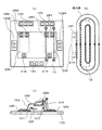
図1に本発明の電力変換装置の実施例1の斜視構成図を、図2にその上面図を、図3にその側面図を示す。本実施例は、ほぼ同じ形状の2つの半導体モジュール11、12を並列接続した実装構成であり、基本構成としては特許文献5に記載のものと同様である。
FIG. 1 is a perspective configuration diagram of a power converter according to a first embodiment of the present invention, FIG. 2 is a top view thereof, and FIG. 3 is a side view thereof. The present embodiment is a mounting configuration in which two
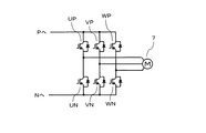
本実施例は、図4に示す一般的な3相インバータ回路に適用可能なものである。ここでは、半導体スイッチング素子の一例として、絶縁ゲート型バイポーラトランジスタIGBTを適用したものして説明する。図4において、図示していない直流電源あるいは平滑コンデンサから、3相インバータ回路を介して負荷7を駆動する構成となっている。1相を構成する直列接続された正極側及び負極側の一対の半導体スイッチング素子(図中で例えば、UP、UN)が交互にオン・オフを繰り返すことで、任意の周波数及び電圧の交流電力を負荷7に供給する。必要な電力が大きい場合には、1相分を複数の半導体スイッチング素子を並列した構成とすることがある。
This embodiment can be applied to the general three-phase inverter circuit shown in FIG. Here, an example in which an insulated gate bipolar transistor IGBT is applied will be described as an example of the semiconductor switching element. In FIG. 4, a
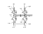
図5に、スイッチング素子を2個並列接続した1相分の回路構成を示す。ここでは、一対の半導体スイッチング素子111、112で1つの半導体モジュール11を、同様にスイッチング素子121、122とで1つの半導体モジュール12を構成している。すなわち、半導体モジュール11,12は、それぞれ、いわゆる2in1モジュールと称されている。
FIG. 5 shows a circuit configuration for one phase in which two switching elements are connected in parallel. Here, one
半導体モジュール11には、主電流が流れる正極端子11P、負極端子11N、交流端子110と、正極側の半導体スイッチング素子111をオン・オフする制御信号を入力するための制御端子11GP、負極側の半導体スイッチング素子112用の制御端子11GNがある。同様に、半導体モジュール12には主電流が流れる正極端子12P、負極端子12N、交流端子120と、正極側の半導体スイッチング素子121用の制御端子12GP、負極側の半導体スイッチング素子122用の制御端子12GNがある。例えば、半導体スイッチング素子111の制御は、制御端子11GPのゲート端子11GP1と制御用エミッタ端子11GP2との間にゲート信号を印加することで行われる。
The
本実施例の半導体モジュール11、12は、同一の形状及び構造を有し、扁平な直方体状に形成されている。各半導体モジュール11、12の長辺の縁部上面にそれぞれ主電流の正極端子11P、12P及び負極端子11N、12Nが設けられ、これに対向する長辺の縁部上面に交流端子110が設けられている。また、各半導体モジュール11、12の対向する2つの短辺の縁部上面に制御端子11GPと12GP、及び11GNと12GNがそれぞれ設けられている。
The
2個の半導体モジュール11、12の正極端子11P、12P及び負極端子11N、12Nは、図23に示す端子42,43,411,412を有する正極導体及び負極導体により並列接続されている。正極導体は、正極端子11Pに接続される折り曲げ端子を有し、半導体モジュール11、12の対向する長辺の縁部に沿って延在される導体バーと、正極端子12Pに接続される折り曲げ端子を有し、半導体モジュール12の長辺の縁部に沿って延在される導体バーの2つが設けられる。一方、負極導体は、負極端子11N、12Nにそれぞれ接続される折り曲げ端子を有し、半導体モジュール11、12の対向する長辺の縁部に沿って延在される導体バーを有して形成されている。これらの導体バーは、間隔を空けて積層状に配置され、3相インバータの他相の並列半導体モジュールとの接続に用いられる。
The
これらの接続導体は、特許文献6に記載のものと類似の形状に形成されている。つまり、負極端子11N、12Nに接続される負極導体が端子411、412を介して、図示していない直流電源あるいは平滑コンデンサの負極(図5のN)へ接続される。半導体モジュール11の正極端子11Pに接続される正極導体は、端子43を介して直流電源あるいは平滑コンデンサの正極(図5のP)へ接続される。半導体モジュール12の正極端子12Pに接続される正極導体は、端子42を介して直流電源あるいは平滑コンデンサの正極(図5のP)へ接続される。
These connection conductors are formed in a shape similar to that described in Patent Document 6. That is, the negative conductor connected to the
半導体モジュール内のスイッチング素子の駆動は、図示していないゲート駆動回路からゲート抵抗回路基板2に実装されているゲート抵抗、ゲート回路出力端子及びゲート配線を介して行われる。すなわち、ゲート駆動回路から共通ゲート配線31P、31N、ゲート抵抗回路入力端子21P、21Nを介してゲート抵抗回路基板2に駆動信号が入力される。
The switching element in the semiconductor module is driven from a gate drive circuit (not shown) through a gate resistor, a gate circuit output terminal, and a gate wiring mounted on the gate
図6に示すように、ゲート抵抗回路基板2の正極側入力端子21Pから個々のゲート抵抗243、244を介して正極側出力端子22P1、22P2、さらにゲート配線32P1、32P2を介して半導体モジュール11、12の正極側ゲート端子11GP、12GPにゲート駆動信号が印加される。
As shown in FIG. 6, from the
負極側についても同様で、ゲート抵抗回路基板2の負極側入力端子21Nから個々のゲート抵抗241、242を介して負極側出力端子22N1、22N2、さらにゲート配線32N1、32N2を介して、半導体モジュール11、12の負極側ゲート端子11GN、12GNにゲート駆動信号が印加される。
The same applies to the negative electrode side. From the negative electrode
図1ではゲート端子(例えば11GP)は簡略化したが、実際には図5に示すように、ゲート端子(例えば11GP1)と制御用エミッタ端子(例えば11GP2)とが1組になっている。同様に、ゲート配線(例えば32P1)も2本必要であり、この2本がツイストされた状態で用いられることが多い。図2では図の簡素化のためツイストされている部分を1本の太い線で表示している。ノイズによる誤動作抑制のためにシールド付きのツイスト線を用いられることもあり、その場合には丁度図2のような外観になる。 In FIG. 1, the gate terminal (for example, 11GP) is simplified, but actually, as shown in FIG. 5, the gate terminal (for example, 11GP1) and the control emitter terminal (for example, 11GP2) form one set. Similarly, two gate wirings (for example, 32P1) are required and are often used in a twisted state. In FIG. 2, the twisted portion is displayed with a single thick line for the sake of simplicity. A twisted wire with a shield may be used to suppress malfunction due to noise, and in that case, the appearance is exactly as shown in FIG.
図2において、ゲート抵抗回路基板2が被さっている半導体モジュール12の正極側ゲート端子12GPが図において左側に、負極側ゲート端子12GNが図において右側にある。一方、ゲート抵抗回路基板2が被さっていない半導体モジュール11の正極側ゲート端子11GPが図において右側に、負極側ゲート端子11GNが図において左側にある。
In FIG. 2, the positive side gate terminal 12GP of the
そこで、正極側スイッチング素子のゲート端子11GP、12GPに接続されるゲート配線32P1、32P2とゲート抵抗回路基板2とが接続されるゲート回路出力端子22P1、22P2がゲート抵抗回路基板2における右側に、負極側スイッチング素子のゲート端子11GN、12GNに接続されるゲート配線32N1、32N2とゲート抵抗回路基板2とが接続されるゲート回路出力端子22N1、22N2 がゲート抵抗回路基板2における左側に配置されている。このように配置することによって、ゲート抵抗回路基板2から遠い側のゲート端子11GP、11GNまでのゲート配線32P1、32N1と、ゲート抵抗回路基板2が被さっていてすぐ近くのゲート端子12GP、12GNまでのゲート配線32P2、32N2とを均等な長さにすることが容易である。
Therefore, the gate circuit output terminals 22P1 and 22P2 to which the gate wirings 32P1 and 32P2 connected to the gate terminals 11GP and 12GP of the positive side switching element and the gate
仮に、正極側のゲート回路出力端子22P1、22P2が左側、負極側のゲート回路出力端子22N1、22N2が右側にある場合には、ゲート回路出力端子からゲート端子までの距離が極端に異なるため均等な長さにすることが難しい。均等な長さにするには近い側の配線は長さに余りが生じるため、その部分でノイズを受けることが懸念されるからである。 If the positive side gate circuit output terminals 22P1 and 22P2 are on the left side and the negative side gate circuit output terminals 22N1 and 22N2 are on the right side, the distance from the gate circuit output terminal to the gate terminal is extremely different. It is difficult to make it long. This is because the wiring on the side closer to the uniform length has a surplus in length, and there is a concern that noise will be received at that portion.
図3は、2個の半導体モジュール11、12を右側面から見たときの図である。半導体モジュール11、12は放熱器6などに取り付けられる。図3の二点鎖線で囲んだ部分はスナバ回路51及び52であり、図1、図2では、半導体モジュールの各端子を見やすくするために、記載が省略されている。なお、スナバ回路51及び52は半導体スイッチング素子のスイッチング過渡時の跳ね上り電圧を抑制する役割を担うものであり、最も単純なものはコンデンサを接続したものである。その他にコンデンサとダイオードとの直列体及びコンデンサを放電するための抵抗とで構成したものがある。
FIG. 3 is a view of the two
図3の破線部20Pは、ゲート抵抗回路の部品部分であり、回路構成の例を図6に示す。図6において、上部は図5の回路を図2の実装構造に近い配置で記したものである。下部がゲート抵抗回路基板2の構成例を示している。図の最下部にあるゲート駆動回路基板29から、正極側の制御信号がゲート配線31Pを介してゲート抵抗回路基板2の入力端子21P1、21P2に、負極側の制御信号がゲート配線31Nを介してゲート抵抗回路基板2の入力端子21N1、21N2に伝えられる。入力端子21P1からは個々のゲート抵抗243、244を介して出力端子22P11及び22P21に分岐される。入力端子21P2からは出力端子22P12及び22P22に分岐される。
A
ここで、ゲート回路が外部ノイズの影響を受けないようにするため、後述する実施例のように、入力端子21P1〜出力端子22P11、出力端子22P12〜入力端子21P2で構成されるループ回路、及び入力端子21P1〜出力端子22P21、出力端子22P22〜入力端子21P2で構成されるループ回路のループ面積はできるだけ低減した構造になっている。出力端子22P11と22P12との間には、比較的高抵抗値の抵抗263とゲート過電圧抑制のためのツェナーダイオード2531、2532が接続されている。なお、負極側20N1、20N2についても回路構成は同じであるため、説明は省略する。
Here, in order to prevent the gate circuit from being affected by external noise, a loop circuit including an input terminal 21P1 to an output terminal 22P11, an output terminal 22P12 to an input terminal 21P2, and an input, as in an embodiment described later. The loop area constituted by the terminal 21P1 to the output terminal 22P21 and the output terminal 22P22 to the input terminal 21P2 has a structure in which the loop area is reduced as much as possible. Between the output terminals 22P11 and 22P12, a
以上説明したように、本実施例によれば、制御回路基板であるゲート抵抗回路基板2を2個の半導体モジュール11,12に対して1つにまとめて一方の半導体モジュール12の投影領域内に配置したことから、他方の半導体モジュール11の投影領域に電力変換装置の他の構成部品を配置することができるので、電力変換装置の小型化の実装構造に係る設計の自由度を増すことができる。
As described above, according to the present embodiment, the gate
また、並列接続された2個の半導体スイッチング素子111と121、112と122の制御端子11GPと12GP、11GNと12GNに供給するゲート信号を一つのゲート駆動回路29により生成していることから、並列素子の制御タイミングの差異をなくすことができる。
In addition, since the gate signals supplied to the control terminals 11GP and 12GP and 11GN and 12GN of the two
また、ゲート回路は、半導体モジュール11,12の正極側のスイッチング素子111,121を制御する正極側のゲート回路20P1と20P2、及び半導体モジュール11,12の負極側のスイッチング素子112,122を制御する負極側のゲート回路20N1,20N2とに分けて、ゲート抵抗回路基板2に搭載し、さらに正極側のゲート回路20P1と20P2は、ゲート抵抗回路基板2が重ねて配置された半導体モジュール2の負極側の制御端子12GN側に、負極側のゲート回路20N1,20N2は、ゲート抵抗回路基板2が重ねて配置された半導体モジュールの正極側の制御端子12GP側に配置された構成としているから、半導体モジュール11,12の正極側のゲート配線長及び負極側のゲート配線長をほぼ均等化することができる。特に、半導体スイッチング素子の各ゲートに供給するゲート抵抗回路の正極側出力端子22P1と22P2及び負極側出力端子22N1と22N2を、半導体モジュール11側に位置させて配置しているから、ゲート配線長を一層短くすることができる。
The gate circuit controls the positive-side gate circuits 20P1 and 20P2 that control the positive-
また、正極側出力端子22P1と22P2及び負極側出力端子22N1と22N2は、半導体モジュール11の正極側出力端子22P1及び負極側出力端子22N1をゲート抵抗回路基板2の外側に、ゲート抵抗回路基板2が配置された半導体モジュール12の正極側出力端子22P2及び負極側出力端子22N2を内側に配置することにより、ゲート配線長を一層均等化することができる。
The positive output terminals 22P1 and 22P2 and the negative output terminals 22N1 and 22N2 are arranged so that the positive output terminal 22P1 and the negative output terminal 22N1 of the
本発明の実施例2を図7、図8を用いて説明する。図7は、本実施例の斜視構成図であり、図8は本実施例の右側面図である。 A second embodiment of the present invention will be described with reference to FIGS. FIG. 7 is a perspective configuration diagram of the present embodiment, and FIG. 8 is a right side view of the present embodiment.
本実施例が実施例1と相違する点は、平滑コンデンサ50を正極導体の端子42、43及び負極導体の端子411、412に直接接続し、これに伴いスナバ回路51、52を除去したことにある。つまり、半導体モジュールと平滑コンデンサとを近づけることにより、配線の浮遊インダクタンスが低減できるので、スイッチング時の跳ね上り電圧を抑制できるためのスナバ回路を除去することが可能となる。
This embodiment differs from the first embodiment in that the smoothing
そして、本実施例では、スナバ回路52が無くなったので、ゲート抵抗回路基板2を半導体モジュール12の上表面に近づけて配置している。これによりゲート抵抗回路基板2から半導体モジュールのゲート端子(例えば12GN)までの距離が小さくなりゲート配線(例えば32N2)を短くできるため、一層ノイズの影響を受けにくくなるとともに、使用する配線が少なくて済むという利点がある。
In this embodiment, since the
さらに、それにより空いたスペースにゲート駆動回路29を配置することで更なる小型化を図っている。
In addition, the
ところが、ゲート抵抗回路基板2が半導体モジュールに近づけたことで半導体モジュール内部を流れる電流の影響を受けやすくなる。半導体モジュール内部電流とその電流による磁界の概略を図9、図10に示す。図9は正極側スイッチング素子導通時で、図10は負極側スイッチング素子導通時であり、それぞれ同図(a)はモジュール上面から、同図(b)は側面から、同図(c)は前面から見た図である。これらの磁界の概要は、特許文献5に記載されている。
However, since the gate
図9(c)のように正極側の半導体スイッチング素子導通時は、モジュール内部正極導体120Pからボンディングワイヤ1211、半導体素子部122P、ボンディングワイヤ1212を介して出力導体1200に電流が流れる。この電流が作る磁界はボンディングワイヤ1211と1212とで囲まれた領域では、紙面の手前から奥に、ボンディングワイヤ1212の上部では紙面の奥から手前に向かう向きである。この磁力線の概略を同図(b)に実線で示した。ゲート抵抗回路基板2の部分には、図9(a)、(b)において上から下、すなわち出力端子22N1、22N2から入力端子20Nに向かう向きとなる。
As shown in FIG. 9C, when the semiconductor switching element on the positive electrode side is conductive, current flows from the module internal
一方、図10(c)のように負極側の半導体スイッチング素子導通時は、出力導体1200からボンディングワイヤ1213、半導体素子部122N、ボンディングワイヤ1214を介してモジュール内部負極導体120Nに電流が流れる。この電流が作る磁界はボンディングワイヤ1213と1214とで囲まれた領域では、紙面の奥から手前に、ボンディングワイヤ1214の上部では紙面の手前から奥に向かう向きである。この磁力線の概略を同図(b)に実線で示した。ゲート抵抗回路基板2の部分には図10(a)、(b)において下から上、すなわち入力端子21Pから出力端子22P1、22P2に向かう向きとなる。
On the other hand, when the semiconductor switching element on the negative electrode side is conductive as shown in FIG. 10C, a current flows from the
これらの磁界は、スイッチング時の電流変化により変動するから、電磁誘導ノイズ等のノイズ要因になることが懸念される。そこで、ゲート抵抗回路基板2の構造を図11〜図13に示すようにする。図11(a)は、ゲート抵抗回路基板2の表面から、同図(b)は表側より裏面配線パターンを透視した図を示している。また、図12(a)は表面、同図(b)は裏面の配線パターンを示している。図12(b)は裏面から見た図である。図11、図12において、正極側のゲート抵抗回路基板200Pと負極側のゲート抵抗回路基板200Nとでは、部品配置及び配線パターンを同じにしている。そのため、ゲート抵抗回路基板2を図11、図12において左右に二分割すると、同一の回路基板となる。したがって、場合によっては二分割した同一回路基板を2つ並べても良い。
Since these magnetic fields fluctuate due to current changes during switching, there is a concern that they may cause noise such as electromagnetic induction noise. Therefore, the structure of the gate
図13は、図11における矢視A−A’図である。図中の点線は半導体モジュール内部の正極側の半導体スイッチング素子導通時の電流による磁力線を示している。ゲート抵抗回路基板2の表側パターンと裏側パターンとの間を通る磁界は、図において上下方向である。それに対して、抵抗241及び261を磁界の向きに実装しているため、抵抗、抵抗リード部分及び配線パターンとで構成されるループ回路を貫く磁界を低減できており、磁界の影響を受けにくい実装となっている。すなわち、抵抗、抵抗リード部分及び配線パターンとで構成されるループ回路全体の延在方向を、半導体スイッチング素子導通時の電流による磁力線の向きに平行に構成したことから、電磁誘導ノイズに係る磁束の鎖交数を低減することができる。
FIG. 13 is an arrow A-A ′ view in FIG. 11. The dotted line in the figure shows the lines of magnetic force due to the current when the semiconductor switching element on the positive electrode side inside the semiconductor module is conducted. The magnetic field passing between the front side pattern and the back side pattern of the gate
上述したように、本実施例によれば、ゲート抵抗回路基板2を、半導体モジュール12の投影領域内に、その半導体モジュール12の内部電流による電磁誘導ノイズを受けるような近接位置に配置しても、抵抗241及び261を磁界の向きに実装しているため、抵抗、抵抗リード部分及び配線パターンとで構成されるループ回路を貫く磁界を低減でき、磁界の影響を受けにくい実装とすることができる。つまり、電磁誘導ノイズに係る磁束が貫通するループ回路を低減した、言い換えれば、ループ回路に鎖交する電磁誘導ノイズに係る磁束の鎖交数を低減した回路構成にする。
As described above, according to the present embodiment, the gate
本実施例によれば、ゲート抵抗回路基板2を半導体モジュール12に接近して配置しても、内部電流による電磁誘導ノイズの影響を低減できる。したがって、ゲート抵抗回路基板2を半導体モジュール12の投影領域内であっても、半導体モジュール12から離して配置する必要がないので、設計の自由度を一層向上できる。
According to this embodiment, even if the gate
なお,図8に示したようにゲート駆動回路29は半導体モジュール12表面から離れているため、半導体モジュール12の内部電流が作る磁界の影響は受けにくく、ここに配置しても問題はない。
As shown in FIG. 8, since the
したがって、本実施例のように、2つの半導体モジュールを並列に接続し、一方の半導体モジュールの投影領域内に平滑コンデンサを配置することにより、スナバ回路を省略できるから、ゲート抵抗回路基板2を他方の半導体モジュールに近接して配置することができるので、電力変換装置の小型化をさらに図ることができる。 Therefore, as in this embodiment, the snubber circuit can be omitted by connecting two semiconductor modules in parallel and arranging a smoothing capacitor in the projection region of one of the semiconductor modules. Therefore, the power conversion device can be further downsized.
本発明の実施例3を図14〜図18を用いて説明する。図14は、ゲート抵抗回路基板2の回路構成を示す。本実施例は、図6のゲート抵抗回路基板2から、ツェナーダイオード(例えば、2511、2512)を除いた点が相違することから、他の構成の説明は省略する。本実施例のツェナーダイオードは、各半導体スイッチに対応させて分岐して設けたゲート抵抗回路の分岐前のゲート駆動回路基板29側に設けられている。この点は、特許文献2の場合と同様である。
A third embodiment of the present invention will be described with reference to FIGS. FIG. 14 shows a circuit configuration of the gate
図15及び図16に、ゲート抵抗回路基板2の実装構成及び配線パターンを示す。ここでは、抵抗241〜244及び261〜264を図において横方向に延在させて実装している。また、中心線C−C’に関して対称の構成にしている。このゲート抵抗回路基板2を図7と同じように設置すると半導体モジュール12内部電流による磁界は図9及び図10と同じようになる。
15 and 16 show a mounting configuration and a wiring pattern of the gate
本実施例の場合、抵抗261が受ける磁界の様子を図17に、抵抗263が受ける磁界の様子を図18に示す。正極側の半導体スイッチング素子が導通することにより半導体モジュール内部電流による磁界は図9に示したような向きとなるため、図17の矢印で示す向きの磁界が増大することになる。図17において、抵抗261のリードは片方が表面パターン271と接続点(スルーホール等)2712で接続され配線パターン271を介して接続点2711に接続される。他方は裏面パターン281と接続点2812で接続され配線パターン281を介して接続点2811に接続される。このとき半導体モジュール内部電流による磁界変化により、抵抗261とそのリード及び配線パターンで構成されるループを1ターンコイルとみなせて、図示したように端子2711がマイナス、端子2811がプラスとなる向きに誘起電圧が発生する。端子2711は、出力端子22N1を介して負極側の半導体スイッチング素子のゲート端子11GN1に接続され、端子2811は、出力端子22N1を介して負極側スイッチング素子の制御用エミッタ端子11GN2に接続される。このため、負極側の半導体スイッチング素子(図5の112)をオフさせる向き、すなわち誤動作を抑制する方向に作用する。図示していないが、もう一方の負極側の半導体スイッチング素子についても同様である。
In the case of this embodiment, the state of the magnetic field received by the
また、正極側の半導体スイッチング素子がターンオフする時には、図17の矢印で示す向きの磁界が減少することになり、図示した符号と逆の極性に誘起電圧が発生するが、正極側の半導体スイッチング素子のターンオフに影響を及ぼすわけではないので問題ない。 In addition, when the semiconductor switching element on the positive electrode side is turned off, the magnetic field in the direction indicated by the arrow in FIG. 17 is reduced, and an induced voltage is generated with a polarity opposite to the sign shown in the figure. There is no problem because it does not affect the turn-off.
一方、負極側の半導体スイッチング素子が導通することにより半導体モジュール内部電流による磁界は図10に示したような向きとなるため、図18の矢印で示す向きの磁界が増大することになる。その磁界変化により、抵抗263とそのリード及び配線パターンで構成されるループを1ターンコイルとみなせて、図示したように端子2821がプラス、端子2731がマイナスとなる向きに誘起電圧が発生する。端子2731は出力端子22P1を介して、正極側の半導体スイッチング素子のゲート端子11GP1に接続され、端子2821は出力端子22P1を介して、正極側の半導体スイッチング素子の制御用エミッタ端子11GP2に接続されるため、正極側の半導体スイッチング素子(図5の111)をオフさせる向き、すなわち誤動作を抑制する方向に作用する。図示していないが、もう一方の正極側の半導体スイッチング素子についても同様である。
On the other hand, when the semiconductor switching element on the negative electrode side is turned on, the magnetic field due to the internal current of the semiconductor module is oriented as shown in FIG. 10, and the magnetic field in the direction shown by the arrow in FIG. 18 increases. Due to the change in the magnetic field, a loop composed of the
また、負極側の半導体スイッチング素子がターンオフする時には、図18の矢印で示す向きの磁界が減少することになり、図示した符号と逆の極性に誘起電圧が発生するが、負極側スイッチング素子のターンオフに影響を及ぼすわけではないので問題ない。 Further, when the semiconductor switching element on the negative electrode side is turned off, the magnetic field in the direction indicated by the arrow in FIG. 18 is reduced, and an induced voltage is generated in the opposite polarity to the illustrated sign. There is no problem because it does not affect.
以上説明したように、本実施例3によれば、ゲート抵抗回路基板2の抵抗とリード線と配線パターンからなるループ回路の延在方向を、半導体モジュール内部電流により生ずる磁界の向きに直交する方向に合わせているが、電磁誘導ノイズに係る磁束の変化により抵抗回路に誘起される電流の向きが、ゲート抵抗回路を誤動作させない向きになるから、ゲート抵抗回路基板2を半導体モジュールに接近して配置しても、内部電流による電磁誘導ノイズの影響を低減できる。
As described above, according to the third embodiment, the extending direction of the loop circuit composed of the resistance of the gate
本発明の実施例4について、図19〜図24を用いて説明する。本実施例は、図19に示すように、図4に示す三相インバータの各スイッチング素子部分を2並列接続構成とした場合の実装例を示している。 A fourth embodiment of the present invention will be described with reference to FIGS. As shown in FIG. 19, the present embodiment shows a mounting example in which each switching element portion of the three-phase inverter shown in FIG. 4 has a two-parallel connection configuration.
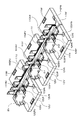
半導体モジュール11U、12Uが並列でU相、11V、12Vが並列でV相、11W、12Wが並列でW相を構成している。図において手前側の半導体モジュール12U、12V、12Wの正極端子12UP、12VP、12WPを接続している正極導体、各半導体モジュール11U〜12Wの負極端子(図で見えているのは12UN、12VN、12WN)を接続している負極導体、反対側の半導体モジュール11U、11V、11Wの正極端子(図では隠れているため図示せず)を接続している奥側正極導体が横に長く跨っている。
The
このうちV相の部分を拡大して図20に示す。図1の実施例1の実装とほぼ同じであるが、前述のように負極導体及び2つの正極導体が横に長く跨っているため、ゲート抵抗回路基板2から奥側の制御端子11GPV及び11GNVへのゲート配線が手前側の半導体モジュール12Vの正極端子12PVと負極端子12NVとにより形成される空間部を通している。ゲート配線をこの空間部を通した理由を図21〜図24で説明する。
Of these, the V-phase portion is enlarged and shown in FIG. Although it is almost the same as the mounting of the first embodiment of FIG. 1, since the negative electrode conductor and the two positive electrode conductors are horizontally long as described above, from the gate
まず、図21は、2並列接続された1相分の動作電流を示している。始め上側スイッチング素子111及び121はオフした状態で、図中、二点鎖線で通流経路を示すように、下側112及び122の環流ダイオードに電流が流れた状態から、上側スイッチング素子111及び121がターンオンして図中の実線の通流経路に変わる状態について説明する。
First, FIG. 21 shows an operating current for one phase connected in parallel. At the beginning, the
始めは負極導体の端子411及び412から負極端子11N及び12Nに電流が流れ込んでおり、正極側の半導体スイッチング素子がターンオンすることにより、実線の経路、すなわち、片方の正極導体の接続端子43から片方の正極端子11Pに、もう一方の正極導体の端子42から正極端子12Pに電流が流れるように変化する。
At first, current flows from the
この時の実装上の電流経路を図22及び図23に示す。図23は積層された3導体を分解して図示したものである。両図において、(1)負側環流時は図21における二点鎖線の経路であり、(2)正側導通時は図21における実線の経路である。 Current paths on mounting at this time are shown in FIGS. FIG. 23 is an exploded view of three stacked conductors. In both figures, (1) the negative side reflux is a two-dot chain line path in FIG. 21, and (2) the positive side conduction is a solid line path in FIG.
図24に、この時の電流による磁界の変化を示す。(1)負側環流時では負側導体の端子411及び412から図において下向きに電流が流れているため、図中の領域A及び領域Cでは紙面の奥から手前に向かう磁界が支配的で、領域Bでは反対に紙面の手前から奥に向かう磁界が支配的である。また、奥側の半導体モジュール11の負極端子11Nへ点線で示した下向きの電流が流れ、手前側の半導体モジュール12の負極端子12Nへも下向きの電流が流れている。並列接続した両方の電流がほぼ均等とすると領域Dでは紙面に垂直な方向の磁界は概ねゼロである。
FIG. 24 shows the change of the magnetic field due to the current at this time. (1) At the time of negative side circulation, since current flows downward from the
次に、(2)正側導通時は、正極導体の端子42及び43から電流が流れるため、領域A及び領域Cでは紙面の手前から奥に向かう磁界が支配的で、領域Bでは紙面の奥から手前に向かう磁界が支配的である。そのため、領域A、領域B、領域Cではスイッチング時には大きく磁界が変化する。もしこの部分にゲート配線が通ると磁界の影響を受ける可能性がある。ゲート配線はツイストするなど外部磁界変化の影響を受けにくくするのが一般的であるが、ツイストの粗さなどにより全く影響を受けないとは言い切れないこともあるため、このように磁界変化の大きい場所は配線経路としては避ける方が好ましい。
Next, (2) at the time of positive-side conduction, current flows from the
一方、領域Dに関しては、(2)正側導通時でもほとんど変化がないので、本実施例においては、この領域をゲート配線経路にした。なお、領域Dでなく、その両脇の領域E、領域Fでは磁界がゼロではないがスイッチングによって磁界の向きは大きく変わらないためこの部分をゲート配線経路としても良く、図7のゲート配線32P1は領域Fを、ゲート配線32N1は領域Eを通っていることになる。 On the other hand, since there is almost no change in the region D even when (2) it is on the positive side, this region is used as a gate wiring path in this embodiment. Note that the magnetic field is not zero in the regions E and F on both sides of the region D, but not in the region D, but the direction of the magnetic field does not change greatly by switching, so this portion may be used as a gate wiring path, and the gate wiring 32P1 in FIG. In the region F, the gate wiring 32N1 passes through the region E.
すなわち、本実施例によれば、3相インバータ回路を1相あたり2並列の半導体モジュールにより構成する場合において、一方の半導体モジュール12に重ねて配置されたゲート抵抗回路基板2から、他方の半導体モジュール11の制御端子11GP,11GNに接続するゲート配線を、2並列の半導体モジュール11,12の正極端子11Pと12P及び負極端子11Nと12Nにより形成される隙間(領域D)を通していることから、主回路に流れる電流による磁界の影響を受けることなく配線することができる。
In other words, according to the present embodiment, when the three-phase inverter circuit is configured by two parallel semiconductor modules per phase, the gate
すなわち、本実施例のように3相インバータを構成する場合、2並列接続した半導体モジュールを3つ又は2つ並べて電力変換装置を構成することになる。これらの場合、各半導体モジュールの正極端子と負極端子を共通に接続する板状の正極導体と負極導体が必要になる。この場合、図23等に示すように、共通の負極導体を挟んで2枚の共通の正極導体を間隔をあけて配置し、それらの共通導体を並べた複数の半導体モジュールに跨って配設することになる。この場合、直流電源に接続される端子42,43,411,412は、重ねて配設された共通の正極導体及び負極導体から突出させて形成される。
That is, when a three-phase inverter is configured as in this embodiment, the power conversion device is configured by arranging two or two semiconductor modules connected in parallel. In these cases, a plate-like positive electrode conductor and a negative electrode conductor that commonly connect the positive electrode terminal and the negative electrode terminal of each semiconductor module are required. In this case, as shown in FIG. 23 and the like, two common positive electrode conductors are arranged at intervals with a common negative electrode conductor interposed therebetween, and are arranged across a plurality of semiconductor modules in which the common conductors are arranged. It will be. In this case, the
したがって、正極導体及び負極導体は、半導体モジュール11,12の11P、12P、及び負極端子11N、12Nにそれぞれ接続された正極導体と負極導体とが近接対向して配設された第1の部分と、それらが近接対向して配設されていない第2の部分(領域A,B,Cを画成する導体部分)とが形成される。この場合、第1の部分の近傍の領域E,D,Fに制御回路基板2から半導体モジュール11の制御端子11GP、11GNに至るゲート配線32P1,32N1を通すことが好ましい。これにより、主回路に流れる電流による磁界の影響を受けることなくゲート配線をすることができる。
Therefore, the positive electrode conductor and the negative electrode conductor are the first part in which the positive electrode conductor and the negative electrode conductor respectively connected to 11P and 12P of the
本発明の実施例5について、図25〜図28を用いて説明する。 A fifth embodiment of the present invention will be described with reference to FIGS.
図25は、ゲート抵抗回路の並列接続されたゲート端子相互間をゲート感度補正抵抗240P及び240Nで接続した例であり、この点は、特許文献7に記載されている通り公知である。ここで、ゲート感度補正抵抗は、半導体モジュールのゲート端子相互間を接続するのが好ましいが、抵抗を実装する場所の問題から本実施例ではゲート抵抗回路基板2に実装することにした。
FIG. 25 is an example in which gate
この時のゲート抵抗回路基板2の実装を図26に、回路の配線パターンを図27に、図26における側面を図28に示す。全体実装としては図7に示したものと同じ場合を考える。
The mounting of the gate
ゲート感度補正抵抗240P及び240Nは図26、図28において図中の縦方向に実装しており、つまり図11の実施例2で説明したのと同様に抵抗のループ回路の向き(断面)を主回路電流による磁界の向きに平行に配置したことから、図28に磁力線を示す磁界の影響を受けにくい。そのため、並列接続したゲート端子間に影響を及ぼすことがない。なお、図26、図27において、ゲート感度補正抵抗240Pはゲート抵抗244の脇に置いたが、ゲート抵抗243の脇に置いて、それに応じた配線パターンにしてもよく、同様にゲート感度補正抵抗240Nをゲート抵抗241の脇でなくゲート抵抗242の脇においてそれに応じた配線パターンにしても構わない。
The gate
本実施例によれば、ゲート感度補正抵抗240P,240Nをゲート抵抗回路基板2に実装することができ、かつ、それらの抵抗のループ回路の向きを主回路電流による磁界の向きに平行に配置したことから、主回路電流による電磁ノイズの影響を受けることがない実装構造を実現できる。
According to the present embodiment, the gate
本発明の実施例6について、図29〜図31を用いて説明する。 A sixth embodiment of the present invention will be described with reference to FIGS.
図29は、交流電源8からPWM整流回路を介して電力を供給している場合の回路構成であり、力率改善や電力回生する場合に一般的に用いられている。なお図29では、交流電源8のみとしたが、電源の後段にフィルタあるいは昇圧リアクトルが接続される場合もある。ここでは、PWM整流回路の各相は各々1つの半導体モジュール1R、1S、1Tで構成されており並列接続はしていない。負荷7に接続されるインバータに関しても同様に並列接続していなく3つの半導体モジュール1U、1V、1Wで構成されている。各々の半導体モジュールにはゲート抵抗回路基板2R、2S、2T、2U、2V及び2Wから制御端子に接続されている。
FIG. 29 shows a circuit configuration when power is supplied from the
図30に本実施例の実装例を示す。各半導体モジュール(例えば1U)に被さるように各ゲート抵抗回路基板(例えば2U)が実装されており、その出力端子(例えば22PU)から制御端子(例えば1UGP)にゲート配線を介して接続されている。この時の特徴としては図1では被さっている半導体モジュール12ではない方の半導体モジュール11の負側制御端子11GNに接続されていた出力端子22N1を、図30の場合には被さっている半導体モジュール1Uの正側制御端子1UGPに接続される出力端子22PUとして使うことでゲート配線長さを短くできることである。
FIG. 30 shows a mounting example of this embodiment. Each gate resistor circuit board (for example, 2U) is mounted so as to cover each semiconductor module (for example, 1U), and is connected to the control terminal (for example, 1UGP) from its output terminal (for example, 22PU) through a gate wiring. . As a feature at this time, the output terminal 22N1 connected to the negative control terminal 11GN of the
同じ形状の半導体モジュールのためのゲート抵抗回路基板2を並列接続時と非並列とで2種類に分けて準備しておくのは保守管理の観点で言えば得策ではない。まして、並列接続が必要なものはかなりの大電力用であるため用途も限られてくる。そこで、1種類のゲート抵抗回路基板に統一することで保守管理部品の種類が少なくなり、故障時の対応が迅速になるためサービスの低下を最小限に抑制することが可能になると考えられる。
From the viewpoint of maintenance management, it is not a good idea to prepare the gate
図11及び図12で示したゲート抵抗回路基板は、正側回路基板200Pと負側回路基板200Nとは同じ構造であるため、正負を逆に使用しても構わない。このように正側回路と負側回路とを同一構造にしておくことで図29〜図30のように並列接続しない場合にも流用することが可能であり、保守管理部品の種類低減が可能となる。
Since the
また、図31は、図11、図12で示した同じ回路パターンに必要な部品のみを実装したものである。図11、図12では図の右側を正側回路基板200P、左側を負側回路基板200Nとすることでゲート配線長さの均等化を図れた。しかし、図31では左側に正側回路を、右側に負側回路とすることで図30に示すように半導体モジュールの制御端子との配線を短くすることが可能となっている。
FIG. 31 shows only the components necessary for the same circuit pattern shown in FIG. 11 and FIG. In FIG. 11 and FIG. 12, the right side of the figure is the
また、図31はゲート抵抗回路基板2Uとしては図12と同じ配線パターンを用いて、必要な部分の部品のみを実装している。使用する対象が並列接続した場合に流用しないことが確実であれば、不要な部品は除去しておくことができる。
In FIG. 31, only the necessary parts are mounted using the same wiring pattern as that of FIG. 12 as the gate
なお、図31では抵抗241及び261は図において縦方向に実装されているため、半導体モジュール内部電流による磁界の変化の影響は受けにくく問題とはならない。
In FIG. 31, since the
本発明の実施例7について、図32〜図33を用いて説明する。 A seventh embodiment of the present invention will be described with reference to FIGS.
図32の本実施例は、実施例1、4の主回路の接続導体の構成が異なる。本実施例では、半導体モジュール11と12とを並列接続する主回路配線の導体が、半導体モジュール11と12の正極端子11P,12P及び負極端子11N,12Nの端子面と平行に設けている。そのため、2つの半導体モジュール11,12の間隔が広くなり、ゲート抵抗回路基板2の出力端子22P1から制御端子11GPまでの距離、同様に出力端子22N1から制御端子11GNまでの距離が一層遠くなっている。このような実装構造は、特許文献8に記載された構造と類似である。
The present embodiment of FIG. 32 differs in the configuration of the connection conductors of the main circuit of the first and fourth embodiments. In this embodiment, the conductor of the main circuit wiring that connects the
図33に、本実施例のゲート抵抗回路基板2の実装構造を示す。本実施例では、図11に比べて負側入力端子21Nが図の左側に寄っており、出力端子22N1までの電流経路がもう一方の出力端子22N2までの電流経路に比べて短くなっている。同様に、正側入力端子21Pが図の右側に寄って、出力端子22P1までの電流経路がもう一方の出力端子22P2までの電流経路に比べて短くなっている。
FIG. 33 shows the mounting structure of the gate
すなわち、出力端子から制御端子までのゲート配線32P1と32P2とでは距離の差が大きいため、配線長さを揃えると近い側のゲート配線32P2がかなり余ってしまう。この余りの部分に磁界が鎖交すると誤動作などの要因になる可能性があるため好ましくない。そこで、本実施例では、ゲート抵抗回路基板2の内部の配線経路に差をつけて、ゲート配線長さの差を緩和することで並列接続間の不均等を低減している。
That is, since the difference in distance between the gate wirings 32P1 and 32P2 from the output terminal to the control terminal is large, the gate wiring 32P2 on the near side is considerably left when the wiring lengths are made uniform. If the magnetic field is linked to the remaining portion, it may cause a malfunction or the like, which is not preferable. Therefore, in this embodiment, the difference between the parallel wirings is reduced by making a difference in the wiring path inside the gate
本発明の実施例8を図34〜図35に示す。本実施例は、図1に示した2並列接続の構成をさらに横に2個並べて、全体で4並列接続の構成にした場合である。ゲート抵抗回路基板2Aから半導体モジュール11と12にゲート配線が接続され、もう一方のゲート抵抗回路基板2Bから半導体モジュール13と14にゲート配線が接続されている。
An eighth embodiment of the present invention is shown in FIGS. In this embodiment, the two parallel connection configurations shown in FIG. 1 are further arranged side by side to form a total of four parallel connection configurations. Gate wiring is connected to the
4並列接続の半導体モジュール11,12,13,14に対して、共通のゲート駆動回路から配線31Pから分岐点31P0を介してゲート配線31P1及び31P2に分岐され、ゲート抵抗回路基板2A及び2Bの正側入力端子2A1P及び2B1Pに接続する。同様に配線31Nから分岐点31N0を介してゲート配線31N1及び31N2に分岐され、ゲート抵抗回路基板2A及び2Bの負側入力端子2A1N及び2B1Nに接続する。分岐点31P0及び31N0は3組の配線をカシメ接続やハンダ接続により接続する。
For the four parallel-connected
2つのゲート抵抗回路基板2A及び2Bから各々2個の半導体モジュール11、12及び13、14へのゲート配線については図1の場合と同様なので説明は省略する。
The gate wiring from the two gate
このように2並列接続の構造を基本として複数組設けることで2、4、6並列と並列数を増加して変換器容量を増大することが可能である。並列数が増加した場合に、分岐点31P0の分岐する配線数が増大するため、図示していないゲート駆動回路の出力端子から直接複数組の配線を接続したり、ゲート駆動回路の出力端子を複数組設けるなどもできる。 Thus, by providing a plurality of sets based on the structure of two parallel connections, it is possible to increase the converter capacity by increasing the number of parallels to 2, 4, 6 parallel. When the number of parallel increases, the number of wiring branches at the branch point 31P0 increases. Therefore, a plurality of sets of wirings can be directly connected from the output terminal of the gate driving circuit (not shown), or a plurality of output terminals of the gate driving circuit can be connected. A set can also be provided.
以上、本発明を実施例1〜8に基づいて説明したように、本発明によれば、電力変換装置の小型化を図りつつ、並列接続時の電流分担不均等を抑制することが可能となる。 As described above, the present invention has been described based on the first to eighth embodiments. According to the present invention, it is possible to suppress current sharing unevenness during parallel connection while reducing the size of the power conversion device. .
なお、本発明はそれらの実施例に限定されるものではなく、例えば、半導体スイッチング素子として、IGBTに限らず、他の周知のスイッチング素子にも適用できるのは言うまでもない。 In addition, this invention is not limited to those Examples, For example, as a semiconductor switching element, it cannot be overemphasized that it is applicable not only to IGBT but another known switching element.
2 ゲート抵抗回路基板
6 放熱器
7 負荷
8 電源
11、12 半導体モジュール
31P、31N、32P1、32P2、32N1、32N2 ゲート配線
42、43、411、412 端子
50 平滑コンデンサ
51、52 スナバ回路
2 Gate resistance circuit board 6
Claims (9)
前記第1と第2の半導体モジュールの各スイッチング素子をそれぞれ制御する制御回路が搭載された制御回路基板を、一方の半導体モジュールの投影領域内に配置し、
前記制御回路は、前記第1と第2の半導体モジュールの正極側のスイッチング素子を制御する正極制御回路と、前記第1と第2の半導体モジュールの負極側のスイッチング素子を制御する負極制御回路とに分けて前記制御回路基板に搭載され、
前記正極制御回路は、前記制御回路基板が配置された半導体モジュールの前記負極制御端子側に、前記負極制御回路は、前記制御回路基板が配置された半導体モジュールの正極制御端子側に配置されていることを特徴とする電力変換装置。 The first and second semiconductor modules having the same configuration are connected in parallel to each other, and the semiconductor module is provided in a pair of positive and negative semiconductor switching elements connected in series and at the edge of each semiconductor module. A positive electrode terminal and a negative electrode terminal connected to the pair of semiconductor switching elements, and a positive electrode that is provided at an opposite edge different from the edge where the positive electrode terminal and the negative electrode terminal are located and controls the pair of semiconductor switching elements, respectively. In the power converter configured to have a control terminal and a negative electrode control terminal,
A control circuit board on which a control circuit for controlling each switching element of each of the first and second semiconductor modules is mounted is disposed in a projection region of one semiconductor module,
The control circuit includes: a positive control circuit that controls switching elements on the positive side of the first and second semiconductor modules; a negative control circuit that controls switching elements on the negative side of the first and second semiconductor modules; Is mounted on the control circuit board,
The positive electrode control circuit, the negative electrode control terminal of the semiconductor module, wherein the control circuit board is arranged, the negative electrode control circuit is arranged to the positive control terminal of the semiconductor module, wherein the control circuit board is arranged The power converter characterized by the above-mentioned.
前記第1と第2の半導体モジュールの各スイッチング素子をそれぞれ制御する制御回路が搭載された制御回路基板を、一方の半導体モジュールの投影領域内に配置し、
前記制御回路基板は、前記半導体モジュールの投影領域内に当該半導体モジュールの内部電流による電磁誘導ノイズの影響を受ける位置に配置され、
前記制御回路は、前記電磁誘導ノイズに係る磁束が鎖交するループ回路の面積が低減するように回路部品が磁界の向きに実装されていることを特徴とする電力変換装置。 The first and second semiconductor modules having the same configuration are connected in parallel to each other, and the semiconductor module is provided in a pair of positive and negative semiconductor switching elements connected in series and at the edge of each semiconductor module. A positive electrode terminal and a negative electrode terminal connected to the pair of semiconductor switching elements, and a positive electrode that is provided at an opposite edge different from the edge where the positive electrode terminal and the negative electrode terminal are located and controls the pair of semiconductor switching elements, respectively. In the power converter configured to have a control terminal and a negative electrode control terminal,
A control circuit board on which a control circuit for controlling each switching element of the first and second semiconductor modules is mounted is disposed in the projection region of one semiconductor module,
The control circuit board is disposed at a position affected by electromagnetic induction noise due to an internal current of the semiconductor module in the projection area of the semiconductor module,
Wherein the control circuit, power conversion device, wherein a circuit component is mounted in the direction of the magnetic field such that the area of the loop circuit flux according to the electromagnetic induction noise interlinked is reduced.
前記第1と第2の半導体モジュールの各スイッチング素子をそれぞれ制御する制御回路が搭載された制御回路基板を、一方の半導体モジュールの投影領域内に配置し、
前記制御回路基板は、前記半導体モジュールの投影領域内に当該半導体モジュールの内部電流による電磁誘導ノイズの影響を受ける位置に配置され、
前記制御回路は、前記電磁誘導ノイズに係る磁束が鎖交するループ回路の向きを、前記磁束の変化により当該制御回路が誤動作しない向きに配置されたことを特徴とする電力変換装置。 The first and second semiconductor modules having the same configuration are connected in parallel to each other, and the semiconductor module is provided in a pair of positive and negative semiconductor switching elements connected in series and at the edge of each semiconductor module. A positive electrode terminal and a negative electrode terminal connected to the pair of semiconductor switching elements, and a positive electrode that is provided at an opposite edge different from the edge where the positive electrode terminal and the negative electrode terminal are located and controls the pair of semiconductor switching elements, respectively. In the power converter configured to have a control terminal and a negative electrode control terminal,
A control circuit board on which a control circuit for controlling each switching element of each of the first and second semiconductor modules is mounted is disposed in a projection region of one semiconductor module,
The control circuit board is disposed at a position affected by electromagnetic induction noise due to an internal current of the semiconductor module in the projection area of the semiconductor module;
The power converter according to claim 1, wherein the control circuit is arranged such that a direction of a loop circuit in which a magnetic flux related to the electromagnetic induction noise is linked is a direction in which the control circuit does not malfunction due to a change in the magnetic flux.
前記半導体モジュールの各スイッチング素子をそれぞれ制御する制御回路が搭載された制御回路基板を、前記半導体モジュールの投影領域内に配置し、
前記制御回路基板は、前記半導体モジュールの投影領域内に当該半導体モジュールの内部電流による電磁誘導ノイズの影響を受ける位置に配置され、
前記制御回路は、前記電磁誘導ノイズに係る磁束が鎖交するループ回路の面積が低減するように回路部品が磁界の向きに実装されていることを特徴とする電力変換装置。 A pair of positive and negative semiconductor switching elements connected in series, a positive terminal and a negative terminal connected to the pair of semiconductor switching elements, and edges having the positive terminal and the negative terminal are different from each other . In a power conversion device including a semiconductor module having a positive electrode control terminal and a negative electrode control terminal that are provided at an edge and respectively control the pair of semiconductor switching elements.
A control circuit board on which a control circuit for controlling each switching element of the semiconductor module is mounted is disposed in the projection area of the semiconductor module ,
The control circuit board is disposed at a position affected by electromagnetic induction noise due to an internal current of the semiconductor module in the projection area of the semiconductor module,
The power converter according to claim 1, wherein the control circuit has circuit components mounted in a magnetic field direction so as to reduce an area of a loop circuit in which magnetic flux related to the electromagnetic induction noise is linked .
前記半導体モジュールの各スイッチング素子をそれぞれ制御する制御回路が搭載された制御回路基板を、前記半導体モジュールの投影領域内に配置し、
前記制御回路基板は、前記半導体モジュールの投影領域内に当該半導体モジュールの内部電流による電磁誘導ノイズの影響を受ける位置に配置され、
前記制御回路は、前記電磁誘導ノイズに係る磁束が鎖交するループ回路の向きを、前記磁束の変化により当該制御回路が誤動作しない向きに配置されたことを特徴とする電力変換装置。 A pair of positive and negative semiconductor switching elements connected in series, a positive terminal and a negative terminal connected to the pair of semiconductor switching elements, and edges having the positive terminal and the negative terminal are different from each other. In a power conversion device including a semiconductor module having a positive electrode control terminal and a negative electrode control terminal that are provided at an edge and respectively control the pair of semiconductor switching elements.
A control circuit board on which a control circuit for controlling each switching element of the semiconductor module is mounted is disposed in the projection area of the semiconductor module,
The control circuit board is disposed at a position affected by electromagnetic induction noise due to an internal current of the semiconductor module in the projection area of the semiconductor module,
The power converter according to claim 1, wherein the control circuit is arranged such that a direction of a loop circuit in which a magnetic flux related to the electromagnetic induction noise is linked is a direction in which the control circuit does not malfunction due to a change in the magnetic flux.
前記制御回路は、前記電磁誘導ノイズに係る磁束が鎖交するループ回路の向きが、前記磁束の変化により当該制御回路が誤動作しない向きに配置されたことを特徴とする電力変換装置。 The power conversion device according to claim 2 ,
Wherein the control circuit, the orientation of the loop circuit flux interlinked according to electromagnetic induction noise, power conversion apparatus characterized by the control circuit is arranged in a direction that does not malfunction by a change in the magnetic flux.
前記第1と第2の半導体モジュールの各スイッチング素子をそれぞれ制御する制御回路が搭載された制御回路基板を、一方の半導体モジュールの投影領域内に配置し、
前記第1と第2の半導体モジュールの正極端子と負極端子にそれぞれ接続された正極導体と負極導体とが近接対向して配設された第1の部分と、前記正極導体と前記負極導体が近接して配設されていない第2の部分とが形成され、前記第1の部分の近傍の領域に前記制御回路基板から前記他の半導体モジュールの制御端子に至る配線を通すことを特徴とした電力変換装置。 The first and second semiconductor modules having the same configuration are connected in parallel to each other, and the semiconductor module is provided in a pair of positive and negative semiconductor switching elements connected in series and at the edge of each semiconductor module. A positive electrode terminal and a negative electrode terminal connected to the pair of semiconductor switching elements, and a positive electrode that is provided at an opposite edge different from the edge where the positive electrode terminal and the negative electrode terminal are located and controls the pair of semiconductor switching elements, respectively. In the power converter configured to have a control terminal and a negative electrode control terminal,
A control circuit board on which a control circuit for controlling each switching element of the first and second semiconductor modules is mounted is disposed in the projection region of one semiconductor module,
A first portion in which a positive electrode conductor and a negative electrode conductor connected to a positive electrode terminal and a negative electrode terminal of the first and second semiconductor modules, respectively, are disposed in close proximity to each other; and the positive electrode conductor and the negative electrode conductor are adjacent to each other And a second portion that is not arranged, and a wiring from the control circuit board to a control terminal of the other semiconductor module is passed through a region in the vicinity of the first portion. Conversion device.
前記第1と第2の半導体モジュールの各スイッチング素子をそれぞれ制御する制御回路が搭載された制御回路基板を、一方の半導体モジュールの投影領域内に配置し、
前記制御回路は、前記第1と第2の半導体モジュールの正極側のスイッチング素子を制御する2つの正極制御回路と、前記第1と第2の半導体モジュールの負極側のスイッチング素子を制御する2つの負極制御回路とが前記制御回路基板に搭載されてなり、
前記2つの正極制御回路と前記2つの負極制御回路の配線パターンが同一であることを特徴とする電力変換装置。 The first and second semiconductor modules having the same configuration are connected in parallel to each other, and the semiconductor module is provided in a pair of positive and negative semiconductor switching elements connected in series and at the edge of each semiconductor module. A positive electrode terminal and a negative electrode terminal connected to the pair of semiconductor switching elements, and a positive electrode that is provided at an opposite edge different from the edge where the positive electrode terminal and the negative electrode terminal are located and controls the pair of semiconductor switching elements, respectively. In the power converter configured to have a control terminal and a negative electrode control terminal,
A control circuit board on which a control circuit for controlling each switching element of the first and second semiconductor modules is mounted is disposed in the projection region of one semiconductor module,
The control circuit includes two positive control circuits that control the switching elements on the positive side of the first and second semiconductor modules, and two that control the switching elements on the negative side of the first and second semiconductor modules. A negative electrode control circuit is mounted on the control circuit board,
The power converter according to claim 1, wherein the two positive electrode control circuits and the two negative electrode control circuits have the same wiring pattern.
前記第1と第2の半導体モジュールの各スイッチング素子をそれぞれ制御する制御回路が搭載された制御回路基板を、一方の半導体モジュールの投影領域内に配置し、
前記制御回路は、前記第1と第2の半導体モジュールの正極側のスイッチング素子を制御する2つの正極制御回路と、前記第1と第2の半導体モジュールの負極側のスイッチング素子を制御する2つの負極制御回路とが前記制御回路基板に搭載されてなり、
前記2つの正極制御回路と前記2つの負極制御回路は、それぞれ対応する半導体スイッチング素子の制御端子の相互間を接続するゲート感度補正抵抗を備え、該ゲート感度補正抵抗に係る回路は、前記半導体モジュール内部電流による電磁誘導ノイズに係る磁束が鎖交するループ回路の面積が低減するように回路部品が磁界の向きに実装されていることを特徴とする電力変換装置。
The first and second semiconductor modules having the same configuration are connected in parallel to each other, and the semiconductor module is provided in a pair of positive and negative semiconductor switching elements connected in series and at the edge of each semiconductor module. A positive electrode terminal and a negative electrode terminal connected to the pair of semiconductor switching elements, and a positive electrode that is provided at an opposite edge different from the edge where the positive electrode terminal and the negative electrode terminal are located and controls the pair of semiconductor switching elements, respectively. In the power converter configured to have a control terminal and a negative electrode control terminal,
A control circuit board on which a control circuit for controlling each switching element of the first and second semiconductor modules is mounted is disposed in the projection region of one semiconductor module,
The control circuit includes two positive control circuits that control the switching elements on the positive side of the first and second semiconductor modules, and two that control the switching elements on the negative side of the first and second semiconductor modules. A negative electrode control circuit is mounted on the control circuit board,
The two positive electrode control circuits and the two negative electrode control circuits each include a gate sensitivity correction resistor that connects between control terminals of the corresponding semiconductor switching elements, and the circuit related to the gate sensitivity correction resistor includes the semiconductor module. A power conversion device , wherein circuit components are mounted in a magnetic field direction so that an area of a loop circuit where magnetic flux related to electromagnetic induction noise due to an internal current is linked is reduced.
Priority Applications (3)
| Application Number | Priority Date | Filing Date | Title |
|---|---|---|---|
| JP2008166572A JP4668301B2 (en) | 2008-06-25 | 2008-06-25 | Power converter |
| CN2009100049356A CN101615858B (en) | 2008-06-25 | 2009-02-20 | Power conversion unit |
| HK10102923.6A HK1136700A1 (en) | 2008-06-25 | 2010-03-19 | Power conversion device |
Applications Claiming Priority (1)
| Application Number | Priority Date | Filing Date | Title |
|---|---|---|---|
| JP2008166572A JP4668301B2 (en) | 2008-06-25 | 2008-06-25 | Power converter |
Publications (3)
| Publication Number | Publication Date |
|---|---|
| JP2010011605A JP2010011605A (en) | 2010-01-14 |
| JP2010011605A5 JP2010011605A5 (en) | 2010-05-20 |
| JP4668301B2 true JP4668301B2 (en) | 2011-04-13 |
Family
ID=41495326
Family Applications (1)
| Application Number | Title | Priority Date | Filing Date |
|---|---|---|---|
| JP2008166572A Expired - Fee Related JP4668301B2 (en) | 2008-06-25 | 2008-06-25 | Power converter |
Country Status (3)
| Country | Link |
|---|---|
| JP (1) | JP4668301B2 (en) |
| CN (1) | CN101615858B (en) |
| HK (1) | HK1136700A1 (en) |
Families Citing this family (14)
| Publication number | Priority date | Publication date | Assignee | Title |
|---|---|---|---|---|
| JP2012034528A (en) * | 2010-08-02 | 2012-02-16 | Fuji Electric Co Ltd | Power conversion device |
| JP5923961B2 (en) * | 2011-12-09 | 2016-05-25 | 株式会社デンソー | AC / DC converter |
| WO2013128787A1 (en) * | 2012-03-01 | 2013-09-06 | 三菱電機株式会社 | Power semiconductor module and power conversion device |
| JP2013223384A (en) * | 2012-04-18 | 2013-10-28 | Ihi Corp | Power conversion apparatus and vehicle |
| US9196604B2 (en) * | 2012-07-19 | 2015-11-24 | Mitsubishi Electric Corporation | Power semiconductor module having pattern laminated region |
| JP5879233B2 (en) * | 2012-08-31 | 2016-03-08 | 日立オートモティブシステムズ株式会社 | Power semiconductor module |
| JP5978885B2 (en) * | 2012-09-21 | 2016-08-24 | 株式会社デンソー | Power converter |
| CN110416205B (en) * | 2015-03-24 | 2024-01-02 | 株式会社东芝 | Semiconductor device, inverter circuit, driving device, vehicle, and elevator |
| JP6523936B2 (en) * | 2015-03-24 | 2019-06-05 | 株式会社東芝 | Semiconductor device, inverter circuit, drive device, vehicle, and elevator |
| US10014794B2 (en) * | 2015-07-28 | 2018-07-03 | Ford Global Technologies, Llc | Power inverter assembly for a vehicle |
| JP6922175B2 (en) * | 2016-09-01 | 2021-08-18 | 富士電機株式会社 | Power converter |
| US11128235B2 (en) | 2017-01-27 | 2021-09-21 | Mitsubishi Electric Corporation | Power conversion device |
| JP2019180113A (en) * | 2018-03-30 | 2019-10-17 | 本田技研工業株式会社 | Power conversion device |
| US11921365B2 (en) | 2019-07-26 | 2024-03-05 | Kyocera Corporation | Isolator, method of manufacturing isolator, electromagnetic wave transmitter, and light transmitter |
Citations (1)
| Publication number | Priority date | Publication date | Assignee | Title |
|---|---|---|---|---|
| JP2002223504A (en) * | 2001-01-24 | 2002-08-09 | Nippon Yusoki Co Ltd | Motor controller for forklift |
Family Cites Families (3)
| Publication number | Priority date | Publication date | Assignee | Title |
|---|---|---|---|---|
| JPH07170723A (en) * | 1993-12-14 | 1995-07-04 | Toshiba Corp | Semiconductor stack |
| JP3221270B2 (en) * | 1995-03-10 | 2001-10-22 | 株式会社日立製作所 | Power conversion device and snubber device |
| JP3323106B2 (en) * | 1996-10-16 | 2002-09-09 | 株式会社日立製作所 | Semiconductor power converter |
-
2008
- 2008-06-25 JP JP2008166572A patent/JP4668301B2/en not_active Expired - Fee Related
-
2009
- 2009-02-20 CN CN2009100049356A patent/CN101615858B/en not_active Expired - Fee Related
-
2010
- 2010-03-19 HK HK10102923.6A patent/HK1136700A1/en not_active IP Right Cessation
Patent Citations (1)
| Publication number | Priority date | Publication date | Assignee | Title |
|---|---|---|---|---|
| JP2002223504A (en) * | 2001-01-24 | 2002-08-09 | Nippon Yusoki Co Ltd | Motor controller for forklift |
Also Published As
| Publication number | Publication date |
|---|---|
| CN101615858B (en) | 2012-06-13 |
| HK1136700A1 (en) | 2010-07-02 |
| CN101615858A (en) | 2009-12-30 |
| JP2010011605A (en) | 2010-01-14 |
Similar Documents
| Publication | Publication Date | Title |
|---|---|---|
| JP4668301B2 (en) | Power converter | |
| TWI492507B (en) | Magnetic field cancellation in switching regulators | |
| JP6400201B2 (en) | Power semiconductor module | |
| JP6288769B2 (en) | Semiconductor power module, power conversion device, and moving body using the same | |
| JP6103122B1 (en) | Signal relay board for power semiconductor modules | |
| JP2016046842A (en) | Power conversion device and elevator employing the same | |
| CN107800303B (en) | Power conversion device | |
| JP4735209B2 (en) | Power converter | |
| JP3793700B2 (en) | Power converter | |
| JP5906313B2 (en) | Power converter | |
| JP5385939B2 (en) | Electric motor drive system | |
| US9866102B2 (en) | Power conversion device | |
| JP6720601B2 (en) | Power converter | |
| JP2007325387A (en) | Power conversion device | |
| US11239766B2 (en) | Flying capacitor circuit, circuit module and power conversion apparatus | |
| JP2019037048A (en) | Power converter | |
| JP2014209812A (en) | Semiconductor element and wiring structure of power conversion device | |
| JPWO2018100645A1 (en) | Power converter | |
| JP6170640B1 (en) | Gate drive board with parallel connector | |
| JP5994462B2 (en) | Inverter device | |
| CN107800304B (en) | Power conversion device | |
| US20240039421A1 (en) | Multi-phase power converter | |
| US11271489B2 (en) | AC-DC power supply and motor | |
| CN107852085B (en) | Connector-connected gate parallel connection substrate and gate drive substrate | |
| JP6344054B2 (en) | Series connection capacitor placement and wiring structure |
Legal Events
| Date | Code | Title | Description |
|---|---|---|---|
| A521 | Written amendment |
Free format text: JAPANESE INTERMEDIATE CODE: A523 Effective date: 20100401 |
|
| A621 | Written request for application examination |
Free format text: JAPANESE INTERMEDIATE CODE: A621 Effective date: 20100401 |
|
| A977 | Report on retrieval |
Free format text: JAPANESE INTERMEDIATE CODE: A971007 Effective date: 20100712 |
|
| A131 | Notification of reasons for refusal |
Free format text: JAPANESE INTERMEDIATE CODE: A131 Effective date: 20100817 |
|
| A521 | Written amendment |
Free format text: JAPANESE INTERMEDIATE CODE: A523 Effective date: 20101015 |
|
| TRDD | Decision of grant or rejection written | ||
| A01 | Written decision to grant a patent or to grant a registration (utility model) |
Free format text: JAPANESE INTERMEDIATE CODE: A01 Effective date: 20101221 |
|
| A01 | Written decision to grant a patent or to grant a registration (utility model) |
Free format text: JAPANESE INTERMEDIATE CODE: A01 |
|
| A61 | First payment of annual fees (during grant procedure) |
Free format text: JAPANESE INTERMEDIATE CODE: A61 Effective date: 20110112 |
|
| FPAY | Renewal fee payment (event date is renewal date of database) |
Free format text: PAYMENT UNTIL: 20140121 Year of fee payment: 3 |
|
| R150 | Certificate of patent or registration of utility model |
Ref document number: 4668301 Country of ref document: JP Free format text: JAPANESE INTERMEDIATE CODE: R150 Free format text: JAPANESE INTERMEDIATE CODE: R150 |
|
| LAPS | Cancellation because of no payment of annual fees |