JP4649736B2 - Liquid crystal display - Google Patents
Liquid crystal display Download PDFInfo
- Publication number
- JP4649736B2 JP4649736B2 JP2000387282A JP2000387282A JP4649736B2 JP 4649736 B2 JP4649736 B2 JP 4649736B2 JP 2000387282 A JP2000387282 A JP 2000387282A JP 2000387282 A JP2000387282 A JP 2000387282A JP 4649736 B2 JP4649736 B2 JP 4649736B2
- Authority
- JP
- Japan
- Prior art keywords
- pattern
- liquid crystal
- display
- wiring
- polymer dispersed
- Prior art date
- Legal status (The legal status is an assumption and is not a legal conclusion. Google has not performed a legal analysis and makes no representation as to the accuracy of the status listed.)
- Expired - Fee Related
Links
Images


Classifications
-
- G—PHYSICS
- G02—OPTICS
- G02F—OPTICAL DEVICES OR ARRANGEMENTS FOR THE CONTROL OF LIGHT BY MODIFICATION OF THE OPTICAL PROPERTIES OF THE MEDIA OF THE ELEMENTS INVOLVED THEREIN; NON-LINEAR OPTICS; FREQUENCY-CHANGING OF LIGHT; OPTICAL LOGIC ELEMENTS; OPTICAL ANALOGUE/DIGITAL CONVERTERS
- G02F1/00—Devices or arrangements for the control of the intensity, colour, phase, polarisation or direction of light arriving from an independent light source, e.g. switching, gating or modulating; Non-linear optics
- G02F1/01—Devices or arrangements for the control of the intensity, colour, phase, polarisation or direction of light arriving from an independent light source, e.g. switching, gating or modulating; Non-linear optics for the control of the intensity, phase, polarisation or colour
- G02F1/13—Devices or arrangements for the control of the intensity, colour, phase, polarisation or direction of light arriving from an independent light source, e.g. switching, gating or modulating; Non-linear optics for the control of the intensity, phase, polarisation or colour based on liquid crystals, e.g. single liquid crystal display cells
- G02F1/133—Constructional arrangements; Operation of liquid crystal cells; Circuit arrangements
- G02F1/1333—Constructional arrangements; Manufacturing methods
- G02F1/1334—Constructional arrangements; Manufacturing methods based on polymer dispersed liquid crystals, e.g. microencapsulated liquid crystals
-
- G—PHYSICS
- G03—PHOTOGRAPHY; CINEMATOGRAPHY; ANALOGOUS TECHNIQUES USING WAVES OTHER THAN OPTICAL WAVES; ELECTROGRAPHY; HOLOGRAPHY
- G03B—APPARATUS OR ARRANGEMENTS FOR TAKING PHOTOGRAPHS OR FOR PROJECTING OR VIEWING THEM; APPARATUS OR ARRANGEMENTS EMPLOYING ANALOGOUS TECHNIQUES USING WAVES OTHER THAN OPTICAL WAVES; ACCESSORIES THEREFOR
- G03B13/00—Viewfinders; Focusing aids for cameras; Means for focusing for cameras; Autofocus systems for cameras
- G03B13/02—Viewfinders
-
- G—PHYSICS
- G03—PHOTOGRAPHY; CINEMATOGRAPHY; ANALOGOUS TECHNIQUES USING WAVES OTHER THAN OPTICAL WAVES; ELECTROGRAPHY; HOLOGRAPHY
- G03B—APPARATUS OR ARRANGEMENTS FOR TAKING PHOTOGRAPHS OR FOR PROJECTING OR VIEWING THEM; APPARATUS OR ARRANGEMENTS EMPLOYING ANALOGOUS TECHNIQUES USING WAVES OTHER THAN OPTICAL WAVES; ACCESSORIES THEREFOR
- G03B17/00—Details of cameras or camera bodies; Accessories therefor
- G03B17/18—Signals indicating condition of a camera member or suitability of light
- G03B17/20—Signals indicating condition of a camera member or suitability of light visible in viewfinder
-
- G—PHYSICS
- G02—OPTICS
- G02F—OPTICAL DEVICES OR ARRANGEMENTS FOR THE CONTROL OF LIGHT BY MODIFICATION OF THE OPTICAL PROPERTIES OF THE MEDIA OF THE ELEMENTS INVOLVED THEREIN; NON-LINEAR OPTICS; FREQUENCY-CHANGING OF LIGHT; OPTICAL LOGIC ELEMENTS; OPTICAL ANALOGUE/DIGITAL CONVERTERS
- G02F1/00—Devices or arrangements for the control of the intensity, colour, phase, polarisation or direction of light arriving from an independent light source, e.g. switching, gating or modulating; Non-linear optics
- G02F1/01—Devices or arrangements for the control of the intensity, colour, phase, polarisation or direction of light arriving from an independent light source, e.g. switching, gating or modulating; Non-linear optics for the control of the intensity, phase, polarisation or colour
- G02F1/13—Devices or arrangements for the control of the intensity, colour, phase, polarisation or direction of light arriving from an independent light source, e.g. switching, gating or modulating; Non-linear optics for the control of the intensity, phase, polarisation or colour based on liquid crystals, e.g. single liquid crystal display cells
- G02F1/133—Constructional arrangements; Operation of liquid crystal cells; Circuit arrangements
- G02F1/1333—Constructional arrangements; Manufacturing methods
- G02F1/1335—Structural association of cells with optical devices, e.g. polarisers or reflectors
- G02F1/1336—Illuminating devices
- G02F1/133615—Edge-illuminating devices, i.e. illuminating from the side
-
- G—PHYSICS
- G02—OPTICS
- G02F—OPTICAL DEVICES OR ARRANGEMENTS FOR THE CONTROL OF LIGHT BY MODIFICATION OF THE OPTICAL PROPERTIES OF THE MEDIA OF THE ELEMENTS INVOLVED THEREIN; NON-LINEAR OPTICS; FREQUENCY-CHANGING OF LIGHT; OPTICAL LOGIC ELEMENTS; OPTICAL ANALOGUE/DIGITAL CONVERTERS
- G02F1/00—Devices or arrangements for the control of the intensity, colour, phase, polarisation or direction of light arriving from an independent light source, e.g. switching, gating or modulating; Non-linear optics
- G02F1/01—Devices or arrangements for the control of the intensity, colour, phase, polarisation or direction of light arriving from an independent light source, e.g. switching, gating or modulating; Non-linear optics for the control of the intensity, phase, polarisation or colour
- G02F1/13—Devices or arrangements for the control of the intensity, colour, phase, polarisation or direction of light arriving from an independent light source, e.g. switching, gating or modulating; Non-linear optics for the control of the intensity, phase, polarisation or colour based on liquid crystals, e.g. single liquid crystal display cells
- G02F1/133—Constructional arrangements; Operation of liquid crystal cells; Circuit arrangements
- G02F1/1333—Constructional arrangements; Manufacturing methods
- G02F1/1343—Electrodes
- G02F1/134309—Electrodes characterised by their geometrical arrangement
Description
【0001】
【発明の属する技術分野】
本発明は、高分子分散型の液晶を用いた液晶表示装置に関するものである。
【0002】
【従来の技術】
高分子分散型液晶を用いて効率的な動作を行う液晶表示装置では、通常、非通電によって液晶を非透明状態(光散乱状態)とし、通電によって液晶を透明状態とするという、2つの状態を利用して表示がなされている。具体的に説明すると、上記のような液晶表示装置では、高分子分散型液晶が対向する透明電極に挟まれて配置されている。液晶は、両透明電極に同相の交流信号を印可することによって、電圧が印可されてない光散乱状態となり、両透明電極に位相の異なる交流信号を加えることによって、電圧が印加された透明状態となる。液晶をこのように駆動すると、パターンを透明状態とし周囲を光散乱状態とすることによって、すりガラスのような白地背景に透明領域を表示させることができ、或いは、パターンを光散乱状態とし周囲を透明状態とすることによって、透明な背景に対して白地領域の表示がなされることになる。
【0003】
【発明が解決しようとする課題】
白地背景に透明体の表示をなすのであれば、上記のような装置構成でも特に問題は生じない。しかしながら、透明背景に白地領域の表示をなそうとする場合には以下のような問題が起こってくる。
【0004】
透明背景の中に浮かぶ島のような表示領域について考えてみる。このような場合、表示領域の周囲であるバックグランド領域に電圧を印可して透明背景にしておいたとしても、その表示領域に至る配線部分が問題になってくる。すなわち、島状の表示領域が非通電、つまり両電極間にかかる電圧が同位相であれば、当然、そこに至る配線部分も対向する透明電極と同位相の電位となる。このことは、島状の表示領域を光散乱状態で表示すれば、そこの表示領域に至る配線部分も光散乱状態となり同時に表示されてしまうことを意味している。
【0005】
液晶表示装置において、透明状態になっている背景中に島状の白地領域を表示するということは、液晶表示板が光学系の中に組み込まれた場合、透明体によって透過された光束の画像にいわゆるスーパーインポーズして表示マークを白地領域として浮かび上がらせるように表示するということである。この場合、表示マークには、これに電圧を供給する配線が結線されるので、配線を介して電圧が液晶に印加され、表示マークを構成する各セグメントの全てが、画面の縁から延びる配線部分に対応してひも付き状に見えてしまうことになり、透過された光束画像が台無しとなる。
【0006】
さらに、背景部分と表示マークとの境界には、両者に対応する透明電極を構成するセグメント間の境界があり、この境界は電極パターンが存在しないブランク部分として残ってしまう。このブランク部分では、このブランク部分に対向して存在する液晶領域に電界がかからないので、常に光散乱状態が維持される。つまり、背景部分を透明にし、表示マーク部も透明にした場合に表示される内容は、ブランク部分が表示マークの縁取りのように白地領域として表示され、表示マーク部を白地にした場合にはブランク部分と表示マーク部分の両方が白地領域として塗りつぶされた表示マークになってしまう。
【0007】
以上のように、従来の液晶表示装置では、表示マークが不必要な場合にもこれを完全に消すことができず、配線部分が表示マークの点滅に伴ってそのつど点滅するという表示上の制約が存在する。このような制約は、背景となる画像に所望の表示を光学的にスーパーインポーズするに当たって大きな障害となる。つまり、スーパーインポーズすべき表示は、単に表示されるだけではなく、不要な場合には、完全に消えるものであることが望まれる。
【0008】
そこで、本発明は、表示マークへの配線部分が表示されたり、表示マークの縁取りだけが表示されたりするといった不都合を防止しつつ、背景となる画像に所望の表示をスーパーインポーズすることができる液晶表示装置を提供することを目的とする。
【0009】
【課題を解決するための手段】
上記課題を解決するため、本発明の液晶表示装置は、電圧非印加時に光散乱状態になる高分子分散型液晶層と、前記高分子分散型液晶層に電界を形成する第1および第2の透明電極とを備え、第1の透明電極は第1電極パターンと該第1電極パターンに境界部分を介して隣接配置された第2電極パターンとを有し、前記第1電極パターンは表示パターンと配線パターンを有し、前記第2電極パターンは背景パターンであり、該境界部分の幅は、前記第2電極パターンと前記第2の透明電極とにより形成される電界の作用により前記境界部分に対応する前記高分子分散型液晶層の部分を透明化するに十分な大きさであることを特徴とする。
【0010】
本発明によれば、上記装置において、第1電極パターンと第2電極パターンとに電圧を印加することによって両パターンが共に透明状態となった場合、両パターンの境界部分に対向する領域の高分子分散型液晶層に周囲からの電界が回り込んで、両パターンの境界部分が表示・観察されなくなる。
【0011】
【発明の実施の形態】
〔第1実施形態〕
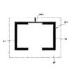
図1は、第1実施形態の液晶表示装置を構成する表示パネルの平面図である。この表示パネル10は、厚さ方向において2枚のガラス板21、22の間に後述する高分子分散型液晶を挟んだものである。矩形の視野領域IFの内部には、5つの表示パターン(「[ ]」状部分)DP1〜DP5が適宜配列されている。各表示パターンDP1〜DP5と、これらにそれぞれ結線された配線パターンWP1〜WP5とは、表面側の第2ガラス板22の内面側に形成されたものであり、各配線パターンWP1〜WP5の他端は、表示パネル10の一辺に向かって延びている。この辺には、裏面側の第1ガラス板21をはみ出させることによって段差が形成されている。この段差における第1ガラス板21側の表面には、端子引出部31が形成されている。
【0012】
端子引出部31には、一定ピッチで端子T1〜T5が形成されている。端子T1〜T5は、配線パターンWP1〜WP5にそれぞれ接続されている。この端子引出部31には、ゼブラと称される、絶縁層と導電層とを薄く多層に積層したゴム状体や、フレキシブルケーブルを圧着する。これにより、外部に設けた駆動回路(後述)からの給電用の電線を適宜各端子T1〜T5を介してそれぞれの配線パターンWP1〜WP5に接続することができる。
【0013】
なお、第2ガラス板22の内面において、表示パターンDP1〜DP5及び配線パターンWP1〜WP5の周囲には、僅かな隙間を介して背景パターン(図示を省略)が形成されている。また、第2ガラス板22に対向する第1ガラス板21の内面側には、面全体にわたり一様に裏面電極32(図2に示す)が形成されている。前者の背景パターンには、上記の端子引出部31に設けた端子TBが接続されており、後者の裏面電極32には、端子引出部31に設けた端子TRが接続されている。
【0014】
図2は、図1の表示パネルの断面構造を示す。図からも明らかなように、この表示パネル10は、高分子分散型液晶50を第1ガラス板21と第2ガラス板22との隙間に注入した構造となっており、高分子分散型液晶50と第1ガラス板21との間、及び高分子分散型液晶50と第2ガラス板22との間には、ITO(インジウム・スズ・酸化物)からなる非常に薄い透明電極層32、42がそれぞれ形成されている。
【0015】
上側の透明電極層42は、図1に示す表示パターンDP1〜DP5と、配線パターンWP1〜WP5と、これらの周囲に設けられる背景パターンとのいずれかに相当する。すなわち、透明電極層42は表示パターンDP1〜DP5、配線パターンWP1〜WP5及び上記背景パターンにより構成されている。一方、下側の透明電極層32は、上記全パターンに対向して一様に設けられる共通の裏面電極に相当する。
【0016】
高分子分散型液晶50は、ネマチック液晶を高分子中に分散させた高分子・液晶複合材料からなり、電界効果によって液晶の屈折率を変化させて光の散乱度を変化させるものである。ここで、一対の透明電極層32、42にほぼゼロの電圧を印加する場合、高分子分散型液晶50は、電界が加えられていない光散乱状態となって白濁する。一方、一対の透明電極層32、42に所定以上の電圧を印加する場合、高分子分散型液晶50は、電界が加えられた状態となって高い光透過性を示す。
【0017】
なお、高分子分散型液晶50の厚みは10μm程度以下であり、また透明電極層32、42は数十nmであり、数百μmにもおよぶガラス板21、22の厚みに比べると非常に薄くなっている。
【0018】
図3は、透明電極層の境界における表示状態を説明する図である。図3(a)は、表示パターンと背景パターンとの境界を示し、図3(b)は、配線パターンと背景パターンとの境界を示す。
【0019】
図3(a)の場合、第2ガラス板22側の透明電極層42は、表示パターンDP1と、背景パターンBPとから成る。両パターンDP1、BPの間隙部分には、これらと厚さや屈折率が等しく透明な絶縁物質層33が設けられている。表示パターンDP1を設けた表示領域では、表示パターンDP1に電圧を印加することにより、高分子分散型液晶50は透明となって非表示状態となる。また、背景パターンBPを設けた背景領域では、背景パターンBPに電圧を印加することにより、高分子分散型液晶50は透明となって入射光束(像光)を透過させる。両パターンDP1、BPともに電圧を印加した場合、絶縁物質層33を設けた境界部分では、高分子分散型液晶50に周囲からの電界が回り込むと考えられる。この結果、境界部分の高分子分散型液晶50も透明となって、表示パネル10の視野領域全体が入射光束を透過させる。つまり、表示パターンDP1が透明となって非表示状態にあるとき、表示パターンDP1と背景パターンBPの境界部分、すなわち表示パターンDP1の輪郭が表示されるといった不都合が生じない。このように絶縁物質33を設けた境界部分の幅は、表示パタ−ンDP1と背景パターンBPに電圧を印加した場合、この境界部分に対向する高分子分散型液晶層50に周囲からの電界が廻り込んで境界部分を透明にする程度のものであり、具体的には両パターンの間の境界部分の幅が高分子分散型液晶層50の膜厚にほぼ等しい。ここでほぼ等しいとは高分子分散型液晶層50の膜厚の2倍程度以下であることを意味する。現実の液晶表示装置では、高分子分散型液晶層50の厚みが10μm程度であるので、両パターンの間隔は、最大でも20μm以下にする必要がある。
【0020】
一方、表示パターンDP1に電圧を印加しない場合、すなわち表示パターンDP1への給電を遮断してハイインピーダンス状態とする場合、表示領域では高分子分散型液晶50が白濁して光散乱状態となり白地領域として表示される。この際、境界領域のみならず表示領域の縁部分にも背景パターンBPからの電界が回り込むことになるが、表示の見え方にはほとんど影響しない。
【0021】
図3(b)の場合、第2ガラス板22側の透明電極層42は、配線パターンWP1と、背景パターンBPとから成る。両パターンWP1、BPの間隔部分には、これらと厚さや屈折率が等しく透明な絶縁物質層33が設けられている。背景パターンBPを設けた背景領域では、既述のように背景パターンBPに電圧を印加することにより、高分子分散型液晶50は透明となって入射光束を透過させる。また、配線パターンWP1を設けた配線領域では、配線パターンWP1に電圧を印加することにより、高分子分散型液晶50が透明となって入射光束を透過させる。両パターンWP1、BPに電圧を印加した場合、絶縁物質層33を設けた境界部分では、高分子分散型液晶50に周囲からの電界が廻り込み、境界部分の高分子分散型液晶50も透明となって、表示パネル10の視野領域全体が入射光束を透過させる。つまり、表示パターンDP1とともに配線パターンWP1も透明となって非表示状態にあるとき、配線パターンWP1と背景パターンBPの境界部分、すなわち配線パターンWP1の輪郭が表示されるといった不都合が生じない。
【0022】
一方、配線パターンWP1に電圧を印加しない場合、すなわち表示パターンDP1への給電を遮断してハイインピーダンス状態とする場合、配線領域(例えば幅5μm)とこれを挟む境界部分(各領域、例えば幅7μm)では、これら部分に対向する高分子分散型液晶50に周囲の背景領域からの電界が廻り込んで透明となる。つまり、表示パターンDP1を表示状態とした場合に、配線領域の表示を消すことができる。このように、本実施形態において、配線パターンWP1を挟む両側の境界部分33、33と配線パターンWP1との合計幅は、この合計幅部分に対向する高分子分散型液晶層50が、周囲の背景パターンBPからの電界により透明化するに十分にされており、上記合計幅は高分子分散型液晶層50の厚さとほぼ等しくされている。ここで、ほぼ等しいとは合計幅が高分子分散型液晶層50の2倍程度以下であることを意味する。
【0023】
なお、以上において、表示パターンDP1と、背景パターンBPと、配線パターンWP1は、第2ガラス板22上へのITOの蒸着後に不要部分をエッチングすることによって形成され、エッチングにより形成された隙間には、適当な方法で絶縁物質層33が埋め込まれる。
【0024】
図4は、一表示パターンの形状を説明する拡大平面図である。図示の表示パターンDP1は、一対のセグメントS1、S2から構成される。両セグメントS1、S2は、分岐する配線パターンWP1の先端に接続されている。なお、図面ではデフォルメしてあるが、実際には各セグメントS1、S2の幅は約100μmとなっており、幅5μm程度の配線パターンWP1に比べて非常に太くなっている。
【0025】
図5は、図1に示す表示パネルに設けた各パターンの表示状態を制御する駆動回路の要部を説明する図である。この駆動回路は、インバータやスリーステートバッファ等のデジタル回路素子からなり、裏面の透明電極層32(図3参照)を駆動するための裏面ドライブ部61、背景パターンBP(図3参照)を駆動するための背景ドライブ部62と、表示パターンDP1〜DP5(図1、3参照)を駆動するための表示ドライブ部63とを備える。
【0026】
基準となるクロック信号CKとしては、例えば比較的周波数の低い50HZの矩形波を用いる。高分子分散型液晶50の裏面側に配置される透明電極層32には、裏面ドライブ部61の出力に接続された端子TRを介して、上記クロック信号CKを反転した逆相信号が印加される。高分子分散型液晶50の表面側に配置される背景パターンBPには、背景ドライブ部62の出力に接続された端子TBを介して、裏面ドライブ部61の出力に接続された端子TRと同位相の信号と、これに対して逆位相つまりπだけ位相のずれた信号とのいずれかが印加される。これら同相信号と逆相信号の切り替えは、背景ドライブ部62を構成するスリーステートバッファの制御入力端子BSへの印加信号によって任意に行い得るようになっている。高分子分散型液晶50の表面側に配置される表示パターンDP1〜DP5には、表示ドライブ部63の出力に接続された端子T1、T2、T3、…を介して、電圧が印加されたたり電圧の印加が遮断される。これにより、表示パターンDP1〜DP5は、裏面ドライブ部61の出力に接続された端子TRと逆位相の信号を印加する状態と、信号ラインの接続を断って端子T1、T2、T3、…の各ラインを電気的に浮かしてしまうハイインピーダンス状態との切り替えが可能になる。これら逆相信号の印加状態とハイインピーダンス状態との切り替えは、表示ドライブ部63を構成するスリーステートバッファの制御入力端子DS1、DS2、DS3、…への印加信号によって、各表示パターンDP1〜DP5に個別に行い得るようになっている。
【0027】
まず、背景ドライブ部62の出力に注目する。端子TBを介して背景パターンBPに裏面側の端子TRとは逆位相の信号が印可されると、背景パターンBPと透明電極層32との間には交流電界が生じ、これによって高分子分散型液晶50を構成する液晶の分子が整列して、この部分(背景領域)は透明化する。これで、表示パネル10の表示部分の大半をしめる背景領域が透明化され、表示パネル10の片面から反対面へと抜ける入射光束がここを通過できることになる。
【0028】
次に、表示ドライブ部63の出力に注目する。端子T1、T2、T3、…を介して表示パターンDP1〜DP5のいずれかに裏面側の端子TRとは逆位相の信号が印可されると、上記バックグラウンドと同様に、表示パターンDP1〜DP5のいずれかに相当する部分(表示領域)は透明化する。
【0029】
ここで、表示ドライブ部63の出力端子への電圧供給を遮断する場合、結果として端子T1、T2、T3、…がハイインピーダンス状態となる。
【0030】
表示パターンDP1〜DP5および配線パターンWP1〜WP5からなるパターン電極の線幅が細いとき、例えば幅5μm以下になるときには、高分子分散型液晶50の膜厚が先に述べたように10μm程度であるから、線幅とその両側の境界領域の幅との合計幅が高分子分散型液晶50の膜厚と同等程度になるため、上記パターン電極の周りの背景パターン電極の電界が上記細い線幅のパターン電極とその両側の境界領域との合計幅領域直下の高分子分散型液晶50に廻り込む。そして、この合計幅領域部分の高分子分散型液晶50に電界の効果を発生させ、この部分の液晶を整列させ、高分子分散型液晶50の特性から透明化する。すなわち、ハイインピーダンス状態となったパターン電極の線幅が細いとき、具体的には配線パターンWP1〜WP5の部分では、これらパターン及び隣接した境界部分が透明化する。
【0031】
一方、上記パターン電極の線幅が太いとき、例えば数百μm以上となるときには、パターン電極は隣よりもむしろ対面する透明電極層32の信号に誘導され、この透明電極層32と同位相になる傾向が強くなると同時に電界の廻り込みの影響が小さくなくなるので、パターン電極直下の高分子分散型液晶50に電界の効果は発生せず、高分子分散型液晶50が光散乱状態となる。すなわち、ハイインピーダンス状態となったパターン電極の線幅が太いとき、具体的には表示パターンDP1〜DP5の部分では、これらが透明の背景領域に対して白地領域として表示されることになる。
【0032】
図6は、図1に示す表示パネルを組み込んだ一眼レフレックスカメラの構造を概念的に説明する図である。
【0033】
この一眼レフレックスカメラは、被写体の像をフィルム上に結像させるための撮影レンズ2と、撮影レンズ2からの光の光路を切り換えるための跳ね上げ式の反射ミラー3と、フィルムと共役な面に配置されるスクリーン4と、このスクリーン4に近接して配置される表示パネル10と、スクリーン4及び表示パネル10を透過した光を観察のために折り曲げるペンタプリズム5と、スクリーン4上に投影された像を観察するためのレンズ6と、表示パネル10を駆動する駆動回路7とを備える。
【0034】
表示パネル10は、図1〜図4に示す構造を有しており、図5に示す構造を有する駆動回路7によって駆動される。なお、駆動回路7は、一眼レフレックスカメラの動作を統括的に制御するCPU8からの指示に基づいて動作する。CPU8は、図示を省略するAE装置やAF装置等からの信号に基づき、駆動回路7を介して表示パネル10の表示状態を制御する。
【0035】
図示のように、表示パネル10をスクリーン4に近接して配置すると、撮影レンズ2によってスクリーン4に結像した像は、この表示パネル10のバックグランド(背景領域)をそのまま通過する。また、表示パネル10のバックグランド以外の部分、つまり表示パターンDP1〜DP5の部分がハイインピーダンス状態となって光散乱状態となったときは、この部分に入射する光は、すべての方向に散乱されて、目の方向に行く光はごく一部だけとなる。必然的にこの部分の光量は下がり表示される部分がそのほかに比べて暗く沈むことになる。こうした効果によって、この表示パネル10で光学的に背景と表示パターンとがスーパーインポーズされることになる。なお、スクリーン4に十分な光が到達しない場合、表示パネル10の縁側の側面から適当な光量の照明光を入射させることにより、暗い背景中に明るい表示パターンがスーパーインポーズされることになる。
【0036】
以上から明らかなように、本実施形態の表示パネル10では、配線部分の幅とパターンを構成する隣接セグメントの間の両間隙部(境界部)とを背景領域の電界の廻り込みにより透明化するのに十分なだけ細くするとともに、表示パターンDP1〜DP5を構成するセグメントについては背景領域の電界の廻り込みがあっても光散乱状態が維持される程度以上に太い線幅にしてあるので、表示パターンDP1〜DP5をハイインピーダンス状態にすると配線パターンWP1〜WP5は透明化して見えず表示パターンDP1〜DP5を構成するセグメントだけが白地領域として表示されることになる。また、表示パターンDP1〜DP5に裏面の透明電極層32とは逆位相の信号を加えて透明化させたときにも、表示パターンDP1〜DP5と背景パターンBPとの隙間を十分に小さくとっているので、電極のない部分であるこの間隙部に対向する高分子分散型液晶50領域にも上記と同様の効果で電界が廻り込み、高分子分散型液晶50が透明化し、各表示パターンDP1〜DP5の縁取りが観測されなくなる。
【0037】
〔第2実施形態〕
図7は、第2実施形態の液晶表示装置を構成する表示パネルの平面図である。なお第2実施形態の液晶表示装置は、第1実施形態の液晶表示装置の変形例であり、同一部分には同一の符号を付して重複説明を省略する。
【0038】
この表示パネル110の視野領域IFの内部には、図1と同様に5つの表示パターンDP1〜DP5が配列されている。各表示パターンDP1〜DP5は、「[ 」状のセグメントと、「 ]」状のセグメントとからなっており、これらのセグメントには、配線パターンWP11〜WP52が個別に接続されている。つまり、図1の配線パターンWP1は図7のWP11、WP12に相当し、配線パターンWP2はWP21、WP22に相当し、配線パターンWP3はWP31、WP32に相当し、配線パターンWP4はWP41、WP42に相当し、配線パターンWP5はWP51、WP52に相当する。
【0039】
そして、端子引出部31には、端子T11〜T52、TB、TRが形成される。ここで、図1の端子T1は図7の端子T11、T12に相当し、端子T2は端子T21、T22に相当し、端子T3は端子T31、T32に相当し、端子T3は端子T41、T42に相当し、端子T4は端子T41、T42に相当する。
【0040】
この場合、各表示パターンDP1〜DP5に給電する配線が増えることになるが、表示パターンDP1〜DP5の駆動は、図5に示す駆動回路とほぼ同様の回路によって達成できる。
【0041】
〔第3実施形態〕
図8は、第3実施形態の液晶表示装置を構成する表示パネルの平面図である。なお第3実施形態の液晶表示装置は、第1実施形態の液晶表示装置の変形例である。
【0042】
この表示パネル210の視野領域IFの内部には、格子状の表示パターンDP201が形成されており、この表示パターンDP201には、周囲から複数の配線パターンWP201〜WP209が接続されている。そして、端子引出部31には、端子T201〜T209、TB、TRが形成される。
【0043】
この場合、表示パターンDP201の面積が比較的大きくなるが、複数の配線パターンWP201〜WP209から電圧を供給しているので、位相遅れ等の弊害がなく所望の表示を達成できる。
【0044】
以上、実施形態に即して本発明を説明したが、本発明は、上記実施形態に限定されるものではない。例えば、表示パターンの形状や大きさは、表示パネルの使用目的等に応じて適宜変更することができる。
【0045】
また、上記実施形態では、表示パターンDP1〜DP5をスリーステートバッファを利用してデジタル的に駆動することによってハイインピーダンス状態としているが、表示パターンDP1〜DP5の表示・非表示をアナログ的に制御することもできる。この場合、FETで構成されるアナログスイッチより、表示パターンDP1〜DP5に裏面側の透明電極層32と逆位相の正弦波を接続したり、表示パターンDP1〜DP5への電圧供給ラインを切り離したりすることもできる。また、スリーステートバッファやFETの代わりに、機械的にリレーを使用して回路の接続と切り離しを行うこともできる。
【0046】
【発明の効果】
以上の説明から明らかなように、本発明の液晶表示装置によれば、第1電極パターンと第2電極パターンとに電圧を印加することによって両パターンが共に透明状態となった場合、両パターンの境界部分に対向する高分子分散型液晶層に周囲からの電界が回り込んで、両隣接パターンの境界部分が表示・観察されなくなる。つまり、カメラその他の光学装置において、意図したままの表示内容を光学的にスーパーインポーズすることができるようになる。
【図面の簡単な説明】
【図1】第1実施形態の液晶表示装置を構成する表示パネルの平面図である。
【図2】図1の表示パネルの断面構造を示す図である。
【図3】(a)(b)は、透明電極層の境界における表示状態を説明する図である。
【図4】表示パターンの形状を説明する拡大平面図である。
【図5】図1に示す表示パネルの駆動回路を説明する図である。
【図6】図1の表示パネルや図5の駆動回路を組み込んだカメラの構造を説明する図である。
【図7】第2実施形態の液晶表示装置を構成する表示パネルの平面図である。
【図8】第3実施形態の液晶表示装置を構成する表示パネルの平面図である。
【符号の説明】
2 撮影レンズ
3 反射ミラー
4 スクリーン
5 ペンタプリズム
7 駆動回路
10 表示パネル
21 第1ガラス板
22 第2ガラス板
32,42 透明電極層
50 高分子分散型液晶
61 裏面ドライブ部
62 背景ドライブ部
63 表示ドライブ部
BP 背景パターン
DP1〜DP5 表示パターン
T1〜T5,TB,TR 端子
WP1〜WP5 配線パターン[0001]
BACKGROUND OF THE INVENTION
The present invention relates to a liquid crystal display device using a polymer dispersed liquid crystal.
[0002]
[Prior art]
In a liquid crystal display device that performs efficient operation using a polymer-dispersed liquid crystal, the liquid crystal is usually in a non-transparent state (light scattering state) by non-energization, and the liquid crystal is in a transparent state by energization. The display is made using it. More specifically, in the liquid crystal display device as described above, the polymer-dispersed liquid crystal is disposed between the opposing transparent electrodes. The liquid crystal is in a light scattering state in which no voltage is applied by applying an in-phase AC signal to both transparent electrodes, and a transparent state in which a voltage is applied by applying an AC signal having a different phase to both transparent electrodes. Become. When the liquid crystal is driven in this way, it is possible to display a transparent area on a white background such as frosted glass by making the pattern transparent and surrounding the light scattering state, or by making the pattern light scattering and transparent the surroundings. By setting the state, the white area is displayed on the transparent background.
[0003]
[Problems to be solved by the invention]
As long as a transparent body is displayed on a white background, there is no particular problem with the above apparatus configuration. However, the following problems arise when trying to display a white background area on a transparent background.
[0004]
Consider a display area like an island floating in a transparent background. In such a case, even if a voltage is applied to the background area around the display area to make it a transparent background, a wiring portion reaching the display area becomes a problem. That is, if the island-shaped display region is not energized, that is, if the voltage applied between both electrodes is in the same phase, naturally, the wiring portion leading to it has the same phase potential as the opposing transparent electrode. This means that if the island-shaped display area is displayed in a light scattering state, the wiring portion reaching the display area is also in a light scattering state and is displayed at the same time.
[0005]
In a liquid crystal display device, displaying an island-shaped white background area in a transparent background means that when a liquid crystal display plate is incorporated in an optical system, an image of a light beam transmitted by a transparent body is displayed. This is so-called superimposing and displaying the display mark so as to emerge as a white background area. In this case, since a wiring for supplying a voltage to the display mark is connected to the display mark, a voltage is applied to the liquid crystal via the wiring, and all of the segments constituting the display mark extend from the edge of the screen. Corresponding to the above, it will look like a string, and the transmitted light flux image will be ruined.
[0006]
Furthermore, the boundary between the background portion and the display mark includes a boundary between segments constituting the transparent electrode corresponding to both, and this boundary remains as a blank portion where no electrode pattern exists. In this blank portion, an electric field is not applied to the liquid crystal region that is opposed to the blank portion, so that the light scattering state is always maintained. In other words, the content displayed when the background part is transparent and the display mark part is also transparent, the blank part is displayed as a white background area like the border of the display mark, and blank when the display mark part is white Both the part and the display mark part become a display mark filled as a white background area.
[0007]
As described above, in the conventional liquid crystal display device, even when the display mark is unnecessary, it cannot be completely erased, and the display restriction that the wiring portion blinks each time the display mark blinks. Exists. Such a restriction is a major obstacle in optically superimposing a desired display on the background image. In other words, it is desirable that the display to be superimposed is not simply displayed, but completely disappears when unnecessary.
[0008]
Therefore, the present invention can superimpose a desired display on the background image while preventing the inconvenience of displaying the wiring portion to the display mark or displaying only the border of the display mark. An object is to provide a liquid crystal display device.
[0009]
[Means for Solving the Problems]
In order to solve the above-described problems, a liquid crystal display device according to the present invention includes a polymer dispersed liquid crystal layer that is in a light scattering state when no voltage is applied, and a first and a second that form an electric field in the polymer dispersed liquid crystal layer. The first transparent electrode has a first electrode pattern and a second electrode pattern disposed adjacent to the first electrode pattern via a boundary portion; The first electrode pattern has a display pattern and a wiring pattern, the second electrode pattern is a background pattern, The width of the boundary portion is sufficient to make the portion of the polymer dispersed liquid crystal layer corresponding to the boundary portion transparent by the action of an electric field formed by the second electrode pattern and the second transparent electrode. It is characterized by its size.
[0010]
According to the present invention, in the above-described apparatus, when both patterns become transparent by applying a voltage to the first electrode pattern and the second electrode pattern, the polymer in the region facing the boundary between both patterns The electric field from the surroundings wraps around the dispersed liquid crystal layer, and the boundary between the two patterns is not displayed or observed.
[0011]
DETAILED DESCRIPTION OF THE INVENTION
[First Embodiment]
FIG. 1 is a plan view of a display panel constituting the liquid crystal display device of the first embodiment. The
[0012]
Terminals T1 to T5 are formed in the
[0013]
Note that a background pattern (not shown) is formed on the inner surface of the
[0014]
FIG. 2 shows a cross-sectional structure of the display panel of FIG. As is apparent from the figure, the
[0015]
The upper
[0016]
The polymer-dispersed
[0017]
The thickness of the polymer dispersed
[0018]
FIG. 3 is a diagram illustrating a display state at the boundary of the transparent electrode layer. FIG. 3A shows the boundary between the display pattern and the background pattern, and FIG. 3B shows the boundary between the wiring pattern and the background pattern.
[0019]
In the case of FIG. 3A, the
[0020]
On the other hand, when a voltage is not applied to the display pattern DP1, that is, when the power supply to the display pattern DP1 is cut off to be in a high impedance state, the polymer dispersed
[0021]
In the case of FIG. 3B, the
[0022]
On the other hand, when no voltage is applied to the wiring pattern WP1, that is, when the power supply to the display pattern DP1 is cut off and a high impedance state is established, the wiring region (for example,
[0023]
In the above, the display pattern DP1, the background pattern BP, and the wiring pattern WP1 are formed by etching unnecessary portions after ITO is deposited on the
[0024]
FIG. 4 is an enlarged plan view for explaining the shape of one display pattern. The illustrated display pattern DP1 includes a pair of segments S1 and S2. Both segments S1, S2 are connected to the tip of the branched wiring pattern WP1. Although it is deformed in the drawing, the width of each segment S1, S2 is actually about 100 μm, which is much thicker than the wiring pattern WP1 having a width of about 5 μm.
[0025]
FIG. 5 is a diagram for explaining a main part of a drive circuit for controlling the display state of each pattern provided on the display panel shown in FIG. This drive circuit is composed of digital circuit elements such as an inverter and a three-state buffer, and drives the back
[0026]
As the reference clock signal CK, for example, a 50 Hz rectangular wave having a relatively low frequency is used. A reverse phase signal obtained by inverting the clock signal CK is applied to the
[0027]
First, attention is focused on the output of the
[0028]
Next, attention is focused on the output of the
[0029]
Here, when the voltage supply to the output terminal of the
[0030]
When the line width of the pattern electrode composed of the display patterns DP1 to DP5 and the wiring patterns WP1 to WP5 is thin, for example, when the width is 5 μm or less, the film thickness of the polymer dispersed
[0031]
On the other hand, when the line width of the pattern electrode is large, for example, when it is several hundred μm or more, the pattern electrode is induced by the signal of the
[0032]
6 is a diagram conceptually illustrating the structure of a single-lens reflex camera incorporating the display panel shown in FIG.
[0033]
This single-lens reflex camera includes a photographing
[0034]
The
[0035]
As shown in the figure, when the
[0036]
As is clear from the above, in the
[0037]
[Second Embodiment]
FIG. 7 is a plan view of a display panel constituting the liquid crystal display device of the second embodiment. Note that the liquid crystal display device of the second embodiment is a modification of the liquid crystal display device of the first embodiment, and the same portions are denoted by the same reference numerals and redundant description is omitted.
[0038]
Within the visual field area IF of the
[0039]
In the
[0040]
In this case, the number of wirings for supplying power to each of the display patterns DP1 to DP5 increases, but the driving of the display patterns DP1 to DP5 can be achieved by a circuit that is substantially the same as the drive circuit shown in FIG.
[0041]
[Third Embodiment]
FIG. 8 is a plan view of a display panel constituting the liquid crystal display device of the third embodiment. The liquid crystal display device of the third embodiment is a modification of the liquid crystal display device of the first embodiment.
[0042]
A lattice-shaped display pattern DP201 is formed inside the visual field area IF of the
[0043]
In this case, although the area of the display pattern DP201 is relatively large, since a voltage is supplied from the plurality of wiring patterns WP201 to WP209, a desired display can be achieved without any adverse effects such as phase delay.
[0044]
As described above, the present invention has been described according to the embodiment, but the present invention is not limited to the above embodiment. For example, the shape and size of the display pattern can be appropriately changed according to the purpose of use of the display panel.
[0045]
In the above embodiment, the display patterns DP1 to DP5 are in a high impedance state by digitally driving using a three-state buffer, but display / non-display of the display patterns DP1 to DP5 is controlled in an analog manner. You can also. In this case, a sine wave having a phase opposite to that of the
[0046]
【The invention's effect】
As is clear from the above description, according to the liquid crystal display device of the present invention, when both patterns become transparent by applying a voltage to the first electrode pattern and the second electrode pattern, The electric field from the periphery wraps around the polymer-dispersed liquid crystal layer facing the boundary portion, and the boundary portion between both adjacent patterns is not displayed or observed. That is, the intended display content can be optically superimposed on the camera or other optical device.
[Brief description of the drawings]
FIG. 1 is a plan view of a display panel constituting a liquid crystal display device according to a first embodiment.
2 is a view showing a cross-sectional structure of the display panel of FIG. 1;
FIGS. 3A and 3B are diagrams illustrating a display state at a boundary of a transparent electrode layer.
FIG. 4 is an enlarged plan view illustrating the shape of a display pattern.
5 is a diagram illustrating a drive circuit for the display panel shown in FIG. 1. FIG.
6 is a diagram illustrating a structure of a camera in which the display panel of FIG. 1 and the driving circuit of FIG. 5 are incorporated.
FIG. 7 is a plan view of a display panel constituting the liquid crystal display device of the second embodiment.
FIG. 8 is a plan view of a display panel constituting a liquid crystal display device of a third embodiment.
[Explanation of symbols]
2 Photo lens
3 Reflection mirror
4 screens
5 Penta prism
7 Drive circuit
10 Display panel
21 First glass plate
22 Second glass plate
32, 42 Transparent electrode layer
50 Polymer dispersed liquid crystal
61 Rear drive section
62 Background drive section
63 Display drive section
BP background pattern
DP1 to DP5 display pattern
T1-T5, TB, TR terminals
WP1-WP5 wiring pattern
Claims (9)
前記高分子分散型液晶層に電界を形成する第1および第2の透明電極とを備え、
第1の透明電極は第1電極パターンと該第1電極パターンに境界部分を介して隣接配置された第2電極パターンとを有し、
前記第1電極パターンは表示パターンと配線パターンを有し、前記第2電極パターンは背景パターンであり、
該境界部分の幅は、前記第2電極パターンと前記第2の透明電極とにより形成される電界の作用により前記境界部分に対応する前記高分子分散型液晶層の部分を透明化するに十分な大きさであることを特徴とする液晶表示装置。A polymer-dispersed liquid crystal layer that enters a light scattering state when no voltage is applied;
Comprising first and second transparent electrodes for forming an electric field in the polymer dispersed liquid crystal layer,
The first transparent electrode has a first electrode pattern and a second electrode pattern disposed adjacent to the first electrode pattern via a boundary portion;
The first electrode pattern has a display pattern and a wiring pattern, the second electrode pattern is a background pattern,
The width of the boundary portion is sufficient to make the portion of the polymer dispersed liquid crystal layer corresponding to the boundary portion transparent by the action of an electric field formed by the second electrode pattern and the second transparent electrode. A liquid crystal display device having a size.
前記表示パターンと前記配線パターンは複数は位置され、
それぞれの前記配線パターンの一端は複数の前記表示パターンのいずれかに結線され、それぞれの前記配線パターンの他端は、前記矩形の一辺に向かって延びていることを特徴とする請求項4から6のいずれか一項に記載の液晶表示装置。The polymer dispersed liquid crystal layer is formed in a rectangular shape,
A plurality of the display pattern and the wiring pattern are positioned,
7. One end of each of the wiring patterns is connected to one of the plurality of display patterns, and the other end of each of the wiring patterns extends toward one side of the rectangle. The liquid crystal display device according to any one of the above.
Priority Applications (2)
| Application Number | Priority Date | Filing Date | Title |
|---|---|---|---|
| JP2000387282A JP4649736B2 (en) | 2000-01-19 | 2000-12-20 | Liquid crystal display |
| US09/760,751 US6493049B2 (en) | 2000-01-19 | 2001-01-17 | PDLC display device including first electrode pattern and second electrode pattern disposed adjoiningly to the first via a boundary area |
Applications Claiming Priority (3)
| Application Number | Priority Date | Filing Date | Title |
|---|---|---|---|
| JP2000010963 | 2000-01-19 | ||
| JP2000-10963 | 2000-01-19 | ||
| JP2000387282A JP4649736B2 (en) | 2000-01-19 | 2000-12-20 | Liquid crystal display |
Publications (3)
| Publication Number | Publication Date |
|---|---|
| JP2001272690A JP2001272690A (en) | 2001-10-05 |
| JP2001272690A5 JP2001272690A5 (en) | 2008-05-08 |
| JP4649736B2 true JP4649736B2 (en) | 2011-03-16 |
Family
ID=26583808
Family Applications (1)
| Application Number | Title | Priority Date | Filing Date |
|---|---|---|---|
| JP2000387282A Expired - Fee Related JP4649736B2 (en) | 2000-01-19 | 2000-12-20 | Liquid crystal display |
Country Status (2)
| Country | Link |
|---|---|
| US (1) | US6493049B2 (en) |
| JP (1) | JP4649736B2 (en) |
Families Citing this family (7)
| Publication number | Priority date | Publication date | Assignee | Title |
|---|---|---|---|---|
| WO2005022244A1 (en) * | 2003-08-28 | 2005-03-10 | Koninklijke Philips Electronics N.V. | Lateral ion pumping in liquid crystal displays |
| JP2007316484A (en) * | 2006-05-29 | 2007-12-06 | Pentax Corp | Transmissive display device, and camera |
| CA2564461A1 (en) | 2006-10-17 | 2008-04-17 | Ibm Canada Limited - Ibm Canada Limitee | Double-sided lcd panel |
| US20110200314A1 (en) * | 2008-08-12 | 2011-08-18 | Optoelectronics Co. Ltd. | Liquid lens with temperature compensated focus time |
| JP2011059582A (en) * | 2009-09-14 | 2011-03-24 | Sony Corp | Imaging device |
| TWM423259U (en) * | 2011-08-09 | 2012-02-21 | Chunghwa Picture Tubes Ltd | Liquid crystal display component and light guide plate thereof |
| US9383666B1 (en) | 2015-04-01 | 2016-07-05 | Xerox Corporation | Toner particles comprising both polyester and styrene acrylate polymers having a polyester shell |
Citations (3)
| Publication number | Priority date | Publication date | Assignee | Title |
|---|---|---|---|---|
| JPH04131893A (en) * | 1990-09-21 | 1992-05-06 | Sharp Corp | Liquid crystal display device |
| JPH05196921A (en) * | 1992-01-17 | 1993-08-06 | Aronshiya:Kk | Image display device |
| JP2000347205A (en) * | 1999-06-02 | 2000-12-15 | Nikon Corp | Liquid crystal display device |
Family Cites Families (3)
| Publication number | Priority date | Publication date | Assignee | Title |
|---|---|---|---|---|
| US5583671A (en) * | 1992-11-09 | 1996-12-10 | Casio Computer Co., Ltd. | Method of manufacturing polymer dispersed liquid crystal display devices |
| US6166834A (en) * | 1996-03-15 | 2000-12-26 | Matsushita Electric Industrial Co., Ltd. | Display apparatus and method for forming hologram suitable for the display apparatus |
| US6421109B1 (en) * | 1998-10-16 | 2002-07-16 | Digilens, Inc. | Method and system for display resolution multiplication |
-
2000
- 2000-12-20 JP JP2000387282A patent/JP4649736B2/en not_active Expired - Fee Related
-
2001
- 2001-01-17 US US09/760,751 patent/US6493049B2/en not_active Expired - Lifetime
Patent Citations (3)
| Publication number | Priority date | Publication date | Assignee | Title |
|---|---|---|---|---|
| JPH04131893A (en) * | 1990-09-21 | 1992-05-06 | Sharp Corp | Liquid crystal display device |
| JPH05196921A (en) * | 1992-01-17 | 1993-08-06 | Aronshiya:Kk | Image display device |
| JP2000347205A (en) * | 1999-06-02 | 2000-12-15 | Nikon Corp | Liquid crystal display device |
Also Published As
| Publication number | Publication date |
|---|---|
| US20010009448A1 (en) | 2001-07-26 |
| US6493049B2 (en) | 2002-12-10 |
| JP2001272690A (en) | 2001-10-05 |
Similar Documents
| Publication | Publication Date | Title |
|---|---|---|
| JP7349469B2 (en) | display device | |
| JP5862018B2 (en) | Display element, display element control method, and image display system | |
| US7929098B2 (en) | Liquid crystal display element, display device, observation device, camera, and method for manufacturing liquid crystal display element | |
| EP2390718A1 (en) | Active matrix substrate, liquid crystal display panel, liquid crystal display device, method for manufacturing active matrix substrate, method for manufacturing liquid crystal display panel and method for driving liquid crystal display panel | |
| JP5241822B2 (en) | Display panel and camera | |
| JP2008544312A (en) | Bistable display device | |
| JP4649736B2 (en) | Liquid crystal display | |
| JPH0434348B2 (en) | ||
| JPH0643478A (en) | Liquid crystal display device | |
| JP5136636B2 (en) | Display device and camera | |
| TWI428881B (en) | Polymer network liquid crystal driving apparatus and driving method, and polymer network liquid crystal panel | |
| JP5927057B2 (en) | Liquid crystal display | |
| JP2018146697A (en) | Display device | |
| US11796869B2 (en) | Device with imaging unit | |
| JP2017142328A (en) | Display | |
| CN109814248A (en) | Display device and its control method | |
| JP4378800B2 (en) | Display device and camera equipped with the display device | |
| CN114675441A (en) | Display panel with switchable wide and narrow viewing angles and regions, driving method and display device | |
| JP5505442B2 (en) | Display device and camera | |
| JP2001013499A (en) | Display device | |
| JP2008203711A (en) | Active matrix substrate, electro-optical device and electronic equipment | |
| JPH1048592A (en) | Finder display device and its driving method | |
| US11822165B1 (en) | Displays with adjustable angles of view | |
| JP2018146817A (en) | Liquid crystal display device and control method of the same | |
| JP2017142327A (en) | Display |
Legal Events
| Date | Code | Title | Description |
|---|---|---|---|
| A621 | Written request for application examination |
Free format text: JAPANESE INTERMEDIATE CODE: A621 Effective date: 20071030 |
|
| A521 | Request for written amendment filed |
Free format text: JAPANESE INTERMEDIATE CODE: A523 Effective date: 20080324 |
|
| A977 | Report on retrieval |
Free format text: JAPANESE INTERMEDIATE CODE: A971007 Effective date: 20100531 |
|
| A131 | Notification of reasons for refusal |
Free format text: JAPANESE INTERMEDIATE CODE: A131 Effective date: 20100622 |
|
| A521 | Request for written amendment filed |
Free format text: JAPANESE INTERMEDIATE CODE: A523 Effective date: 20100823 |
|
| TRDD | Decision of grant or rejection written | ||
| A01 | Written decision to grant a patent or to grant a registration (utility model) |
Free format text: JAPANESE INTERMEDIATE CODE: A01 Effective date: 20101116 |
|
| A01 | Written decision to grant a patent or to grant a registration (utility model) |
Free format text: JAPANESE INTERMEDIATE CODE: A01 |
|
| A61 | First payment of annual fees (during grant procedure) |
Free format text: JAPANESE INTERMEDIATE CODE: A61 Effective date: 20101129 |
|
| R150 | Certificate of patent or registration of utility model |
Ref document number: 4649736 Country of ref document: JP Free format text: JAPANESE INTERMEDIATE CODE: R150 Free format text: JAPANESE INTERMEDIATE CODE: R150 |
|
| FPAY | Renewal fee payment (event date is renewal date of database) |
Free format text: PAYMENT UNTIL: 20131224 Year of fee payment: 3 |
|
| FPAY | Renewal fee payment (event date is renewal date of database) |
Free format text: PAYMENT UNTIL: 20131224 Year of fee payment: 3 |
|
| R250 | Receipt of annual fees |
Free format text: JAPANESE INTERMEDIATE CODE: R250 |
|
| R250 | Receipt of annual fees |
Free format text: JAPANESE INTERMEDIATE CODE: R250 |
|
| R250 | Receipt of annual fees |
Free format text: JAPANESE INTERMEDIATE CODE: R250 |
|
| R250 | Receipt of annual fees |
Free format text: JAPANESE INTERMEDIATE CODE: R250 |
|
| R250 | Receipt of annual fees |
Free format text: JAPANESE INTERMEDIATE CODE: R250 |
|
| R250 | Receipt of annual fees |
Free format text: JAPANESE INTERMEDIATE CODE: R250 |
|
| LAPS | Cancellation because of no payment of annual fees |