JP4641741B2 - Semiconductor device - Google Patents
Semiconductor device Download PDFInfo
- Publication number
- JP4641741B2 JP4641741B2 JP2004159597A JP2004159597A JP4641741B2 JP 4641741 B2 JP4641741 B2 JP 4641741B2 JP 2004159597 A JP2004159597 A JP 2004159597A JP 2004159597 A JP2004159597 A JP 2004159597A JP 4641741 B2 JP4641741 B2 JP 4641741B2
- Authority
- JP
- Japan
- Prior art keywords
- region
- impurity region
- impurity
- channel
- thin film
- Prior art date
- Legal status (The legal status is an assumption and is not a legal conclusion. Google has not performed a legal analysis and makes no representation as to the accuracy of the status listed.)
- Expired - Fee Related
Links
- 239000004065 semiconductor Substances 0.000 title claims description 60
- 239000012535 impurity Substances 0.000 claims description 160
- 239000000758 substrate Substances 0.000 claims description 71
- VYPSYNLAJGMNEJ-UHFFFAOYSA-N silicon dioxide Inorganic materials O=[Si]=O VYPSYNLAJGMNEJ-UHFFFAOYSA-N 0.000 claims description 20
- 229910021420 polycrystalline silicon Inorganic materials 0.000 claims description 18
- 239000011521 glass Substances 0.000 claims description 12
- 239000010453 quartz Substances 0.000 claims description 2
- 239000010409 thin film Substances 0.000 description 165
- PCHJSUWPFVWCPO-UHFFFAOYSA-N gold Chemical compound [Au] PCHJSUWPFVWCPO-UHFFFAOYSA-N 0.000 description 145
- 239000010408 film Substances 0.000 description 87
- 239000004973 liquid crystal related substance Substances 0.000 description 45
- 229910052814 silicon oxide Inorganic materials 0.000 description 19
- 230000015556 catabolic process Effects 0.000 description 18
- OAICVXFJPJFONN-UHFFFAOYSA-N Phosphorus Chemical compound [P] OAICVXFJPJFONN-UHFFFAOYSA-N 0.000 description 14
- 229910052698 phosphorus Inorganic materials 0.000 description 14
- 239000011574 phosphorus Substances 0.000 description 14
- 239000010410 layer Substances 0.000 description 13
- 239000011229 interlayer Substances 0.000 description 11
- 238000000034 method Methods 0.000 description 11
- 239000003990 capacitor Substances 0.000 description 10
- 229910052581 Si3N4 Inorganic materials 0.000 description 8
- HQVNEWCFYHHQES-UHFFFAOYSA-N silicon nitride Chemical compound N12[Si]34N5[Si]62N3[Si]51N64 HQVNEWCFYHHQES-UHFFFAOYSA-N 0.000 description 8
- 230000008569 process Effects 0.000 description 7
- VYZAMTAEIAYCRO-UHFFFAOYSA-N Chromium Chemical compound [Cr] VYZAMTAEIAYCRO-UHFFFAOYSA-N 0.000 description 6
- 230000001133 acceleration Effects 0.000 description 6
- 229910021417 amorphous silicon Inorganic materials 0.000 description 6
- 229910052804 chromium Inorganic materials 0.000 description 6
- 239000011651 chromium Substances 0.000 description 6
- 238000004519 manufacturing process Methods 0.000 description 6
- 238000004380 ashing Methods 0.000 description 5
- 239000000126 substance Substances 0.000 description 5
- 238000001039 wet etching Methods 0.000 description 5
- 238000005530 etching Methods 0.000 description 4
- 238000002347 injection Methods 0.000 description 4
- 239000007924 injection Substances 0.000 description 4
- 238000003860 storage Methods 0.000 description 4
- 230000005684 electric field Effects 0.000 description 3
- 230000003071 parasitic effect Effects 0.000 description 3
- 238000000206 photolithography Methods 0.000 description 3
- XUIMIQQOPSSXEZ-UHFFFAOYSA-N Silicon Chemical compound [Si] XUIMIQQOPSSXEZ-UHFFFAOYSA-N 0.000 description 2
- 230000004888 barrier function Effects 0.000 description 2
- 238000010586 diagram Methods 0.000 description 2
- 238000005401 electroluminescence Methods 0.000 description 2
- 239000000463 material Substances 0.000 description 2
- 238000000059 patterning Methods 0.000 description 2
- 238000005268 plasma chemical vapour deposition Methods 0.000 description 2
- 229910052710 silicon Inorganic materials 0.000 description 2
- 239000010703 silicon Substances 0.000 description 2
- 229910018072 Al 2 O 3 Inorganic materials 0.000 description 1
- 229910017083 AlN Inorganic materials 0.000 description 1
- ZOXJGFHDIHLPTG-UHFFFAOYSA-N Boron Chemical compound [B] ZOXJGFHDIHLPTG-UHFFFAOYSA-N 0.000 description 1
- UFHFLCQGNIYNRP-UHFFFAOYSA-N Hydrogen Chemical compound [H][H] UFHFLCQGNIYNRP-UHFFFAOYSA-N 0.000 description 1
- XAGFODPZIPBFFR-UHFFFAOYSA-N aluminium Chemical compound [Al] XAGFODPZIPBFFR-UHFFFAOYSA-N 0.000 description 1
- 229910052782 aluminium Inorganic materials 0.000 description 1
- 229910052796 boron Inorganic materials 0.000 description 1
- 239000000969 carrier Substances 0.000 description 1
- 230000008859 change Effects 0.000 description 1
- 238000005229 chemical vapour deposition Methods 0.000 description 1
- 238000009792 diffusion process Methods 0.000 description 1
- 238000001312 dry etching Methods 0.000 description 1
- 230000000694 effects Effects 0.000 description 1
- 238000010438 heat treatment Methods 0.000 description 1
- 229910052739 hydrogen Inorganic materials 0.000 description 1
- 239000001257 hydrogen Substances 0.000 description 1
- 230000004048 modification Effects 0.000 description 1
- 238000012986 modification Methods 0.000 description 1
- 229910003465 moissanite Inorganic materials 0.000 description 1
- 230000004044 response Effects 0.000 description 1
- 229920006395 saturated elastomer Polymers 0.000 description 1
- 229910010271 silicon carbide Inorganic materials 0.000 description 1
- 238000004544 sputter deposition Methods 0.000 description 1
Images


Classifications
-
- H—ELECTRICITY
- H01—ELECTRIC ELEMENTS
- H01L—SEMICONDUCTOR DEVICES NOT COVERED BY CLASS H10
- H01L27/00—Devices consisting of a plurality of semiconductor or other solid-state components formed in or on a common substrate
- H01L27/02—Devices consisting of a plurality of semiconductor or other solid-state components formed in or on a common substrate including semiconductor components specially adapted for rectifying, oscillating, amplifying or switching and having at least one potential-jump barrier or surface barrier; including integrated passive circuit elements with at least one potential-jump barrier or surface barrier
- H01L27/12—Devices consisting of a plurality of semiconductor or other solid-state components formed in or on a common substrate including semiconductor components specially adapted for rectifying, oscillating, amplifying or switching and having at least one potential-jump barrier or surface barrier; including integrated passive circuit elements with at least one potential-jump barrier or surface barrier the substrate being other than a semiconductor body, e.g. an insulating body
- H01L27/1214—Devices consisting of a plurality of semiconductor or other solid-state components formed in or on a common substrate including semiconductor components specially adapted for rectifying, oscillating, amplifying or switching and having at least one potential-jump barrier or surface barrier; including integrated passive circuit elements with at least one potential-jump barrier or surface barrier the substrate being other than a semiconductor body, e.g. an insulating body comprising a plurality of TFTs formed on a non-semiconducting substrate, e.g. driving circuits for AMLCDs
- H01L27/1222—Devices consisting of a plurality of semiconductor or other solid-state components formed in or on a common substrate including semiconductor components specially adapted for rectifying, oscillating, amplifying or switching and having at least one potential-jump barrier or surface barrier; including integrated passive circuit elements with at least one potential-jump barrier or surface barrier the substrate being other than a semiconductor body, e.g. an insulating body comprising a plurality of TFTs formed on a non-semiconducting substrate, e.g. driving circuits for AMLCDs with a particular composition, shape or crystalline structure of the active layer
-
- H—ELECTRICITY
- H01—ELECTRIC ELEMENTS
- H01L—SEMICONDUCTOR DEVICES NOT COVERED BY CLASS H10
- H01L27/00—Devices consisting of a plurality of semiconductor or other solid-state components formed in or on a common substrate
- H01L27/02—Devices consisting of a plurality of semiconductor or other solid-state components formed in or on a common substrate including semiconductor components specially adapted for rectifying, oscillating, amplifying or switching and having at least one potential-jump barrier or surface barrier; including integrated passive circuit elements with at least one potential-jump barrier or surface barrier
- H01L27/12—Devices consisting of a plurality of semiconductor or other solid-state components formed in or on a common substrate including semiconductor components specially adapted for rectifying, oscillating, amplifying or switching and having at least one potential-jump barrier or surface barrier; including integrated passive circuit elements with at least one potential-jump barrier or surface barrier the substrate being other than a semiconductor body, e.g. an insulating body
- H01L27/1214—Devices consisting of a plurality of semiconductor or other solid-state components formed in or on a common substrate including semiconductor components specially adapted for rectifying, oscillating, amplifying or switching and having at least one potential-jump barrier or surface barrier; including integrated passive circuit elements with at least one potential-jump barrier or surface barrier the substrate being other than a semiconductor body, e.g. an insulating body comprising a plurality of TFTs formed on a non-semiconducting substrate, e.g. driving circuits for AMLCDs
- H01L27/1259—Multistep manufacturing methods
- H01L27/127—Multistep manufacturing methods with a particular formation, treatment or patterning of the active layer specially adapted to the circuit arrangement
-
- H—ELECTRICITY
- H01—ELECTRIC ELEMENTS
- H01L—SEMICONDUCTOR DEVICES NOT COVERED BY CLASS H10
- H01L29/00—Semiconductor devices adapted for rectifying, amplifying, oscillating or switching, or capacitors or resistors with at least one potential-jump barrier or surface barrier, e.g. PN junction depletion layer or carrier concentration layer; Details of semiconductor bodies or of electrodes thereof ; Multistep manufacturing processes therefor
- H01L29/66—Types of semiconductor device ; Multistep manufacturing processes therefor
- H01L29/68—Types of semiconductor device ; Multistep manufacturing processes therefor controllable by only the electric current supplied, or only the electric potential applied, to an electrode which does not carry the current to be rectified, amplified or switched
- H01L29/76—Unipolar devices, e.g. field effect transistors
- H01L29/772—Field effect transistors
- H01L29/78—Field effect transistors with field effect produced by an insulated gate
- H01L29/786—Thin film transistors, i.e. transistors with a channel being at least partly a thin film
- H01L29/78606—Thin film transistors, i.e. transistors with a channel being at least partly a thin film with supplementary region or layer in the thin film or in the insulated bulk substrate supporting it for controlling or increasing the safety of the device
- H01L29/78618—Thin film transistors, i.e. transistors with a channel being at least partly a thin film with supplementary region or layer in the thin film or in the insulated bulk substrate supporting it for controlling or increasing the safety of the device characterised by the drain or the source properties, e.g. the doping structure, the composition, the sectional shape or the contact structure
- H01L29/78621—Thin film transistors, i.e. transistors with a channel being at least partly a thin film with supplementary region or layer in the thin film or in the insulated bulk substrate supporting it for controlling or increasing the safety of the device characterised by the drain or the source properties, e.g. the doping structure, the composition, the sectional shape or the contact structure with LDD structure or an extension or an offset region or characterised by the doping profile
- H01L29/78627—Thin film transistors, i.e. transistors with a channel being at least partly a thin film with supplementary region or layer in the thin film or in the insulated bulk substrate supporting it for controlling or increasing the safety of the device characterised by the drain or the source properties, e.g. the doping structure, the composition, the sectional shape or the contact structure with LDD structure or an extension or an offset region or characterised by the doping profile with a significant overlap between the lightly doped drain and the gate electrode, e.g. GOLDD
Description
本発明は半導体装置に関し、特に、液晶表示デバイスや有機EL(Electro Luminescence)表示デバイスなどの表示デバイスに適用される半導体装置に関するものである。 The present invention relates to a semiconductor device, and more particularly to a semiconductor device applied to a display device such as a liquid crystal display device or an organic EL (Electro Luminescence) display device.
表示デバイスには薄膜トランジスタが使用されている。そのような薄膜トランジスタの一例として、特許文献1に記載されたGOLD(Gate Overlapped Lightly Doped Drain)構造の薄膜トランジスタについて説明する。GOLD構造のnチャネル型薄膜トランジスタは、ソース領域、ドレイン領域、チャネル領域、GOLD領域、ゲート絶縁膜およびゲート電極等を有してガラス基板上に形成される。
Thin film transistors are used for display devices. As an example of such a thin film transistor, a thin film transistor having a GOLD (Gate Overlapped Lightly Doped Drain) structure described in
GOLD領域は、チャネル領域とドレイン領域との間の領域において、特に、ゲート電極の直下に位置する領域に形成されて、ゲート電極と平面的にオーバラップしている。そのGOLD領域はチャネル領域における不純物濃度よりも高く、ドレイン領域における不純物濃度よりも低い濃度に設定されている。 The GOLD region is formed in a region between the channel region and the drain region, particularly in a region located immediately below the gate electrode, and overlaps the gate electrode in a plane. The GOLD region is set to a concentration higher than the impurity concentration in the channel region and lower than the impurity concentration in the drain region.
次に、GOLD構造のnチャネル型薄膜トランジスタの動作について説明する。ゲートに所定の正電圧を印加するとチャネル領域にチャネルが形成されて、ソース領域とドレイン領域との間の抵抗が小さくなり、ソース領域とドレイン領域との間に電流を流すことができる状態となる。 Next, operation of the n-channel thin film transistor having the GOLD structure will be described. When a predetermined positive voltage is applied to the gate, a channel is formed in the channel region, the resistance between the source region and the drain region is reduced, and a current can flow between the source region and the drain region. .
ゲートに比べてドレインにより高い電圧を印加することによって、ドレイン側の接合部分に比較的大きな電界が生じる。この電界により加速された電子がインパクトイオン化現象を引き起こして、電子と正孔の対が生成される。この現象が繰り返されて電子と正孔の対が増大しドレイン電流が増加して、アバランシェ破壊に至ることになる。このときのドレイン電圧がソース・ドレイン耐圧となる。 By applying a higher voltage to the drain than to the gate, a relatively large electric field is generated at the junction on the drain side. Electrons accelerated by this electric field cause an impact ionization phenomenon, and pairs of electrons and holes are generated. This phenomenon is repeated, the number of electron-hole pairs increases, the drain current increases, and avalanche breakdown occurs. The drain voltage at this time becomes the source / drain breakdown voltage.
なお、本明細書では、ゲート電極に0Vを印加して、ソース・ドレイン間に流れるドレイン電流が、ゲート幅1μm当たり0.1μA流れるときのドレイン電圧をソース・ドレイン耐圧とした。 In this specification, 0 V is applied to the gate electrode, and the drain voltage when the drain current flowing between the source and the drain flows 0.1 μA per 1 μm of the gate width is defined as the source-drain breakdown voltage.
GOLD領域は、このソース・ドレイン耐圧を向上するために設けられたもので、チャネル領域とドレイン領域との間の領域においてゲート電極と重なるように形成されている。通常、GOLD領域の不純物濃度はドレイン領域の不純物濃度より低い濃度に設定される。このような構造によれば、ドレイン近傍の電界がチャネル領域とGOLD領域との接合部で緩和されて、インパクトイオン化現象を抑制することができ、ソース・ドレイン耐圧を向上することができる。 The GOLD region is provided to improve the source / drain breakdown voltage, and is formed so as to overlap the gate electrode in a region between the channel region and the drain region. Usually, the impurity concentration in the GOLD region is set lower than the impurity concentration in the drain region. According to such a structure, the electric field in the vicinity of the drain is relaxed at the junction between the channel region and the GOLD region, the impact ionization phenomenon can be suppressed, and the source / drain breakdown voltage can be improved.
そのGOLD領域のチャネル長方向の長さをより長く設定することによって、ソース・ドレイン耐圧をさらに向上することができる。
しかしながら、従来の半導体装置では次のような問題点があった。従来の半導体装置では、すべてのnチャネル型のGOLD構造の薄膜トランジスタに対してGOLD領域のGOLD長が同じ長さに設定されていた。そのため、GOLD長としては、薄膜トランジスタが形成されたTFT(Thin Film Transistor)アレイ基板の中で最も高いソース・ドレイン耐圧が要求されるnチャネル型の薄膜トランジスタに合わせて長いGOLD長を設定する必要があった。すなわち、印加される電圧が最も高いnチャネル型の薄膜トランジスタに合わせて長いGOLD長を設定する必要があった。 However, the conventional semiconductor device has the following problems. In the conventional semiconductor device, the GOLD length of the GOLD region is set to the same length for all the n-channel type GOLD thin film transistors. Therefore, as the GOLD length, it is necessary to set a long GOLD length in accordance with an n-channel thin film transistor that requires the highest source / drain breakdown voltage among TFT (Thin Film Transistor) array substrates on which thin film transistors are formed. It was. That is, it is necessary to set a long GOLD length in accordance with the n-channel thin film transistor having the highest applied voltage.
そのために、印加される電圧が比較的低く、そのような長いGOLD長を必要しないnチャネル型の薄膜トランジスタに対しても、長いGOLD長を設定していた。 Therefore, a long GOLD length has been set even for an n-channel thin film transistor that requires a relatively low applied voltage and does not require such a long GOLD length.
このように、本来長いGOLD長を必要としない薄膜トランジスタに対しても、長いGOLD長を設定していたために薄膜トランジスタの占有面積が増大してしまい、1枚のガラス基板から製造されるTFTアレイ基板の数が減少して製造コストが上昇するという問題があった。 Thus, even for a thin film transistor that does not originally require a long GOLD length, the area occupied by the thin film transistor increases because the long GOLD length is set, and the TFT array substrate manufactured from a single glass substrate has a large area. There was a problem that the manufacturing cost increased due to a decrease in the number.
本発明は、上記問題点を解決するためになされたものであり、その目的は、半導体素子の占有面積の削減が図られる半導体装置を提供することである。 The present invention has been made to solve the above-described problems, and an object of the present invention is to provide a semiconductor device capable of reducing the occupied area of a semiconductor element.
本発明に係る半導体装置は、それぞれ半導体層、絶縁膜および電極を有して所定の基板上に形成された複数の半導体素子を含む半導体装置である。複数の半導体素子のそれぞれは、第1不純物領域と第2不純物領域とチャネル領域と第3不純物領域と第4不純物領域とを有している。第1不純物領域は半導体層に形成され、所定の不純物濃度を有している。第2不純物領域は、第1不純物領域と距離を隔てて半導体層に形成され、所定の不純物濃度を有している。チャネル領域は、第1不純物領域と第2不純物領域との間に位置する半導体層の部分に第1不純物領域および第2不純物領域とそれぞれ距離を隔てて形成され、所定のチャネル長を有してチャネルとなる。第3不純物領域は、第1不純物領域とチャネル領域との間に位置する半導体層の部分にチャネル領域と接するように形成され、第1不純物領域よりも低い不純物濃度を有している。第4不純物領域は、第2不純物領域とチャネル領域との間に位置する半導体層の部分にチャネル領域に接するように形成され、第2不純物領域よりも低い不純物濃度を有している。複数の半導体素子のそれぞれでは、絶縁膜は半導体層と電極とにそれぞれ接するように半導体層と電極との間に形成されている。電極は、対向する一方側部および他方側部を有して、チャネル領域、第3不純物領域の部分および第4不純物領域の部分と対向するようにオーバラップして形成されている。一方側部を含む平面が半導体層と交わる部分からチャネル領域までの、電極と第3不純物領域とが対向してオーバラップしている部分および他方側部を含む平面が半導体層と交わる部分からチャネル領域までの、電極と第4不純物領域とが対向してオーバラップしている部分が、チャネル長方向に所定のオーバラップ長を有している。そして、複数の半導体素子は、所定のオーバラップ長として第1のオーバラップ長を有する第1素子と、所定のオーバラップ長として第1のオーバラップ長よりも短い第2のオーバラップ長を有する第2素子とを備えている。 The semiconductor device according to the present invention is a semiconductor device including a plurality of semiconductor elements each having a semiconductor layer, an insulating film, and an electrode and formed on a predetermined substrate. Each of the plurality of semiconductor elements has a first impurity region, a second impurity region, a channel region, a third impurity region, and a fourth impurity region. The first impurity region is formed in the semiconductor layer and has a predetermined impurity concentration. The second impurity region is formed in the semiconductor layer at a distance from the first impurity region, and has a predetermined impurity concentration. The channel region is formed in the portion of the semiconductor layer located between the first impurity region and the second impurity region and spaced apart from the first impurity region and the second impurity region, and has a predetermined channel length. Become a channel. The third impurity region is formed at a portion of the semiconductor layer located between the first impurity region and the channel region so as to be in contact with the channel region, and has a lower impurity concentration than the first impurity region. The fourth impurity region is formed in a portion of the semiconductor layer located between the second impurity region and the channel region so as to be in contact with the channel region, and has a lower impurity concentration than the second impurity region. In each of the plurality of semiconductor elements, the insulating film is formed between the semiconductor layer and the electrode so as to be in contact with the semiconductor layer and the electrode, respectively. The electrode has one side portion and the other side portion facing each other, and is formed so as to overlap the channel region, the third impurity region portion, and the fourth impurity region portion. From the portion where the plane including one side intersects the semiconductor layer to the channel region, the portion where the electrode and the third impurity region overlap each other and the portion where the plane including the other side intersects the semiconductor layer to the channel The portion where the electrode and the fourth impurity region overlap each other up to the region has a predetermined overlap length in the channel length direction. The plurality of semiconductor elements have a first element having a first overlap length as a predetermined overlap length, and a second overlap length shorter than the first overlap length as a predetermined overlap length. And a second element.
この構成によれば、半導体装置に要求される特性に応じて、第1のオーバラップ長を有する第1素子に加えて第2のオーバラップ長を有する第2素子を適用することによって、第2素子の占有面積が低減して半導体素子の占有面積を削減することができる。 According to this configuration, the second element having the second overlap length is applied to the second element in addition to the first element having the first overlap length according to the characteristics required for the semiconductor device. The occupied area of the element can be reduced and the occupied area of the semiconductor element can be reduced.
実施の形態1
本発明の実施の形態1に係る半導体装置として液晶表示装置について説明する。図1は、液晶表示装置のTFTアレイ基板の構成を示すブロック図である。まず、画像を表示するための画素部21は、画素薄膜トランジスタ22、液晶(画素容量)23、蓄積容量24、コモン電極(コモン線)25、データ線26、アドレス線27、Cs(Common Source)線28および画素電極29から構成されている。
A liquid crystal display device will be described as the semiconductor device according to the first embodiment of the present invention. FIG. 1 is a block diagram showing a configuration of a TFT array substrate of a liquid crystal display device. First, the
その画素部21の周辺には、ソースドライバ30、ゲートドライバ31、対向電極駆動回路32、電源回路33、階調電圧回路34および信号制御回路35が設けられている。これらソースドライバ30〜信号制御回路35の各回路は、ガラス基板上に形成される薄膜トランジスタによって構成されている。なお、画素部21を駆動するための駆動回路として、ソースドライバ30、対向電極駆動回路32および階調電圧回路34が含まれる。
A
次に、TFTアレイ基板の動作について簡単に説明する。まず、TFTアレイ基板の外部(図示せず)から電源回路33に対して所定の電源電圧が供給される。電源回路33から、ソースドライバ30、ゲートドライバ31、対向電極駆動回路32、階調電圧回路34、信号制御回路35に対してそれぞれ必要な電圧が供給される。
Next, the operation of the TFT array substrate will be briefly described. First, a predetermined power supply voltage is supplied to the
また、TFTアレイ基板の外部から、映像信号であるデータ信号、同期をとるための同期信号およびクロック信号が信号制御回路35に入力される。信号制御回路35は、データ信号、制御信号およびクロック信号をソースドライバ30に供給するとともに、制御信号とクロック信号をゲートドライバ31に供給する。階調電圧回路34は、ソースドライバ30の出力電圧発生に用いられる10個の階調電圧をソースドライバ30に供給する。対向電極駆動回路32は、コモン電圧を画素電極29に対向するコモン電極25に供給する。
In addition, a data signal that is a video signal, a synchronization signal for synchronization, and a clock signal are input to the
ソースドライバ30では、信号制御回路35から送られる画素データ信号としてのRGB信号のたとえば各6ビットの画素データが、同様に信号制御回路35から送られるクロック信号のタイミングで順次ラッチして、ソースドライバ30に取り込まれる。次に、この画素データはソースドライバ30内の6ビットのDAコンバータによってアナログ信号に変換されて、画素部21のデータ線26に供給される。
In the
ゲートドライバ31はシフトレジスタと出力回路からなり、信号制御回路35から送られるクロック信号によってレジスタをシフト動作させ、レジスタがH(High)レベルであれば画素薄膜トランジスタ22のオン電圧に出力回路を切り換える。一方、L(Low)レベルであればオフ電圧に出力回路を切り換える。このようにゲートドライバ31は、画素部21のアドレス線27(画素薄膜トランジスタ22のゲート)に対して順次オン/オフ電圧を印加する。
The
ゲートドライバ31によってオン電圧が印加されたアドレス線27に接続されている画素薄膜トランジスタ22はオンの状態になる。オンの状態の間にソースドライバ30からそれぞれのデータ線26に送られたそれぞれの画素データに対応した電圧信号(アナログ信号)が蓄積容量24に送られる。
The pixel
蓄積容量24では、画素部21全体の表示が1回行われる1フレームの時間(一般に16.7msec)の間、送られたアナログ信号に対応した電圧が保持される。すなわち、1フレームの間、画素電極29の電圧は送られたアナログ信号に対応した電圧に保持されている。
In the
この画素電極29と対向電極駆動回路32から送られたコモン電極25の電圧によって、画素容量23、すなわち液晶に印加される電圧が決まる。そして、その電圧によって液晶(画素容量23)の配列状態が決まり、液晶を透過する光強度が決定される。
The voltage applied to the
このように一つのアドレス線27に接続された画素電極29のすべてにそれぞれに対応したアナログ信号に対応した電圧が印加された後、アドレス線27をオフ電圧にして画素薄膜トランジスタ22をオフの状態にする。その後、次のアドレス線27(下に位置するアドレス線)をオン電圧を印加して、前のアドレス線27の場合の動作と同様して、このアドレス線27に接続されている画素電極29にそれぞれに対応したアナログ信号に対応した電圧が印加される。このようにしてすべてのアドレス線27に対して上述した動作が行われることで、1フレームの画像表示が終了する。なお、通常Cs線28は接地されている。
Thus, after the voltage corresponding to the analog signal corresponding to each of the
ここで、それぞれの回路の動作電圧について説明する。TFTアレイ基板の外部から与えられるデータ信号、同期信号、クロック信号および電源のそれぞれの電圧は3.3Vとされる。当然のことながら、データ信号、同期信号、クロック信号は0Vから3.3Vの範囲で変化することになる。また、信号制御回路35およびゲートドライバ31も、電源電圧3.3Vで動作する。
Here, the operating voltage of each circuit will be described. Each voltage of the data signal, the synchronization signal, the clock signal, and the power supply given from the outside of the TFT array substrate is 3.3V. As a matter of course, the data signal, the synchronization signal, and the clock signal change in the range of 0V to 3.3V. The
一方、画素部21の画素薄膜トランジスタ22、ソースドライバ30、対向電極駆動回路32および階調電圧回路34のそれぞれの電圧は5Vとされる。これは液晶(画素容量23)を駆動するためには5Vの電圧が必要とされるからである。
On the other hand, each voltage of the pixel
このため、電源回路33は、信号制御回路35およびゲートドライバ31には3.3Vの電圧を供給するとともに、画素薄膜トランジスタ22、ソースドライバ30、対向電極駆動回路32および階調電圧回路34には5Vの電圧を昇圧回路により発生させて供給している。
For this reason, the
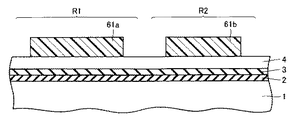
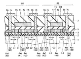
次に、TFTアレイ基板に形成される薄膜トランジスタの構造について説明する。図2に示すように、無アルカリのガラス基板1上に膜厚約50nmのシリコン窒化膜2が形成され、そのシリコン窒化膜2上に膜厚約100nmのシリコン酸化膜3が形成されている。そのシリコン酸化膜3のうち、領域R1に位置するシリコン酸化膜3の部分上にはアイランド状の多結晶シリコン膜が形成されている。
Next, the structure of the thin film transistor formed on the TFT array substrate will be described. As shown in FIG. 2, a
その多結晶シリコン膜には、所定の不純物濃度を有するソース領域45と、そのソース領域45と距離を隔てられた所定の不純物濃度を有するドレイン領域46が形成されている。ソース領域45とドレイン領域46との間に位置する領域には、ソース領域45およびドレイン領域45とそれぞれ距離を隔てられて、所定のチャネル長を有するチャネル領域40が形成されている。
A
ソース領域45とチャネル領域40との間に位置する領域には、GOLD領域41が形成されている。また、ドレイン領域46とチャネル領域40との間に位置する領域には、GOLD領域42が形成されている。GOLD領域41,42のそれぞれの不純物濃度は、チャネル領域40の不純物濃度よりも高く、ソース領域45およびドレイン領域46の不純物濃度よりも低く設定されている。
A
一方、シリコン酸化膜3のうち、領域R2に位置するシリコン酸化膜3の部分上にもアイランド状の多結晶シリコン膜が形成されている。その多結晶シリコン膜においても、領域R1と同様に、所定の不純物濃度を有するチャネル領域40、ソース領域45、ドレイン領域46およびGOLD領域41,42がそれぞれ形成されている。
On the other hand, an island-shaped polycrystalline silicon film is also formed on the
そのアイランド状の多結晶シリコン膜を覆うように、膜厚約100nmのシリコン酸化膜からなるゲート絶縁膜5が形成されている。そのゲート絶縁膜5のうち、領域R1と領域R2に位置するゲート絶縁膜5の部分上にゲート電極6aがそれぞれ形成されている。そのゲート電極6aを覆うように、たとえば膜厚約500nmのシリコン酸化膜からなる層間絶縁膜7が形成されている。
A
その層間絶縁膜7のうち、領域R1に位置する層間絶縁膜7の部分では、ソース領域45の表面を露出するコンタクトホール7aと、ドレイン領域46の表面を露出するコンタクトホール7bがそれぞれ形成されている。そのコンタクトホール7a,7bを充填するように、層間絶縁膜7上にソース電極8aとドレイン電極8bとが形成されている。
Of the
また、領域R2に位置する層間絶縁膜7の部分においても、ソース領域45の表面を露出するコンタクトホール7aと、ドレイン領域46の表面を露出するコンタクトホール7bがそれぞれ形成され、そして、そのコンタクトホール7a,7bを充填するように、層間絶縁膜7上にソース電極8aとドレイン電極8bとが形成されている。
Also in the portion of the
このようにして、領域R1では、ゲート電極6a、ソース領域45、ドレイン領域46、GOLD領域41,42およびチャネル領域40によって薄膜トランジスタT1が構成される。一方、領域R2では、ゲート電極6a、ソース領域45、ドレイン領域46、GOLD領域41,42およびチャネル領域40によって薄膜トランジスタT2が構成される。
Thus, in the region R1, the thin film transistor T1 is configured by the
薄膜トランジスタT1、T2では、それぞれゲート電極6aは、チャネル領域40の全体を覆うように形成されるとともに、GOLD領域41およびGOLD領域42と平面的にオーバラップするように形成されている。
In the thin film transistors T1 and T2, the
つまり、薄膜トランジスタT1では、一方のGOLD領域41とソース領域45との接合部およびゲート電極6aの一方側部とは略同一平面H1上に位置し、他方のGOLD領域42とドレイン領域46との接合部およびゲート電極6aの他方側部は同一平面H2上に位置している。
That is, in the thin film transistor T1, the junction between one
一方、薄膜トランジスタT2では、一方のGOLD領域41とソース領域45との接合部およびゲート電極6aの一方側部とは略同一平面H3上に位置し、他方のGOLD領域42とドレイン領域46との接合部およびゲート電極6aの他方側部は同一平面H4上に位置している。
On the other hand, in the thin film transistor T2, the junction between one
薄膜トランジスタT1,T2では、ソース領域45は不純物として濃度5×10²⁰atom/cm3のリンを含有し、ドレイン領域46も不純物として濃度5×1020atom/cm3のリンを含有する。GOLD領域41,42は、不純物として濃度1×1018atom/cm3のリンを含有する。なお、チャネル領域40は、電気的に活性な不純物を含有しない。
In the thin-film transistor T1, T2, the
また、チャネル領域40の長さ、すなわち、実効ゲート長は3μmとされる。そして、薄膜トランジスタT1のGOLD領域41,42のチャネル長方向の長さ(GOLD長)G1,G2は、ともに1.5μmとされる。一方、薄膜トランジスタT2のGOLD領域41,42のGOLD長G3,G4は、ともに0.5μmとされる。
The length of the
次に、上述した液晶表示装置のTFTアレイ基板の製造方法について説明する。図3に示すように、まず、基板として、コーニング社製1737のガラス基板1の主表面上に、たとえばプラズマCVD(Chemical Vapor Deposition)法により膜厚約50nmのシリコン窒化膜2が形成される。そのシリコン窒化膜2上に、膜厚約100nmのシリコン酸化膜3が形成される。次に、そのシリコン酸化膜3上に膜厚約50nmの非晶質シリコン膜が形成される。
Next, a method for manufacturing the TFT array substrate of the liquid crystal display device described above will be described. As shown in FIG. 3, first, as a substrate, a
なお、シリコン窒化膜2はガラス基板1に含まれる不純物が上方に拡散するのを阻止するために形成される。この不純物の拡散を阻止するための膜としてはシリコン窒化膜の他に、SiON、SiC、AlN、Al2O3などの材料を適用してもよい。また、非晶質シリコン膜の下地膜としてシリコン窒化膜2とシリコン酸化膜3との2層構造としたが、2層構造に限られるものではなく、これらの膜を省いたり、あるいはさらに膜を積層してもよい。
The
次に、非晶質シリコン膜を所定の真空中にて熱処理を施すことにより、非晶質シリコン膜中に存在する不要な水素が除去される。次に、非晶質シリコン膜に、たとえばXeClレーザによるレーザ光を照射することにより、図3に示すように、非晶質シリコン膜が多結晶化されて多結晶シリコン膜4とされる。多結晶シリコン膜4の粒径は約0.5μm程度である。
Next, the amorphous silicon film is subjected to heat treatment in a predetermined vacuum, whereby unnecessary hydrogen existing in the amorphous silicon film is removed. Next, the amorphous silicon film is irradiated with laser light from, for example, a XeCl laser, thereby polycrystallizing the amorphous silicon film into a
次に、その多結晶シリコン膜4の領域R1に位置する部分にはレジストパターン61aが形成され、領域R2に位置する部分にはレジストパターン61bが形成される。次に、そのレジストパターン61a,61bをマスクとして多結晶シリコン膜4に異方性エッチングを施すことにより、図4に示すように、領域R1,R2にアイランド状の多結晶シリコン膜4a,4bがそれぞれ形成される。その後、アッシングと薬液処理を施すことで、レジストパターンが61a,61bが除去される。
Next, a resist
次に、その多結晶シリコン膜4a,4bを覆うように、シリコン酸化膜からなるゲート絶縁膜5が形成される。次に、薄膜トランジスタのしきい値を制御するために、たとえばドーズ量1×10¹²atom/cm2、加速エネルギ60KeVにて多結晶シリコン膜にボロンが注入されて、図5に示すように、アイランド状の不純物領域4aaがそれぞれ形成される。
Next, a
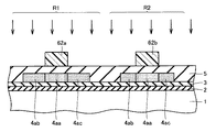
次に、図6に示すように、所定の写真製版処理を施すことにより、領域R1では薄膜トランジスタT1を形成するためのレジストパターン62aが形成されるとともに、領域R2では薄膜トランジスタT2を形成するためのレジストパターン62bが形成される
そのレジストパターン62a,62bをマスクとして、たとえばドーズ量7×10¹²atom/cm2、加速エネルギ80KeVにて不純物領域4aaにリンを注入することにより、領域R1,R2にはそれぞれ不純物領域4ab,4acが形成される。この注入量がGOLD領域における注入量(1×1018atom/cm3)になる。その後、アッシングと薬液処理を施すことで、レジストパターン62a,62bが除去される。
Next, as shown in FIG. 6, by performing a predetermined photoengraving process, a resist
次に、図7に示すように、スパッタ法によりゲート絶縁膜5の全面に膜厚約300nmのクロム膜6が形成される。次に、所定の写真製版処理を施すことにより、領域R1、R2ではそれぞれゲート電極をパターニングするためのレジストパターン63a,63bが形成される。このとき、レジストパターン63aのゲート長方向の長さS1は、レジストパターン63bのゲート長方向の長さS2よりも長く設定される。
Next, as shown in FIG. 7, a
次に、そのレジストパターン63a,63bをマスクとしてクロム膜6にドライエッチングを施すことにより、図8に示すように、領域R1,R2ではそれぞれゲート電極6aが形成される。このとき、領域R1のゲート電極6aの幅(ゲート長方向の長さ)はL1となり、領域R2のゲート電極6aの幅(ゲート長方向の長さ)はL2となる。その後、アッシングと薬液処理を施すことで、レジストパターン63a,63bが除去される。
Next, by performing dry etching on the
なお、このとき、ウエットエッチングによりゲート電極を形成する場合には、ウエットエッチングによってレジストパターンの寸法が短くなる分をあらかじめ含んだ寸法のレジストパターンを形成することが望ましい。 At this time, in the case where the gate electrode is formed by wet etching, it is desirable to form a resist pattern having a dimension that includes a portion in which the dimension of the resist pattern is shortened by wet etching.
次に、ゲート電極6aをマスクとして、たとえばドーズ量3×10¹⁵atom/cm2、加速エネルギ80KeVにてリンを注入することにより、領域R1に位置する不純物領域4ab,4acに、薄膜トランジスタT1のソース領域となる不純物領域4adおよびドレイン領域となる不純物領域4aeがそれぞれ形成される。不純物領域4ad,4aeの不純物濃度は5×1020atom/cm3となる。
Next, using the
一方、領域R2に位置する不純物領域4ab,4acに、薄膜トランジスタT2のソース領域となる不純物領域4adおよびドレイン領域となる不純物領域4aeがそれぞれ形成される。 On the other hand, an impurity region 4ad serving as a source region of the thin film transistor T2 and an impurity region 4ae serving as a drain region are formed in the impurity regions 4ab and 4ac located in the region R2, respectively.
次に、図9に示すように、ゲート電極6aを覆うように、たとえばプラズマCVD法により膜厚約500nmのシリコン酸化膜からなる層間絶縁膜7が形成される。次に、その層間絶縁膜7上に所定の写真製版処理を施すことにより、コンタクトホールを形成するためのレジストパターン(図示せず)が形成される。そのレジストパターンをマスクとして、層間絶縁膜7およびゲート絶縁膜5に異方性エッチングを施すことにより、領域R1,R2のそれぞれにおいて、不純物領域4adの表面を露出するコンタクトホール7aと、不純物領域4aeの表面を露出するコンタクトホール7bが形成される。
Next, as shown in FIG. 9, an
次に、コンタクトホール7a,7bを充填するように、層間絶縁膜7上にクロム膜とアルミニウム膜との積層膜(図示せず)が形成される。その積層膜上に所定の写真製版処理を施すことにより、電極を形成するためのレジストパターン(図示せず)が形成される。次に、そのレジストパターンをマスクとしてウエットエッチングを施すことにより、ソース電極8aとドレイン電極8bが形成される。
Next, a laminated film (not shown) of a chromium film and an aluminum film is formed on the
以上の工程を経て、図2に示される薄膜トランジスタT1,T2を備えたTFTアレイ基板の主要部分が形成される。薄膜トランジスタT1,T2では、不純物領域4adがソース領域45となり、不純物領域4aeがドレイン領域46となり、不純物領域4ab,4acがGOLD領域41,42となり、不純物領域4aaがチャネル領域40となる。
Through the above steps, the main part of the TFT array substrate including the thin film transistors T1 and T2 shown in FIG. 2 is formed. In the thin film transistors T1 and T2, the impurity region 4ad becomes the
上述したTFTアレイ基板では、1枚のガラス基板1上にGOLD長の異なる薄膜トランジスタが形成されることで、回路に要求される特性に応じて最適なGOLD長を有する薄膜トランジスタを適用することができる。そして、GOLD長の異なる薄膜トランジスタを形成することによって、薄膜トランジスタの占有面積を削減することができる。以下、このことについて詳しく説明する。
In the TFT array substrate described above, thin film transistors having different GOLD lengths are formed on one
液晶表示装置に使用されるTFTアレイ基板では、一定のコントラストを確保して液晶を駆動するための所定の電圧を確保するために、回路の駆動電圧を一律に下げることができない。 In a TFT array substrate used in a liquid crystal display device, the driving voltage of a circuit cannot be reduced uniformly in order to secure a predetermined voltage for driving a liquid crystal while ensuring a certain contrast.
これに対して、液晶の膜厚を薄くすれば、駆動電圧を下げることはできる。しかしながら、液晶の厚さが薄くなるとバックライトの光を十分に遮光することができなくなる。そのため、黒の表示を鮮明に行なうことができなくなって、コントラストが低下することになる。したがって、液晶表示装置では、液晶を駆動するための電圧を5V以下に設定することができない。 On the other hand, if the film thickness of the liquid crystal is reduced, the drive voltage can be lowered. However, if the thickness of the liquid crystal is reduced, the light from the backlight cannot be sufficiently blocked. Therefore, it becomes impossible to display black clearly and the contrast is lowered. Therefore, in the liquid crystal display device, the voltage for driving the liquid crystal cannot be set to 5 V or less.
液晶を駆動するための電圧として5Vを確保するために、画素部21の画素薄膜トランジスタ22、その画素部薄膜トランジスタ22に電源電圧を供給するための電源回路33、対向電極駆動回路32、階調電圧回路34、画素部薄膜トランジスタ22に画素データを転送するソースドライバ30に使用される薄膜トランジスタの駆動電圧はそれぞれ5Vとされる。その他の回路における薄膜トランジスタの駆動電圧は3.3Vとされる。
In order to secure 5 V as a voltage for driving the liquid crystal, the pixel
駆動電圧として異なる2つの電圧が使用されることで、薄膜トランジスタのソース・ドレイン耐圧も、駆動電圧に対応した耐圧を有していることが望ましい。 It is desirable that the source / drain withstand voltage of the thin film transistor has a withstand voltage corresponding to the drive voltage by using two different voltages as the drive voltage.
ここで、薄膜トランジスタにおけるGOLD長とソース・ドレイン耐圧との関係を図10に示す。図10に示すように、GOLD長が長くなるにしたがってソース・ドレイン耐圧は増大し、GOLD長が2μmを超えるとソース・ドレイン耐圧はほとんど向上せず飽和する傾向にある。GOLD長が0.5μmの場合の薄膜トランジスタのソース・ドレイン耐圧は約13Vであり、GOLD長が1.5μmの薄膜トランジスタのソース・ドレイン耐圧は18Vであることがわかる。 Here, FIG. 10 shows the relationship between the GOLD length and the source / drain breakdown voltage in the thin film transistor. As shown in FIG. 10, the source / drain withstand voltage increases as the GOLD length increases, and when the GOLD length exceeds 2 μm, the source / drain withstand voltage hardly increases and tends to be saturated. It can be seen that when the GOLD length is 0.5 μm, the source / drain withstand voltage of the thin film transistor is about 13V, and the thin film transistor with the GOLD length of 1.5 μm has a source / drain withstand voltage of 18V.
本実施の形態に係る液晶表示装置のTFT基板では、信号制御回路27など電圧3.3Vのもとで使用される回路の薄膜トランジスタとして、GOLD長が0.5μmの薄膜トランジスタが適用される。一方、液晶を駆動するための回路など電圧5Vのもとで使用される回路の薄膜トランジスタとして、GOLD長が1.5μmの薄膜トランジスタが適用される。なお、信頼性の観点からソース・ドレイン耐圧は使用電圧の3倍以上になるように設定することが望ましい。
In the TFT substrate of the liquid crystal display device according to the present embodiment, a thin film transistor having a GOLD length of 0.5 μm is applied as a thin film transistor of a circuit used under a voltage of 3.3 V such as the
このように、上述したTFTアレイ基板では、電圧が高い回路には、薄膜トランジスタとして、比較的GOLD長の長い薄膜トランジスタが適用される一方、電圧が低い回路には、薄膜トランジスタとして、比較的GOLD長の短い薄膜トランジスタが適用される。 Thus, in the TFT array substrate described above, a thin film transistor having a relatively long GOLD length is applied to a circuit having a high voltage as a thin film transistor, whereas a thin film transistor having a relatively short GOLD length is applied to a circuit having a low voltage. Thin film transistors are applied.
液晶表示装置に使用される薄膜トランジスタにおいては、上記のように駆動電圧が下げられないために、通常のLSI(Large Scale Integrated Circuit)に使用されるトランジスタと比べると、比較的長いGOLD長、たとえば1.5μm程度のGOLD長を設定する必要がある。通常のLSIに使用される薄膜トランジスタのGOLD長は0.1μm程度である。 In the thin film transistor used in the liquid crystal display device, since the driving voltage cannot be lowered as described above, the GOLD length, for example, 1 is relatively long compared to a transistor used in a normal LSI (Large Scale Integrated Circuit). It is necessary to set a GOLD length of about 5 μm. A GOLD length of a thin film transistor used in a normal LSI is about 0.1 μm.
薄膜トランジスタのGOLD長によって、薄膜トランジスタの占有面積は大きく変動する。たとえば、GOLD長0.5μm、ゲート幅10μm、実効ゲート長3μmの薄膜トランジスタ1つあたりの占有面積は、ソース電極およびドレイン電極を除くと、約160μm2となる。これに対して、GOLD長が1.5μmの薄膜トランジスタ1つの占有面積は、約180μm2となる。 The occupied area of the thin film transistor varies greatly depending on the GOLD length of the thin film transistor. For example, the occupied area per thin film transistor having a GOLD length of 0.5 μm, a gate width of 10 μm, and an effective gate length of 3 μm is about 160 μm 2 excluding the source electrode and the drain electrode. On the other hand, the occupied area of one thin film transistor having a GOLD length of 1.5 μm is about 180 μm 2 .
このことから、TFTアレイ基板におけるすべての薄膜トランジスタのGOLD長を1.5μmに設定したとすれば、TFTアレイ基板において薄膜トランジスタの占有面積は非常に大きくなってしまう。 Therefore, if the GOLD length of all the thin film transistors in the TFT array substrate is set to 1.5 μm, the area occupied by the thin film transistors in the TFT array substrate becomes very large.
上述した液晶表示装置のTFTアレイ基板では、GOLD長0.5μmの薄膜トランジスタと、GOLD長1.5μmの薄膜トランジスタを適用することによって、GOLD長0.5μmの薄膜トランジスタ1つあたりについて、GOLD長1.5μmの薄膜トランジスタ1つの占有面積よりも約20μm2削減できることになる。これは、GOLD長1.5μmの薄膜トランジスタ1つの占有面積の約11%に相当する。 In the TFT array substrate of the liquid crystal display device described above, by applying a thin film transistor having a GOLD length of 0.5 μm and a thin film transistor having a GOLD length of 1.5 μm, a GOLD length of 1.5 μm is obtained for each thin film transistor having a GOLD length of 0.5 μm. Thus, the area occupied by one thin film transistor can be reduced by about 20 μm 2 . This corresponds to about 11% of the occupied area of one thin film transistor having a GOLD length of 1.5 μm.
そうすると、TFTアレイ基板に形成される薄膜トランジスタの全体では、GOLD長0.5μmの薄膜トランジスタの数を約10000とすると、約0.2mm2(20μm2×10000)程度の薄膜トランジスタの占有面積を削減することができることになる。 Then, the total area of the thin film transistors formed on the TFT array substrate is about 0.2 mm 2 (20 μm 2 × 10000) when the number of thin film transistors having a GOLD length of 0.5 μm is about 10,000. Will be able to.
また、上述した液晶表示装置のTFTアレイ基板では、電圧が低い回路に対して比較的GOLD長の短い薄膜トランジスタを適用することによって、以下に述べるように、薄膜トランジスタの寄生容量が減少して、動作速度をより速くする効果も得られる。 Further, in the TFT array substrate of the liquid crystal display device described above, by applying a thin film transistor having a relatively short GOLD length to a circuit having a low voltage, as described below, the parasitic capacitance of the thin film transistor is reduced and the operation speed is reduced. The effect of making it faster can also be obtained.
GOLD長0.5μmの薄膜トランジスタの占有面積とGOLD長1.5μmの薄膜トランジスタの占有面積との差20μm2は、GOLD領域の面積である。図2に示すように、そのGOLD領域41,42は多結晶シリコン膜に形成され、GOLD領域41,42とゲート電極6aとは薄いゲート絶縁膜5を介在させて対向している。そのため、GOLD領域の面積が大きいほどGOLD領域とゲート電極との間の寄生容量も大きくなる。したがって、GOLD領域の面積を削減することによって、GOLD領域とゲート電極との間の寄生容量が低減して、回路の動作速度を向上することができることになる。
The difference of 20 μm 2 between the occupied area of the thin film transistor having a GOLD length of 0.5 μm and the occupied area of the thin film transistor having a GOLD length of 1.5 μm is the area of the GOLD region. As shown in FIG. 2, the
なお、上述した液晶表示装置では、薄膜トランジスタT1のGOLD領域41,42の不純物濃度として1×10¹⁸atom/cm3の場合を例に挙げて説明したが、GOLD領域41,42の不純物濃度としてはこの濃度に限られるものではない。チャネル領域40の不純物濃度より高く、ソース領域45およびドレイン領域46の不純物濃度より低ければソース・ドレイン耐圧を向上することができる。
In the liquid crystal display device described above, the case where the impurity concentration of the
また、ソース・ドレイン耐圧を十分に確保するには、GOLD領域41,42の不純物濃度は1×10¹⁷atom/cm3以上で1×1019atom/cm3以下であることが望ましい。
In order to sufficiently secure the source / drain breakdown voltage, it is desirable that the impurity concentration of the
なお、上述した液晶表示装置では、使用される電圧として3.3Vと5Vの2系統の場合を例に挙げて説明したが、液晶表示装置としては、3.3Vよりもさらに低い電圧によって動作する回路を備えている場合も想定される。そのような液晶表示装置のTFTアレイ基板では、さらに、GOLD領域を備えない薄膜トランジスタを形成してもよい。 In the liquid crystal display device described above, the case where two voltages of 3.3V and 5V are used has been described as an example, but the liquid crystal display device operates with a voltage lower than 3.3V. A case where a circuit is provided is also assumed. In such a TFT array substrate of a liquid crystal display device, a thin film transistor that does not have a GOLD region may be formed.
すなわち、図11に示すように、領域R1および領域R2にはそれぞれGOLD領域を備えた薄膜トランジスタT1,T2が形成されるとともに、領域R3にはGOLD領域を備えない薄膜トランジスタT3が形成される。3.3Vよりもさらに低い電圧によって動作する回路には、薄膜トランジスタT3が適用される。薄膜トランジスタT3は、ゲート電極6a、ソース領域45、ドレイン領域46およびチャネル領域40によって構成される。
That is, as shown in FIG. 11, thin film transistors T1 and T2 each having a GOLD region are formed in the region R1 and the region R2, and a thin film transistor T3 not having a GOLD region is formed in the region R3. The thin film transistor T3 is applied to a circuit that operates with a voltage lower than 3.3V. The thin film transistor T3 includes a
この液晶表示装置では、3.3Vよりもさらに低い電圧によって動作する回路に対してGOLD領域を備えた薄膜トランジスタを適用する場合と比べると、そのような回路にGOLD領域を備えない薄膜トランジスタT3を適用することによって、薄膜トランジスタの占有面積をさらに低減するが可能になる。なお、薄膜トランジスタとしてnチャネル型の薄膜トランジスタを例に挙げたが、pチャネル型の薄膜トランジスタにも適用することができる。 In this liquid crystal display device, the thin film transistor T3 not having the GOLD region is applied to such a circuit as compared with the case where the thin film transistor having the GOLD region is applied to a circuit operating at a voltage lower than 3.3V. As a result, the area occupied by the thin film transistor can be further reduced. Note that although an n-channel thin film transistor is described as an example as a thin film transistor, the present invention can also be applied to a p-channel thin film transistor.
実施の形態2
ここでは、GOLD領域に加えてLDD領域を含む薄膜トランジスタを有する液晶表示装置のTFTアレイ基板を例に挙げる。
Here, a TFT array substrate of a liquid crystal display device having a thin film transistor including an LDD region in addition to the GOLD region is taken as an example.
図12に示すように、領域R1に位置する多結晶シリコン膜には、所定の不純物濃度を有するソース領域45と、そのソース領域45と距離を隔てられた所定の不純物濃度を有するドレイン領域46が形成されている。ソース領域45とドレイン領域46との間に位置する領域には、ソース領域45およびドレイン領域45とそれぞれ距離を隔てられて、所定のチャネル長を有するチャネル領域40が形成されている。
As shown in FIG. 12, a
ソース領域45とチャネル領域40との間に位置する領域には、ソース領域45の側にLDD領域43が形成され、チャネル領域40の側にGOLD領域41が形成されている。また、ドレイン領域46とチャネル領域40との間に位置する領域には、ドレイン領域46の側にLDD領域44が形成され、チャネル領域40の側にGOLD領域42が形成されている。
In a region located between the
領域R1では、これらチャネル領域40、ソース領域45、ドレイン領域46、GOLD領域41,42およびLDD領域43,44と、ゲート電極6aとによって薄膜トランジスタT4が構成される。
In the region R1, the
一方、領域R2に位置する多結晶シリコン膜にも、領域R1と同様に、所定の不純物濃度を有するチャネル領域40、ソース領域45、ドレイン領域46、GOLD領域41,42およびLDD領域43,44がそれぞれ形成されている。領域R2では、これらチャネル領域40、ソース領域45、ドレイン領域46、GOLD領域41,42およびLDD領域43,44と、ゲート電極6aとによって薄膜トランジスタT5が構成される。
On the other hand, similarly to the region R1, the polycrystalline silicon film located in the region R2 has a
なお、これ以外の構成については、図2に示す構造と同様なので、同一部材には同一符号を付しその説明を省略する。 In addition, since it is the same as that of the structure shown in FIG. 2 about another structure, the same code | symbol is attached | subjected to the same member and the description is abbreviate | omitted.
薄膜トランジスタT4、T5では、それぞれゲート電極6aは、チャネル領域40の全体を覆うように形成されるとともに、GOLD領域41およびGOLD領域42と平面的にオーバラップするように形成されている。
In the thin film transistors T4 and T5, the
つまり、薄膜トランジスタT4では、一方のGOLD領域41とLDD領域43との接合部およびゲート電極6aの一方側部とは略同一平面H5上に位置し、他方のGOLD領域42とLDD領域44との接合部およびゲート電極6aの他方側部は同一平面H6上に位置している。
That is, in the thin film transistor T4, the junction between one
一方、薄膜トランジスタT5では、一方のGOLD領域41とLDD領域43との接合部およびゲート電極6aの一方側部とは略同一平面H7上に位置し、他方のGOLD領域42とLDD領域44との接合部およびゲート電極6aの他方側部は同一平面H8上に位置している。
On the other hand, in the thin film transistor T5, the junction between one
薄膜トランジスタT4,T5では、ソース領域45は不純物として濃度5×10²⁰atom/cm3のリンを含有し、ドレイン領域46も不純物として濃度5×1020atom/cm3のリンを含有する。GOLD領域41,42は、不純物として濃度1×1018atom/cm3のリンを含有する。LDD領域43,44は、不純物として濃度5×1018atom/cm3のリンを含有する。チャネル領域40は、電気的に活性な不純物を含有しない。
In the thin film transistor T4, T5,
薄膜トランジスタT4のGOLD領域41,42のGOLD長G1,G2は、ともに2.0μmとされる。一方、薄膜トランジスタT5のGOLD領域41,42のGOLD長G3,G4は、ともに0.5μmとされる。また、薄膜トランジスタT4のLDD領域43,44のチャネル長方向の長さ(LDD長)L1,L2と、薄膜トランジスタT5のLDD領域43,44のLDD長L3,L4は、いずれも0.5μmとされる。
The GOLD lengths G1 and G2 of the
次に、上述した液晶表示装置のTFTアレイ基板の製造方法について説明する。まず実施の形態1において説明した図1〜図5に示す工程を経た後、図6に示す工程と同様にして、図13に示すように、所定の写真製版処理を施すことにより、領域R1では薄膜トランジスタT4を形成するためのレジストパターン62aが形成されるとともに、領域R2では薄膜トランジスタT5を形成するためのレジストパターン62bが形成される
そのレジストパターン62a,62bをマスクとして、たとえばドーズ量7×10¹²atom/cm2、加速エネルギ80KeVにて不純物領域4aaにリンを注入することにより、領域R1,R2にはそれぞれ不純物領域4ab,4acが形成される。この注入量がGOLD領域における注入量(1×1018atom/cm3)になる。その後、アッシングと薬液処理を施すことで、レジストパターン62a,62bが除去される。
Next, a method for manufacturing the TFT array substrate of the liquid crystal display device described above will be described. First, after the steps shown in FIGS. 1 to 5 described in the first embodiment, in the same manner as the step shown in FIG. 6, a predetermined photoengraving process is performed in the region R1 as shown in FIG. A resist
次に、図7に示す工程と同様の工程を経て、領域R1、R2ではそれぞれゲート電極をパターニングするためのレジストパターン63a,63b(図14参照)が形成される。そのレジストパターン63a,63bをマスクとしてクロム膜にウエットエッチングを施すことにより、図14に示すように、領域R1,R2ではそれぞれゲート電極6aが形成される。なお、ウェットエッチングを施す際に露出するクロム膜の側面にサイドエッチングが施されることになるが、そのエッチングされる量はオーバーエッチングを施す時間によって制御することができる。
Next, through steps similar to those shown in FIG. 7, resist
次に、レジストパターン63a,63bをマスクとして、たとえばドーズ量8×10¹⁴atom/cm2、加速エネルギ80KeVにて不純物領域4ab,4acにリンを注入することにより、ソース領域およびドレイン領域となる不純物領域4ad,4aeが形成される。不純物領域4ad,4aeの不純物濃度は、5×1020atom/cm3となる。その後、アッシングと薬液処理を施すことで、レジストパターンが63a,63bが除去される。
Next, using resist
次に、図15に示すように、ゲート電極6aをマスクとして、たとえばドーズ量3×10¹³atom/cm2、加速エネルギ80KeVにてリンを注入することにより残された不純物領域4ab,4acにLDD領域となる不純物領域4af,4agがそれぞれ形成される。LDD領域となる不純物領域4af,4agの不純物濃度(5×1018atom/cm3)は、当該リンの注入量と、GOLD領域を形成するためのリンの注入量とによって決まることになる。
Next, as shown in FIG. 15, by using the
このようして、LDD領域となる不純物領域4af,4agが形成されることで、LDD領域となる不純物領域4af,4agの不純物濃度は、GOLD領域となる不純物領域4ab,4acの不純物濃度よりも高くなる。 Thus, by forming the impurity regions 4af and 4ag serving as the LDD regions, the impurity concentration of the impurity regions 4af and 4ag serving as the LDD regions is higher than the impurity concentration of the impurity regions 4ab and 4ac serving as the GOLD regions. Become.
その後、図9に示す工程と同様の工程を経て、図12に示される薄膜トランジスタT4,T5を備えたTFTアレイ基板の主要部が形成される。 Thereafter, the main part of the TFT array substrate including the thin film transistors T4 and T5 shown in FIG. 12 is formed through the same process as that shown in FIG.
上述したTFTアレイ基板では、1枚のガラス基板1上にGOLD長の異なる薄膜トランジスタT4,T5が形成されることで、回路に要求される特性に応じて最適な薄膜トランジスタT4,T5を適用することができることに加えて、薄膜トランジスタT4,T5がLDD領域を備えていることによって、薄膜トランジスタT4,T5のソース・ドレイン耐圧をさらに向上することができる。
In the above-described TFT array substrate, thin film transistors T4 and T5 having different GOLD lengths are formed on one
薄膜トランジスタT4,T5のソース・ドレイン耐圧がさらに向上することによって、より高い電圧(回路電圧)に対応することができる。すなわち、動画表示などの動作速度を速めるためのTFTアレイ基板、あるいは、解像度を増大させた大画面等のためのTFTアレイ基板として、このTFTアレイ基板を適用することができる。 By further improving the source / drain withstand voltage of the thin film transistors T4 and T5, it is possible to cope with a higher voltage (circuit voltage). That is, this TFT array substrate can be applied as a TFT array substrate for increasing the operation speed of moving image display or the like, or as a TFT array substrate for a large screen with increased resolution.
特に、解像度が増加すると、ソースドライバ30の動作周波数(データ線26の周波数)は高くなる。たとえば、解像度VGA(Video Graphics Array)の場合の画素数は640×480であり、その駆動に必要なデータ線の動作周波数は25MHzであるのに対して、解像度XGA(eXtended Graphics Array)の場合の画素数は1024×768であり、その駆動に必要なデータ線の動作周波数は65MHzにまで高くなる。このように大画面のTFTアレイ基板を動作させるためには、電源電圧を上げて動作速度を速くしなければならない。 In particular, when the resolution increases, the operating frequency of the source driver 30 (the frequency of the data line 26) increases. For example, in the case of resolution VGA (Video Graphics Array), the number of pixels is 640 × 480, and the operating frequency of the data line necessary for driving is 25 MHz, whereas in the case of resolution XGA (eXtended Graphics Array) The number of pixels is 1024 × 768, and the operating frequency of the data line necessary for driving the pixel line is as high as 65 MHz. In order to operate the TFT array substrate having a large screen as described above, the operation speed must be increased by increasing the power supply voltage.
本実施の形態に係る液晶表示装置のTFTアレイ基板では、高速動作を図るためにソースドライバ30(図1参照)の駆動電圧は7Vに昇圧されている。そのソースドライバ30の回路など電圧7Vのもとで使用される回路の薄膜トランジスタとして、GOLD長が2.0μmの薄膜トランジスタが適用される。一方、信号制御回路35など電圧3.3Vのもとで使用される回路の薄膜トランジスタとして、GOLD長が0.5μmの薄膜トランジスタが適用される。
In the TFT array substrate of the liquid crystal display device according to the present embodiment, the drive voltage of the source driver 30 (see FIG. 1) is boosted to 7 V in order to achieve high-speed operation. A thin film transistor having a GOLD length of 2.0 μm is applied as a thin film transistor of a circuit used under a voltage of 7 V, such as the circuit of the
上述した液晶表示装置のTFTアレイ基板では、薄膜トランジスタにGOLD領域に加えてLDD領域が形成されていることで、ソース・ドレイン耐圧をさらに向上することができる。 In the TFT array substrate of the liquid crystal display device described above, the source / drain breakdown voltage can be further improved by forming the LDD region in addition to the GOLD region in the thin film transistor.
また、電圧が高い回路には、比較的GOLD長の長い薄膜トランジスタが適用される一方、電圧が低い回路には、比較的GOLD長の短い薄膜トランジスタが適用されることで、前述したように、薄膜トランジスタの占有面積を削減することができる。 In addition, a thin film transistor with a relatively long GOLD length is applied to a circuit with a high voltage, whereas a thin film transistor with a relatively short GOLD length is applied to a circuit with a low voltage, so that Occupied area can be reduced.
実施の形態3
ここでは、液晶表示装置のTFTアレイ基板のバリエーションの一例として、実施の形態1において説明した薄膜トランジスタT1,T2と、実施の形態2において説明した薄膜トランジスタT4,T5とを有するTFTアレイ基板について説明する。
Here, as an example of a variation of the TFT array substrate of the liquid crystal display device, a TFT array substrate having the thin film transistors T1 and T2 described in the first embodiment and the thin film transistors T4 and T5 described in the second embodiment will be described.
図16に示すように、TFTアレイ基板において、領域R1および領域R2には、GOLD領域とLDD領域の双方を備えた薄膜トランジスタT4,T5がそれぞれ形成されている。一方、領域R3および領域R4には、LDD領域を備えずにGOLD領域だけを備えた薄膜トランジスタT1,T2がそれぞれ形成されている。基本的な構造は、図2および図12にそれぞれ示される構造と同様なので、同一部材には同一符号を付しその説明を省略する。 As shown in FIG. 16, in the TFT array substrate, thin film transistors T4 and T5 having both a GOLD region and an LDD region are formed in the region R1 and the region R2, respectively. On the other hand, in the region R3 and the region R4, thin film transistors T1 and T2 each including only the GOLD region without forming the LDD region are formed. Since the basic structure is the same as the structure shown in FIGS. 2 and 12, the same reference numerals are given to the same members, and the description thereof is omitted.
薄膜トランジスタT1では、GOLD領域41,42のGOLD長G1,G2は、ともに1.5μmとされる。薄膜トランジスタT2では、GOLD領域41,42のGOLD長G3,G4は、ともに0.5μmとされる。
In the thin film transistor T1, the GOLD lengths G1 and G2 of the
薄膜トランジスタT4では、GOLD領域41,42のGOLD長G1,G2は、ともに2.0μmとされ、LDD領域43,44のチャネル長方向の長さ(LDD長)L1,L2は、ともに0.5μmとされる。薄膜トランジスタT5では、GOLD領域41,42のGOLD長G3,G4は、ともに0.5μmとされ、LDD領域43,44のLDD長L3,L4は、ともに0.5μmとされる。
In the thin film transistor T4, the GOLD lengths G1 and G2 of the
したがって、TFTアレイ基板には、ソース・ドレイン耐圧のそれぞれ異なる4種類の薄膜トランジスタT1,T2,T4,T5がガラス基板1上に形成されていることになり、液晶表示装置としては、互いに異なる4系統の電圧を使用することが可能になる。
Therefore, four types of thin film transistors T1, T2, T4, and T5 having different source / drain withstand voltages are formed on the
液晶表示装置として、液晶の応答速度を速くしようとして、液晶(画素容量23)の駆動電圧を5Vからたとえば6Vへ昇圧したとすると、電圧としては、7V,6V,5V,3.3Vの4つの電圧が使用されることになる。 As a liquid crystal display device, if the drive voltage of the liquid crystal (pixel capacitor 23) is boosted from 5V to, for example, 6V in order to increase the response speed of the liquid crystal, there are four voltages of 7V, 6V, 5V, and 3.3V. Voltage will be used.
本実施の形態に係る液晶表示装置のTFTアレイ基板では、ソースドライバ30の回路など電圧7Vのもとで使用される回路の薄膜トランジスタとして、薄膜トランジスタT4が適用される。階調電圧回路34および対向電極駆動回路32など電圧6Vのもとで使用される回路の薄膜トランジスタとして、薄膜トランジスタT5が適用される。
In the TFT array substrate of the liquid crystal display device according to the present embodiment, the thin film transistor T4 is applied as a thin film transistor of a circuit used under a voltage of 7 V, such as a circuit of the
ゲートドライバ31および電源回路33など電圧5Vのもとで使用される回路の薄膜トランジスタとして、薄膜トランジスタT1が適用される。信号制御回路35など電圧3.3Vのもとで使用される回路の薄膜トランジスタとして、薄膜トランジスタT2が適用される。
A thin film transistor T1 is applied as a thin film transistor of a circuit used under a voltage of 5 V, such as the
上述した液晶表示装置のTFTアレイ基板では、TFTアレイ基板におけるすべての薄膜トランジスタのGOLD長を最も高い電圧に対応したGOLD長に設定した場合と比べると、電圧に応じたGOLD長を有する薄膜トランジスタを適用することによって、薄膜トランジスタの占有面積を削減することができる。 In the TFT array substrate of the liquid crystal display device described above, a thin film transistor having a GOLD length corresponding to the voltage is applied as compared to the case where the GOLD length of all the thin film transistors in the TFT array substrate is set to the GOLD length corresponding to the highest voltage. As a result, the area occupied by the thin film transistor can be reduced.
そして、GOLD領域に加えてLDD領域が形成された薄膜トランジスタT4,T5を備えていることで、ソース・ドレイン耐圧が向上して、より高い電圧に対応することができて、液晶表示装置の動作速度の向上を図ることができる。 The thin film transistors T4 and T5 in which the LDD region is formed in addition to the GOLD region can improve the source / drain breakdown voltage and can cope with a higher voltage, and the operation speed of the liquid crystal display device. Can be improved.
LDD領域を備えずにGOLD領域だけを備えた薄膜トランジスタT1,T2と、GOLD領域とLDD領域の双方を備えた薄膜トランジスタT4,T5とを同一基板上に形成するには、まず、図13に示す工程において、領域R1,R2,R3,R4にそれぞれ形成される薄膜トランジスタT1,T2,T4,T5のGOLD領域を形成する。次に、図14に示す工程では、領域R3,R4をレジストパターンで覆い、薄膜トランジスタT1,T2のゲート電極を形成させないようにする。その後、他のマスク(レジストパターン)を用いて、領域R3,R4の薄膜トランジスタT1,T2を形成すればよい。具体的な製造方法は、実施の形態1、2において説明した方法を適用することができる。
In order to form the thin film transistors T1 and T2 having only the GOLD region without the LDD region and the thin film transistors T4 and T5 having both the GOLD region and the LDD region on the same substrate, first, a process shown in FIG. , The GOLD regions of the thin film transistors T1, T2, T4, and T5 formed in the regions R1, R2, R3, and R4, respectively, are formed. Next, in the step shown in FIG. 14, the regions R3 and R4 are covered with a resist pattern so that the gate electrodes of the thin film transistors T1 and T2 are not formed. Thereafter, the thin film transistors T1 and T2 in the regions R3 and R4 may be formed using another mask (resist pattern). As a specific manufacturing method, the method described in
なお、上述した各実施の形態における液晶表示装置のTFTアレイ基板では、GOLD領域を備えた薄膜トランジスタとしてnチャネル型の薄膜トランジスタを例に挙げたが、それは次の理由による。n型トランジスタのキャリアは電子であり、p型トランジスタのキャリアは正孔である。半導体中ではキャリアの有効質量は電子の方が正孔よりも軽いことで、nチャネル型の薄膜トランジスタの方がアバランシェ崩壊を起こしやすいために、ソース・ドレイン耐圧が低くなる。そのため、nチャネル型の薄膜トランジスタでは、GOLD領域を備えていることが望ましい。 In the TFT array substrate of the liquid crystal display device in each of the above-described embodiments, an n-channel thin film transistor is given as an example of a thin film transistor provided with a GOLD region, for the following reason. The carrier of the n-type transistor is an electron, and the carrier of the p-type transistor is a hole. In semiconductors, the effective mass of carriers is that electrons are lighter than holes, and an n-channel thin film transistor is more prone to avalanche collapse, resulting in a lower source / drain breakdown voltage. Therefore, an n-channel thin film transistor desirably includes a GOLD region.
また、電子の有効質量が小さく、そして、電子のシリコン酸化膜への障壁高さ(シリコンの伝導帯とシリコン酸化膜の伝導帯のエネルギー差=3.1eV)が、正孔のシリコン酸化膜への障壁高さ(シリコンの価電子帯とシリコン酸化膜の価電子帯のエネルギー差=3.8eV)よりも小さいことで、電子の方がゲート絶縁膜(シリコン酸化膜)に注入されて、ゲート絶縁膜がダメージを受けやすく、nチャネル型の薄膜トランジスタの方が素子としての特性が劣化して信頼性が損なわれやすい。そのため、信頼性を確保する観点からも、nチャネル型の薄膜トランジスタにはGOLD領域を備えていることが望ましい。 Also, the effective mass of electrons is small, and the barrier height of electrons to the silicon oxide film (energy difference between the conduction band of silicon and the conduction band of silicon oxide = 3.1 eV) is reduced to the silicon oxide film of holes. Is smaller than the barrier height (energy difference between the valence band of silicon and the valence band of silicon oxide film = 3.8 eV), so that electrons are injected into the gate insulating film (silicon oxide film) and The insulating film is easily damaged, and the characteristics of the n-channel thin film transistor are more deteriorated and the reliability is more easily lost. Therefore, from the viewpoint of ensuring reliability, it is desirable that the n-channel thin film transistor includes a GOLD region.
なお、GOLD領域を備えた薄膜トランジスタとしてはnチャネル型の薄膜トランジスタに限られるものではなく、pチャネル型の薄膜トランジスタであってもよい。 Note that the thin film transistor including the GOLD region is not limited to an n-channel thin film transistor, and may be a p-channel thin film transistor.
また、上述した液晶表示装置におけるTFTアレイ基板では、GOLD領域を備えた薄膜トランジスタのGOLD長として、3種類(0.5μm、1.5μm、2.0μm)の場合を例に挙げて説明したが、GOLD長としてはこれらに限られるものではなく、使用される電圧に応じたGOLD長を適用することができる。そのようなGOLD長としては、0.1μm以上2.0μm以下であることが望ましい。 In the TFT array substrate in the liquid crystal display device described above, the GOLD length of the thin film transistor provided with the GOLD region has been described as an example of three types (0.5 μm, 1.5 μm, and 2.0 μm). The GOLD length is not limited to these, and a GOLD length corresponding to the voltage used can be applied. Such GOLD length is preferably 0.1 μm or more and 2.0 μm or less.
ここで、上限値を2.0μmとするのは、上述したように、GOLD長が2μmを超えてもソース・ドレイン耐圧はほとんど向上せず、薄膜トランジスタの占有面積が増加するためである。一方、下限値を0.1μmとするのは次の理由による。 Here, the reason why the upper limit value is set to 2.0 μm is that, as described above, even if the GOLD length exceeds 2 μm, the source / drain breakdown voltage is hardly improved and the area occupied by the thin film transistor is increased. On the other hand, the lower limit is set to 0.1 μm for the following reason.
薄膜トランジスタを適用した画像表示装置において、設計の自由度を上げるために薄膜トランジスタにすべての信号を処理させる場合も想定される。すべての信号をTFTアレイ基板にて行なうとするとTFTアレイ基板に組み込まれる回路が増大するため、基板面積の増大を最小限に抑えるために薄膜トランジスタの微細化が必要とされる。このとき、その微細化された薄膜トランジスタをたとえば電源電圧1.8Vあるいは1.3V程度の比較的低い電圧で動作させるとすると、GOLD長が0.1μm以上であればソース・ドレイン耐圧を十分に確保することができる。すなわち、GOLD長が0.1μm以上であれば、薄膜トランジスタの微細化を図って、かつ、ソース・ドレイン耐圧を確保することができる。 In an image display device to which a thin film transistor is applied, it is assumed that all signals are processed by the thin film transistor in order to increase the degree of design freedom. If all signals are performed on the TFT array substrate, the number of circuits incorporated in the TFT array substrate increases. Therefore, miniaturization of the thin film transistor is required to minimize the increase in the substrate area. At this time, if the miniaturized thin film transistor is operated at a relatively low voltage of about 1.8 V or 1.3 V, for example, the source / drain breakdown voltage is sufficiently secured if the GOLD length is 0.1 μm or more. can do. That is, if the GOLD length is 0.1 μm or more, the thin film transistor can be miniaturized and the source / drain breakdown voltage can be secured.
また、上述した各実施の形態においては、薄膜トランジスタとしてソース領域およびドレイン領域等が形成される多結晶シリコン膜上にゲート絶縁膜を介在させてゲート電極が形成された、いわゆるプレーナ構造の薄膜トランジスタを例に挙げて説明した。 Further, in each of the above-described embodiments, a thin film transistor having a so-called planar structure in which a gate electrode is formed on a polycrystalline silicon film in which a source region, a drain region, and the like are formed as a thin film transistor with a gate insulating film interposed. And explained.
本発明に係る液晶表示装置の薄膜トランジスタとしては、このようなプレーナ構造の薄膜トランジスタに限られず、ゲート電極上にゲート絶縁膜を介在させてソース領域およびドレイン領域等となる半導体層を形成した、いわゆる逆スタガ構造の薄膜トランジスタであってもよい。 The thin film transistor of the liquid crystal display device according to the present invention is not limited to such a thin film transistor having a planar structure, but a so-called reverse structure in which a semiconductor layer serving as a source region and a drain region is formed on a gate electrode with a gate insulating film interposed therebetween. A staggered thin film transistor may be used.
このような場合においても、GOLD領域とLDD領域を備えた薄膜トランジスタでは、一方のGOLD領域とLDD領域との接合部および電極の一方側部とは略同一平面上に位置し、他方のGOLD領域とLDD領域との接合部および電極の他方側部は同一平面上に位置することになる。 Even in such a case, in the thin film transistor including the GOLD region and the LDD region, the junction between one GOLD region and the LDD region and one side of the electrode are located on substantially the same plane, and the other GOLD region The junction with the LDD region and the other side of the electrode are located on the same plane.
そして、LDD領域を備えずにGOLD領域だけを備えた薄膜トランジスタでは、一方のGOLD領域とソース領域との接合部および電極の一方側部とは略同一平面上に位置し、他方のGOLD領域とドレイン領域との接合部および電極の他方側部は同一平面上に位置することになる。 In the thin film transistor having only the GOLD region without the LDD region, the junction between one GOLD region and the source region and one side of the electrode are located on substantially the same plane, and the other GOLD region and drain The junction with the region and the other side of the electrode are located on the same plane.
また、上述した各実施の形態においては、基板として無アルカリのガラス基板を例に挙げて説明したが、基板としては光を透過させる材料であればよく、たとえば石英基板なども適用することができる。 In each of the above-described embodiments, an alkali-free glass substrate has been described as an example. However, the substrate may be any material that transmits light, and for example, a quartz substrate can also be applied. .
1 ガラス基板、2 シリコン窒化膜、3 シリコン酸化膜、4 多結晶シリコン膜、4aa,4ab,4ac,4ad,4ae,4af,4ag 不純物領域、5 ゲート絶縁膜、6 クロム膜、6a ゲート電極、7 層間絶縁膜、7a,7b コンタクトホール、8a ソース電極、8b ドレイン電極、21 画素部、22 画素薄膜トランジスタ、23 画素容量、24 蓄積容量、25 コモン電極、26 データ線、27 アドレス線、28 Cs線、29 画素電極、30 ソースドライバ、31 ゲートドライバ、32 対向電極駆動回路、33 電源回路、34 階調電圧回路、35 信号制御回路、40 チャネル領域、41,42 GOLD領域、43,44 LDD領域、45 ソース領域、46 ドレイン領域。
1 glass substrate, 2 silicon nitride film, 3 silicon oxide film, 4 polycrystalline silicon film, 4aa, 4ab, 4ac, 4ad, 4ae, 4af, 4ag impurity region, 5 gate insulating film, 6 chromium film, 6a gate electrode, 7 Interlayer insulating film, 7a, 7b contact hole, 8a source electrode, 8b drain electrode, 21 pixel unit, 22 pixel thin film transistor, 23 pixel capacitor, 24 storage capacitor, 25 common electrode, 26 data line, 27 address line, 28 Cs line, 29 pixel electrode, 30 source driver, 31 gate driver, 32 counter electrode drive circuit, 33 power supply circuit, 34 gradation voltage circuit, 35 signal control circuit, 40 channel region, 41, 42 GOLD region, 43, 44 LDD region, 45 Source region, 46 drain region.
Claims (10)
前記電極は単層の導電層から形成され、
複数の前記半導体素子のそれぞれは、
前記半導体層に形成され、所定の不純物濃度を有する第1不純物領域と、
前記第1不純物領域と距離を隔てて前記半導体層に形成され、所定の不純物濃度を有する第2不純物領域と、
前記第1不純物領域と前記第2不純物領域との間に位置する前記半導体層の部分に前記第1不純物領域および前記第2不純物領域とそれぞれ距離を隔てて形成され、所定のチャネル長を有するチャネルとなるチャネル領域と、
前記第1不純物領域と前記チャネル領域との間に位置する前記半導体層の部分に前記チャネル領域と接するように形成され、前記第1不純物領域よりも低い不純物濃度を有するとともに、チャネル長方向に一定の不純物濃度を有する第3不純物領域と、
前記第2不純物領域と前記チャネル領域との間に位置する前記半導体層の部分に前記チャネル領域に接するように形成され、前記第2不純物領域よりも低い不純物濃度を有するとともに、チャネル長方向に一定の不純物濃度を有する第4不純物領域と、
前記第1不純物領域と前記第3不純物領域との間に位置する前記半導体層の部分に形成され、前記第1不純物領域に接する第5不純物領域と、
前記第2不純物領域と前記第4不純物領域との間に位置する前記半導体層の部分に形成され、前記第2不純物領域に接する第6不純物領域と
を有し、
複数の前記半導体素子のそれぞれでは、
前記絶縁膜は前記半導体層と前記電極とにそれぞれ接するように前記半導体層と前記電極との間に形成され、
前記電極は、対向する一方側部および他方側部を有し、
前記第3不純物領域と前記第5不純物領域との接合部および前記一方側部は略同一平面上に位置するとともに、前記第4不純物領域と前記第6不純物領域との接合部および前記他方側部は略同一平面上に位置し、
前記電極は、前記チャネル領域、前記第3不純物領域および前記第4不純物領域のそれぞれの全体と対向してオーバラップし、前記第1不純物領域、前記第2不純物領域、前記第5不純物領域および前記第6不純物領域とはオーバラップしないように形成され、
前記電極と前記第3不純物領域とが対向してオーバラップしている部分および前記電極と前記第4不純物領域とが対向してオーバラップしている部分が、チャネル長方向に略等しい所定のオーバラップ長を有し、
複数の前記半導体素子は、
前記所定のオーバラップ長として第1のオーバラップ長を有する第1素子と、
前記所定のオーバラップ長として前記第1のオーバラップ長よりも短い第2のオーバラップ長を有する第2素子と
を備え、
前記第1素子および前記第2素子をそれぞれ形成する前記第1不純物領域〜前記第6不純物領域は、同じ導電型とされ、
前記第1素子および前記第2素子では、前記第5不純物領域のチャネル長方向の長さと前記第6不純物領域のチャネル長方向の長さはすべて同じ長さにされた、半導体装置。 A semiconductor device including a plurality of semiconductor elements each formed on a predetermined substrate having a semiconductor layer, an insulating film and an electrode,
The electrode is formed of a single conductive layer,
Each of the plurality of semiconductor elements is
A first impurity region formed in the semiconductor layer and having a predetermined impurity concentration;
A second impurity region formed in the semiconductor layer at a distance from the first impurity region and having a predetermined impurity concentration;
A channel having a predetermined channel length formed in the portion of the semiconductor layer located between the first impurity region and the second impurity region and spaced apart from the first impurity region and the second impurity region. A channel region to be
A portion of the semiconductor layer located between the first impurity region and the channel region is formed in contact with the channel region, has an impurity concentration lower than that of the first impurity region, and is constant in the channel length direction. A third impurity region having an impurity concentration of
A portion of the semiconductor layer located between the second impurity region and the channel region is formed in contact with the channel region, has an impurity concentration lower than that of the second impurity region, and is constant in the channel length direction. a fourth impurity region having an impurity concentration of,
A fifth impurity region formed in a portion of the semiconductor layer located between the first impurity region and the third impurity region, and in contact with the first impurity region;
A sixth impurity region formed in a portion of the semiconductor layer located between the second impurity region and the fourth impurity region, and in contact with the second impurity region ;
In each of the plurality of semiconductor elements,
The insulating film is formed between the semiconductor layer and the electrode so as to be in contact with the semiconductor layer and the electrode, respectively.
The electrode has one side and the other side facing each other ,
The junction between the third impurity region and the fifth impurity region and the one side are located on substantially the same plane, and the junction between the fourth impurity region and the sixth impurity region and the other side. Are located on the same plane,
The electrode overlaps the channel region, the third impurity region, and the fourth impurity region so as to face each other, the first impurity region, the second impurity region, the fifth impurity region, and the Formed so as not to overlap with the sixth impurity region;
It said electrodes and said third portion and the impurity regions are facing the part and the electrodes are overlapped with the fourth impurity region is overlapped by opposing, substantially equal to the channel length direction by a predetermined With an overlap length of
The plurality of semiconductor elements are:
A first element having a first overlap length as the predetermined overlap length;
A second element having a second overlap length shorter than the first overlap length as the predetermined overlap length;
The first impurity region to the sixth impurity region that form the first element and the second element, respectively, have the same conductivity type ,
In the first element and the second element, the length of the fifth impurity region in the channel length direction and the length of the sixth impurity region in the channel length direction are all the same length .
前記所定のオーバラップ長として第3のオーバラップ長を有する第3素子と、
前記所定のオーバラップ長として前記第3のオーバラップ長よりも短い第4のオーバラップ長を有する第4素子と
を備え、
前記第3素子および前記第4素子のそれぞれは、
前記半導体層に形成され、所定の不純物濃度を有する第7不純物領域と、
前記第7不純物領域と距離を隔てて前記半導体層に形成され、所定の不純物濃度を有する第8不純物領域と、
前記第7不純物領域と前記第8不純物領域との間に位置する前記半導体層の部分に前記第7不純物領域および前記第8不純物領域とそれぞれ距離を隔てて形成され、所定のチャネル長を有するチャネルとなるチャネル領域と、
前記第7不純物領域と前記チャネル領域との間に位置する前記半導体層の部分に前記チャネル領域と接するように形成され、前記第7不純物領域よりも低い不純物濃度を有するとともに、チャネル長方向に一定の不純物濃度を有する第9不純物領域と、
前記第8不純物領域と前記チャネル領域との間に位置する前記半導体層の部分に前記チャネル領域に接するように形成され、前記第8不純物領域よりも低い不純物濃度を有するとともに、チャネル長方向に一定の不純物濃度を有する第10不純物領域と
を有し、
前記第3素子および前記第4素子をそれぞれ形成する前記第7不純物領域〜前記第10不純物領域は、同じ導電型とされた、請求項1記載の半導体装置。 The plurality of semiconductor elements are:
A third element having a third overlap length as the predetermined overlap length;
A fourth element having a fourth overlap length shorter than the third overlap length as the predetermined overlap length;
Each of the third element and the fourth element is
A seventh impurity region formed in the semiconductor layer and having a predetermined impurity concentration;
An eighth impurity region formed in the semiconductor layer at a distance from the seventh impurity region and having a predetermined impurity concentration;
A channel having a predetermined channel length and formed in the portion of the semiconductor layer located between the seventh impurity region and the eighth impurity region and spaced apart from the seventh impurity region and the eighth impurity region. A channel region to be
A portion of the semiconductor layer located between the seventh impurity region and the channel region is formed in contact with the channel region, has an impurity concentration lower than that of the seventh impurity region, and is constant in the channel length direction. A ninth impurity region having an impurity concentration of
The semiconductor layer located between the eighth impurity region and the channel region is formed so as to be in contact with the channel region, has an impurity concentration lower than that of the eighth impurity region, and is constant in the channel length direction. A tenth impurity region having an impurity concentration of
Have
The semiconductor device according to claim 1, wherein the seventh impurity region to the tenth impurity region that respectively form the third element and the fourth element have the same conductivity type.
前記画素部を駆動するための駆動回路部と
を備え、
前記画素部および前記駆動回路部は、前記第1素子および前記第3素子の少なくともいずれかによって構成される、請求項2または3に記載の半導体装置。 A pixel portion that is composed of a plurality of pixels and displays an image;
A drive circuit unit for driving the pixel unit,
The semiconductor device according to claim 2, wherein the pixel unit and the drive circuit unit are configured by at least one of the first element and the third element.
cm3以上で1×10¹⁹atom/cm3以下である、請求項1〜5のいずれかに記載の半
導体装置。 The impurity concentration of the third impurity region and the fourth impurity region is 1 × 10 17 atoms /
The semiconductor device according to claim 1, wherein the semiconductor device is 1 × 10 19 atoms / cm 3 or more at cm 3 or more.
Priority Applications (3)
| Application Number | Priority Date | Filing Date | Title |
|---|---|---|---|
| JP2004159597A JP4641741B2 (en) | 2004-05-28 | 2004-05-28 | Semiconductor device |
| US11/137,660 US7262433B2 (en) | 2004-05-28 | 2005-05-26 | Semiconductor device |
| CN2005100713739A CN1716634B (en) | 2004-05-28 | 2005-05-27 | Semiconductor device |
Applications Claiming Priority (1)
| Application Number | Priority Date | Filing Date | Title |
|---|---|---|---|
| JP2004159597A JP4641741B2 (en) | 2004-05-28 | 2004-05-28 | Semiconductor device |
Publications (3)
| Publication Number | Publication Date |
|---|---|
| JP2005340638A JP2005340638A (en) | 2005-12-08 |
| JP2005340638A5 JP2005340638A5 (en) | 2006-11-24 |
| JP4641741B2 true JP4641741B2 (en) | 2011-03-02 |
Family
ID=35424199
Family Applications (1)
| Application Number | Title | Priority Date | Filing Date |
|---|---|---|---|
| JP2004159597A Expired - Fee Related JP4641741B2 (en) | 2004-05-28 | 2004-05-28 | Semiconductor device |
Country Status (3)
| Country | Link |
|---|---|
| US (1) | US7262433B2 (en) |
| JP (1) | JP4641741B2 (en) |
| CN (1) | CN1716634B (en) |
Families Citing this family (9)
| Publication number | Priority date | Publication date | Assignee | Title |
|---|---|---|---|---|
| TW578122B (en) * | 2002-06-05 | 2004-03-01 | Au Optronics Corp | Driving circuit for thin film transistor liquid crystal display |
| JP4641741B2 (en) | 2004-05-28 | 2011-03-02 | 三菱電機株式会社 | Semiconductor device |
| JP2006269808A (en) * | 2005-03-24 | 2006-10-05 | Mitsubishi Electric Corp | Semiconductor device and image display device |
| TWI409934B (en) * | 2005-10-12 | 2013-09-21 | Semiconductor Energy Lab | Semiconductor device |
| JP4548408B2 (en) | 2006-11-29 | 2010-09-22 | セイコーエプソン株式会社 | Manufacturing method of semiconductor device |
| KR102181301B1 (en) | 2009-07-18 | 2020-11-20 | 가부시키가이샤 한도오따이 에네루기 켄큐쇼 | Semiconductor device and method for manufacturing semiconductor device |
| US8653531B2 (en) | 2009-11-12 | 2014-02-18 | Sharp Kabushiki Kaisha | Thin film transistor and display device |
| KR20150044327A (en) * | 2013-10-16 | 2015-04-24 | 삼성디스플레이 주식회사 | Field relaxation thin film transistor, method of manufacturing the same and display apparatus including the same |
| KR102586938B1 (en) * | 2016-09-05 | 2023-10-10 | 삼성디스플레이 주식회사 | Thin film transistor array panel and method for manufacturing the same |
Citations (4)
| Publication number | Priority date | Publication date | Assignee | Title |
|---|---|---|---|---|
| JPH04269836A (en) * | 1991-02-25 | 1992-09-25 | Sony Corp | N-channel mis semiconductor device |
| JP2000223716A (en) * | 1998-11-25 | 2000-08-11 | Semiconductor Energy Lab Co Ltd | Semiconductor device and its manufacture |
| JP2000243975A (en) * | 1998-12-25 | 2000-09-08 | Semiconductor Energy Lab Co Ltd | Semiconductor device and manufacture thereof |
| JP2000332257A (en) * | 1999-03-12 | 2000-11-30 | Semiconductor Energy Lab Co Ltd | Manufacture of semiconductor device |
Family Cites Families (7)
| Publication number | Priority date | Publication date | Assignee | Title |
|---|---|---|---|---|
| US6365917B1 (en) * | 1998-11-25 | 2002-04-02 | Semiconductor Energy Laboratory Co., Ltd. | Semiconductor device |
| JP2000252473A (en) | 1998-12-18 | 2000-09-14 | Semiconductor Energy Lab Co Ltd | Wiring and its manufacture, and semiconductor device and its manufacture |
| JP4850328B2 (en) | 2000-08-29 | 2012-01-11 | 株式会社半導体エネルギー研究所 | Method for manufacturing semiconductor device |
| JP4801262B2 (en) | 2001-01-30 | 2011-10-26 | 株式会社半導体エネルギー研究所 | Method for manufacturing semiconductor device |
| JP4673513B2 (en) * | 2001-08-01 | 2011-04-20 | 株式会社半導体エネルギー研究所 | Method for manufacturing semiconductor device |
| JP5038560B2 (en) * | 2001-08-01 | 2012-10-03 | ゲットナー・ファンデーション・エルエルシー | FIELD EFFECT TRANSISTOR AND ITS MANUFACTURING METHOD, AND LIQUID CRYSTAL DISPLAY DEVICE USING THE TRANSISTOR AND ITS MANUFACTURING METHOD |
| JP4641741B2 (en) | 2004-05-28 | 2011-03-02 | 三菱電機株式会社 | Semiconductor device |
-
2004
- 2004-05-28 JP JP2004159597A patent/JP4641741B2/en not_active Expired - Fee Related
-
2005
- 2005-05-26 US US11/137,660 patent/US7262433B2/en not_active Expired - Fee Related
- 2005-05-27 CN CN2005100713739A patent/CN1716634B/en not_active Expired - Fee Related
Patent Citations (4)
| Publication number | Priority date | Publication date | Assignee | Title |
|---|---|---|---|---|
| JPH04269836A (en) * | 1991-02-25 | 1992-09-25 | Sony Corp | N-channel mis semiconductor device |
| JP2000223716A (en) * | 1998-11-25 | 2000-08-11 | Semiconductor Energy Lab Co Ltd | Semiconductor device and its manufacture |
| JP2000243975A (en) * | 1998-12-25 | 2000-09-08 | Semiconductor Energy Lab Co Ltd | Semiconductor device and manufacture thereof |
| JP2000332257A (en) * | 1999-03-12 | 2000-11-30 | Semiconductor Energy Lab Co Ltd | Manufacture of semiconductor device |
Also Published As
| Publication number | Publication date |
|---|---|
| JP2005340638A (en) | 2005-12-08 |
| CN1716634A (en) | 2006-01-04 |
| US20050263770A1 (en) | 2005-12-01 |
| US7262433B2 (en) | 2007-08-28 |
| CN1716634B (en) | 2010-05-05 |
Similar Documents
| Publication | Publication Date | Title |
|---|---|---|
| CN107731858B (en) | Array substrate, manufacturing method thereof and display panel | |
| US5396084A (en) | Thin film transistor device having driving circuit and matrix circuit | |
| KR100815064B1 (en) | Thin film semiconductor device and the driving method | |
| JP5101116B2 (en) | Display device and manufacturing method thereof | |
| US6995048B2 (en) | Thin film transistor and active matrix type display unit production methods therefor | |
| KR100727714B1 (en) | Semiconductor device and image display apparatus | |
| US7262433B2 (en) | Semiconductor device | |
| JP2011518434A (en) | Thin film transistor and active matrix display | |
| JP2006332400A (en) | Thin-film semiconductor device and manufacturing method thereof | |
| KR100458710B1 (en) | A Crystalline Silicon Thin Film Transistor Panel for OELD and a Fabrication Method Thereof | |
| US7432138B2 (en) | Thin film transistor substrate and manufacturing method for the same | |
| KR100458714B1 (en) | A Crystalline Silicon Thin Film Transistor Panel for OELD and a Fabrication Method Thereof | |
| US7256457B2 (en) | Thin-film transistor device, utilizing different types of thin film transistors | |
| WO2006126423A1 (en) | Thin film transistor substrate, liquid crystal display device provided with such thin film transistor substrate and method for manufacturing thin film transistor substrate | |
| JP2005311037A (en) | Semiconductor device and manufacturing method thereof | |
| US8357977B2 (en) | Semiconductor device and method for manufacturing same | |
| JP2006330719A (en) | Organic light emitting display and method of fabricating the same | |
| US8759166B2 (en) | Method for manufacturing thin film transistor device | |
| WO2011135890A1 (en) | Semiconductor device, display device, and method for manufacturing semiconductor device | |
| JP5414712B2 (en) | Semiconductor device | |
| GB2459666A (en) | Thin film transistor with low leakage current | |
| JP2002083973A (en) | Thin film transistor, its manufacturing method, and liquid crystal display device using it | |
| JP2005064049A (en) | Thin film transistor and forming method thereof, and circuit and display apparatus formed using the same | |
| JP2008227210A (en) | Semiconductor device, semiconductor device manufacturing method, and electrotechnical equipment | |
| KR20030081894A (en) | Thin film transistor and fabrication method thereof |
Legal Events
| Date | Code | Title | Description |
|---|---|---|---|
| A521 | Request for written amendment filed |
Free format text: JAPANESE INTERMEDIATE CODE: A523 Effective date: 20061005 |
|
| A621 | Written request for application examination |
Free format text: JAPANESE INTERMEDIATE CODE: A621 Effective date: 20061005 |
|
| A977 | Report on retrieval |
Free format text: JAPANESE INTERMEDIATE CODE: A971007 Effective date: 20090903 |
|
| A131 | Notification of reasons for refusal |
Free format text: JAPANESE INTERMEDIATE CODE: A131 Effective date: 20090908 |
|
| A521 | Request for written amendment filed |
Free format text: JAPANESE INTERMEDIATE CODE: A523 Effective date: 20091102 |
|
| A131 | Notification of reasons for refusal |
Free format text: JAPANESE INTERMEDIATE CODE: A131 Effective date: 20100330 |
|
| A521 | Request for written amendment filed |
Free format text: JAPANESE INTERMEDIATE CODE: A523 Effective date: 20100518 |
|
| TRDD | Decision of grant or rejection written | ||
| A01 | Written decision to grant a patent or to grant a registration (utility model) |
Free format text: JAPANESE INTERMEDIATE CODE: A01 Effective date: 20101124 |
|
| A01 | Written decision to grant a patent or to grant a registration (utility model) |
Free format text: JAPANESE INTERMEDIATE CODE: A01 |
|
| A61 | First payment of annual fees (during grant procedure) |
Free format text: JAPANESE INTERMEDIATE CODE: A61 Effective date: 20101130 |
|
| R150 | Certificate of patent or registration of utility model |
Ref document number: 4641741 Country of ref document: JP Free format text: JAPANESE INTERMEDIATE CODE: R150 Free format text: JAPANESE INTERMEDIATE CODE: R150 |
|
| FPAY | Renewal fee payment (event date is renewal date of database) |
Free format text: PAYMENT UNTIL: 20131210 Year of fee payment: 3 |
|
| R250 | Receipt of annual fees |
Free format text: JAPANESE INTERMEDIATE CODE: R250 |
|
| R250 | Receipt of annual fees |
Free format text: JAPANESE INTERMEDIATE CODE: R250 |
|
| R250 | Receipt of annual fees |
Free format text: JAPANESE INTERMEDIATE CODE: R250 |
|
| R250 | Receipt of annual fees |
Free format text: JAPANESE INTERMEDIATE CODE: R250 |
|
| LAPS | Cancellation because of no payment of annual fees |