JP4620072B2 - Polishing device - Google Patents
Polishing device Download PDFInfo
- Publication number
- JP4620072B2 JP4620072B2 JP2007071591A JP2007071591A JP4620072B2 JP 4620072 B2 JP4620072 B2 JP 4620072B2 JP 2007071591 A JP2007071591 A JP 2007071591A JP 2007071591 A JP2007071591 A JP 2007071591A JP 4620072 B2 JP4620072 B2 JP 4620072B2
- Authority
- JP
- Japan
- Prior art keywords
- polishing
- semiconductor wafer
- pressure
- pressure chamber
- top ring
- Prior art date
- Legal status (The legal status is an assumption and is not a legal conclusion. Google has not performed a legal analysis and makes no representation as to the accuracy of the status listed.)
- Expired - Lifetime
Links
Images


Description
本発明は、ポリッシング対象物である基板を保持して研磨面に押圧する基板保持装置を備え、半導体ウェハ等の基板を研磨して平坦化するポリッシング装置に関するものである。 The present invention relates to a polishing apparatus that includes a substrate holding device that holds a substrate that is an object to be polished and presses the substrate against a polishing surface, and polishes and flattens a substrate such as a semiconductor wafer.
近年、半導体デバイスがますます微細化され素子構造が複雑になり、またロジック系の多層配線の層数が増えるに伴い、半導体デバイスの表面の凹凸はますます増え、段差が大きくなる傾向にある。半導体デバイスの製造では薄膜を形成し、パターンニングや開孔を行なう微細加工の後、次の薄膜を形成するという工程を何回も繰り返すためである。 In recent years, semiconductor devices have become increasingly finer and the element structure has become more complex, and as the number of layers of logic-based multilayer wiring has increased, the unevenness of the surface of the semiconductor device has increased and the level difference has a tendency to increase. This is because, in the manufacture of semiconductor devices, the process of forming a thin film, forming a next thin film after microfabrication for patterning and opening is repeated many times.
半導体デバイスの表面の凹凸が増えると、薄膜形成時に段差部での膜厚が薄くなったり、配線の断線によるオープンや配線層間の絶縁不良によるショートが起こったりするため、良品が取れなかったり、歩留まりが低下したりする傾向がある。また、初期的に正常動作をするものであっても、長時間の使用に対しては信頼性の問題が生じる。更に、リソグラフィ工程における露光時に、照射表面に凹凸があると露光系のレンズ焦点が部分的に合わなくなるため、半導体デバイスの表面の凹凸が増えると微細パターンの形成そのものが難しくなるという問題が生ずる。 If the irregularities on the surface of the semiconductor device increase, the film thickness at the stepped part will become thinner during thin film formation, open due to disconnection of the wiring, short circuit due to insulation failure between wiring layers, etc. There is a tendency to decrease. In addition, even if the device normally operates normally at the beginning, a problem of reliability occurs for a long time use. Furthermore, if the irradiation surface has irregularities at the time of exposure in the lithography process, the lens focus of the exposure system becomes partially unfocused. Therefore, if the irregularities on the surface of the semiconductor device increase, it becomes difficult to form a fine pattern itself.
従って、半導体デバイスの製造工程においては、半導体デバイス表面の平坦化技術がますます重要になっている。この平坦化技術のうち、最も重要な技術は、化学的機械的研磨(CMP(Chemical Mechanical Polishing))である。この化学的機械的研磨は、ポリッシング装置を用いて、シリカ(SiO2)等の砥粒を含んだ研磨液を研磨パッド等の研磨面上に供給しつつ半導体ウェハなどの基板を研磨面に摺接させて研磨を行なうものである。 Accordingly, in the semiconductor device manufacturing process, a planarization technique for the surface of the semiconductor device is becoming increasingly important. Among the planarization techniques, the most important technique is chemical mechanical polishing (CMP). This chemical mechanical polishing uses a polishing apparatus to slide a substrate such as a semiconductor wafer onto the polishing surface while supplying a polishing liquid containing abrasive grains such as silica (SiO 2 ) onto the polishing surface such as a polishing pad. Polishing in contact.
この種のポリッシング装置は、研磨パッドからなる研磨面を有する研磨テーブルと、半導体ウェハを保持するためのトップリング又はキャリアヘッド等と称される基板保持装置とを備えている。このようなポリッシング装置を用いて半導体ウェハの研磨を行なう場合には、基板保持装置により半導体ウェハを保持しつつ、この半導体ウェハを研磨テーブルに対して所定の圧力で押圧する。このとき、研磨テーブルと基板保持装置とを相対運動させることにより半導体ウェハが研磨面に摺接し、半導体ウェハの表面が平坦かつ鏡面に研磨される。 This type of polishing apparatus includes a polishing table having a polishing surface made of a polishing pad, and a substrate holding device called a top ring or carrier head for holding a semiconductor wafer. When polishing a semiconductor wafer using such a polishing apparatus, the semiconductor wafer is pressed against the polishing table with a predetermined pressure while the semiconductor wafer is held by the substrate holding apparatus. At this time, by moving the polishing table and the substrate holding device relative to each other, the semiconductor wafer comes into sliding contact with the polishing surface, and the surface of the semiconductor wafer is polished to a flat and mirror surface.
このようなポリッシング装置において、研磨中の半導体ウェハと研磨パッドの研磨面との間の相対的な押圧力が半導体ウェハの全面に亘って均一でない場合には、半導体ウェハの各部分に印加される押圧力に応じて研磨不足や過研磨が生じてしまう。そのため、基板保持装置の半導体ウェハの保持面をゴム等の弾性材からなる弾性膜で形成し、弾性膜の裏面に空気圧等の流体圧を加え、半導体ウェハに印加する押圧力を全面に亘って均一化することも行われている。 In such a polishing apparatus, when the relative pressing force between the semiconductor wafer being polished and the polishing surface of the polishing pad is not uniform over the entire surface of the semiconductor wafer, it is applied to each part of the semiconductor wafer. Depending on the pressing force, insufficient polishing or overpolishing occurs. Therefore, the holding surface of the semiconductor wafer of the substrate holding device is formed of an elastic film made of an elastic material such as rubber, fluid pressure such as air pressure is applied to the back surface of the elastic film, and the pressing force applied to the semiconductor wafer is applied over the entire surface. It is also made uniform.
また、上記研磨パッドは弾性を有するため、研磨中の半導体ウェハの外周縁部に加わる押圧力が不均一になり、半導体ウェハの外周縁部のみが多く研磨される、いわゆる「縁だれ」を起こしてしまう場合がある。このような縁だれを防止するため、半導体ウェハの外周縁をガイドリング又はリテーナリングによって保持すると共に、ガイドリング又はリテーナリングによって半導体ウェハの外周縁側に位置する研磨面を押圧する構造を備えた基板保持装置も用いられている。 In addition, since the polishing pad has elasticity, the pressing force applied to the outer peripheral edge of the semiconductor wafer being polished becomes non-uniform, so that only the outer peripheral edge of the semiconductor wafer is polished, so-called “edge fringing” is caused. May end up. In order to prevent such edge fringing, a substrate having a structure in which the outer peripheral edge of the semiconductor wafer is held by a guide ring or a retainer ring and the polishing surface located on the outer peripheral edge side of the semiconductor wafer is pressed by the guide ring or the retainer ring. A holding device is also used.
ところで、半導体ウェハの表面に形成される薄膜は、成膜の際の方法や装置の特性により、半導体ウェハの半径方向の位置によって膜厚が異なる。即ち、半径方向に膜厚分布を持っている。このため、上述したような従来の半導体ウェハの全面を均一に押圧し研磨する基板保持装置では、半導体ウェハの全面に亘って均一に研磨されるため、上述した半導体ウェハの表面上の膜厚分布と同じ研磨量分布を得ることができない。従って、従来のポリッシング装置では、上記半径方向の膜厚分布には十分に対応することができず、これが原因で研磨不足や過研磨が生じていた。 By the way, the thickness of the thin film formed on the surface of the semiconductor wafer varies depending on the position of the semiconductor wafer in the radial direction, depending on the characteristics of the method and apparatus during film formation. That is, it has a film thickness distribution in the radial direction. For this reason, in the substrate holding apparatus that uniformly presses and polishes the entire surface of the conventional semiconductor wafer as described above, the film thickness distribution on the surface of the semiconductor wafer described above is uniformly polished over the entire surface of the semiconductor wafer. The same polishing amount distribution cannot be obtained. Therefore, the conventional polishing apparatus cannot sufficiently cope with the film thickness distribution in the radial direction, which causes insufficient polishing or excessive polishing.
また、成膜の方法や成膜装置の種類により、上述した半導体ウェハの表面上の膜厚分布も異なる。即ち、膜厚の厚い部分の半径方向の位置やその数、及び膜厚の薄い部分と厚い部分との膜厚の差は、成膜の方法や成膜装置の種類により異なっている。従って、ある特定の膜厚分布にのみ対応した基板保持装置ではなく、様々な膜厚分布に容易かつ低コストで対応することができる基板保持装置が要望されている。 The film thickness distribution on the surface of the semiconductor wafer described above also varies depending on the film forming method and the type of film forming apparatus. That is, the radial position and the number of thick portions and the difference in film thickness between the thin and thick portions differ depending on the film forming method and the type of film forming apparatus. Accordingly, there is a demand for a substrate holding apparatus that can easily and inexpensively cope with various film thickness distributions, not a substrate holding apparatus that supports only a specific film thickness distribution.
本発明は、このような従来技術の問題点に鑑みてなされたもので、半導体ウェハ等の研磨対象物の表面に形成された薄膜の膜厚分布に対応して研磨を行なうことができ、研磨後の膜厚の均一性を得ることができるポリッシング装置を提供することを目的とする。また、本発明は、特定の膜厚分布だけではなく、様々な膜厚分布にも容易かつ低コストで対応することができるポリッシング装置を提供することを目的とする。 The present invention has been made in view of such problems of the prior art, and can perform polishing in accordance with the film thickness distribution of a thin film formed on the surface of an object to be polished such as a semiconductor wafer. An object of the present invention is to provide a polishing apparatus capable of obtaining the uniformity of the later film thickness. Another object of the present invention is to provide a polishing apparatus that can easily and inexpensively cope with not only a specific film thickness distribution but also various film thickness distributions.
このような従来技術における問題点を解決するために、本発明は、研磨面を有する研磨テーブルと、ポリッシング対象物である基板を保持するトップリングとを備えるポリッシング装置であって、前記トップリングは、トップリング本体を備え、前記トップリング本体には、前記基板と当接する1枚の弾性パッドと、該弾性パッドを支持し、絶縁性材料からなる支持部材とを備え、前記支持部材の下面が前記1枚の弾性パッドによって覆うようにされることによって該支持部材と該弾性パッドとの間に空間が形成され、該空間は内部で分割されて前記1枚の弾性パッドの上面に加圧流体の圧力が直接印加される複数の圧力室が形成されるように構成されており、前記ポリッシング装置は、前記基板が前記トップリングに保持された状態で、渦電流を用いて前記基板に形成された薄膜の膜厚を測定し、該膜厚の厚い部分の研磨面への押圧力が該膜厚の薄い部分の研磨面への押圧力よりも大きくすることにより選択的に膜厚の厚い部分の研磨速度を高くするように前記複数の圧力室の圧力を制御しうるようにされたことを特徴とする。 In order to solve such a problem in the prior art, the present invention is a polishing apparatus comprising a polishing table having a polishing surface and a top ring for holding a substrate which is a polishing target, wherein the top ring is comprises a top ring body, said top ring to the body, one of the elastic pad to contact with the substrate, and supporting the elastic pad, and a support member made of an insulating material, the lower surface of the support member Is covered with the one elastic pad, so that a space is formed between the support member and the elastic pad, and the space is divided inside to press the upper surface of the one elastic pad. the pressure of the fluid is configured such that a plurality of pressure chambers that are applied directly formed, the polishing apparatus, in a state where the substrate is held by the top ring, vortex The thickness of the thin film formed on the substrate using the flow is measured and the pressing force of the polishing surface of the thick portion of the film thickness is larger than the pressing force of the polishing surface of the thin portion of the film thickness Thus, the pressure in the plurality of pressure chambers can be controlled so as to selectively increase the polishing rate of the thick portion .
前記支持部材は、フッ素系樹脂またはセラミックスからなることが好ましい。
前記空間には、前記弾性パッドに当接する中心部当接部材および外側当接部材が設けられ、前記弾性パッド、中心部当接部材、外側当接部材はいずれもゴム材から形成されていることが好ましい。
The support member is preferably made of a fluororesin or a ceramic.
Between before Kisora, the center contact member and the outer contact member abuts is provided on the elastic pad, the elastic pad, the center abutting member, both the outer contact member is formed of a rubber material Preferably it is.
前記中心部当接部材および外側当接部材はそれぞれ圧力室を形成し、前記それぞれの圧力室には流体路が連通されていることが好ましい。
前記空間には流体路が連通されていることが好ましい。
前記空間、前記中心部当接部材および前記外側当接部材により形成された圧力室に連通されたそれぞれの流体路には、温度制御された流体が供給されることが好ましい。
Preferably, the central contact member and the outer contact member form pressure chambers, and fluid paths are communicated with the respective pressure chambers.
It is preferred that the fluid passage is communicated with the inter prior Kisora.
It is preferable that a temperature-controlled fluid is supplied to each fluid passage communicated with the pressure chamber formed by the space, the central contact member, and the outer contact member.
前記弾性パッドの外周面と前記基板の外周縁を保持するリテーナリングとの間に隙間が形成されていることが好ましい。
前記弾性パッドで覆われる前記支持部材の上方に、該支持部材を上下させる圧力室が形成されていることが好ましい。
本発明は、ポリッシング対象物である基板を保持して研磨面に押圧する基板保持装置において、上記基板を保持するトップリング本体と、上記基板に当接する弾性パッドと、該弾性パッドを支持する支持部材とを備え、上記支持部材の下面には上記弾性パッドに当接する弾性膜を備えた当接部材を取付け、上記弾性パッドと上記支持部材との間に形成される空間の内部には、上記当接部材の内部に形成される第1の圧力室と該当接部材の外部に形成される第2の圧力室とを有し、上記当接部材の内部に形成される第1の圧力室と、上記当接部材の外部に形成される第2の圧力室とにそれぞれ流体又は真空を独立に供給する供給源を備えてもよい。
It is preferable that a gap is formed between the retainer ring for holding the front Symbol outer peripheral surface of the elastic pad outer peripheral edge of the substrate.
It is preferable that a pressure chamber for moving the support member up and down is formed above the support member covered with the elastic pad.
The present invention provides a substrate holding device that holds a substrate that is a polishing object and presses the substrate against a polishing surface, a top ring body that holds the substrate, an elastic pad that contacts the substrate, and a support that supports the elastic pad. A contact member having an elastic film that contacts the elastic pad is attached to the lower surface of the support member, and the space formed between the elastic pad and the support member has the above-mentioned A first pressure chamber formed inside the contact member and a second pressure chamber formed outside the contact member; a first pressure chamber formed inside the contact member; A supply source for independently supplying a fluid or a vacuum to the second pressure chamber formed outside the contact member may be provided.
また、本発明の好ましい態様は、ポリッシング対象物である基板を保持して研磨面に押圧する基板保持装置において、上記基板を保持するトップリング本体と、上記基板の外周縁部の上面に当接するシ−ルリングと、該シ−ルリングを支持する支持部材とを備え、上記支持部材の下面には上記基板に当接する弾性膜を備えた当接部材を取付け、上記基板と上記シールリングと上記支持部材との間に形成される空間の内部には、上記当接部材の内部に形成される第1の圧力室と該当接部材の外部に形成される第2の圧力室とを有し、上記当接部材の内部に形成される第1の圧力室と、上記当接部材の外部に形成される第2の圧力室とにそれぞれ流体又は真空を独立に供給する供給源を備えてもよい。 In a preferred embodiment of the present invention, in a substrate holding device that holds a substrate that is a polishing target and presses the substrate against a polishing surface, the top ring main body that holds the substrate and the upper surface of the outer peripheral edge of the substrate are in contact with each other. A seal ring; and a support member that supports the seal ring. A contact member including an elastic film that contacts the substrate is attached to a lower surface of the support member, and the substrate, the seal ring, and the support are attached. The space formed between the members has a first pressure chamber formed inside the contact member and a second pressure chamber formed outside the contact member, and You may provide the supply source which supplies a fluid or a vacuum independently to the 1st pressure chamber formed in the inside of a contact member, and the 2nd pressure chamber formed in the exterior of the said contact member, respectively.
また、本発明の好ましい態様は、ポリッシング対象物である基板を保持して研磨面に押圧する基板保持装置において、上記基板を保持するトップリング本体と、上記基板に当接する弾性膜を備えた当接部材が下面に取付けられた支持部材とを備え、上記基板と上記支持部材との間に形成される空間の内部には、上記当接部材の内部に形成される第1の圧力室と該当接部材の外部に形成される第2の圧力室とを有し、上記当接部材の内部に形成される第1の圧力室と、上記当接部材の外部に形成される第2の圧力室とにそれぞれ流体又は真空を独立に供給する供給源を備えてもよい。 Also, a preferred aspect of the present invention is a substrate holding apparatus that holds a substrate that is a polishing object and presses the substrate against a polishing surface, and includes a top ring body that holds the substrate and an elastic film that contacts the substrate. A contact member is provided on a lower surface of the contact member, and a space formed between the substrate and the support member includes a first pressure chamber formed in the contact member. A second pressure chamber formed outside the contact member, a first pressure chamber formed inside the contact member, and a second pressure chamber formed outside the contact member. And a supply source for independently supplying a fluid or a vacuum.
更に、本発明の好ましい態様は、ポリッシング対象物である基板を保持して研磨面に押圧する基板保持装置において、上記基板を保持するトップリング本体と、上記基板に当接する弾性パッドと、該弾性パッドを支持する支持部材とを備え、上記支持部材の下面には上記弾性パッドに当接する弾性膜を備えた複数の当接部材を取付け、上記複数の当接部材を上記弾性パッドに対して独立して押圧可能としてもよい。 Furthermore, in a preferred aspect of the present invention, in a substrate holding device that holds a substrate that is a polishing object and presses the substrate against a polishing surface, a top ring body that holds the substrate, an elastic pad that contacts the substrate, and the elasticity A plurality of contact members each having an elastic film that contacts the elastic pad, and the plurality of contact members are independent of the elastic pad. Then, it may be possible to press.
上記構成により、第1の圧力室及び第2の圧力室の圧力を独立に制御することが可能となり、膜厚の厚い部分の研磨面への押圧力を膜厚の薄い部分の研磨面への押圧力より大きくすることが可能となるので、その部分の研磨レートを選択的に高めることができる。これにより、成膜時の膜厚分布に依存せずに半導体ウェハの全面に亘って過不足のない研磨が可能となる。 With the above configuration, it becomes possible to independently control the pressures of the first pressure chamber and the second pressure chamber, and the pressing force to the polishing surface of the thick part is applied to the polishing surface of the thin part. Since it becomes possible to make it larger than the pressing force, the polishing rate of that portion can be selectively increased. Thus, it is possible to polish the entire surface of the semiconductor wafer without excess or deficiency without depending on the film thickness distribution at the time of film formation.
ここで、上記供給源は、それぞれ温度制御された流体又は真空を上記第1の圧力室と上記第2の圧力室とに供給するのが好ましい。また、複数の当接部材を間隔をおいて配置するのが好ましい。 Here, it is preferable that the supply source supplies a temperature-controlled fluid or vacuum to the first pressure chamber and the second pressure chamber, respectively. Moreover, it is preferable to arrange a plurality of contact members at intervals.
また、本発明の好ましい態様は、上記当接部材の弾性膜の下面には、上記第1の圧力室に供給される流体又は真空を当接面に接触させる連通部が形成されてもよい。上述したように、上記第1の圧力室と上記第2の圧力室とに供給される加圧流体の温度を制御し、被研磨面の裏側から基板の温度を制御する場合には、このような連通部を当接部材の弾性膜の下面に形成することによって、温度制御された加圧流体が基板に接触する面積を増やすことができるので、基板の温度制御性を向上させることができる。また、研磨終了後、基板をリリースする際には、この連通部を介して各圧力室がそれぞれ外気に開放されることとなるので、各圧力室に供給された流体などがその内部にこもることがない。従って、連続して基板を研磨する場合においても温度制御の安定性を保つことができる。 In a preferred aspect of the present invention, a communication portion that makes fluid or vacuum supplied to the first pressure chamber contact the contact surface may be formed on the lower surface of the elastic film of the contact member. As described above, when the temperature of the pressurized fluid supplied to the first pressure chamber and the second pressure chamber is controlled and the temperature of the substrate is controlled from the back side of the surface to be polished, this is the case. By forming such a communicating portion on the lower surface of the elastic film of the contact member, the area where the temperature-controlled pressurized fluid contacts the substrate can be increased, so that the temperature controllability of the substrate can be improved. In addition, when the substrate is released after the polishing is completed, each pressure chamber is released to the outside air through this communication portion, so that the fluid supplied to each pressure chamber can be trapped inside. There is no. Therefore, the stability of temperature control can be maintained even when the substrate is polished continuously.
特に、本発明のシールリングを備えた態様においては、支持部材の下面全体が弾性パッドなどで覆われないので、研磨対象物のリリース後、支持部材の下面の大部分が露出することとなる。従って、研磨終了後の洗浄が比較的容易にできる。なお、弾性パッド又はシールリングのいずれを用いた態様においても、支持部材は樹脂やセラミックなどの絶縁性の材料から形成されるのが好ましい。また、シールリングは基板の向きを特定するために上記基板に設けられた切り欠き、例えば、ノッチやオリエンテーションフラットの位置よりも上記支持部材の内周側に延出していることが好ましい。 In particular, in the aspect provided with the seal ring of the present invention, since the entire lower surface of the support member is not covered with an elastic pad or the like, most of the lower surface of the support member is exposed after the polishing object is released. Therefore, cleaning after completion of polishing can be performed relatively easily. In any of the embodiments using the elastic pad or the seal ring, the support member is preferably formed from an insulating material such as resin or ceramic. Further, it is preferable that the seal ring extends to the inner peripheral side of the support member from the position of a notch, for example, a notch or an orientation flat provided in the substrate in order to specify the orientation of the substrate.
また、本発明の好ましい態様は、上記当接部材が上記弾性膜を着脱可能に保持する保持部を備えてもよい。これにより、上記当接部材の弾性膜を容易に交換することができ、この弾性膜を交換するだけで、第1の圧力室及び第2の圧力室の位置や大きさを変更することができる。従って、研磨すべき基板の表面の薄膜の膜厚分布に変化があった場合にも、容易かつ低コストでこれに対応することができる。 Moreover, the preferable aspect of this invention may be provided with the holding | maintenance part which the said contact member hold | maintains the said elastic film so that attachment or detachment is possible. Thereby, the elastic film of the abutting member can be easily replaced, and the positions and sizes of the first pressure chamber and the second pressure chamber can be changed only by replacing the elastic film. . Therefore, even when there is a change in the film thickness distribution of the thin film on the surface of the substrate to be polished, it can be dealt with easily and at low cost.
更に、本発明の好ましい態様は、上記当接部材の保持部が上記支持部材に着脱可能に取付けられてもよい。これにより、上記当接部材を容易に交換することができ、この当接部材を交換するだけで、第1の圧力室及び第2の圧力室の位置や大きさを変更することができる。従って、研磨すべき基板の表面の薄膜の膜厚分布に変化があった場合にも、容易かつ低コストでこれに対応することができる。 In a preferred aspect of the present invention, the holding portion of the contact member may be detachably attached to the support member. Thereby, the said contact member can be replaced | exchanged easily and the position and magnitude | size of a 1st pressure chamber and a 2nd pressure chamber can be changed only by replacing | exchanging this contact member. Therefore, even when there is a change in the film thickness distribution of the thin film on the surface of the substrate to be polished, it can be dealt with easily and at low cost.
また、本発明の好ましい態様は、上記当接部材の弾性膜がその下面の外周縁から外側に張り出したつばを有してもよい。このようなつばは、第2の圧力室に供給される加圧流体によって弾性パッド又は基板に密着するため、当接部材の下方に上記加圧流体が回り込むことがなくなる。従って、各圧力室の圧力制御の幅を更に大きくすることができ、半導体ウェハの押圧をより安定的に行なうことが可能となる。 Moreover, the preferable aspect of this invention may have the collar which the elastic film of the said contact member protruded outside from the outer periphery of the lower surface. Since such a collar is brought into close contact with the elastic pad or the substrate by the pressurized fluid supplied to the second pressure chamber, the pressurized fluid does not go around below the contact member. Therefore, the pressure control range of each pressure chamber can be further increased, and the semiconductor wafer can be pressed more stably.
これらの場合において、上記当接部材には上記基板の中心に対応する位置に取付けられる中心部当接部材と、該中心部当接部材の外側に取付けられる外側当接部材とが含まれることが好ましい。 In these cases, the contact member may include a center contact member attached at a position corresponding to the center of the substrate and an outer contact member attached outside the center contact member. preferable.
また、本発明の好ましい態様は、上記外側当接部材が上記基板の外周縁部に対応する位置に取付けられてもよい。このようにすることで、基板の周縁部付近の研磨圧力を適切に制御することができるので、研磨面の弾性変形や研磨面と基板との間への研磨液の入り込み具合などによる基板の周縁部付近の不均一な研磨を抑制することができる。 In a preferred aspect of the present invention, the outer contact member may be attached at a position corresponding to the outer peripheral edge of the substrate. By doing so, the polishing pressure in the vicinity of the peripheral edge of the substrate can be appropriately controlled, so that the peripheral edge of the substrate due to the elastic deformation of the polishing surface and the penetration of the polishing liquid between the polishing surface and the substrate, etc. Non-uniform polishing near the portion can be suppressed.
また、本発明の好ましい態様は、上記トップリング本体に固定されるか又は一体に設けられ基板の外周縁を保持するリテーナリングを備えてもよい。 Moreover, the preferable aspect of this invention may be equipped with the retainer ring which is fixed to the said top ring main body, or is provided integrally, and hold | maintains the outer periphery of a board | substrate.
更に、本発明の好ましい態様は、上記トップリング本体が上記弾性パッドの外周面とリテーナリングとの間に形成される間隙に洗浄液を供給する洗浄液路を備えてもよい。洗浄液路から洗浄液(純水)を供給することにより、弾性パッドの外周面とリテーナリングとの間に形成される間隙に侵入した研磨液が洗い流され、この間隙への研磨液の固着を防止することができる。従って、支持部材や弾性パッド又は基板は、トップリング本体及びリテーナリングに対して円滑に上下動することができる。 Further, in a preferred aspect of the present invention, the top ring body may include a cleaning liquid path for supplying a cleaning liquid to a gap formed between the outer peripheral surface of the elastic pad and the retainer ring. By supplying the cleaning liquid (pure water) from the cleaning liquid path, the polishing liquid that has entered the gap formed between the outer peripheral surface of the elastic pad and the retainer ring is washed away, and the polishing liquid is prevented from sticking to the gap. be able to. Accordingly, the support member, the elastic pad, or the substrate can smoothly move up and down with respect to the top ring body and the retainer ring.
また、本発明の好ましい態様は、上記リテーナリングが、該リテーナリングと上記トップリング本体との間に弾性体を介することなく、上記トップリング本体に固定されてもよい。ゴムなどの弾性体をリテーナリングとトップリング本体との間に挟み込んで固定した場合には、この弾性体の弾性変形によってリテーナリングの下面において好ましい平面が得られなくなってしまうが、このようにすることでこれを防止することができる。 In a preferred aspect of the present invention, the retainer ring may be fixed to the top ring body without an elastic body interposed between the retainer ring and the top ring body. When an elastic body such as rubber is sandwiched and fixed between the retainer ring and the top ring body, a preferable plane cannot be obtained on the lower surface of the retainer ring due to the elastic deformation of the elastic body. This can be prevented.
また、本発明の好ましい態様は、上記当接部材の弾性膜は部分的に異なる膜厚を有する、あるいは、部分的に非弾性体を有してもよい。これにより、第1の圧力室及び第2の圧力室の圧力による弾性膜の変形を最適なものとすることができる。 Moreover, the preferable aspect of this invention WHEREIN: The elastic film of the said contact member may have a partially different film thickness, or may have an inelastic body partially. Thereby, the deformation | transformation of the elastic film by the pressure of a 1st pressure chamber and a 2nd pressure chamber can be optimized.
また、本発明のポリッシング装置の好ましい態様は、上述した基板保持装置と、研磨面を有する研磨テーブルとを備えてもよい。 Moreover, the preferable aspect of the polishing apparatus of this invention may be equipped with the substrate holding apparatus mentioned above and the polishing table which has a polishing surface.
更に、本発明の好ましい態様は、ポリッシング対象物である基板を保持して研磨面に押圧する基板保持装置において、上記基板を保持するトップリング本体と、上記基板に当接する弾性材からなる複数の環状部材と、上記複数の環状部材によって区画される、下方に開口した複数の区画と、上記複数の区画にそれぞれ独立して流体を供給するための流体路とを備えてもよい。 Furthermore, in a preferred aspect of the present invention, in a substrate holding apparatus that holds a substrate that is a polishing object and presses the substrate against a polishing surface, a top ring body that holds the substrate and a plurality of elastic materials that are in contact with the substrate. You may provide a cyclic | annular member, the some division opened by the said some annular member, and the fluid path for supplying a fluid each independently to the said some division.
また、本発明の好ましい態様は、研磨面を有する研磨テーブルとトップリングとを有し、トップリングによりポリッシング対象物である基板を保持して研磨面に押圧して基板を研磨する研磨方法において、上記基板の表面に形成された研磨すべき薄膜の膜厚の厚い部分の上記研磨面への押圧力を該膜厚の薄い部分の上記研磨面への押圧力より大きくした状態で研磨してもよい。 Further, a preferred aspect of the present invention is a polishing method comprising a polishing table having a polishing surface and a top ring, holding the substrate which is a polishing object by the top ring and pressing the polishing surface to polish the substrate. Even if polishing is performed in a state where the pressing force to the polishing surface of the thick portion of the thin film to be polished formed on the surface of the substrate is larger than the pressing force to the polishing surface of the thin portion. Good.
更に、本発明の好ましい態様は、研磨面を有する研磨テーブルとトップリングとを有し、トップリングによりポリッシング対象物である基板を保持して研磨面に押圧して基板を研磨する研磨方法において、上記トップリングに上記基板に当接する弾性材からなる複数の環状部材を設け、上記複数の環状部材によって区画される、下方に開口した複数の区画を設け、上記複数の区画にそれぞれ独立して流体又は真空を供給して上記基板を研磨してもよい。 Furthermore, a preferred embodiment of the present invention is a polishing method comprising a polishing table having a polishing surface and a top ring, holding the substrate which is a polishing object by the top ring and pressing the polishing surface to polish the substrate. The top ring is provided with a plurality of annular members made of an elastic material that abuts the substrate, and a plurality of compartments opened downward are defined by the plurality of annular members, and each of the plurality of compartments is independently fluidized. Alternatively, the substrate may be polished by supplying a vacuum.
本発明によれば、研磨すべき半導体ウェハがトップリングに保持された状態で、渦電流を用いた膜厚測定方法でその表面に形成された薄膜の膜厚を測定することができる。
また本発明によれば、第1の圧力室及び第2の圧力室の圧力を独立に制御することが可能となるので、膜厚の厚い部分の研磨面への押圧力を膜厚の薄い部分の研磨面への押圧力より大きくすることが可能となり、その部分の研磨レートを選択的に高めることができる。これにより、成膜時の膜厚分布に依存せずに半導体ウェハの全面に亘って過不足のない研磨が可能となる。
According to the present invention, the film thickness of a thin film formed on the surface can be measured by a film thickness measuring method using eddy current in a state where the semiconductor wafer to be polished is held on the top ring.
Further, according to the present invention, the pressures in the first pressure chamber and the second pressure chamber can be controlled independently, so that the pressing force on the polishing surface of the thick part is reduced. It becomes possible to make it larger than the pressing force to the polishing surface, and the polishing rate of that portion can be selectively increased. Thus, it is possible to polish the entire surface of the semiconductor wafer without excess or deficiency without depending on the film thickness distribution at the time of film formation.
また、上記当接部材が上記弾性膜を着脱可能に保持する保持部を備え、あるいは、上記当接部材の保持部が上記支持部材に着脱可能に取付けられることとしたため、当接部材の弾性膜又は当接部材を容易に交換することができ、この弾性膜又は当接部材を交換するだけで、第1の圧力室及び第2の圧力室の位置や大きさを変更することができる。従って、上記研磨すべき基板の表面の薄膜の膜厚分布に変化があった場合にも、容易かつ低コストで対応することができる。 In addition, since the contact member includes a holding portion that detachably holds the elastic film, or the holding portion of the contact member is detachably attached to the support member, the elastic film of the contact member Alternatively, the contact member can be easily replaced, and the positions and sizes of the first pressure chamber and the second pressure chamber can be changed simply by replacing the elastic membrane or the contact member. Therefore, even when there is a change in the film thickness distribution of the thin film on the surface of the substrate to be polished, it can be easily and inexpensively dealt with.
更に、本発明のシールリングを備えた態様においては、研磨対象物のリリース後において支持部材の下面全体が覆われないこととなるため、支持部材の下面の大部分が露出することとなるので、研磨終了後の洗浄が比較的容易にできる。 Furthermore, in the aspect provided with the seal ring of the present invention, since the entire lower surface of the support member is not covered after the polishing object is released, most of the lower surface of the support member is exposed. Cleaning after polishing is relatively easy.
また、上記当接部材の弾性膜は、その下面の外周縁から外側に張り出したつばを有することとしたため、つばが第2の圧力室へ供給される加圧流体によって弾性パッド又は基板に密着し、当接部材の下方に上記加圧流体が回り込むことがなくなる。従って、各圧力室の圧力制御の幅を更に大きくすることができ、半導体ウェハの押圧をより安定的に行なうことが可能となる。 In addition, since the elastic film of the contact member has a flange protruding outward from the outer peripheral edge of the lower surface thereof, the collar is brought into close contact with the elastic pad or the substrate by the pressurized fluid supplied to the second pressure chamber. The pressurized fluid does not wrap around below the contact member. Therefore, the pressure control range of each pressure chamber can be further increased, and the semiconductor wafer can be pressed more stably.
以下、本発明に係る基板保持装置の第1の実施形態について図面を参照して詳細に説明する。
図1は、本発明に係る基板保持装置を備えたポリッシング装置の全体構成を示す断面図である。ここで、基板保持装置は、ポリッシング対象物である半導体ウェハ等の基板を保持して研磨テーブル上の研磨面に押圧する装置である。図1に示すように、本発明に係る基板保持装置を構成するトップリング1の下方には、上面に研磨パッド101を貼付した研磨テーブル100が設置されている。また、研磨テーブル100の上方には研磨液供給ノズル102が設置されており、この研磨液供給ノズル102によって研磨テーブル100上の研磨パッド101上に研磨液Qが供給されるようになっている。
Hereinafter, a substrate holding device according to a first embodiment of the present invention will be described in detail with reference to the drawings.
FIG. 1 is a cross-sectional view showing the overall configuration of a polishing apparatus provided with a substrate holding apparatus according to the present invention. Here, the substrate holding device is a device that holds a substrate such as a semiconductor wafer that is an object to be polished and presses it against the polishing surface on the polishing table. As shown in FIG. 1, a polishing table 100 having a
なお、市場で入手できる研磨パッドとしては種々のものがあり、例えば、ロデール社製のSUBA800、IC−1000、IC−1000/SUBA400(二層クロス)、フジミインコーポレイテッド社製のSurfin xxx−5、Surfin 000等がある。SUBA800、Surfin xxx−5、Surfin 000は繊維をウレタン樹脂で固めた不織布であり、IC−1000は硬質の発泡ポリウレタン(単層)である。発泡ポリウレタンは、ポーラス(多孔質状)になっており、その表面に多数の微細なへこみ又は孔を有している。 There are various types of polishing pads available on the market, such as SUBA800, IC-1000, IC-1000 / SUBA400 (double-layer cloth) manufactured by Rodel, Surfin xxx-5 manufactured by Fujimi Incorporated, Surfin 000 etc. SUBA800, Surfin xxx-5, and Surfin 000 are non-woven fabrics in which fibers are hardened with urethane resin, and IC-1000 is a hard foamed polyurethane (single layer). The polyurethane foam is porous (porous) and has a large number of fine dents or pores on its surface.
トップリング1は、自在継手部10を介してトップリング駆動軸11に接続されており、トップリング駆動軸11はトップリングヘッド110に固定されたトップリング用エアシリンダ111に連結されている。このトップリング用エアシリンダ111によってトップリング駆動軸11は上下動し、トップリング1の全体を昇降させると共にトップリング本体2の下端に固定されたリテーナリング3を研磨テーブル100に押圧するようになっている。トップリング用エアシリンダ111はレギュレータR1を介して圧縮空気源120に接続されており、レギュレータR1によってトップリング用エアシリンダ111に供給される加圧空気の空気圧等を調整することができる。これにより、リテーナリング3が研磨パッド101を押圧する押圧力を調整することができる。
The
また、トップリング駆動軸11はキー(図示せず)を介して回転筒112に連結されている。この回転筒112はその外周部にタイミングプーリ113を備えている。トップリングヘッド110にはトップリング用モータ114が固定されており、上記タイミングプーリ113は、タイミングベルト115を介してトップリング用モータ114に設けられたタイミングプーリ116に接続されている。従って、トップリング用モータ114を回転駆動することによってタイミングプーリ116、タイミングベルト115、及びタイミングプーリ113を介して回転筒112及びトップリング駆動軸11が一体に回転し、トップリング1が回転する。なお、トップリングヘッド110は、フレーム(図示せず)に固定支持されたトップリングヘッドシャフト117によって支持されている。
The top
以下、本発明に係る基板保持装置を構成するトップリング1についてより詳細に説明する。
図2は本実施形態におけるトップリング1を示す縦断面図、図3は図2に示すトップリング1の底面図である。
Hereinafter, the
FIG. 2 is a longitudinal sectional view showing the
図2に示すように、基板保持装置を構成するトップリング1は、内部に収容空間を有する円筒容器状のトップリング本体2と、トップリング本体2の下端に固定されたリテーナリング3とを備えている。トップリング本体2は金属やセラミックス等の強度及び剛性が高い材料から形成されている。また、リテーナリング3は、剛性の高い樹脂材又はセラミックス等から形成されている。
As shown in FIG. 2, the
トップリング本体2は、円筒容器状のハウジング部2aと、ハウジング部2aの円筒部の内側に嵌合される環状の加圧シート支持部2bと、ハウジング部2aの上面の外周縁部に嵌合された環状のシール部2cとを備えている。トップリング本体2のハウジング部2aの下端にはリテーナリング3が固定されている。このリテーナリング3の下部は内方に突出している。なお、リテーナリング3をトップリング本体2と一体的に形成することとしてもよい。
The
トップリング本体2のハウジング部2aの中央部の上方には、上述したトップリング駆動軸11が配設されており、トップリング本体2とトップリング駆動軸11とは自在継手部10により連結されている。この自在継手部10は、トップリング本体2及びトップリング駆動軸11とを互いに傾動可能とする球面軸受け機構と、トップリング駆動軸11の回転をトップリング本体2に伝達する回転伝達機構とを備えており、トップリング駆動軸11からトップリング本体2に対して互いの傾動を許容しつつ押圧力及び回転力を伝達する。
The above-described top
球面軸受機構は、トップリング駆動軸11の下面の中央に形成された球面状凹部11aと、ハウジング部2aの上面の中央に形成された球面状凹部2dと、両凹部11a、2d間に介装されたセラミックスのような高硬度材料からなるベアリングボール12とから構成されている。一方、回転伝達機構は、トップリング駆動軸11に固定された駆動ピン(図示せず)とハウジング部2aに固定された被駆動ピン(図示せず)とから構成される。トップリング本体2が傾いても被駆動ピンと駆動ピンは相対的に上下方向に移動可能であるため、これらは互いの接触点をずらして係合し、回転伝達機構がトップリング駆動軸11の回転トルクをトップリング本体2に確実に伝達する。
The spherical bearing mechanism includes a spherical recess 11a formed at the center of the lower surface of the top
トップリング本体2及びトップリング本体2に一体に固定されたリテーナリング3の内部に画成された空間内には、トップリング1によって保持される半導体ウェハWに当接する弾性パッド4と、環状のホルダーリング5と、弾性パッド4を支持する概略円盤状のチャッキングプレート6(支持部材)とが収容されている。弾性パッド4は、その外周部がホルダーリング5とホルダーリング5の下端に固定されたチャッキングプレート6との間に挟み込まれており、チャッキングプレート6の下面を覆っている。これにより弾性パッド4とチャッキングプレート6との間には空間が形成されている。
In the space defined inside the
なお、チャッキングプレート6は金属材料から形成されていてもよいが、研磨すべき半導体ウェハがトップリングに保持された状態で、渦電流を用いた膜厚測定方法でその表面に形成された薄膜の膜厚を測定する場合などにおいては、磁性を持たない材料、例えば、フッ素系樹脂やセラミックスなどの絶縁性の材料から形成されていることが好ましい。
Although the
ホルダーリング5とトップリング本体2との間には弾性膜からなる加圧シート7が張設されている。この加圧シート7は、一端をトップリング本体2のハウジング部2aと加圧シート支持部2bとの間に挟み込み、他端をホルダーリング5の上端部5aとストッパ部5bとの間に挟み込んで固定されている。トップリング本体2、チャッキングプレート6、ホルダーリング5、及び加圧シート7によってトップリング本体2の内部に圧力室21が形成されている。図2に示すように、圧力室21にはチューブ、コネクタ等からなる流体路31が連通されており、圧力室21は流体路31上に配置されたレギュレータR2を介して圧縮空気源120に接続されている。なお、加圧シート7は、エチレンプロピレンゴム(EPDM)、ポリウレタンゴム、シリコンゴムなどの強度及び耐久性に優れたゴム材によって形成されている。
A
なお、加圧シート7がゴムなどの弾性体である場合に、加圧シート7をリテーナリング3とトップリング本体2との間に挟み込んで固定した場合には、弾性体としての加圧シート7の弾性変形によってリテーナリング3の下面において好ましい平面が得られなくなってしまう。従って、これを防止するため、本実施形態では、別部材として加圧シート支持部2bを設けて、これをトップリング本体2のハウジング部2aと加圧シート支持部2bとの間に挟み込んで固定している。なお、特願平8−50956(特開平9−168964)や特願平11−294503に記載されているように、リテーナリング3をトップリング本体2に対して上下動可能としたり、リテーナリング3をトップリング本体2とは独立に押圧可能な構造としたりすることもでき、このような場合には、必ずしも上述した加圧シート7の固定方法が用いられるとは限らない。
In the case where the
トップリング本体2のシール部2cが嵌合されるハウジング部2aの上面の外周縁付近には、環状の溝からなる洗浄液路51が形成されている。この洗浄液路51はシール部2cの貫通孔52を介して流体路32に連通されており、この流体路32を介して洗浄液(純水)が供給される。また、洗浄液路51からハウジング部2a、加圧シート支持部2bを貫通する連通孔53が複数箇所設けられており、この連通孔53は弾性パッド4の外周面とリテーナリング3との間のわずかな間隙Gへ連通されている。
In the vicinity of the outer peripheral edge of the upper surface of the housing portion 2a to which the seal portion 2c of the
弾性パッド4とチャッキングプレート6との間に形成される空間の内部には、弾性パッド4に当接する当接部材としてのセンターバッグ8(中心部当接部材)及びリングチューブ9(外側当接部材)が設けられている。本実施形態においては、図2及び図3に示すように、センターバッグ8はチャッキングプレート6の下面の中心部に配置され、リングチューブ9はこのセンターバッグ8の周囲を取り囲むようにセンターバッグ8の外側に配置されている。なお、弾性パッド4、センターバッグ8及びリングチューブ9は、加圧シート7と同様に、エチレンプロピレンゴム(EPDM)、ポリウレタンゴム、シリコンゴム等の強度及び耐久性に優れたゴム材によって形成されている。
In the space formed between the
チャッキングプレート6と弾性パッド4との間に形成される空間は、上記センターバッグ8及びリングチューブ9によって複数の空間(第2の圧力室)に区画されており、これによりセンターバッグ8とリングチューブ9の間には圧力室22が、リングチューブ9の外側には圧力室23がそれぞれ形成されている。
A space formed between the chucking
センターバッグ8は、弾性パッド4の上面に当接する弾性膜81と、弾性膜81を着脱可能に保持するセンターバッグホルダー82(保持部)とから構成されている。センターバッグホルダー82にはネジ穴82aが形成されており、このネジ穴82aにネジ55を螺合させることにより、センターバッグ8がチャッキングプレート6の下面の中心部に着脱可能に取付けられている。センターバッグ8の内部には、弾性膜81とセンターバッグホルダー82とによって中心部圧力室24(第1の圧力室)が形成されている。
The
同様に、リングチューブ9は、弾性パッド4の上面に当接する弾性膜91と、弾性膜91を着脱可能に保持するリングチューブホルダー92(保持部)とから構成されている。リングチューブホルダー92にはネジ穴92aが形成されており、このネジ穴92aにネジ56を螺合させることにより、リングチューブ9がチャッキングプレート6の下面に着脱可能に取付けられている。リングチューブ9の内部には、弾性膜91とリングチューブホルダー92とによって中間部圧力室25(第1の圧力室)が形成されている。
Similarly, the
圧力室22、23、中心部圧力室24、及び中間部圧力室25には、チューブ、コネクタ等からなる流体路33、34、35、36がそれぞれ連通されており、各圧力室22〜25はそれぞれの流体路33〜36上に配置されたレギュレータR3、R4、R5、R6を介して供給源としての圧縮空気源120に接続されている。なお、上記流体路31〜36は、トップリングシャフト110の上端部に設けられたロータリージョイント(図示せず)を介して各レギュレータR1〜R6に接続されている。
The
上述したチャッキングプレート6の上方の圧力室21及び上記圧力室22〜25には、各圧力室に連通される流体路31、33、34、35、36を介して加圧空気等の加圧流体又は大気圧や真空が供給されるようになっている。図1に示すように、圧力室21〜25の流体路31、33、34、35、36上に配置されたレギュレータR2〜R6によってそれぞれの圧力室に供給される加圧流体の圧力を調整することができる。これにより各圧力室21〜25の内部の圧力を各々独立に制御する又は大気圧や真空にすることができるようになっている。このように、レギュレータR2〜R6によって各圧力室21〜25の内部の圧力を独立に可変とすることにより、弾性パッド4を介して半導体ウェハWを研磨パッド101に押圧する押圧力を半導体ウェハWの部分ごとに調整することができる。なお、場合によっては、これらの圧力室21〜25を真空源121に接続することとしてもよい。
The
この場合において、各圧力室22〜25に供給される加圧流体や大気圧の温度をそれぞれ制御することとしてもよい。このようにすれば、半導体ウェハ等の研磨対象物の被研磨面の裏側から研磨対象物の温度を直接制御することができる。特に、各圧力室の温度を独立に制御することとすれば、CMPにおける化学的研磨の化学反応速度を制御することが可能となる。 In this case, it is good also as controlling the temperature of the pressurized fluid and atmospheric pressure which are supplied to each pressure chamber 22-25. In this way, the temperature of the polishing object can be directly controlled from the back side of the surface to be polished of the polishing object such as a semiconductor wafer. In particular, if the temperature of each pressure chamber is controlled independently, the chemical reaction rate of chemical polishing in CMP can be controlled.
弾性パッド4には、図3に示すように複数の開口部41が設けられている。そして、センターバッグ8とリングチューブ9との間の開口部41から露出するようにチャッキングプレート6から下方に突出する内周部吸着部61が設けられており、また、リングチューブ9の外側の開口部41から露出するように外周部吸着部62が設けられている。本実施形態においては、弾性パッド4には8個の開口部41が設けられ、各開口部41に吸着部61及び62が露出するように設けられている。
The
内周部吸着部61及び外周部吸着部62には、流体路37、38にそれぞれ連通する連通孔61a、62aがそれぞれ形成されており、内周部吸着部61及び外周部吸着部62は流体路37、38及びバルブV1、V2を介して真空ポンプ等の真空源121に接続されている。そして、内周部吸着部61及び外周部吸着部62の連通孔61a、62aが真空源121に接続されると、連通孔61a、62aの開口端に負圧が形成され、内周部吸着部61及び外周部吸着部62に半導体ウェハWが吸着される。なお、内周部吸着部61及び外周部吸着部62の下端面には薄いゴムシート等からなる弾性シート61b、62bが貼着されており、内周部吸着部61及び外周部吸着部62は半導体ウェハWを柔軟に吸着保持するようになっている。
The inner
また、図2に示すように、半導体ウェハWの研磨中には、内周部吸着部61及び外周部吸着部62は弾性パッド4の下端面より上方に位置して、弾性パッド4の下端面より突出することはない。半導体ウェハWを吸着する際には、内周部吸着部61及び外周部吸着部62の下端面は弾性パッド4の下端面と略同一面になる。
Further, as shown in FIG. 2, during polishing of the semiconductor wafer W, the inner
ここで、弾性パッド4の外周面とリテーナリング3との間には、わずかな間隙Gがあるので、ホルダーリング5とチャッキングプレート6及びチャッキングプレート6に取付けられた弾性パッド4等の部材は、トップリング本体2及びリテーナリング3に対して上下方向に移動可能で、フローティングする構造となっている。ホルダーリング5のストッパ部5bには、その外周縁部から外方に突出する突起5cが複数箇所に設けられており、この突起5cがリテーナリング3の内方に突出している部分の上面に係合することにより、上記ホルダーリング5等の部材の下方への移動が所定の位置までに制限される。
Here, since there is a slight gap G between the outer peripheral surface of the
次に、このように構成されたトップリング1の作用について詳細に説明する。
上記構成のポリッシング装置において、半導体ウェハWの搬送時には、トップリング1の全体を半導体ウェハの移送位置に位置させ、内周部吸着部61及び外周部吸着部62の連通孔61a、62aを流体路37,38を介して真空源121に接続する。連通孔61a、62aの吸引作用により内周部吸着部61及び外周部吸着部62の下端面に半導体ウェハWが真空吸着される。そして、半導体ウェハWを吸着した状態でトップリング1を移動させ、トップリング1の全体を研磨面(研磨パッド101)を有する研磨テーブル100の上方に位置させる。なお、半導体ウェハWの外周縁はリテーナリング3によって保持され、半導体ウェハWがトップリング1から飛び出さないようになっている。
Next, the operation of the
In the polishing apparatus having the above configuration, when the semiconductor wafer W is transferred, the entire
研磨時には、吸着部61、62による半導体ウェハWの吸着を解除し、トップリング1の下面に半導体ウェハWを保持させると共に、トップリング駆動軸11に連結されたトップリング用エアシリンダ111を作動させてトップリング1の下端に固定されたリテーナリング3を所定の押圧力で研磨テーブル100の研磨面に押圧する。この状態で、圧力室22、23、中心部圧力室24、及び中間部圧力室25にそれぞれ所定の圧力の加圧流体を供給し、半導体ウェハWを研磨テーブル100の研磨面に押圧する。そして、研磨液供給ノズル102から研磨液Qを流すことにより、研磨パッド101に研磨液Qが保持され、半導体ウェハWの研磨される面(下面)と研磨パッド101との間に研磨液Qが存在した状態で研磨が行われる。
At the time of polishing, the suction of the semiconductor wafer W by the
ここで、半導体ウェハWの圧力室22及び23の下方に位置する部分は、それぞれ圧力室22、23に供給される加圧流体の圧力で研磨面に押圧される。また、半導体ウェハWの中心部圧力室24の下方に位置する部分は、センターバッグ8の弾性膜81及び弾性パッド4を介して、中心部圧力室24に供給される加圧流体の圧力で研磨面に押圧される。半導体ウェハWの中間部圧力室25の下方に位置する部分は、リングチューブ9の弾性膜91及び弾性パッド4を介して、中間部圧力室25に供給される加圧流体の圧力で研磨面に押圧される。
Here, the portions of the semiconductor wafer W located below the
従って、半導体ウェハWに加わる研磨圧力は、各圧力室22〜25に供給される加圧流体の圧力をそれぞれ制御することにより、半導体ウェハWの部分ごとに調整することができる。即ち、レギュレータR3〜R6によって各圧力室22〜25に供給される加圧流体の圧力をそれぞれ独立に調整し、半導体ウェハWを研磨テーブル100上の研磨パッド101に押圧する押圧力を半導体ウェハWの部分ごとに調整している。このように、半導体ウェハWの部分ごとに研磨圧力が所望の値に調整された状態で、回転している研磨テーブル100の上面の研磨パッド101に半導体ウェハWが押圧される。同様に、レギュレータR1によってトップリング用エアシリンダ111に供給される加圧流体の圧力を調整し、リテーナリング3が研磨パッド101を押圧する押圧力を変更することができる。このように、研磨中に、リテーナリング3が研磨パッド101を押圧する押圧力と半導体ウェハWを研磨パッド101に押圧する押圧力を適宜調整することにより、半導体ウェハWの中心部(図3のC1)、中心部から中間部(C2)、中間部(C3)、そして周縁部(C4)、更には半導体ウェハWの外側にあるリテーナリング3の外周部までの各部分における研磨圧力の分布を所望の分布とすることができる。
Therefore, the polishing pressure applied to the semiconductor wafer W can be adjusted for each portion of the semiconductor wafer W by controlling the pressure of the pressurized fluid supplied to each pressure chamber 22-25. That is, the pressures of the pressurized fluid supplied to the
なお、半導体ウェハWの圧力室22及び23の下方に位置する部分には、弾性パッド4を介して流体から押圧力が加えられる部分と、開口部41の箇所のように、加圧流体の圧力そのものが半導体ウェハWに加わる部分とがあるが、これらの部分に加えられる押圧力は同一圧力である。また、研磨時には、弾性パッド4は開口部41の周囲において半導体ウェハWの裏面に密着するため、圧力室22及び23の内部の加圧流体が外部に漏れることはほとんどない。
It should be noted that the portion of the semiconductor wafer W located below the
このように、半導体ウェハWを同心の4つの円及び円環部分(C1〜C4)に区切り、それぞれの部分を独立した押圧力で押圧することができる。研磨レートは半導体ウェハWの研磨面に対する押圧力に依存するが、上述したように各部分の押圧力を制御することができるので、半導体ウェハWの4つの部分(C1〜C4)の研磨レートを独立に制御することが可能となる。従って、半導体ウェハWの表面の研磨すべき薄膜の膜厚に半径方向の分布があっても、半導体ウェハ全面に亘って研磨の不足や過研磨をなくすことができる。即ち、半導体ウェハWの表面の研磨すべき薄膜が、半導体ウェハWの半径方向の位置によって膜厚が異なっている場合であっても、上記各圧力室22〜25のうち、半導体ウェハWの表面の膜厚の厚い部分の上方に位置する圧力室の圧力を他の圧力室の圧力よりも高くすることにより、あるいは、半導体ウェハWの表面の膜厚の薄い部分の上方に位置する圧力室の圧力を他の圧力室の圧力よりも低くすることにより、膜厚の厚い部分の研磨面への押圧力を膜厚の薄い部分の研磨面への押圧力より大きくすることが可能となり、その部分の研磨レートを選択的に高めることができる。これにより、成膜時の膜厚分布に依存せずに半導体ウェハWの全面に亘って過不足のない研磨が可能となる。
Thus, the semiconductor wafer W can be divided into four concentric circles and ring parts (C1 to C4), and each part can be pressed with an independent pressing force. Although the polishing rate depends on the pressing force on the polishing surface of the semiconductor wafer W, since the pressing force of each part can be controlled as described above, the polishing rate of the four parts (C1 to C4) of the semiconductor wafer W is adjusted. It can be controlled independently. Therefore, even if the film thickness of the thin film to be polished on the surface of the semiconductor wafer W has a radial distribution, it is possible to eliminate insufficient polishing and overpolishing over the entire surface of the semiconductor wafer. That is, even if the thin film to be polished on the surface of the semiconductor wafer W has a different thickness depending on the position in the radial direction of the semiconductor wafer W, the surface of the semiconductor wafer W among the
半導体ウェハWの周縁部に起こる縁だれは、リテーナリング3の押圧力を制御することにより防止することができる。また、半導体ウェハWの周縁部において研磨すべき薄膜の膜厚に大きな変化がある場合には、リテーナリング3の押圧力を意図的に大きく、あるいは、小さくすることで、半導体ウェハWの周縁部の研磨レートを制御することができる。なお、上記各圧力室22〜25に加圧流体を供給すると、チャッキングプレート6は上方向の力を受けるので、本実施形態では、圧力室21には流体路31を介して圧力流体を供給し、各圧力室22〜25からの力によりチャッキングプレート6が上方に持ち上げられるのを防止している。
Edge drooping that occurs at the peripheral edge of the semiconductor wafer W can be prevented by controlling the pressing force of the
上述のようにして、トップリング用エアシリンダ111によるリテーナリング3の研磨パッド101への押圧力と、各圧力室22〜25に供給する加圧空気による半導体ウェハWの部分ごとの研磨パッド101への押圧力とを適宜調整して半導体ウェハWの研磨が行われる。そして、研磨が終了した際は、半導体ウェハWを内周部吸着部61及び外周部吸着部62の下端面に再び真空吸着する。この時、半導体ウェハWを研磨面に対して押圧する各圧力室22〜25への加圧流体の供給を止め、大気圧に開放することにより、内周部吸着部61及び外周部吸着部62の下端面を半導体ウェハWに当接させる。また、圧力室21内の圧力を大気圧に開放するか、もしくは負圧にする。これは、圧力室21の圧力を高いままにしておくと、半導体ウェハWの内周部吸着部61及び外周部吸着部62に当接している部分のみが、研磨面に強く押圧されることになってしまうためである。従って、圧力室21の圧力を速やかに下げる必要があり、図2に示すように、圧力室21からトップリング本体2を貫くようにリリーフポート39を設けて、圧力室21の圧力が速やかに下がるようにしてもよい。この場合には、圧力室21に圧力をかける際には流体路31から常に圧力流体を供給し続ける必要がある。また、リリーフポート39は逆止弁を備えており、圧力室21内を負圧にする際には外気が圧力室21に入らないようにしている。
As described above, the pressing force of the
上述のように半導体ウェハWを吸着させた後、トップリング1の全体を半導体ウェハの移送位置に位置させ、内周部吸着部61及び外周部吸着部62の連通孔61a、62bから半導体ウェハWに流体(例えば、圧縮空気もしくは窒素と純水を混合したもの)を噴射して半導体ウェハWをリリースする。
After adsorbing the semiconductor wafer W as described above, the entire
ところで、弾性パッド4の外周面とリテーナリング3との間のわずかな間隙Gには、研磨に用いられる研磨液Qが侵入してくるが、この研磨液Qが固着すると、ホルダーリング5、チャッキングプレート6、及び弾性パッド4などの部材のトップリング本体2及びリテーナリング3に対する円滑な上下動が妨げられる。そのため、流体路32を介して洗浄液路51に洗浄液(純水)を供給する。これにより、複数の連通孔53より間隙Gの上方に純水が供給され、純水が間隙Gを洗い流して上述した研磨液Qの固着が防止される。この純水の供給は、研磨後の半導体ウェハがリリースされ、次に研磨される半導体ウェハが吸着されるまでの間に行われるのが好ましい。また、次の研磨までに供給された純水が全て外部に排出されるように、リテーナリング3には図2に示すような複数の貫通孔3aを設けるのが好ましい。更に、リテーナリング3、ホルダーリング5、及び加圧シート7により形成される空間26内に圧力がこもっていると、チャッキングプレート6の上昇を妨げることとなるので、スムーズにチャッキングプレート6を上昇させるためにも上記貫通孔3aを設け、空間26を大気と同圧にすることが好ましい。
By the way, the polishing liquid Q used for polishing enters the slight gap G between the outer peripheral surface of the
以上説明したように、圧力室22、23、センターバッグ8の内部の圧力室24、及びリングチューブ9の内部の圧力室25の圧力を独立に制御することにより半導体ウェハに対する押圧力を制御することができる。更に、本発明によれば、センターバッグ8及びリングチューブ9の位置や大きさなどを変更することによって、押圧力の制御を行なう範囲を簡単に変更することができる。以下、押圧力の制御を行なう範囲を変更する場合について説明する。
図4(a)乃至図4(e)及び図5は、本発明に係る基板保持装置における当接部材(センターバッグ8及びリングチューブ9)の実施例を示す部分縦断面図である。
As described above, the pressure on the semiconductor wafer is controlled by independently controlling the pressures of the
4 (a) to 4 (e) and FIG. 5 are partial longitudinal sectional views showing examples of contact members (
図4(a)及び図4(b)に示すように、センターバッグ8を大きさの異なるセンターバッグ8に取り替えれば、半導体ウェハの押圧力を制御する範囲C1の大きさを変えることができる。この場合において、センターバッグ8の内部の圧力室24と流体路35とを連通する連通孔82bの大きさ及び形状、及びセンターバッグホルダー82をチャッキングプレート6に取付けるためのネジ穴82aの大きさ及び位置を予め決めておけば、大きさの違うセンターバッグホルダー82を用意するだけで上記押圧力の制御を行なう範囲を変更することができ、チャッキングプレート6そのものを加工する必要がない。
As shown in FIGS. 4A and 4B, if the
また、図4(c)及び(d)に示すように、リングチューブ9を大きさ及び/又は形状の異なるリングチューブ9に取り替えれば、半導体ウェハの中間部の押圧力を制御する範囲C3の幅及び/又は位置を変更することができる。更に、図4(e)に示すように、チャッキングプレート6に、半径方向の位置を変えて予め複数の連通孔57及びネジ穴(図示せず)を設けておき、そのうちの1つの連通孔57にリングチューブ9の連通孔92bを合わせて取付け、それ以外の連通孔57(及びネジ穴)を流体シール用のネジ58などで塞ぐようにしてもよい。これによりリングチューブ9を半径方向に対して柔軟に取り付けることができ、上記押圧力の制御を行なう範囲も柔軟に変更することが可能となる。
Further, as shown in FIGS. 4C and 4D, if the
更に、図5に示すようにセンターバッグ8の弾性膜81及びリングチューブ9の弾性膜91に、その下面の外周縁から外側に張り出したつば81a、91aをそれぞれ設けることとしてもよい。つば81a、91aはセンターバッグ8及びリングチューブ9と同一の材料で一体に形成されている。上述したように、半導体ウェハを研磨する際、センターバッグ8とリングチューブ9に挟まれた圧力室22及びリングチューブ9を取り囲む圧力室23には加圧流体が供給される。これにより、つば81a、91aは、それぞれ圧力室22、23に供給される加圧流体によって弾性パッド4に密着する。このため、センターバッグ8の内部の圧力室24に供給される加圧流体の圧力よりも、その周囲の圧力室22に供給される加圧流体の圧力の方がかなり高い場合であっても、センターバッグ8の下方に周囲の圧力の高い加圧流体が回り込むことがない。同様に、リングチューブ9の内部の圧力室25に供給される加圧流体の圧力よりも、その周囲の圧力室22又は23に供給される加圧流体の圧力の方がかなり高い場合でも、リングチューブ9の下方に周囲の圧力の高い加圧流体が回り込むことがない。従って、上記つば81a、91aを設けることによって、各圧力室の圧力制御の幅を更に大きくすることができ、半導体ウェハの押圧をより安定的に行なうことが可能となる。
Furthermore, as shown in FIG. 5, it is good also as providing the collars 81a and 91a which protruded outward from the outer periphery of the lower surface in the
また、センターバッグ8の弾性膜81及びリングチューブ9の弾性膜91の変形が最適になるように、弾性膜81、91に部分的に異なる膜厚を持たせたり、部分的に非弾性体を含ませたりしてもよい。図6(a)にはリングチューブ9の弾性膜91の側面91bの膜厚を弾性パッド4に当接する面91cよりも厚くした例を示す。また、図6(b)にはリングチューブ9の弾性膜91の側面91bの一部を非弾性体91dとした例を示す。これらの例では、各圧力室の圧力による弾性膜の側面の変形が適切に制限される。
Further, in order to optimize the deformation of the
上述したように、半導体ウェハの表面に形成される薄膜の膜厚分布は成膜の方法や成膜装置の種類により変化するが、本発明に係る基板保持装置によれば、半導体ウェハに押圧力を加える圧力室の位置や大きさをセンターバッグ8及びセンターバッグホルダー82、又はリングチューブ9及びリングチューブホルダー92を交換するだけで変更することができる。従って、研磨すべき薄膜の膜厚分布に合わせて押圧力を制御すべき位置や範囲をトップリング1の極一部を交換するだけで容易かつ低コストで変更することが可能となる。換言すれば、研磨すべき半導体ウェハの表面の研磨すべき薄膜の膜厚分布に変化があった場合にも、容易かつ低コストで対応することができる。なお、センターバッグ8又はリングチューブ9の形状及び位置を変更すると、結果的にセンターバッグ8とリングチューブ9に挟まれる圧力室22及びリングチューブ9を取り囲む圧力室23の大きさを変えることにもなる。
As described above, the film thickness distribution of the thin film formed on the surface of the semiconductor wafer varies depending on the film forming method and the type of film forming apparatus, but according to the substrate holding apparatus according to the present invention, the pressing force is applied to the semiconductor wafer. The position and size of the pressure chamber to which the pressure is applied can be changed by simply replacing the
次に、本発明に係る基板保持装置の第2の実施形態について図面を参照して詳細に説明する。なお、上述の第1の実施形態における部材又は要素と同一の作用又は機能を有する部材又は要素には同一の符号を付し、特に説明しない部分については第1の実施形態と同様である。 Next, a second embodiment of the substrate holding apparatus according to the present invention will be described in detail with reference to the drawings. In addition, the same code | symbol is attached | subjected to the member or element which has the same effect | action or function as the member or element in the above-mentioned 1st Embodiment, and the part which is not demonstrated in particular is the same as that of 1st Embodiment.
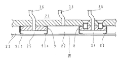
図7は、本実施形態におけるトップリング1を示す縦断面図である。
図7に示すように、本実施形態におけるトップリング1には、弾性パッドが設けられておらず、その代わりに、チャッキングプレート6の外縁近傍の下面のみを覆うように弾性膜からなるシールリング42が設けられている。また、第1の実施形態とは異なり、チャッキングプレート6には半導体ウェハWを吸着する内周部吸着部(図2中の61)又は外周部吸着部(図2中の62)が設けられておらず構造が簡素になっているが、第1の実施形態と同様にチャッキングプレート6に半導体ウェハを吸着する吸着部を設けることとしてもよい。なお、シールリング42は、エチレンプロピレンゴム(EPDM)、ポリウレタンゴム、シリコンゴム等の強度および耐久性に優れたゴム材によって形成されている。
FIG. 7 is a longitudinal sectional view showing the
As shown in FIG. 7, the
シールリング42は、下端面がポリッシング対象物である半導体ウェハWの上面に接するように設けられており、上述の第1の実施形態における弾性パッド4と同様に、チャッキングプレート6とホルダーリング5との間に挟み込まれ固定されている。なお、半導体ウェハWの外縁にはノッチやオリエンテーションフラットと呼ばれる、半導体ウェハの向きを認識(特定)するための切り欠きが設けられているが、このようなノッチやオリエンテーションフラットよりもチャッキングプレート6の内周側にまでシールリング42が延出していることが好ましい。
The seal ring 42 is provided so that the lower end surface is in contact with the upper surface of the semiconductor wafer W that is a polishing target, and the
第1の実施形態と同様に、チャッキングプレート6の下面の中心部にはセンターバッグ8が設けられており、このセンターバッグ8の周囲を取り囲むようにセンターバッグ8の外側にリングチューブ9が設けられている。
As in the first embodiment, a
本実施形態では、研磨される半導体ウェハWが上記シールリング42、センターバッグ8の弾性膜81、及びリングチューブ9の弾性膜91に当接して保持される。従って、第1の実施形態において弾性パッドとチャッキングプレートとによって形成された空間は、半導体ウェハWとチャッキングプレート6とシールリング42によって形成されることとなる。そして、この空間には、上記センターバッグ8及びリングチューブ9によって、センターバッグ8とリングチューブ9の間の圧力室22及びリングチューブ9の外側の圧力室23(第2の圧力室)が形成されている。
In the present embodiment, the semiconductor wafer W to be polished is held in contact with the seal ring 42, the
第1の実施形態と同様に、上記圧力室22、23、センターバッグ8の内部に形成される中心部圧力室24(第1の圧力室)、及びリングチューブ9の内部に形成される中間部圧力室25(第1の圧力室)には、チューブ、コネクタ等からなる流体路33、34、35、36がそれぞれ連通されており、各圧力室22、23、24、25はそれぞれの流体路33〜36上に配置されたレギュレータを介して圧縮空気源に接続されている。これらの圧力室22〜25は、流体路33〜36上に配置された各レギュレータによってそれぞれの圧力室に供給される加圧流体の圧力を調整することができる。これにより各圧力室22〜25の内部の圧力を各々独立に制御する又は大気圧や真空にすることができるようになっている。このように、各圧力室22〜25の内部の圧力を独立に可変とすることにより、半導体ウェハWを研磨パッドに押圧する研磨圧力を半導体ウェハWの部分ごとに調整することができる。なお、場合によっては、これらの圧力室22〜25を真空源121に接続することとしてもよい。
Similar to the first embodiment, the
次に、本実施形態におけるトップリング1の作用について説明する。なお、特に説明しない部分については第1の実施形態と同様である。
半導体ウェハWを吸着する際には、センターバッグ8及びリングチューブ9の内部に所定の圧力の加圧流体を供給して、センターバッグ8及びリングチューブ9の下端面を半導体ウェハWに密着させる。その後、圧力室22及び23をそれぞれ流体路33及び34を介して真空源に接続することにより、圧力室22及び23の内部を負圧にし、圧力室22、23の吸引作用により半導体ウェハWを真空吸着する。
Next, the operation of the
When adsorbing the semiconductor wafer W, a pressurized fluid having a predetermined pressure is supplied into the
また、半導体ウェハWを研磨する際には、トップリング1の下面に半導体ウェハWを保持させると共に、トップリング1の下端に固定されたリテーナリング3を所定の押圧力で研磨テーブルの研磨面に押圧する。この状態で、圧力室22、23、中心部圧力室24、及び中間部圧力室25にそれぞれ所定の圧力の加圧流体を供給し、半導体ウェハWを研磨テーブルの研磨面に押圧する。そして、研磨液供給ノズルから供給される研磨液が半導体ウェハWの研磨される面(下面)と研磨面との間に存在した状態で研磨が行われる。
Further, when polishing the semiconductor wafer W, the semiconductor wafer W is held on the lower surface of the
ここで、半導体ウェハWの圧力室22及び23の下方に位置する部分は、それぞれ圧力室22、23に供給される加圧流体の圧力で研磨面に押圧される。また、半導体ウェハWの中心部圧力室24の下方に位置する部分は、センターバッグ8の弾性膜81を介して中心部圧力室24に供給される加圧流体の圧力で研磨面に押圧される。半導体ウェハWの中間部圧力室25の下方に位置する部分は、リングチューブ9の弾性膜91を介して中間部圧力室25に供給される加圧流体の圧力で研磨面に押圧される。
Here, the portions of the semiconductor wafer W located below the
従って、半導体ウェハWに加わる研磨圧力は、各圧力室22〜25に供給される加圧流体の圧力をそれぞれ制御することにより、半導体ウェハWの部分ごとに調整することができる。このように、半導体ウェハWを同心の4つの円及び円環部分に区切り、それぞれの部分を独立した押圧力で押圧することができる。研磨レートは半導体ウェハWの研磨面に対する押圧力に依存するが、上述したように各部分の押圧力を制御することができるので、半導体ウェハWの4つの部分の研磨レートを独立に制御することが可能となる。従って、半導体ウェハWの表面の研磨すべき薄膜の膜厚に半径方向の分布があっても、半導体ウェハ全面に亘って研磨の不足や過研磨をなくすことができる。即ち、半導体ウェハWの表面の研磨すべき薄膜が、半導体ウェハWの半径方向の位置によって膜厚が異なっている場合であっても、上記各圧力室22〜25のうち、半導体ウェハWの表面の膜厚の厚い部分の上方に位置する圧力室の圧力を他の圧力室の圧力よりも高くすることにより、あるいは、半導体ウェハWの表面の膜厚の薄い部分の上方に位置する圧力室の圧力を他の圧力室の圧力よりも低くすることにより、膜厚の厚い部分の研磨面への押圧力を膜厚の薄い部分の研磨面への押圧力より大きくすることが可能となり、その部分の研磨レートを選択的に高めることができる。これにより、成膜時の膜厚分布に依存せずに半導体ウェハWの全面に亘って過不足のない研磨が可能となる。
Therefore, the polishing pressure applied to the semiconductor wafer W can be adjusted for each portion of the semiconductor wafer W by controlling the pressure of the pressurized fluid supplied to each pressure chamber 22-25. In this way, the semiconductor wafer W can be divided into four concentric circles and annulus parts, and each part can be pressed with an independent pressing force. Although the polishing rate depends on the pressing force on the polishing surface of the semiconductor wafer W, the pressing force of each part can be controlled as described above, so that the polishing rate of the four parts of the semiconductor wafer W can be controlled independently. Is possible. Therefore, even if the film thickness of the thin film to be polished on the surface of the semiconductor wafer W has a radial distribution, it is possible to eliminate insufficient polishing and overpolishing over the entire surface of the semiconductor wafer. That is, even if the thin film to be polished on the surface of the semiconductor wafer W has a different thickness depending on the position in the radial direction of the semiconductor wafer W, the surface of the semiconductor wafer W among the
なお、研磨時には、シールリング42は半導体ウェハWの裏面に密着するため、圧力室23内の加圧流体が外部に漏れることはほとんどない。同様の理由で、センターバッグ8の弾性膜81及びリングチューブ9の弾性膜91の下面に貫通孔を設けたとしても、研磨時に、圧力室24及び25内の加圧流体が外部に漏れることはほとんどない。
At the time of polishing, since the seal ring 42 is in close contact with the back surface of the semiconductor wafer W, the pressurized fluid in the
研磨の終了後は、上述と同様の吸着方法で半導体ウェハWを真空吸着し、圧力室21内の圧力を大気圧に開放するか、もしくは負圧にする。半導体ウェハWを吸着させた後、トップリング1の全体を半導体ウェハの移送位置に位置させ、流体路33及び流体路34を介して半導体ウェハWに流体(例えば、圧縮空気もしくは窒素と純水を混合したもの)を噴射して半導体ウェハWをリリースする。この場合において、センターバッグ8の弾性膜81及びリングチューブ9の弾性膜91の下面に貫通孔を設けた場合には、この貫通孔からも半導体ウェハWに下方向の圧力が加わるため、半導体ウェハWのリリースがよりスムーズになる。また、本実施形態においては半導体ウェハWのリリース後、チャッキングプレート6の下面の大部分が露出することとなるので、研磨終了後の洗浄が比較的容易にできる。
After the polishing is completed, the semiconductor wafer W is vacuum-sucked by the same suction method as described above, and the pressure in the
ここで、本実施形態の基板保持装置におけるセンターバッグ8及びリングチューブ9の他の実施例について説明する。図8は本発明の他の実施例を示す部分縦断面図、図9は半導体ウェハWを取り外した状態における図8の底面図である。この実施例では、図8及び図9に示すように、センターバッグ8の弾性膜81はその外周縁部にのみ設けられており、センターバッグ8の弾性膜81の下面に円形の孔(連通部)83が形成されている。一方、リングチューブ9は2つの弾性膜、即ち、内側の弾性膜91e及び外側の弾性膜91fを備えており、これらの内側弾性膜91eと外側弾性膜91fとの間には環状の溝(連通部)93が形成されている。このような円形孔83及び環状溝93を介して、中心部圧力室24及び中間部圧力室25に供給される加圧流体が当接面である半導体ウェハWの上面に接触することとなる。
Here, another example of the
上述したように、中心部圧力室24や中間部圧力室25に供給される加圧流体の温度を制御し、被研磨面の裏側から半導体ウェハWの温度を制御する場合においては、このような連通部83、93をセンターバッグ8の弾性膜及びリングチューブ9の弾性膜の下面に形成することによって、温度制御された加圧流体が半導体ウェハWに接触する面積を増やすことができるので、半導体ウェハWの温度制御性を向上させることができる。また、研磨終了後、半導体ウェハWをリリースする際には、上記円形孔83及び環状溝93を介して中心部圧力室24及び中間部圧力室25がそれぞれ外気に開放されることとなるので、中心部圧力室24及び中間部圧力室25に供給された流体などがその内部にこもることがない。従って、連続して半導体ウェハWを研磨する場合においても温度制御の安定性を保つことができる。
As described above, when controlling the temperature of the pressurized fluid supplied to the
なお、研磨中は、中心部圧力室24及び中間部圧力室25に加圧流体が供給されるため、この加圧流体により、センターバッグ8の弾性膜81、リングチューブ9の内側弾性膜91e及び外側弾性膜91fの下面が当接面である半導体ウェハWの上面に押し付けられる。従って、このような円形孔83や環状溝93が弾性膜で形成されている場合であっても、中心部圧力室24及び中間部圧力室25の内部の加圧流体が外部に漏れることはほとんどない。
During the polishing, the pressurized fluid is supplied to the
図8及び図9に示す例では、センターバッグ8の弾性膜81には中心部圧力室24に供給された加圧流体によって円形孔83を外方に押し広げようとする力が作用し、リングチューブ9の弾性膜91e、91fには中間部圧力室25に供給された加圧流体によって環状溝93の幅を広げようとする力が作用する。図10に示すように、センターバッグ8の弾性膜81及びリングチューブ9の弾性膜91の下面に、それぞれ複数の円形孔(連通部)84、94を形成すれば、このような加圧流体による力を分散させることができる。
In the example shown in FIGS. 8 and 9, the
また、図11に示すように、センターバッグ8の弾性膜81の下端に、内部に流体が密封された環状の接触部85を形成してもよい。また、リングチューブ9の弾性膜91の下端にそれぞれ内部に流体が密封された環状の(内側)接触部95aと(外側)接触部95bを形成してもよい。この場合において、圧力室21に加圧流体を供給することによって各接触部85、95a、95bが半導体ウェハWに押し付けられ、接触部85、95a、95bによって圧力室22、23、中央部圧力室24、及び中間部圧力室25がそれぞれシールされる。このとき、半導体ウェハWに押し付けられることによって接触部85、95a、95bが変形して接触部85、95a、95bと半導体ウェハWとの接触面積が増え、半導体ウェハWにかかる力が大きくなるが、圧力室21の内部圧力を調整すれば、接触部85、95a、95bによって半導体ウェハWに過剰な力がかかることがないようにすることができる。なお、図8乃至図11に示した実施例は上述した第1の実施形態にも適用できることは言うまでもない。
Further, as shown in FIG. 11, an
次に、本発明に係る基板保持装置の第3の実施形態について図面を参照して詳細に説明する。なお、上述の第2の実施形態における部材又は要素と同一の作用又は機能を有する部材又は要素には同一の符号を付し、特に説明しない部分については第2の実施形態と同様である。 Next, a third embodiment of the substrate holding apparatus according to the present invention will be described in detail with reference to the drawings. In addition, the same code | symbol is attached | subjected to the member or element which has the same effect | action or function as the member or element in the above-mentioned 2nd Embodiment, and the part which is not demonstrated in particular is the same as that of 2nd Embodiment.
図12は本実施形態におけるトップリング1を示す縦断面図、図13は半導体ウェハWを取り外した状態における図12のトップリング1の底面図である。図12に示すように、本実施形態におけるトップリング1には、弾性パッド及びシールリングが設けられていない。
12 is a longitudinal sectional view showing the
本実施形態におけるセンターバッグ8のセンターバッグホルダー82は、図13に示すように、円環形状をなしており、その外周部に円環状の弾性膜81が保持されている。このセンターバッグ8の弾性膜81には、図8及び図9に示す例と同様に、その下面に円形孔83が形成されている。
As shown in FIG. 13, the
本実施形態におけるリングチューブ9は半導体ウェハWの外周縁部に対応する位置に取付けられている。リングチューブ9は、図8及び図9に示した例と同様に、内側弾性膜91e及び外側弾性膜91fを備えており、これらの内側弾性膜91eと外側弾性膜91fとの間に環状溝93が形成されている。また、リングチューブホルダー92の内周側には環状の補助ホルダー96が配置されている。リングチューブ9の内側弾性膜91eの上部は内周側に延出しており、この延出部分をこの補助ホルダー96によって保持することで内側弾性膜91eの保持がより確実になされる。
The
また、センターバッグ8の弾性膜81には、その下面の外周縁から外周側に張り出したつば81bが設けられ、リングチューブ9の内側弾性膜91eには、その下面の内周縁から内周側に張り出したつば91gが設けられている。このようなつば81b、91gを設けることによって、図5に示した実施例で説明したように、各圧力室の圧力制御の幅を更に大きくすることができ、半導体ウェハWの押圧をより安定的に行なうことが可能となる。
Further, the
チャッキングプレート6には、第1の実施形態と同様に、半導体ウェハWを吸着するための内周部吸着部61及び外周部吸着部62が設けられている。内周部吸着部61はセンターバッグ8の内側に、外周部吸着部62はセンターバッグ8とリングチューブ9との間に配置されている。
Similar to the first embodiment, the chucking
本実施形態では、研磨される半導体ウェハWがセンターバッグ8の弾性膜81及びリングチューブ9の弾性膜91e、91fに当接した状態で保持される。従って、半導体ウェハWとチャッキングプレート6との間の空間には、センターバッグ8及びリングチューブ9によって、センターバッグ8とリングチューブ9との間に圧力室22が形成されている。上述したように、リングチューブ9は半導体ウェハWの外周縁部に対応する位置に取付けられており、リングチューブ9の外側に圧力室(図7の符号23)が形成されていない点で第2の実施形態と異なる。
In this embodiment, the semiconductor wafer W to be polished is held in contact with the
チャッキングプレート6の上方に形成される圧力室21、圧力室22、センターバッグ8の内部に形成される中心部圧力室24、及びリングチューブ9の内部に形成される中間部圧力室25には、チューブ、コネクタ等からなる流体路31、33、35、36がそれぞれ連通されており、各圧力室21、22、24、25はそれぞれの流体路31、33、35、36上に配置されたレギュレータを介して圧縮空気源に接続されている。これらの圧力室21、22、24、25は、流体路31、33、35、36上に配置された各レギュレータによってそれぞれの圧力室に供給される加圧流体の圧力を調整することができる。これにより各圧力室21、22、24、25の内部の圧力を各々独立に制御する又は大気圧や真空にすることができるようになっている。このように、各圧力室21、22、24、25の内部の圧力を独立に可変とすることにより、半導体ウェハWを研磨パッドに押圧する研磨圧力を半導体ウェハWの部分ごとに調整することができる。
There are a
半導体ウェハWの研磨の際には、研磨すべき半導体ウェハWの表面の薄膜の膜厚分布に関わらず、研磨パッド等の弾性変形や研磨面と半導体ウェハWとの間への研磨液の入り込み具合などによって、半導体ウェハWの周縁部付近の均一な研磨が阻害されやすい。本実施形態では、リングチューブ9を半導体ウェハWの外周縁部に対応する位置に取付けると共に、リングチューブ9の幅D1を狭くし、センターバッグ8の直径D2を大きくすることで、半導体ウェハWの周縁部付近の研磨圧力を制御し、このような半導体ウェハWの周縁部付近の不均一な研磨を抑制している。具体的には、リングチューブ9の幅D1は10mm以下、更には、5mm以下であることが好ましい。センターバッグ8とリングチューブ9との間の幅D3は、研磨する半導体ウェハWの直径が200mmの場合には20〜25mm、研磨する半導体ウェハWが300mmの場合には25〜30mmであることが好ましい。
When polishing the semiconductor wafer W, regardless of the film thickness distribution of the thin film on the surface of the semiconductor wafer W to be polished, elastic deformation of the polishing pad or the like, or the polishing liquid enters between the polishing surface and the semiconductor wafer W Depending on the condition, uniform polishing near the peripheral edge of the semiconductor wafer W is likely to be hindered. In the present embodiment, the
さてこれまで本発明の一実施形態について説明したが、本発明は上述の実施形態に限定されず、その技術的思想の範囲内において種々異なる形態にて実施されてもよいことは言うまでもない。 Although one embodiment of the present invention has been described so far, the present invention is not limited to the above-described embodiment, and it is needless to say that the present invention may be implemented in various forms within the scope of the technical idea.
上述の実施形態では、流体路31、33、34、35、36をそれぞれ別個に設けたが、これらの流体路を統合したり、各圧力室同士を連通させたりするなど、半導体ウェハWに加えるべき押圧力の大きさや加える位置により自由に改変することが可能である。
In the above-described embodiment, the
例えば、圧力室22に連通する流体路33及び圧力室23に連通する流体路34をなくし、圧力室22及び圧力室23を圧力室21に連通させ、圧力室21、22、23を1つの圧力室とすることもできる。これにより、圧力室21、22、23の圧力が流体路31からの加圧流体によって同一の圧力に制御される。圧力室22と圧力室23の圧力に差を設ける必要がなく、中心部圧力室24及び中間部圧力室25の圧力が圧力室21、22、23の圧力と比べてそれほど大きくない場合には、このようにすることで、流体路33及び34をなくすことができ流体路の数が減るため、流体路の取り回しが簡素になる。
For example, the
また、第1及び第3の実施形態のように、チャッキングプレート6に内周部吸着部61及び外周部吸着部62を設けた場合には、内周部吸着部61に連通する流体路37と外周部吸着部62に連通する流体路38にそれぞれ真空のみでなく加圧流体も供給できるようにすることにより、内周部吸着部61での半導体ウェハの吸着と圧力室22への加圧流体の供給及び外周部吸着部62での半導体ウェハの吸着と圧力室23への加圧流体の供給とをそれぞれ1つの流路で行なうことが可能となる。これにより、流路33及び34は必要なくなるので、流体路が2つ必要なくなり流体路の数が減るため、流体路の取り回しが簡素になる。
Further, as in the first and third embodiments, when the inner peripheral
また、第1及び第2の実施形態におけるチャッキングプレート6の外周縁部には、弾性膜4又はシールリング42の下部周縁の形状を保持するために、下方に突出する突起63が設けられているが(図2及び図7参照)、弾性膜4又はシールリング42がその材質等により形状の保持を必要としない場合には、このような突起を設けずにチャッキングプレート6を構成することも可能である。図14は、第1の実施形態におけるチャッキングプレート6の突起63を削除した場合のトップリング1を示す縦断面図である。このようにすることで、半導体ウェハWを外周縁部までより一様に加圧することができる。また突起63をなくすことにより、半導体ウェハは、研磨面に存在する大きなうねりに対してより容易に従うことが可能となる。
In addition, a
また、上述した実施形態においては、研磨パッドにより研磨面が形成されることとしたが、これに限られるものではない。例えば、固定砥粒により研磨面を形成してもよい。固定砥粒は、砥粒をバインダ中に固定し板状に形成されたものである。固定砥粒を用いた研磨においては、固定砥粒から自生した砥粒により研磨が進行する。固定砥粒は砥粒とバインダと気孔により構成されており、例えば砥粒には平均粒径0.5μm以下の酸化セリウム(CeO2)、バインダにはエポキシ樹脂を用いる。このような固定砥粒は硬質の研磨面を構成する。また、固定砥粒には、上述した板状のものの他に、薄い固定砥粒層の下に弾性を有する研磨パッドを貼付して二層構造とした固定砥粒パッドも含まれる。その他の硬質の研磨面としては、上述したIC−1000がある。 In the embodiment described above, the polishing surface is formed by the polishing pad. However, the present invention is not limited to this. For example, the polishing surface may be formed by fixed abrasive grains. The fixed abrasive is a plate formed by fixing the abrasive in a binder. In polishing using fixed abrasive grains, polishing proceeds by abrasive grains spontaneously generated from the fixed abrasive grains. The fixed abrasive grains are composed of abrasive grains, a binder, and pores. For example, cerium oxide (CeO 2 ) having an average particle diameter of 0.5 μm or less is used for the abrasive grains, and an epoxy resin is used for the binder. Such fixed abrasive grains constitute a hard polishing surface. The fixed abrasive also includes a fixed abrasive pad having a two-layer structure in which a polishing pad having elasticity is stuck under a thin fixed abrasive layer in addition to the plate-like one described above. Other hard polishing surfaces include the IC-1000 described above.
1 トップリング
2 トップリング本体
2a ハウジング部
2b 加圧シート支持部
2c シール部
2d 球面状凹部
3 リテーナリング
4 弾性パッド
5 ホルダーリング
5a 上端部
5b ストッパ部
5c 突起
6 チャッキングプレート(支持部材)
7 加圧シート
8 センターバッグ(中心部当接部材)
9 リングチューブ(外側当接部材)
10 自在継手部
11 トップリング駆動軸
11a 球面状凹部
12 ベアリングボール
21 圧力室
22、23 圧力室(第2の圧力室)
24 中心部圧力室(第1の圧力室)
25 中間部圧力室(第1の圧力室)
26 空間
31、32、33、34、35、36、37、38 流体路
39 リリーフポート
41 開口部
42 シールリング
51 洗浄液路
52 貫通孔
53、57 連通孔
55、56、58 ネジ
61 内周部吸着部
61a、62a 連通孔
61b、62b 弾性シート
62 外周部吸着部
63 突起
81、91 弾性膜
81a、81b、91a、91g つば
82 センターバッグホルダー(保持部)
82a、92a ネジ穴
82b、92b 連通孔
83、84、94 円形孔(連通部)
85、95a、95b 接触部
91d 非弾性体
91e 内側弾性膜
91f 外側弾性膜
92 リングチューブホルダー(保持部)
93 環状溝(連通部)
96 補助ホルダー
101 研磨パッド
100 研磨テーブル
102 研磨液供給ノズル
110 トップリングヘッド
111 トップリング用エアシリンダ
112 回転筒
113、116 タイミングプーリ
114 トップリング用モータ
115 タイミングベルト
117 トップリングヘッドシャフト
120 圧縮空気源(供給源)
121 真空源
G 間隙
Q 研磨液
R1、R2、R3、R4、R5、R6 レギュレータ
V1、V2 バルブ
W 半導体ウェハ
DESCRIPTION OF
7
9 Ring tube (outer contact member)
DESCRIPTION OF SYMBOLS 10 Universal
24 central pressure chamber (first pressure chamber)
25 Intermediate pressure chamber (first pressure chamber)
26
82a,
85, 95a, 95b Contact portion
93 Annular groove (communication part)
96
121 Vacuum source G Gap Q Polishing liquid R1, R2, R3, R4, R5, R6 Regulator V1, V2 Valve W Semiconductor wafer
Claims (8)
ポリッシング対象物である基板を保持するトップリングとを備えるポリッシング装置であって、
前記トップリングは、トップリング本体を備え、
前記トップリング本体には、前記基板と当接する1枚の弾性パッドと、該弾性パッドを支持し、絶縁性材料からなる支持部材とを備え、前記支持部材の下面が前記1枚の弾性パッドによって覆うようにされることによって該支持部材と該弾性パッドとの間に空間が形成され、該空間は内部で分割されて前記1枚の弾性パッドの上面に加圧流体の圧力が直接印加される複数の圧力室が形成されるように構成されており、
前記ポリッシング装置は、前記基板が前記トップリングに保持された状態で、渦電流を用いて前記基板に形成された薄膜の膜厚を測定し、該膜厚の厚い部分の研磨面への押圧力が該膜厚の薄い部分の研磨面への押圧力よりも大きくすることにより選択的に膜厚の厚い部分の研磨速度を高くするように前記複数の圧力室の圧力を制御しうるようにされたことを特徴とするポリッシング装置。 A polishing table having a polishing surface;
A polishing apparatus comprising a top ring for holding a substrate which is a polishing object,
The top ring includes a top ring body,
The top ring to the body, one of the elastic pad to contact with the substrate, and supporting the elastic pad, and a support member made of an insulating material, the elastic pad bottom surface of one said of said supporting member A space is formed between the support member and the elastic pad, and the space is divided inside so that the pressure of the pressurized fluid is directly applied to the upper surface of the one elastic pad. A plurality of pressure chambers are formed,
The polishing apparatus measures the film thickness of a thin film formed on the substrate using eddy current in a state where the substrate is held on the top ring, and presses the thick portion on the polishing surface. However, the pressure in the plurality of pressure chambers can be controlled so as to selectively increase the polishing rate of the thick part by increasing the pressing force of the thin part on the polishing surface. A polishing apparatus characterized by that.
Priority Applications (1)
| Application Number | Priority Date | Filing Date | Title |
|---|---|---|---|
| JP2007071591A JP4620072B2 (en) | 2000-10-11 | 2007-03-19 | Polishing device |
Applications Claiming Priority (2)
| Application Number | Priority Date | Filing Date | Title |
|---|---|---|---|
| JP2000311071 | 2000-10-11 | ||
| JP2007071591A JP4620072B2 (en) | 2000-10-11 | 2007-03-19 | Polishing device |
Related Parent Applications (1)
| Application Number | Title | Priority Date | Filing Date |
|---|---|---|---|
| JP2001013899A Division JP2002187060A (en) | 2000-10-11 | 2001-01-22 | Substrate holding device, polishing device and grinding method |
Related Child Applications (1)
| Application Number | Title | Priority Date | Filing Date |
|---|---|---|---|
| JP2009266388A Division JP2010045408A (en) | 2000-10-11 | 2009-11-24 | Polishing method and equipment |
Publications (3)
| Publication Number | Publication Date |
|---|---|
| JP2007208282A JP2007208282A (en) | 2007-08-16 |
| JP2007208282A5 JP2007208282A5 (en) | 2009-08-06 |
| JP4620072B2 true JP4620072B2 (en) | 2011-01-26 |
Family
ID=38487412
Family Applications (1)
| Application Number | Title | Priority Date | Filing Date |
|---|---|---|---|
| JP2007071591A Expired - Lifetime JP4620072B2 (en) | 2000-10-11 | 2007-03-19 | Polishing device |
Country Status (1)
| Country | Link |
|---|---|
| JP (1) | JP4620072B2 (en) |
Families Citing this family (1)
| Publication number | Priority date | Publication date | Assignee | Title |
|---|---|---|---|---|
| KR102307563B1 (en) * | 2015-05-06 | 2021-10-05 | 주식회사 케이씨텍 | Carrier for substrate and chemical mechanical polishing apparatus having the same |
Citations (8)
| Publication number | Priority date | Publication date | Assignee | Title |
|---|---|---|---|---|
| JPH07122523A (en) * | 1993-10-28 | 1995-05-12 | Toshiba Corp | Semiconductor production system |
| JPH08285514A (en) * | 1995-04-10 | 1996-11-01 | Internatl Business Mach Corp <Ibm> | Method for monitoring change in film thickness on spot thereof |
| JPH10180627A (en) * | 1996-11-08 | 1998-07-07 | Applied Materials Inc | Supporting head having flexible film for chemical and mechanical grinding system |
| JPH10202520A (en) * | 1997-01-20 | 1998-08-04 | Tokyo Seimitsu Co Ltd | Wafer thickness processing quantity measuring device |
| JPH11226865A (en) * | 1997-12-11 | 1999-08-24 | Speedfam Co Ltd | Carrier and cmp device |
| JPH11262857A (en) * | 1998-03-18 | 1999-09-28 | Rohm Co Ltd | Polishing device for semiconductor wafer |
| WO2000051782A1 (en) * | 1999-03-03 | 2000-09-08 | Mitsubishi Materials Corporation | Apparatus and method for chemical-mechanical polishing (cmp) using a head having direct pneumatic wafer polishing pressure system |
| JP2000263421A (en) * | 1999-03-11 | 2000-09-26 | Toshiba Mach Co Ltd | Polishing device |
-
2007
- 2007-03-19 JP JP2007071591A patent/JP4620072B2/en not_active Expired - Lifetime
Patent Citations (8)
| Publication number | Priority date | Publication date | Assignee | Title |
|---|---|---|---|---|
| JPH07122523A (en) * | 1993-10-28 | 1995-05-12 | Toshiba Corp | Semiconductor production system |
| JPH08285514A (en) * | 1995-04-10 | 1996-11-01 | Internatl Business Mach Corp <Ibm> | Method for monitoring change in film thickness on spot thereof |
| JPH10180627A (en) * | 1996-11-08 | 1998-07-07 | Applied Materials Inc | Supporting head having flexible film for chemical and mechanical grinding system |
| JPH10202520A (en) * | 1997-01-20 | 1998-08-04 | Tokyo Seimitsu Co Ltd | Wafer thickness processing quantity measuring device |
| JPH11226865A (en) * | 1997-12-11 | 1999-08-24 | Speedfam Co Ltd | Carrier and cmp device |
| JPH11262857A (en) * | 1998-03-18 | 1999-09-28 | Rohm Co Ltd | Polishing device for semiconductor wafer |
| WO2000051782A1 (en) * | 1999-03-03 | 2000-09-08 | Mitsubishi Materials Corporation | Apparatus and method for chemical-mechanical polishing (cmp) using a head having direct pneumatic wafer polishing pressure system |
| JP2000263421A (en) * | 1999-03-11 | 2000-09-26 | Toshiba Mach Co Ltd | Polishing device |
Also Published As
| Publication number | Publication date |
|---|---|
| JP2007208282A (en) | 2007-08-16 |
Similar Documents
| Publication | Publication Date | Title |
|---|---|---|
| KR100874712B1 (en) | Substrate holding apparatus | |
| US7632173B2 (en) | Substrate holding apparatus and polishing apparatus | |
| JP4718107B2 (en) | Substrate holding device and polishing device | |
| JP4107835B2 (en) | Substrate holding device and polishing device | |
| JP3989234B2 (en) | Substrate holding device and polishing device | |
| JP4049579B2 (en) | Substrate holding device and polishing device | |
| JP4620072B2 (en) | Polishing device | |
| JP2010045408A (en) | Polishing method and equipment | |
| JP3856634B2 (en) | Substrate holding device and polishing apparatus provided with the substrate holding device | |
| JP2008066761A (en) | Substrate holding device | |
| JP2007229922A (en) | Substrate holding device and polishing apparatus |
Legal Events
| Date | Code | Title | Description |
|---|---|---|---|
| A521 | Written amendment |
Free format text: JAPANESE INTERMEDIATE CODE: A523 Effective date: 20090622 |
|
| A977 | Report on retrieval |
Free format text: JAPANESE INTERMEDIATE CODE: A971007 Effective date: 20090914 |
|
| A131 | Notification of reasons for refusal |
Free format text: JAPANESE INTERMEDIATE CODE: A131 Effective date: 20090929 |
|
| A521 | Written amendment |
Free format text: JAPANESE INTERMEDIATE CODE: A523 Effective date: 20091124 |
|
| A131 | Notification of reasons for refusal |
Free format text: JAPANESE INTERMEDIATE CODE: A131 Effective date: 20100518 |
|
| A521 | Written amendment |
Free format text: JAPANESE INTERMEDIATE CODE: A523 Effective date: 20100715 |
|
| TRDD | Decision of grant or rejection written | ||
| A01 | Written decision to grant a patent or to grant a registration (utility model) |
Free format text: JAPANESE INTERMEDIATE CODE: A01 Effective date: 20101005 |
|
| A01 | Written decision to grant a patent or to grant a registration (utility model) |
Free format text: JAPANESE INTERMEDIATE CODE: A01 |
|
| A61 | First payment of annual fees (during grant procedure) |
Free format text: JAPANESE INTERMEDIATE CODE: A61 Effective date: 20101027 |
|
| FPAY | Renewal fee payment (event date is renewal date of database) |
Free format text: PAYMENT UNTIL: 20131105 Year of fee payment: 3 |
|
| R150 | Certificate of patent or registration of utility model |
Ref document number: 4620072 Country of ref document: JP Free format text: JAPANESE INTERMEDIATE CODE: R150 Free format text: JAPANESE INTERMEDIATE CODE: R150 |
|
| R250 | Receipt of annual fees |
Free format text: JAPANESE INTERMEDIATE CODE: R250 |
|
| R250 | Receipt of annual fees |
Free format text: JAPANESE INTERMEDIATE CODE: R250 |
|
| R250 | Receipt of annual fees |
Free format text: JAPANESE INTERMEDIATE CODE: R250 |
|
| R250 | Receipt of annual fees |
Free format text: JAPANESE INTERMEDIATE CODE: R250 |
|
| R250 | Receipt of annual fees |
Free format text: JAPANESE INTERMEDIATE CODE: R250 |
|
| R250 | Receipt of annual fees |
Free format text: JAPANESE INTERMEDIATE CODE: R250 |
|
| R250 | Receipt of annual fees |
Free format text: JAPANESE INTERMEDIATE CODE: R250 |
|
| R250 | Receipt of annual fees |
Free format text: JAPANESE INTERMEDIATE CODE: R250 |
|
| EXPY | Cancellation because of completion of term |