JP4536759B2 - Conversion circuit - Google Patents
Conversion circuit Download PDFInfo
- Publication number
- JP4536759B2 JP4536759B2 JP2007210168A JP2007210168A JP4536759B2 JP 4536759 B2 JP4536759 B2 JP 4536759B2 JP 2007210168 A JP2007210168 A JP 2007210168A JP 2007210168 A JP2007210168 A JP 2007210168A JP 4536759 B2 JP4536759 B2 JP 4536759B2
- Authority
- JP
- Japan
- Prior art keywords
- conversion circuit
- voltage
- liquid crystal
- circuit according
- variable resistance
- Prior art date
- Legal status (The legal status is an assumption and is not a legal conclusion. Google has not performed a legal analysis and makes no representation as to the accuracy of the status listed.)
- Expired - Fee Related
Links
Images


Classifications
-
- H—ELECTRICITY
- H03—ELECTRONIC CIRCUITRY
- H03M—CODING; DECODING; CODE CONVERSION IN GENERAL
- H03M1/00—Analogue/digital conversion; Digital/analogue conversion
- H03M1/66—Digital/analogue converters
- H03M1/68—Digital/analogue converters with conversions of different sensitivity, i.e. one conversion relating to the more significant digital bits and another conversion to the less significant bits
-
- G—PHYSICS
- G09—EDUCATION; CRYPTOGRAPHY; DISPLAY; ADVERTISING; SEALS
- G09G—ARRANGEMENTS OR CIRCUITS FOR CONTROL OF INDICATING DEVICES USING STATIC MEANS TO PRESENT VARIABLE INFORMATION
- G09G3/00—Control arrangements or circuits, of interest only in connection with visual indicators other than cathode-ray tubes
- G09G3/20—Control arrangements or circuits, of interest only in connection with visual indicators other than cathode-ray tubes for presentation of an assembly of a number of characters, e.g. a page, by composing the assembly by combination of individual elements arranged in a matrix no fixed position being assigned to or needed to be assigned to the individual characters or partial characters
- G09G3/34—Control arrangements or circuits, of interest only in connection with visual indicators other than cathode-ray tubes for presentation of an assembly of a number of characters, e.g. a page, by composing the assembly by combination of individual elements arranged in a matrix no fixed position being assigned to or needed to be assigned to the individual characters or partial characters by control of light from an independent source
- G09G3/36—Control arrangements or circuits, of interest only in connection with visual indicators other than cathode-ray tubes for presentation of an assembly of a number of characters, e.g. a page, by composing the assembly by combination of individual elements arranged in a matrix no fixed position being assigned to or needed to be assigned to the individual characters or partial characters by control of light from an independent source using liquid crystals
- G09G3/3611—Control of matrices with row and column drivers
- G09G3/3685—Details of drivers for data electrodes
- G09G3/3688—Details of drivers for data electrodes suitable for active matrices only
-
- G—PHYSICS
- G09—EDUCATION; CRYPTOGRAPHY; DISPLAY; ADVERTISING; SEALS
- G09G—ARRANGEMENTS OR CIRCUITS FOR CONTROL OF INDICATING DEVICES USING STATIC MEANS TO PRESENT VARIABLE INFORMATION
- G09G2310/00—Command of the display device
- G09G2310/02—Addressing, scanning or driving the display screen or processing steps related thereto
- G09G2310/0264—Details of driving circuits
- G09G2310/027—Details of drivers for data electrodes, the drivers handling digital grey scale data, e.g. use of D/A converters
-
- G—PHYSICS
- G09—EDUCATION; CRYPTOGRAPHY; DISPLAY; ADVERTISING; SEALS
- G09G—ARRANGEMENTS OR CIRCUITS FOR CONTROL OF INDICATING DEVICES USING STATIC MEANS TO PRESENT VARIABLE INFORMATION
- G09G2320/00—Control of display operating conditions
- G09G2320/02—Improving the quality of display appearance
- G09G2320/0257—Reduction of after-image effects
-
- G—PHYSICS
- G09—EDUCATION; CRYPTOGRAPHY; DISPLAY; ADVERTISING; SEALS
- G09G—ARRANGEMENTS OR CIRCUITS FOR CONTROL OF INDICATING DEVICES USING STATIC MEANS TO PRESENT VARIABLE INFORMATION
- G09G2320/00—Control of display operating conditions
- G09G2320/02—Improving the quality of display appearance
- G09G2320/0271—Adjustment of the gradation levels within the range of the gradation scale, e.g. by redistribution or clipping
- G09G2320/0276—Adjustment of the gradation levels within the range of the gradation scale, e.g. by redistribution or clipping for the purpose of adaptation to the characteristics of a display device, i.e. gamma correction
-
- G—PHYSICS
- G09—EDUCATION; CRYPTOGRAPHY; DISPLAY; ADVERTISING; SEALS
- G09G—ARRANGEMENTS OR CIRCUITS FOR CONTROL OF INDICATING DEVICES USING STATIC MEANS TO PRESENT VARIABLE INFORMATION
- G09G3/00—Control arrangements or circuits, of interest only in connection with visual indicators other than cathode-ray tubes
- G09G3/20—Control arrangements or circuits, of interest only in connection with visual indicators other than cathode-ray tubes for presentation of an assembly of a number of characters, e.g. a page, by composing the assembly by combination of individual elements arranged in a matrix no fixed position being assigned to or needed to be assigned to the individual characters or partial characters
- G09G3/34—Control arrangements or circuits, of interest only in connection with visual indicators other than cathode-ray tubes for presentation of an assembly of a number of characters, e.g. a page, by composing the assembly by combination of individual elements arranged in a matrix no fixed position being assigned to or needed to be assigned to the individual characters or partial characters by control of light from an independent source
- G09G3/36—Control arrangements or circuits, of interest only in connection with visual indicators other than cathode-ray tubes for presentation of an assembly of a number of characters, e.g. a page, by composing the assembly by combination of individual elements arranged in a matrix no fixed position being assigned to or needed to be assigned to the individual characters or partial characters by control of light from an independent source using liquid crystals
- G09G3/3611—Control of matrices with row and column drivers
- G09G3/3614—Control of polarity reversal in general
-
- H—ELECTRICITY
- H03—ELECTRONIC CIRCUITRY
- H03M—CODING; DECODING; CODE CONVERSION IN GENERAL
- H03M1/00—Analogue/digital conversion; Digital/analogue conversion
- H03M1/66—Digital/analogue converters
- H03M1/74—Simultaneous conversion
- H03M1/80—Simultaneous conversion using weighted impedances
- H03M1/802—Simultaneous conversion using weighted impedances using capacitors, e.g. neuron-mos transistors, charge coupled devices
-
- H—ELECTRICITY
- H03—ELECTRONIC CIRCUITRY
- H03M—CODING; DECODING; CODE CONVERSION IN GENERAL
- H03M1/00—Analogue/digital conversion; Digital/analogue conversion
- H03M1/66—Digital/analogue converters
- H03M1/86—Digital/analogue converters with intermediate conversion to frequency of pulses
- H03M1/88—Non-linear conversion
Description
本発明は変換回路に関するもので、特に液晶の光学的特性を補正するガンマカーブに応じた駆動電圧を発生させることのできる、変換回路に関する。 The present invention relates to a conversion circuit , and more particularly to a conversion circuit capable of generating a drive voltage corresponding to a gamma curve for correcting optical characteristics of liquid crystal.
液晶は電圧を変化させることにより駆動されるが、駆動電圧と光学特性の関係は一般に非線形であり、この非線形の関係を補正するためにガンマ電圧として液晶に供給される。 The liquid crystal is driven by changing the voltage, but the relationship between the drive voltage and the optical characteristics is generally non-linear. In order to correct this non-linear relationship, the liquid crystal is supplied to the liquid crystal as a gamma voltage.
このようなガンマ電圧は、低温ポリシリコン(LTPS)液晶ディスプレイにおいては、特許文献1に示されるように、従来はガラスに作り込まれた複数の直列抵抗とここに接続された複数の中間タップから構成される。
In a low-temperature polysilicon (LTPS) liquid crystal display, such a gamma voltage is generated from a plurality of series resistors conventionally formed in glass and a plurality of intermediate taps connected thereto, as shown in
このようにして形成された構成から入力データに対応するガンマ電圧を取り出すことができ、このガンマ電圧は液晶の特性によって決定された電圧カーブをなす。
しかしながら、このような電圧カーブは、露光マスクを用いて作り込まれた固定の直列抵抗の値で決定され、後に変更することはできない。 However, such a voltage curve is determined by a fixed series resistance value built using an exposure mask and cannot be changed later.
したがって、液晶の材質を変えたときには特性は変化するが、このような場合には直列抵抗の値を変えるように露光マスクを作り直さなければならない。 Therefore, the characteristics change when the material of the liquid crystal is changed, but in such a case, the exposure mask must be remade so as to change the value of the series resistance.
さらに、液晶の光学特性自体についても、ユーザの好みによって要求する画質特性も変化するが、従来はそのような要求に応えることができない。また応えるためには異なる特性ごとにガンマ電圧発生器が必要となり、小型化や低コスト化の障害となる。また、一つの設計で種々の製品に対応できるデザインポータビリティが悪く、複数の製品についての共通デザイン化が困難で、結局コスト増につながることになる。 In addition, the optical characteristics of the liquid crystal itself vary depending on the user's preference. However, conventionally, such demands cannot be met. In order to respond, a gamma voltage generator is required for each different characteristic, which is an obstacle to miniaturization and cost reduction. In addition, design portability that can deal with various products in one design is poor, and it is difficult to make a common design for a plurality of products, resulting in an increase in cost.
本発明は、このような問題を解決するためになされたもので、設計変更やユーザの好みに応じて液晶の光学的特性を適切に補正し、かつ小型化、低コスト化、広いデザインポータビリティを達成することのできる変換回路を提供することを目的とする。 The present invention has been made to solve such problems, and appropriately corrects the optical characteristics of the liquid crystal according to the design change and user's preference, and achieves downsizing, cost reduction, and wide design portability. It is an object to provide a conversion circuit that can be achieved.
本発明によれば、
所望の電圧特性カーブデータを記憶する記憶手段と、
選択データに応じて前記記憶手段に記憶された電圧特性カーブデータに応じた周波数信号を発生させる変調手段と、
第1の電源と第2の電源間に接続された可変抵抗手段であって、前記変調手段からの周波数信号により抵抗値が変化する可変抵抗手段と、
前記可変抵抗手段に発生する電圧を保持する保持手段と、
前記選択データに応じて、前記保持手段に保持された前記電圧を出力する出力手段とを備えた変換回路が提供される。
According to the present invention,
Storage means for storing desired voltage characteristic curve data;
Modulation means for generating a frequency signal according to voltage characteristic curve data stored in the storage means according to selection data;
Variable resistance means connected between a first power supply and a second power supply, wherein the resistance value changes according to a frequency signal from the modulation means;
Holding means for holding a voltage generated in the variable resistance means;
A conversion circuit is provided that includes output means for outputting the voltage held in the holding means in accordance with the selection data.
本発明によれば、あらかじめ記憶された特性に応じたガンマ電圧値を変調周波数によって任意に決定することができるため、設計変更やユーザの好みに応じて液晶の光学的特性を適切に補正することができる。 According to the present invention, since the gamma voltage value according to the characteristic stored in advance can be arbitrarily determined by the modulation frequency, the optical characteristic of the liquid crystal is appropriately corrected according to the design change or user preference. Can do.
また、様々なガンマ電圧要求に対してガラス板上の回路の変更の必要がないため、小型化、低コスト化、広いデザインポータビリティを達成することができる。
さらに、単一のガンマ電圧発生回路で、RGB独立駆動やACコモン駆動なども実現でき、高い汎用性を有する。
Further, since there is no need to change the circuit on the glass plate for various gamma voltage requirements, it is possible to achieve downsizing, cost reduction, and wide design portability.
Furthermore, with a single gamma voltage generation circuit, RGB independent drive and AC common drive can be realized, and it has high versatility.
以下、図面を参照して本発明にかかるその実施例のいくつかを説明する。 Several embodiments of the present invention will be described below with reference to the drawings.
本発明を詳細に説明する前に、従来の構成について説明する。 Prior to describing the present invention in detail, a conventional configuration will be described.
図1は典型的な液晶表示装置1の構成を示すもので、画素に対応する液晶セル3がマトリクス状に配設されて表示部をなす液晶セルアレイ2を構成しており、この液晶セルアレイを駆動するためのゲート線駆動回路7、ソース線駆動回路8を有している。
FIG. 1 shows a configuration of a typical liquid
液晶セル3はゲートがゲート線GLに接続され、ソースがソース線SLに接続された薄膜トランジスタ4のトレインと接地間にキャパシタとして表される液晶表示素子5およびこれに並列に接続された蓄積容量6が接続された構成となっている。
The
また、ゲート線駆動回路は各行の液晶セルの各薄膜トランジスタに共通接続されたゲート線GLを行ごとに順次活性化する。さらにソース線駆動回路は各列の液晶セルの各薄膜トランジスタのソースに共通接続されたソース線SLに電圧信号を供給するものである。 Further, the gate line driving circuit sequentially activates the gate lines GL commonly connected to the thin film transistors of the liquid crystal cells in each row for each row. Further, the source line driving circuit supplies a voltage signal to the source line SL commonly connected to the sources of the thin film transistors of the liquid crystal cells in each column.
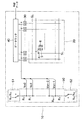
図2は、本発明の適用が予定される従来の液晶表示装置の主要部をなすLCDモジュール10を示しており、このLCDモジュール10は液晶セルがマトリクス状に配設されたセルアレイ20(図1の参照番号2で示されるものに対応)を有し、このセルアレイ20と複数のゲート線GL、および複数のソース線SL、これらの交差部に設けられた薄膜トランジスタ、液晶素子の関係は図1に示した通りである。
FIG. 2 shows an
ゲート線GLにはゲート線駆動回路(図示せず)よりアナログのゲート電圧が順次ゲート線に供給され、各ソース線SLの一端側(図2では上側)にディジタル・アナログ変換器DACが設けられ、このディジタル・アナログ変換器DACには、後述するガンマ電圧発生器50からの電圧信号と外部からのデジタルデータをラッチするデータラッチ40からの信号がそれぞれ入力されるようになっている。
An analog gate voltage is sequentially supplied to the gate line from a gate line driving circuit (not shown) to the gate line GL, and a digital / analog converter DAC is provided on one end side (upper side in FIG. 2) of each source line SL. The digital-analog converter DAC is supplied with a voltage signal from a gamma voltage generator 50 (to be described later) and a signal from a
ガンマ電圧発生器50は電源電圧Vddと接地電圧Vssをいずれか一方を相補的に接続する切換回路51および52の間に(n+1)個の抵抗R0〜RNが直列接続され、中間タップである各抵抗の接続点から、抵抗分割されたn個のガンマ電圧値が取り出されるようになっている。このガンマ電圧値はバスの形で前述したDACに供給され、データラッチからの選択データに応じてDACでディジタル・アナログ変換され、ソース線に供給される。2つの切換回路51および52を反対側に切り換えることにより、抵抗列に印加される電圧は極性が反転し、液晶の駆動極性を反転させることができる。
In the
ここで、従来のガンマ電圧発生器50は複数の直列抵抗とここに接続された複数の中間タップから構成されるために、前述したように、得られるガンマ電圧は固定的なものであった。
Here, since the conventional
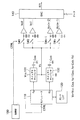
図3は本発明にかかる変換回路の基本的な構成を示すブロック図であり、図2における液晶素子に印加される電圧を供給する構成の大部分を置き換えるものである。 FIG. 3 is a block diagram showing the basic configuration of the conversion circuit according to the present invention, which replaces most of the configuration for supplying the voltage applied to the liquid crystal element in FIG.
制御部100で発生された制御信号CTRLが供給されるモジュレータ110は、その制御信号CTRLの値に応じて所望のガンマ曲線のガンマ値を記憶したガンマルックアップテーブル(LUT)120を参照し、2つの周波数信号faとfbを出力する。これらの周波数信号faとfbは、電源Vccと接地間に直列に接続されたそれぞれ容量CpaとCpbを有する2つのスイッチトキャパシタ131および132に与えられてこれらを制御する。
The
ここで、スイッチトキャパシタの動作について説明する。図4はスイッチトキャパシタ130の基本動作を説明するブロック図であって、図3に示した構成の一部を取り出したものである。一端が接地されたキャパシタCpaの他端を電源電圧Vccおよび定電流Icを発生する電流源に置き換え、周波数faでスイッチング接続するスイッチを設けたものであり、この周波数faは制御信号CTRLにより変調を行うモジュレータにより与えられる。
Here, the operation of the switched capacitor will be described. FIG. 4 is a block diagram for explaining the basic operation of the switched
そして電流源と、電流源側のスイッチの接続点から出力電圧Voutが取り出されるが、その値は、
Vout = Vcc − Ic/(fa*Cpa)
で表され、モジュレータから出力される周波数faを変えることにより、出力電圧を変化させることができる。
The output voltage Vout is extracted from the connection point between the current source and the switch on the current source side.
Vout = Vcc-Ic / (fa * Cpa)
The output voltage can be changed by changing the frequency fa output from the modulator.
なお、低電流源の代わりに固定抵抗でも同じ動作を得ることができる。
図3の構成ではそれぞれ異なる周波数で駆動される2つのスイッチトキャパシタを直列接続したものであり、その接続中点に出力電圧Vsが現れ、次のような値となる。
Vs = Vcc・Cpa・fa/ (Cpa・fa+Cpb・fb)
The same operation can be obtained with a fixed resistor instead of the low current source.
In the configuration of FIG. 3, two switched capacitors driven at different frequencies are connected in series, and the output voltage Vs appears at the midpoint of the connection, and has the following value.
Vs = Vcc * Cpa * fa / (Cpa * fa + Cpb * fb)
この電圧はモジュレータから出力される周波数比fa/fbが変化する周期と同じタイミングにより順次1つずつ閉じるスイッチSW1〜SWnを経てそれぞれスイッチの出力側と接地間に設けられたキャパシタおよびバッファよりなるサンプルホールド回路を介してソース電圧Vo0〜Vo(n−1)としてディジタル・アナログ変換器に与えられる。
なお、スイッチとサンプルホールド回路はソース線に対応して設けられており、ディジタル・アナログ変換器DACではどのガンマ値を選択するかを示すデジタルデータDataにより所望のガンマ値に応じたソース電圧が選択され、このソース電圧がソース線に与えられる。
This voltage is a sample composed of a capacitor and a buffer provided between the output side of the switch and the ground through switches SW1 to SWn that are sequentially closed one by one at the same timing as the cycle in which the frequency ratio fa / fb output from the modulator changes. Source voltages Vo0 to Vo (n-1) are applied to the digital / analog converter via the hold circuit.
The switch and sample hold circuit are provided corresponding to the source line, and the digital / analog converter DAC selects the source voltage corresponding to the desired gamma value by the digital data Data indicating which gamma value is selected. This source voltage is applied to the source line.
図5は変調周波数の変化とそれにより得られるガンマ重み付け出力電圧の関係を示すグラフであり、ガンマルックアップテーブルを参照してモジュレータにより変調された周波数出力faは実線で、周波数出力fbは波線で示されている。ここで、ガンマ曲線を64の値で表すものとすると、nの値を0から63まで変化させると、ルックアップテーブルを参照してガンマ曲線に応じて変調周波数faおよびfbの組み合わせが得られ、前述したVsの式によりガンマ重み付けられた出力電圧Vo0〜Vo(n−1)が得られることを示している。 FIG. 5 is a graph showing the relationship between the change of the modulation frequency and the gamma weighted output voltage obtained thereby. The frequency output fa modulated by the modulator with reference to the gamma lookup table is a solid line, and the frequency output fb is a wavy line. It is shown. Here, assuming that the gamma curve is represented by a value of 64, when the value of n is changed from 0 to 63, a combination of modulation frequencies fa and fb is obtained according to the gamma curve with reference to the lookup table, It shows that gamma-weighted output voltages Vo0 to Vo (n-1) are obtained by the above-described equation for Vs.
図6はデータの値と、これにより参照されるルックアップテーブル120の値に応じてモジュレータから出力される2つの周波数の比fa/fbとの関係をガンマ値=1.8の場合を例にとって説明するグラフである。図5に示されるように、nの数が増加するにしたがって、faは減少、fbは増加するため、周波数比fa/fbはn=0のときの値9が当初は急激に減少し、その後減少の程度が緩慢となって0の値に漸近するような曲線となる。
FIG. 6 shows an example of the relationship between the data value and the ratio fa / fb of the two frequencies output from the modulator in accordance with the value of the lookup table 120 referred to by the case where the gamma value = 1.8. It is a graph to explain. As shown in FIG. 5, as the number of n increases, fa decreases and fb increases, so that the frequency ratio fa / fb initially has a
図7は、データが変化したときの図3における出力電圧Vsの変化を示すグラフである。この出力電圧のうちソース線ごとに指定されたデータnに対応したものが各ソース線に供給されることになる。 FIG. 7 is a graph showing the change in the output voltage Vs in FIG. 3 when the data changes. Of this output voltage, the voltage corresponding to the data n designated for each source line is supplied to each source line.
図8は、3つの色についてそれぞれガンマ重み付け出力電圧を得る、本発明の第2の実施例の構成を示すブロック図であり、図9はその動作を示すグラフである。 FIG. 8 is a block diagram showing the configuration of the second embodiment of the present invention for obtaining gamma weighted output voltages for the three colors, and FIG. 9 is a graph showing the operation thereof.
この実施例では図3に示した構成を3つ設け、これらを選択するためのスイッチSWR、SWG、SWBを設けて、図9に示すように時分割で順次選択するようにしたものである。 In this embodiment, three configurations shown in FIG. 3 are provided, and switches SWR, SWG, and SWB for selecting them are provided, and are sequentially selected in a time division manner as shown in FIG.
図3におけるSW1ないしSWnとキャパシタは、サンプルホールド回路151〜153として表してあり、データに対応して色ごとに求められた電圧出力はそれぞれバッファ161〜163を経てDAC140に供給される。
SW1 to SWn and capacitors in FIG. 3 are represented as sample and hold
1つの色についての動作は図3の場合と全く同じであり、1つの画素についてみれば、3色のそれぞれについて適切なガンマ重み付け出力電圧がソース線に供給されることになる。 The operation for one color is exactly the same as in the case of FIG. 3, and for one pixel, an appropriate gamma weighted output voltage is supplied to the source line for each of the three colors.
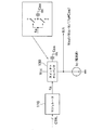
図10は、本発明の第3の実施例の構成を示すブロック図であり、残像現象をなくすためにフレーム毎に極性を反転させるような表示方法に好適なものである。 FIG. 10 is a block diagram showing the configuration of the third embodiment of the present invention, which is suitable for a display method in which the polarity is inverted for each frame in order to eliminate the afterimage phenomenon.
この構成では図3に示した構成と比較して2つのスイッチトキャパシタの代わりに2つのチャージポンプ171,172、これらのチャージポンプ171,172に与えられる電源電圧をVssとVcc間で切り換える切換器200を有し、極性が切り換えられたときに得られるチャージポンプからの出力をそれぞれ選択して出力するためのスイッチSWpおよびSWn、サンプルホールド回路181、182、バッファ191、192を有している。
In this configuration, compared to the configuration shown in FIG. 3, instead of two switched capacitors, two charge pumps 171 and 172, and a
図11は図10に示した第3の実施例における動作を示すグラフである。最初の期間では切換器4でVccが選択されており、図5に示したのと全く同じ減少動作が行われ、ガンマ重み付け出力電圧が得られ、スイッチSWpが閉じられてサンプルホールド回路181およびバッファ191を経て出力される。
FIG. 11 is a graph showing the operation in the third embodiment shown in FIG. In the first period, Vcc is selected by the switch 4 and the same reduction operation as shown in FIG. 5 is performed, a gamma weighted output voltage is obtained, the switch SWp is closed, the
次の期間では、切換器4でVssが選択されるため、極性が反転し、モジュレータ110から出力されるガンマ重み付け出力電圧は負側電圧からnの値が変化するに伴って上昇するものとなる。
In the next period, Vss is selected by the switch 4, so that the polarity is inverted, and the gamma weighted output voltage output from the
この出力電圧は、スイッチSWn、サンプルホールド回路181およびバッファ191を経て出力される。
This output voltage is output through the switch SWn, the
以上説明した実施例は例示したものにすぎず、種々の変形が可能である。 The embodiment described above is merely an example, and various modifications are possible.
たとえば、透過モードと反射モードについての最適なガンマ電圧を取り出すことが可能である。 For example, it is possible to extract optimum gamma voltages for the transmission mode and the reflection mode.
以上、液晶表示装置に用いることを前提とした変換回路について説明したが、本発明はこのような変換回路をソース線駆動回路の一部として含む液晶表示装置にも適用されるものである。 The conversion circuit based on the assumption that it is used in a liquid crystal display device has been described above, but the present invention is also applicable to a liquid crystal display device including such a conversion circuit as part of a source line driver circuit.
また、このような液晶表示装置は図12に示すような携帯型電話装置50のディスプレイ装置1として好適であるが、携帯型電話装置に限られることなく、ディジタルカメラ、個人用情報端末装置(PDA)、ノート型コンピュータ、デスクトップコンビュータ、テレビ受像器、車載ディスプレイ、ポータブルDVDプレーヤのいずかのような電子装置に適用されるものである。
Such a liquid crystal display device is suitable as the
10 LCDモジュール
20 セルアレイ
100 制御部
110 モジュレータ
120 ルックアップテーブル
130,131,132 スイッチトキャパシタ
140 ディジタル・アナログ変換器
151,152,153 サンプル・ホールド回路
161,162,163 バッファ
171、172 チャージ・ポンプ
181,182 サンプル・ホールド回路
191,192 バッファ
DESCRIPTION OF
Claims (12)
選択データに応じて前記記憶手段に記憶された電圧特性カーブデータに応じた周波数信号を発生させる変調手段と、
第1の電源と第2の電源間に接続された可変抵抗手段であって、前記変調手段からの周波数信号により抵抗値が変化する可変抵抗手段と、
前記可変抵抗手段に発生する電圧を保持する保持手段と、
前記選択データに応じて、前記保持手段に保持された前記電圧を出力する出力手段とを備えた変換回路。 Storage means for storing desired voltage characteristic curve data;
Modulation means for generating a frequency signal according to voltage characteristic curve data stored in the storage means according to selection data;
Variable resistance means connected between a first power supply and a second power supply, wherein the resistance value changes according to a frequency signal from the modulation means;
Holding means for holding a voltage generated in the variable resistance means;
A conversion circuit comprising: output means for outputting the voltage held in the holding means according to the selection data.
前記ゲート線を駆動するゲート線駆動装置と、
前記ソース線を駆動するソース線駆動装置を備え、前記ソース線駆動装置は請求項1ないし10のいずれかに記載の変換回路を含むことを特徴とする液晶表示装置。 A plurality of gate lines; a plurality of source lines; and a liquid crystal display element array in which a gate is connected to the gate line at each intersection thereof, and a liquid crystal element is connected to a drain of a thin film transistor having a source connected to the source line;
A gate line driving device for driving the gate line;
A liquid crystal display device comprising: a source line driving device for driving the source line, wherein the source line driving device includes the conversion circuit according to claim 1.
Priority Applications (4)
| Application Number | Priority Date | Filing Date | Title |
|---|---|---|---|
| JP2007210168A JP4536759B2 (en) | 2007-08-10 | 2007-08-10 | Conversion circuit |
| TW097129236A TWI368068B (en) | 2007-08-10 | 2008-08-01 | Digital-analog converter circuit and liquid crystal display device and electronic device using the same |
| CN2008101449421A CN101364806B (en) | 2007-08-10 | 2008-08-07 | Digital-analog converter circuit, liquid crystal display device and electronic device |
| US12/188,863 US8022852B2 (en) | 2007-08-10 | 2008-08-08 | Digital-analog converter circuit |
Applications Claiming Priority (1)
| Application Number | Priority Date | Filing Date | Title |
|---|---|---|---|
| JP2007210168A JP4536759B2 (en) | 2007-08-10 | 2007-08-10 | Conversion circuit |
Publications (3)
| Publication Number | Publication Date |
|---|---|
| JP2009044675A JP2009044675A (en) | 2009-02-26 |
| JP2009044675A5 JP2009044675A5 (en) | 2009-11-12 |
| JP4536759B2 true JP4536759B2 (en) | 2010-09-01 |
Family
ID=40346002
Family Applications (1)
| Application Number | Title | Priority Date | Filing Date |
|---|---|---|---|
| JP2007210168A Expired - Fee Related JP4536759B2 (en) | 2007-08-10 | 2007-08-10 | Conversion circuit |
Country Status (4)
| Country | Link |
|---|---|
| US (1) | US8022852B2 (en) |
| JP (1) | JP4536759B2 (en) |
| CN (1) | CN101364806B (en) |
| TW (1) | TWI368068B (en) |
Families Citing this family (6)
| Publication number | Priority date | Publication date | Assignee | Title |
|---|---|---|---|---|
| TWI437532B (en) * | 2011-07-01 | 2014-05-11 | Novatek Microelectronics Corp | Gate driver and display apparatus using the same |
| US8922541B2 (en) * | 2011-11-24 | 2014-12-30 | Panasonic Corporation | Method of driving display device |
| US8890730B2 (en) * | 2013-03-15 | 2014-11-18 | Xilinx, Inc. | Calibration of a switching instant of a switch |
| CN104347047B (en) * | 2014-11-11 | 2016-09-07 | 深圳市华星光电技术有限公司 | Array base palte, display device and driving method thereof |
| US10290573B2 (en) * | 2015-07-02 | 2019-05-14 | Semiconductor Energy Laboratory Co., Ltd. | Semiconductor device and electronic device |
| CN108831528A (en) * | 2018-06-08 | 2018-11-16 | 福州大学 | A kind of full color vision replacement device based on electric touch |
Citations (4)
| Publication number | Priority date | Publication date | Assignee | Title |
|---|---|---|---|---|
| JPH06224758A (en) * | 1992-04-30 | 1994-08-12 | Hewlett Packard Co <Hp> | Analogue / digital converter |
| JP2003022056A (en) * | 2001-07-06 | 2003-01-24 | Nec Corp | Driving circuit and liquid crystal display device |
| JP2003338760A (en) * | 2002-05-17 | 2003-11-28 | Sharp Corp | Digital-to-analog converter, display driver, and display |
| JP2005204306A (en) * | 2004-01-03 | 2005-07-28 | Sharp Corp | Digital/analog converter, display driver and display |
Family Cites Families (4)
| Publication number | Priority date | Publication date | Assignee | Title |
|---|---|---|---|---|
| US7307569B2 (en) * | 2001-03-29 | 2007-12-11 | Quellan, Inc. | Increasing data throughput in optical fiber transmission systems |
| JP3661650B2 (en) * | 2002-02-08 | 2005-06-15 | セイコーエプソン株式会社 | Reference voltage generation circuit, display drive circuit, and display device |
| JP3661651B2 (en) * | 2002-02-08 | 2005-06-15 | セイコーエプソン株式会社 | Reference voltage generation circuit, display drive circuit, and display device |
| US7443330B2 (en) * | 2006-06-08 | 2008-10-28 | Monolithic Power Systems, Inc. | Method of 1-bit hysteretic control in N-bit A/D conversion |
-
2007
- 2007-08-10 JP JP2007210168A patent/JP4536759B2/en not_active Expired - Fee Related
-
2008
- 2008-08-01 TW TW097129236A patent/TWI368068B/en not_active IP Right Cessation
- 2008-08-07 CN CN2008101449421A patent/CN101364806B/en not_active Expired - Fee Related
- 2008-08-08 US US12/188,863 patent/US8022852B2/en not_active Expired - Fee Related
Patent Citations (4)
| Publication number | Priority date | Publication date | Assignee | Title |
|---|---|---|---|---|
| JPH06224758A (en) * | 1992-04-30 | 1994-08-12 | Hewlett Packard Co <Hp> | Analogue / digital converter |
| JP2003022056A (en) * | 2001-07-06 | 2003-01-24 | Nec Corp | Driving circuit and liquid crystal display device |
| JP2003338760A (en) * | 2002-05-17 | 2003-11-28 | Sharp Corp | Digital-to-analog converter, display driver, and display |
| JP2005204306A (en) * | 2004-01-03 | 2005-07-28 | Sharp Corp | Digital/analog converter, display driver and display |
Also Published As
| Publication number | Publication date |
|---|---|
| JP2009044675A (en) | 2009-02-26 |
| US20090040164A1 (en) | 2009-02-12 |
| CN101364806B (en) | 2012-10-31 |
| TW200907473A (en) | 2009-02-16 |
| CN101364806A (en) | 2009-02-11 |
| TWI368068B (en) | 2012-07-11 |
| US8022852B2 (en) | 2011-09-20 |
Similar Documents
| Publication | Publication Date | Title |
|---|---|---|
| TW517170B (en) | Driving circuit of electro-optical device, and driving method for electro-optical device | |
| US7071669B2 (en) | Reference voltage generation circuit, display driver circuit, display device, and method of generating reference voltage | |
| KR100536871B1 (en) | Display driving device and display using the same | |
| US7106321B2 (en) | Reference voltage generation circuit, display drive circuit, display device and reference voltage generation method | |
| JP4193771B2 (en) | Gradation voltage generation circuit and drive circuit | |
| US7079127B2 (en) | Reference voltage generation circuit, display driver circuit, display device, and method of generating reference voltage | |
| US8730223B2 (en) | Source driver and display device having the same | |
| US6873312B2 (en) | Liquid crystal display apparatus, driving method therefor, and display system | |
| US7330066B2 (en) | Reference voltage generation circuit that generates gamma voltages for liquid crystal displays | |
| US8305321B2 (en) | Apparatus for driving source lines and display apparatus having the same | |
| US20090278865A1 (en) | Source driver and display device including the same | |
| EP1341313A1 (en) | Reference voltage circuit | |
| US20080238842A1 (en) | Liquid crystal device, driving circuit for liquid crystal device, method of driving liquid crystal device, and electronic apparatus | |
| KR20040084854A (en) | Driving apparatus and display module | |
| JP4536759B2 (en) | Conversion circuit | |
| US20080316162A1 (en) | Liquid crystal display and driving method thereof | |
| KR100341068B1 (en) | Digital-to-analogue converters, active matrix liquid crystal display using the same, and digital-to-analogue conversion method | |
| JP2008292837A (en) | Display device | |
| JP2009044675A5 (en) | ||
| US7286071B1 (en) | System for displaying images | |
| TWI386903B (en) | Scan driver | |
| JP2002251160A (en) | Display device | |
| KR20030063156A (en) | A plane display device | |
| JP2008109616A (en) | Voltage conversion device having non-linear gain and changeable gain polarity | |
| JP2005181763A (en) | Liquid crystal driving device |
Legal Events
| Date | Code | Title | Description |
|---|---|---|---|
| A977 | Report on retrieval |
Free format text: JAPANESE INTERMEDIATE CODE: A971007 Effective date: 20090629 |
|
| A521 | Written amendment |
Free format text: JAPANESE INTERMEDIATE CODE: A523 Effective date: 20090925 |
|
| A131 | Notification of reasons for refusal |
Free format text: JAPANESE INTERMEDIATE CODE: A131 Effective date: 20100108 |
|
| A521 | Written amendment |
Free format text: JAPANESE INTERMEDIATE CODE: A523 Effective date: 20100408 |
|
| TRDD | Decision of grant or rejection written | ||
| A01 | Written decision to grant a patent or to grant a registration (utility model) |
Free format text: JAPANESE INTERMEDIATE CODE: A01 Effective date: 20100518 |
|
| A01 | Written decision to grant a patent or to grant a registration (utility model) |
Free format text: JAPANESE INTERMEDIATE CODE: A01 |
|
| A61 | First payment of annual fees (during grant procedure) |
Free format text: JAPANESE INTERMEDIATE CODE: A61 Effective date: 20100616 |
|
| FPAY | Renewal fee payment (event date is renewal date of database) |
Free format text: PAYMENT UNTIL: 20130625 Year of fee payment: 3 |
|
| R150 | Certificate of patent or registration of utility model |
Ref document number: 4536759 Country of ref document: JP Free format text: JAPANESE INTERMEDIATE CODE: R150 Free format text: JAPANESE INTERMEDIATE CODE: R150 |
|
| R250 | Receipt of annual fees |
Free format text: JAPANESE INTERMEDIATE CODE: R250 |
|
| R250 | Receipt of annual fees |
Free format text: JAPANESE INTERMEDIATE CODE: R250 |
|
| R250 | Receipt of annual fees |
Free format text: JAPANESE INTERMEDIATE CODE: R250 |
|
| R250 | Receipt of annual fees |
Free format text: JAPANESE INTERMEDIATE CODE: R250 |
|
| R250 | Receipt of annual fees |
Free format text: JAPANESE INTERMEDIATE CODE: R250 |
|
| R250 | Receipt of annual fees |
Free format text: JAPANESE INTERMEDIATE CODE: R250 |
|
| R250 | Receipt of annual fees |
Free format text: JAPANESE INTERMEDIATE CODE: R250 |
|
| LAPS | Cancellation because of no payment of annual fees |