JP4515136B2 - Laser beam irradiation apparatus and method for manufacturing thin film transistor - Google Patents
Laser beam irradiation apparatus and method for manufacturing thin film transistor Download PDFInfo
- Publication number
- JP4515136B2 JP4515136B2 JP2004123375A JP2004123375A JP4515136B2 JP 4515136 B2 JP4515136 B2 JP 4515136B2 JP 2004123375 A JP2004123375 A JP 2004123375A JP 2004123375 A JP2004123375 A JP 2004123375A JP 4515136 B2 JP4515136 B2 JP 4515136B2
- Authority
- JP
- Japan
- Prior art keywords
- laser
- laser beam
- mirror
- semiconductor film
- irradiation
- Prior art date
- Legal status (The legal status is an assumption and is not a legal conclusion. Google has not performed a legal analysis and makes no representation as to the accuracy of the status listed.)
- Expired - Fee Related
Links
Images


Description
本発明は、ビーム照射装置、ビーム照射方法に関する。さらに本発明は、当該装置及び方法を用いた薄膜トランジスタの作製方法に関する。 The present invention relates to a beam irradiation apparatus and a beam irradiation method. Furthermore, the present invention relates to a method for manufacturing a thin film transistor using the apparatus and the method.
近年、表示装置や集積回路等が有する半導体素子として、多結晶半導体膜をチャネル形成領域として有する薄膜トランジスタ(以下、多結晶TFTと表記する)の研究が行われている。表示装置や集積回路の発達に伴い、多結晶TFTのさらなる特性向上が求められている。 In recent years, a thin film transistor (hereinafter referred to as a polycrystalline TFT) having a polycrystalline semiconductor film as a channel formation region has been studied as a semiconductor element included in a display device, an integrated circuit, or the like. With the development of display devices and integrated circuits, further improvements in the characteristics of polycrystalline TFTs are required.
そこで多結晶TFTを得る一手段として、連続発振型レーザと、レーザビーム(レーザ光とも表記する)を走査する手段とを有するレーザ照射装置を用いて、半導体膜を結晶化している(例えば、特許文献1参照)。 Therefore, as one means for obtaining a polycrystalline TFT, a semiconductor film is crystallized using a laser irradiation apparatus having a continuous wave laser and means for scanning a laser beam (also referred to as laser light) (for example, a patent) Reference 1).
またレーザ光を走査させる手段としてガルバノミラー(特許文献2参照)やポリゴンミラー(特許文献3参照)がよく用いられる。これは走査速度を高速化することが容易なためである。これにより、装置の負担を低減させることができる。 Further, a galvanometer mirror (see Patent Document 2) and a polygon mirror (see Patent Document 3) are often used as means for scanning with laser light. This is because it is easy to increase the scanning speed. Thereby, the burden of an apparatus can be reduced.
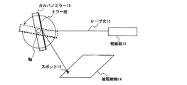
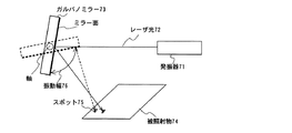
図7には、従来のガルバノミラーの構造を示す。レーザ光の発振器71から出射されるレーザ光72は、ガルバノミラー73で反射し、被照射物74にスポット(照射領域)75を形成する。ガルバノミラー73が振動幅76で振動することにより、スポット75が被照射物上を走査し、レーザ照射処理が行われる。図7に示すガルバノミラーの振動幅にあわせて、レーザ光を被照射物に照射している。 FIG. 7 shows the structure of a conventional galvanometer mirror. The laser beam 72 emitted from the laser beam oscillator 71 is reflected by the galvanometer mirror 73 to form a spot (irradiation region) 75 on the irradiated object 74. When the galvanometer mirror 73 vibrates with the vibration width 76, the spot 75 scans the irradiated object, and laser irradiation processing is performed. The irradiated object is irradiated with laser light in accordance with the vibration width of the galvanometer mirror shown in FIG.
またポリゴンミラーの場合、接して設けられた複数のミラーが回転することで、被照射物にレーザ光を照射している。
特に、大型基板での量産を考える場合、広範囲に渡って均一な結晶性半導体膜を効率よく得ることは重要視されている。そこで、軽量であるため走査速度を高速化することが容易であるガルバノミラーやポリゴンミラーのような走査手段がよく検討されている。またこれら走査手段により、レーザ照射装置の負担を低減させることができる。 In particular, when mass production with a large substrate is considered, it is important to efficiently obtain a uniform crystalline semiconductor film over a wide range. Therefore, a scanning means such as a galvano mirror or a polygon mirror, which is light in weight and can easily increase the scanning speed, has been well studied. Moreover, the burden of a laser irradiation apparatus can be reduced by these scanning means.
しかし、上述のような走査手段を使用すると、レーザ照射面での走査開始及び走査終了といった端部では走査速度や照射状態が不均一になる問題が生じることがあった。またガルバノミラーを振動させると走査幅が蛇行することがあった。 However, when the scanning means as described above is used, there is a problem that the scanning speed and the irradiation state are not uniform at the end portions such as scanning start and scanning end on the laser irradiation surface. Further, when the galvanometer mirror is vibrated, the scanning width sometimes meanders.
例えば、振り子運動(振動)するガルバノミラーにレーザ光が反射して、半導体膜にレーザ照射を行う場合、振り子運動の方向を変える点(振り子運動の頂点、ガルバノミラーの止まり際ともいう)に向かって、速度は減速し、ついには一瞬ゼロになる。その後、運動方向を変えて徐々に速度が加速する。ガルバノミラーの走査速度の減速、加速は短時間で行われるが、より高性能且つ均一な半導体膜の結晶化が要求されるにつれ、このような不均一なレーザ照射、つまり照射ムラは問題となることを見出した。本発明者はこのような照射ムラにより、被照射物に必要以上のエネルギーが照射されてしまうため、非晶質半導体膜に膜剥がれ等が生じる恐れがあることを見出した。膜剥がれが生じてしまうと、飛び散る半導体膜によって、正常な膜まで荒れてしまうことが懸念される。このように、レーザ光の走査速度が不均一になることは、高性能且つ均一な半導体膜の結晶化が要求される半導体分野において問題となる。 For example, when laser light is reflected on a galvanomirror that moves pendulum (vibrates) and the semiconductor film is irradiated with laser light, the point changes the direction of the pendulum movement (also referred to as the apex of the pendulum movement or when the galvanometer mirror stops). The speed slows down and finally goes to zero. After that, the speed is gradually accelerated by changing the direction of motion. Although the scanning speed of the galvanometer mirror is reduced and accelerated in a short time, such non-uniform laser irradiation, that is, irradiation unevenness becomes a problem as higher performance and uniform crystallization of the semiconductor film is required. I found out. The present inventor has found that there is a possibility that film peeling or the like may occur in the amorphous semiconductor film because the irradiation object is irradiated with energy more than necessary due to such irradiation unevenness. When film peeling occurs, there is a concern that a normal film may be roughened by the scattered semiconductor film. As described above, the non-uniform scanning speed of the laser beam becomes a problem in the semiconductor field where high performance and uniform crystallization of the semiconductor film is required.
また回転運動を行う、複数のミラーが連続的に繋がったポリゴンミラーでは、ミラーごとに反射するレーザ光の入射角によって、照射位置がわずかにずれてしまった。特に、ミラーの境界で入射角のずれは、走査開始位置及び走査終了位置のずれを発生させ、不均一なレーザ照射処理の原因となってしまった。また走査方向と垂直な方向にも照射位置がずれるため、これも不均一なレーザ照射処理の原因となってしまった。このような不均一なレーザ光の照射ムラは、より高性能且つ均一な半導体膜の結晶性を得るためには問題となる。 In addition, in the polygon mirror in which a plurality of mirrors that perform rotational movement are continuously connected, the irradiation position is slightly shifted depending on the incident angle of the laser beam reflected for each mirror. In particular, the deviation of the incident angle at the mirror boundary causes a deviation of the scanning start position and the scanning end position, which causes non-uniform laser irradiation processing. In addition, since the irradiation position is shifted in the direction perpendicular to the scanning direction, this also causes non-uniform laser irradiation processing. Such uneven irradiation of the laser beam becomes a problem in order to obtain higher performance and more uniform crystallinity of the semiconductor film.
そこで本発明はガルバノミラー等の走査手段の走査速度を均一とする、又は走査位置を精度よく制御するビーム照射装置、及びビーム照射方法を提供することを課題とする。またさらに、上記のようなビーム照射装置、及びビーム照射方法を用いて薄膜トランジスタ(以下、TFTと表記する)等に対する均一なレーザアニール(結晶化や活性化を含む)を提供することを課題とする。 Therefore, an object of the present invention is to provide a beam irradiation apparatus and a beam irradiation method that make the scanning speed of a scanning unit such as a galvanometer mirror uniform or control the scanning position with high accuracy. It is another object of the present invention to provide uniform laser annealing (including crystallization and activation) for thin film transistors (hereinafter referred to as TFTs) using the beam irradiation apparatus and the beam irradiation method as described above. .
上記問題を鑑み、本発明は単数の鏡面体(ミラーともいう)を有する走査(偏向)手段を利用する場合、当該走査手段を一方向に回転させることを特徴とする。以下、このような鏡面体の例としてガルバノミラーを用いて説明する。 In view of the above problems, the present invention is characterized in that when a scanning (deflecting) means having a single mirror body (also called a mirror) is used, the scanning means is rotated in one direction. Hereinafter, a galvano mirror will be described as an example of such a mirror body.
本発明のガルバノミラーは、一方向に回転させるため回転が安定し、加速度の変化により生じるミラーの振動が排除される。そしてガルバノミラーによるスポットの移動をX軸方向とすると、レーザ光が照射されない位置にガルバノミラーがあるときに、被照射物をX軸方向と直行するY軸方向に移動させるとよい。すると、XY軸方向に走査でき、大面積に対してレーザ照射処理を行うことができる。このときガルバノミラーを一方向に回転させているため、レーザ光は被照射物のX軸上を一方向のみに走査する。 Since the galvanometer mirror of the present invention is rotated in one direction, the rotation is stable, and the vibration of the mirror caused by the change in acceleration is eliminated. When the movement of the spot by the galvano mirror is taken as the X-axis direction, the irradiated object may be moved in the Y-axis direction perpendicular to the X-axis direction when the galvano mirror is at a position where the laser beam is not irradiated. Then, scanning can be performed in the XY axis directions, and laser irradiation processing can be performed on a large area. At this time, since the galvanometer mirror is rotated in one direction, the laser beam scans in only one direction on the X axis of the irradiated object.
具体的には、図1に示すようにガルバノミラー13に設置される軸を中心として、ミラー面が回転する。軸は、一端部又は両端部に支持棒が設けられており、回転を制御する装置が設けられている。両端部に支持棒があると、回転軸がより安定して好ましい。そして、発振器11から射出されるレーザ光12は、ガルバノミラー13に反射して、被照射物14上にスポット15を形成する。このようなガルバノミラー13が回転することにより、スポットが移動し被照射物に対してレーザ照射処理が行われる。 Specifically, as shown in FIG. 1, the mirror surface rotates around an axis installed on the galvano mirror 13. The shaft is provided with a support rod at one end or both ends, and a device for controlling rotation is provided. If there are support rods at both ends, the rotation axis is more stable and preferable. The laser beam 12 emitted from the oscillator 11 is reflected by the galvanometer mirror 13 to form a spot 15 on the irradiated object 14. As the galvano mirror 13 rotates, the spot moves and laser irradiation processing is performed on the irradiated object.
このようにガルバノミラーを回転させ、慣性を利用することで、被照射面におけるスポットの等速性が上がる。また、ガルバノミラーを重くすると、慣性がより強く働くので等速性が向上し好ましい。またガルバノミラーは、簡便且つ小型な構成を採ることができ、レーザ照射装置に搭載する上で好ましい。 Thus, by rotating the galvanometer mirror and utilizing inertia, the constant velocity of the spot on the irradiated surface is increased. Further, it is preferable to make the galvanometer mirror heavy because the inertia works more strongly, so that the constant velocity is improved. Further, the galvanometer mirror can take a simple and small configuration, and is preferable for mounting on a laser irradiation apparatus.
またその他の走査手段として、複数の鏡面体を有する走査手段(簡単のためポリゴンミラーと表記する)が挙げられる。本発明のポリゴンミラーは図2に示すように、複数のミラー27を有し、ミラー間に合わせて、Y軸への走査時間を設けるため、ミラー同士を接して配置しないようにする。そしてレーザ光22は、軸を中心として回転するポリゴンミラー23に入射され、被照射物24上にスポット25が走査する。その結果、被照射物24上にはスポット25が照射されるときと、照射されないときが交互に現れる。すなわちミラー間では、レーザ光が照射されない。このレーザ光が照射されないときと、被照射物の移動とのタイミングを合わせることにより、効率的にレーザ照射処理を行うことができる。つまり、ポリゴンミラーによりX軸方向にスポットを走査させ、スポットが消えている(レーザ光が照射されない)ときに、被照射物をY軸方向に移動させる。このとき、ポリゴンミラーが有するミラー毎に、レーザ光の反射方向が少しずつ異なるため、被照射物のY軸方向への移動量を変えて補正する。その結果、ポリゴンミラーと被照射物との間に補正レンズを配置する必要がなく、レーザ照射装置が簡略化し好ましい。 Other scanning means includes scanning means having a plurality of mirror bodies (referred to as a polygon mirror for simplicity). As shown in FIG. 2, the polygon mirror of the present invention has a plurality of mirrors 27, and in order to provide a scanning time for the Y axis in accordance with the distance between the mirrors, the mirrors are not arranged in contact with each other. The laser beam 22 is incident on a polygon mirror 23 that rotates about an axis, and a spot 25 scans on the irradiated object 24. As a result, when the spot 25 is irradiated and when it is not irradiated appear alternately on the irradiated object 24. That is, no laser light is irradiated between the mirrors. By matching the timing when the laser beam is not irradiated and the movement of the irradiated object, the laser irradiation process can be performed efficiently. That is, the spot is scanned in the X-axis direction by the polygon mirror, and the irradiated object is moved in the Y-axis direction when the spot disappears (no laser light is irradiated). At this time, since the reflection direction of the laser beam is slightly different for each mirror of the polygon mirror, the amount of movement of the irradiated object in the Y-axis direction is changed for correction. As a result, it is not necessary to arrange a correction lens between the polygon mirror and the irradiation object, and the laser irradiation apparatus is simplified and preferable.
このような本発明の走査手段により、被照射物に対して均一なレーザ光の照射を行うことができ、被照射物として半導体膜を用いる場合、結晶性、電気特性の揃った多結晶TFTを形成することができる。 By using the scanning means of the present invention, the irradiated object can be irradiated with uniform laser light. When a semiconductor film is used as the irradiated object, a polycrystalline TFT with uniform crystallinity and electrical characteristics can be obtained. Can be formed.
なお本発明は、連続的に出力されるエネルギービーム(以下、CWビームと表記する)を用いることができる。CWビームとしては、固体レーザを用いればよく、例えばYVO4レーザや、YAGレーザ、YLFレーザ、YAlO3レーザ、Arレーザ等から射出されるビームが当てはまる。またこれらの高調波を使用してもよい。このように、光源としてレーザを使用する場合、CWレーザと表記する。 In the present invention, a continuously output energy beam (hereinafter referred to as a CW beam) can be used. As the CW beam, a solid laser may be used. For example, a beam emitted from a YVO 4 laser, a YAG laser, a YLF laser, a YAlO 3 laser, an Ar laser, or the like is applicable. These harmonics may also be used. Thus, when using a laser as a light source, it describes with CW laser.
なおレーザビームは、任意の形状で構わず、好ましくは光学系を通過することにより線状となるように加工する。なおここでいう「線状」は、厳密な意味で「線」を意味しているのではなく、アスペクト比の大きい長方形(または長楕円形)を意味する。例えば、アスペクト比が10以上(好ましくは100〜10000)のもの指す。具体的には、線状のレーザビームのスポット径は、長軸150〜1000μm、短軸5〜20μmとする。線状に加工されたレーザビームを用いると、スループットの高い処理を行うことができる。 The laser beam may have an arbitrary shape, and is preferably processed so as to be linear by passing through the optical system. Note that “linear” here does not mean “line” in a strict sense, but means a rectangle (or oblong shape) with a large aspect ratio. For example, the aspect ratio is 10 or more (preferably 100 to 10,000). Specifically, the spot diameter of the linear laser beam is set to a major axis of 150 to 1000 μm and a minor axis of 5 to 20 μm. When a laser beam processed into a linear shape is used, processing with high throughput can be performed.
以上のように、本発明は走査手段の動作によって生じるレーザビームの照射の不均一を除去し、結晶性、電気特性の揃った多結晶TFTを提供することができる。さらに大面積な被照射物であっても、広範囲に渡り特性の揃った多結晶TFTを形成することができ、表示装置や集積回路の大量生産性を向上させることができる。 As described above, the present invention can remove the nonuniformity of the laser beam irradiation caused by the operation of the scanning means and provide a polycrystalline TFT having uniform crystallinity and electrical characteristics. Furthermore, even for an object to be irradiated having a large area, a polycrystalline TFT with uniform characteristics can be formed over a wide range, and mass productivity of a display device or an integrated circuit can be improved.
本発明により、被照射物に対して均一なレーザ照射を行うことができ、被照射物として半導体膜を用いる場合、結晶性、電気特性の揃った多結晶TFTを形成することができる。また、被照射物上において、ビームスポットの速度を一定とすることが可能となり、又はスポットの走査位置の制御性も高く、半導体膜に対して一様なレーザアニールを行うことができる。またさらに、大型基板を用いる場合、本発明の高効率なレーザアニールには好適である。 According to the present invention, a uniform laser irradiation can be performed on an object to be irradiated, and when a semiconductor film is used as the object to be irradiated, a polycrystalline TFT having uniform crystallinity and electric characteristics can be formed. In addition, the speed of the beam spot can be made constant on the irradiation object, or the spot scanning position is highly controllable, and uniform laser annealing can be performed on the semiconductor film. Furthermore, when a large substrate is used, it is suitable for the highly efficient laser annealing of the present invention.
また本発明のポリゴンミラーを使用する場合、XYステージの移動距離を各ミラーで設定することにより、さらなる均一なレーザ照射を行うことができる。 When the polygon mirror of the present invention is used, further uniform laser irradiation can be performed by setting the movement distance of the XY stage with each mirror.
以下に、本発明の実施の形態を図面に基づいて説明する。但し、本発明は多くの異なる態様で実施することが可能であり、本発明の趣旨及びその範囲から 逸脱することなくその形態及び詳細を様々に変更し得ることは当業者であれば容易に 理解される。従って、本実施の形態の記載内容に限定して解釈されるものではない。なお、実施の形態を説明するための全図において、同一部分又は同様な機能を有する部分には同一の符号を付し、その繰り返しの説明は省略する。 Embodiments of the present invention will be described below with reference to the drawings. However, it should be understood by those skilled in the art that the present invention can be implemented in many different modes, and that various changes in form and details can be made without departing from the spirit and scope of the present invention. Is done. Therefore, the present invention is not construed as being limited to the description of this embodiment mode. Note that in all the drawings for describing the embodiments, the same portions or portions having similar functions are denoted by the same reference numerals, and repetitive description thereof is omitted.
(実施の形態1)
本実施の形態では、走査手段に回転するガルバノミラーと、被照射物に半導体膜を用い、当該半導体膜を結晶化し、多結晶TFTを形成する場合を説明する。
(Embodiment 1)
In this embodiment mode, a case is described in which a galvanometer mirror that rotates as a scanning unit and a semiconductor film is used as an irradiation object, and the semiconductor film is crystallized to form a polycrystalline TFT.
図3には、CWレーザ(連続発振型レーザとも表記する)を射出する発振器101、発振器より射出されるレーザビームの形状を線状に加工するための光学系102、線状に加工されたレーザビームを半導体膜に走査するためのガルバノミラー、ガルバノミラーを回転させるための軸108、軸を制御し、ガルバノミラーの回転を制御する制御装置110、被照射面でのレーザビームの形状を一定とするためのfθレンズ104、を有するレーザ照射装置を示す。発振器から射出されたレーザビームは、光学系に入射して線状レーザビーム(以下、線状ビームと表記する)に加工され、回転するガルバノミラーへ入射し、ガルバノミラーにより反射し、fθレンズを介して被照射物へ照射される。以上のような機能を有するものによって、レーザビームの照射が制御される。 3 shows an oscillator 101 that emits a CW laser (also referred to as a continuous wave laser), an optical system 102 that processes the shape of a laser beam emitted from the oscillator into a linear shape, and a laser that is processed into a linear shape. Galvano mirror for scanning the semiconductor film, axis 108 for rotating the galvano mirror, controller 110 for controlling the axis and controlling the rotation of the galvano mirror, the shape of the laser beam on the irradiated surface is constant 1 shows a laser irradiation apparatus having an fθ lens 104 for the purpose. The laser beam emitted from the oscillator is incident on an optical system, processed into a linear laser beam (hereinafter referred to as a linear beam), incident on a rotating galvanometer mirror, reflected by the galvanometer mirror, and an fθ lens. The irradiated object is irradiated through. The laser beam irradiation is controlled by the above function.
光学系102には例えば、焦点距離50mmの平凹レンズと、焦点距離200mmの平凸レンズを配置し、さらに平凸レンズの後方に、焦点距離250mmの平凸シリンドリカルレンズを配置し、さらに平凸シリンドリカルレンズの後方に焦点距離100mmの平凹シリンドリカルレンズを配置する。なお、平凸シリンドリカルレンズと平凹シリンドリカルレンズの曲率の方向は同じとする。このような光学系を通過することにより、レーザビームは集光等を繰り返し、線状ビームが加工される。なお、上記レンズ以外のレンズを配置してもよく、照射面においてレーザビームのスポット(ビームスポットとも表記する)が所望の照射形状(例えば線状)となるように配置すればよい。 For example, a plano-concave lens with a focal length of 50 mm and a plano-convex lens with a focal length of 200 mm are arranged in the optical system 102, and a plano-convex cylindrical lens with a focal length of 250 mm is arranged behind the plano-convex lens. A plano-concave cylindrical lens having a focal length of 100 mm is disposed behind. The direction of curvature of the plano-convex cylindrical lens and the plano-concave cylindrical lens are the same. By passing through such an optical system, the laser beam is repeatedly focused and the linear beam is processed. A lens other than the above-described lenses may be disposed, and the laser beam spot (also referred to as a beam spot) may be disposed on the irradiation surface so as to have a desired irradiation shape (for example, a linear shape).
そしてガルバノミラー103が一方向に回転するように制御する制御装置110が設けられている。ガルバノミラーを回転させる手段にはモータ等を使用することができる。このとき、慣性を利用した回転の等速性を上げるため、ガルバノミラーの重量を重くしてもよい。 A control device 110 that controls the galvanometer mirror 103 to rotate in one direction is provided. A motor or the like can be used as means for rotating the galvanometer mirror. At this time, the weight of the galvanometer mirror may be increased in order to increase the constant speed of rotation using inertia.
ガルバノミラーにより走査されるレーザビームは、fθレンズ104を通過し、半導体膜上でのレーザビームの形状が一定となるように半導体膜へ入射され、移動経路107に示すように走査される。なお、ガルバノミラーを一方向に回転させる場合、移動経路107は一方向のみであり、回転方向を変えると、移動経路107は当該一方向の逆となる。 The laser beam scanned by the galvanometer mirror passes through the fθ lens 104, is incident on the semiconductor film so that the shape of the laser beam on the semiconductor film is constant, and is scanned as indicated by the movement path 107. When the galvanometer mirror is rotated in one direction, the moving path 107 is only in one direction, and when the rotating direction is changed, the moving path 107 is opposite to the one direction.
このようなレーザ照射において、半導体膜へレーザビームが照射されないとき、つまりビームスポット105が半導体膜106上に存在しないとき、ステージ109がY軸方向(矢印112)へ移動し、スポット105の走査位置を変更する。これを繰り返すことでY軸方向に一様にレーザ照射処理、つまりレーザアニールを行うことができる。次いで、隣行の半導体膜を照射する場合はX軸方向(矢印111)に被照射物が移動し、同様の処理を行う。またこのとき、ビームスポットの走査、つまりガルバノミラーの回転と、ステージのY軸方向の移動とを合わせ、同期をとる必要がある。 In such laser irradiation, when the semiconductor film is not irradiated with a laser beam, that is, when the beam spot 105 does not exist on the semiconductor film 106, the stage 109 moves in the Y-axis direction (arrow 112), and the scanning position of the spot 105 To change. By repeating this, laser irradiation processing, that is, laser annealing can be performed uniformly in the Y-axis direction. Next, when irradiating the adjacent semiconductor film, the irradiated object moves in the X-axis direction (arrow 111), and the same processing is performed. At this time, it is necessary to synchronize the scanning of the beam spot, that is, the rotation of the galvanometer mirror and the movement of the stage in the Y-axis direction.
以上のような照射方法により、レーザビームの走査速度の不均一な範囲が半導体膜に照射されないため、さらなる均一な結晶性、電気特性を有する多結晶TFTを得ることができる。 By the irradiation method as described above, the semiconductor film is not irradiated with a non-uniform range of the scanning speed of the laser beam, so that a polycrystalline TFT having further uniform crystallinity and electrical characteristics can be obtained.
その後、TFTを形成するために必要な工程を適実施して、複数の多結晶TFTが形成されたアクティブマトリクス基板を提供することができる。このとき大型基板を用いて多結晶TFTを形成すると、多面取りすることができ製造コストを削減することができる。なお本発明のレーザ照射方法は、半導体膜の結晶化、及び活性化処理を含むレーザアニールに適応することができる。 Thereafter, an active matrix substrate on which a plurality of polycrystalline TFTs are formed can be provided by appropriately performing the steps necessary to form the TFTs. At this time, when a polycrystalline TFT is formed using a large substrate, multiple surfaces can be obtained, and the manufacturing cost can be reduced. Note that the laser irradiation method of the present invention can be applied to laser annealing including crystallization and activation treatment of a semiconductor film.
(実施の形態2)
本実施の形態では、基板上に形成される半導体膜に対して、複数のレーザ発振器を用いてレーザ処理を行い、薄膜トランジスタの量産性を高める場合を説明する。なお走査手段は、ポリゴンミラーを用いて説明する。
(Embodiment 2)
In this embodiment, the case where a semiconductor film formed over a substrate is subjected to laser treatment using a plurality of laser oscillators to increase mass productivity of a thin film transistor will be described. The scanning means will be described using a polygon mirror.
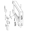
図4には、CWレーザ発振器201、テレセントリックfθレンズ204、ポリゴンミラー203、をそれぞれ3つ用い、1500mm×1800mmの大面積基板に成膜した半導体膜205に対してレーザアニールを行う場合の例を示す。なお図4(A)は上面図、(B)は側面図を示す。
FIG. 4 shows an example in which laser annealing is performed on a
基板に下地膜として酸化膜(SiONやSiO2などの酸化珪素膜)、半導体膜を順次成膜する。半導体膜はCVD法や、スパッタ法等を用い、珪素を主成分とする材料で形成すればよい。本実施の形態では、シランガスを用いたCVD法により非晶質珪素膜を成膜する。成膜方法によっては半導体膜中の水素濃度が高すぎて、レーザアニールに耐えられない場合がある。そこで、レーザアニールに耐える確率を高くするため、半導体膜中の水素濃度を1020/cm3オーダー以下とするとよい。そのため成膜が終了した時点で、水素濃度が上記の値以上である場合は、400〜500℃程度の熱アニールにて、1時間程度の脱水素工程を行うとよい。このように形成された半導体膜に対してレーザアニールを行う。なおレーザアニール前に、半導体膜を所定の形状にパターニングしておいても構わない。 An oxide film (a silicon oxide film such as SiON or SiO 2 ) and a semiconductor film are sequentially formed on the substrate as a base film. The semiconductor film may be formed using a material mainly containing silicon by a CVD method, a sputtering method, or the like. In this embodiment mode, an amorphous silicon film is formed by a CVD method using silane gas. Depending on the film formation method, the hydrogen concentration in the semiconductor film may be too high to withstand laser annealing. Therefore, in order to increase the probability of withstanding laser annealing, the hydrogen concentration in the semiconductor film is preferably set to the order of 10 20 / cm 3 or less. Therefore, when the hydrogen concentration is equal to or higher than the above value when the film formation is completed, it is preferable to perform a dehydrogenation process for about one hour by thermal annealing at about 400 to 500 ° C. Laser annealing is performed on the semiconductor film thus formed. Note that the semiconductor film may be patterned into a predetermined shape before laser annealing.
レーザ発振器201は例えば、LD励起の連続発振型のNd:YVO4レーザの第2高調波(波長532nm)を用いる。出力は10Wとし、TEM00モードのものを使用する。ビームスポット径はφ2.3mm、広がり角は0.35mradとする。
The
なおこの波長は、非晶質珪素膜や基板に対して透光性を示すため、干渉によるレーザアニールの不均一を抑える工夫を施す必要が生じることがある。その場合、例えば、レーザビームの半導体膜205に対する入射角θを0°以外とするとよい。このとき適切な入射角は、ビームスポット形状やサイズに依存する。ビームスポット208の引き伸ばす方向(長軸に相当)は、図4中のY軸方向である。目的によっては他の方向に引き伸ばすこともあるが、本実施例ではスループットを最大とするためY軸方向とする。例えば本実施の形態において、半導体膜205上のビームスポットのサイズを長径400μm、短径20μmの線状の楕円とし、入射面に長径が含まれるように設定すると、適正な入射角θは20°程度である。
In addition, since this wavelength shows translucency with respect to an amorphous silicon film or a substrate, it may be necessary to devise measures for suppressing non-uniformity of laser annealing due to interference. In that case, for example, the incident angle θ of the laser beam with respect to the
光学系202はビームスポット形状を線状に加工するもので、例えば、焦点距離50mmの平凹レンズと、焦点距離200mmの平凸レンズを145mm離して配置し、さらに平凸レンズの後方140mmに、焦点距離250mmの平凸シリンドリカルレンズを配置し、さらに平凸シリンドリカルレンズの後方、145mmに焦点距離100mmの平凹シリンドリカルレンズを配置する。なお、平凸シリンドリカルレンズと平凹シリンドリカルレンズの曲率の方向は同じとする。さらに、平凹シリンドリカルレンズから250mm程度後方にポリゴンミラー203を配置し、テレセントリックfθレンズ204はそれらレンズの仕様に合わせて配置する。テレセントリックfθレンズ204の焦点距離は300mm程度とし、φ120mmとする。
The
以上のような光学系を有するレーザ照射装置において、半導体膜205上で線状に伸ばされたビームスポット208は、ポリゴンミラー203により、速度500mm/sで半導体膜205上を走査する。本発明のポリゴンミラーは、ミラー同士の境界が接していないため、半導体膜上での走査位置を変更する時間がある。
In the laser irradiation apparatus having the optical system as described above, the
そしてポリゴンミラーが有するある一枚のミラーにより、走査できるレーザビームの照射領域の幅を100mmとすると、ポリゴンミラーによりビームスポット208をX軸方向に100mm走査させた後、XYステージ206をY軸方向に200μm(ビームスポットサイズにより決まるレーザビームの走査方向に垂直な結晶の幅)移動させ、再びポリゴンミラー203によりビームスポットを半導体膜205上で走査させる。
If the width of the laser beam irradiation area that can be scanned by one mirror of the polygon mirror is 100 mm, the polygon spot mirror scans the
特に、ポリゴンミラーを用いる場合、ステージの移動距離は、ミラーごとに微調整すると好ましい。これは、ポリゴンミラーは複数のミラーを有し、各ミラーでの反射角度が多少異なることが考えられるためである。このような方法は、実施の形態3で詳細を説明する。このようなレーザ照射において、半導体膜上でレーザビームの照射が照射されない領域は、ポリゴンミラー等の走査手段やレーザビームによって異なり、実施毎に適宜設定すればよい。 In particular, when a polygon mirror is used, it is preferable to finely adjust the moving distance of the stage for each mirror. This is because the polygon mirror has a plurality of mirrors, and the reflection angle at each mirror may be slightly different. Such a method will be described in detail in the third embodiment. In such laser irradiation, the region on the semiconductor film that is not irradiated with the laser beam differs depending on scanning means such as a polygon mirror and the laser beam, and may be set as appropriate for each implementation.
以上を繰り返すことで、図中のA領域をレーザアニールする。A領域はレーザ発振器の数だけできるが、これらの間隔を適宜、例えば100mmずつ開けておく。そして、A領域のアニールが終了後、XYステージ206により、B領域をレーザアニールできる位置まで半導体膜205を移動させ、同様にB領域を一定幅100mmでレーザアニールする。これら一連の動作により、半導体膜205の全面をレーザアニールすることができる。もちろん、半導体膜205全面をレーザアニールする必要はなく、必要な位置のみレーザアニールするとより処理時間を短縮できるので好ましい。この場合、位置決め機構などを精密に作る必要があるが、その構成は実施者が必要な精度を算出し適宜決定するとよい。
By repeating the above, laser annealing is performed on the region A in the figure. The A region can be formed by the number of laser oscillators, but these intervals are appropriately set, for example, by 100 mm. Then, after the annealing of the A region is completed, the
本実施の形態では、レーザビームの半導体膜に入射する角度を一定とするためfθテレセントリックレンズを用いる。これにより、レーザアニールの一様性が得られるが、要求されないときは代わりにfθレンズを用いればよい。また本実施の形態では、間隔を開けて複数のテレセントリックfθレンズ204を配置している。そのため、隣り合うテレセントリックfθレンズが干渉することなく、複数のレーザビームを半導体膜に同時に照射することが可能となる。
In this embodiment, an fθ telecentric lens is used in order to make the angle at which the laser beam is incident on the semiconductor film constant. Thereby, the uniformity of laser annealing can be obtained, but if not required, an fθ lens may be used instead. In the present embodiment, a plurality of telecentric
このように半導体膜の結晶化が行われる。その後、半導体膜を必要に応じて所定の形状にパターニングし、ゲート絶縁膜、ゲート電極、不純物領域を形成し、活性化を行う。本発明のレーザ照射装置及び方法は、半導体膜の活性化にも使用することができる。そして、層間絶縁膜、ソース配線、ドレイン配線、画素電極等を形成し、複数の薄膜トランジスタを有するアクティブマトリクス基板が形成される。またアクティブマトリクス基板を用いて、液晶表示装置、発光装置、その他の表示部を有する表示装置、又は半導体集積回路等を形成することができる。 In this way, the semiconductor film is crystallized. Thereafter, the semiconductor film is patterned into a predetermined shape as necessary to form a gate insulating film, a gate electrode, and an impurity region, and activation is performed. The laser irradiation apparatus and method of the present invention can also be used to activate a semiconductor film. Then, an interlayer insulating film, a source wiring, a drain wiring, a pixel electrode, and the like are formed, and an active matrix substrate having a plurality of thin film transistors is formed. In addition, a liquid crystal display device, a light-emitting device, a display device having another display portion, a semiconductor integrated circuit, or the like can be formed using an active matrix substrate.
以上のように、レーザ発振器を1台のみ用いる場合と比較して高いスループットを得ることができ、特に大型基板に形成される半導体膜のレーザアニールに適す。その結果、薄膜トランジスタの量産性を高めることができる。 As described above, a high throughput can be obtained as compared with the case where only one laser oscillator is used, and it is particularly suitable for laser annealing of a semiconductor film formed on a large substrate. As a result, mass productivity of the thin film transistor can be improved.
なお本実施の形態において、レーザ発振器を複数用いているが、一つのレーザ発振器からのレーザビームをミラー等により分割して、複数のスポットを形成しても構わない。 Although a plurality of laser oscillators are used in this embodiment, a plurality of spots may be formed by dividing a laser beam from one laser oscillator by a mirror or the like.
以上、本実施の形態では走査手段としてポリゴンミラーを用いたが、回転機能を有するガルバノミラーを使用することができる。 As described above, the polygon mirror is used as the scanning means in the present embodiment, but a galvanometer mirror having a rotation function can be used.
(実施の形態3)
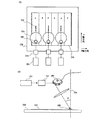
本実施の形態では、ポリゴンミラーとXYステージとの移動タイミングについて、図8を用いて説明する。なお、ポリゴンミラーはN個(1≦n≦N:nは整数)の鏡面体を有するものとする。
(Embodiment 3)
In the present embodiment, the movement timing of the polygon mirror and the XY stage will be described with reference to FIG. The polygon mirror has N mirrors (1 ≦ n ≦ N: n is an integer).
ポリゴンミラーのように複数のミラーを有する走査手段では、ミラー毎に反射角が異なることがある。この状況でXYステージを一定の間隔で移動させると、走査位置の間隔が一定でなくなってしまい均一なレーザ照射ができない。そこで本実施の形態のように、ポリゴンミラーのミラー間、すなわちレーザ照射されないときにXYステージを移動させる距離をミラー毎に設定し、より均一なレーザ照射を行う。 In a scanning unit having a plurality of mirrors such as a polygon mirror, the reflection angle may be different for each mirror. In this situation, if the XY stage is moved at a constant interval, the scanning position interval is not constant, and uniform laser irradiation cannot be performed. Therefore, as in this embodiment, the distance between the mirrors of the polygon mirror, that is, the distance to move the XY stage when laser irradiation is not performed is set for each mirror, and more uniform laser irradiation is performed.
すなわち、図8(A)に示すように、発振器81より射出されたレーザ光82をポリゴンミラー83により走査する光学系において、ポリゴンミラー83は軸85を中心として回転し、ミラー(n)により形成されるスポット(n)、スポット(n+1)、スポット(n+1)、・・・が順次X軸方向の一方方向へ走査され、被照射物84表面にレーザ照射処理が行われる。このとき図8(B)に示すように、ミラー(n)から隣のミラーに移るときのXYステージの移動距離をY(n)で現すと、Y(1)、Y(2)、・・・Y(N)をそれぞれ設定するとより好ましい。なお、Nはミラーの数を示す。 That is, as shown in FIG. 8A, in an optical system that scans laser light 82 emitted from an oscillator 81 with a polygon mirror 83, the polygon mirror 83 rotates about an axis 85 and is formed by a mirror (n). Spot (n), spot (n + 1), spot (n + 1),... Are sequentially scanned in one direction in the X-axis direction, and laser irradiation processing is performed on the surface of the irradiation object 84. At this time, as shown in FIG. 8B, when the movement distance of the XY stage when moving from the mirror (n) to the next mirror is expressed as Y (n), Y (1), Y (2),. -It is more preferable to set Y (N) respectively. N represents the number of mirrors.
XYステージの移動距離Y(n)、Y(n+1)、・・・の設定する方法として、例えば、複数のミラーにそれぞれ番号を付し、一度走査させる。そして、各ミラーの反射角を把握し、これを踏まえてステージの移動距離を決定する。この各移動距離をXYステージの制御装置へ入力すればよい。 As a method for setting the movement distances Y (n), Y (n + 1),... Of the XY stage, for example, a number is assigned to each of a plurality of mirrors, and scanning is performed once. Then, the reflection angle of each mirror is grasped, and the moving distance of the stage is determined based on this. What is necessary is just to input these each movement distance to the control apparatus of XY stage.
このように、ポリゴンミラーのミラー間への移動するときの反射角や距離に合わせてXYステージのX軸方向への移動距離やタイミングを設定すると、より均一なレーザ照射処理を行うことができる。 As described above, when the movement distance and timing in the X-axis direction of the XY stage are set in accordance with the reflection angle and distance when the polygon mirror moves between the mirrors, more uniform laser irradiation processing can be performed.
なお本実施の形態は、ミラーが接して設けられたポリゴンミラーであっても、適応することができる。すなわち接して設けられたミラーの境界位置で、XYステージを移動させるとき、XYステージの移動距離を調整し、均一なレーザ照射が可能となる。またY軸方向へのステージの移動時間を設けたいときはレーザビームの走査の両端又は片端(一端又は他端)を遮光する手段を設けても構わない。 This embodiment can be applied even to a polygon mirror provided in contact with a mirror. That is, when the XY stage is moved at the boundary position of the mirrors provided in contact with each other, the movement distance of the XY stage is adjusted, and uniform laser irradiation becomes possible. Further, when it is desired to provide the stage moving time in the Y-axis direction, means for shielding light at both ends or one end (one end or the other end) of the laser beam scanning may be provided.
(実施の形態4)
本実施の形態では、アクティブマトリクス基板を用いて作製される発光装置について、図5を用いて説明する。
(Embodiment 4)
In this embodiment, a light-emitting device manufactured using an active matrix substrate will be described with reference to FIGS.
図5(A)には、発光装置、具体的にはELモジュールの断面を示す。また図5(B)には、ELモジュールの発光素子(有機化合物層(EL層ともいう)、第1の導電膜及び第2の導電膜を有する)の積層構造を拡大したものを示す。 FIG. 5A shows a cross section of a light-emitting device, specifically, an EL module. FIG. 5B shows an enlarged view of a stacked structure of light-emitting elements of an EL module (having an organic compound layer (also referred to as an EL layer), a first conductive film, and a second conductive film).
図5(A)は、第1の基板400、下地絶縁膜401、本発明のレーザ照射装置を用いてレーザアニールされて形成されるTFT422、第1の導電膜(電極)403、絶縁物(隔壁、障壁、土手、バンクとも呼ばれる)404、有機化合物層405、第2の導電膜(電極)406、保護膜407、空隙408、第2の基板409を示す。
FIG. 5A shows a first substrate 400, a base insulating film 401, a
第1の基板及び第2の基板としては、ガラス基板、石英基板やシリコン基板、プラスチック基板、金属基板、ステンレス基板、可撓性基板などを用いることができる。可撓性基板とは、PET、PES、PEN、アクリルなどからなるフィルム状の基板のことであり、可撓性基板を用いて発光装置を作製すれば、軽量化が見込まれる。可撓性基板の表面、または表面および裏面にアルミ膜(AlON、AlN、AlOなど)、炭素膜(DLCなど)、SiNなどのバリア層を単層または多層にして形成すれば、耐久性やガスバリア性などが向上するので望ましい。 As the first substrate and the second substrate, a glass substrate, a quartz substrate, a silicon substrate, a plastic substrate, a metal substrate, a stainless steel substrate, a flexible substrate, or the like can be used. A flexible substrate is a film-like substrate made of PET, PES, PEN, acrylic, or the like. If a light-emitting device is manufactured using a flexible substrate, weight reduction is expected. If a barrier layer such as an aluminum film (AlON, AlN, AlO, etc.), a carbon film (DLC, etc.), SiN or the like is formed on the surface of the flexible substrate or on the front and back surfaces, the durability and gas barrier This is desirable because of improved properties.
なお有機化合物層からの発光が上方又は下方のいずれかに出射されるかにより、第1の導電膜及び第2の導電膜のいずれかを透光性をする導電膜、例えばITO等から形成する。また両方に出射する場合は、第1の導電膜及び第2の導電膜を透光性を有する導電膜として形成する。 Depending on whether light emitted from the organic compound layer is emitted upward or downward, either the first conductive film or the second conductive film is formed from a light-transmitting conductive film, such as ITO. . In the case of emitting light to both, the first conductive film and the second conductive film are formed as light-transmitting conductive films.
第1の基板400上に設けられたTFT422(本実施の形態では、pチャネル型TFT)は、有機化合物層405に流れる電流を制御する素子であり、ドレイン領域(極性によってはソース領域)として機能する不純物領域411と、チャネル形成領域412と、チャネル形成領域上に設けられたゲート電極417を有する。また、第1の導電膜403と、不純物領域411とを電気的に接続するためのドレイン領域(またはソース領域)に接続されるドレイン電極(またはソース電極)416を有する。また、ドレイン電極416と同じ工程で電源供給線やソース配線などの配線418を同時に形成することができる。
A TFT 422 (a p-channel TFT in this embodiment mode) provided over the first substrate 400 is an element that controls current flowing in the
第1の基板400上には下地絶縁膜(ここでは、下層を窒化絶縁膜、上層を酸化絶縁膜)401形成されており、ゲート電極417と半導体膜との間には、ゲート絶縁膜が設けられている。また、層間絶縁膜402は有機材料または無機材料を有するように形成される。ここでは図示しないが、一つの画素には、他にもTFT(nチャネル型TFTまたはpチャネル型TFT)を一つ、または複数設けている。また、一つのチャネル形成領域412を有するTFTを示したが、特に限定されず、複数のチャネルを有する、所謂マルチチャネル型TFTとしてもよい。
A base insulating film (here, a nitride insulating film as a lower layer and an oxide insulating film as an upper layer) 401 is formed over the first substrate 400, and a gate insulating film is provided between the
加えて、ここではトップゲート型TFTを例として説明したが、TFT構造に関係なく本発明を適用することが可能であり、例えばボトムゲート型(逆スタガ型)TFTや順スタガ型TFTに適用することが可能である。 In addition, the top gate type TFT has been described as an example here, but the present invention can be applied regardless of the TFT structure, and is applied to, for example, a bottom gate type (reverse stagger type) TFT or a forward stagger type TFT. It is possible.
また、第1の導電膜403は、発光素子の陽極(或いは陰極)となる。第1の導電膜において、透明導電膜を用いる場合、ITO(酸化インジウム酸化スズ合金)、酸化インジウム酸化亜鉛合金(In2O3―ZnO)、酸化亜鉛(ZnO)等を用いることができる。 In addition, the first conductive film 403 serves as an anode (or a cathode) of the light emitting element. In the first conductive film, when using a transparent conductive film, ITO (indium tin oxide alloy), indium oxide-zinc oxide alloy (In 2 O 3 -ZnO), it can be used zinc oxide (ZnO) and the like.
また、第1の導電膜403の端部(および配線418)を覆う絶縁物404(バンク、隔壁、障壁、土手などと呼ばれる)を有している。絶縁物404としては、無機材料(酸化シリコン、窒化シリコン、酸化窒化シリコンなど)、感光性または非感光性の有機材料(ポリイミド、アクリル、ポリアミド、ポリイミドアミド、レジストまたはベンゾシクロブテン)、またはこれらの積層などを用いることができる。なお本実施の形態では、窒化シリコン膜で覆われた感光性の有機樹脂を用いる。例えば、有機樹脂の材料としてポジ型の感光性アクリルを用いた場合、絶縁物の上端部のみに曲率半径を有する曲面を持たせることが好ましい。また、絶縁物として、感光性の光によってエッチャントに不溶解性となるネガ型、或いは光によってエッチャントに溶解性となるポジ型のいずれも使用することができる。 In addition, an insulator 404 (referred to as a bank, a partition, a barrier, a bank, or the like) is provided to cover an end portion (and the wiring 418) of the first conductive film 403. As the insulator 404, an inorganic material (silicon oxide, silicon nitride, silicon oxynitride, or the like), a photosensitive or non-photosensitive organic material (polyimide, acrylic, polyamide, polyimide amide, resist, or benzocyclobutene), or a material thereof Lamination etc. can be used. Note that in this embodiment mode, a photosensitive organic resin covered with a silicon nitride film is used. For example, when positive photosensitive acrylic is used as the organic resin material, it is preferable that only the upper end portion of the insulator has a curved surface having a curvature radius. As the insulator, either a negative type that becomes insoluble in an etchant by photosensitive light or a positive type that becomes soluble in an etchant by light can be used.
また、有機化合物層405は、蒸着法、インクジェット法または塗布法を用いて形成する。本実施の形態では、有機化合物層を蒸着装置で成膜を行い、均一な膜厚を得る。例えば、蒸着法を用いる場合、真空度が5×10⁻³Torr(0.665Pa)以下、好ましくは10-4〜10-6Paまで真空排気された成膜室で蒸着を行う。蒸着の際、予め、加熱により有機化合物は気化されており、蒸着時にシャッターが開くことにより基板の方向へ飛散する。気化された有機化合物は、上方に飛散し、メタルマスクに設けられた開口部を通って蒸着される。なお、信頼性を向上させるため、有機化合物層405の形成直前に真空加熱(100℃〜250℃)を行って脱気を行うことが好ましい。
The
なお図5(B)に示すように、有機化合物層405は、陽極側から順に、HIL(ホール注入層)、HTL(ホール輸送層)、EML(発光層)、ETL(電子輸送層)、EIL(電子注入層)の順に積層されている。代表的には、HILとしてCuPc、HTLとしてα−NPD、ETLとしてBCP、EILとしてBCP:Liをそれぞれ用いる。なお、有機化合物は、無機材料を有したり、有機材料と、無機材料との混合材料を有してもよい。
As shown in FIG. 5B, the
また、有機化合物層405として、フルカラー表示とする場合、赤色(R)、緑色(G)、青色(B)の発光を示す材料を、それぞれ蒸着マスクを用いた蒸着法、またはインクジェット法などによって適宜、選択的に形成することができる。具体的には、HILとしてCuPcやPEDOT、HTLとしてα−NPD、ETLとしてBCPやAlq3、EILとしてBCP:LiやCaF2をそれぞれ用いる。また例えばEMLは、R、G、Bのそれぞれの発光色に対応したドーパント(Rの場合DCM等、Gの場合DMQD等)をドープしたAlq3を用いればよい。なお、上記有機化合物層は、積層構造に限定されず、単層構造であってもよい。
In the case of full-color display as the
より具体的な有機化合物層の積層構造は、赤色の発光を示す有機化合物層405を形成する場合、例えば、CuPcを30nm形成し、α-NPDを60nm形成した後、同一のマスクを用いて、赤色の発光層としてDCM2及びルブレンが添加されたAlq3を40nm形成し、電子輸送層としてBCPを40nm形成し、電子注入層としてLiが添加されたBCPを1nm形成する。また、緑色の発光を示す有機化合物層を形成する場合、例えば、CuPcを30nm形成し、α―NPDを60nm成膜した後、同一の蒸着マスクを用いて、緑色の発光層としてクマリン545Tが添加されたAlq3を40nm形成し、電子輸送層としてBCPを40nm形成し、電子注入層としてLiが添加されたBCPを1nm形成する。また、青色の発光を示す有機化合物を含む層を形成する場合、例えば、CuPcを30nm形成し、α-NPDを60nm形成した後、同一のマスクを用いて発光層としてビス[2−(2−ヒドロキシフェニル)ベンゾオキサゾラト]亜鉛:Zn(PBO)2を10nm形成し、電子輸送層としてBCPを40nm成膜し、電子注入層としてLiが添加されたBCPを1nm形成する。以上、各色の有機化合物層のうち、共通しているCuPcやα-NPDは、画素部全面に形成することができる。またマスクは、各色で共有することもでき、例えば、赤色の有機化合物層を形成後、マスクをずらして、緑色の有機化合物層、再度マスクをずらして青色の有機化合物層を形成することができる。なお、形成する各色の有機化合物層の順序は適宜設定すればよい。
More specifically, in the case of forming the
また白色発光の場合、カラーフィルターや色変換層などを別途設けることによってフルカラー表示を行ってもよい。上方に発光する白色光に対するカラーフィルターや色変換層は、第2の基板に設けた後、第1の基板へ張り合わせればよい。また、下方に発光する白色光に対するカラーフィルターや色変換層は、ドレイン電極(またはソース電極)416を形成後、絶縁膜を介して形成することができる。その後、カラーフィルターや色変換層上に絶縁膜、第2の導電膜の順に形成するため、ドレイン電極(またはソース電極)416と第2の導電膜とは、絶縁膜に形成されるコンタクトを介して接続すればよい。 In the case of white light emission, full color display may be performed by separately providing a color filter, a color conversion layer, or the like. A color filter or a color conversion layer for white light emitted upward may be provided on the second substrate and then attached to the first substrate. Further, a color filter and a color conversion layer for white light emitted downward can be formed through an insulating film after the drain electrode (or source electrode) 416 is formed. After that, since the insulating film and the second conductive film are formed in this order on the color filter and the color conversion layer, the drain electrode (or source electrode) 416 and the second conductive film are connected via a contact formed in the insulating film. And connect.
本発明のガルバノミラーやポリゴンミラーにより、均一性の高い結晶性半導体膜を有する発光装置を提供することができる。その結果、表示部のレーザビームの照射ムラ(表示ムラとなる)の低減された発光装置を提供することができる。 With the galvanometer mirror or polygon mirror of the present invention, a light-emitting device having a highly uniform crystalline semiconductor film can be provided. As a result, it is possible to provide a light-emitting device in which irradiation unevenness of the laser beam on the display portion (which causes display unevenness) is reduced.
なお、本発明のアクティブマトリクス基板は発光装置以外の液晶表示装置やその他の表示装置、更には半導体集積回路やCPUにも採用することができる。 Note that the active matrix substrate of the present invention can also be used in liquid crystal display devices other than light-emitting devices, other display devices, semiconductor integrated circuits, and CPUs.
(実施の形態5)
本発明により作製されたアクティブマトリクス基板は、様々な電子機器に適用することができる。電子機器としては、携帯情報端末(携帯電話機、モバイルコンピュータ、携帯型ゲーム機又は電子書籍等)、ビデオカメラ、デジタルカメラ、ゴーグル型ディスプレイ、表示ディスプレイ、ナビゲーションシステム等が挙げられる。これら電子機器の具体例を図6に示す。
(Embodiment 5)
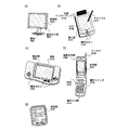
The active matrix substrate manufactured according to the present invention can be applied to various electronic devices. Examples of the electronic device include a portable information terminal (a mobile phone, a mobile computer, a portable game machine, an electronic book, etc.), a video camera, a digital camera, a goggle type display, a display display, a navigation system, and the like. Specific examples of these electronic devices are shown in FIGS.
図6(A)はディスプレイであり、筐体4001、音声出力部4002、表示部4003等を含む。本発明により形成されたアクティブマトリクス基板により発光素子又は液晶材料を有する表示部4003を完成することができる。表示装置は、パソコン用、TV放送受信用、広告表示用など全ての情報表示装置が含まれる。
FIG. 6A illustrates a display, which includes a
図6(B)はモバイルコンピュータであり、本体4101、スタイラス4102、表示部4103、操作ボタン4104、外部インターフェイス4105等を含む。本発明により形成されたアクティブマトリクス基板により発光素子や液晶材料を有する表示部4103を完成することができる。
FIG. 6B illustrates a mobile computer, which includes a
図6(C)はゲーム機であり、本体4201、表示部4202、操作ボタン4203等を含む。本発明により形成されたアクティブマトリクス基板により発光素子や液晶材料を有する表示部4202を完成することができる。図6(D)は携帯電話機であり、本体4301、音声出力部4302、音声入力部4303、表示部4304、操作スイッチ4305、アンテナ4306等を含む。本発明により形成されたアクティブマトリクス基板により発光素子や液晶材料を有する表示部4304を完成することができる。
FIG. 6C illustrates a game machine, which includes a
図6(E)は電子ブックリーダーであり、表示部4401等を含む。本発明により形成されたアクティブマトリクス基板により発光素子や液晶材料を有する表示部4202を完成することができる。
FIG. 6E illustrates an electronic book reader that includes a
以上のように、本発明の適用範囲は極めて広く、あらゆる分野の電子機器に用いることが可能である。特に、アクティブマトリクス基板の絶縁基板をフレキシブル基板とすることで薄型や軽量が実現することができる。 As described above, the applicable range of the present invention is so wide that the present invention can be used for electronic devices in various fields. In particular, thin and light weight can be realized by using a flexible substrate as the insulating substrate of the active matrix substrate.
(実施の形態6)
なお本発明に用いられるビームは、CWビームに限定されず、パルス的に出力されるエネルギービーム(パルスビーム、特に、光源にレーザを使用する場合パルスレーザと表記する)を用いることができる。
(Embodiment 6)
Note that the beam used in the present invention is not limited to a CW beam, and an energy beam (pulse beam, particularly expressed as a pulse laser when a laser is used as a light source) can be used.
本発明のパルスレーザは、半導体膜がレーザ光によって溶融してから固化するまでに、次のレーザ光を照射できるような発振周波数でレーザ光を発振させることで、走査方向に向かって連続的に成長した結晶粒を得ることができるように制御する。すなわち、パルス発振の周期(発振周波数)が、半導体膜が溶融してから完全に固化するまでの時間よりも短くなるように、発振周波数の下限を定めたパルスビームを使用することができる。 The pulse laser of the present invention continuously oscillates in the scanning direction by oscillating the laser beam at an oscillation frequency that can be irradiated with the next laser beam after the semiconductor film is melted and solidified by the laser beam. Control is performed so that grown crystal grains can be obtained. That is, it is possible to use a pulse beam in which the lower limit of the oscillation frequency is set so that the pulse oscillation period (oscillation frequency) is shorter than the time from when the semiconductor film is melted until it is completely solidified.
例えば光源にレーザを用いたパルスレーザにおいて、具体的な発振周波数は10MHz以上とし、通常用いられている数十Hz〜数百Hzの周波数よりも著しく高い周波数帯を使用する。 For example, in a pulse laser using a laser as a light source, a specific oscillation frequency is set to 10 MHz or more, and a frequency band significantly higher than a frequency of several tens to several hundreds Hz that is normally used is used.
レーザ光を半導体膜に照射してから半導体膜が完全に固化するまでの時間は数十nsec〜数百nsecと言われている。このように高い周波数を使用することによって、半導体膜がレーザ光によって溶融してから固化するまでに、次のパルスのレーザ光を照射することができる。したがって、従来のパルスレーザを用いる場合と異なり、半導体膜中において固液界面を連続的に移動させることができるので、走査方向に向かって連続的に成長した結晶粒を有する半導体膜が形成される。具体的には、結晶粒の走査方向における幅が10〜30μm、走査方向に対して垂直な方向における幅が1〜5μm程度の結晶粒の集合を形成することができ、CWレーザと同程度の結晶粒を得ることができるからである。そして該走査方向に沿って長く伸びた単結晶の結晶粒を形成することで、少なくともTFTのキャリアの移動方向には結晶粒界のほとんど存在しない半導体膜の形成が可能となる。 It is said that the time from when the semiconductor film is irradiated with laser light until the semiconductor film is completely solidified is several tens to several hundreds nsec. By using such a high frequency, it is possible to irradiate the next pulse of laser light before the semiconductor film is melted by the laser light and solidified. Therefore, unlike the case of using a conventional pulse laser, the solid-liquid interface can be continuously moved in the semiconductor film, so that a semiconductor film having crystal grains continuously grown in the scanning direction is formed. . Specifically, a set of crystal grains having a width of 10 to 30 μm in the scanning direction of crystal grains and a width of about 1 to 5 μm in a direction perpendicular to the scanning direction can be formed. This is because crystal grains can be obtained. By forming single crystal crystal grains extending long along the scanning direction, it is possible to form a semiconductor film having almost no crystal grain boundaries in at least the TFT carrier movement direction.
上記周波数での発振が可能であるならば、パルスビームとしてArレーザ、Krレーザ、エキシマレーザ、CO2レーザ、YAGレーザ、Y2O3レーザ、YVO4レーザ、YLFレーザ、YAlO3レーザ、ガラスレーザ、ルビーレーザ、アレキサンドライトレーザ、Ti:サファイヤレーザ、銅蒸気レーザまたは金蒸気レーザから射出されるビームを用いることができる。 If oscillation at the above-mentioned frequency is possible, an Ar laser, a Kr laser, an excimer laser, a CO 2 laser, a YAG laser, a Y 2 O 3 laser, a YVO 4 laser, a YLF laser, a YAlO 3 laser, a glass laser can be used as a pulse beam. A beam emitted from a ruby laser, an alexandrite laser, a Ti: sapphire laser, a copper vapor laser, or a gold vapor laser can be used.
例えば、エネルギー2W、TEM(00)の発振モード、第2高調波(532nm)、発振周波数80MHz、パルス幅12psecのYVO4レーザを用いることができ、このレーザ光を発振するパルスレーザ照射装置を用いることができる。なお、レーザ光を光学系により加工することで半導体膜の表面に形成されるスポットは、短軸10μm、長軸100μmの矩形状となる。発振周波数を80MHzとすることで、固液界面を連続的に移動させることができるので、走査方向に向かって連続的に成長した結晶粒が形成される。該走査方向に沿って長く延びた単結晶の粒を形成することで、少なくともTFTのチャネル方向には結晶粒界のほとんど存在しない半導体膜の形成が可能となる。 For example, a YVO 4 laser having an energy of 2 W, an oscillation mode of TEM (00), a second harmonic (532 nm), an oscillation frequency of 80 MHz, and a pulse width of 12 psec can be used, and a pulse laser irradiation apparatus that oscillates this laser beam is used. be able to. Note that spots formed on the surface of the semiconductor film by processing laser light with an optical system have a rectangular shape with a short axis of 10 μm and a long axis of 100 μm. Since the solid-liquid interface can be continuously moved by setting the oscillation frequency to 80 MHz, crystal grains that are continuously grown in the scanning direction are formed. By forming single crystal grains extending in the scanning direction, it is possible to form a semiconductor film having few crystal grain boundaries at least in the channel direction of the TFT.
すなわち、連続的又はパルス的に発振されるレーザビームのいずれを用いる場合であっても、本発明のガルバノミラーやポリゴンミラーにより、均一なレーザ照射を行うことができる。 That is, even when using either a continuous or pulsed laser beam, uniform laser irradiation can be performed by the galvanometer mirror or polygon mirror of the present invention.
Claims (5)
レーザビームの光軸上に配置されるよう軸に固定され、前記軸を中心として一方向に一定速度で回転するガルバノミラーと、
被照射物へレーザビームが照射されないときにビームスポットの走査位置を変更するステージと、を有することを特徴とするレーザビーム照射装置。 An oscillator that outputs a continuous oscillation or a laser beam with an oscillation frequency of 10 MHz or more;
A galvanometer mirror fixed to an axis so as to be disposed on the optical axis of the laser beam, and rotating at a constant speed in one direction around the axis ;
And a stage for changing the scanning position of the beam spot when the irradiation object is not irradiated with the laser beam.
前記発振器及び前記ガルバノミラーを複数有することを特徴とするレーザビーム照射装置。 In claim 1,
A laser beam irradiation apparatus comprising a plurality of the oscillator and the galvanometer mirror .
レーザビームの光軸上に配置されるよう軸に固定され、前記軸を中心として一方向に一定速度で回転し、ミラー同士を接して配置しないポリゴンミラーと、A polygon mirror that is fixed to an axis so as to be arranged on the optical axis of the laser beam, rotates at a constant speed in one direction around the axis, and does not arrange the mirrors in contact with each other;
被照射物へレーザビームが照射されないときに、前記ポリゴンミラーが有するミラー毎に反射するレーザビームの入射角による照射位置のずれを補正してビームスポットの走査位置を変更するステージと、を有することを特徴とするレーザビーム照射装置。A stage for correcting a beam spot scanning position by correcting a deviation of an irradiation position due to an incident angle of a laser beam reflected by each mirror of the polygon mirror when the irradiation object is not irradiated with a laser beam. A laser beam irradiation apparatus characterized by the above.
前記発振器及び前記ポリゴンミラーを複数有することを特徴とするレーザビーム照射装置。A laser beam irradiation apparatus comprising a plurality of the oscillator and the polygon mirror.
請求項1乃至請求項4のいずれか一に記載のレーザビーム照射装置を用いて、前記半導体膜に対してレーザビームを照射する工程を有することを特徴とする薄膜トランジスタの作製方法。A method for manufacturing a thin film transistor, comprising: a step of irradiating the semiconductor film with a laser beam using the laser beam irradiation apparatus according to claim 1.
Priority Applications (1)
| Application Number | Priority Date | Filing Date | Title |
|---|---|---|---|
| JP2004123375A JP4515136B2 (en) | 2003-04-21 | 2004-04-19 | Laser beam irradiation apparatus and method for manufacturing thin film transistor |
Applications Claiming Priority (2)
| Application Number | Priority Date | Filing Date | Title |
|---|---|---|---|
| JP2003116408 | 2003-04-21 | ||
| JP2004123375A JP4515136B2 (en) | 2003-04-21 | 2004-04-19 | Laser beam irradiation apparatus and method for manufacturing thin film transistor |
Publications (3)
| Publication Number | Publication Date |
|---|---|
| JP2004343091A JP2004343091A (en) | 2004-12-02 |
| JP2004343091A5 JP2004343091A5 (en) | 2007-05-31 |
| JP4515136B2 true JP4515136B2 (en) | 2010-07-28 |
Family
ID=33543090
Family Applications (1)
| Application Number | Title | Priority Date | Filing Date |
|---|---|---|---|
| JP2004123375A Expired - Fee Related JP4515136B2 (en) | 2003-04-21 | 2004-04-19 | Laser beam irradiation apparatus and method for manufacturing thin film transistor |
Country Status (1)
| Country | Link |
|---|---|
| JP (1) | JP4515136B2 (en) |
Families Citing this family (7)
| Publication number | Priority date | Publication date | Assignee | Title |
|---|---|---|---|---|
| KR101287314B1 (en) | 2005-12-05 | 2013-07-17 | 더 트러스티이스 오브 콜롬비아 유니버시티 인 더 시티 오브 뉴욕 | Systems and methods for processing a film, and thin films |
| FI20060177L (en) * | 2006-02-23 | 2007-08-24 | Picodeon Ltd Oy | The method produces good quality surfaces and a product with a good quality surface |
| KR101398379B1 (en) * | 2006-02-23 | 2014-05-22 | 피코데온 리미티드 오와이 | Semiconductor and an arrangement and a method for producing a semiconductor |
| FI20060178L (en) * | 2006-02-23 | 2007-08-24 | Picodeon Ltd Oy | Surface coating procedure |
| WO2007096484A2 (en) * | 2006-02-23 | 2007-08-30 | Picodeon Ltd Oy | Coating with carbon nitride and carbon nitride coated product |
| US8553311B2 (en) | 2010-04-02 | 2013-10-08 | Electro Scientific Industries, Inc. | Method for accomplishing high-speed intensity variation of a polarized output laser beam |
| JP2023009330A (en) * | 2021-07-07 | 2023-01-20 | 川崎重工業株式会社 | Laser welding method |
Citations (3)
| Publication number | Priority date | Publication date | Assignee | Title |
|---|---|---|---|---|
| JP2002231628A (en) * | 2001-02-01 | 2002-08-16 | Sony Corp | Method of forming semiconductor thin film, method of manufacturing semiconductor device, device used for carrying out the same, and electro-optical device |
| JP2003045820A (en) * | 2001-07-30 | 2003-02-14 | Semiconductor Energy Lab Co Ltd | Laser irradiation apparatus, and method, and method of manufacturing semiconductor device |
| JP2003059859A (en) * | 2001-08-10 | 2003-02-28 | Semiconductor Energy Lab Co Ltd | Device and method for irradiating laser and method for manufacturing semiconductor device |
Family Cites Families (2)
| Publication number | Priority date | Publication date | Assignee | Title |
|---|---|---|---|---|
| JPH1032166A (en) * | 1996-07-16 | 1998-02-03 | Toyota Motor Corp | Formation of crystal thin film using laser ablation method |
| JPH11342485A (en) * | 1998-05-29 | 1999-12-14 | Nec Corp | Laser processing machine, and method for forming processing hole for through hole and blind via hole |
-
2004
- 2004-04-19 JP JP2004123375A patent/JP4515136B2/en not_active Expired - Fee Related
Patent Citations (3)
| Publication number | Priority date | Publication date | Assignee | Title |
|---|---|---|---|---|
| JP2002231628A (en) * | 2001-02-01 | 2002-08-16 | Sony Corp | Method of forming semiconductor thin film, method of manufacturing semiconductor device, device used for carrying out the same, and electro-optical device |
| JP2003045820A (en) * | 2001-07-30 | 2003-02-14 | Semiconductor Energy Lab Co Ltd | Laser irradiation apparatus, and method, and method of manufacturing semiconductor device |
| JP2003059859A (en) * | 2001-08-10 | 2003-02-28 | Semiconductor Energy Lab Co Ltd | Device and method for irradiating laser and method for manufacturing semiconductor device |
Also Published As
| Publication number | Publication date |
|---|---|
| JP2004343091A (en) | 2004-12-02 |
Similar Documents
| Publication | Publication Date | Title |
|---|---|---|
| US7746528B2 (en) | Beam irradiation apparatus, beam irradiation method, and method for manufacturing thin film transistor | |
| US7915099B2 (en) | Beam irradiation apparatus, beam irradiation method, and method for manufacturing semiconductor device | |
| US7247527B2 (en) | Method for manufacturing semiconductor device, and laser irradiation apparatus | |
| US6392810B1 (en) | Laser irradiation apparatus, laser irradiation method, beam homogenizer, semiconductor device, and method of manufacturing the semiconductor device | |
| JP5063660B2 (en) | Method for manufacturing semiconductor device | |
| US6770546B2 (en) | Method of manufacturing semiconductor device | |
| US7476629B2 (en) | Beam irradiation apparatus, beam irradiation method, and method for manufacturing thin film transistor | |
| JP2004179389A (en) | Laser irradiating device and method, and method for manufacturing semiconductor device | |
| JP2004179389A6 (en) | Laser irradiation apparatus, laser irradiation method, and manufacturing method of semiconductor device | |
| KR20090068196A (en) | Laser irradiating device and manufacturing method of semiconductor device | |
| KR101065660B1 (en) | Laser irradiation method, laser irradiation apparatus, and method for manufacturing semiconductor device | |
| JP2003045820A (en) | Laser irradiation apparatus, and method, and method of manufacturing semiconductor device | |
| US7348222B2 (en) | Method for manufacturing a thin film transistor and method for manufacturing a semiconductor device | |
| US20050006655A1 (en) | Laser beam treatment device and semiconductor device | |
| JP4515136B2 (en) | Laser beam irradiation apparatus and method for manufacturing thin film transistor | |
| JP4566503B2 (en) | Laser processing apparatus and semiconductor device manufacturing method | |
| JP4503344B2 (en) | Beam irradiation apparatus and method for manufacturing semiconductor device | |
| JP4503343B2 (en) | Beam irradiation apparatus, beam irradiation method, and method for manufacturing thin film transistor | |
| JP2003158086A (en) | Laser processor | |
| JP4741204B2 (en) | Method for manufacturing semiconductor device | |
| JP2007129257A (en) | Laser irradiation device, laser irradiation method, method of fabricating semiconductor device |
Legal Events
| Date | Code | Title | Description |
|---|---|---|---|
| A521 | Written amendment |
Free format text: JAPANESE INTERMEDIATE CODE: A523 Effective date: 20070409 |
|
| A621 | Written request for application examination |
Free format text: JAPANESE INTERMEDIATE CODE: A621 Effective date: 20070409 |
|
| A977 | Report on retrieval |
Free format text: JAPANESE INTERMEDIATE CODE: A971007 Effective date: 20081202 |
|
| A131 | Notification of reasons for refusal |
Free format text: JAPANESE INTERMEDIATE CODE: A131 Effective date: 20100216 |
|
| A521 | Written amendment |
Free format text: JAPANESE INTERMEDIATE CODE: A523 Effective date: 20100401 |
|
| TRDD | Decision of grant or rejection written | ||
| A01 | Written decision to grant a patent or to grant a registration (utility model) |
Free format text: JAPANESE INTERMEDIATE CODE: A01 Effective date: 20100511 |
|
| A01 | Written decision to grant a patent or to grant a registration (utility model) |
Free format text: JAPANESE INTERMEDIATE CODE: A01 |
|
| A61 | First payment of annual fees (during grant procedure) |
Free format text: JAPANESE INTERMEDIATE CODE: A61 Effective date: 20100512 |
|
| R150 | Certificate of patent or registration of utility model |
Free format text: JAPANESE INTERMEDIATE CODE: R150 |
|
| FPAY | Renewal fee payment (event date is renewal date of database) |
Free format text: PAYMENT UNTIL: 20130521 Year of fee payment: 3 |
|
| FPAY | Renewal fee payment (event date is renewal date of database) |
Free format text: PAYMENT UNTIL: 20130521 Year of fee payment: 3 |
|
| FPAY | Renewal fee payment (event date is renewal date of database) |
Free format text: PAYMENT UNTIL: 20130521 Year of fee payment: 3 |
|
| FPAY | Renewal fee payment (event date is renewal date of database) |
Free format text: PAYMENT UNTIL: 20140521 Year of fee payment: 4 |
|
| R250 | Receipt of annual fees |
Free format text: JAPANESE INTERMEDIATE CODE: R250 |
|
| R250 | Receipt of annual fees |
Free format text: JAPANESE INTERMEDIATE CODE: R250 |
|
| R250 | Receipt of annual fees |
Free format text: JAPANESE INTERMEDIATE CODE: R250 |
|
| R250 | Receipt of annual fees |
Free format text: JAPANESE INTERMEDIATE CODE: R250 |
|
| LAPS | Cancellation because of no payment of annual fees |