JP4514376B2 - Nitride semiconductor laser device - Google Patents
Nitride semiconductor laser device Download PDFInfo
- Publication number
- JP4514376B2 JP4514376B2 JP2001295939A JP2001295939A JP4514376B2 JP 4514376 B2 JP4514376 B2 JP 4514376B2 JP 2001295939 A JP2001295939 A JP 2001295939A JP 2001295939 A JP2001295939 A JP 2001295939A JP 4514376 B2 JP4514376 B2 JP 4514376B2
- Authority
- JP
- Japan
- Prior art keywords
- nitride semiconductor
- semiconductor laser
- laser device
- support base
- thickness
- Prior art date
- Legal status (The legal status is an assumption and is not a legal conclusion. Google has not performed a legal analysis and makes no representation as to the accuracy of the status listed.)
- Expired - Fee Related
Links
Images


Classifications
-
- H—ELECTRICITY
- H01—ELECTRIC ELEMENTS
- H01S—DEVICES USING THE PROCESS OF LIGHT AMPLIFICATION BY STIMULATED EMISSION OF RADIATION [LASER] TO AMPLIFY OR GENERATE LIGHT; DEVICES USING STIMULATED EMISSION OF ELECTROMAGNETIC RADIATION IN WAVE RANGES OTHER THAN OPTICAL
- H01S5/00—Semiconductor lasers
- H01S5/02—Structural details or components not essential to laser action
- H01S5/022—Mountings; Housings
- H01S5/0235—Method for mounting laser chips
- H01S5/02355—Fixing laser chips on mounts
- H01S5/0237—Fixing laser chips on mounts by soldering
-
- B—PERFORMING OPERATIONS; TRANSPORTING
- B82—NANOTECHNOLOGY
- B82Y—SPECIFIC USES OR APPLICATIONS OF NANOSTRUCTURES; MEASUREMENT OR ANALYSIS OF NANOSTRUCTURES; MANUFACTURE OR TREATMENT OF NANOSTRUCTURES
- B82Y20/00—Nanooptics, e.g. quantum optics or photonic crystals
-
- H—ELECTRICITY
- H01—ELECTRIC ELEMENTS
- H01L—SEMICONDUCTOR DEVICES NOT COVERED BY CLASS H10
- H01L24/00—Arrangements for connecting or disconnecting semiconductor or solid-state bodies; Methods or apparatus related thereto
- H01L24/01—Means for bonding being attached to, or being formed on, the surface to be connected, e.g. chip-to-package, die-attach, "first-level" interconnects; Manufacturing methods related thereto
- H01L24/02—Bonding areas ; Manufacturing methods related thereto
- H01L24/04—Structure, shape, material or disposition of the bonding areas prior to the connecting process
- H01L24/05—Structure, shape, material or disposition of the bonding areas prior to the connecting process of an individual bonding area
-
- H—ELECTRICITY
- H01—ELECTRIC ELEMENTS
- H01S—DEVICES USING THE PROCESS OF LIGHT AMPLIFICATION BY STIMULATED EMISSION OF RADIATION [LASER] TO AMPLIFY OR GENERATE LIGHT; DEVICES USING STIMULATED EMISSION OF ELECTROMAGNETIC RADIATION IN WAVE RANGES OTHER THAN OPTICAL
- H01S5/00—Semiconductor lasers
- H01S5/30—Structure or shape of the active region; Materials used for the active region
- H01S5/34—Structure or shape of the active region; Materials used for the active region comprising quantum well or superlattice structures, e.g. single quantum well [SQW] lasers, multiple quantum well [MQW] lasers or graded index separate confinement heterostructure [GRINSCH] lasers
- H01S5/343—Structure or shape of the active region; Materials used for the active region comprising quantum well or superlattice structures, e.g. single quantum well [SQW] lasers, multiple quantum well [MQW] lasers or graded index separate confinement heterostructure [GRINSCH] lasers in AIIIBV compounds, e.g. AlGaAs-laser, InP-based laser
- H01S5/34333—Structure or shape of the active region; Materials used for the active region comprising quantum well or superlattice structures, e.g. single quantum well [SQW] lasers, multiple quantum well [MQW] lasers or graded index separate confinement heterostructure [GRINSCH] lasers in AIIIBV compounds, e.g. AlGaAs-laser, InP-based laser with a well layer based on Ga(In)N or Ga(In)P, e.g. blue laser
-
- H—ELECTRICITY
- H01—ELECTRIC ELEMENTS
- H01L—SEMICONDUCTOR DEVICES NOT COVERED BY CLASS H10
- H01L2224/00—Indexing scheme for arrangements for connecting or disconnecting semiconductor or solid-state bodies and methods related thereto as covered by H01L24/00
- H01L2224/01—Means for bonding being attached to, or being formed on, the surface to be connected, e.g. chip-to-package, die-attach, "first-level" interconnects; Manufacturing methods related thereto
- H01L2224/02—Bonding areas; Manufacturing methods related thereto
- H01L2224/04—Structure, shape, material or disposition of the bonding areas prior to the connecting process
- H01L2224/04042—Bonding areas specifically adapted for wire connectors, e.g. wirebond pads
-
- H—ELECTRICITY
- H01—ELECTRIC ELEMENTS
- H01L—SEMICONDUCTOR DEVICES NOT COVERED BY CLASS H10
- H01L2224/00—Indexing scheme for arrangements for connecting or disconnecting semiconductor or solid-state bodies and methods related thereto as covered by H01L24/00
- H01L2224/01—Means for bonding being attached to, or being formed on, the surface to be connected, e.g. chip-to-package, die-attach, "first-level" interconnects; Manufacturing methods related thereto
- H01L2224/42—Wire connectors; Manufacturing methods related thereto
- H01L2224/47—Structure, shape, material or disposition of the wire connectors after the connecting process
- H01L2224/48—Structure, shape, material or disposition of the wire connectors after the connecting process of an individual wire connector
- H01L2224/4805—Shape
- H01L2224/4809—Loop shape
- H01L2224/48091—Arched
-
- H—ELECTRICITY
- H01—ELECTRIC ELEMENTS
- H01L—SEMICONDUCTOR DEVICES NOT COVERED BY CLASS H10
- H01L2224/00—Indexing scheme for arrangements for connecting or disconnecting semiconductor or solid-state bodies and methods related thereto as covered by H01L24/00
- H01L2224/01—Means for bonding being attached to, or being formed on, the surface to be connected, e.g. chip-to-package, die-attach, "first-level" interconnects; Manufacturing methods related thereto
- H01L2224/42—Wire connectors; Manufacturing methods related thereto
- H01L2224/47—Structure, shape, material or disposition of the wire connectors after the connecting process
- H01L2224/48—Structure, shape, material or disposition of the wire connectors after the connecting process of an individual wire connector
- H01L2224/484—Connecting portions
- H01L2224/48463—Connecting portions the connecting portion on the bonding area of the semiconductor or solid-state body being a ball bond
- H01L2224/48465—Connecting portions the connecting portion on the bonding area of the semiconductor or solid-state body being a ball bond the other connecting portion not on the bonding area being a wedge bond, i.e. ball-to-wedge, regular stitch
-
- H—ELECTRICITY
- H01—ELECTRIC ELEMENTS
- H01L—SEMICONDUCTOR DEVICES NOT COVERED BY CLASS H10
- H01L2224/00—Indexing scheme for arrangements for connecting or disconnecting semiconductor or solid-state bodies and methods related thereto as covered by H01L24/00
- H01L2224/73—Means for bonding being of different types provided for in two or more of groups H01L2224/10, H01L2224/18, H01L2224/26, H01L2224/34, H01L2224/42, H01L2224/50, H01L2224/63, H01L2224/71
- H01L2224/732—Location after the connecting process
- H01L2224/73251—Location after the connecting process on different surfaces
- H01L2224/73265—Layer and wire connectors
-
- H—ELECTRICITY
- H01—ELECTRIC ELEMENTS
- H01L—SEMICONDUCTOR DEVICES NOT COVERED BY CLASS H10
- H01L2924/00—Indexing scheme for arrangements or methods for connecting or disconnecting semiconductor or solid-state bodies as covered by H01L24/00
- H01L2924/10—Details of semiconductor or other solid state devices to be connected
- H01L2924/11—Device type
- H01L2924/12—Passive devices, e.g. 2 terminal devices
- H01L2924/1203—Rectifying Diode
- H01L2924/12036—PN diode
-
- H—ELECTRICITY
- H01—ELECTRIC ELEMENTS
- H01L—SEMICONDUCTOR DEVICES NOT COVERED BY CLASS H10
- H01L2924/00—Indexing scheme for arrangements or methods for connecting or disconnecting semiconductor or solid-state bodies as covered by H01L24/00
- H01L2924/10—Details of semiconductor or other solid state devices to be connected
- H01L2924/11—Device type
- H01L2924/12—Passive devices, e.g. 2 terminal devices
- H01L2924/1204—Optical Diode
- H01L2924/12042—LASER
-
- H—ELECTRICITY
- H01—ELECTRIC ELEMENTS
- H01S—DEVICES USING THE PROCESS OF LIGHT AMPLIFICATION BY STIMULATED EMISSION OF RADIATION [LASER] TO AMPLIFY OR GENERATE LIGHT; DEVICES USING STIMULATED EMISSION OF ELECTROMAGNETIC RADIATION IN WAVE RANGES OTHER THAN OPTICAL
- H01S5/00—Semiconductor lasers
- H01S5/0014—Measuring characteristics or properties thereof
- H01S5/0021—Degradation or life time measurements
-
- H—ELECTRICITY
- H01—ELECTRIC ELEMENTS
- H01S—DEVICES USING THE PROCESS OF LIGHT AMPLIFICATION BY STIMULATED EMISSION OF RADIATION [LASER] TO AMPLIFY OR GENERATE LIGHT; DEVICES USING STIMULATED EMISSION OF ELECTROMAGNETIC RADIATION IN WAVE RANGES OTHER THAN OPTICAL
- H01S5/00—Semiconductor lasers
- H01S5/02—Structural details or components not essential to laser action
- H01S5/0201—Separation of the wafer into individual elements, e.g. by dicing, cleaving, etching or directly during growth
-
- H—ELECTRICITY
- H01—ELECTRIC ELEMENTS
- H01S—DEVICES USING THE PROCESS OF LIGHT AMPLIFICATION BY STIMULATED EMISSION OF RADIATION [LASER] TO AMPLIFY OR GENERATE LIGHT; DEVICES USING STIMULATED EMISSION OF ELECTROMAGNETIC RADIATION IN WAVE RANGES OTHER THAN OPTICAL
- H01S5/00—Semiconductor lasers
- H01S5/02—Structural details or components not essential to laser action
- H01S5/0206—Substrates, e.g. growth, shape, material, removal or bonding
- H01S5/0215—Bonding to the substrate
- H01S5/0216—Bonding to the substrate using an intermediate compound, e.g. a glue or solder
-
- H—ELECTRICITY
- H01—ELECTRIC ELEMENTS
- H01S—DEVICES USING THE PROCESS OF LIGHT AMPLIFICATION BY STIMULATED EMISSION OF RADIATION [LASER] TO AMPLIFY OR GENERATE LIGHT; DEVICES USING STIMULATED EMISSION OF ELECTROMAGNETIC RADIATION IN WAVE RANGES OTHER THAN OPTICAL
- H01S5/00—Semiconductor lasers
- H01S5/02—Structural details or components not essential to laser action
- H01S5/022—Mountings; Housings
- H01S5/02208—Mountings; Housings characterised by the shape of the housings
- H01S5/02212—Can-type, e.g. TO-CAN housings with emission along or parallel to symmetry axis
-
- H—ELECTRICITY
- H01—ELECTRIC ELEMENTS
- H01S—DEVICES USING THE PROCESS OF LIGHT AMPLIFICATION BY STIMULATED EMISSION OF RADIATION [LASER] TO AMPLIFY OR GENERATE LIGHT; DEVICES USING STIMULATED EMISSION OF ELECTROMAGNETIC RADIATION IN WAVE RANGES OTHER THAN OPTICAL
- H01S5/00—Semiconductor lasers
- H01S5/02—Structural details or components not essential to laser action
- H01S5/024—Arrangements for thermal management
- H01S5/02476—Heat spreaders, i.e. improving heat flow between laser chip and heat dissipating elements
- H01S5/02492—CuW heat spreaders
-
- H—ELECTRICITY
- H01—ELECTRIC ELEMENTS
- H01S—DEVICES USING THE PROCESS OF LIGHT AMPLIFICATION BY STIMULATED EMISSION OF RADIATION [LASER] TO AMPLIFY OR GENERATE LIGHT; DEVICES USING STIMULATED EMISSION OF ELECTROMAGNETIC RADIATION IN WAVE RANGES OTHER THAN OPTICAL
- H01S5/00—Semiconductor lasers
- H01S5/20—Structure or shape of the semiconductor body to guide the optical wave ; Confining structures perpendicular to the optical axis, e.g. index or gain guiding, stripe geometry, broad area lasers, gain tailoring, transverse or lateral reflectors, special cladding structures, MQW barrier reflection layers
- H01S5/22—Structure or shape of the semiconductor body to guide the optical wave ; Confining structures perpendicular to the optical axis, e.g. index or gain guiding, stripe geometry, broad area lasers, gain tailoring, transverse or lateral reflectors, special cladding structures, MQW barrier reflection layers having a ridge or stripe structure
Description
【0001】
【発明の属する技術分野】
本発明は、窒化物半導体レーザ素子が支持基体に備えられた窒化物半導体レーザ装置に関するものである。尚、本明細書において、窒化物半導体とは、AlxGayInzN(0≦x≦1,0≦y≦1,0≦z≦1,x+y+z=1)で構成されるものである。このとき、この窒化物半導体の窒素元素のうち、略10%以下(但し、六方晶系であること)がAs,P,Sbのいずれかの元素に置換されていても構わない。又、窒化物半導体中にSi,O,Cl,S,C,Ge,Zn,Cd,Mg,Beがドーピングされているものでも構わない。
【0002】
【従来の技術】
半導体レーザ素子は、単色性が良く強い光が放射されるので、レーザ出射光を集光したときのスポットサイズを小さくすることができ、光ディスクや光磁気ディスクなどの光が照射されて記録及び再生が行われる記録メディアの駆動装置における光ピックアップに設けられる光源などとして、用いられる。特に、波長が短く且つ光出力が得られる窒化物半導体レーザ素子は、DVDなどの高密度記録メディアの駆動装置用として用いられるよう、赤色半導体レーザ素子に代わる光ピックアップ素子として開発が推進されている。
【0003】
このような窒化物半導体レーザ素子が、特開平11−340571号公報に提示されている。この特開平11−340571号公報で示される窒化物半導体レーザ素子の構造を図11に示す。図11に示す窒化物半導体レーザ素子は、窒化物半導体基板500の表面に、n型クラッド層501、n型光ガイド層502、活性層503、p型光ガイド層504、p型クラッド層505、p型コンタクト層506、絶縁膜507、及びp電極508を順に備え、窒化物半導体基板500の裏面に、n型コンタクト層509及びn電極510を順に備える。
【0004】
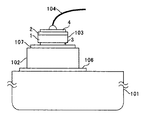
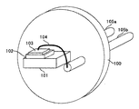
この図11のように構成される窒化物半導体レーザ素子がステムに設置されることによって、窒化物半導体レーザ装置が形成される。即ち、図3のように、ステム100に設けられたチップ搭載部101上の支持基体102上に窒化物半導体レーザ素子103が搭載される。この際、支持基体102とn電極510が接触するように設置され、窒化物半導体レーザ素子103を支持基体102上に固定するために、支持基体102の設置面上をAuでメタライズして、n電極510を熱圧着させる。又、p電極508はAu線であるワイヤ104を介してピン105bと電気的に接続される。尚、ピン105aは、チップ搭載部101及び支持基体102と電気的に接続される。ピン105a,105bは、ステム100と電気的に絶縁されている。
【0005】
このように窒化物半導体レーザ装置が構成されるとき、ピン105a,105bに異なる電位の電圧を印加して、窒化物半導体レーザ素子103のn電極510及びp電極508に電圧を印加することによって、窒化物半導体レーザ素子103がレーザー発振動作を行う。
【0006】
又、従来より使用されているGaAs系の半導体レーザ装置の場合、半導体レーザ素子が搭載される支持基体(図3の支持基体102に相当する)は、半導体レーザ素子の基板として用いられるGaAsと熱膨張係数が極力近く、熱伝導率が高い材質(例えば、SiC)が用いられていた。これは、GaAs系の半導体レーザ装置の場合、半導体レーザ素子を構成するGaAsと大きく異なる熱膨張係数の材質が支持基体に用いられると、半導体レーザ素子を支持基体にハンダ付けしたときに、半導体レーザ素子に大きな応力が発生し、半導体レーザー素子に欠陥が生じて、そのレーザ発振寿命が短くなるからである。
【0007】
【発明が解決しようとする課題】
しかしながら、従来の技術で示されるような窒化物半導体レーザ装置においては、レーザ発振寿命は短かった。又、GaAs系の半導体レーザ素子と同様にして、図3の支持基体の材料としてSiCを用いた場合も、そのレーザ発振寿命が短くなる。
【0008】
このような問題を鑑みて、本発明は、レーザ発振寿命の長い窒化物半導体レーザ装置を提供することを目的とする。
【0009】
【課題を解決するための手段】
上記目標を達成するために、本発明の窒化物半導体レーザ装置は、窒化物半導体基板と該窒化物半導体基板の表面上に積層される複数の窒化物半導体層から成る窒化物半導体積層部とを備えた窒化物半導体レーザ素子と、該窒化物半導体レーザ素子を固定する支持基体とを備えた窒化物半導体レーザ装置において、前記窒化物半導体基板がGaNから構成され、前記支持基体が、熱膨張係数が前記窒化物半導体基板の熱膨張係数よりも大きい材質で構成されるとともに、その厚さが前記窒化物半導体基板と前記窒化物半導体積層部とで成る窒化物半導体積層構造部の厚さの1.2倍以上であることを特徴とする。
【0010】
また、前記支持基体はCu,GaAs,CuW 10 ,Al 2 O 3 ,CuW 15 ,BeO,CuW 20 ,Al−SiC,Fe,Au,Ag,Alのうちのいずれかから構成してもよく、前記窒化物半導体積層部はAl x Ga y In z N(0≦x≦1,0≦y≦1,0≦z≦1,x+y+z=1)から構成してもよい。このとき、前記窒化物半導体積層構造部と前記支持基体との間の金属層の厚さを、前記窒化物半導体積層構造部の厚さの半分以下とすることによって、前記窒化物半導体レーザ素子の熱膨張係数と前記支持基体の熱膨張係数との違いによる前記窒化物半導体レーザ素子への効果を強くすることができる。
【0011】
又、前記窒化物半導体レーザ素子を前記支持基体に固定するためのハンダの材質に、AuSn、In、Sn、Pb、InAl、AgSn、AgCuSn、ZnSn、PbIn、PbSn、InSn、AuSi若しくはAuGe、又はこれらのいずれかを含む化合物を用いる。このようなハンダにおいて、融点の高い材質のものとしても良い。
【0012】
又、前記支持基体を備えたステムを有するとともに、前記支持基体がサブマウントであり、前記サブマウントを固定するチップ搭載部が前記ステムに設けられるようにしても構わない。即ち、前記チップ搭載部に、前記窒化物半導体レーザ素子がマウントされた前記支持基体となる前記サブマウントを設置することによって、窒化物半導体レーザ装置を構成する。このとき、前記サブマウントに前記窒化物半導体レーザ素子を固定するためのハンダの融点を、前記チップ搭載部に前記サブマウントを固定するためのハンダの融点より高くすることで、前記窒化物半導体レーザ素子を前記サブマウントに固定した後、該サブマウントを前記チップ搭載部に固定することができる。
【0013】
又、前記支持基体を備えたステムを有するとともに、前記支持基体が前記ステムに設けられたチップ搭載部とすることで、前記サブマウントを省き、窒化物半導体レーザ装置の製造工程を少なくすることができる。
【0014】
又、前記窒化物半導体レーザ素子の前記窒化物半導体基板側が前記支持基体に固定されるようにしても構わない。このとき、前記窒化物半導体基板と前記支持基体との間の金属層の厚さが、1μm以上50μm以下とする。
【0015】
又、前記窒化物半導体レーザ素子の前記窒化物半導体積層部側が前記支持基体に固定されるようにしても構わない。このとき、前記窒化物半導体レーザ素子の支持基体に固定される側が平坦に形成されており、前記窒化物半導体積層部と前記支持基体との間の金属層の厚さが、1μm以上10μm以下とする。
【0016】
【発明の実施の形態】
本発明の実施形態について、図面を参照して説明する。図1は、本発明の窒化物半導体レーザ装置に設けられる窒化物半導体レーザ素子の構成を示した断面図である。まず、この図1に示す窒化物半導体レーザ素子の構成について、以下に説明する。
【0017】
図1の窒化物半導体レーザ素子は、n型GaN基板1の表面上に、n型AlGaInNバッファ層201、n型AlGaInNコンタクト層202、n型AlGaInNクラッド層203、n型AlGaInNガイド層204、AlGaInN多重量子井戸活性層205、p型AlGaInNガイド層206、p型AlGaInNクラッド層207及びp型AlGaInNコンタクト層208が順に積層されるとともに、p型AlGaInNクラッド層207の表面上で且つp型AlGaInNクラッド層207及びp型AlGaInNコンタクト層208で構成されるリッジ部分210の両側に絶縁膜209が設けられる。
【0018】
又、この窒化物半導体レーザ素子は、n型GaN基板1の裏面側にn電極3が設けられるとともに、p型AlGaInNコンタクト層208及び絶縁膜209の表面上にp電極4が設けられる。尚、リッジ部分210は、共振器方向に延伸したストライプ状の構成である。よって、図1の窒化物半導体レーザ素子は、リッジストライプ型の構造となる。
【0019】
この窒化物半導体レーザ素子は、最初にn型GaN基板1を有機洗浄する。そして、n型GaN基板1をMOCVD(Metal Organic Chemical Vapor Deposition)装置内に搬入し、各層毎に、適切な基板温度にて、原料ガス及びキャリアガスを適量導入することによって、n型AlGaInNバッファ層201、n型AlGaInNコンタクト層202、n型AlGaInNクラッド層203、n型AlGaInNガイド層204、AlGaInN多重量子井戸活性層205、p型AlGaInNガイド層206、p型AlGaInNクラッド層207及びp型AlGaInNコンタクト層208が順に積層される。
【0020】
このとき、n型AlGaInNクラッド層203が、後述するn型AlGaInNガイド層204に比べて、屈折率が小さく且つバンドギャップが大きくなるように形成され、又、p型AlGaInNクラッド層207が、後述するp型AlGaInNガイド層206に比べて、屈折率が小さく且つバンドギャップが大きくなるように形成される。又、AlGaInN多重量子井戸活性層205は、障壁層及び井戸層が交互に複数層を設けられることによって形成される。
【0021】
そして、共振器方向に沿ってストライプ状にエッチングが行われて、リッジ部分210を形成すると、SiO2などの絶縁膜209を蒸着させて形成した後、p型AlGaInNコンタクト層208を露出させる。このようにして各層が形成されるとき、n型AlGaInNバッファ層201、n型AlGaInNコンタクト層202、n型AlGaInNクラッド層203、n型AlGaInNガイド層204、AlGaInN多重量子井戸活性層205、p型AlGaInNガイド層206、p型AlGaInNクラッド層207、p型AlGaInNコンタクト層208及び絶縁膜209で構成される部分を、窒化物半導体積層部2とする。
【0022】
この窒化物半導体積層部2が、n型GaN基板1の表面上に形成されるとき、n型GaN基板1の厚さが350μmであり、窒化物半導体積層部2の厚さが10μmである。その後、Pd/Mo/Auの順で蒸着して積層させて、p電極4を形成する。このとき、p電極4において、Pd/Mo/Auの層厚はそれぞれ、150Å/150Å/200Åとなる。
【0023】
次に、研削や研磨等の物理的手法や、ウェットエッチング又はドライエッチング等の化学的手法を用いることで、n型GaN基板1の裏面側を削って、n型GaN基板1と窒化物半導体積層部2とp電極4で構成されるウェハの厚さを40〜250μmに調整する。このようにすることで、ウェハを分割しやすい厚さに調整する。このとき、特に、端面ミラーも分割時に形成する場合には、40〜200μmと薄めに調整することが望ましい。尚、第1の実施形態で使用する場合、研削機を用いてウェハの厚みを180μmに調整した後、研磨機を用いてウェハの厚みを150μmに調整した。
【0024】
次に、n型GaN基板1の裏面側からTi/Al/Mo/Pt/Auの順序でn電極3を、真空蒸着法やイオンプレーティング法やスパッタ法などを用いて形成する。このとき、n電極3において、Ti/Al/Mo/Pt/Auの厚さはそれぞれ、300Å/1500Å/80Å/150Å/1500Åとなる。そして、Ti/Alはn型GaN基板1とのオーミック接触をとるための層であり、MoはAuとAlとが合金化することを防止するためのブロック層であり、Ptはハンダがn電極3のコンタクトをとる部分との反応が進みすぎないようにするための層であり、Auは支持部材上にマウントして設置する際にハンダと混合させて強固に設置するための層である。
【0025】
このように、n型GaN基板1に、窒化物半導体積層部2とn電極3とp電極4とを形成すると、共振器方向と垂直な方向に分割を行う。このとき、裏面側となるn電極3を上にして、n型GaN基板1と窒化物半導体積層部2とn電極3とp電極4とで構成されるウェハを、ダイヤモンド刃を備え溝を切るための装置であるダイサーなどに固定すると、ダイヤモンド針で罫書きするスクライブが施されることで、スクライブラインが設けられる。
【0026】
そして、ウェハにブレーキング刃などで力を加えることによって、スクライブラインに沿ってウェハを分割する。その後、同様に、共振器方向と平行な方向にブレーキング刃などで力を加えて更に分割することで、図1のような窒化物半導体レーザ素子を得ることができる。尚、上述のようにスクライビング法によるチップの分割を行うようにしたが、ワイヤソー又は薄板ブレードを用いて傷入れもしくは切断を行うダイシング法、エキシマレーザなどのレーザ光の照射加熱とその後の急冷により照射部にクラックを生じさせてスクライブラインを生成するレーザスクライビング法、高エネルギー密度のレーザ光を照射して照射部分を蒸発させて溝入れ加工を行うレーザアブレーション法などを用いても構わない。
【0027】
以下の第1及び第2の実施形態では、このように構成される窒化物半導体レーザ素子を備えた窒化物半導体装置について、図面を参照して説明する。
【0028】
<第1の実施形態>
本発明の第1の実施形態について、図面を参照して説明する。図2は、本実施形態の窒化物半導体レーザ装置において、窒化物半導体レーザ素子の設置状態を示す断面図である。このとき、図3のように、窒化物半導体レーザ素子が設けられることによって、窒化物半導体レーザ装置が構成される。尚、支持基体は、本実施形態において、「サブマウント」である。
【0029】
本実施形態の窒化物半導体レーザ装置は、図2のように、図3のステム100に突起するように形成されたチップ搭載部101の表面上にハンダ106で固定されたサブマウント102の表面上に、窒化物半導体レーザ素子103がハンダ107によって固定される。即ち、サブマウント102が、図3に示すようにピン105aと電気的に接続されたチップ搭載部101と、ハンダ106を介して電気的に接続されるとともに、チップ搭載部101の表面上に固定される。
【0030】
まず、サブマウント102の表面上に、ダイボンディング法を用いて、窒化物半導体レーザ素子103がマウントされる。即ち、サブマウント102の表面上にハンダ107を塗布して、ハンダ107の融点より若干高い温度まで加熱させてハンダ107を溶かした後、窒化物半導体レーザ素子103をn電極3がサブマント102側になるように載せる。そして、温度を1分程度保持しながら適当な荷重を加えることによって、n電極3とハンダ107とを良くなじませる。これにより、n電極3の最表面のAu層がハンダ107中に溶解して、ハンダ材料との合金が形成される。尚、逆に、ハンダ107を窒化物半導体レーザ素子103に塗布した後に、サブマウント102の表面上に設置するようにしても構わない。
【0031】
引き続き、窒化物半導体レーザ素子103が表面上にハンダ107によって接着固定されたサブマウント102が、チップ搭載部101の表面上に、ハンダ106を用いて接着固定される。そして、図3のようにピン105bと接続されたワイヤ104が、窒化物半導体レーザ素子103のp電極4に接続されることによって、ピン105bと窒化物半導体レーザ素子103のp電極4とが電気的に接続される。このようにして、窒化物半導体レーザ素子103がステム100に設置されると、窒素ガス封入のため、不図示のキャップがステム100に施される。
【0032】
このように窒化物半導体レーザ装置が構成されるとき、本実施形態では、ハンダ106の材料としてAgCuSnを用いるとともに、ハンダ107の材料としてAuSnを用いた。又、サブマウント102については、その材料を、n型GaN基板1の熱膨張率の高い材料であるCuとするとともに、その表面及び裏面上に、各層厚がそれぞれ0.4μm/0.1μmとなるNi/Auを順にメッキ形成した。又、サブマウント102に窒化物半導体レーザ素子103を設置する際、ハンダ107を融解するための温度を、350℃程度とした。
【0033】
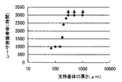
このように窒化物半導体レーザ装置を構成したとき、ハンダ107を含むn型GaN基板1とサブマウント102との間の金属層の層厚を10μmとし、サブマウント102の厚さを70μmから1mmまで変化させたときのレーザ発振寿命が、図4のようになる。又、このとき、上述したように、窒化物半導体レーザ素子103のn型GaN基板1と窒化物半導体積層部2とによる窒化物半導体積層構造の厚さを150μmとする。尚、図4は、横軸が対数軸となっている。又、レーザ発振寿命は、光出力を30mWとした状態で、APC(Auto Power Controll)駆動させたときの窒化物半導体レーザ素子が駆動可能な連続時間を表す。
【0034】
図4のグラフより明らかなように、支持基体であるサブマウント102の厚さが、窒化物半導体積層構造の厚さの1.2倍となる180μm以上となれば、レーザ発振寿命が1600時間以上となり、レーザ発振寿命が長くなることがわかる。更に、サブマウント102の厚さが厚くなるほどレーザ発振寿命が長くなり、窒化物半導体積層構造の厚さの2倍となる300μm以上となると、レーザ発振寿命が3000時間を超えることがわかる。
【0035】
この結果は、窒化物半導体積層構造の厚さを50〜350μmの間で変化させて同様の実験を行ったとき、同様の結果が得られた。即ち、サブマウント102の厚さを、窒化物半導体積層構造の厚さの1.2倍以上とすることでレーザ発振寿命が長くなり、更に、窒化物半導体積層構造の厚さの2倍以上とすることで更にレーザ発振寿命を長くすることができる。
【0036】
このように支持基体であるサブマウント102の厚さを厚くすることによってレーザ発振寿命が長くなる理由として、サブマウント102の材料に、その熱膨張係数が、窒化物半導体積層構造の主要構成要素である窒化物半導体基板(本実施形態においては、GaN基板1)として用いられるGaNの熱膨張係数より大きい材料となるCuが用いられていることが挙げられる。即ち、比較例として、GaNの熱膨張係数より小さい材料であるSiCを支持基体として用いた場合において、本実施形態と同様のレーザ寿命の実験を行った場合、図12に示すようになり、レーザ発振寿命が短くなる。尚、図6に、各材料の熱膨張係数を表示する。図6に示すように、Cuの熱膨張係数は17×10-6[1/K]であり、GaNの熱膨張係数5.6×10-6[1/K]に比べて大きい、一方、SiCの熱膨張係数は3.7×10-6[1/K]であり、GaNの熱膨張係数に比べて小さい。
【0037】
このように、GaNの熱膨張係数より大きい熱膨張係数の材料が用いられたとき、窒化物半導体レーザ素子103には、サブマウント102にマウントした後、圧縮性の応力がかかっていることとなる。このように窒化物半導体レーザ素子103に圧縮性の応力がかかる状態になる場合、マウント前に比べてマウント後の方が、窒化物半導体レーザ素子103の発振閾値電流値が低くなるという現象が生じる。これにより、レーザ発振寿命が長くなると考えられる。尚、支持基体であるサブマウント102の厚さが1.2倍以下となるときは、窒化物半導体レーザ素子103のマウント後、サブマウント102が歪むことによって応力が吸収されるため、レーザ発振寿命を長くするという効果が得られない。
【0038】
尚、本実施形態では、サブマウント102の材料としてCuを用いたが、その熱膨張係数がGaNの熱膨張係数よりも大きい材料、例えば、図6に示すGaAs、CuW10、Al2O3、CuW15、BeO、CuW20、Al−SiC、Fe、Au、Ag、Alなどでも構わない。又、これらの中で、熱伝導率が大きい材質は、放熱特性が良好であり好ましい。更に、このサブマウント102は、その表面にAuなどの薄膜が形成されていても構わない。尚、用いる材料の電気伝導性が低い場合は、サブマウント102の窒化物半導体レーザ素子103をマウントしている面とチップ搭載部101の間をワイヤーで配線し、電気的接続を取るようにすると良い。
【0039】
又、このようにサブマウント102にGaNの熱膨張係数より高いCuが材料として用いられたとき、窒化物半導体レーザ素子103のn型GaN基板1と窒化物半導体積層部2とによる窒化物半導体積層構造及びサブマウント102の厚さをそれぞれ150μm及び300μmとし、ハンダ107を含むn型GaN基板1とサブマウント102との間の金属層の層厚を0.7μmから150μmまで変化させたときのレーザ発振寿命が、図5のようになる。
【0040】
尚、このとき、金属層の層厚が数十μm以下の薄い場合には、サブマウント102又は窒化物半導体レーザ素子103の接着面に、AuSnハンダを蒸着又はスパッタにより形成する。又、金属層の層厚が数十μm以上と厚い場合は、箔状になっているAuSn箔をサブマウント102と窒化物半導体レーザ素子103との間に設置してマウントを行う。又、図5は、横軸が対数軸となっている。
【0041】
図5のグラフより明らかなように、ハンダ107を含むn型GaN基板1とサブマウント102との間の金属層の層厚が1〜50μmであれば、レーザ発振寿命が1600時間以上となり、レーザ発振寿命が長くなることがわかる。特に、金属層の層厚が3〜10μmであるとき、レーザ発振寿命が3000時間を超えることがわかる。尚、サブマント102の厚さを、窒化物半導体積層構造の厚さの1.2倍以上としたとき、この結果と同様の結果が得られた。
【0042】
このような結果が得られるのは、金属層の層厚が50μmを超えると、サブマウント102上に窒化物半導体レーザー素子103をマウントしたときに、窒化物半導体レーザ素子103にかかる圧縮性の応力がハンダ107によって吸収されてしまうことと、金属層の層厚が1μmよりも薄いときには、サブマウント102と窒化物半導体レーザ素子103との密着性が悪く、放熱性が悪くなってしまうこととが原因と考えられる。よって、ハンダ107を含むn型GaN基板1とサブマウント102との間の金属層の層厚が1μmより薄いとき、又は、50μmを超えるときは、それぞれ、レーザ発振寿命が短くなってしまう。
【0043】
尚、本実施形態では窒化物半導体レーザ素子103をサブマウント102に接着するためのハンダ107として、AuSnを用いたが、例えば、In、Sn、Pb、InAl、AgSn、AgCuSn、ZnSn、PbIn、PbSn、InSn、AuSi、AuGe等のハンダ、又は、これらの化合物よりなるハンダを用いても構わない。又、融点が高いハンダ材料や接着強度が強いハンダ材料であることが好ましいことから、例えば、ハンダ107として、AgSn、AgCuSn、AuSi、AuGe、PbSn、InSnなどが挙げられる。
【0044】
又、本実施形態では、サブマウント102の表面にNi/Auが順にそれぞれ層厚が0.4μm/0.1μmでメッキ形成されるようにしているが、ハンダ107によるサブマウント102と窒化物半導体レーザ素子103との接着性に対して必要な特性が保たれるのであれば、サブマウント102の表面上において、他の材料及び構造としても構わない。
【0045】
又、サブマウント102をチップ搭載部101上に固定するために使用されるハンダ106として、AgCuSnを用いたが、例えば、PbSn、AgSn、ZnSn、In、Pbなどの他の材料系のハンダを使用しても構わない。但し、本実施形態では、窒化物半導体レーザ素子103をサブマウント102にマウントした後に、このサブマウント102をチップ搭載部101に固定するため、窒化物半導体レーザ素子103をサブマウント102に固定するために用いるハンダ107の融点よりも低い融点の材料をハンダ106に用いることが好ましい。
【0046】
本実施形態では、支持基体としてサブマウントを用いるため、チップ搭載部に比べてサブマウントの表面の加工精度が高いので、窒化物半導体レーザ素子と支持基体とをより強固に確実に密着することができる。よって、特性の良好な窒化物半導体レーザ装置とすることができる。
【0047】
<第2の実施形態>
本発明の第2の実施形態について、図面を参照して説明する。図7は、本実施形態の窒化物半導体レーザ装置において、窒化物半導体レーザ素子の設置状態を示す断面図である。このとき、図8のように、窒化物半導体レーザ素子が設けられることによって、窒化物半導体レーザ装置が構成される。尚、支持基体は、本実施形態において、「チップ搭載部」である。又、図7及び図8のそれぞれにおいて、図2及び図3のそれぞれにおける部分と同一の部分については、同一の符号を付してその詳細な説明は省略する。
【0048】
本実施形態の窒化物半導体レーザ装置は、図7及び図8のように、ステム100に突起するように形成されたチップ搭載部101の表面上に、窒化物半導体レーザ素子103がハンダ106によって固定される。その他の構成については、第1の実施形態と同様となるので、説明を省略する。
【0049】
このように窒化物半導体レーザ装置を構成したとき、チップ搭載部101の厚さを、窒化物半導体レーザ素子103のn型GaN基板1と窒化物半導体積層部2とによる窒化物半導体積層構造の厚さの1.2倍以上(特には、2倍以上)とするとともに、チップ搭載部101として、その熱膨張係数がGaNの熱膨張係数よりも大きい材料を用いる。又、ハンダ106を含むn型GaN基板1とチップ搭載部101との間の金属層の層厚を、1〜50μmとする。このようにすることで、窒化物半導体レーザ素子103をチップ搭載部101にマウントしたとき、窒化物半導体レーザ素子103に圧縮性の応力がかかり、レーザ発振寿命が長くなる。
【0050】
尚、本実施形態では、窒化物半導体レーザ素子103の窒化物半導体積層構造の厚さを200μmとし、ハンダ106の材料にAgCuSnを用いるとともにハンダ106を含むn型GaN基板1とチップ搭載部101との間の金属層の層厚を20μmとした。又、チップ搭載部101については、その材料をCuとし、その表面には、蒸着により、Mo/Auの順に、それぞれの層厚が0.4μm/0.03μmとなるように形成する。又、チップ搭載部101の厚さは1000μmとした。更に、このチップ搭載部101はステム100に溶接されることで固定されている。このように構成した窒化物半導体レーザ装置のレーザ発振寿命は3000時間以上となった。
【0051】
尚、本実施形態において、窒化物半導体レーザ素子103をチップ搭載部101に接着するためのハンダ106として、AgCuSnを用いたが、例えば、In、Sn、Pb、InAl、AgSn、AuSn、ZnSn、PbIn、PbSn、InSn、AuSi、AuGe等のハンダ、又は、これらの化合物よりなるハンダを用いても構わない。又、融点が高いハンダ材料や接着強度が強いハンダ材料であることが好ましいことから、例えば、ハンダ106として、AuSn、AgSn、AuSi、AuGe、PbSn、InSnなどが挙げられる。
【0052】
又、本実施形態では、チップ搭載部101の表面にMo/Auが順にそれぞれ層厚が0.4μm/0.03μmでメッキ形成されるようにしているが、ハンダ106によるチップ搭載部101と窒化物半導体レーザ素子103との接着性に対して必要な特性が保たれるのであれば、チップ搭載部101の表面上において、他の材料及び構造としても構わない。
【0053】
更に、第1の実施形態と同様、チップ搭載部101の材料として、Cu以外に、熱膨張係数がGaNの熱膨張係数よりも大きい材料、例えば、図6に示すGaAs、CuW10、Al2O3、CuW15、BeO、CuW20、Al−SiC、Fe、Au、Ag、Alなどでも構わない。又、これらの中で、熱伝導率が大きい材質は、放熱特性が良好であり好ましい。更に、このチップ搭載部101は、その表面にAuなどの薄膜が形成されていても構わない。尚、用いる材料の電気伝導性が低い場合は、表面に金属層を形成し、或いは、更に配線を施すことにより電気的接続を取るようにすると良い。
【0054】
本実施形態では、支持基体としてチップ搭載部を用いるため、サブマウントを用いたときに比べて、窒化物半導体レーザ装置を製造するための工程が少なくなる。
【0055】
尚、第1及び第2の実施形態において、窒化物半導体レーザ素子103のn電極3として、それぞれの厚さが300Å/1500Å/80Å/150Å/1500ÅとなるTi/Al/Mo/Pt/Auを、n型GaN基板1側から順に積層したが、それぞれに必要な特性さえ保たれていれば、他の材料及び構造としても構わない。例えば、n型GaN基板1とのオーミック接触をとるための層であるTi/Alの部分を、例えば、Hf/Au等の層を用いても構わない。
【0056】
又、上述の第1及び第2の実施形態では、窒化物半導体レーザ素子を支持基体にマウントする際、n型GaN基板の裏面に設けられたn電極側が支持基体に接するようなジャンクションアップの形でマウントした場合について述べた。以下の第3の実施形態では、窒化物半導体レーザ素子を支持基体にマウントする際、窒化物半導体積層部の表面に設けられたp電極側が支持基体に接するようなジャンクションダウンの形でマウントした場合について述べる。
【0057】
<第3の実施形態>
本発明の第3の実施形態について、図面を参照して説明する。図9は、本実施形態の窒化物半導体レーザ装置に備えられる窒化物半導体レーザ素子の構成を示す断面図である。又、図10は、本実施形態の窒化物半導体レーザ装置において、窒化物半導体レーザ素子の設置状態を示す断面図である。このとき、第1の実施形態と同様、図3のように、窒化物半導体レーザ素子が設けられることによって、窒化物半導体レーザ装置が構成される。尚、支持基体は、本実施形態において、「サブマウント」である。又、図9及び図10において、図1及び図2における部分と同一の部分については、同一の符号を付してその詳細な説明は省略する。
【0058】
図9の窒化物半導体レーザ素子は、図1の窒化物半導体レーザ素子と同様、n型GaN基板1の表面に、n型AlGaInNバッファ層201、n型AlGaInNコンタクト層202、n型AlGaInNクラッド層203、n型AlGaInNガイド層204、AlGaInN多重量子井戸活性層205、p型AlGaInNガイド層206、p型AlGaInNクラッド層207及びp型AlGaInNコンタクト層208が順に積層される。又、p型AlGaInNクラッド層207の表面上で且つp型AlGaInNクラッド層207及びp型AlGaInNコンタクト層208で構成されるリッジ部分210の両側に絶縁膜209が設けられる。
【0059】
そして、この窒化物半導体レーザ素子は、n型GaN基板1の裏面側にn電極3が設けられるとともに、p型AlGaInNコンタクト層208及び絶縁膜209の表面上にp電極4aが設けられる。このとき、p電極4aは、図1のp電極4のようにリッジ部分210に対応する部分が凸状とされるのではなく、支持基体に接するように全体が平坦となるように形成される。このように構成される窒化物半導体レーザ素子において、窒化物半導体積層部2の厚さを10μmとする。
【0060】
図9のように構成される窒化物半導体レーザ素子103aを、図10のように、ジャンクションダウンの方式で、第1の実施形態(図2)と同様、ハンダ107によって、サブマウント102に固定する。よって、本実施形態では、第1の実施形態と異なり、p電極4a側がサブマウント102にマウントされた面となる。又、図3のようにピン105bと接続されたワイヤ104が、窒化物半導体レーザ素子103aのn電極3に接続されることによって、ピン105bと窒化物半導体レーザ素子103aのn電極3とが電気的に接続される。
【0061】
このように窒化物半導体レーザ装置を構成する際、本実施形態では、窒化物半導体レーザ素子103aのn型GaN基板1と窒化物半導体積層部2とによる窒化物半導体積層構造の厚さを200μmとする。このとき、窒化物半導体レーザ素子103aのp電極4aを、Pd/Mo/Au/Pt/Auの順で蒸着して積層することで構成し、Pd/Mo/Au/Pt/Auの層厚をそれぞれ、150Å/150Å/2000Å/150Å/1500Åとする。
【0062】
又、サブマウント102については、その材料を、n型GaN基板1の熱膨張率の高い材料であるCuとするとともに、その表面及び裏面上に、各層厚がそれぞれ0.4μm/0.03μmとなるMo/Auを順に蒸着し、サブマウント102の厚さを400μmとした。又、サブマウント102の表面上には、窒化物半導体積層部2とサブマウント102との間の金属層が、AuSnのハンダ107を含を含んで1.5μm形成され、このハンダ107によって、窒化物半導体レーザ素子103aがサブマウント102の表面上に接着される。更に、この窒化物半導体レーザ素子103aがマウントされたサブマウント102は、ZnSnのハンダ106によって、チップ搭載部101の表面上に固定される。
【0063】
このように構成した窒化物半導体レーザ装置のレーザ発振寿命は3000時間以上となった。よって、このことより、ジャンクションアップの状態で窒化物半導体レーザ素子を設置した場合だけでなく、ジャンクションダウンの状態で窒化物半導体レーザ素子を設置した場合においても、レーザ発振寿命を長寿命化することができる。特に、本実施形態のようにジャンクションダウンの状態で設置した場合、ジャンクションアップの状態で設置した場合に比べて、発光する領域により効率よく応力を伝えることができるとともに、発光する領域にて発生する熱を支持基体に効率的に放熱できるので、より長寿命の効果を得ることができる。
【0064】
尚、本実施形態では、サブマウント102を上述のような構成としたが、第1の実施形態と同様、その熱膨張係数が、窒化物半導体積層構造の主要構成要素である窒化物半導体基板(本実施形態においては、GaN基板1)としてのGaNの熱膨張係数より大きく、又、その厚さが窒化物半導体レーザ素子の窒化物半導体積層構造の厚さの1.2倍以上となればよい。又、ハンダ106,107についても、第1の実施形態と同様の条件を満たすものであれば良く、上述の材料に限定されるものではない。
【0065】
又、本実施形態では、ジャンクションダウンの形で窒化物半導体レーザ素子103aを支持基体に接着させるため、ハンダ107の層厚が厚いと、窒化物半導体レーザ素子103aのpn接合面にハンダ107が接触してしまい、半導体装置として動作できなくなることがあるので、第1の実施形態と異なり、ハンダ107を含むn型GaN基板1とサブマウント102との間の金属層は、pn接合面にハンダが接触しないように、1〜10μmとすることが必要である。
【0066】
更に、本実施形態では、支持基体としてサブマウントを利用したものとしたが、第2の実施形態と同様、支持基体をチップ搭載部として、直接、窒化物半導体レーザ素子をチップ搭載部にマウントするようにしても構わない。このとき、チップ搭載部及びチップ搭載部に窒化物半導体レーザ素子をマウントさせるためのハンダの条件は、サブマウント及びチップ搭載部に窒化物半導体レーザ素子をマウントさせるためのハンダの条件と同様となる。
【0067】
【発明の効果】
本発明によると、支持基体の厚さを窒化物半導体積層構造部の厚さの1.2倍以上とするとするとともに、支持基体の熱膨張係数を窒化物半導体積層構造部の主要構成要素である窒化物半導体基板の熱膨張係数より大きくすることによって、窒化物半導体レーザ素子に圧縮性の応力をかけられると考えられ、窒化物半導体レーザ素子のレーザ発振寿命を長くすることができる。又、支持基体と窒化物半導体積層構造部との間の金属層の厚さを窒化物半導体積層構造部の厚さの半分以下とすることで、窒化物半導体レーザ素子に圧縮性の応力を伝えやすくすることができる。
【図面の簡単な説明】
【図1】窒化物半導体レーザ素子の構成を示すための断面図。
【図2】第1の実施形態の窒化物半導体レーザ装置の構成を示す断面図。
【図3】窒化物半導体レーザ装置の構成の一例を示す斜視図。
【図4】本発明の窒化物半導体レーザ装置における支持基体の厚さに対するレーザ発振寿命の変化を示すグラフ。
【図5】窒化物半導体レーザ素子と支持基体との間の金属層厚に対するレーザ発振寿命の変化を示すグラフ。
【図6】各材質の熱膨張係数を表す図。
【図7】第2の実施形態の窒化物半導体レーザ装置の構成を示す断面図。
【図8】窒化物半導体レーザ装置の構成の一例を示す斜視図。
【図9】窒化物半導体レーザ素子の構成を示すための断面図。
【図10】第3の実施形態の窒化物半導体レーザ装置の構成を示す断面図。
【図11】窒化物半導体レーザ素子の構成を示すための断面図。
【図12】従来の窒化物半導体レーザ装置における支持基体の厚さに対するレーザ発振寿命の変化を示すグラフ。
【符号の説明】
1 n型GaN基板
2 窒化物半導体積層部
3 n電極
4,4a p電極[0001]
BACKGROUND OF THE INVENTION
The present invention relates to a nitride semiconductor laser device in which a nitride semiconductor laser element is provided on a support base. In this specification, a nitride semiconductor means Al.xGayInzN (0 ≦ x ≦ 1, 0 ≦ y ≦ 1, 0 ≦ z ≦ 1, x + y + z = 1). At this time, about 10% or less (however, being hexagonal) of the nitrogen element of the nitride semiconductor may be substituted with any element of As, P, and Sb. A nitride semiconductor may be doped with Si, O, Cl, S, C, Ge, Zn, Cd, Mg, and Be.
[0002]
[Prior art]
The semiconductor laser device emits strong light with good monochromaticity, so the spot size when the laser output light is condensed can be reduced, and recording and reproduction are performed by irradiating light from an optical disc or magneto-optical disc. Is used as a light source or the like provided in an optical pickup in a recording medium driving apparatus. In particular, a nitride semiconductor laser element having a short wavelength and capable of obtaining an optical output is being developed as an optical pickup element that replaces a red semiconductor laser element so as to be used for a drive device of a high-density recording medium such as a DVD. .
[0003]
Such a nitride semiconductor laser device is presented in Japanese Patent Laid-Open No. 11-340571. FIG. 11 shows the structure of the nitride semiconductor laser device disclosed in Japanese Patent Laid-Open No. 11-340571. The nitride semiconductor laser device shown in FIG. 11 has an n-
[0004]
A nitride semiconductor laser device is formed by installing the nitride semiconductor laser element configured as shown in FIG. 11 on the stem. That is, as shown in FIG. 3, the nitride
[0005]
When the nitride semiconductor laser device is configured in this way, by applying voltages of different potentials to the
[0006]
In the case of a GaAs semiconductor laser device conventionally used, the support base (corresponding to the
[0007]
[Problems to be solved by the invention]
However, the nitride semiconductor laser device as shown in the prior art has a short laser oscillation lifetime. Similarly to the GaAs-based semiconductor laser element, when SiC is used as the material of the supporting base shown in FIG. 3, the laser oscillation life is shortened.
[0008]
In view of such a problem, an object of the present invention is to provide a nitride semiconductor laser device having a long laser oscillation lifetime.
[0009]
[Means for Solving the Problems]
In order to achieve the above object, a nitride semiconductor laser device according to the present invention includes a nitride semiconductor substrate and a nitride semiconductor stacked portion including a plurality of nitride semiconductor layers stacked on the surface of the nitride semiconductor substrate. In a nitride semiconductor laser device comprising a nitride semiconductor laser element provided and a support base for fixing the nitride semiconductor laser element,The nitride semiconductor substrate is made of GaN;The support base has a thermal expansion coefficient.SaidThe nitride semiconductor substrate is made of a material having a thermal expansion coefficient larger than that of the nitride semiconductor substrate, and the thickness thereof is 1.2 of the thickness of the nitride semiconductor multilayer structure portion including the nitride semiconductor substrate and the nitride semiconductor multilayer portion. It is characterized by being more than double.
[0010]
The supporting base is Cu, GaAs, CuW. 10 , Al 2 O 3 , CuW 15 , BeO, CuW 20 , Al—SiC, Fe, Au, Ag, or Al, and the nitride semiconductor stacked portion is made of Al. x Ga y In z N (0 ≦ x ≦ 1, 0 ≦ y ≦ 1, 0 ≦ z ≦ 1, x + y + z = 1) may be used.At this time, the thickness of the metal layer between the nitride semiconductor multilayer structure portion and the support base is set to be equal to or less than half the thickness of the nitride semiconductor multilayer structure portion. The effect on the nitride semiconductor laser element due to the difference between the thermal expansion coefficient and the thermal expansion coefficient of the support base can be enhanced.
[0011]
In addition, a solder material for fixing the nitride semiconductor laser element to the support base,AuSn, In, Sn, Pb, InAl, AgSn, AgCuSn, ZnSn, PbIn, PbSn, InSn, AuSi or AuGe, or theseCompounds containing either are used. Such solder may be made of a material having a high melting point.
[0012]
Further, it may have a stem provided with the support base, the support base may be a submount, and a chip mounting portion for fixing the submount may be provided on the stem. That is, the nitride semiconductor laser device is configured by installing the submount serving as the support base on which the nitride semiconductor laser element is mounted on the chip mounting portion. At this time, by making the melting point of the solder for fixing the nitride semiconductor laser element to the submount higher than the melting point of the solder for fixing the submount to the chip mounting portion, the nitride semiconductor laser After fixing the element to the submount, the submount can be fixed to the chip mounting portion.
[0013]
Further, by having a stem provided with the support base, and the support base being a chip mounting portion provided on the stem, the submount can be omitted, and the number of manufacturing steps of the nitride semiconductor laser device can be reduced. it can.
[0014]
The nitride semiconductor laserelementThe nitride semiconductor substrate side may be fixed to the support base. At this time, the thickness of the metal layer between the nitride semiconductor substrate and the support base is 1 μm or more and 50 μm or less.
[0015]
The nitride semiconductor laserelementThe nitride semiconductor laminated portion side of the substrate may be fixed to the support base. At this time,The side fixed to the support base of the nitride semiconductor laser element is formed flat,The thickness of the metal layer between the nitride semiconductor laminated portion and the support base is 1 μm or more and 10 μm or less.
[0016]
DETAILED DESCRIPTION OF THE INVENTION
Embodiments of the present invention will be described with reference to the drawings. FIG. 1 is a cross-sectional view showing the configuration of a nitride semiconductor laser element provided in the nitride semiconductor laser device of the present invention. First, the structure of the nitride semiconductor laser element shown in FIG. 1 will be described below.
[0017]
1 includes an n-type
[0018]
In this nitride semiconductor laser element, the n-electrode 3 is provided on the back side of the n-
[0019]
In this nitride semiconductor laser device, the n-
[0020]
At this time, the n-type
[0021]
Then, etching is performed in a stripe shape along the resonator direction to form the ridge portion 210.2The p-type
[0022]
When the nitride semiconductor multilayer portion 2 is formed on the surface of the n-
[0023]
Next, the back side of the n-
[0024]
Next, the n electrode 3 is formed in the order of Ti / Al / Mo / Pt / Au from the back side of the n-
[0025]
As described above, when the nitride semiconductor multilayer portion 2, the n electrode 3, and the p electrode 4 are formed on the n-
[0026]
Then, the wafer is divided along the scribe line by applying a force to the wafer with a braking blade or the like. Thereafter, similarly, by applying a force with a braking blade or the like in a direction parallel to the resonator direction and further dividing, a nitride semiconductor laser device as shown in FIG. 1 can be obtained. In addition, as described above, the chip is divided by the scribing method, but irradiation is performed by a dicing method in which a wire saw or a thin blade is used to cut or cut, irradiation by laser light such as an excimer laser, and subsequent rapid cooling. A laser scribing method for generating a scribe line by generating a crack in the portion, a laser ablation method for performing irradiation by evaporating the irradiated portion by irradiating a laser beam with a high energy density, or the like may be used.
[0027]
In the following first and second embodiments, a nitride semiconductor device including the nitride semiconductor laser element configured as described above will be described with reference to the drawings.
[0028]
<First Embodiment>
A first embodiment of the present invention will be described with reference to the drawings. FIG. 2 is a cross-sectional view showing an installation state of the nitride semiconductor laser element in the nitride semiconductor laser device of this embodiment. At this time, as shown in FIG. 3, the nitride semiconductor laser device is configured by providing the nitride semiconductor laser element. The support base is a “submount” in the present embodiment.
[0029]
As shown in FIG. 2, the nitride semiconductor laser device of the present embodiment is on the surface of the
[0030]
First, the nitride
[0031]
Subsequently, the
[0032]
When the nitride semiconductor laser device is configured as described above, in this embodiment, AgCuSn is used as the material of the
[0033]
When the nitride semiconductor laser device is configured in this way, the thickness of the metal layer between the n-
[0034]
As is apparent from the graph of FIG. 4, when the thickness of the
[0035]
This result was obtained when the same experiment was performed by changing the thickness of the nitride semiconductor multilayer structure between 50 and 350 μm. That is, by making the thickness of the
[0036]
The reason why the laser oscillation lifetime is increased by increasing the thickness of the
[0037]
As described above, when a material having a thermal expansion coefficient larger than that of GaN is used, the nitride
[0038]
In this embodiment, Cu is used as the material of the
[0039]
In addition, when Cu having a thermal expansion coefficient higher than that of GaN is used as the material for the
[0040]
At this time, when the thickness of the metal layer is as small as several tens of μm or less, AuSn solder is formed on the adhesion surface of the
[0041]
As apparent from the graph of FIG. 5, when the thickness of the metal layer between the n-
[0042]
Such a result is obtained when the thickness of the metal layer exceeds 50 μm and compressive stress applied to the nitride
[0043]
In this embodiment, AuSn is used as the
[0044]
In the present embodiment, Ni / Au is plated on the surface of the
[0045]
In addition, AgCuSn is used as the
[0046]
In this embodiment, since the submount is used as the support base, the processing accuracy of the surface of the submount is higher than that of the chip mounting portion. Therefore, the nitride semiconductor laser element and the support base can be more firmly and securely adhered to each other. it can. Therefore, a nitride semiconductor laser device with good characteristics can be obtained.
[0047]
<Second Embodiment>
A second embodiment of the present invention will be described with reference to the drawings. FIG. 7 is a cross-sectional view showing an installation state of the nitride semiconductor laser element in the nitride semiconductor laser device of this embodiment. At this time, as shown in FIG. 8, the nitride semiconductor laser device is configured by providing the nitride semiconductor laser element. The support base is a “chip mounting portion” in the present embodiment. Further, in each of FIGS. 7 and 8, the same parts as those in FIGS. 2 and 3 are denoted by the same reference numerals, and detailed description thereof is omitted.
[0048]
In the nitride semiconductor laser device of this embodiment, the nitride
[0049]
When the nitride semiconductor laser device is configured as described above, the thickness of the
[0050]
In this embodiment, the thickness of the nitride semiconductor multilayer structure of the nitride
[0051]
In this embodiment, AgCuSn is used as the
[0052]
In the present embodiment, Mo / Au is plated on the surface of the
[0053]
Furthermore, as in the first embodiment, as a material for the
[0054]
In this embodiment, since the chip mounting portion is used as the support base, the number of steps for manufacturing the nitride semiconductor laser device is reduced as compared with the case where the submount is used.
[0055]
In the first and second embodiments, Ti / Al / Mo / Pt / Au each having a thickness of 300 mm / 1500 mm / 80 mm / 150 mm / 1500 mm is used as the n-electrode 3 of the nitride
[0056]
In the first and second embodiments described above, when the nitride semiconductor laser device is mounted on the support base, the n-electrode side provided on the back surface of the n-type GaN substrate is in contact with the support base. I described the case of mounting with. In the third embodiment below, when mounting a nitride semiconductor laser element on a support base, the p-electrode side provided on the surface of the nitride semiconductor multilayer portion is mounted in a junction-down manner so as to be in contact with the support base Is described.
[0057]
<Third Embodiment>
A third embodiment of the present invention will be described with reference to the drawings. FIG. 9 is a cross-sectional view showing the configuration of the nitride semiconductor laser element provided in the nitride semiconductor laser device of this embodiment. FIG. 10 is a cross-sectional view showing an installation state of the nitride semiconductor laser element in the nitride semiconductor laser device of this embodiment. At this time, as in the first embodiment, the nitride semiconductor laser device is configured by providing the nitride semiconductor laser element as shown in FIG. The support base is a “submount” in the present embodiment. 9 and 10, the same parts as those in FIGS. 1 and 2 are denoted by the same reference numerals, and detailed description thereof is omitted.
[0058]
The nitride semiconductor laser device of FIG. 9 is similar to the nitride semiconductor laser device of FIG. 1 in that an n-type
[0059]
In this nitride semiconductor laser device, the n-electrode 3 is provided on the back side of the n-
[0060]
The nitride
[0061]
When the nitride semiconductor laser device is configured as described above, in this embodiment, the thickness of the nitride semiconductor multilayer structure formed by the n-
[0062]
For the
[0063]
The nitride semiconductor laser device thus configured has a laser oscillation lifetime of 3000 hours or longer. Therefore, it is possible to extend the laser oscillation lifetime not only when the nitride semiconductor laser element is installed in the junction-up state but also when the nitride semiconductor laser element is installed in the junction-down state. Can do. In particular, when installed in a junction-down state as in this embodiment, stress can be transmitted more efficiently to the light-emitting region than in the case of installing in a junction-up state, and it occurs in the light-emitting region. Since heat can be efficiently radiated to the support base, a longer life effect can be obtained.
[0064]
In the present embodiment, the
[0065]
In this embodiment, since the nitride
[0066]
Further, in the present embodiment, the submount is used as the support base. However, as in the second embodiment, the nitride semiconductor laser device is directly mounted on the chip mount using the support base as the chip mount. It doesn't matter if you do. At this time, the solder conditions for mounting the nitride semiconductor laser device on the chip mounting portion and the chip mounting portion are the same as the solder conditions for mounting the nitride semiconductor laser device on the submount and the chip mounting portion. .
[0067]
【The invention's effect】
According to the present invention, the thickness of the support base is 1.2 times or more the thickness of the nitride semiconductor multilayer structure, and the thermal expansion coefficient of the support base is a main component of the nitride semiconductor multilayer structure. By making it larger than the thermal expansion coefficient of the nitride semiconductor substrate, it is considered that compressive stress can be applied to the nitride semiconductor laser element, and the laser oscillation lifetime of the nitride semiconductor laser element can be extended. In addition, compressive stress is transmitted to the nitride semiconductor laser device by making the thickness of the metal layer between the support base and the nitride semiconductor multilayer structure portion less than half the thickness of the nitride semiconductor multilayer structure portion. It can be made easier.
[Brief description of the drawings]
FIG. 1 is a cross-sectional view illustrating a configuration of a nitride semiconductor laser element.
FIG. 2 is a cross-sectional view showing the configuration of the nitride semiconductor laser device of the first embodiment.
FIG. 3 is a perspective view showing an example of the configuration of a nitride semiconductor laser device.
FIG. 4 is a graph showing a change in laser oscillation lifetime with respect to the thickness of a support base in the nitride semiconductor laser device of the present invention.
FIG. 5 is a graph showing a change in laser oscillation lifetime with respect to a metal layer thickness between a nitride semiconductor laser element and a support base.
FIG. 6 is a diagram showing a thermal expansion coefficient of each material.
FIG. 7 is a cross-sectional view showing a configuration of a nitride semiconductor laser device according to a second embodiment.
FIG. 8 is a perspective view showing an example of the configuration of a nitride semiconductor laser device.
FIG. 9 is a cross-sectional view showing a configuration of a nitride semiconductor laser element.
FIG. 10 is a cross-sectional view showing a configuration of a nitride semiconductor laser device according to a third embodiment.
FIG. 11 is a cross-sectional view showing the configuration of a nitride semiconductor laser element.
FIG. 12 is a graph showing a change in laser oscillation lifetime with respect to the thickness of a support base in a conventional nitride semiconductor laser device.
[Explanation of symbols]
1 n-type GaN substrate
2 Nitride semiconductor stack
3 n electrode
4,4ap electrode
Claims (6)
当該窒化物半導体レーザ素子の前記窒化物半導体基板側が前記支持基体に固定され、
前記窒化物半導体基板がGaNから構成され、
前記支持基体が、サブマウントであって、Cuで構成されるとともに、その厚さが前記窒化物半導体基板と前記窒化物半導体積層部とで成る窒化物半導体積層構造部の厚さの2倍以上であり、
前記サブマウントを固定するチップ搭載部が前記ステムに設けられ、
前記窒化物半導体レーザ素子に圧縮性応力がかかっていることを特徴とする窒化物半導体レーザ装置。A nitride semiconductor laser device comprising a nitride semiconductor substrate and a nitride semiconductor laminated portion composed of a plurality of nitride semiconductor layers laminated on the surface of the nitride semiconductor substrate, and fixing the nitride semiconductor laser device In a nitride semiconductor laser device including a support base and a stem including the support base ,
The nitride semiconductor substrate side of the nitride semiconductor laser element is fixed to the support base,
The nitride semiconductor substrate is made of GaN;
The support base is a sub-mount, while being composed of Cu, 2 times or more the thickness of the thickness of the nitride semiconductor laminated structure formed of said nitride semiconductor substrate and the nitride semiconductor lamination portion der is,
A chip mounting portion for fixing the submount is provided on the stem,
A nitride semiconductor laser device, wherein compressive stress is applied to the nitride semiconductor laser element .
Priority Applications (2)
| Application Number | Priority Date | Filing Date | Title |
|---|---|---|---|
| JP2001295939A JP4514376B2 (en) | 2001-09-27 | 2001-09-27 | Nitride semiconductor laser device |
| US10/255,062 US6895029B2 (en) | 2001-09-27 | 2002-09-26 | Nitride semiconductor laser device |
Applications Claiming Priority (1)
| Application Number | Priority Date | Filing Date | Title |
|---|---|---|---|
| JP2001295939A JP4514376B2 (en) | 2001-09-27 | 2001-09-27 | Nitride semiconductor laser device |
Publications (3)
| Publication Number | Publication Date |
|---|---|
| JP2003101113A JP2003101113A (en) | 2003-04-04 |
| JP2003101113A5 JP2003101113A5 (en) | 2005-10-13 |
| JP4514376B2 true JP4514376B2 (en) | 2010-07-28 |
Family
ID=19117286
Family Applications (1)
| Application Number | Title | Priority Date | Filing Date |
|---|---|---|---|
| JP2001295939A Expired - Fee Related JP4514376B2 (en) | 2001-09-27 | 2001-09-27 | Nitride semiconductor laser device |
Country Status (2)
| Country | Link |
|---|---|
| US (1) | US6895029B2 (en) |
| JP (1) | JP4514376B2 (en) |
Families Citing this family (20)
| Publication number | Priority date | Publication date | Assignee | Title |
|---|---|---|---|---|
| JP2006179508A (en) * | 2003-03-06 | 2006-07-06 | Matsushita Electric Ind Co Ltd | Method for preventing degrading of nitride-based group iii-v compound semiconductor light-emitting device |
| US7247514B2 (en) * | 2003-04-11 | 2007-07-24 | Matsushita Electric Industrial Co., Ltd. | Semiconductor device and method for producing the same |
| JP4072093B2 (en) * | 2003-05-20 | 2008-04-02 | 株式会社日立製作所 | Semiconductor laser module |
| KR100542720B1 (en) * | 2003-06-03 | 2006-01-11 | 삼성전기주식회사 | GaN-based Semiconductor junction structure |
| JP2005026291A (en) * | 2003-06-30 | 2005-01-27 | Sharp Corp | Nitride-based semiconductor light emitting device and its manufacturing method |
| JP4825403B2 (en) * | 2004-04-01 | 2011-11-30 | 株式会社日立製作所 | Submount and manufacturing method thereof |
| US7790484B2 (en) * | 2005-06-08 | 2010-09-07 | Sharp Kabushiki Kaisha | Method for manufacturing laser devices |
| US8044430B2 (en) | 2006-01-18 | 2011-10-25 | Panasonic Corporation | Nitride semiconductor light-emitting device comprising multiple semiconductor layers having substantially uniform N-type dopant concentration |
| JP2009076730A (en) * | 2007-09-21 | 2009-04-09 | Sharp Corp | Nitride semiconductor laser device |
| JP5079474B2 (en) * | 2007-11-29 | 2012-11-21 | シャープ株式会社 | Cap member and semiconductor device using the same |
| JP2009164233A (en) * | 2007-12-28 | 2009-07-23 | Rohm Co Ltd | Nitride semiconductor laser device and method of manufacturing the same |
| DE102008009110A1 (en) * | 2008-02-14 | 2009-08-20 | Osram Opto Semiconductors Gmbh | Semiconductor laser module |
| JP2011119630A (en) * | 2009-10-30 | 2011-06-16 | Sony Corp | Optical device |
| US8648328B2 (en) * | 2011-12-27 | 2014-02-11 | Sharp Laboratories Of America, Inc. | Light emitting diode (LED) using three-dimensional gallium nitride (GaN) pillar structures with planar surfaces |
| DE102012102306B4 (en) * | 2012-03-19 | 2021-05-12 | OSRAM Opto Semiconductors Gesellschaft mit beschränkter Haftung | Laser diode device |
| DE102012102305A1 (en) * | 2012-03-19 | 2013-09-19 | Osram Opto Semiconductors Gmbh | Laser diode device for projection system, has crystalline protective layer made of dielectric material is formed on radiation uncoupling surface of laser diode chip which is provided on mounting element |
| US8867582B2 (en) | 2012-04-04 | 2014-10-21 | Osram Opto Semiconductors Gmbh | Laser diode assembly |
| US9008138B2 (en) | 2012-04-12 | 2015-04-14 | Osram Opto Semiconductors Gmbh | Laser diode device |
| DE102012103160A1 (en) | 2012-04-12 | 2013-10-17 | Osram Opto Semiconductors Gmbh | laser diode device |
| DE102017104276B4 (en) * | 2017-03-01 | 2020-01-16 | Osram Opto Semiconductors Gmbh | Method for fastening a semiconductor chip on a lead frame and electronic component |
Family Cites Families (10)
| Publication number | Priority date | Publication date | Assignee | Title |
|---|---|---|---|---|
| JP2726141B2 (en) * | 1990-06-05 | 1998-03-11 | 三菱電機株式会社 | Semiconductor device and manufacturing method thereof |
| JPH06314857A (en) * | 1993-03-04 | 1994-11-08 | Mitsubishi Electric Corp | Semiconductor light emitter |
| JP3271475B2 (en) * | 1994-08-01 | 2002-04-02 | 株式会社デンソー | Electrical element joining material and joining method |
| US5783818A (en) * | 1995-05-08 | 1998-07-21 | Matsushita Electric Industrial Co., Ltd. | Integrated type optical pickup having packaging with gas-tight seal |
| JP3360812B2 (en) | 1998-05-26 | 2003-01-07 | 日亜化学工業株式会社 | Nitride semiconductor device |
| JP2000124540A (en) * | 1998-10-16 | 2000-04-28 | Fuji Photo Film Co Ltd | Semiconductor light-emitting element |
| US6410904B1 (en) * | 1999-11-22 | 2002-06-25 | Brother Kogyo Kabushiki Kaisha | Multi-beam emitting device |
| JP2001168442A (en) * | 1999-12-07 | 2001-06-22 | Sony Corp | Method of manufacturing semiconductor laser element, installation substrate, and support substrate |
| JP2002084027A (en) * | 2000-09-07 | 2002-03-22 | Sony Corp | Light emitting semiconductor device |
| JP3889933B2 (en) * | 2001-03-02 | 2007-03-07 | シャープ株式会社 | Semiconductor light emitting device |
-
2001
- 2001-09-27 JP JP2001295939A patent/JP4514376B2/en not_active Expired - Fee Related
-
2002
- 2002-09-26 US US10/255,062 patent/US6895029B2/en not_active Expired - Lifetime
Also Published As
| Publication number | Publication date |
|---|---|
| US20030067950A1 (en) | 2003-04-10 |
| JP2003101113A (en) | 2003-04-04 |
| US6895029B2 (en) | 2005-05-17 |
Similar Documents
| Publication | Publication Date | Title |
|---|---|---|
| JP4514376B2 (en) | Nitride semiconductor laser device | |
| JP3685306B2 (en) | Two-wavelength semiconductor laser device and manufacturing method thereof | |
| US7098063B2 (en) | Semiconductor laser device and method of manufacturing the same | |
| US8275013B2 (en) | Semiconductor laser device and method of manufacturing the same | |
| US7079563B2 (en) | Semiconductor laser device and method of manufacturing the same | |
| US20080267238A1 (en) | Semiconductor laser diode element and method of manufacturing the same | |
| JP3659621B2 (en) | Method of manufacturing nitride semiconductor laser device | |
| JP4583058B2 (en) | Semiconductor laser element | |
| JP4952000B2 (en) | OPTICAL DEVICE, ITS MANUFACTURING METHOD, AND OPTICAL DEVICE | |
| JP2004349595A (en) | Nitride semiconductor laser device and its manufacturing method | |
| US8509278B2 (en) | Light emitting device and optical apparatus using the same | |
| JP4036658B2 (en) | Nitride-based compound semiconductor laser device and manufacturing method thereof | |
| JP4148321B2 (en) | Semiconductor laser device and manufacturing method | |
| JP2003092450A (en) | Semiconductor light emitting unit | |
| JP4216011B2 (en) | Nitride semiconductor laser device chip and laser device including the same | |
| JP2005101149A (en) | Semiconductor light emitting device and its manufacturing method | |
| JP2007173402A (en) | Semiconductor laser device | |
| JP2007129162A (en) | Semiconductor laser apparatus and semiconductor laser element | |
| JP4282279B2 (en) | Nitride semiconductor laser device, apparatus equipped with the same, and manufacturing method thereof | |
| JP4916330B2 (en) | Manufacturing method of nitride semiconductor laser device | |
| JP2003060276A (en) | Semiconductor light-emitting apparatus and manufacturing method therefor | |
| JP2007088114A (en) | Manufacturing method of nitride semiconductor laser device | |
| JP2008060180A (en) | Semiconductor laser device | |
| JP2005064136A (en) | Method for manufacturing nitride semiconductor laser device |
Legal Events
| Date | Code | Title | Description |
|---|---|---|---|
| A521 | Written amendment |
Free format text: JAPANESE INTERMEDIATE CODE: A523 Effective date: 20050607 |
|
| A621 | Written request for application examination |
Free format text: JAPANESE INTERMEDIATE CODE: A621 Effective date: 20050607 |
|
| A977 | Report on retrieval |
Free format text: JAPANESE INTERMEDIATE CODE: A971007 Effective date: 20080513 |
|
| A131 | Notification of reasons for refusal |
Free format text: JAPANESE INTERMEDIATE CODE: A131 Effective date: 20080527 |
|
| A521 | Written amendment |
Free format text: JAPANESE INTERMEDIATE CODE: A523 Effective date: 20080728 |
|
| A02 | Decision of refusal |
Free format text: JAPANESE INTERMEDIATE CODE: A02 Effective date: 20080902 |
|
| A521 | Written amendment |
Free format text: JAPANESE INTERMEDIATE CODE: A523 Effective date: 20081001 |
|
| A911 | Transfer to examiner for re-examination before appeal (zenchi) |
Free format text: JAPANESE INTERMEDIATE CODE: A911 Effective date: 20081107 |
|
| A912 | Re-examination (zenchi) completed and case transferred to appeal board |
Free format text: JAPANESE INTERMEDIATE CODE: A912 Effective date: 20081219 |
|
| A521 | Written amendment |
Free format text: JAPANESE INTERMEDIATE CODE: A523 Effective date: 20100412 |
|
| A01 | Written decision to grant a patent or to grant a registration (utility model) |
Free format text: JAPANESE INTERMEDIATE CODE: A01 |
|
| A61 | First payment of annual fees (during grant procedure) |
Free format text: JAPANESE INTERMEDIATE CODE: A61 Effective date: 20100511 |
|
| R150 | Certificate of patent or registration of utility model |
Ref document number: 4514376 Country of ref document: JP Free format text: JAPANESE INTERMEDIATE CODE: R150 Free format text: JAPANESE INTERMEDIATE CODE: R150 |
|
| FPAY | Renewal fee payment (event date is renewal date of database) |
Free format text: PAYMENT UNTIL: 20130521 Year of fee payment: 3 |
|
| FPAY | Renewal fee payment (event date is renewal date of database) |
Free format text: PAYMENT UNTIL: 20140521 Year of fee payment: 4 |
|
| S531 | Written request for registration of change of domicile |
Free format text: JAPANESE INTERMEDIATE CODE: R313531 |
|
| LAPS | Cancellation because of no payment of annual fees | ||
| R350 | Written notification of registration of transfer |
Free format text: JAPANESE INTERMEDIATE CODE: R350 |