JP4506362B2 - Liquid crystal display device, electronic equipment - Google Patents

Liquid crystal display device, electronic equipment Download PDF

Info

Publication number
JP4506362B2
JP4506362B2 JP2004258150A JP2004258150A JP4506362B2 JP 4506362 B2 JP4506362 B2 JP 4506362B2 JP 2004258150 A JP2004258150 A JP 2004258150A JP 2004258150 A JP2004258150 A JP 2004258150A JP 4506362 B2 JP4506362 B2 JP 4506362B2
Authority
JP
Japan
Prior art keywords
liquid crystal
island
display device
region
display region
Prior art date
Legal status (The legal status is an assumption and is not a legal conclusion. Google has not performed a legal analysis and makes no representation as to the accuracy of the status listed.)
Expired - Fee Related
Application number
JP2004258150A
Other languages
Japanese (ja)
Other versions
JP2006072190A (en
JP2006072190A5 (en
Inventor
隼人 倉澤
Current Assignee (The listed assignees may be inaccurate. Google has not performed a legal analysis and makes no representation or warranty as to the accuracy of the list.)
Seiko Epson Corp
Original Assignee
Seiko Epson Corp
Priority date (The priority date is an assumption and is not a legal conclusion. Google has not performed a legal analysis and makes no representation as to the accuracy of the date listed.)
Filing date
Publication date
Application filed by Seiko Epson Corp filed Critical Seiko Epson Corp
Priority to JP2004258150A priority Critical patent/JP4506362B2/en
Publication of JP2006072190A publication Critical patent/JP2006072190A/en
Publication of JP2006072190A5 publication Critical patent/JP2006072190A5/ja
Application granted granted Critical
Publication of JP4506362B2 publication Critical patent/JP4506362B2/en
Expired - Fee Related legal-status Critical Current
Anticipated expiration legal-status Critical

Links

Images

Description

本発明は、液晶表示装置及び電子機器に関し、より詳しくは、垂直配向型の液晶を用いた半透過反射型のカラー液晶表示装置において、反射モード時にも透過モード時と同様の高輝度・広視野角な表示が得られる技術に関するものである。   The present invention relates to a liquid crystal display device and an electronic apparatus, and more particularly, in a transflective color liquid crystal display device using a vertically aligned liquid crystal, the same high brightness and wide field of view in the reflective mode as in the transmissive mode. The present invention relates to a technique capable of obtaining a square display.

液晶表示装置として反射モードと透過モードとを兼ね備えた半透過反射型液晶表示装置が知られている。このような半透過反射型液晶表示装置としては、上基板と下基板との間に液晶層が挟持されるとともに、例えばアルミニウム等の金属膜に光透過用の窓部を形成した反射膜を下基板の内面に備え、この反射膜を半透過反射板として機能させるものが提案されている。この場合、反射モードでは上基板側から入射した外光が、液晶層を通過した後に下基板の内面の反射膜で反射され、再び液晶層を通過して上基板側から出射され、表示に寄与する。一方、透過モードでは下基板側から入射したバックライトからの光が、反射膜の窓部から液晶層を通過した後、上基板側から外部に出射され、表示に寄与する。したがって、反射膜の形成領域のうち、窓部が形成された領域が透過表示領域、その他の領域が反射表示領域となる。   As a liquid crystal display device, a transflective liquid crystal display device having both a reflection mode and a transmission mode is known. In such a transflective liquid crystal display device, a liquid crystal layer is sandwiched between an upper substrate and a lower substrate, and a reflective film in which a window for light transmission is formed on a metal film such as aluminum is disposed below. A substrate that is provided on the inner surface of the substrate and that functions as a transflective plate has been proposed. In this case, in the reflection mode, external light incident from the upper substrate side passes through the liquid crystal layer, is reflected by the reflective film on the inner surface of the lower substrate, passes through the liquid crystal layer again, and is emitted from the upper substrate side, contributing to display. To do. On the other hand, in the transmissive mode, light from the backlight incident from the lower substrate side passes through the liquid crystal layer from the window portion of the reflective film, and then is emitted to the outside from the upper substrate side, contributing to display. Accordingly, of the reflective film formation region, the region where the window is formed is the transmissive display region, and the other region is the reflective display region.

ところが、従来の半透過反射型液晶装置には、透過表示での視角が狭いという課題があった。これは、視差が生じないよう液晶セルの内面に半透過反射板を設けている関係で、観察者側に備えた1枚の偏光板だけで反射表示を行わなければならないという制約があり、光学設計の自由度が小さいためである。そこで、この課題を解決するために、Jisakiらは、下記の非特許文献1において、垂直配向液晶を用いる新しい液晶表示装置を提案した。その特徴は、以下の3つである。
(1)誘電率異方性が負の液晶を基板に垂直に配向させ、電圧印加によってこれを倒す「VA(Vertical Alignment)モード」を採用している点。
(2)透過表示領域と反射表示領域の液晶層厚(セルギャップ)が異なる「マルチギャップ構造」を採用している点(この点については、例えば特許文献1参照)。
(3)透過表示領域を正八角形とし、この領域内で液晶が8方向に倒れるように対向基板上の透過表示領域の中央に突起を設けている点。すなわち、「配向分割構造」を採用している点。
特開平11−242226号公報 "Development of transflective LCD for high contrast and wide viewing angle by using homeotropic alignment", M.Jisaki et al., Asia Display/IDW'01, p.133-136(2001)
However, the conventional transflective liquid crystal device has a problem that the viewing angle in transmissive display is narrow. This is because a transflective plate is provided on the inner surface of the liquid crystal cell so that parallax does not occur, and there is a limitation that reflection display must be performed with only one polarizing plate provided on the viewer side. This is because the degree of freedom in design is small. In order to solve this problem, Jisaki et al. Proposed a new liquid crystal display device using vertically aligned liquid crystal in Non-Patent Document 1 below. The characteristics are the following three.
(1) Employs a “VA (Vertical Alignment) mode” in which a liquid crystal having a negative dielectric anisotropy is aligned perpendicularly to a substrate, and this is defeated by applying a voltage.
(2) A “multi-gap structure” is employed in which the liquid crystal layer thickness (cell gap) is different between the transmissive display area and the reflective display area (refer to, for example, Patent Document 1).
(3) The transmissive display area is a regular octagon, and a projection is provided at the center of the transmissive display area on the counter substrate so that the liquid crystal tilts in eight directions within this area. In other words, “alignment division structure” is adopted.
Japanese Patent Laid-Open No. 11-242226 "Development of transflective LCD for high contrast and wide viewing angle by using homeotropic alignment", M. Jisaki et al., Asia Display / IDW'01, p.133-136 (2001)

配向分割されたVANでは、配向制御性が悪いと、画素毎に異なる透過率,視野角特性を有することになり、結果としてざらざらとした表示不良となる。透過表示モードでは、バックライトの光がパネル内を1度しか通過せず自己補償しないため、このざらざらとした表示不良が比較的目立つようになり、電極スリットないし突起による配向規制手段は欠かすことはできない。一方で、反射表示モードでは、パネル内に入ってくる外光はパネル内を2回通過し自己補償するため、たとえ液晶配向に多少の乱れがあっても表示品質としては大きな問題とはならない。また、マルチギャップ構造により、反射表示領域の液晶層厚は比較的小さくなるため、液晶配向は乱れにくい。加えて、反射表示用の電極部と透過表示用の電極部とを細い導通部(連結部)によって連結することによって、この連結部上にディスクリネーションの核を固定することができる。このようにしてディスクリネーションの核を固定することで、反射表示領域の液晶配向をある程度制御することができるため、反射表示領域には突起や電極スリットのような強い配向規制手段は必要としない。さらには、反射表示領域に光散乱のための凹凸があれば、この凹凸が液晶配向にある程度寄与し、中間調等で液晶配向が乱れることを抑制することができる。しかしながら、このような反射表示領域における配向規制力は、透過表示領域に設けられる突起や電極スリットと比較して規制力の弱いものであるため、これ以外に何の工夫もなければ、連結部上に形成されたディスクリネーションの核が移動し、反射表示時にざらざらとした表示不良ができてしまうことがある。そこで、反射表示領域にも突起等の配向規制手段を設ける構成が考えられるが、この場合には突起等の面積分だけ光のロスが生じてしまう。特に、反射表示領域の面積は透過表示領域の面積よりも小さく設定される場合が多いため、透過表示領域に突起等を設ける場合に比べて光のロスによる輝度の低下は大きくなる。
本発明はこのような事情に鑑みてなされたものであって、反射表示の明るさを損なうことなく、反射表示領域の配向制御を十分に行なうことができる液晶表示装置を提供し、更には該液晶表示装置を備えた視認性のよい電子機器を提供することを目的とする。
When the orientation-divided VAN has poor orientation controllability, it has different transmittance and viewing angle characteristics for each pixel, resulting in a rough display defect. In the transmissive display mode, the light from the backlight passes through the panel only once and does not compensate itself. Therefore, this rough display defect becomes relatively conspicuous, and the alignment regulating means by the electrode slits or protrusions is indispensable. Can not. On the other hand, in the reflective display mode, the external light entering the panel passes through the panel twice and self-compensates, so even if there is some disturbance in the liquid crystal alignment, the display quality is not a big problem. In addition, since the thickness of the liquid crystal layer in the reflective display region is relatively small due to the multi-gap structure, the liquid crystal alignment is not easily disturbed. In addition, the core of the disclination can be fixed on the connecting portion by connecting the electrode portion for reflective display and the electrode portion for transmissive display by a thin conductive portion (connecting portion). By fixing the disclination nucleus in this way, the liquid crystal alignment in the reflective display area can be controlled to some extent, so that the reflective display area does not require strong alignment control means such as protrusions and electrode slits. . Furthermore, if there are irregularities for light scattering in the reflective display region, the irregularities contribute to the liquid crystal alignment to some extent, and the liquid crystal alignment can be prevented from being disturbed by a halftone or the like. However, since the alignment regulating force in such a reflective display region is weaker than the protrusions and electrode slits provided in the transmissive display region, if there is no other contrivance other than this, The core of the disclination formed on the surface may move, and a rough display defect may occur during reflection display. In view of this, a configuration in which an orientation regulating means such as a protrusion is provided also in the reflective display region can be considered, but in this case, a light loss is caused by the area of the protrusion or the like. In particular, since the area of the reflective display region is often set smaller than the area of the transmissive display region, the luminance is greatly reduced due to the loss of light compared to the case where protrusions are provided in the transmissive display region.
The present invention has been made in view of such circumstances, and provides a liquid crystal display device capable of sufficiently controlling the orientation of the reflective display region without impairing the brightness of the reflective display. An object of the present invention is to provide an electronic device having a liquid crystal display device with high visibility.

上記の課題を解決するため、本発明の液晶表示装置は、1つのドット領域内に反射表示領域と透過表示領域とを備えた垂直配向モードの液晶表示装置であって、前記液晶層は、誘電率異方性が負の液晶からなり、前記一対の基板のうちの少なくとも一方の基板と前記液晶層との間には、前記反射表示領域の液晶層厚を前記透過表示領域の液晶層厚よりも小さくする液晶層厚調整層が設けられており、前記一対の基板には、前記液晶を駆動するための電極がそれぞれ設けられており、前記一対の基板の電極のうち少なくとも一方の電極は、前記ドット領域内に設けられた複数の島状部と、隣接する前記島状部を互いに電気的に接続する連結部とを有しており、前記複数の島状部は、前記透過表示領域と前記反射表示領域とに各々整数個ずつ配置され、前記連結部の寸法は、前記島状部の配列方向に延在する方向の寸法が8μm以上20μm以下であり、前記島状部の配列方向に直交する方向の寸法が5μm以上20μm以下であることを特徴とする。
本発明の液晶表示装置は、マルチギャップ構造を備えた半透過反射型、垂直配向モードの液晶表示装置であって、ドット領域内の電極が、複数の島状部と、該複数の島状部を電気的に連結する連結部とを有するものである。このようにドット領域内の電極が複数の島状部を有する構成とすることで、電圧印加時に島状部の辺端で生じる斜め電界により、垂直配向液晶の傾倒方向が島状部中央側へ規制されるようになり、その結果、各島状部の平面領域内で放射状の配向状態を有する液晶ドメインが形成される。このように平面放射状の配向状態を有する液晶ドメインがドット領域内に複数形成されることで、各液晶ドメインによりあらゆる方向で均一な視角特性が得られ、かつ前記液晶ドメインの境界は、隣接する島状部の境界領域に固定されるため、パネル斜視時にしみ状のムラを生じることもなく、良好な表示を得ることができる。また、反射表示領域には突起等の構造物が配置されないので、その分表示面積が広がり、明るい反射表示を得ることができる。また本発明では、島状部の連結部の寸法が前記のように設定されているため、ディスクリネーションの核は連結部上に固定され、移動することはない。このため、前記核が移動することによって生じるざらざらとした表示不良が改善され、視認性の良い反射表示が得られるようになる。
In order to solve the above problems, the liquid crystal display device of the present invention is a vertical alignment mode liquid crystal display device having a reflective display region and a transmissive display region in one dot region, and the liquid crystal layer has a dielectric The liquid crystal layer having a negative anisotropy is between the liquid crystal layer and at least one of the pair of substrates, and the liquid crystal layer thickness of the reflective display region is greater than the liquid crystal layer thickness of the transmissive display region. A liquid crystal layer thickness adjusting layer is provided, and the pair of substrates is provided with electrodes for driving the liquid crystal, and at least one of the electrodes of the pair of substrates is A plurality of island-shaped portions provided in the dot region, and a connecting portion that electrically connects the adjacent island-shaped portions to each other, and the plurality of island-shaped portions are connected to the transmissive display region. An integer number is arranged in each of the reflective display areas. The dimension of the connecting part is 8 μm or more and 20 μm or less in the direction extending in the arrangement direction of the island-like parts, and the dimension in the direction orthogonal to the arrangement direction of the island-like parts is 5 μm or more and 20 μm or less. It is characterized by being.
A liquid crystal display device of the present invention is a transflective liquid crystal display device having a multi-gap structure, and a vertical alignment mode, wherein an electrode in a dot region includes a plurality of island-shaped portions and the plurality of island-shaped portions. And a connecting portion for electrically connecting the two. In this way, the electrode in the dot region has a plurality of island-shaped portions, so that the tilt direction of the vertically aligned liquid crystal moves toward the center of the island-shaped portion due to the oblique electric field generated at the edge of the island-shaped portion when voltage is applied. As a result, a liquid crystal domain having a radial alignment state is formed in the planar region of each island-like portion. By forming a plurality of liquid crystal domains having a planar radial alignment state in the dot region in this way, uniform viewing angle characteristics can be obtained in each direction by each liquid crystal domain, and the boundary between the liquid crystal domains is adjacent islands. Since it is fixed to the boundary region of the shape portion, good display can be obtained without causing spot-like unevenness when the panel is perspective. Further, since structures such as protrusions are not arranged in the reflective display area, the display area is increased correspondingly, and a bright reflective display can be obtained. In the present invention, since the dimensions of the connecting portion of the island-shaped portion are set as described above, the core of the disclination is fixed on the connecting portion and does not move. For this reason, the rough display defect which arises when the said nucleus moves is improved, and a reflective display with sufficient visibility comes to be obtained.

本発明の液晶表示装置においては、隣接する前記島状部同士の間には前記連結部がそれぞれ複数設けられており、前記複数の連結部は、隣接する前記島状部同士のそれぞれの中心部を結ぶ線に対して対称となるように配置されていることが好ましい。
この構成によれば、液晶配向の対称性が増すため、より視認性の良い反射表示が得られるようになる。
In the liquid crystal display device of the present invention, a plurality of the connecting portions are provided between the adjacent island-shaped portions, and the plurality of connecting portions are the central portions of the adjacent island-shaped portions. It is preferable that they are arranged so as to be symmetric with respect to a line connecting the two.
According to this configuration, since the symmetry of the liquid crystal alignment is increased, a reflective display with better visibility can be obtained.

本発明の液晶表示装置においては、前記島状部が設けられた基板と対向する他方の基板には、前記透過表示領域内の前記島状部に対向する位置に、電界印加時の前記液晶の配向状態を規制する配向規制手段が設けられていることが好ましい。ここで、前記配向規制手段は、前記他方の基板の電極に設けられた開口部、又は該他方の基板の電極上に設けられた誘電体材料からなる突起であるものとすることができる。
この構成によれば、島状部の辺端にて生じる斜め電界による配向規制作用とともに、上記配向規制手段による配向規制作用によって、更に良好に島状部の平面領域内(すなわち表示領域内)の液晶の配向状態を制御することが可能になる。このため、島状部の平面積を比較的大きくした場合にも、配向の乱れが生じ難く、良好な表示を得ることができる。
In the liquid crystal display device of the present invention, the other substrate facing the substrate on which the island-shaped portion is provided has a position of the liquid crystal at the time of electric field application at a position facing the island-shaped portion in the transmissive display region. It is preferable that an orientation regulating means for regulating the orientation state is provided. Here, the orientation regulating means may be an opening provided in the electrode of the other substrate or a protrusion made of a dielectric material provided on the electrode of the other substrate.
According to this configuration, by the alignment control action by the oblique electric field generated at the edge of the island-shaped part and the alignment control function by the alignment control means, the island-shaped part in the plane area (that is, in the display area) can be further improved. It becomes possible to control the alignment state of the liquid crystal. For this reason, even when the plane area of the island-shaped portion is relatively large, the orientation is hardly disturbed and a good display can be obtained.

本発明の液晶表示装置においては、前記島状部が設けられた基板には、コンタクトホールを介して前記島状部に電気的に接続されたスイッチング素子が設けられており、前記コンタクトホールと前記配向規制手段とは平面的に重なるように配置されていることが好ましい。
この構成によれば、コンタクトホールが突起等の配向規制手段に対向して設けられているため、このコンタクトホールによって有効表示面積が損なわれることはない。
In the liquid crystal display device of the present invention, the substrate provided with the island-shaped portion is provided with a switching element electrically connected to the island-shaped portion through a contact hole, and the contact hole and the It is preferable that they are arranged so as to overlap with the orientation regulating means in a plane.
According to this configuration, since the contact hole is provided to face the orientation regulating means such as the protrusion, the effective display area is not impaired by the contact hole.

本発明の液晶表示装置においては、前記島状部は、平面視において概略円形状、又は概略正多角形状であることが好ましい。
本発明において、前記島状部は、その辺端にて生じる斜め電界により同平面領域内に放射状の液晶配向を得るために設けられる。そこで、上記各形状を適用すれば、容易に上記放射状の配向状態を有する液晶ドメインが形成できる。視角特性の均一化の点では、島状部は、その面中心に対して回転対称性を有する形状であることが好ましく、円形、ないし正多角形状の平面形状とすることが好ましい。
In the liquid crystal display device of the present invention, it is preferable that the island-like portion has a substantially circular shape or a substantially regular polygonal shape in plan view.
In the present invention, the island-shaped portion is provided in order to obtain a radial liquid crystal alignment in the same plane region by an oblique electric field generated at the edge. Therefore, by applying each of the above shapes, a liquid crystal domain having the radial alignment state can be easily formed. From the viewpoint of uniform viewing angle characteristics, the island-like portion preferably has a shape having rotational symmetry with respect to the center of the surface, and preferably has a circular or regular polygonal planar shape.

本発明の液晶表示装置は、一対の基板間に液晶層を挟持してなり、1つのドット領域内に反射表示領域と透過表示領域とを備えた垂直配向モードの液晶表示装置であって、前記液晶層は、誘電率異方性が負の液晶からなり、前記一対の基板のうちの少なくとも一方の基板と前記液晶層との間には、前記反射表示領域の液晶層厚を前記透過表示領域の液晶層厚よりも小さくするための液晶層厚調整層が設けられており、前記一対の基板のうちの少なくとも一方の基板には、誘電体材料からなる突起が前記透過表示領域の縁辺に沿って設けられており、前記突起は、前記反射表示領域と前記透過表示領域との境界部に切れ目を有する開環状に形成され、前記突起の寸法は、前記突起の幅が8μm以上20μm以下であり、前記切れ目の幅が5μm以上20μm以下であることを特徴とする。
本発明の液晶表示装置は、マルチギャップ構造を備えた半透過反射型、垂直配向モードの液晶表示装置であって、ドット領域内の液晶の配向を突起によって制御するものである。本発明では、透過表示領域の外周を突起で囲む構成とし、該突起を反射表示領域と透過表示領域の境界部にも配置しているので、該突起による配向規制力を反射表示領域に大きく及ぼすことができる。このため、反射表示領域に突起等の配向規制手段を設けなくても、表示不良のない明るい表示が得られる。また本発明では、突起に切れ目を設け、この切れ目の寸法を前記のように設定しているので、ディスクリネーションの核はこの切れ目の部分に固定され、移動することはない。このため、前記核が移動することによって生じるざらざらとした表示不良が改善され、視認性の良い反射表示が得られるようになる。
The liquid crystal display device of the present invention is a vertical alignment mode liquid crystal display device having a liquid crystal layer sandwiched between a pair of substrates and having a reflective display region and a transmissive display region in one dot region, The liquid crystal layer is made of a liquid crystal having a negative dielectric anisotropy, and the liquid crystal layer thickness of the reflective display region is set to the transmissive display region between at least one of the pair of substrates and the liquid crystal layer. A liquid crystal layer thickness adjusting layer for reducing the thickness of the liquid crystal layer, and a protrusion made of a dielectric material is provided along an edge of the transmissive display region on at least one of the pair of substrates. The protrusion is formed in an open ring shape having a cut at the boundary between the reflective display region and the transmissive display region, and the protrusion has a width of 8 μm or more and 20 μm or less. the width of the slit is 5μm or less And wherein the at 20μm or less.
The liquid crystal display device of the present invention is a transflective, vertical alignment mode liquid crystal display device having a multi-gap structure, and controls the alignment of the liquid crystal in the dot region by protrusions. In the present invention, the outer periphery of the transmissive display area is surrounded by protrusions, and the protrusions are also arranged at the boundary between the reflective display area and the transmissive display area, so that the alignment regulating force by the protrusions greatly affects the reflective display area. be able to. For this reason, a bright display without a display defect can be obtained without providing an alignment regulating means such as a protrusion in the reflective display area. Further, in the present invention, since the cut is provided in the protrusion and the size of the cut is set as described above, the core of the disclination is fixed to the cut portion and does not move. For this reason, the rough display defect which arises when the said nucleus moves is improved, and a reflective display with sufficient visibility comes to be obtained.

本発明の液晶表示装置においては、前記一対の基板には、前記液晶を駆動するための電極がそれぞれ設けられており、前記突起が設けられた基板と対向する他方の基板には、該他方の基板の前記透過表示領域に設けられた電極に、コンタクトホールを介して電気的に接続されたスイッチング素子が設けられており、前記コンタクトホールは前記突起と平面的に重なるように配置されていることが好ましい。
この構成によれば、コンタクトホールが突起等の配向規制手段に対向して設けられているため、このコンタクトホールによって有効表示面積が損なわれることはない。
In the liquid crystal display device of the present invention, the pair of substrates is provided with electrodes for driving the liquid crystal, and the other substrate facing the substrate provided with the protrusions is provided with the other substrate. A switching element electrically connected via a contact hole is provided on an electrode provided in the transmissive display region of the substrate, and the contact hole is disposed so as to overlap the projection in a plane. Is preferred.
According to this configuration, since the contact hole is provided to face the orientation regulating means such as the protrusion, the effective display area is not impaired by the contact hole.

本発明の電子機器は、前述した本発明の液晶表示装置を備えたことを特徴とする。
この構成によれば、反射表示、透過表示の双方で広視野角且つ高コントラストの表示が可能な表示部を備えた電子機器を提供することができる。
An electronic apparatus according to the present invention includes the above-described liquid crystal display device according to the present invention.
According to this configuration, it is possible to provide an electronic apparatus including a display unit capable of displaying a wide viewing angle and high contrast in both reflection display and transmission display.

[第1の実施の形態]
[液晶表示装置]
以下、本発明の第1の実施の形態を図1〜図4を参照して説明する。
本実施の形態の液晶表示装置は、スイッチング素子として薄膜ダイオード(Thin Film Diode, 以下、TFDと略記する)を用いたアクティブマトリクス型の液晶表示装置の例であり、特に反射表示と透過表示を可能にした半透過反射型液晶表示装置の例である。なお、各図において、各層や各部材を図面上で認識可能な程度の大きさとするため、各層や各部材毎に縮尺を異ならせてある。
[First Embodiment]
[Liquid Crystal Display]
A first embodiment of the present invention will be described below with reference to FIGS.
The liquid crystal display device according to this embodiment is an example of an active matrix liquid crystal display device using a thin film diode (hereinafter abbreviated as TFD) as a switching element, and particularly capable of reflective display and transmissive display. This is an example of a transflective liquid crystal display device. In addition, in each figure, in order to make each layer and each member into a size that can be recognized on the drawing, the scale is varied for each layer and each member.

図1は、本実施の形態の液晶表示装置100についての等価回路を示している。この液晶表示装置100は、走査信号駆動回路110およびデータ信号駆動回路120を含んでいる。液晶表示装置100には、信号線、すなわち複数の走査線13と、走査線13と交差する複数のデータ線9とが設けられ、走査線13は走査信号駆動回路110により駆動され、データ線9はデータ信号駆動回路120により駆動される。そして、各画素領域150において、走査線13とデータ線9との間にTFD素子40と液晶表示要素160(液晶層)とが直列に接続されている。なお、図1では、TFD素子40が走査線13側に接続され、液晶表示要素160がデータ線9側に接続されているが、これとは逆にTFD素子40をデータ線9側に、液晶表示要素160を走査線13側に設ける構成としても良い。   FIG. 1 shows an equivalent circuit for the liquid crystal display device 100 of the present embodiment. The liquid crystal display device 100 includes a scanning signal driving circuit 110 and a data signal driving circuit 120. The liquid crystal display device 100 is provided with signal lines, that is, a plurality of scanning lines 13 and a plurality of data lines 9 intersecting with the scanning lines 13. The scanning lines 13 are driven by a scanning signal driving circuit 110, and the data lines 9 Are driven by the data signal driving circuit 120. In each pixel region 150, the TFD element 40 and the liquid crystal display element 160 (liquid crystal layer) are connected in series between the scanning line 13 and the data line 9. In FIG. 1, the TFD element 40 is connected to the scanning line 13 side and the liquid crystal display element 160 is connected to the data line 9 side. On the contrary, the TFD element 40 is connected to the data line 9 side and the liquid crystal display element 160 is connected to the data line 9 side. The display element 160 may be provided on the scanning line 13 side.

次に、図2に基づいて、本実施の形態の液晶表示装置100の電極の平面構造(画素構造)について説明する。
図2に示すように、本実施の形態の液晶表示装置100では、走査線13にTFD素子40を介して接続された画素電極31がマトリクス状に設けられており、画素電極31と紙面の垂直方向に対向して対向電極9が短冊状(ストライプ状)に設けられている。対向電極9は上述したデータ線のことであり、走査線13と交差する形のストライプ形状を有している。本実施の形態において、各画素電極31が形成された個々の領域が1つのドット領域であり、マトリクス状に配置された各ドット領域毎にTFD素子40が備えられ、ドット領域毎に表示が可能な構造になっている。図2では簡易的に各画素電極を略矩形状に図示したが、実際には後述するように複数の島状部とこれらの島状部を連結する連結部とを有している。
Next, the planar structure (pixel structure) of the electrodes of the liquid crystal display device 100 of the present embodiment will be described with reference to FIG.
As shown in FIG. 2, in the liquid crystal display device 100 of the present embodiment, pixel electrodes 31 connected to the scanning lines 13 via the TFD elements 40 are provided in a matrix, and the pixel electrodes 31 are perpendicular to the paper surface. Opposite electrodes 9 are provided in a strip shape (stripe shape). The counter electrode 9 is the data line described above, and has a stripe shape that intersects the scanning line 13. In the present embodiment, each region where each pixel electrode 31 is formed is one dot region, and a TFD element 40 is provided for each dot region arranged in a matrix, and display is possible for each dot region. It has a simple structure. In FIG. 2, each pixel electrode is illustrated in a substantially rectangular shape, but actually has a plurality of island portions and a connecting portion for connecting these island portions as will be described later.

次に、図3、図4に基づいて本実施の形態の液晶表示装置100の画素構成について説明する。図3は液晶表示装置100の画素構成、特に画素電極31の平面構成を示す模式図、図4は図3のA−A’断面を示す模式図である。なお、図4では図示上側が視認側とされる。
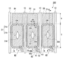
本実施の形態の液晶表示装置100は、図2に示したように、データ線9および走査線13等にて囲まれた領域の内側に画素電極31を備えてなるドット領域を有している。このドット領域内には、図3に示すように、1つのドット領域に対応して3原色のうちの異なる色の1つの着色層が配設され、3つのドット領域(D1,D2,D3)で赤色、緑色、青色を含む1つの画素を形成している。
Next, a pixel configuration of the liquid crystal display device 100 according to the present embodiment will be described with reference to FIGS. FIG. 3 is a schematic diagram illustrating a pixel configuration of the liquid crystal display device 100, particularly a planar configuration of the pixel electrode 31, and FIG. 4 is a schematic diagram illustrating a cross section taken along line AA ′ of FIG. In FIG. 4, the upper side in the drawing is the viewing side.
As shown in FIG. 2, the liquid crystal display device 100 according to the present embodiment has a dot region including a pixel electrode 31 inside a region surrounded by the data lines 9 and the scanning lines 13. . In this dot area, as shown in FIG. 3, one colored layer of different colors among the three primary colors is arranged corresponding to one dot area, and three dot areas (D1, D2, D3) are arranged. Thus, one pixel including red, green, and blue is formed.

ドット領域D1〜D3に設けられた画素電極31は、各ドット領域内に形成されたスリットにより複数(本実施形態では2つ)の島状部(サブピクセル)31a,31bに分割され、各島状部は中央部で連結されている(連結部31c)。各島状部31a,31bはそれぞれサブドット領域S1,S2を構成し、各ドット領域D1,D2,D3はそれぞれ2つのサブドット領域S1,S2に分割された状態となっている。各島状部31a,31bとこれらの島状部を連結する連結部31cはITO(インジウム錫酸化物)等の透明導電膜によって一体に形成されている。図示上側の島状部31aは、各ドット領域内に部分的に設けられた反射膜80の形成領域内に配置されており、残る下側の島状部31bは、反射膜80の非形成領域に配置されている。反射膜80の形成領域内に配置された島状部31aの平面領域が、本液晶表示装置100における反射表示領域Rとされ、残る下側の島状部31bの平面領域が透過表示領域Tとされている。反射膜80の表面には凹凸形状が付与されており、この凹凸によって反射光が散乱されることで、視認性の良い表示が得られるようになっている。すなわち、本実施形態の液晶表示装置100は、1つのドット領域内に反射表示を行なう反射表示領域Rと透過表示を行なう透過表示領域Tとを備えた半透過反射型の液晶表示装置であり、表示可能な領域の略1/3の面積が反射表示に寄与し、残りの略2/3の面積が透過表示に寄与するようになっている。なお、島状部の形状は、図3では正方形状若しくは八角形状であるが、これに限らず、例えば円形状、その他の多角形状のものとすることができる。特に視角特性の均一化の点では、島状部は、その面中心に対して回転対称性を有する形状であることが好ましく、概略円形状又は概略正多角形状の平面形状とすることが好ましい。   The pixel electrodes 31 provided in the dot regions D1 to D3 are divided into a plurality of (two in this embodiment) island-shaped portions (subpixels) 31a and 31b by slits formed in each dot region. The shaped parts are connected at the central part (connecting part 31c). Each of the island portions 31a and 31b constitutes sub-dot regions S1 and S2, and each of the dot regions D1, D2 and D3 is divided into two sub-dot regions S1 and S2. Each island-shaped part 31a, 31b and the connection part 31c which connects these island-shaped parts are integrally formed by transparent conductive films, such as ITO (indium tin oxide). The upper island portion 31a in the drawing is disposed in the formation region of the reflection film 80 partially provided in each dot region, and the remaining lower island portion 31b is the non-formation region of the reflection film 80. Is arranged. The planar region of the island-shaped portion 31a disposed in the formation region of the reflective film 80 is the reflective display region R in the present liquid crystal display device 100, and the remaining planar region of the lower island-shaped portion 31b is the transmissive display region T. Has been. The surface of the reflective film 80 is provided with an uneven shape, and reflected light is scattered by the unevenness, whereby a display with good visibility can be obtained. That is, the liquid crystal display device 100 of the present embodiment is a transflective liquid crystal display device including a reflective display region R that performs reflective display and a transmissive display region T that performs transmissive display in one dot region. Approximately 1/3 of the displayable area contributes to reflective display, and the remaining approximately 2/3 of the area contributes to transmissive display. In addition, although the shape of an island-shaped part is square shape or octagonal shape in FIG. 3, it is not restricted to this, For example, it can be set as a circular shape and another polygonal shape. In particular, from the viewpoint of uniform viewing angle characteristics, the island-shaped portion preferably has a shape having rotational symmetry with respect to the center of the surface, and preferably has a planar shape of a substantially circular shape or a substantially regular polygonal shape.

また本実施形態において、連結部31cの寸法は、前記島状部31a,31bの配列方向(図示上下方向)に延在する縦方向の寸法d1が10μm、前記島状部31a,31bの配列方向に直交する横方向の寸法d2が10μmに設定されている。このような寸法形状とすることで、ディスクリネーションの核を連結部31cに強固に固定することが可能になる。本実施形態のように1ドットを複数のサブドットに分割した場合、これらのサブドットの境界部には、液晶がうまく配向できない部分(ディスクリネーション)が発生する。このディスクリネーションの核は連結部31cの領域に捕捉されるが、この捕捉力が弱いと、中間調等でディスクリネーションの核が移動し、視認性を低下させることがある。本発明者は、連結部31の領域におけるディスクリネーションの捕捉力と連結部31cの寸法との関係を調べ、良好な視認性が得られる寸法範囲を求めた。表1は、連結部31cの寸法d1,d2とディスクリネーションの捕捉力(ディスクリネーションの移動のしやすさ)との関係をまとめたものである。本実施形態では、縦方向の寸法d1及び横方向の寸法d2が共に10μmである場合に反射表示と透過表示の双方で良好な視認性が得られたが、縦方向の寸法d1と横方向の寸法d2が表1の実施例で示す範囲にあれば概ね良好な視認性が得られる。表1によれば、縦方向の寸法d1の下限は7μmから9μmの間(概ね8μm)であり、上限は20μm程度である。また、横方向の寸法d2の下限は5μm程度であり、上限は20μm程度である。すなわち、縦方向の寸法d1が8μm以上20μm以下で且つ横方向の寸法d2が5μm以上20μm以下であれば、概ね良好な視認性が得られる。このため、連結部31cの寸法d1,d2をこの範囲に規定することで、反射表示領域Rに突起等の配向規制手段を設けなくても、配向状態を良好に保つことができるようになる。   In the present embodiment, the connecting portion 31c has a vertical dimension d1 extending in the arrangement direction (vertical direction in the figure) of the island-like portions 31a and 31b of 10 μm, and the arrangement direction of the island-like portions 31a and 31b. The horizontal dimension d2 orthogonal to is set to 10 μm. With such a dimensional shape, the disclination nucleus can be firmly fixed to the connecting portion 31c. When one dot is divided into a plurality of subdots as in the present embodiment, a portion (disclination) where the liquid crystal cannot be well aligned occurs at the boundary between these subdots. The disclination nucleus is captured in the region of the connecting portion 31c. However, if the capturing force is weak, the disclination nucleus may move in a halftone or the like, which may reduce visibility. The inventor investigated the relationship between the disclination capturing force in the region of the connecting portion 31 and the size of the connecting portion 31c, and obtained a size range in which good visibility was obtained. Table 1 summarizes the relationship between the dimensions d1 and d2 of the connecting portion 31c and the disclination capturing force (ease of movement of disclination). In this embodiment, when both the vertical dimension d1 and the horizontal dimension d2 are 10 μm, good visibility is obtained in both the reflective display and the transmissive display. However, the vertical dimension d1 and the horizontal dimension d1 are obtained. If the dimension d2 is within the range shown in the examples of Table 1, generally good visibility can be obtained. According to Table 1, the lower limit of the vertical dimension d1 is between 7 μm and 9 μm (generally 8 μm), and the upper limit is about 20 μm. The lower limit of the horizontal dimension d2 is about 5 μm, and the upper limit is about 20 μm. That is, if the vertical dimension d1 is 8 μm or more and 20 μm or less and the horizontal dimension d2 is 5 μm or more and 20 μm or less, generally good visibility can be obtained. For this reason, by defining the dimensions d1 and d2 of the connecting portion 31c within this range, the alignment state can be maintained well without providing the reflective display region R with alignment regulating means such as protrusions.

Figure 0004506362
Figure 0004506362

TFD素子40は、走査線13と画素電極31とを接続するスイッチング素子であって、走査線13に沿って延びる第1金属膜41と、2つの第2金属膜42,43との間に図示略の絶縁膜を挟んだ構造を有している。走査線13を分岐して形成された第2金属膜42と第1金属膜41との交差部に第1素子部40aが形成され、第1金属膜41と、第2金属膜43との交差部に第2素子部40bが形成されている。そして、第2金属膜43にコンタクトホールCを介して島状部31b(画素電極31)が接続されている。本実施形態に係るTFD素子40は、2つの素子部40a、40bが逆向きに接続された構造を備えているので、印加電圧の極性によらず安定した素子特性を得られるものとなっている。第1金属膜41は例えばTa(タンタル)からなるものとされ、前記絶縁膜は例えばタンタル酸化物からなるものとされる。また、第2金属膜42(走査線13)及び第2金属膜43は、例えばCr(クロム)からなるものとされる。   The TFD element 40 is a switching element that connects the scanning line 13 and the pixel electrode 31, and is illustrated between the first metal film 41 extending along the scanning line 13 and the two second metal films 42 and 43. It has a structure in which a substantially insulating film is sandwiched. A first element portion 40 a is formed at the intersection of the second metal film 42 formed by branching the scanning line 13 and the first metal film 41, and the intersection of the first metal film 41 and the second metal film 43. The second element part 40b is formed in the part. The island portion 31b (pixel electrode 31) is connected to the second metal film 43 through the contact hole C. Since the TFD element 40 according to the present embodiment has a structure in which the two element portions 40a and 40b are connected in opposite directions, stable element characteristics can be obtained regardless of the polarity of the applied voltage. . The first metal film 41 is made of, for example, Ta (tantalum), and the insulating film is made of, for example, tantalum oxide. The second metal film 42 (scanning line 13) and the second metal film 43 are made of, for example, Cr (chromium).

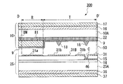
次に、図4に示す断面構造をみると、液晶表示装置100は、素子基板10とこれに対向配置された対向基板25とを備え、これらの基板の間に初期配向状態が垂直配向状態を呈する誘電率異方性が負の液晶からなる液晶層50が挟持されている。対向基板10の外面側にあたる液晶セルの外側には、照明手段として光源、リフレクタ、導光板などを有するバックライト(図示略)が設置されている。   Next, referring to the cross-sectional structure shown in FIG. 4, the liquid crystal display device 100 includes an element substrate 10 and a counter substrate 25 disposed so as to face the element substrate 10, and an initial alignment state between these substrates is a vertical alignment state. A liquid crystal layer 50 made of liquid crystal having negative dielectric anisotropy is sandwiched. A backlight (not shown) having a light source, a reflector, a light guide plate, and the like is provided as illumination means outside the liquid crystal cell corresponding to the outer surface side of the counter substrate 10.

素子基板25は、石英、ガラス等の透光性材料からなる基板本体25Aを基体としてなり、基板本体25Aの内面側に走査線13やTFD素子40等(図3参照)を備えている。そして、走査線13等を覆って層間絶縁膜15が形成され、この層間絶縁膜15上に画素電極31が形成されている。層間絶縁膜15には、コンタクトホールC(図3参照)が形成されており、このコンタクトホールをCを介してTFD素子40と島状部31b(画素電極31)とが電気的に接続されている。また図示は省略したが、画素電極31及び層間絶縁膜15を覆ってポリイミド等の垂直配向膜が形成されており、液晶分子の初期配向を基板面に対し垂直に配向させるようになっている。基板本体25Aの外面側には、位相差板36、偏光板37が順に積層されている。尚、図3に示したTFD素子40は、層間絶縁膜15と基板本体25Aとの間に設けられている。   The element substrate 25 has a substrate body 25A made of a translucent material such as quartz or glass as a base, and includes a scanning line 13, a TFD element 40, and the like (see FIG. 3) on the inner surface side of the substrate body 25A. An interlayer insulating film 15 is formed so as to cover the scanning lines 13 and the like, and a pixel electrode 31 is formed on the interlayer insulating film 15. A contact hole C (see FIG. 3) is formed in the interlayer insulating film 15, and the TFD element 40 and the island-shaped portion 31b (pixel electrode 31) are electrically connected through the contact hole C. Yes. Although not shown, a vertical alignment film such as polyimide is formed so as to cover the pixel electrode 31 and the interlayer insulating film 15, and the initial alignment of the liquid crystal molecules is aligned perpendicular to the substrate surface. A phase difference plate 36 and a polarizing plate 37 are sequentially stacked on the outer surface side of the substrate body 25A. The TFD element 40 shown in FIG. 3 is provided between the interlayer insulating film 15 and the substrate body 25A.

対向基板10は、石英、ガラス等の透光性材料からなる基板本体10Aを基体としてなり、基板本体10Aの内面側には、Al(アルミニウム)やAg(銀)等の反射率の高い金属膜からなる反射膜80が図示略の絶縁膜を介して部分的に形成されている。この絶縁膜は、その表面に凹凸形状を備えており、係る凹凸形状に倣って反射膜80の表面は凹凸部を有する。このような凹凸により反射光が散乱されるため、反射表示の視野角特性が向上し、良好な視認性を得ることができる。ドット領域内の反射膜80上、及び基板本体10A上には、反射表示領域R及び透過表示領域Tに跨ってカラーフィルタ(カラーフィルタ層)22が設けられている。カラーフィルタ22は互いに色の異なる複数種類のカラーフィルタ(着色層)からなり、これらカラーフィルタ層22を構成する各カラーフィルタの間には必要に応じて黒色樹脂等からなる遮光層BM(ブラックマトリクス)が配置される。   The counter substrate 10 has a substrate body 10A made of a translucent material such as quartz or glass as a base, and a metal film having a high reflectance such as Al (aluminum) or Ag (silver) is formed on the inner surface side of the substrate body 10A. A reflective film 80 made of is partially formed through an insulating film (not shown). This insulating film has an uneven shape on its surface, and the surface of the reflective film 80 has an uneven portion following the uneven shape. Since the reflected light is scattered by such irregularities, the viewing angle characteristics of the reflective display are improved, and good visibility can be obtained. A color filter (color filter layer) 22 is provided across the reflective display region R and the transmissive display region T on the reflective film 80 in the dot region and on the substrate body 10A. The color filter 22 is composed of a plurality of types of color filters (colored layers) having different colors, and a light shielding layer BM (black matrix) made of black resin or the like between the color filters constituting the color filter layer 22 as necessary. ) Is arranged.

カラーフィルタ22の内面側には反射表示領域Rに対応して絶縁膜81が選択的に形成されている。このようにドット領域内に部分的に形成された絶縁膜81により、液晶層50の層厚が反射表示領域Rと透過表示領域Tとで異ならされている。絶縁膜81は、アクリル樹脂等の有機材料膜を用いて形成されている。絶縁膜81は、例えば膜厚が2μm±1μm程度に形成され、絶縁膜81が存在しない部分の液晶層50の厚みは2μm〜6μm程度であり、反射表示領域Rにおける液晶層50の厚みは透過表示領域Tにおける液晶層50の厚みの約半分となっている。つまり、絶縁膜81は、自身の膜厚によって反射表示領域Rと透過表示領域Tとにおける液晶層50の層厚を異ならせる液晶層厚調整層として機能し、もってマルチギャップ構造を実現するものとなっている。本例の液晶表示装置100は、係る構成により明るく高コントラストの表示が得られるようになっている。   An insulating film 81 is selectively formed on the inner surface side of the color filter 22 corresponding to the reflective display region R. As described above, the insulating film 81 partially formed in the dot region makes the thickness of the liquid crystal layer 50 different between the reflective display region R and the transmissive display region T. The insulating film 81 is formed using an organic material film such as an acrylic resin. The insulating film 81 is formed to have a thickness of, for example, about 2 μm ± 1 μm. The thickness of the liquid crystal layer 50 where the insulating film 81 does not exist is about 2 μm to 6 μm, and the thickness of the liquid crystal layer 50 in the reflective display region R is transmissive. This is about half the thickness of the liquid crystal layer 50 in the display region T. That is, the insulating film 81 functions as a liquid crystal layer thickness adjusting layer that varies the thickness of the liquid crystal layer 50 in the reflective display region R and the transmissive display region T according to its own film thickness, thereby realizing a multi-gap structure. It has become. The liquid crystal display device 100 of the present example can display a bright and high-contrast display with such a configuration.

さらに基板本体25Aの内面側には、カラーフィルタ22と絶縁膜81の表面を覆って対向電極9が形成されている。対向電極9はITO等からなるストライプ状の透明導電膜であり、この対向電極9において島状部31bの中央部に対向する位置には、平面視六角形状の開口部(電極スリット)9Aが設けられている。この開口部9Aは電圧印加時の液晶分子の傾倒方向を制御するための配向規制手段として機能するものである。このように対向電極9に開口部9Aを設けると、開口部9Aの周辺では、開口部9Aから該開口部9Aに対向する島状部31bの周縁に沿って斜め電界が生じる。このため、液晶分子51は、図3に示すように、開口部9Aを中心として放射状に倒れ、それを中心とした平面放射状に液晶分子51が配向する。従って、本実施形態の液晶表示装置100では、電圧印加時に液晶分子51のダイレクタが全方位に向くこととなり、視野角の極めて広い表示が実現されるようになる。また図示は省略したが、対向電極9及びカラーフィルタ22を覆って垂直配向膜が形成されており、液晶分子51の初期配向を基板面に対し垂直に配向させるようになっている。基板本体10Aの外面側には、位相差板16と偏光板17とが積層配置されている。   Further, the counter electrode 9 is formed on the inner surface side of the substrate body 25 </ b> A so as to cover the surfaces of the color filter 22 and the insulating film 81. The counter electrode 9 is a striped transparent conductive film made of ITO or the like, and an opening (electrode slit) 9A having a hexagonal shape in a plan view is provided at a position facing the central portion of the island portion 31b in the counter electrode 9. It has been. The opening 9A functions as an alignment regulating means for controlling the tilt direction of the liquid crystal molecules when a voltage is applied. When the opening 9A is provided in the counter electrode 9 in this manner, an oblique electric field is generated around the opening 9A along the periphery of the island-shaped portion 31b facing the opening 9A from the opening 9A. Therefore, as shown in FIG. 3, the liquid crystal molecules 51 fall radially about the opening 9 </ b> A, and the liquid crystal molecules 51 are aligned radially around the center. Therefore, in the liquid crystal display device 100 of the present embodiment, the director of the liquid crystal molecules 51 faces in all directions when a voltage is applied, and a display with a very wide viewing angle is realized. Although not shown, a vertical alignment film is formed so as to cover the counter electrode 9 and the color filter 22, and the initial alignment of the liquid crystal molecules 51 is aligned perpendicular to the substrate surface. A phase difference plate 16 and a polarizing plate 17 are laminated on the outer surface side of the substrate body 10A.

以上説明したように、本実施形態の液晶表示装置100によれば、ドット領域内に部分的に液晶層厚調整用の絶縁膜81を設けたマルチギャップ構造を採用しているので、透過表示領域Tと反射表示領域Rとで液晶層50のリタデーションを揃えることができ、透過表示、反射表示のいずれにおいても高コントラストの表示が得られる。また、画素電極31が複数の島状部31a,31bに分割されるとともに、島状部31bの中央部に対応して電極スリット9Aが設けられているので、電圧印加時には液晶分子51が画像表示領域内で電極スリット9Aを中心に放射状に配向されるようになり、広視野角な表示が実現される。また本実施形態では、連結部31cの寸法形状が前述のように規定されているので、ディスクリネーションの核は連結部31c上に固定され、移動することはない。このため、前記核が移動することによって生じるざらざらとした表示不良が改善され、視認性の良い反射表示が得られるようになる。この構成では、反射表示領域には突起等の構造物が配置されないので、その分表示面積が広がり、明るい反射表示を得ることができる。   As described above, according to the liquid crystal display device 100 of the present embodiment, since the multi-gap structure in which the insulating film 81 for adjusting the liquid crystal layer thickness is partially provided in the dot area is employed, the transmissive display area The retardation of the liquid crystal layer 50 can be made uniform between T and the reflective display region R, and high contrast display can be obtained in both transmissive display and reflective display. Further, the pixel electrode 31 is divided into a plurality of island-shaped portions 31a and 31b, and the electrode slit 9A is provided corresponding to the central portion of the island-shaped portion 31b. In the region, the electrodes are radially oriented around the electrode slit 9A, and a display with a wide viewing angle is realized. In the present embodiment, since the dimensional shape of the connecting portion 31c is defined as described above, the core of the disclination is fixed on the connecting portion 31c and does not move. For this reason, the rough display defect which arises when the said nucleus moves is improved, and a reflective display with sufficient visibility comes to be obtained. In this configuration, since structures such as protrusions are not arranged in the reflective display area, the display area is increased correspondingly and a bright reflective display can be obtained.

[第2の実施の形態]
以下、本発明の第2の実施の形態を図5、図6を参照しつつ説明する。
図5は、本実施の形態の液晶表示装置について1つの画素の平面図を示すものであり、第1の実施の形態の図3に相当する模式図である。図6は図5のB−B‘断面を示す模式図であり、第1の実施の形態の図4に相当する図である。なお、図6では図示上側が視認側とされる。本実施の形態の液晶表示装置の基本構成は第1の実施の形態と同様であり、異なる点は、画素電極が島状部に分割されない点と、反射表示領域内の画素電極が光反射性の導電材料によって形成されている点と、透過表示領域の配向規制手段が突起と電極スリットによって構成されている点のみである。したがって、図5、図6において図3、図4と共通の構成要素には同一の符号を付し、詳細な説明は省略する。
[Second Embodiment]
Hereinafter, a second embodiment of the present invention will be described with reference to FIGS.
FIG. 5 shows a plan view of one pixel in the liquid crystal display device of the present embodiment, and is a schematic view corresponding to FIG. 3 of the first embodiment. FIG. 6 is a schematic diagram showing a BB ′ cross section of FIG. 5 and corresponds to FIG. 4 of the first embodiment. In FIG. 6, the upper side in the drawing is the viewing side. The basic configuration of the liquid crystal display device of this embodiment is the same as that of the first embodiment, except that the pixel electrode is not divided into island-shaped portions and the pixel electrode in the reflective display region is light reflective. These are only the point formed by the conductive material and the point that the orientation regulating means of the transmissive display region is constituted by the protrusion and the electrode slit. Therefore, in FIGS. 5 and 6, the same components as those in FIGS. 3 and 4 are denoted by the same reference numerals, and detailed description thereof is omitted.

図5に示すように、本実施形態においてドット領域D1〜D3に設けられた画素電極31は、反射表示領域Rと透過表示領域Tに跨る略矩形状の電極として構成されている。この画素電極31のうち図示上側の電極部31aはAl(アルミニウム)やAg(銀)等の光反射性の金属膜若しくはこれらの金属膜とITO(インジウム錫酸化物)等の透明導電膜との積層膜からなる。この電極部31aは反射電極として機能し、この電極部31aの形成された領域が反射表示領域Rとなる。電極部31aの表面には凹凸形状が付与されており、この凹凸によって反射光が散乱されることで、視認性の良い表示が得られるようになっている。また、図示下側の電極部31bはITO(インジウム錫酸化物)等の透明導電膜からなり、この電極部31bの形成された領域が透過表示領域Tとなる。すなわち、本実施形態の液晶表示装置200は、1つのドット領域内に反射表示を行なう反射表示領域Rと透過表示を行なう透過表示領域Tとを備えた半透過反射型の液晶表示装置であり、表示可能な領域の略1/3の面積が反射表示に寄与し、残りの略2/3の面積が透過表示に寄与するようになっている。   As shown in FIG. 5, the pixel electrodes 31 provided in the dot regions D <b> 1 to D <b> 3 in the present embodiment are configured as substantially rectangular electrodes that straddle the reflective display region R and the transmissive display region T. Of the pixel electrode 31, an upper electrode portion 31 a in the drawing is formed of a light reflective metal film such as Al (aluminum) or Ag (silver) or a transparent conductive film such as ITO (indium tin oxide). It consists of a laminated film. The electrode portion 31a functions as a reflective electrode, and a region where the electrode portion 31a is formed becomes a reflective display region R. The surface of the electrode portion 31a is provided with a concavo-convex shape, and the reflected light is scattered by the concavo-convex, whereby a display with good visibility can be obtained. Further, the lower electrode portion 31b is made of a transparent conductive film such as ITO (indium tin oxide), and a region where the electrode portion 31b is formed becomes a transmissive display region T. That is, the liquid crystal display device 200 of the present embodiment is a transflective liquid crystal display device including a reflective display region R that performs reflective display and a transmissive display region T that performs transmissive display within one dot region. Approximately 1/3 of the displayable area contributes to reflective display, and the remaining approximately 2/3 of the area contributes to transmissive display.

各画素電極31には、透過表示領域Tの中央部となる位置に開口部(電極スリット)31Aが設けられており、更に、この画素電極31と液晶層を挟んで対向する対向基板側には、誘電体からなる突起18が透過表示領域Tの縁辺に沿って環状に設けられている。この突起18と電極スリット31Aは電圧印加時の液晶分子の傾倒方向を制御するための配向規制手段として機能するものである。このように画素電極31に開口部31Aを設けた場合、開口部31Aの周辺では該開口部31Aの辺端に垂直に斜め電界が発生し、液晶分子51は開口部31Aの輪郭に対して垂直方向に傾倒する。また突起18の周辺では、電圧無印加時には液晶分子51が突起18の傾斜面と垂直に配向し、電圧印加時には突起18から外側に向かって液晶分子51が倒れ、それを中心とした平面放射状に液晶分子51が配向する。従って、透過表示領域Tでは、電圧印加時に液晶分子51のダイレクタが全方位に向くこととなり、視野角の極めて広い表示が実現される。さらに、突起18が反射表示領域Rの境界部にも配置されているので、突起18による配向規制力を反射表示領域Rにまで大きく及ぼすことができる。   Each pixel electrode 31 is provided with an opening (electrode slit) 31A at a position that is the central portion of the transmissive display region T, and on the opposite substrate side facing the pixel electrode 31 with the liquid crystal layer interposed therebetween. The protrusion 18 made of a dielectric is provided in an annular shape along the edge of the transmissive display region T. The protrusions 18 and the electrode slits 31A function as alignment regulating means for controlling the tilting direction of the liquid crystal molecules when a voltage is applied. When the opening 31A is provided in the pixel electrode 31 in this manner, an oblique electric field is generated perpendicular to the edge of the opening 31A around the opening 31A, and the liquid crystal molecules 51 are perpendicular to the outline of the opening 31A. Tilt in the direction. In the vicinity of the protrusion 18, the liquid crystal molecules 51 are aligned perpendicularly to the inclined surface of the protrusion 18 when no voltage is applied, and the liquid crystal molecules 51 are tilted outward from the protrusion 18 when a voltage is applied. The liquid crystal molecules 51 are aligned. Therefore, in the transmissive display region T, the director of the liquid crystal molecules 51 is directed in all directions when a voltage is applied, and a display with a very wide viewing angle is realized. Furthermore, since the protrusion 18 is also arranged at the boundary portion of the reflective display region R, the alignment regulating force by the protrusion 18 can be greatly exerted on the reflective display region R.

突起18は、反射表示領域Rと透過表示領域Tとの境界部に切れ目18Aを有する開環状に形成されており、突起18の寸法は、前記突起18の幅d3(前記電極部31a,31bの配列方向に延在する切れ目18Aの縦方向の寸法)が10μm、前記切れ目18Aの幅d4(前記電極部31a,31bの配列方向に直交する横方向の寸法)が12μmに設定されている。このような寸法形状とすることで、ディスクリネーションの核を該突起18の切れ目18Aの部分に強固に固定することが可能になる。本実施形態のように透過表示領域Tの周りに突起を設けて配向制御をする場合、透過表示領域Tと反射表示領域Rとの境界部には、液晶がうまく配向できない部分(ディスクリネーション)が発生する。
このディスクリネーションの核は突起18の切れ目18Aの領域に捕捉されるが、この捕捉力が弱いと、中間調等でディスクリネーションの核が移動し、視認性を低下させることがある。本発明者は、切れ目18Aの領域におけるディスクリネーションの捕捉力と切れ目18Aの寸法d3,d4との関係を調べ、良好な視認性が得られる寸法範囲を求めた。
表2は、切れ目18Aの寸法d3,d4とディスクリネーションの捕捉力(ディスクリネーションの移動のしやすさ)との関係をまとめたものである。本実施形態では、縦方向の寸法d3が10μm、横方向の寸法d4が12μmである場合に反射表示と透過表示の双方で良好な視認性が得られたが、縦方向の寸法d3と横方向の寸法d4が表2の実施例で示す範囲にあれば概ね良好な視認性が得られる。表2によれば、縦方向の寸法d3の下限は7μmから10μmの間(概ね8μm)であり、上限は20μm程度である。また、横方向の寸法d4の下限は5μm程度であり、上限は20μm程度である。すなわち、縦方向の寸法d3が8μm以上20μm以下で且つ横方向の寸法4が5μm以上20μm以下であれば、概ね良好な視認性が得られる。このため、突起18の寸法d3,d4をこの範囲に規定することで、反射表示領域Rに突起等の配向規制手段を設けなくても、配向状態を良好に保つことができるようになる。
The protrusion 18 is formed in an open ring shape having a cut 18A at the boundary between the reflective display region R and the transmissive display region T, and the dimension of the protrusion 18 is the width d3 of the protrusion 18 (of the electrode portions 31a and 31b). The vertical dimension of the cut line 18A extending in the arrangement direction is set to 10 μm, and the width d4 of the cut line 18A (the horizontal dimension orthogonal to the arrangement direction of the electrode portions 31a and 31b) is set to 12 μm. By adopting such a dimensional shape, it becomes possible to firmly fix the disclination nucleus to the cut portion 18A of the projection 18. When alignment is controlled by providing protrusions around the transmissive display region T as in the present embodiment, a portion where the liquid crystal cannot be aligned well (disclination) at the boundary between the transmissive display region T and the reflective display region R Will occur.
The disclination nucleus is captured in the region of the cut 18A of the protrusion 18. However, if the capturing force is weak, the disclination nucleus may move in a halftone or the like, which may reduce visibility. The inventor investigated the relationship between the disclination capturing force in the region of the cut 18A and the dimensions d3 and d4 of the cut 18A, and obtained a size range in which good visibility can be obtained.
Table 2 summarizes the relationship between the dimensions d3 and d4 of the cut 18A and the disclination capturing force (ease of movement of disclination). In this embodiment, when the dimension d3 in the vertical direction is 10 μm and the dimension d4 in the horizontal direction is 12 μm, good visibility is obtained in both the reflective display and the transmissive display. If the dimension d4 is within the range shown in the examples of Table 2, generally good visibility can be obtained. According to Table 2, the lower limit of the vertical dimension d3 is between 7 μm and 10 μm (generally 8 μm), and the upper limit is about 20 μm. The lower limit of the horizontal dimension d4 is about 5 μm, and the upper limit is about 20 μm. That is, if the vertical dimension d3 is 8 μm or more and 20 μm or less and the horizontal dimension d4 is 5 μm or more and 20 μm or less, generally good visibility can be obtained. For this reason, by defining the dimensions d3 and d4 of the protrusions 18 within this range, the alignment state can be maintained satisfactorily without providing an alignment regulating means such as protrusions in the reflective display region R.

Figure 0004506362
Figure 0004506362

次に、図6に示す断面構造をみると、液晶表示装置200は、素子基板25とこれに対向配置された対向基板10とを備え、これらの基板の間に初期配向状態が垂直配向状態を呈する誘電率異方性が負の液晶からなる液晶層50が挟持されている。素子基板25の外面側にあたる液晶セルの外側には、照明手段として光源、リフレクタ、導光板などを有するバックライト(図示略)が設置されている。 Next, referring to the cross-sectional structure shown in FIG. 6, the liquid crystal display device 200 includes an element substrate 25 and a counter substrate 10 disposed to face the element substrate 25, and an initial alignment state between these substrates is a vertical alignment state. A liquid crystal layer 50 made of liquid crystal having negative dielectric anisotropy is sandwiched. A backlight (not shown) having a light source, a reflector, a light guide plate, and the like is provided as illumination means outside the liquid crystal cell corresponding to the outer surface side of the element substrate 25.

素子基板25は、石英、ガラス等の透光性材料からなる基板本体25Aを基体としてなり、基板本体25Aの内面側に走査線13やTFD素子40等(図5参照)を備えている。そして、走査線13等を覆って層間絶縁膜15が形成され、この層間絶縁膜15上に画素電極31が形成されている。この画素電極31は反射表示領域Rに設けられた光反射性の電極部31aと透過表示領域Tに設けられた透光性の電極部31bによって構成されている。透過表示領域Tに配置された電極部31bには、中央部に開口部31Aが設けられており、この開口部31Aの辺端に生じる斜め電界の作用によって液晶の傾倒方向を制御できるようになっている。層間絶縁膜15には、突起18に対向する位置にコンタクトホールC(図5参照)が形成されており、このコンタクトホールをCを介してTFD素子40と電極部31b(画素電極31)とが電気的に接続されている。また図示は省略したが、画素電極31及び層間絶縁膜15を覆ってポリイミド等の垂直配向膜が形成されており、液晶分子の初期配向を基板面に対し垂直に配向させるようになっている。基板本体25Aの外面側には、位相差板36、偏光板37が順に積層されている。尚、図5に示したTFD素子40は、層間絶縁膜15と基板本体25Aとの間に設けられている。   The element substrate 25 has a substrate body 25A made of a translucent material such as quartz or glass as a base, and includes a scanning line 13, a TFD element 40, and the like (see FIG. 5) on the inner surface side of the substrate body 25A. An interlayer insulating film 15 is formed so as to cover the scanning lines 13 and the like, and a pixel electrode 31 is formed on the interlayer insulating film 15. The pixel electrode 31 includes a light reflective electrode portion 31 a provided in the reflective display region R and a light transparent electrode portion 31 b provided in the transmissive display region T. The electrode portion 31b disposed in the transmissive display region T is provided with an opening 31A at the center, and the tilt direction of the liquid crystal can be controlled by the action of an oblique electric field generated at the edge of the opening 31A. ing. A contact hole C (see FIG. 5) is formed in the interlayer insulating film 15 at a position facing the protrusion 18, and the TFD element 40 and the electrode portion 31 b (pixel electrode 31) are connected through the contact hole C. Electrically connected. Although not shown, a vertical alignment film such as polyimide is formed so as to cover the pixel electrode 31 and the interlayer insulating film 15, and the initial alignment of the liquid crystal molecules is aligned perpendicular to the substrate surface. A phase difference plate 36 and a polarizing plate 37 are sequentially stacked on the outer surface side of the substrate body 25A. 5 is provided between the interlayer insulating film 15 and the substrate body 25A.

対向基板10は、石英、ガラス等の透光性材料からなる基板本体10Aを基体としてなり、基板本体10Aの内面側には、反射表示領域R及び透過表示領域Tに跨ってカラーフィルタ(カラーフィルタ層)22が設けられている。カラーフィルタ22は互いに色の異なる複数種類のカラーフィルタ(着色層)からなり、これらカラーフィルタ層22を構成する各カラーフィルタの間には必要に応じて黒色樹脂等からなる遮光層BM(ブラックマトリクス)が配置される。カラーフィルタ22の内面側には反射表示領域Rに対応して絶縁膜81が選択的に形成されている。このようにドット領域内に部分的に形成された絶縁膜81により、液晶層50の層厚が反射表示領域Rと透過表示領域Tとで異ならされている。絶縁膜81は、アクリル樹脂等の有機材料膜を用いて形成されている。絶縁膜81は、例えば膜厚が2μm±1μm程度に形成され、絶縁膜81が存在しない部分の液晶層50の厚みは2μm〜6μm程度であり、反射表示領域Rにおける液晶層50の厚みは透過表示領域Tにおける液晶層50の厚みの約半分となっている。つまり、絶縁膜81は、自身の膜厚によって反射表示領域Rと透過表示領域Tとにおける液晶層50の層厚を異ならせる液晶層厚調整層として機能し、もってマルチギャップ構造を実現するものとなっている。本例の液晶表示装置200は、係る構成により明るく高コントラストの表示が得られるようになっている。   The counter substrate 10 has a substrate body 10A made of a translucent material such as quartz or glass as a base, and a color filter (color filter) is formed on the inner surface side of the substrate body 10A across the reflective display region R and the transmissive display region T. Layer) 22 is provided. The color filter 22 is composed of a plurality of types of color filters (colored layers) having different colors, and a light shielding layer BM (black matrix) made of black resin or the like between the color filters constituting the color filter layer 22 as necessary. ) Is arranged. An insulating film 81 is selectively formed on the inner surface side of the color filter 22 corresponding to the reflective display region R. As described above, the insulating film 81 partially formed in the dot region makes the thickness of the liquid crystal layer 50 different between the reflective display region R and the transmissive display region T. The insulating film 81 is formed using an organic material film such as an acrylic resin. The insulating film 81 is formed to have a thickness of, for example, about 2 μm ± 1 μm. The thickness of the liquid crystal layer 50 where the insulating film 81 does not exist is about 2 μm to 6 μm, and the thickness of the liquid crystal layer 50 in the reflective display region R is transmissive. This is about half the thickness of the liquid crystal layer 50 in the display region T. That is, the insulating film 81 functions as a liquid crystal layer thickness adjusting layer that varies the thickness of the liquid crystal layer 50 in the reflective display region R and the transmissive display region T according to its own film thickness, thereby realizing a multi-gap structure. It has become. The liquid crystal display device 200 of this example is configured so that a bright and high-contrast display can be obtained.

さらに基板本体10Aの内面側には、カラーフィルタ22と絶縁膜81の表面を覆って対向電極9が形成されている。対向電極9はITO等からなるストライプ状の透明導電膜であり、この対向電極9の上には、透過表示領域Tの縁辺に沿って誘電体からなる環状の突起18が配設されている。前述のように、この突起18は素子基板側の電極スリット31Aと共に透過表示領域Tの配向制御を行なう配向規制手段を構成するものである。また、反射表示領域Rとの境界部に配した突起18によって、この配向規制力を反射表示領域Rにまで及ぼすことが可能となっている。また突起18には、反射表示領域Rと透過表示領域Tとの境界部に前述の寸法を有する切れ目18A(図5参照)が設けられており、この切れ目18Aが形成された領域にディスクリネーションの核を固定できるようになっている。また図示は省略したが、対向電極9及びカラーフィルタ22を覆って垂直配向膜が形成されており、液晶分子51の初期配向を基板面に対し垂直に配向させるようになっている。基板本体10Aの外面側には、位相差板16と偏光板17とが積層配置されている。 Further, the counter electrode 9 is formed on the inner surface side of the substrate body 10 </ b> A so as to cover the surfaces of the color filter 22 and the insulating film 81. The counter electrode 9 is a striped transparent conductive film made of ITO or the like, and an annular protrusion 18 made of a dielectric material is disposed on the counter electrode 9 along the edge of the transmissive display region T. As described above, the protrusion 18 constitutes an alignment regulating means for controlling the alignment of the transmissive display region T together with the electrode slit 31A on the element substrate side. Further, this alignment regulating force can be applied to the reflective display region R by the protrusions 18 arranged at the boundary with the reflective display region R. Further, the protrusion 18 is provided with a cut 18A (see FIG. 5) having the above-described dimensions at the boundary between the reflective display region R and the transmissive display region T, and the disclination is formed in the region where the cut 18A is formed. Can be fixed. Although not shown, a vertical alignment film is formed so as to cover the counter electrode 9 and the color filter 22, and the initial alignment of the liquid crystal molecules 51 is aligned perpendicular to the substrate surface. A phase difference plate 16 and a polarizing plate 17 are laminated on the outer surface side of the substrate body 10A.

以上説明したように、本実施形態でもマルチギャップ構造を採用しているので、反射表示と透過表示の双方において高コントラストな表示を得ることができる。また本実施形態では、反射表示領域Rと透過表示領域Tの境界部に設けた突起18の切れ目18Aの寸法形状が前述のように規定されているので、ディスクリネーションの核はこの切れ目18Aの形成領域に固定され、移動することはない。このため、前記核が移動することによって生じるざらざらとした表示不良が改善され、視認性の良い反射表示が得られるようになる。この構成では、反射表示領域には突起等の構造物が配置されないので、その分表示面積が広がり、明るい反射表示を得ることができる。また本実施形態では、突起18とコンタクトホールCとが平面的に重なるように配置されているので、コンタクトホール部分で生じるディスクリネーション起因の光漏れを遮断することができる。   As described above, since the multi-gap structure is also adopted in this embodiment, a high-contrast display can be obtained in both the reflective display and the transmissive display. In the present embodiment, since the size and shape of the cut 18A of the projection 18 provided at the boundary between the reflective display region R and the transmissive display region T are defined as described above, the core of the disclination is the boundary of the cut 18A. It is fixed to the formation area and does not move. For this reason, the rough display defect which arises when the said nucleus moves is improved, and a reflective display with sufficient visibility comes to be obtained. In this configuration, since structures such as protrusions are not arranged in the reflective display area, the display area is increased correspondingly and a bright reflective display can be obtained. Further, in the present embodiment, the protrusion 18 and the contact hole C are arranged so as to overlap in a planar manner, so that light leakage caused by disclination occurring in the contact hole portion can be blocked.

[第3の実施の形態]
以下、本発明の第3の実施の形態を図7、図8を参照しつつ説明する。
図7は、本実施の形態の液晶表示装置について1つの画素の平面図を示すものであり、第1の実施の形態の図3に相当する模式図である。図8は図7のD−D‘断面を示す模式図であり、第1の実施の形態の図4に相当する図である。なお、図8では図示上側が視認側とされる。本実施の形態の液晶表示装置の基本構成は第1の実施の形態と同様であり、島状部を連結する連結部の数と、画素電極とTFD素子を接続するコンタクトホールの位置が異なるのみである。したがって、図7、図8において図3、図4と共通の構成要素には同一の符号を付し、詳細な説明は省略する。
[Third Embodiment]
Hereinafter, a third embodiment of the present invention will be described with reference to FIGS.
FIG. 7 shows a plan view of one pixel in the liquid crystal display device of the present embodiment, and is a schematic view corresponding to FIG. 3 of the first embodiment. FIG. 8 is a schematic diagram showing a cross section along DD ′ of FIG. 7 and corresponds to FIG. 4 of the first embodiment. In FIG. 8, the upper side in the drawing is the viewing side. The basic configuration of the liquid crystal display device of this embodiment is the same as that of the first embodiment, except that the number of connecting portions connecting island-like portions and the positions of contact holes connecting pixel electrodes and TFD elements are different. It is. Therefore, in FIG. 7 and FIG. 8, the same reference numerals are given to the same components as those in FIG. 3 and FIG.

図7に示すように、本実施形態においてドット領域D1〜D3に設けられた画素電極31は、各ドット領域内に形成されたスリット(開口部31B)により、略同じ大きさ,形状を有する複数(本実施形態では3つ)の島状部(サブピクセル)31a,31b,31bに分割され、各島状部は中央部で連結されている(連結部31c)。各島状部31a,31b,31bはそれぞれサブドット領域S1,S2,S3を構成し、各ドット領域D1,D2,D3はそれぞれ3つのサブドット領域S1,S2,S3に分割された状態となっている。各島状部31a,31b,31bとこれらの島状部を連結する連結部31cはITO(インジウム錫酸化物)等の透明導電膜によって一体に形成されている。図示上側の島状部31aは、各ドット領域内に部分的に設けられた反射膜80の形成領域内に配置されており、残る下側の島状部31b,31bは、反射膜80の非形成領域に配置されている。反射膜80の形成領域内に配置された島状部31aの平面領域が、本液晶表示装置100における反射表示領域Rとされ、残る下側の島状部31b,31bの平面領域が透過表示領域Tとされている。反射膜80の表面には凹凸形状が付与されており、この凹凸によって反射光が散乱されることで、視認性の良い表示が得られるようになっている。すなわち、本実施形態の液晶表示装置300は、1つのドット領域内に反射表示を行なう反射表示領域Rと透過表示を行なう透過表示領域Tとを備えた半透過反射型の液晶表示装置であり、表示可能な領域の略1/3の面積が反射表示に寄与し、残りの略2/3の面積が透過表示に寄与するようになっている。   As shown in FIG. 7, the pixel electrodes 31 provided in the dot regions D1 to D3 in the present embodiment have a plurality of substantially the same size and shape due to the slits (openings 31B) formed in each dot region. It is divided into (in this embodiment, three) island-shaped portions (sub-pixels) 31a, 31b, 31b, and each island-shaped portion is connected at the central portion (connecting portion 31c). Each of the island portions 31a, 31b, and 31b constitute sub-dot regions S1, S2, and S3, and each of the dot regions D1, D2, and D3 is divided into three sub-dot regions S1, S2, and S3. ing. Each island-shaped part 31a, 31b, 31b and the connection part 31c which connects these island-shaped parts are integrally formed by transparent conductive films, such as ITO (indium tin oxide). The upper island portions 31a in the drawing are arranged in the formation region of the reflective film 80 partially provided in each dot region, and the remaining lower island portions 31b and 31b are non-reflective of the reflective film 80. Arranged in the formation area. The planar area of the island-shaped portion 31a arranged in the formation area of the reflective film 80 is the reflective display area R in the present liquid crystal display device 100, and the remaining planar areas of the lower island-shaped sections 31b and 31b are transmissive display areas. T. The surface of the reflective film 80 is provided with an uneven shape, and reflected light is scattered by the unevenness, whereby a display with good visibility can be obtained. That is, the liquid crystal display device 300 of the present embodiment is a transflective liquid crystal display device including a reflective display region R that performs reflective display and a transmissive display region T that performs transmissive display within one dot region. Approximately 1/3 of the displayable area contributes to reflective display, and the remaining approximately 2/3 of the area contributes to transmissive display.

また本実施形態において、隣接する島状部と島状部との間には連結部31cがそれぞれ複数設けられており、これら複数の連結部31cは、前記隣接する島状部と島状部との中心部を結ぶ線に対して互いに対称となるように配置されている。図7の例では、連結部31cはそれぞれ島状部の左右両端に1つずつ、計2つ設けられている。連結部31cの寸法は、前記島状部の配列方向(図示上下方向)に延在する縦方向の寸法d1が10μm、前記島状部の配列方向に直交する横方向の寸法d2が10μmに設定されている。このような寸法形状とすることで、ディスクリネーションの核を連結部31cに強固に固定することが可能になる(表1参照)。なお、連結部31cの寸法形状は、これに限定されない。縦方向の寸法d1が8μm以上20μm以下で且つ横方向の寸法d2が5μm以上20μm以下であれば、ディスクリネーションの核を強固に固定することができ、良好な視認性が得られるようになる。   In the present embodiment, a plurality of connecting portions 31c are provided between adjacent island portions, and the plurality of connecting portions 31c include the adjacent island portions and the island portions. Are arranged so as to be symmetric with respect to a line connecting the central portions of the two. In the example of FIG. 7, two connecting portions 31 c are provided, one at each of the left and right ends of the island-shaped portion. The dimension of the connecting portion 31c is set such that the vertical dimension d1 extending in the arrangement direction (the vertical direction in the figure) of the island-shaped portions is 10 μm, and the horizontal dimension d2 orthogonal to the island-shaped arrangement direction is 10 μm. Has been. By adopting such a dimensional shape, the disclination nucleus can be firmly fixed to the connecting portion 31c (see Table 1). In addition, the dimension shape of the connection part 31c is not limited to this. If the vertical dimension d1 is not less than 8 μm and not more than 20 μm and the lateral dimension d2 is not less than 5 μm and not more than 20 μm, the disclination core can be firmly fixed and good visibility can be obtained. .

TFD素子40は、走査線13と画素電極31とを接続するスイッチング素子であって、走査線13に沿って延びる第1金属膜41と、2つの第2金属膜42,43との間に図示略の絶縁膜を挟んだ構造を有している。走査線13を分岐して形成された第2金属膜42と第1金属膜41との交差部に第1素子部40aが形成され、第1金属膜41と、第2金属膜43との交差部に第2素子部40bが形成されている。第2素子部40bの第2金属膜43は、直接又は図示略のコンタクトホールを介して引き廻し配線46に接続されている。引き廻し配線46は、島状部31bの中央部にまで延び、該島状部31bの中央部に設けられたコンタクトホールCを介して、引き廻し配線46と該島状部31b(画素電極31)とが電気的に接続されている。引き廻し配線46の先端はコンタクトホールCの径よりも若干大きい径を有する円形状とされており、コンタクトホール部分で生じるディスクリネーション起因の光漏れを遮断するための遮光部として機能する。   The TFD element 40 is a switching element that connects the scanning line 13 and the pixel electrode 31, and is illustrated between the first metal film 41 extending along the scanning line 13 and the two second metal films 42 and 43. It has a structure in which a substantially insulating film is sandwiched. A first element portion 40 a is formed at the intersection of the second metal film 42 formed by branching the scanning line 13 and the first metal film 41, and the intersection of the first metal film 41 and the second metal film 43. The second element part 40b is formed in the part. The second metal film 43 of the second element portion 40b is connected to the routing wiring 46 directly or through a contact hole (not shown). The routing wiring 46 extends to the central portion of the island-shaped portion 31b, and the routing wiring 46 and the island-shaped portion 31b (pixel electrode 31) are connected through a contact hole C provided in the central portion of the island-shaped portion 31b. ) And are electrically connected. The leading end of the routing wiring 46 has a circular shape having a diameter slightly larger than the diameter of the contact hole C, and functions as a light shielding portion for blocking light leakage caused by disclination occurring in the contact hole portion.

次に、図8に示す断面構造をみると、液晶表示装置00は、素子基板25とこれに対向配置された対向基板10とを備え、これらの基板の間に初期配向状態が垂直配向状態を呈する誘電率異方性が負の液晶からなる液晶層50が挟持されている。素子基板25の外面側にあたる液晶セルの外側には、照明手段として光源、リフレクタ、導光板などを有するバックライト(図示略)が設置されている。 Next, the sectional structure shown in FIG. 8, a liquid crystal display device 3 00, and a counter substrate 10 disposed opposite to the element substrate 25, the initial alignment state, vertical orientation state between the substrates A liquid crystal layer 50 made of a liquid crystal having negative dielectric anisotropy is sandwiched. A backlight (not shown) having a light source, a reflector, a light guide plate, and the like is provided as illumination means outside the liquid crystal cell corresponding to the outer surface side of the element substrate 25.

素子基板25は、石英、ガラス等の透光性材料からなる基板本体25Aを基体としてなり、基板本体25Aの内面側に走査線13,TFD素子40,引き廻し配線46等(図7参照)を備えている。そして、これら走査線13等を覆って層間絶縁膜15が形成され、この層間絶縁膜15上に画素電極31が形成されている。この画素電極31は反射表示領域Rに設けられた光反射性の電極部31a、透過表示領域Tに設けられた透光性の電極部31b,31b、及びこれらの電極部31a,31b,31bを接続するための連結部31cによって構成されている。電極部31b,31bはITO等の透明導電材料からなり、矩形の電極部31b,31bにスリット状の開口部(電極スリット)31Bを設けることによって連結部31cが形成されている。この開口部31Bは、液晶の配向を制御するための配向規制手段として機能する。すなわち、この開口部31Bの辺端に生じる斜め電界の作用によって液晶の傾倒方向を制御できるようになっている。また、開口部31Bのサイズは、連結部31cの寸法が前述の寸法範囲内となるように調整されており、この連結部31cの形成された領域にディスクリネーションの核を固定できるようになっている。層間絶縁膜15には、島状部31bの中央部に対応する位置にコンタクトホールCが形成されており、このコンタクトホールをCを介して引き廻し配線46(TFD素子40)と島状部31b(画素電極31)とが電気的に接続されている。また図示は省略したが、画素電極31及び層間絶縁膜15を覆ってポリイミド等の垂直配向膜が形成されており、液晶分子の初期配向を基板面に対し垂直に配向させるようになっている。基板本体25Aの外面側には、位相差板36、偏光板37が順に積層されている。尚、図7に示したTFD素子40は、層間絶縁膜15と基板本体25Aとの間に設けられている。   The element substrate 25 has a substrate body 25A made of a translucent material such as quartz or glass as a base, and the scanning line 13, the TFD element 40, the lead wiring 46, etc. (see FIG. 7) are provided on the inner surface side of the substrate body 25A. I have. An interlayer insulating film 15 is formed so as to cover these scanning lines 13 and the like, and a pixel electrode 31 is formed on the interlayer insulating film 15. The pixel electrode 31 includes a light-reflecting electrode portion 31a provided in the reflective display region R, a light-transmitting electrode portions 31b and 31b provided in the transmissive display region T, and these electrode portions 31a, 31b, and 31b. It is comprised by the connection part 31c for connecting. The electrode portions 31b and 31b are made of a transparent conductive material such as ITO, and a connecting portion 31c is formed by providing slit-shaped openings (electrode slits) 31B in the rectangular electrode portions 31b and 31b. The opening 31B functions as an alignment regulating means for controlling the alignment of the liquid crystal. That is, the tilting direction of the liquid crystal can be controlled by the action of the oblique electric field generated at the side edge of the opening 31B. The size of the opening 31B is adjusted so that the dimension of the connecting part 31c is within the above-described dimension range, and the nucleus of the disclination can be fixed in the region where the connecting part 31c is formed. ing. In the interlayer insulating film 15, a contact hole C is formed at a position corresponding to the central portion of the island-shaped portion 31b. The contact hole is routed through the C to connect the wiring 46 (TFD element 40) and the island-shaped portion 31b. The (pixel electrode 31) is electrically connected. Although not shown, a vertical alignment film such as polyimide is formed so as to cover the pixel electrode 31 and the interlayer insulating film 15, and the initial alignment of the liquid crystal molecules is aligned perpendicular to the substrate surface. A phase difference plate 36 and a polarizing plate 37 are sequentially stacked on the outer surface side of the substrate body 25A. Note that the TFD element 40 shown in FIG. 7 is provided between the interlayer insulating film 15 and the substrate body 25A.

対向基板10は、石英、ガラス等の透光性材料からなる基板本体10Aを基体としてなり、基板本体10Aの内面側には、反射表示領域R及び透過表示領域Tに跨ってカラーフィルタ(カラーフィルタ層)22が設けられている。カラーフィルタ22は互いに色の異なる複数種類のカラーフィルタ(着色層)からなり、これらカラーフィルタ層22を構成する各カラーフィルタの間には必要に応じて黒色樹脂等からなる遮光層BM(ブラックマトリクス)が配置される。カラーフィルタ22の内面側には反射表示領域Rに対応して絶縁膜81が選択的に形成されている。このようにドット領域内に部分的に形成された絶縁膜81により、液晶層50の層厚が反射表示領域Rと透過表示領域Tとで異ならされている。絶縁膜81は、アクリル樹脂等の有機材料膜を用いて形成されている。絶縁膜81は、例えば膜厚が2μm±1μm程度に形成され、絶縁膜81が存在しない部分の液晶層50の厚みは2μm〜6μm程度であり、反射表示領域Rにおける液晶層50の厚みは透過表示領域Tにおける液晶層50の厚みの約半分となっている。つまり、絶縁膜81は、自身の膜厚によって反射表示領域Rと透過表示領域Tとにおける液晶層50の層厚を異ならせる液晶層厚調整層として機能し、もってマルチギャップ構造を実現するものとなっている。本例の液晶表示装置300は、係る構成により明るく高コントラストの表示が得られるようになっている。   The counter substrate 10 has a substrate body 10A made of a translucent material such as quartz or glass as a base, and a color filter (color filter) is formed on the inner surface side of the substrate body 10A across the reflective display region R and the transmissive display region T. Layer) 22 is provided. The color filter 22 is composed of a plurality of types of color filters (colored layers) having different colors, and a light shielding layer BM (black matrix) made of black resin or the like between the color filters constituting the color filter layer 22 as necessary. ) Is arranged. An insulating film 81 is selectively formed on the inner surface side of the color filter 22 corresponding to the reflective display region R. As described above, the insulating film 81 partially formed in the dot region makes the thickness of the liquid crystal layer 50 different between the reflective display region R and the transmissive display region T. The insulating film 81 is formed using an organic material film such as an acrylic resin. The insulating film 81 is formed to have a thickness of, for example, about 2 μm ± 1 μm. The thickness of the liquid crystal layer 50 where the insulating film 81 does not exist is about 2 μm to 6 μm, and the thickness of the liquid crystal layer 50 in the reflective display region R is transmissive. This is about half the thickness of the liquid crystal layer 50 in the display region T. That is, the insulating film 81 functions as a liquid crystal layer thickness adjusting layer that varies the thickness of the liquid crystal layer 50 in the reflective display region R and the transmissive display region T according to its own film thickness, thereby realizing a multi-gap structure. It has become. The liquid crystal display device 300 of this example is configured to obtain a bright and high-contrast display.

さらに基板本体10Aの内面側には、カラーフィルタ22と絶縁膜81の表面を覆って対向電極9が形成されている。対向電極9はITO等からなるストライプ状の透明導電膜であり、この対向電極9上の島状部31b,31bに対向する位置には、略円錐状の誘電体からなる突起18が配設されている。この突起18は素子基板側の電極スリット31Bと共に透過表示領域Tの配向制御を行なう配向規制手段を構成するものである。また図示は省略したが、対向電極9及びカラーフィルタ22を覆って垂直配向膜が形成されており、液晶分子51の初期配向を基板面に対し垂直に配向させるようになっている。基板本体10Aの外面側には、位相差板16と偏光板17とが積層配置されている。 Further, the counter electrode 9 is formed on the inner surface side of the substrate body 10 </ b> A so as to cover the surfaces of the color filter 22 and the insulating film 81. The counter electrode 9 is a striped transparent conductive film made of ITO or the like, and a projection 18 made of a substantially conical dielectric is disposed at a position facing the island portions 31b, 31b on the counter electrode 9. ing. The protrusion 18 constitutes an alignment regulating means for controlling the alignment of the transmissive display region T together with the electrode slit 31B on the element substrate side. Although not shown, a vertical alignment film is formed so as to cover the counter electrode 9 and the color filter 22, and the initial alignment of the liquid crystal molecules 51 is aligned perpendicular to the substrate surface. A phase difference plate 16 and a polarizing plate 17 are laminated on the outer surface side of the substrate body 10A.

以上説明したように、本実施形態でもマルチギャップ構造を採用しているので、反射表示と透過表示の双方において高コントラストな表示を得ることができる。また本実施形態では、各島状部31a,31b,31bを連結する連結部31cの寸法形状が前述のように規定されているので、ディスクリネーションの核はこの連結部31cの形成領域に固定され、移動することはない。このため、前記核が移動することによって生じるざらざらとした表示不良が改善され、視認性の良い反射表示が得られるようになる。この構成では、反射表示領域には突起等の構造物が配置されないので、その分表示面積が広がり、明るい反射表示を得ることができる。   As described above, since the multi-gap structure is also adopted in this embodiment, a high-contrast display can be obtained in both the reflective display and the transmissive display. In the present embodiment, the dimensions of the connecting portion 31c that connects the island-like portions 31a, 31b, and 31b are defined as described above. Therefore, the core of the disclination is fixed to the formation region of the connecting portion 31c. And never move. For this reason, the rough display defect which arises when the said nucleus moves is improved, and a reflective display with sufficient visibility comes to be obtained. In this configuration, since structures such as protrusions are not arranged in the reflective display area, the display area is increased correspondingly and a bright reflective display can be obtained.

[第4の実施の形態]
以下、本発明の第4の実施の形態を図9〜図11を参照しつつ説明する。
本実施の形態の液晶表示装置は、スイッチング素子として薄膜トランジスタ(Thin Film Transistor, 以下、TFTと略記する)を用いたアクティブマトリクス型の液晶表示装置の例であり、特に反射表示と透過表示を可能にした半透過反射型液晶表示装置の例である。なお、図9〜図11において図1〜図4と共通の構成要素には同一の符号を付し、詳細な説明は省略する。
[Fourth Embodiment]
The fourth embodiment of the present invention will be described below with reference to FIGS.
The liquid crystal display device of the present embodiment is an example of an active matrix type liquid crystal display device using a thin film transistor (hereinafter abbreviated as TFT) as a switching element, and particularly capable of reflective display and transmissive display. This is an example of a transflective liquid crystal display device. 9 to 11, the same components as those in FIGS. 1 to 4 are denoted by the same reference numerals, and detailed description thereof is omitted.

図9は、本実施の形態の液晶表示装置400についての等価回路を示している。図9に示すように、画像表示領域を構成するマトリクス状に配置された複数のドットには、画素電極31と、該画素電極31を制御するためのスイッチング素子であるTFT30がそれぞれ形成されており、画像信号が供給されるデータ線6aがTFT30のソースに電気的に接続されている。データ線6aに書き込む画像信号S1、S2、…、Snは、この順に線順次に供給されるか、あるいは相隣接する複数のデータ線6aに対してグループ毎に供給される。また、走査線3aがTFT30のゲートに電気的に接続されており、複数の走査線3aに対して走査信号G1、G2、…、Gmが所定のタイミングでパルス的に線順次で印加される。また、画素電極31はTFT30のドレインに電気的に接続されており、スイッチング素子であるTFT30を一定期間だけオンすることにより、データ線6aから供給される画像信号S1、S2、…、Snを所定のタイミングで書き込む。画素電極31を介して液晶に書き込まれた所定レベルの画像信号S1、S2、…、Snは、対向基板側に形成された共通電極との間で一定期間保持される。液晶は、印加される電圧レベルにより分子集合の配向や秩序が変化することにより、光を変調し、階調表示を可能にする。ここで、保持された画像信号がリークすることを防止するために、画素電極31と共通電極との間に形成される液晶容量と並列に蓄積容量70が付加されている。なお、符号3bは容量線である。   FIG. 9 shows an equivalent circuit for the liquid crystal display device 400 of the present embodiment. As shown in FIG. 9, a pixel electrode 31 and a TFT 30 that is a switching element for controlling the pixel electrode 31 are formed on a plurality of dots arranged in a matrix constituting the image display area. The data line 6a to which the image signal is supplied is electrically connected to the source of the TFT 30. Image signals S1, S2,..., Sn to be written to the data line 6a are supplied line-sequentially in this order, or are supplied for each group to a plurality of adjacent data lines 6a. Further, the scanning line 3a is electrically connected to the gate of the TFT 30, and the scanning signals G1, G2,..., Gm are applied to the plurality of scanning lines 3a in a pulse-sequential manner at a predetermined timing. Further, the pixel electrode 31 is electrically connected to the drain of the TFT 30, and by turning on the TFT 30 as a switching element for a certain period, the image signals S1, S2,... Sn supplied from the data line 6a are predetermined. Write at the timing. Image signals S1, S2,..., Sn written to the liquid crystal via the pixel electrode 31 are held for a certain period with the common electrode formed on the counter substrate side. The liquid crystal modulates light by changing the orientation and order of the molecular assembly according to the applied voltage level, thereby enabling gradation display. Here, in order to prevent the held image signal from leaking, a storage capacitor 70 is added in parallel with the liquid crystal capacitor formed between the pixel electrode 31 and the common electrode. Reference numeral 3b denotes a capacity line.

次に、図10、図11に基づいて、本実施形態の液晶表示装置400の画素構成について説明する。図10は液晶表示装置00の画素構成、特に画素電極31の平面構成を示すものであり、第1の実施の形態の図3に相当する模式図である。図11は図10のE−E’断面を示す模式図であり、第1の実施の形態の図4に相当する図である。なお、図11では図示上側が視認側とされる。 Next, a pixel configuration of the liquid crystal display device 400 of the present embodiment will be described based on FIGS. 10 and 11. FIG. 10 shows a pixel configuration of the liquid crystal display device 400 , particularly a planar configuration of the pixel electrode 31, and is a schematic view corresponding to FIG. 3 of the first embodiment. Figure 11 is a schematic view showing the E-E 'cross section in FIG. 10 is a view corresponding to Figure 4 of the first embodiment. In FIG. 11, the upper side in the drawing is the viewing side.

図10に示すように、本実施形態の液晶表示装置00では、互いに平行に延在する走査線3aと、これらの走査線に交差して延在するデータ線6aとに囲まれた平面視矩形状の領域がドット領域D1〜D3とされ、1つのドット領域に対応して3原色のうち1色のカラーフィルタ(着色層)が形成され、3つのドット領域D1〜D3で3色のカラーフィルタを含む画素領域を形成している。尚、これらのカラーフィルタは、それぞれ図示上下方向に延びるストライプ状に形成され、その延在方向で各々複数のドット領域に跨って形成されるとともに、図示左右方向にて周期的に配列されている。 As shown in FIG. 10, in the liquid crystal display device 400 of the present embodiment, a plan view surrounded by scanning lines 3a extending in parallel with each other and data lines 6a extending crossing these scanning lines. The rectangular regions are the dot regions D1 to D3, and one color filter (colored layer) of the three primary colors is formed corresponding to one dot region, and the three dot regions D1 to D3 have three colors. A pixel region including a filter is formed. Each of these color filters is formed in a stripe shape extending in the vertical direction in the drawing, and is formed across a plurality of dot regions in the extending direction, and is periodically arranged in the horizontal direction in the drawing. .

ドット領域D1〜D3に設けられた画素電極31は、各ドット領域内に形成されたスリット(開口部31B)により複数(本実施形態では2つ)の島状部(サブピクセル)31a,31bに分割され、各島状部は中央部で連結されている(連結部31c)。各島状部31a,31bはそれぞれサブドット領域S1,S2を構成し、各ドット領域D1,D2,D3はそれぞれ2つのサブドット領域S1,S2に分割された状態となっている。図示上側の島状部31aはAl(アルミニウム)やAg(銀)等の光反射性の金属膜若しくはこれらの金属膜とITO(インジウム錫酸化物)等の透明導電膜との積層膜からなる。この島状部31aは反射電極として機能し、この島状部31aの形成された領域が反射表示領域Rとなる。反射電極の表面には凹凸形状が付与されており、この凹凸によって反射光が散乱されることで、視認性の良い表示が得られるようになっている。また、図示下側の島状部31bはITO(インジウム錫酸化物)等の透明導電膜からなり、この島状部31bの形成された領域が透過表示領域Tとなる。すなわち、本実施形態の液晶表示装置400は、1つのドット領域内に反射表示を行なう反射表示領域Rと透過表示を行なう透過表示領域Tとを備えた半透過反射型の液晶表示装置であり、表示可能な領域の略1/3の面積が反射表示に寄与し、残りの略2/3の面積が透過表示に寄与するようになっている。   The pixel electrodes 31 provided in the dot regions D1 to D3 are divided into a plurality (two in this embodiment) of island-like portions (subpixels) 31a and 31b by slits (opening portions 31B) formed in each dot region. It divides | segments and each island-like part is connected by the center part (connection part 31c). Each of the island portions 31a and 31b constitutes sub-dot regions S1 and S2, and each of the dot regions D1, D2 and D3 is divided into two sub-dot regions S1 and S2. The upper island-shaped portion 31a shown in the drawing is made of a light-reflective metal film such as Al (aluminum) or Ag (silver) or a laminated film of these metal films and a transparent conductive film such as ITO (indium tin oxide). The island portion 31a functions as a reflective electrode, and a region where the island portion 31a is formed becomes a reflective display region R. The surface of the reflective electrode is provided with a concavo-convex shape, and reflected light is scattered by the concavo-convex so that a display with good visibility can be obtained. The lower island portion 31b is made of a transparent conductive film such as ITO (indium tin oxide), and a region where the island portion 31b is formed becomes a transmissive display region T. That is, the liquid crystal display device 400 of the present embodiment is a transflective liquid crystal display device including a reflective display region R that performs reflective display and a transmissive display region T that performs transmissive display within one dot region. Approximately 1/3 of the displayable area contributes to reflective display, and the remaining approximately 2/3 of the area contributes to transmissive display.

また本実施形態において、隣接する島状部31aと島状部31bとの間には連結部31cが複数設けられており、これら複数の連結部31cは、前記隣接する島状部と島状部との中心部を結ぶ線に対して互いに対称となるように配置されている。図10の例では、連結部31cはそれぞれ島状部の左右両端に1つずつ、計2つ設けられている。連結部31cの寸法は、前記島状部の配列方向(図示上下方向)に延在する縦方向の寸法d1が10μm、前記島状部の配列方向に直交する横方向の寸法d2が10μmに設定されている。このような寸法形状とすることで、ディスクリネーションの核を連結部31cに強固に固定することが可能になる(表1参照)。なお、連結部31cの寸法形状は、これに限定されない。縦方向の寸法d1が8μm以上20μm以下で且つ横方向の寸法d2が5μm以上20μm以下であれば、ディスクリネーションの核を強固に固定することができ、良好な視認性が得られるようになる。   In the present embodiment, a plurality of connecting portions 31c are provided between the adjacent island-shaped portions 31a and the island-shaped portions 31b, and the plurality of connecting portions 31c include the adjacent island-shaped portions and the island-shaped portions. Are arranged so as to be symmetric with respect to a line connecting the central portions of the two. In the example of FIG. 10, a total of two connecting portions 31c are provided, one at each of the left and right ends of the island-shaped portion. The dimension of the connecting portion 31c is set such that the vertical dimension d1 extending in the arrangement direction (the vertical direction in the figure) of the island-shaped portions is 10 μm, and the horizontal dimension d2 orthogonal to the island-shaped arrangement direction is 10 μm. Has been. By adopting such a dimensional shape, the disclination nucleus can be firmly fixed to the connecting portion 31c (see Table 1). In addition, the dimension shape of the connection part 31c is not limited to this. If the vertical dimension d1 is not less than 8 μm and not more than 20 μm and the lateral dimension d2 is not less than 5 μm and not more than 20 μm, the disclination core can be firmly fixed and good visibility can be obtained. .

各画素電極31には、透過表示領域Tの中央部となる位置に開口部(電極スリット)31Aが設けられており、更に、この画素電極31と液晶層を挟んで対向する対向基板側には、誘電体からなる突起18が透過表示領域Tの縁辺に沿って環状に設けられている。この突起18と電極スリット31Aは電圧印加時の液晶分子の傾倒方向を制御するための配向規制手段として機能するものである。このように画素電極31に開口部31Aを設けた場合、開口部31Aの周辺では該開口部31Aの辺端に垂直に斜め電界が発生し、液晶分子51は開口部31Aの輪郭に対して垂直方向に傾倒する。また突起18の周辺では、電圧無印加時には液晶分子51が突起18の傾斜面と垂直に配向し、電圧印加時には突起18から外側に向かって液晶分子51が倒れ、それを中心とした平面放射状に液晶分子51が配向する。従って、透過表示領域Tでは、電圧印加時に液晶分子51のダイレクタが全方位に向くこととなり、視野角の極めて広い表示が実現される。さらに、突起18が反射表示領域Rの境界部にも配置されているので、突起18による配向規制力を反射表示領域Rにまで大きく及ぼすことができる。   Each pixel electrode 31 is provided with an opening (electrode slit) 31A at a position that is the central portion of the transmissive display region T, and on the opposite substrate side facing the pixel electrode 31 with the liquid crystal layer interposed therebetween. The protrusion 18 made of a dielectric is provided in an annular shape along the edge of the transmissive display region T. The protrusions 18 and the electrode slits 31A function as alignment regulating means for controlling the tilting direction of the liquid crystal molecules when a voltage is applied. When the opening 31A is provided in the pixel electrode 31 in this manner, an oblique electric field is generated perpendicular to the edge of the opening 31A around the opening 31A, and the liquid crystal molecules 51 are perpendicular to the outline of the opening 31A. Tilt in the direction. In the vicinity of the protrusion 18, the liquid crystal molecules 51 are aligned perpendicularly to the inclined surface of the protrusion 18 when no voltage is applied, and the liquid crystal molecules 51 are tilted outward from the protrusion 18 when a voltage is applied. The liquid crystal molecules 51 are aligned. Therefore, in the transmissive display region T, the director of the liquid crystal molecules 51 is directed in all directions when a voltage is applied, and a display with a very wide viewing angle is realized. Furthermore, since the protrusion 18 is also arranged at the boundary portion of the reflective display region R, the alignment regulating force by the protrusion 18 can be greatly exerted on the reflective display region R.

突起18は、反射表示領域Rと透過表示領域Tとの境界部に切れ目18Aを有する開環状に形成されており、突起18の寸法は、前記突起18の幅d3(島状部31a,31bの配列方向に延在する切れ目18Aの縦方向の寸法)が10μm、前記切れ目18Aの幅d4(島状部31a,31bの配列方向に直交する横方向の寸法)が12μmに設定されている。このような寸法形状とすることで、ディスクリネーションの核を該突起18の切れ目18Aの部分に更に強固に固定することが可能になる(表2参照)。なお、切れ目18Aの寸法形状は、これに限定されない。縦方向の寸法d3が8μm以上20μm以下で且つ横方向の寸法d4が5μm以上20μm以下であれば、ディスクリネーションの核を強固に固定することができ、良好な視認性が得られるようになる。   The protrusion 18 is formed in an open ring shape having a cut 18A at the boundary between the reflective display region R and the transmissive display region T. The size of the protrusion 18 is the width d3 of the protrusion 18 (of the island portions 31a and 31b). The vertical dimension of the cut 18A extending in the arrangement direction is set to 10 μm, and the width d4 of the cut 18A (the horizontal dimension perpendicular to the arrangement direction of the islands 31a and 31b) is set to 12 μm. By adopting such a dimension and shape, the nucleus of the disclination can be more firmly fixed to the portion of the cut 18A of the protrusion 18 (see Table 2). The dimensional shape of the cut line 18A is not limited to this. If the dimension d3 in the vertical direction is 8 μm or more and 20 μm or less and the dimension d4 in the horizontal direction is 5 μm or more and 20 μm or less, the disclination core can be firmly fixed and good visibility can be obtained. .

図示下方側の島状部31bと、走査線3a、データ線6aとの間に、TFT30が介挿されている。TFT30は、半導体層33と、半導体層33の下層側(基板本体25A側)に設けられたゲート電極部32と、半導体層33の上層側に設けられたソース電極部34と、ドレイン電極部35とを備えて構成されている。半導体層33のゲート電極部32と対向する領域にTFT30のチャネル領域が形成されており、その両側の半導体層には、ソース領域、及びドレイン領域が形成されている。   The TFT 30 is interposed between the island-like portion 31b on the lower side in the figure, the scanning line 3a, and the data line 6a. The TFT 30 includes a semiconductor layer 33, a gate electrode portion 32 provided on the lower layer side (substrate body 25 </ b> A side) of the semiconductor layer 33, a source electrode portion 34 provided on the upper layer side of the semiconductor layer 33, and a drain electrode portion 35. And is configured. A channel region of the TFT 30 is formed in a region facing the gate electrode portion 32 of the semiconductor layer 33, and a source region and a drain region are formed in the semiconductor layers on both sides thereof.

ゲート電極部32は、走査線3aの一部をデータ線6aの延在方向に分岐して形成されており、その先端側で半導体層33と図示略の絶縁膜を介して対向している。ソース電極部34は、データ線6aの一部を走査線3aの延在方向に分岐して形成されており、図示略のコンタクトホールを介して半導体層33のソース領域と電気的に接続されている。ドレイン電極35の一端側は、図示略のコンタクトホールを介して前記ドレイン領域と電気的に接続されており、ドレイン電極35の他端側は、直接又はコンタクトホールCを介して島状部31b(画素電極31)と電気的に接続されている。
そして、TFT30は、走査線3aを介して入力されるゲート信号により所定期間だけオン状態とされることで、データ線6aを介して供給される画像信号を、所定のタイミングで液晶に対して書き込めるようになっている。
The gate electrode portion 32 is formed by branching a part of the scanning line 3a in the extending direction of the data line 6a, and is opposed to the semiconductor layer 33 via an insulating film (not shown) on the tip side. The source electrode portion 34 is formed by branching a part of the data line 6a in the extending direction of the scanning line 3a, and is electrically connected to the source region of the semiconductor layer 33 through a contact hole (not shown). Yes. One end side of the drain electrode 35 is electrically connected to the drain region through a contact hole (not shown), and the other end side of the drain electrode 35 is connected to the island portion 31b (directly or through the contact hole C). The pixel electrode 31) is electrically connected.
The TFT 30 is turned on only for a predetermined period by a gate signal input via the scanning line 3a, so that an image signal supplied via the data line 6a can be written to the liquid crystal at a predetermined timing. It is like that.

一方、図11に示す断面構造を見ると、液晶表示装置400は、素子基板25と、これに対向配置された対向基板10とを備え、前記基板10,25間に初期配向状態が垂直配向を呈する誘電率異方性が負の液晶からなる液晶層50が挟持されている。素子基板25の外面側にあたる液晶セルの外側には、照明手段として光源、リフレクタ、導光板などを有するバックライト(図示略)が設置されている。   On the other hand, when viewing the cross-sectional structure shown in FIG. 11, the liquid crystal display device 400 includes the element substrate 25 and the counter substrate 10 disposed to face the element substrate 25, and the initial alignment state is vertically aligned between the substrates 10 and 25. A liquid crystal layer 50 made of liquid crystal having negative dielectric anisotropy is sandwiched. A backlight (not shown) having a light source, a reflector, a light guide plate, and the like is provided as illumination means outside the liquid crystal cell corresponding to the outer surface side of the element substrate 25.

素子基板25は、石英、ガラス等の透光性材料からなる基板本体25Aを基体としてなり、基板本体25Aの内面側(液晶層側)に走査線3aが形成されている。そして、走査線3aを覆ってゲート絶縁膜が形成され、このゲート絶縁膜上にデータ線6a等が形成され、更にこのデータ線等を覆って形成された層間絶縁膜15を介して画素電極31が形成されている。この画素電極31は反射表示領域Rに設けられた光反射性の島状部31a、透過表示領域Tに設けられた透光性の島状部31b、及びこれらの電極部31a,31bを接続するための連結部31cによって構成されている。電極部31b,31bはITO等の透明導電材料からなり、矩形の電極部31bにスリット状の開口部(電極スリット)31Bを設けることによって連結部31cが形成されている。透過表示領域Tに配置された電極部31bには、中央部に開口部31Aが設けられている。この開口部31A及び開口部31Bは、液晶の配向を制御するための配向規制手段として機能する。すなわち、この開口部31A,開口部31Bの辺端に生じる斜め電界の作用によって液晶の傾倒方向を制御できるようになっている。また、開口部31Bのサイズは、連結部31cの寸法が前述の寸法範囲内となるように調整されており、この連結部31cの形成された領域にディスクリネーションの核を固定できるようになっている。層間絶縁膜15には、突起18に対向する位置にコンタクトホールC(図10参照)が形成されており、このコンタクトホールをCを介してTFT30と島状部31b(画素電極31)とが電気的に接続されている。また図示は省略したが、画素電極31及び層間絶縁膜15を覆ってポリイミド等の垂直配向膜が形成されており、液晶分子の初期配向を基板面に対し垂直に配向させるようになっている。基板本体25Aの外面側には、位相差板36、偏光板37が順に積層されている。尚、図10に示したTFT30は、層間絶縁膜15と基板本体25Aとの間に設けられている。   The element substrate 25 has a substrate body 25A made of a translucent material such as quartz or glass as a base, and the scanning lines 3a are formed on the inner surface side (liquid crystal layer side) of the substrate body 25A. Then, a gate insulating film is formed so as to cover the scanning line 3a, a data line 6a and the like are formed on the gate insulating film, and the pixel electrode 31 is interposed via an interlayer insulating film 15 formed so as to cover the data line and the like. Is formed. The pixel electrode 31 connects the light-reflective island portion 31a provided in the reflective display region R, the light-transmissive island portion 31b provided in the transmissive display region T, and the electrode portions 31a and 31b. It is comprised by the connection part 31c for. The electrode portions 31b and 31b are made of a transparent conductive material such as ITO, and a connecting portion 31c is formed by providing a slit-like opening (electrode slit) 31B in the rectangular electrode portion 31b. The electrode portion 31b disposed in the transmissive display region T is provided with an opening 31A at the center. The opening 31A and the opening 31B function as alignment regulating means for controlling the alignment of the liquid crystal. That is, the tilt direction of the liquid crystal can be controlled by the action of the oblique electric field generated at the edges of the openings 31A and 31B. The size of the opening 31B is adjusted so that the dimension of the connecting part 31c is within the above-described dimension range, and the nucleus of the disclination can be fixed in the region where the connecting part 31c is formed. ing. A contact hole C (see FIG. 10) is formed in the interlayer insulating film 15 at a position facing the protrusion 18, and the TFT 30 and the island portion 31 b (pixel electrode 31) are electrically connected to the contact hole via C. Connected. Although not shown, a vertical alignment film such as polyimide is formed so as to cover the pixel electrode 31 and the interlayer insulating film 15, and the initial alignment of the liquid crystal molecules is aligned perpendicular to the substrate surface. A phase difference plate 36 and a polarizing plate 37 are sequentially stacked on the outer surface side of the substrate body 25A. The TFT 30 shown in FIG. 10 is provided between the interlayer insulating film 15 and the substrate body 25A.

対向基板10は、石英、ガラス等の透光性材料からなる基板本体10Aを基体としてなり、基板本体10Aの内面側には、反射表示領域R及び透過表示領域Tに跨ってカラーフィルタ(カラーフィルタ層)22が設けられている。カラーフィルタ22は互いに色の異なる複数種類のカラーフィルタ(着色層)からなり、これらカラーフィルタ層22を構成する各カラーフィルタの間には必要に応じて黒色樹脂等からなる遮光層BM(ブラックマトリクス)が配置される。カラーフィルタ22の内面側には反射表示領域Rに対応して絶縁膜81が選択的に形成されている。このようにドット領域内に部分的に形成された絶縁膜81により、液晶層50の層厚が反射表示領域Rと透過表示領域Tとで異ならされている。絶縁膜81は、アクリル樹脂等の有機材料膜を用いて形成されている。絶縁膜81は、例えば膜厚が2μm±1μm程度に形成され、絶縁膜81が存在しない部分の液晶層50の厚みは2μm〜6μm程度であり、反射表示領域Rにおける液晶層50の厚みは透過表示領域Tにおける液晶層50の厚みの約半分となっている。つまり、絶縁膜81は、自身の膜厚によって反射表示領域Rと透過表示領域Tとにおける液晶層50の層厚を異ならせる液晶層厚調整層として機能し、もってマルチギャップ構造を実現するものとなっている。本例の液晶表示装置200は、係る構成により明るく高コントラストの表示が得られるようになっている。   The counter substrate 10 has a substrate body 10A made of a translucent material such as quartz or glass as a base, and a color filter (color filter) is formed on the inner surface side of the substrate body 10A across the reflective display region R and the transmissive display region T. Layer) 22 is provided. The color filter 22 is composed of a plurality of types of color filters (colored layers) having different colors, and a light shielding layer BM (black matrix) made of black resin or the like between the color filters constituting the color filter layer 22 as necessary. ) Is arranged. An insulating film 81 is selectively formed on the inner surface side of the color filter 22 corresponding to the reflective display region R. As described above, the insulating film 81 partially formed in the dot region makes the thickness of the liquid crystal layer 50 different between the reflective display region R and the transmissive display region T. The insulating film 81 is formed using an organic material film such as an acrylic resin. The insulating film 81 is formed to have a thickness of, for example, about 2 μm ± 1 μm. The thickness of the liquid crystal layer 50 where the insulating film 81 does not exist is about 2 μm to 6 μm, and the thickness of the liquid crystal layer 50 in the reflective display region R is transmissive. This is about half the thickness of the liquid crystal layer 50 in the display region T. That is, the insulating film 81 functions as a liquid crystal layer thickness adjusting layer that varies the thickness of the liquid crystal layer 50 in the reflective display region R and the transmissive display region T according to its own film thickness, thereby realizing a multi-gap structure. It has become. The liquid crystal display device 200 of this example is configured so that a bright and high-contrast display can be obtained.

さらに基板本体25Aの内面側には、カラーフィルタ22と絶縁膜81の表面を覆って対向電極9が形成されている。対向電極31は平面ベタ状のITO等からなる透明導電膜であり、この対向電極9の上には、透過表示領域Tの縁辺に沿って誘電体からなる環状の突起18が配設されている。前述のように、この突起18は素子基板側の電極スリット31A,31Bと共に透過表示領域Tの配向制御を行なう配向規制手段を構成するものである。また、反射表示領域Rとの境界部に配した突起18によって、この配向規制力を反射表示領域Rにまで及ぼすことが可能となっている。また突起18には、反射表示領域Rと透過表示領域Tとの境界部に前述の寸法を有する切れ目18A(図10参照)が設けられており、この切れ目18Aが形成された領域にディスクリネーションの核を固定できるようになっている。また図示は省略したが、対向電極9及びカラーフィルタ22を覆って垂直配向膜が形成されており、液晶分子51の初期配向を基板面に対し垂直に配向させるようになっている。基板本体10Aの外面側には、位相差板16と偏光板17とが積層配置されている。   Further, the counter electrode 9 is formed on the inner surface side of the substrate body 25 </ b> A so as to cover the surfaces of the color filter 22 and the insulating film 81. The counter electrode 31 is a transparent conductive film made of flat solid ITO or the like, and an annular projection 18 made of a dielectric material is disposed on the counter electrode 9 along the edge of the transmissive display region T. . As described above, the protrusion 18 constitutes an alignment regulating means for controlling the alignment of the transmissive display region T together with the electrode slits 31A and 31B on the element substrate side. Further, this alignment regulating force can be applied to the reflective display region R by the protrusions 18 arranged at the boundary with the reflective display region R. Further, the projection 18 is provided with a cut 18A (see FIG. 10) having the above-described dimensions at the boundary between the reflective display region R and the transmissive display region T, and the disclination is formed in the region where the cut 18A is formed. Can be fixed. Although not shown, a vertical alignment film is formed so as to cover the counter electrode 9 and the color filter 22, and the initial alignment of the liquid crystal molecules 51 is aligned perpendicular to the substrate surface. A phase difference plate 16 and a polarizing plate 17 are laminated on the outer surface side of the substrate body 10A.

以上説明したように、本実施形態でもマルチギャップ構造を採用しているので、反射表示と透過表示の双方において高コントラストな表示を得ることができる。また本実施形態では、連結部31cの寸法形状が前述のように規定され、更に反射表示領域Rと透過表示領域Tの境界部に設けた突起18の切れ目18Aの寸法形状が前述のように規定されているので、ディスクリネーションの核はこの連結部31c及び切れ目18Aの形成領域に固定され、移動することはない。このため、前記核が移動することによって生じるざらざらとした表示不良が改善され、視認性の良い反射表示が得られるようになる。この構成では、反射表示領域には突起等の構造物が配置されないので、その分表示面積が広がり、明るい反射表示を得ることができる。また本実施形態では、突起18とコンタクトホールCとが平面的に重なるように配置されているので、コンタクトホール部分で生じるディスクリネーション起因の光漏れを遮断することができる。   As described above, since the multi-gap structure is also adopted in this embodiment, a high-contrast display can be obtained in both the reflective display and the transmissive display. In the present embodiment, the dimensional shape of the connecting portion 31c is defined as described above, and the dimensional shape of the cut 18A of the protrusion 18 provided at the boundary between the reflective display region R and the transmissive display region T is defined as described above. Therefore, the core of the disclination is fixed to the formation region of the connecting portion 31c and the cut 18A, and does not move. For this reason, the rough display defect which arises when the said nucleus moves is improved, and a reflective display with sufficient visibility comes to be obtained. In this configuration, since structures such as protrusions are not arranged in the reflective display area, the display area is increased correspondingly and a bright reflective display can be obtained. Further, in the present embodiment, the protrusion 18 and the contact hole C are arranged so as to overlap in a planar manner, so that light leakage caused by disclination occurring in the contact hole portion can be blocked.

[電子機器]
図12は、本発明に係る電子機器の一例を示す斜視図である。この図に示す携帯電話1300は、本発明の液晶表示装置を小サイズの表示部1301として備え、複数の操作ボタン1302、受話口1303、及び送話口1304を備えて構成されている。
上記各実施の形態の表示装置は、上記携帯電話に限らず、電子ブック、パーソナルコンピュータ、ディジタルスチルカメラ、液晶テレビ、ビューファインダ型あるいはモニタ直視型のビデオテープレコーダ、カーナビゲーション装置、ページャ、電子手帳、電卓、ワードプロセッサ、ワークステーション、テレビ電話、POS端末、タッチパネルを備えた機器等々の画像表示手段として好適に用いることができ、いずれの電子機器においても、明るく、高コントラストであり、かつ広視野角の透過/反射表示が可能になっている。
[Electronics]
FIG. 12 is a perspective view showing an example of an electronic apparatus according to the present invention. A cellular phone 1300 shown in this figure includes the liquid crystal display device of the present invention as a small-sized display portion 1301 and includes a plurality of operation buttons 1302, an earpiece 1303, and a mouthpiece 1304.
The display device of each of the above embodiments is not limited to the mobile phone, but is an electronic book, a personal computer, a digital still camera, a liquid crystal television, a viewfinder type or a monitor direct view type video tape recorder, a car navigation device, a pager, and an electronic notebook. , Calculators, word processors, workstations, video phones, POS terminals, devices equipped with touch panels, etc., and can be suitably used as image display means. In any electronic device, it is bright, has high contrast, and has a wide viewing angle. Transmissive / reflective display is possible.

以上、添付図面を参照しながら本発明に係る好適な実施の形態例について説明したが、本発明は係る例に限定されないことは言うまでもない。上述した例において示した各構成部材の諸形状や組み合わせ等は一例であって、本発明の主旨から逸脱しない範囲において設計要求等に基づき種々変更可能である。
例えば、液晶層厚調整層81は素子基板又は対向基板のいずれに配置してもよく、双方の基板に配置することもできる。また、前記実施形態では液晶層厚調整層を反射表示領域に配置したが、透過表示領域と反射表示領域の双方に配置することもできる。この場合、例えば反射表示領域の液晶層厚調整層を透過表示領域の液晶層厚調整層よりも厚くなるようにすることで、液晶層厚のバランスをとることができる。また、カラーフィルタ22は、反射膜(反射電極)よりも観察側に配置される限りにおいて、素子基板と対向基板のいずれに配置してもよい。また、各実施形態においてスイッチング素子はTFT又はTFDのいずれでもよく、第1〜第3の実施形態においてスイッチング素子をTFT素子としたり、第4の実施形態においてスイッチング素子をTFD素子とすることも可能である。また、電極スリットや突起等の構成部材の配置変更は自由に行なうことができる。さらに、前記実施形態では本発明をアクティブマトリクス型の液晶表示装置に適用した例を示したが、本発明はスイッチング素子を備えないパッシブマトリクス型の液晶表示装置に適用することも可能である。
The preferred embodiments of the present invention have been described above with reference to the accompanying drawings, but it goes without saying that the present invention is not limited to such examples. Various shapes, combinations, and the like of the constituent members shown in the above-described examples are examples, and various modifications can be made based on design requirements and the like without departing from the gist of the present invention.
For example, the liquid crystal layer thickness adjusting layer 81 may be disposed on either the element substrate or the counter substrate, or may be disposed on both substrates. In the embodiment, the liquid crystal layer thickness adjusting layer is disposed in the reflective display area. However, the liquid crystal layer thickness adjusting layer may be disposed in both the transmissive display area and the reflective display area. In this case, for example, the liquid crystal layer thickness can be balanced by making the liquid crystal layer thickness adjusting layer in the reflective display region thicker than the liquid crystal layer thickness adjusting layer in the transmissive display region. The color filter 22 may be disposed on either the element substrate or the counter substrate as long as it is disposed on the observation side of the reflective film (reflective electrode). In each embodiment, the switching element may be either a TFT or TFD. In the first to third embodiments, the switching element may be a TFT element, or in the fourth embodiment, the switching element may be a TFD element. It is. In addition, the arrangement of constituent members such as electrode slits and protrusions can be freely changed. Furthermore, in the above-described embodiment, an example in which the present invention is applied to an active matrix liquid crystal display device has been described. However, the present invention can also be applied to a passive matrix liquid crystal display device that does not include a switching element.

第1実施形態に係る液晶表示装置の回路構成図。The circuit block diagram of the liquid crystal display device which concerns on 1st Embodiment. 同、液晶表示装置のドット領域の構造を示す平面図。The top view which shows the structure of the dot area | region of a liquid crystal display device similarly. 同、1画素領域の平面構成図。FIG. 3 is a plan configuration diagram of one pixel region. 図3のA−A’線に沿う断面構成図。FIG. 4 is a cross-sectional configuration diagram taken along line A-A ′ of FIG. 3. 第2実施形態に係る液晶表示装置の1画素領域の平面構成図。FIG. 6 is a plan configuration diagram of one pixel region of a liquid crystal display device according to a second embodiment. 図5のB−B’線に沿う断面構成図。FIG. 6 is a cross-sectional configuration diagram taken along line B-B ′ of FIG. 5. 第3実施形態に係る液晶表示装置の1画素領域の平面構成図。FIG. 10 is a plan configuration diagram of one pixel region of a liquid crystal display device according to a third embodiment. 図7のD−D’線に沿う断面構成図。FIG. 8 is a cross-sectional configuration diagram taken along line D-D ′ in FIG. 7. 第4実施形態に係る液晶表示装置の回路構成図。The circuit block diagram of the liquid crystal display device which concerns on 4th Embodiment. 同、1画素領域の平面構成図。FIG. 3 is a plan configuration diagram of one pixel region. 図10のE−E’線に沿う断面構成図。FIG. 11 is a cross-sectional configuration diagram taken along line E-E ′ of FIG. 10. 電子機器の一例を示す斜視構成図。FIG. 11 is a perspective configuration diagram illustrating an example of an electronic device.

符号の説明Explanation of symbols

9…対向電極、10…対向基板、15…層間絶縁膜、18…突起(配向規制手段)、18A…切れ目、25…素子基板、30…TFT(スイッチング素子)、31…画素電極、31A,31B…電極スリット(配向規制手段)、31a,31b…島状部(サブピクセル)、31c…連結部、40…TFD素子(スイッチング素子)、50…液晶層、51…液晶分子、81…絶縁膜(液晶層厚調整層)、100,200,300,400…液晶表示装置、1300…電子機器、C…コンタクトホール、D1,D2,D3…ドット領域、R…反射表示領域、T…透過表示領域

DESCRIPTION OF SYMBOLS 9 ... Counter electrode, 10 ... Counter substrate, 15 ... Interlayer insulation film, 18 ... Protrusion (orientation control means), 18A ... Break, 25 ... Element substrate, 30 ... TFT (switching element), 31 ... Pixel electrode, 31A, 31B ... electrode slits (alignment regulating means), 31a, 31b ... island parts (subpixels), 31c ... connecting parts, 40 ... TFD elements (switching elements), 50 ... liquid crystal layers, 51 ... liquid crystal molecules, 81 ... insulating films ( (Liquid crystal layer thickness adjusting layer), 100, 200, 300, 400 ... liquid crystal display device, 1300 ... electronic device, C ... contact hole, D1, D2, D3 ... dot region, R ... reflection display region, T ... transmission display region

Claims (9)

一対の基板間に液晶層を挟持してなり、1つのドット領域内に反射表示領域と透過表示領域とを備えた垂直配向モードの液晶表示装置であって、
前記液晶層は、誘電率異方性が負の液晶からなり、
前記一対の基板のうちの少なくとも一方の基板と前記液晶層との間には、前記反射表示領域の液晶層厚を前記透過表示領域の液晶層厚よりも小さくする液晶層厚調整層が設けられており、
前記一対の基板には、前記液晶を駆動するための電極がそれぞれ設けられており、
前記一対の基板の電極のうち少なくとも一方の電極は、前記ドット領域内に設けられた複数の島状部と、隣接する前記島状部を互いに電気的に接続する連結部とを有しており、
前記複数の島状部は、前記透過表示領域と前記反射表示領域とに各々整数個ずつ配置され、
前記連結部の寸法は、前記島状部の配列方向に延在する方向の寸法が8μm以上20μm以下であり、前記島状部の配列方向に直交する方向の寸法が5μm以上20μm以下であることを特徴とする液晶表示装置。
A vertical alignment mode liquid crystal display device having a liquid crystal layer sandwiched between a pair of substrates and having a reflective display region and a transmissive display region in one dot region,
The liquid crystal layer is made of a liquid crystal having a negative dielectric anisotropy,
A liquid crystal layer thickness adjusting layer is provided between at least one of the pair of substrates and the liquid crystal layer so that the liquid crystal layer thickness of the reflective display region is smaller than the liquid crystal layer thickness of the transmissive display region. And
Each of the pair of substrates is provided with an electrode for driving the liquid crystal,
At least one of the electrodes of the pair of substrates has a plurality of island portions provided in the dot region and a connecting portion that electrically connects the adjacent island portions to each other. ,
The plurality of island-shaped portions are arranged in an integer number in each of the transmissive display area and the reflective display area,
The dimension of the connecting part is such that the dimension extending in the arrangement direction of the island-shaped parts is 8 μm or more and 20 μm or less, and the dimension perpendicular to the arrangement direction of the island-shaped parts is 5 μm or more and 20 μm or less. A liquid crystal display device.
隣接する前記島状部同士の間には前記連結部がそれぞれ複数設けられており、前記複数の連結部は、隣接する前記島状部同士のそれぞれの中心部を結ぶ線に対して対称となるように配置されていることを特徴とする請求項1に記載の液晶表示装置。   A plurality of the connecting portions are provided between the adjacent island-shaped portions, and the plurality of connecting portions are symmetrical with respect to a line connecting the central portions of the adjacent island-shaped portions. The liquid crystal display device according to claim 1, wherein the liquid crystal display device is arranged as described above. 前記島状部が設けられた基板と対向する他方の基板には、前記透過表示領域内の前記島状部に対向する位置に、電界印加時の前記液晶の配向状態を規制する配向規制手段が設けられていることを特徴とする請求項1又は2に記載の液晶表示装置。   The other substrate facing the substrate provided with the island-shaped portion has an alignment regulating means for regulating the alignment state of the liquid crystal when an electric field is applied at a position facing the island-shaped portion in the transmissive display region. The liquid crystal display device according to claim 1, wherein the liquid crystal display device is provided. 前記配向規制手段は、前記他方の基板の電極に設けられた開口部、又は該他方の基板の電極上に設けられた誘電体材料からなる突起であることを特徴とする請求項3に記載の液晶表示装置。   The said orientation control means is the protrusion provided with the opening part provided in the electrode of said other board | substrate, or the dielectric material provided on the electrode of this other board | substrate. Liquid crystal display device. 前記島状部が設けられた基板には、コンタクトホールを介して前記島状部に電気的に接続されたスイッチング素子が設けられており、
前記コンタクトホールと前記配向規制手段とは平面的に重なるように配置されていることを特徴とする請求項3又は4に記載の液晶表示装置。
The substrate provided with the island-shaped portion is provided with a switching element electrically connected to the island-shaped portion through a contact hole,
5. The liquid crystal display device according to claim 3, wherein the contact hole and the alignment regulating means are arranged so as to overlap in a plane.
前記島状部は、平面視において概略円形状、又は概略正多角形状であることを特徴とする請求項1〜5のいずれかの項に記載の液晶表示装置。   The liquid crystal display device according to claim 1, wherein the island-shaped portion has a substantially circular shape or a substantially regular polygonal shape in a plan view. 一対の基板間に液晶層を挟持してなり、1つのドット領域内に反射表示領域と透過表示領域とを備えた垂直配向モードの液晶表示装置であって、
前記液晶層は、誘電率異方性が負の液晶からなり、
前記一対の基板のうちの少なくとも一方の基板と前記液晶層との間には、前記反射表示領域の液晶層厚を前記透過表示領域の液晶層厚よりも小さくするための液晶層厚調整層が設けられており、
前記一対の基板のうちの少なくとも一方の基板には、誘電体材料からなる突起が前記透過表示領域の縁辺に沿って設けられており、
前記突起は、前記反射表示領域と前記透過表示領域との境界部に切れ目を有する開環状に形成され、
前記突起の寸法は、前記突起の幅が8μm以上20μm以下であり、前記切れ目の幅が5μm以上20μm以下であることを特徴とする液晶表示装置。
A vertical alignment mode liquid crystal display device having a liquid crystal layer sandwiched between a pair of substrates and having a reflective display region and a transmissive display region in one dot region,
The liquid crystal layer is made of a liquid crystal having a negative dielectric anisotropy,
Between the liquid crystal layer and at least one of the pair of substrates, there is a liquid crystal layer thickness adjusting layer for making the liquid crystal layer thickness of the reflective display region smaller than the liquid crystal layer thickness of the transmissive display region. Provided,
On at least one of the pair of substrates, a protrusion made of a dielectric material is provided along an edge of the transmissive display region,
The protrusion is formed in an open ring shape having a cut at a boundary portion between the reflective display area and the transmissive display area,
The liquid crystal display device is characterized in that the projection has a width of 8 μm or more and 20 μm or less and a width of the cut of 5 μm or more and 20 μm or less.
前記一対の基板には、前記液晶を駆動するための電極がそれぞれ設けられており、
前記突起が設けられた基板と対向する他方の基板には、該他方の基板の前記透過表示領域に設けられた電極に、コンタクトホールを介して電気的に接続されたスイッチング素子が設けられており、
前記コンタクトホールは前記突起と平面的に重なるように配置されていることを特徴とする請求項7に記載の液晶表示装置。
Each of the pair of substrates is provided with an electrode for driving the liquid crystal,
The other substrate facing the substrate provided with the protrusion is provided with a switching element electrically connected to an electrode provided in the transmissive display region of the other substrate through a contact hole. ,
The liquid crystal display device according to claim 7, wherein the contact hole is disposed so as to overlap the protrusion in a planar manner.
請求項1〜8のいずれかの項に記載の液晶表示装置を備えたことを特徴とする電子機器。   An electronic apparatus comprising the liquid crystal display device according to claim 1.
JP2004258150A 2004-09-06 2004-09-06 Liquid crystal display device, electronic equipment Expired - Fee Related JP4506362B2 (en)

Priority Applications (1)

Application Number Priority Date Filing Date Title
JP2004258150A JP4506362B2 (en) 2004-09-06 2004-09-06 Liquid crystal display device, electronic equipment

Applications Claiming Priority (1)

Application Number Priority Date Filing Date Title
JP2004258150A JP4506362B2 (en) 2004-09-06 2004-09-06 Liquid crystal display device, electronic equipment

Publications (3)

Publication Number Publication Date
JP2006072190A JP2006072190A (en) 2006-03-16
JP2006072190A5 JP2006072190A5 (en) 2007-02-15
JP4506362B2 true JP4506362B2 (en) 2010-07-21

Family

ID=36152860

Family Applications (1)

Application Number Title Priority Date Filing Date
JP2004258150A Expired - Fee Related JP4506362B2 (en) 2004-09-06 2004-09-06 Liquid crystal display device, electronic equipment

Country Status (1)

Country Link
JP (1) JP4506362B2 (en)

Families Citing this family (3)

* Cited by examiner, † Cited by third party
Publication number Priority date Publication date Assignee Title
JP4561552B2 (en) 2005-09-16 2010-10-13 エプソンイメージングデバイス株式会社 Liquid crystal device, method for manufacturing liquid crystal device, and electronic apparatus
JP4179316B2 (en) 2005-09-30 2008-11-12 エプソンイメージングデバイス株式会社 Liquid crystal device and electronic device
JP2007248818A (en) * 2006-03-16 2007-09-27 Epson Imaging Devices Corp Liquid crystal display panel

Citations (5)

* Cited by examiner, † Cited by third party
Publication number Priority date Publication date Assignee Title
JP2004004460A (en) * 2002-04-15 2004-01-08 Fujitsu Display Technologies Corp Substrate for liquid crystal display device and liquid crystal display device provided with same
JP2004205902A (en) * 2002-12-26 2004-07-22 Seiko Epson Corp Liquid crystal display device and electronic device
JP2004205755A (en) * 2002-12-25 2004-07-22 Seiko Epson Corp Liquid crystal display and electronic apparatus
JP2004219996A (en) * 2002-12-25 2004-08-05 Seiko Epson Corp Liquid crystal display device and electronic equipment
JP2004246319A (en) * 2003-01-24 2004-09-02 Seiko Epson Corp Liquid crystal display device and electronic apparatus

Patent Citations (5)

* Cited by examiner, † Cited by third party
Publication number Priority date Publication date Assignee Title
JP2004004460A (en) * 2002-04-15 2004-01-08 Fujitsu Display Technologies Corp Substrate for liquid crystal display device and liquid crystal display device provided with same
JP2004205755A (en) * 2002-12-25 2004-07-22 Seiko Epson Corp Liquid crystal display and electronic apparatus
JP2004219996A (en) * 2002-12-25 2004-08-05 Seiko Epson Corp Liquid crystal display device and electronic equipment
JP2004205902A (en) * 2002-12-26 2004-07-22 Seiko Epson Corp Liquid crystal display device and electronic device
JP2004246319A (en) * 2003-01-24 2004-09-02 Seiko Epson Corp Liquid crystal display device and electronic apparatus

Also Published As

Publication number Publication date
JP2006072190A (en) 2006-03-16

Similar Documents

Publication Publication Date Title
JP4016977B2 (en) Liquid crystal display device, electronic equipment
JP4123208B2 (en) Liquid crystal display device, electronic equipment
JP3753141B2 (en) Liquid crystal display device and electronic device
JP3900123B2 (en) Liquid crystal display device and electronic device
JP3849659B2 (en) Liquid crystal display device and electronic device
KR20040055666A (en) Liquid crystal display device and electronic equipment
JP3900141B2 (en) Liquid crystal display device and electronic device
JP4093217B2 (en) Liquid crystal display device and electronic device
JP4600265B2 (en) Liquid crystal device and electronic device
JP2007133293A (en) Liquid crystal device and electronic apparatus
JP4572837B2 (en) Liquid crystal device and electronic device
JP4386084B2 (en) Liquid crystal device and electronic device
JP3915792B2 (en) Liquid crystal display device and electronic device
JP2006058734A (en) Liquid crystal display and electronic equipment
JP4766037B2 (en) Liquid crystal display device, electronic equipment
JP4069879B2 (en) Liquid crystal display device and electronic device
JP4196672B2 (en) Liquid crystal display device and electronic device
JP4506362B2 (en) Liquid crystal display device, electronic equipment
JP4341617B2 (en) Liquid crystal display device and electronic device
JP4649916B2 (en) Liquid crystal display device, electronic equipment
JP4483477B2 (en) Liquid crystal display device and electronic device
JP4645628B2 (en) Liquid crystal display device, electronic equipment
JP2004206080A (en) Liquid crystal display and electronic apparatus
JP4513794B2 (en) Liquid crystal display
JP4656112B2 (en) Liquid crystal display device

Legal Events

Date Code Title Description
A521 Written amendment

Free format text: JAPANESE INTERMEDIATE CODE: A821

Effective date: 20061221

Free format text: JAPANESE INTERMEDIATE CODE: A523

Effective date: 20061221

A621 Written request for application examination

Free format text: JAPANESE INTERMEDIATE CODE: A621

Effective date: 20061221

A977 Report on retrieval

Free format text: JAPANESE INTERMEDIATE CODE: A971007

Effective date: 20091027

A131 Notification of reasons for refusal

Free format text: JAPANESE INTERMEDIATE CODE: A131

Effective date: 20100105

A521 Written amendment

Free format text: JAPANESE INTERMEDIATE CODE: A523

Effective date: 20100308

A521 Written amendment

Free format text: JAPANESE INTERMEDIATE CODE: A821

Effective date: 20100309

TRDD Decision of grant or rejection written
A01 Written decision to grant a patent or to grant a registration (utility model)

Free format text: JAPANESE INTERMEDIATE CODE: A01

Effective date: 20100406

A01 Written decision to grant a patent or to grant a registration (utility model)

Free format text: JAPANESE INTERMEDIATE CODE: A01

A61 First payment of annual fees (during grant procedure)

Free format text: JAPANESE INTERMEDIATE CODE: A61

Effective date: 20100419

FPAY Renewal fee payment (event date is renewal date of database)

Free format text: PAYMENT UNTIL: 20130514

Year of fee payment: 3

R150 Certificate of patent or registration of utility model

Free format text: JAPANESE INTERMEDIATE CODE: R150

FPAY Renewal fee payment (event date is renewal date of database)

Free format text: PAYMENT UNTIL: 20140514

Year of fee payment: 4

LAPS Cancellation because of no payment of annual fees