JP4493741B2 - Method for manufacturing semiconductor device - Google Patents
Method for manufacturing semiconductor device Download PDFInfo
- Publication number
- JP4493741B2 JP4493741B2 JP25167598A JP25167598A JP4493741B2 JP 4493741 B2 JP4493741 B2 JP 4493741B2 JP 25167598 A JP25167598 A JP 25167598A JP 25167598 A JP25167598 A JP 25167598A JP 4493741 B2 JP4493741 B2 JP 4493741B2
- Authority
- JP
- Japan
- Prior art keywords
- film
- region
- semiconductor
- insulating film
- mask
- Prior art date
- Legal status (The legal status is an assumption and is not a legal conclusion. Google has not performed a legal analysis and makes no representation as to the accuracy of the status listed.)
- Expired - Fee Related
Links
- 239000004065 semiconductor Substances 0.000 title claims description 150
- 238000000034 method Methods 0.000 title claims description 45
- 238000004519 manufacturing process Methods 0.000 title claims description 40
- 239000012535 impurity Substances 0.000 claims description 60
- 230000015572 biosynthetic process Effects 0.000 claims description 59
- 230000001681 protective effect Effects 0.000 claims description 50
- 239000000758 substrate Substances 0.000 claims description 44
- 239000010410 layer Substances 0.000 claims description 34
- 229910052581 Si3N4 Inorganic materials 0.000 claims description 22
- HQVNEWCFYHHQES-UHFFFAOYSA-N silicon nitride Chemical compound N12[Si]34N5[Si]62N3[Si]51N64 HQVNEWCFYHHQES-UHFFFAOYSA-N 0.000 claims description 22
- 239000011347 resin Substances 0.000 claims description 20
- 229920005989 resin Polymers 0.000 claims description 20
- 239000011229 interlayer Substances 0.000 claims description 15
- 229910052698 phosphorus Inorganic materials 0.000 claims description 15
- 239000011574 phosphorus Substances 0.000 claims description 15
- 229910052710 silicon Inorganic materials 0.000 claims description 14
- 239000010703 silicon Substances 0.000 claims description 14
- OAICVXFJPJFONN-UHFFFAOYSA-N Phosphorus Chemical compound [P] OAICVXFJPJFONN-UHFFFAOYSA-N 0.000 claims description 13
- 239000000463 material Substances 0.000 claims description 12
- 229910052715 tantalum Inorganic materials 0.000 claims description 10
- GUVRBAGPIYLISA-UHFFFAOYSA-N tantalum atom Chemical compound [Ta] GUVRBAGPIYLISA-UHFFFAOYSA-N 0.000 claims description 10
- UMIVXZPTRXBADB-UHFFFAOYSA-N benzocyclobutene Chemical compound C1=CC=C2CCC2=C1 UMIVXZPTRXBADB-UHFFFAOYSA-N 0.000 claims description 9
- 239000010949 copper Substances 0.000 claims description 9
- 229910052802 copper Inorganic materials 0.000 claims description 7
- 239000011521 glass Substances 0.000 claims description 7
- RYGMFSIKBFXOCR-UHFFFAOYSA-N Copper Chemical compound [Cu] RYGMFSIKBFXOCR-UHFFFAOYSA-N 0.000 claims description 5
- 239000011651 chromium Substances 0.000 claims description 4
- 239000010936 titanium Substances 0.000 claims description 4
- VYZAMTAEIAYCRO-UHFFFAOYSA-N Chromium Chemical compound [Cr] VYZAMTAEIAYCRO-UHFFFAOYSA-N 0.000 claims description 3
- ZOKXTWBITQBERF-UHFFFAOYSA-N Molybdenum Chemical compound [Mo] ZOKXTWBITQBERF-UHFFFAOYSA-N 0.000 claims description 3
- RTAQQCXQSZGOHL-UHFFFAOYSA-N Titanium Chemical compound [Ti] RTAQQCXQSZGOHL-UHFFFAOYSA-N 0.000 claims description 3
- 229910052782 aluminium Inorganic materials 0.000 claims description 3
- XAGFODPZIPBFFR-UHFFFAOYSA-N aluminium Chemical compound [Al] XAGFODPZIPBFFR-UHFFFAOYSA-N 0.000 claims description 3
- 229910052804 chromium Inorganic materials 0.000 claims description 3
- 229910052750 molybdenum Inorganic materials 0.000 claims description 3
- 239000011733 molybdenum Substances 0.000 claims description 3
- 229910052719 titanium Inorganic materials 0.000 claims description 3
- 239000010408 film Substances 0.000 description 330
- 239000011159 matrix material Substances 0.000 description 24
- 229910021417 amorphous silicon Inorganic materials 0.000 description 23
- XUIMIQQOPSSXEZ-UHFFFAOYSA-N Silicon Chemical compound [Si] XUIMIQQOPSSXEZ-UHFFFAOYSA-N 0.000 description 12
- 229910052796 boron Inorganic materials 0.000 description 12
- 230000003197 catalytic effect Effects 0.000 description 11
- 238000010586 diagram Methods 0.000 description 11
- 238000005499 laser crystallization Methods 0.000 description 11
- ZOXJGFHDIHLPTG-UHFFFAOYSA-N Boron Chemical compound [B] ZOXJGFHDIHLPTG-UHFFFAOYSA-N 0.000 description 10
- 239000001257 hydrogen Substances 0.000 description 9
- 229910052739 hydrogen Inorganic materials 0.000 description 9
- 229920001721 polyimide Polymers 0.000 description 9
- VYPSYNLAJGMNEJ-UHFFFAOYSA-N silicon dioxide Inorganic materials O=[Si]=O VYPSYNLAJGMNEJ-UHFFFAOYSA-N 0.000 description 9
- 239000004642 Polyimide Substances 0.000 description 8
- 239000000356 contaminant Substances 0.000 description 8
- 239000013078 crystal Substances 0.000 description 8
- 238000002425 crystallisation Methods 0.000 description 8
- 230000008025 crystallization Effects 0.000 description 8
- -1 hydrogen compound Chemical class 0.000 description 8
- 229910052814 silicon oxide Inorganic materials 0.000 description 8
- 239000003054 catalyst Substances 0.000 description 7
- PXHVJJICTQNCMI-UHFFFAOYSA-N nickel Substances [Ni] PXHVJJICTQNCMI-UHFFFAOYSA-N 0.000 description 7
- 229910021420 polycrystalline silicon Inorganic materials 0.000 description 7
- UFHFLCQGNIYNRP-UHFFFAOYSA-N Hydrogen Chemical compound [H][H] UFHFLCQGNIYNRP-UHFFFAOYSA-N 0.000 description 6
- 239000004973 liquid crystal related substance Substances 0.000 description 6
- 230000006866 deterioration Effects 0.000 description 5
- LIVNPJMFVYWSIS-UHFFFAOYSA-N silicon monoxide Chemical compound [Si-]#[O+] LIVNPJMFVYWSIS-UHFFFAOYSA-N 0.000 description 5
- 239000010409 thin film Substances 0.000 description 5
- 238000013461 design Methods 0.000 description 4
- 230000000694 effects Effects 0.000 description 4
- 230000001678 irradiating effect Effects 0.000 description 4
- 229910052751 metal Inorganic materials 0.000 description 4
- 239000002184 metal Substances 0.000 description 4
- 229910052759 nickel Inorganic materials 0.000 description 4
- 238000000059 patterning Methods 0.000 description 4
- 238000012545 processing Methods 0.000 description 4
- 238000004544 sputter deposition Methods 0.000 description 4
- 239000004952 Polyamide Substances 0.000 description 3
- 150000001408 amides Chemical class 0.000 description 3
- 238000004458 analytical method Methods 0.000 description 3
- 230000015556 catabolic process Effects 0.000 description 3
- 230000006870 function Effects 0.000 description 3
- 229910052732 germanium Inorganic materials 0.000 description 3
- 229910021424 microcrystalline silicon Inorganic materials 0.000 description 3
- 239000011368 organic material Substances 0.000 description 3
- 239000004033 plastic Substances 0.000 description 3
- 229920003023 plastic Polymers 0.000 description 3
- 229920002647 polyamide Polymers 0.000 description 3
- 239000012495 reaction gas Substances 0.000 description 3
- 239000002356 single layer Substances 0.000 description 3
- 239000007790 solid phase Substances 0.000 description 3
- 239000000243 solution Substances 0.000 description 3
- 206010034972 Photosensitivity reaction Diseases 0.000 description 2
- 229910020286 SiOxNy Inorganic materials 0.000 description 2
- LEVVHYCKPQWKOP-UHFFFAOYSA-N [Si].[Ge] Chemical compound [Si].[Ge] LEVVHYCKPQWKOP-UHFFFAOYSA-N 0.000 description 2
- 239000010407 anodic oxide Substances 0.000 description 2
- 239000003990 capacitor Substances 0.000 description 2
- 238000012937 correction Methods 0.000 description 2
- 229910021419 crystalline silicon Inorganic materials 0.000 description 2
- 238000006731 degradation reaction Methods 0.000 description 2
- 238000009792 diffusion process Methods 0.000 description 2
- 229910052737 gold Inorganic materials 0.000 description 2
- 238000002347 injection Methods 0.000 description 2
- 239000007924 injection Substances 0.000 description 2
- 238000005468 ion implantation Methods 0.000 description 2
- 229910052742 iron Inorganic materials 0.000 description 2
- 239000010955 niobium Substances 0.000 description 2
- 239000003960 organic solvent Substances 0.000 description 2
- 230000002093 peripheral effect Effects 0.000 description 2
- 230000036211 photosensitivity Effects 0.000 description 2
- 238000005268 plasma chemical vapour deposition Methods 0.000 description 2
- 229910052697 platinum Inorganic materials 0.000 description 2
- 230000001737 promoting effect Effects 0.000 description 2
- 150000003839 salts Chemical class 0.000 description 2
- 238000009751 slip forming Methods 0.000 description 2
- XLYOFNOQVPJJNP-UHFFFAOYSA-N water Substances O XLYOFNOQVPJJNP-UHFFFAOYSA-N 0.000 description 2
- 229910004298 SiO 2 Inorganic materials 0.000 description 1
- 229910006404 SnO 2 Inorganic materials 0.000 description 1
- 230000001133 acceleration Effects 0.000 description 1
- NIXOWILDQLNWCW-UHFFFAOYSA-N acrylic acid group Chemical group C(C=C)(=O)O NIXOWILDQLNWCW-UHFFFAOYSA-N 0.000 description 1
- 230000004913 activation Effects 0.000 description 1
- 150000001298 alcohols Chemical class 0.000 description 1
- 150000001299 aldehydes Chemical class 0.000 description 1
- 238000000137 annealing Methods 0.000 description 1
- QVGXLLKOCUKJST-UHFFFAOYSA-N atomic oxygen Chemical compound [O] QVGXLLKOCUKJST-UHFFFAOYSA-N 0.000 description 1
- 230000009286 beneficial effect Effects 0.000 description 1
- 230000001413 cellular effect Effects 0.000 description 1
- 239000000919 ceramic Substances 0.000 description 1
- 238000006243 chemical reaction Methods 0.000 description 1
- 238000005229 chemical vapour deposition Methods 0.000 description 1
- 238000000576 coating method Methods 0.000 description 1
- 150000001875 compounds Chemical class 0.000 description 1
- 239000004020 conductor Substances 0.000 description 1
- 230000007547 defect Effects 0.000 description 1
- 238000011161 development Methods 0.000 description 1
- 238000005401 electroluminescence Methods 0.000 description 1
- 238000005516 engineering process Methods 0.000 description 1
- 238000005530 etching Methods 0.000 description 1
- 150000002170 ethers Chemical class 0.000 description 1
- 239000007789 gas Substances 0.000 description 1
- GNPVGFCGXDBREM-UHFFFAOYSA-N germanium atom Chemical compound [Ge] GNPVGFCGXDBREM-UHFFFAOYSA-N 0.000 description 1
- 238000005247 gettering Methods 0.000 description 1
- 229910052735 hafnium Inorganic materials 0.000 description 1
- VBJZVLUMGGDVMO-UHFFFAOYSA-N hafnium atom Chemical compound [Hf] VBJZVLUMGGDVMO-UHFFFAOYSA-N 0.000 description 1
- 238000010438 heat treatment Methods 0.000 description 1
- 238000009413 insulation Methods 0.000 description 1
- 150000002500 ions Chemical class 0.000 description 1
- 238000005224 laser annealing Methods 0.000 description 1
- 229910052745 lead Inorganic materials 0.000 description 1
- 239000007791 liquid phase Substances 0.000 description 1
- 238000004518 low pressure chemical vapour deposition Methods 0.000 description 1
- 238000002844 melting Methods 0.000 description 1
- 230000008018 melting Effects 0.000 description 1
- 239000007769 metal material Substances 0.000 description 1
- 239000013081 microcrystal Substances 0.000 description 1
- 239000012046 mixed solvent Substances 0.000 description 1
- 229910052758 niobium Inorganic materials 0.000 description 1
- GUCVJGMIXFAOAE-UHFFFAOYSA-N niobium atom Chemical compound [Nb] GUCVJGMIXFAOAE-UHFFFAOYSA-N 0.000 description 1
- 150000004767 nitrides Chemical class 0.000 description 1
- 230000003647 oxidation Effects 0.000 description 1
- 238000007254 oxidation reaction Methods 0.000 description 1
- 230000001590 oxidative effect Effects 0.000 description 1
- 239000001301 oxygen Substances 0.000 description 1
- 229910052760 oxygen Inorganic materials 0.000 description 1
- BPUBBGLMJRNUCC-UHFFFAOYSA-N oxygen(2-);tantalum(5+) Chemical compound [O-2].[O-2].[O-2].[O-2].[O-2].[Ta+5].[Ta+5] BPUBBGLMJRNUCC-UHFFFAOYSA-N 0.000 description 1
- 229920002120 photoresistant polymer Polymers 0.000 description 1
- 238000007747 plating Methods 0.000 description 1
- 229920000139 polyethylene terephthalate Polymers 0.000 description 1
- 239000005020 polyethylene terephthalate Substances 0.000 description 1
- 239000009719 polyimide resin Substances 0.000 description 1
- 229920005591 polysilicon Polymers 0.000 description 1
- 238000003672 processing method Methods 0.000 description 1
- 239000010453 quartz Substances 0.000 description 1
- 238000011084 recovery Methods 0.000 description 1
- 230000000717 retained effect Effects 0.000 description 1
- VSZWPYCFIRKVQL-UHFFFAOYSA-N selanylidenegallium;selenium Chemical compound [Se].[Se]=[Ga].[Se]=[Ga] VSZWPYCFIRKVQL-UHFFFAOYSA-N 0.000 description 1
- 229910021332 silicide Inorganic materials 0.000 description 1
- FVBUAEGBCNSCDD-UHFFFAOYSA-N silicide(4-) Chemical compound [Si-4] FVBUAEGBCNSCDD-UHFFFAOYSA-N 0.000 description 1
- 239000007787 solid Substances 0.000 description 1
- 239000002904 solvent Substances 0.000 description 1
- 238000001179 sorption measurement Methods 0.000 description 1
- 229910001220 stainless steel Inorganic materials 0.000 description 1
- 239000010935 stainless steel Substances 0.000 description 1
- 238000003860 storage Methods 0.000 description 1
- 229910001936 tantalum oxide Inorganic materials 0.000 description 1
- 238000002230 thermal chemical vapour deposition Methods 0.000 description 1
- WFKWXMTUELFFGS-UHFFFAOYSA-N tungsten Chemical compound [W] WFKWXMTUELFFGS-UHFFFAOYSA-N 0.000 description 1
- 229910052721 tungsten Inorganic materials 0.000 description 1
- 239000010937 tungsten Substances 0.000 description 1
Images


Classifications
-
- H—ELECTRICITY
- H01—ELECTRIC ELEMENTS
- H01L—SEMICONDUCTOR DEVICES NOT COVERED BY CLASS H10
- H01L29/00—Semiconductor devices adapted for rectifying, amplifying, oscillating or switching, or capacitors or resistors with at least one potential-jump barrier or surface barrier, e.g. PN junction depletion layer or carrier concentration layer; Details of semiconductor bodies or of electrodes thereof ; Multistep manufacturing processes therefor
- H01L29/66—Types of semiconductor device ; Multistep manufacturing processes therefor
- H01L29/68—Types of semiconductor device ; Multistep manufacturing processes therefor controllable by only the electric current supplied, or only the electric potential applied, to an electrode which does not carry the current to be rectified, amplified or switched
- H01L29/76—Unipolar devices, e.g. field effect transistors
- H01L29/772—Field effect transistors
- H01L29/78—Field effect transistors with field effect produced by an insulated gate
- H01L29/786—Thin film transistors, i.e. transistors with a channel being at least partly a thin film
- H01L29/78606—Thin film transistors, i.e. transistors with a channel being at least partly a thin film with supplementary region or layer in the thin film or in the insulated bulk substrate supporting it for controlling or increasing the safety of the device
- H01L29/78618—Thin film transistors, i.e. transistors with a channel being at least partly a thin film with supplementary region or layer in the thin film or in the insulated bulk substrate supporting it for controlling or increasing the safety of the device characterised by the drain or the source properties, e.g. the doping structure, the composition, the sectional shape or the contact structure
- H01L29/78621—Thin film transistors, i.e. transistors with a channel being at least partly a thin film with supplementary region or layer in the thin film or in the insulated bulk substrate supporting it for controlling or increasing the safety of the device characterised by the drain or the source properties, e.g. the doping structure, the composition, the sectional shape or the contact structure with LDD structure or an extension or an offset region or characterised by the doping profile
- H01L29/78627—Thin film transistors, i.e. transistors with a channel being at least partly a thin film with supplementary region or layer in the thin film or in the insulated bulk substrate supporting it for controlling or increasing the safety of the device characterised by the drain or the source properties, e.g. the doping structure, the composition, the sectional shape or the contact structure with LDD structure or an extension or an offset region or characterised by the doping profile with a significant overlap between the lightly doped drain and the gate electrode, e.g. GOLDD
-
- H—ELECTRICITY
- H01—ELECTRIC ELEMENTS
- H01L—SEMICONDUCTOR DEVICES NOT COVERED BY CLASS H10
- H01L27/00—Devices consisting of a plurality of semiconductor or other solid-state components formed in or on a common substrate
- H01L27/02—Devices consisting of a plurality of semiconductor or other solid-state components formed in or on a common substrate including semiconductor components specially adapted for rectifying, oscillating, amplifying or switching and having at least one potential-jump barrier or surface barrier; including integrated passive circuit elements with at least one potential-jump barrier or surface barrier
- H01L27/12—Devices consisting of a plurality of semiconductor or other solid-state components formed in or on a common substrate including semiconductor components specially adapted for rectifying, oscillating, amplifying or switching and having at least one potential-jump barrier or surface barrier; including integrated passive circuit elements with at least one potential-jump barrier or surface barrier the substrate being other than a semiconductor body, e.g. an insulating body
- H01L27/1214—Devices consisting of a plurality of semiconductor or other solid-state components formed in or on a common substrate including semiconductor components specially adapted for rectifying, oscillating, amplifying or switching and having at least one potential-jump barrier or surface barrier; including integrated passive circuit elements with at least one potential-jump barrier or surface barrier the substrate being other than a semiconductor body, e.g. an insulating body comprising a plurality of TFTs formed on a non-semiconducting substrate, e.g. driving circuits for AMLCDs
- H01L27/1237—Devices consisting of a plurality of semiconductor or other solid-state components formed in or on a common substrate including semiconductor components specially adapted for rectifying, oscillating, amplifying or switching and having at least one potential-jump barrier or surface barrier; including integrated passive circuit elements with at least one potential-jump barrier or surface barrier the substrate being other than a semiconductor body, e.g. an insulating body comprising a plurality of TFTs formed on a non-semiconducting substrate, e.g. driving circuits for AMLCDs with a different composition, shape, layout or thickness of the gate insulator in different devices
-
- H—ELECTRICITY
- H01—ELECTRIC ELEMENTS
- H01L—SEMICONDUCTOR DEVICES NOT COVERED BY CLASS H10
- H01L27/00—Devices consisting of a plurality of semiconductor or other solid-state components formed in or on a common substrate
- H01L27/02—Devices consisting of a plurality of semiconductor or other solid-state components formed in or on a common substrate including semiconductor components specially adapted for rectifying, oscillating, amplifying or switching and having at least one potential-jump barrier or surface barrier; including integrated passive circuit elements with at least one potential-jump barrier or surface barrier
- H01L27/12—Devices consisting of a plurality of semiconductor or other solid-state components formed in or on a common substrate including semiconductor components specially adapted for rectifying, oscillating, amplifying or switching and having at least one potential-jump barrier or surface barrier; including integrated passive circuit elements with at least one potential-jump barrier or surface barrier the substrate being other than a semiconductor body, e.g. an insulating body
- H01L27/1214—Devices consisting of a plurality of semiconductor or other solid-state components formed in or on a common substrate including semiconductor components specially adapted for rectifying, oscillating, amplifying or switching and having at least one potential-jump barrier or surface barrier; including integrated passive circuit elements with at least one potential-jump barrier or surface barrier the substrate being other than a semiconductor body, e.g. an insulating body comprising a plurality of TFTs formed on a non-semiconducting substrate, e.g. driving circuits for AMLCDs
- H01L27/1259—Multistep manufacturing methods
- H01L27/1296—Multistep manufacturing methods adapted to increase the uniformity of device parameters
-
- H—ELECTRICITY
- H01—ELECTRIC ELEMENTS
- H01L—SEMICONDUCTOR DEVICES NOT COVERED BY CLASS H10
- H01L29/00—Semiconductor devices adapted for rectifying, amplifying, oscillating or switching, or capacitors or resistors with at least one potential-jump barrier or surface barrier, e.g. PN junction depletion layer or carrier concentration layer; Details of semiconductor bodies or of electrodes thereof ; Multistep manufacturing processes therefor
- H01L29/66—Types of semiconductor device ; Multistep manufacturing processes therefor
- H01L29/66007—Multistep manufacturing processes
- H01L29/66075—Multistep manufacturing processes of devices having semiconductor bodies comprising group 14 or group 13/15 materials
- H01L29/66227—Multistep manufacturing processes of devices having semiconductor bodies comprising group 14 or group 13/15 materials the devices being controllable only by the electric current supplied or the electric potential applied, to an electrode which does not carry the current to be rectified, amplified or switched, e.g. three-terminal devices
- H01L29/66409—Unipolar field-effect transistors
- H01L29/66477—Unipolar field-effect transistors with an insulated gate, i.e. MISFET
- H01L29/66742—Thin film unipolar transistors
- H01L29/6675—Amorphous silicon or polysilicon transistors
- H01L29/66765—Lateral single gate single channel transistors with inverted structure, i.e. the channel layer is formed after the gate
-
- H—ELECTRICITY
- H01—ELECTRIC ELEMENTS
- H01L—SEMICONDUCTOR DEVICES NOT COVERED BY CLASS H10
- H01L29/00—Semiconductor devices adapted for rectifying, amplifying, oscillating or switching, or capacitors or resistors with at least one potential-jump barrier or surface barrier, e.g. PN junction depletion layer or carrier concentration layer; Details of semiconductor bodies or of electrodes thereof ; Multistep manufacturing processes therefor
- H01L29/66—Types of semiconductor device ; Multistep manufacturing processes therefor
- H01L29/68—Types of semiconductor device ; Multistep manufacturing processes therefor controllable by only the electric current supplied, or only the electric potential applied, to an electrode which does not carry the current to be rectified, amplified or switched
- H01L29/76—Unipolar devices, e.g. field effect transistors
- H01L29/772—Field effect transistors
- H01L29/78—Field effect transistors with field effect produced by an insulated gate
- H01L29/786—Thin film transistors, i.e. transistors with a channel being at least partly a thin film
- H01L29/78606—Thin film transistors, i.e. transistors with a channel being at least partly a thin film with supplementary region or layer in the thin film or in the insulated bulk substrate supporting it for controlling or increasing the safety of the device
- H01L29/78618—Thin film transistors, i.e. transistors with a channel being at least partly a thin film with supplementary region or layer in the thin film or in the insulated bulk substrate supporting it for controlling or increasing the safety of the device characterised by the drain or the source properties, e.g. the doping structure, the composition, the sectional shape or the contact structure
- H01L29/78621—Thin film transistors, i.e. transistors with a channel being at least partly a thin film with supplementary region or layer in the thin film or in the insulated bulk substrate supporting it for controlling or increasing the safety of the device characterised by the drain or the source properties, e.g. the doping structure, the composition, the sectional shape or the contact structure with LDD structure or an extension or an offset region or characterised by the doping profile
- H01L29/78624—Thin film transistors, i.e. transistors with a channel being at least partly a thin film with supplementary region or layer in the thin film or in the insulated bulk substrate supporting it for controlling or increasing the safety of the device characterised by the drain or the source properties, e.g. the doping structure, the composition, the sectional shape or the contact structure with LDD structure or an extension or an offset region or characterised by the doping profile the source and the drain regions being asymmetrical
-
- H—ELECTRICITY
- H01—ELECTRIC ELEMENTS
- H01L—SEMICONDUCTOR DEVICES NOT COVERED BY CLASS H10
- H01L29/00—Semiconductor devices adapted for rectifying, amplifying, oscillating or switching, or capacitors or resistors with at least one potential-jump barrier or surface barrier, e.g. PN junction depletion layer or carrier concentration layer; Details of semiconductor bodies or of electrodes thereof ; Multistep manufacturing processes therefor
- H01L29/66—Types of semiconductor device ; Multistep manufacturing processes therefor
- H01L29/68—Types of semiconductor device ; Multistep manufacturing processes therefor controllable by only the electric current supplied, or only the electric potential applied, to an electrode which does not carry the current to be rectified, amplified or switched
- H01L29/76—Unipolar devices, e.g. field effect transistors
- H01L29/772—Field effect transistors
- H01L29/78—Field effect transistors with field effect produced by an insulated gate
- H01L29/786—Thin film transistors, i.e. transistors with a channel being at least partly a thin film
- H01L29/78651—Silicon transistors
- H01L29/7866—Non-monocrystalline silicon transistors
- H01L29/78672—Polycrystalline or microcrystalline silicon transistor
- H01L29/78678—Polycrystalline or microcrystalline silicon transistor with inverted-type structure, e.g. with bottom gate
-
- H—ELECTRICITY
- H01—ELECTRIC ELEMENTS
- H01L—SEMICONDUCTOR DEVICES NOT COVERED BY CLASS H10
- H01L29/00—Semiconductor devices adapted for rectifying, amplifying, oscillating or switching, or capacitors or resistors with at least one potential-jump barrier or surface barrier, e.g. PN junction depletion layer or carrier concentration layer; Details of semiconductor bodies or of electrodes thereof ; Multistep manufacturing processes therefor
- H01L29/66—Types of semiconductor device ; Multistep manufacturing processes therefor
- H01L29/68—Types of semiconductor device ; Multistep manufacturing processes therefor controllable by only the electric current supplied, or only the electric potential applied, to an electrode which does not carry the current to be rectified, amplified or switched
- H01L29/76—Unipolar devices, e.g. field effect transistors
- H01L29/772—Field effect transistors
- H01L29/78—Field effect transistors with field effect produced by an insulated gate
- H01L29/786—Thin film transistors, i.e. transistors with a channel being at least partly a thin film
- H01L29/78684—Thin film transistors, i.e. transistors with a channel being at least partly a thin film having a semiconductor body comprising semiconductor materials of Group IV not being silicon, or alloys including an element of the group IV, e.g. Ge, SiN alloys, SiC alloys
Description
【0001】
【発明が属する技術分野】
本発明は、絶縁ゲート型トランジスタ等の半導体素子からなる半導体回路を備えた半導体装置の構造およびその作製方法に関する。特に、有機樹脂を用いて形成されたLDD構造を有する半導体素子からなる半導体回路を備えた半導体装置の構造およびその作製方法に関する。本発明の半導体装置は、薄膜トランジスタ(TFT)やMOSトランジスタ等の素子だけでなく、これら絶縁ゲート型トランジスタで構成された半導体回路を有する表示装置やイメージセンサ等の電気光学装置をも含むものである。加えて、本発明の半導体装置は、これらの表示装置および電気光学装置を搭載した電子機器をも含むものである。
【0002】
【従来の技術】
従来より、アクティブマトリクス型液晶表示装置(以下、AMLCDと略記する)のスイッチング素子としてTFTが利用されている。現在では非晶質珪素膜(アモルファスシリコン膜)を活性層として利用したTFTで回路構成を行う製品が市場を占めている。特に、TFT構造としては製造工程の簡単な逆スタガ構造が多く採用されている。
【0003】
しかし、年々AMLCDの高性能化が進み、TFTに求められる動作性能(特に動作速度)は厳しくなる傾向にある。そのため、非晶質珪素膜を用いたTFTの動作速度では十分な性能を有する素子を得ることが困難となった。
【0004】
そこで、非晶質珪素膜に代わって多結晶珪素膜(ポリシリコン膜)を利用したTFTが脚光を浴び、多結晶珪素膜を活性層とするTFTの開発が著しい勢いで進んできている。現在では、その一部で製品化も行われている。
【0005】
活性層として多結晶珪素膜を利用した逆スタガ型TFTの構造については既に多くの発表がなされている。しかし、従来の逆スタガ構造では様々な問題を抱えている。
【0006】
まず、活性層全体が50nm程度と極めて薄いのでチャネル形成領域とドレイン領域との接合部において衝突電離(Impact Ionization )が発生し、ホットキャリア注入などの劣化現象が顕著に現れてしまう。そのため、LDD領域(Light Doped Drain region)を形成する必要性が生じる。
【0007】
そして、このLDD領域を形成するためには、従来の逆スタガ型TFTの構造では最低でもマスク8枚(ソース/ドレイン電極形成まで)が必要であると予想される。
【0008】
以上の様に、従来の逆スタガ型TFTの構造ではチャネル形成領域の両側または片側に横方向の平面内でLDD領域を形成しなくてはならず、再現性のあるLDD領域を形成することは非常に困難である。
【0009】
【本発明が解決しようとする課題】
本願発明では、非常に簡易な製造工程によって、量産性が高く、且つ、信頼性及び再現性の高い半導体装置を作製する技術を提供することを課題とする。
【0010】
【課題を解決するための手段】
本明細書で開示する発明の第1の構成は、
絶縁表面上にゲート配線と、
前記ゲート配線に接するゲート絶縁膜と、
前記ゲート配線上に前記ゲート絶縁膜を介して設けられたチャネル形成領域と、
前記チャネル形成領域に接する低濃度不純物領域と、
前記低濃度不純物領域に接する高濃度不純物領域と、
前記チャネル形成領域に接する保護膜と、
前記保護膜に接して3価または5価の不純物が添加された有機樹脂とを有していることを特徴とする半導体素子からなる半導体回路を備えた半導体装置である。
【0011】
また、本明細書で開示する発明の第2の構成は、
絶縁表面上にゲート配線と、
前記ゲート配線に接するゲート絶縁膜と、
前記ゲート配線上に前記ゲート絶縁膜を介して設けられたチャネル形成領域と、
前記チャネル形成領域の一方の側に設けられた低濃度不純物領域と、
前記低濃度不純物領域に接する第1の高濃度不純物領域からなるドレイン領域と、
前記チャネル形成領域のもう一方の側に設けられた第2の高濃度不純物領域からなるソース領域と、
前記チャネル形成領域に接する保護膜と、
前記保護膜に接して3価または5価の不純物が添加された有機樹脂とを有していることを特徴とする半導体素子からなる半導体回路を備えた半導体装置である。
【0012】
また、本明細書で開示する発明の第3の構成は、
絶縁表面上にゲート配線と、
前記ゲート配線に接するゲート絶縁膜と、
前記ゲート配線上に前記ゲート絶縁膜を介して設けられたチャネル形成領域と、
前記チャネル形成領域に接する第1の低濃度不純物領域及び第2の低濃度不純物領域と、
前記第1の低濃度不純物領域及び前記第2の低濃度不純物領域に接する高濃度不純物領域と、
前記チャネル形成領域に接する保護膜と、
前記保護膜に接して3価または5価の不純物が添加された有機樹脂とを有し、
前記第1の低濃度不純物領域のチャネル長方向の幅は、第2の低濃度不純物領域のチャネル長方向の幅と異なることを特徴とする半導体素子からなる半導体回路を備えた半導体装置である。
【0013】
上記各構成において、前記ゲート配線は、単層構造または積層構造であり、タンタル、銅、クロム、アルミニウム、モリブデン、チタン、シリコンから選ばれた一種の元素、或いはP型またはN型の不純物が添加されたシリコンを主成分とする材料からなることを特徴としている。
【0014】
上記各構成において、前記3価または5価の不純物はリンまたはボロンであることを特徴としている。
【0015】
上記各構成において、前記有機樹脂は、光感光性を有していることを特徴としている。
【0016】
上記各構成において、前記有機樹脂中の3価または5価の不純物の濃度が1×10¹⁹atoms /cm3 以上であることを特徴としている。
【0017】
上記各構成において、前記高濃度不純物領域には珪素の結晶化を助長する触媒元素が含まれていることを特徴としている。
【0018】
また、前記触媒元素は、Ni、Fe、Co、Pt、Cu、Auから選ばれた少なくとも1つの元素、または複数の元素であることを特徴としている。また、前記触媒元素は、GeまたはPbであることを特徴としている。
【0019】
なお、本明細書において「初期半導体膜」とは、半導体膜を総称しており、代表的には非晶質を有する半導体膜、例えば非晶質半導体膜(非晶質珪素膜等)、微結晶を有する非晶質半導体膜、微結晶半導体膜を指し、これら半導体膜は、Si膜、Ge膜、化合物半導体膜〔例えば、SiX Ge 1-X(0<X<1)、代表的にはX=0.3〜0.95で示される非晶質シリコンゲルマニウム膜等〕)からなる膜である。この初期半導体膜は公知の技術、例えば減圧CVD法、熱CVD法、PCVD法、スパッタ法等を用いて成膜できる。
【0020】
なお、本明細書において「結晶性半導体膜」とは、単結晶半導体膜、結晶粒界を含む半導体膜(多結晶半導体膜及び微結晶半導体膜を含む)を指し、全域に渡って非晶質状態である半導体(非晶質半導体膜)との区別を明確にしている。勿論、本明細書において「半導体膜」と記載されていれば、結晶性半導体膜以外に非晶質半導体膜も含まれることは言うまでもない。
【0021】
また、本明細書において「半導体素子」とは、スイッチング素子やメモリ素子、例えば薄膜トランジスタ(TFT)や薄膜ダイオード(TFD)等を指している。
【0022】
また、本発明の半導体素子からなる半導体回路を備えた半導体装置を作製する第1の作製方法の構成は、
ゲート配線が形成された絶縁表面上にゲート絶縁膜、初期半導体膜とを順次大気にふれることなく積層形成する第1の工程と、
赤外光または紫外光を照射することにより前記初期半導体膜を結晶化して結晶性半導体膜を形成すると同時に酸化膜を形成する第2の工程と、
前記結晶性半導体膜のチャネル形成領域となるべき領域をマスクで覆い、前記酸化膜を介して結晶性半導体膜のソース領域またはドレイン領域となるべき領域に前記3価または5価の不純物元素の添加を行う第3の工程と、
を有することを特徴とする半導体素子からなる半導体回路を備えた半導体装置の作製方法である。
【0023】
上記第1の作製方法において、前記第1の工程の後、前記初期半導体膜に珪素の結晶化を助長する触媒元素を表面に接して保持、あるいは膜中に保持させる工程を有することを特徴としている。
【0024】
また、本発明の半導体素子からなる半導体回路を備えた半導体装置を作製する第2の作製方法の構成は、
ゲート配線が形成された絶縁表面上にゲート絶縁膜、初期半導体膜、絶縁膜とを順次大気にふれることなく積層形成する工程と、
前記絶縁膜を介して赤外光または紫外光を照射することにより前記初期半導体膜を結晶化して結晶性半導体膜を得る工程と、
前記結晶性半導体膜のチャネル形成領域となるべき領域をマスクで覆い、前記絶縁膜を介して結晶性半導体膜のソース領域またはドレイン領域となるべき領域に3価または5価の不純物元素の添加を行う工程と、
を有する半導体素子からなる半導体回路を備えた半導体装置の作製方法である。
【0025】
上記第2の作製方法において、前記ゲート絶縁膜、前記初期半導体膜、及び前記保護膜は、互いに異なるチャンバーを用いて形成することを特徴としている。
【0026】
上記第2の作製方法において、前記ゲート絶縁膜、前記初期半導体膜、及び前記保護膜は、同一のチャンバーを用いて形成することを特徴としている。
【0027】
上記第2の作製方法において、前記ゲート絶縁膜及び前記保護膜は、第1のチャンバーを用いて形成し、
前記初期半導体膜は、第2のチャンバーを用いて形成することを特徴としている。
【0028】
上記各作製方法の構成において、前記初期半導体膜を成膜する前に被膜形成面上を、活性水素または水素化合物によって汚染物を減少させることを特徴としている。
【0029】
上記各作製方法の構成において、前記ゲート絶縁膜として窒化シリコン膜をいずれかの層に含む積層膜を形成する工程を有することを特徴としている。
【0030】
上記各作製方法の構成において、前記ゲート絶縁膜の一部としてBCB(ベンゾシクロブテン)を含む積層膜を形成する工程を有することを特徴としている。
【0031】
【発明の実施の形態】
以上の構成からなる本願発明の実施の形態について、以下に記載する実施例でもって詳細な説明を行うこととする。
【0032】
【実施例】
〔実施例1〕 本願発明を利用した代表的な実施例について、図1〜4を用いて説明する。なお、本実施例では、同一基板上に周辺駆動回路部の一部を構成するCMOS回路と画素マトリクス回路部の一部を構成する画素TFTとを用いて説明を行う。まず、図3〜4を用いて本願発明の半導体素子からなる半導体回路を備えた半導体装置の作製方法を説明する。
【0033】
まず、基板100を用意する。基板100としては、ガラス基板、石英基板、結晶性ガラスなどの絶縁性基板、セラミック基板、ステンレス基板、金属(タンタル、タングステン、モリブデン等)基板、半導体基板、プラスチック基板(ポリエチレンテレフタレート基板)等を用いることができる。本実施例においては基板100としてガラス基板(コーニング1737;歪点667℃)を用いた。
【0034】
次に、基板100上に下地膜101を形成する。下地膜101としては、酸化珪素膜、窒化珪素膜、窒化酸化珪素膜(SiOX Ny )、またはこれらの積層膜等を用いることができる。下地膜101としては、200〜500nmの膜厚範囲で用いることができる。本実施例では、下地膜101として窒化珪素膜を300nmの膜厚で成膜し、ガラス基板からの汚染物質の拡散を防止した。なお、下地膜を設けなくとも本発明を実施することは可能であるが、TFT特性を良好なものとするためには、下地膜を設けることが好ましい。
【0035】
次いで、単層構造または積層構造を有するゲート配線102を形成する。(図3(A))ゲート配線102としては、導電性材料または半導体材料、例えば、アルミニウム(Al)、タンタル(Ta)、銅(Cu)、ニオブ(Nb)、ハフニウム(Hf)、ジルコニウム(Zr)、チタン(Ti)、クロム(Cr)、P型またはN型の不純物が添加されたシリコン(Si)、シリサイド等を主成分とする層を少なくとも一層有する構造とする。本実施例では、ゲート配線102として、酸化タンタル層102bを表面に有するタンタル層102aからなる積層構造とした。本実施例では、タンタル膜をパターニングした後、陽極酸化により表面を酸化させて形成した。タンタルはシリコンと仕事関数が近いため、TFTのしきい値のシフトが少なく好ましい材料の一つである。ゲート配線102aとしては、10〜1000nm、好ましくは30〜300nmの膜厚範囲で用いることができる。なお、ゲート配線の表面または上面のみに陽極酸化膜または絶縁膜を形成する工程としてもよい。また、作製工程中、基板やゲート配線から不純物がゲート絶縁膜へ拡散するのを防ぐためにゲート配線及び基板を覆う絶縁膜を形成する工程を加えてもよい。また、大型基板を用いて多面取りを行う場合、ゲート配線に銅からなる層をメッキ法やスパッタ法等を用いて形成し、少なくとも一層有する構造とすると配線の低抵抗化が図れて好ましい。
【0036】
次に、ゲート絶縁膜103、半導体膜104を順次大気開放しないで積層形成する。(図3(B))この時、形成手段としてはプラズマCVD法、スパッタ法等のいずれの手段を用いてもよいが、大気にさらさないようにすることで、いずれの層の界面にも大気からの汚染物質が付着しないようにすることが重要である。また、半導体膜を成膜する直前には被膜形成面上を、活性水素または水素化合物によって汚染物を減少させることが好ましい。
【0037】
本実施例では、ゲート絶縁膜103として膜厚125nmの窒化酸化珪素膜、半導体膜104として膜厚50nmの非晶質珪素膜(アモルファスシリコン膜)を積層形成した。勿論、それぞれの膜厚は本実施例に限定されることはなく、実施者が適宜決定すればよい。本実施例では、ゲート絶縁膜の形成専用の第1のチャンバー44と、半導体膜(ここでは非晶質を有する珪素膜)の形成専用の第2のチャンバー45とを備えたマルチチャンバー(図12に示す装置)を用いて、大気にふれることなく各チャンバーを移動させることにより積層形成させた。また、同一チャンバーで反応ガスを入れ換えることにより積層形成する構成としてもよい。
【0038】
また、ゲート絶縁膜103としては、酸化珪素膜、窒化珪素膜、窒化酸化珪素膜(SiOX Ny )、またはこれらの積層膜等を100〜400nm(代表的には150〜250nm)の膜厚範囲で使用することができる。本実施例では単層の絶縁膜をゲート絶縁膜として採用しているが、二層または三層以上の積層構造としてもよい。
【0039】
また、半導体膜104としては、非晶質珪素膜、微結晶を有する非晶質半導体膜、微結晶半導体膜、非晶質ゲルマニウム膜、SiX Ge 1-X(0<X<1)で示される非晶質シリコンゲルマニウム膜、またはこれらの積層膜を20〜70nm(代表的には40〜50nm)の膜厚範囲で用いることができる。
【0040】
こうして図3(B)の状態が得られたら、半導体膜104に対して赤外光または紫外光の照射による結晶化(以下、レーザー結晶化と呼ぶ)を行う。本実施例では、大気、酸素、または酸化性雰囲気で赤外光または紫外光の照射を行ない、レーザー結晶化による結晶性半導体膜106を形成すると同時に酸化膜105を形成した。結晶化技術として紫外光を用いる場合はエキシマレーザー光または紫外光ランプから発生する強光を用いればよく、赤外光を用いる場合は赤外線レーザー光または赤外線ランプから発生する強光を用いればよい。本実施例ではエキシマレーザー光を線状にビーム形成して照射した。なお、照射条件としては、パルス周波数が150Hz、オーバーラップ率は80〜98%、本実施例では96%、レーザーエネルギー密度は100〜500mJ/cm2、好ましくは280〜380mJ/cm2であり本実施例では350mJ/cm2とした。なお、レーザー結晶化の条件(レーザー光の波長、オーバーラップ率、照射強度、パルス幅、繰り返し周波数、照射時間等)は、半導体膜104の膜厚、基板温度等を考慮して実施者が適宜決定すればよい。また、レーザー結晶化の条件によっては、半導体膜が溶融状態を経過して結晶化する場合や、半導体膜が溶融せずに固相状態、もしくは固相と液相の中間状態で結晶化する場合がある。また、レーザー光を一定速度で連続的に移動させてオーバーラップ率の±10%の範囲でどこの領域でも一定とした。
【0041】
本実施例では、結晶化技術としてレーザー結晶化を用いたが、他の公知な手段、例えば固相成長法や触媒元素を用いた固相成長法等を用いることも可能である。また、本実施例では、レーザー結晶化と同時に酸化膜を形成したが、レーザー照射前後に薄い絶縁膜(酸化珪素膜、窒化珪素膜、酸化窒化珪素膜等)を形成する工程、或いは不活性雰囲気中でレーザー結晶化を行ない酸化膜を形成しない工程としてもよい。
【0042】
なお、図3(C)の工程後、しきい値制御をするために不純物の添加を行ない、チャネル形成領域となる領域に不純物を選択的に添加する工程を加えてもよい。
【0043】
次いで、ゲート絶縁膜、結晶性半導体膜、及び酸化膜にパターニングを施し、活性層107、第1の保護膜108を形成した。(図3(D))また、後の工程である不純物の添加工程後にパターニングを施す工程としてもよい。
【0044】
次いで、活性層を保護するために窒化膜からなる第2の保護膜109を基板全面に形成した。(図3(E))この第2の保護膜109としては、酸化珪素膜、窒化珪素膜、窒化酸化珪素膜(SiOX Ny )、またはこれらの積層膜を3〜200nm(代表的には25〜50nm)の膜厚範囲で使用することができる。ただし、この第2の保護膜を設けない構成としてもよい。
【0045】
次に裏面からの露光によって、ゲート配線の上方の第2の保護膜109に接して膜厚1〜3μmの第1のマスク(本実施例ではレジストマスク)110aを形成した。(図3(F))第1のマスクの材料としては、ポジ型またはネガ型の光感光性有機材料(例えばフォトレジスト、光感光性ポリイミド等)、有機樹脂(ポリイミド、ポリイミドアミド、ポリアミド等)酸化珪素膜、窒化珪素膜、窒化酸化珪素膜(SiOX Ny で示される)を用いることができる。
【0046】
また、第1のマスクを形成するために無機絶縁膜をパターニングし、その際の有機樹脂からなるパターニングマスクを除去せずに第1のマスクを積層構造とし、下層を無機絶縁膜、上層を有機樹脂とする構造としてもよい。
【0047】
なお、裏面からの露光によるレジストの形成はマスクを必要としないため、製造マスク数を低減することができる。本実施例では、光の回り込みによって第1のマスクのチャネル長方向の幅がわずかにゲート配線の幅より小さくなる例を示したが、概略同一とすることもでき、実施者が適宜、第1のマスクのチャネル長方向の幅を変更することは可能である。
【0048】
なお、本明細書では、基板面に垂直な面で基板100を切断した場合、基板から遠ざかる方向を上方とし、基板に近づく方向を下方としている。
【0049】
そして、この第1のマスク110aを用い、第1の保護膜108及び第2の保護膜109を介して第1の不純物の添加を行い、低濃度不純物領域(n- 型領域)111を形成した。(図4(A))本実施例では、N型の導電性を付与する不純物としてリン元素を用い、111で示されるn- 型領域のリン濃度が、SIMS分析で1×10¹⁵〜1×10¹⁷atoms /cm3 になるように調節した。このとき第1のマスクにリン元素が添加されリン元素を低濃度に含む第1のマスク110bとなる。
【0050】
次いで、Nチャネル型TFTの第2の保護膜109または第1のマスク110bに接して膜厚1〜3μmの第2のマスク(本実施例では光感光性を有するポリイミド樹脂)113aを形成した。(図4(B))第2のマスクの材料としては、ポジ型またはネガ型の光感光性有機材料(例えばレジスト、光感光性ポリイミド等)、有機樹脂(ポリイミド、ポリイミドアミド、ポリアミド等)、酸化珪素膜、窒化珪素膜、窒化酸化珪素膜(SiOX Ny で示される)を用いることができる。
【0051】
そして、この第2のマスク113aを用い、第1の保護膜108及び第2の保護膜109を介して、第2の不純物の添加を行い、高濃度不純物領域(n+ 型領域)114を形成した。(図4(C))本実施例では、この第2のマスクを所望のパターン形状とすることで、LDD領域を制御性よく形成することができる。本実施例では、114で示されるn+ 型領域のリン濃度が、SIMS分析で1×10²⁰〜8×10²¹atoms /cm3 になるように調節した。Pチャネル型TFTにおける第1のマスク110cには高濃度にリン元素が添加された。同様に高濃度にリン元素が第2のマスク113bに添加される。Nチャネル型TFTのチャネル形成領域側の第1のマスク110b及び第2のマスク113bはチャネル形成領域にリンが添加されるのを防いでいる。
【0052】
上記第1及び第2の不純物の添加工程によりLDD構造が形成される。第2のマスクのパターン形状により、n- 型領域とn+ 型領域の境界が決定される。なお、Nチャネル型TFTにおいて、n+ 型領域114はソース領域またはドレイン領域となり、n- 型領域は低濃度不純物領域(LDD領域)115となる。
【0053】
また、上記第1及び第2の不純物の添加工程において、リンが添加された第1のマスク110b、110c及び第2のマスク113bが黒色化した。また、第1のマスク及び第2のマスクをさらに黒色化させる工程を加えてもよい。
【0054】
次にNチャネル型TFTを第3のマスク116で覆い、第1及び第2の保護膜108、109を介して第3の不純物の添加を行い、高濃度不純物領域(P型領域)117を形成した。(図4(D))本実施例では、P型の導電性を付与する不純物としてボロン元素を用い、ボロンのドーズ量は、P型領域のボロンイオンの濃度がn+ 型領域に添加されるリンイオンの濃度の1.3〜2倍程度になるようにする。Pチャネル型TFTにおける第1のマスク110dには高濃度にボロン元素が添加された。同様に第3のマスク116にもボロン元素が添加される。なお、第1〜第3のマスク、即ち、有機樹脂中には3価(本実施例ではボロン)または5価(本実施例ではリン)の不純物の濃度が1×10¹⁹atoms /cm3 以上含まれる。Pチャネル型TFTにおいて、P型領域117はソース領域、またはドレイン領域となる。また、リンイオン、ボロンイオンが注入されなかった領域が後にキャリアの移動経路となる真性または実質的に真性なチャネル形成領域111となる。
【0055】
なお、本明細書中で真性とは、シリコンのフェルミレベルを変化させうる不純物を一切含まない領域を指し、実質的に真性な領域とは、電子と正孔が完全に釣り合って導電型を相殺させた領域、即ち、しきい値制御が可能な濃度範囲(SIMS分析で1×10¹⁵〜1×10¹⁷atoms /cm3 )でN型またはP型を付与する不純物を含む領域、または意図的に逆導電型不純物を添加することにより導電型を相殺させた領域を示す。
【0056】
上記第1〜3の不純物の添加は、イオン注入法、プラズマドーピング法、レーザードーピング法等の公知の手段を用いればよい。ただし、第1の保護膜108及び第2の保護膜109を通り抜けて不純物イオンが活性層の所定の領域に所望の量添加されるようにドーピング条件、ドーズ量、加速電圧等を調節する。
【0057】
また、上記第1〜第3の不純物の添加工程においては第2の保護膜109の上から不純物の注入が行われるので、活性層中に大気からの汚染物質、特にボロンが混入するおそれがない。従って、活性層中の不純物の濃度を制御できるため、しきい値のバラツキを抑えることができる。
【0058】
こうして、ソース領域またはドレイン領域となる高濃度不純物領域117を形成した後、第3のマスク116のみを選択的に除去した。第3のマスクで用いる材料を第1及び第2のマスクの材料と異ならせることで、選択的に除去する工程としてもよい。このマスク除去工程において、第1、第2の保護膜108、109がエッチングストッパーとなる。また、このマスク除去工程においても第1、第2の保護膜が形成されているため結晶性半導体膜、特にチャネル形成領域111に汚染物質が混入しない。
【0059】
次に、ソース領域およびドレイン領域における不純物の活性化効果、またはドーピング工程で損傷した活性層の結晶構造の回復効果を得るための公知の技術、例えば熱アニールまたはレーザーアニールを行う。
【0060】
最後に、ポリイミド、ポリイミドアミド、ポリアミド、アクリル等の有機樹脂または酸化珪素膜、窒化珪素膜、窒化酸化珪素膜(SiOX Ny で示される)、またはこれらの積層膜からなる層間絶縁膜118を成膜し、ソース領域、ドレイン領域上を露出させるコンタクトホールを形成した後、金属膜を形成し、これをパターニングして、ソース領域、ドレイン領域と接触する金属配線119〜123を形成する。(図4(E))こうして、本発明の実施の形態におけるNチャネル型TFTとPチャネル型TFTで構成されたCMOS回路部及びNチャネル型TFTからなる画素マトリクス回路部の作製を完了する。
【0061】
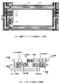
上記作製工程を用いた半導体素子からなる半導体回路を備えた半導体装置について、図1を用いてその構成を説明する。本実施例では図示を容易にするため、同一基板上に周辺駆動回路部の一部を構成するCMOS回路部と、画素マトリクス回路部の一部を構成する画素TFT(Nチャネル型TFT)とが示されている。
【0062】
また、図2(A)及び図2(B)は図1の上面図に相当する図であり、図2(A)及び図2(B)において、点線A−A’で切断した部分が、図1の画素マトリクス回路部の断面構造に相当し、点線B−B’で切断した部分が、図1のCMOS回路部の断面構造に相当する。また、図1及び図2に使われている符号は図3または図4と同一である。なお、図の簡略化のため、図2には、第1のマスク及び第2のマスクは図示していない。
【0063】
図1において、いずれのTFT(薄膜トランジスタ)も基板100上に設けられた下地膜101に形成される。CMOS回路のPチャネル型TFTの場合には、下地膜上にゲート配線102が形成され、その上にゲート絶縁膜103が設けられている。ゲート絶縁膜上には、活性層としてP型領域117(ソース領域又はドレイン領域)とチャネル形成領域112とが形成される。なお、活性層は同一パターン形状を有する第1の保護膜108と、第2の保護膜109で保護される。第2の保護膜109の上を覆う有機樹脂からなる第1の層間絶縁膜118にコンタクトホールが形成され、P型領域117に配線119、120が接続され、さらにその上に第2の層間絶縁膜125が形成され、配線119に引き出し配線126が接続されて、その上を覆って第3の層間絶縁膜129が形成される。なお、チャネル形成領域の上方の第2の保護膜上に、遮光性を有する第1のマスク110dが形成され、チャネル形成領域を劣化から保護している。この第1のマスク110dには、3価(本実施例ではボロン)及び5価(本実施例ではリン)の不純物が添加され、不純物の濃度が1×10¹⁹atoms /cm3 以上含まれている。
【0064】
一方、Nチャネル型のTFTは、活性層としてn+ 型領域114(ソース領域又はドレイン領域)と、チャネル形成領域112と、前記n+ 型領域(ドレイン領域)とチャネル形成領域の間にn- 型領域(LDD領域)115が形成される。n+ 型領域114のうち、ドレイン領域には配線120、ソース領域には121が形成され、さらに配線121には引き出し配線127が接続される。活性層以外の部分は、上記Pチャネル型TFTと概略同一構造である。なお、少なくともチャネル形成領域112の上方の第2の保護膜上に第1のマスク(110b及び110c)が形成され、n- 型領域114のうち一方の側のドレイン領域の上方の第2の保護膜上に、遮光性を有する第2のマスク113bが形成され、チャネル形成領域及びn- 型領域を光の劣化から保護している。
【0065】
画素マトリクス回路に形成されたNチャネル型TFTについては、ゲート絶縁膜103を形成する部分まで、CMOS回路のNチャネル型TFTと同一構造である。画素マトリクス回路に形成されたNチャネル型TFTにおいては、配線122及び123と接続されたn+ 型領域114とチャネル形成領域112との間に生じるホットキャリア注入などの劣化現象が発生しやすいため、配線と接続されたn+ 型領域とチャネル形成領域の間にn- 型領域(LDD領域)115を形成し、隣合うチャネル形成領域の間にはn- 型領域(LDD領域)を設けない構成とした。なおn- 型領域(LDD領域)115の形成の際に使用した第1のマスク及び第2のマスクを残有させ、そのまま遮光膜として用いた。そして、配線122、123が形成された第1の層間絶縁膜118上に第2の層間絶縁膜125と、ブラックマスク128とが形成される。さらに、その上に第3の層間絶縁膜129が形成され、ITO、SnO2 等の透明導電膜からなる画素電極130が接続される。なお、ブラックマスクは画素TFTを覆い、且つ画素電極130と補助容量を形成している。
【0066】
本実施例では、裏面露光によってレジストマスクを形成したため、ゲート配線の上方にはマスクが設けられており、他の配線との配線間容量を低減している。
【0067】
本実施例では一例として透過型のLCDを作製したが特に限定されない。例えば、画素電極の材料として反射性を有する金属材料を用い、画素電極のパターニングの変更、または幾つかの工程の追加/削除を適宜行えば反射型のLCDを作製することが可能である。
【0068】
なお、本実施例では、画素マトリクス回路の画素TFTのゲート配線をダブルゲート構造としているが、オフ電流のバラツキを低減するために、トリプルゲート構造等のマルチゲート構造としても構わない。また、開口率を向上させるためにシングルゲート構造としてもよい。
【0069】
〔実施例2〕本実施例は、実施例1とは異なる方法により結晶性半導体膜を得る例である。本実施例では、実施例1における図3(B)の工程と図3(C)の工程の間に、結晶化を助長する触媒元素を半導体膜全面または選択的に保持させる工程を加える。基本的な構成は実施例1とほぼ同様であるので、相違点のみに着目して説明する。
【0070】
本実施例は、半導体膜104を形成する工程(図3(B))までは、実施例1と同一である。
【0071】
次いで、本実施例では半導体膜104の表面に珪素の結晶化を助長する触媒元素を導入する。珪素の結晶化を助長する触媒元素としては、Ni、Fe、Co、Pt、Cu、Au、Geから選ばれた一種または複数種類の元素が用いられる。本実施例では前記触媒元素の内、非晶質珪素膜中の拡散速度が早く、極めて良好な結晶性を得ることができるNiを用いた。
【0072】
また、上記触媒元素を導入する箇所としては、特に限定されないが、非晶質珪素膜の全面、またはマスクを適宜形成することにより選択的に導入する。また、触媒元素を非晶質珪素膜の裏面、または表裏両面に導入する工程としてもよい。
【0073】
また、非晶質珪素膜に触媒元素を導入する方法としては、触媒元素を非晶質珪素膜の表面に接触させ得る方法、または非晶質珪素膜の膜中に保持させ得る方法であれば特に限定されない。例えば、スパッタ法、CVD法、プラズマ処理法、吸着法、イオン注入法、または触媒元素を含有した溶液を塗布する方法をしようることができる。この内、溶液を用いる方法は簡便であり、触媒元素の濃度調整が容易であるという点で有用である。金属塩としては各種塩を用いるとができ、溶媒としては水のほか、アルコール類、アルデヒド類、エーテル類、その他の有機溶媒、或いは水と有機溶媒の混合溶媒を用いることができる。本実施例では、塗布方法を用い、10〜10000ppm、好ましくは100〜10000ppm(重量換算)の範囲のニッケルを含んだ溶液を塗布した。ただし、非晶質珪素膜の膜厚を考慮に入れて適宜添加量を調節する必要がある。このようにして得られた非晶質珪素膜における膜中のニッケル濃度は1×10¹⁹〜1×10²¹atoms /cm3 となる。
【0074】
以上のようにして触媒元素を非晶質珪素膜に導入した後、レーザー光の照射により結晶化を行ない結晶性珪素膜を得る。また、レーザー光の照射に代えて高温加熱する工程を加えてもよい。また、膜中の触媒元素を低減させるゲッタリング工程を行う工程を加えてもよい。
【0075】
以降の工程は、実施例1に従えば図1で得られる半導体装置が得られる。
【0076】
〔実施例3〕 本実施例は、実施例1とは異なる方法により結晶性半導体膜を得る例である。本実施例では、レーザービーム形状を長方形または正方形に成形し、一度の照射で数cm2 〜数百cm2 の領域に均一なレーザー結晶化処理により結晶性珪素膜を得る方法に関する。基本的な構成は実施例1とほぼ同様であるので、相違点のみに着目して説明する。
【0077】
本実施例では、図3(C)の工程においてエキシマレーザー光を面状に加工して照射する。レーザー光を面状に加工する場合は数十cm2 程度(好ましくは10cm2 以上)の面積を一括照射できる様にレーザー光を加工する必要がある。そして照射面全体を所望のレーザーエネルギー密度でアニールするためには、トータルエネルギーが5J以上、好ましくは10J以上の出力のレーザー装置を用いる。
【0078】
その場合、エネルギー密度は100〜800mJ/cm2とし、出力パルス幅は100nsec以上、好ましくは200nsec〜1msecとすることが好ましい。200nsec〜1msecというパルス幅を実現するにはレーザー装置を複数台連結し、各レーザー装置の同期をずらすことで複数パルスの混合した状態を作れば良い。
【0079】
本実施例の様な面状のビーム形状を有するレーザー光を照射することにより大面積に均一なレーザー照射を行うことが可能である。即ち、活性層の結晶性(結晶粒径や欠陥密度等を含む)が均質なものとなり、TFT間の電気特性のばらつきを低減することができる。
【0080】
なお、本実施例は実施例1または2との組み合わせが容易であり、その組み合わせ方は自由である。
【0081】
〔実施例4〕 本実施例は、実施例1とは異なる方法により絶縁膜及び結晶性半導体膜を得る例である。
【0082】
本実施例では、ゲート絶縁膜として膜厚125nmの窒化酸化珪素膜、初期半導体膜として膜厚50nmの非晶質珪素膜、絶縁膜として15nmの窒化酸化珪素膜を大気にふれることなく積層形成した。勿論、それぞれの膜厚は本実施例に限定されることはなく、実施者が適宜決定すればよい。また、同一チャンバーで反応ガスを入れ換えることにより積層形成する構成としてもよい。また、前記初期半導体膜を成膜する前には被膜形成面上を、活性水素または水素化合物によって汚染物を減少させる構成とすることが好ましい。
【0083】
その後、初期半導体膜に対して赤外光または紫外光の照射による結晶化(以下、レーザー結晶化と呼ぶ)を行う。本実施例ではエキシマレーザー光を線状にビーム形成して照射した。なお、照射条件としては、パルス周波数が150Hz、オーバーラップ率は80〜98%、本実施例では96%、レーザーエネルギー密度は100〜500mJ/cm2、好ましくは150〜200mJ/cm2であり本実施例では175mJ/cm2とした。なお、レーザー結晶化の条件(レーザー光の波長、オーバーラップ率、照射強度、パルス幅、繰り返し周波数、照射時間等)は、絶縁膜の膜厚、初期半導体膜の膜厚、基板温度等を考慮して実施者が適宜決定すればよい。
【0084】
この工程により初期半導体膜は結晶化され、結晶性半導体膜(結晶を含む半導体膜)に変化する。本実施例において結晶性半導体膜とは多結晶珪素膜である。この工程において、レーザー光の照射は絶縁膜の上から行われるので初期半導体膜中に大気からの汚染物質が混入するおそれがない。即ち、初期半導体膜の界面の洗浄性を保ったまま、初期半導体膜の結晶化を行うことができる。
【0085】
こうして、図3(C)で得られる状態とほぼ同一の状態が得られる。以降の工程(図3(D)以降)は実施例1に従えば図1で得られる半導体装置が完成する。なお、本実施例は実施例1または3との組み合わせが容易であり、その組み合わせ方は自由である。
【0086】
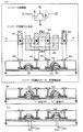
〔実施例5〕 本実施例では実施例1と異なる構造のTFTを作製した場合の例について図5を用いて説明する。また、図5の上面図は図2に相当する。
【0087】
本実施例では基板500としてプラスチック基板、下地膜501として酸化窒化シリコン(SiOxNyで示される)、ゲート配線として、銅(Cu)が主成分とする材料からなる膜を上層、タンタルを主成分とする材料からなる膜を下層とした積層構造とした。
【0088】
次に、第1絶縁膜503として、ゲート電極を有する領域と有さない領域との凹凸を平坦にする有機材料、例えばBCB(ベンゾシクロブテン)膜を100nm〜1μm (好ましくは500〜800nm)の厚さで形成する。この工程ではゲート配線による段差を完全に平坦化する程度の膜厚が必要である。BCB膜の平坦化効果は大きいので、さほど膜厚を厚くしなくても十分な平坦化が可能である。
【0089】
第1絶縁膜503を形成したら、次に第2絶縁膜(窒化酸化シリコン膜)504、初期半導体膜(微結晶シリコン膜)、保護膜509となる絶縁膜(窒化酸化シリコン膜)を順次大気開放しないで積層形成する。微結晶シリコン膜は、形成温度を80℃〜300℃、好ましくは、140〜200℃とし、水素で希釈したシランガス(SiH4 :H2 =1:10〜100)を反応ガスとし、ガス圧を0.1〜10Torr、放電電力を10〜300mW/cm2 とすることで形成される。微結晶シリコン膜は、膜中における水素濃度が低いため、初期半導体膜として用いれば、水素濃度を低減させる熱処理を省略することができる。本実施例では、第2の絶縁膜の形成専用のチャンバーと、初期半導体膜の形成専用のチャンバーと、保護膜の形成専用のチャンバーとを用意し、大気にふれることなく、各チャンバーを移動することにより連続的に成膜した。こうして連続成膜された絶縁膜及び半導体膜は平坦面上に形成されるため全て平坦である。
【0090】
次に、保護膜の上からエキシマレーザー光を照射することによって、半導体膜が結晶を含む半導体膜(多結晶シリコン膜)に変化する。このレーザー結晶化工程の条件は実施例4と同様で良い。この時、半導体膜が平坦であるので結晶粒径の均一な多結晶シリコン膜が得られる。また、レーザー光の照射に代えて強光の照射、例えばRTA、RTPを用いてもよい。
【0091】
以上の様に、第1絶縁膜503として平坦化に有利なBCB膜を用いることで平坦面を有する半導体膜を得ることができる。そのため、半導体膜の全域に渡って均一な結晶性を確保することができる。
【0092】
以降の工程は実施例1に従えば図5で得られる半導体装置が完成する。ただし、若干第2のマスク設計が異なる。
【0093】
図5においては、いずれのTFT(薄膜トランジスタ)も基板500上に設けられた下地膜501に形成される。CMOS回路のPチャネル型TFTの場合には、下地膜上にゲート配線502a、502bが形成され、その上にBCBからなる第1絶縁膜503、第2絶縁膜504が設けられている。第2絶縁膜上には、活性層としてP型領域508(ソース領域又はドレイン領域)とチャネル形成領域505とが形成される。なお、活性層は同形状を有する保護膜509で保護される。保護膜509の上を覆う第1の層間絶縁膜510にコンタクトホールが形成され、P型領域508に配線511、512が接続され、さらにその上に第2の層間絶縁膜516が形成され、配線511に引き出し配線517が接続されて、その上を覆って第3の層間絶縁膜520が形成される。なお、少なくともチャネル形成領域の上方の保護膜上に、遮光性を有する第1のマスクが形成され、チャネル形成領域を光の劣化から保護している。
【0094】
一方、Nチャネル型のTFTは、活性層としてn+ 型領域507(ソース領域又はドレイン領域)と、チャネル形成領域505と、前記n+ 型領域とチャネル形成領域の間にn- 型領域506が形成される。n+ 型領域507には配線512、513が形成され、さらに配線513には引き出し配線518が接続される。活性層以外の部分は、上記Pチャネル型TFTと概略同一構造である。なお、少なくともチャネル形成領域505の上方の保護膜上に、遮光性を有する第1のマスクが形成され、n- 型領域506の上方の保護膜上に、第2のマスクが形成され、チャネル形成領域およびn- 型領域を光の劣化から保護している。
【0095】
画素マトリクス回路に形成されたNチャネル型TFTについては、n+ 型領域507には配線514、515が接続され、その上に第2の層間絶縁膜516と、ブラックマスク519とが形成される。このブラックマスクは画素TFTを覆い、且つ配線515と補助容量を形成している。さらに、その上に第3の層間絶縁膜520が形成され、ITO等の透明導電膜からなる画素電極521が接続される。
【0096】
本実施例の画素マトリクス回路において、ゲート配線502と配線514、515の間で生じる配線間容量が、第1または第2のマスクによって低減されたTFT構造となっている。なお、画素マトリクス回路に限らず、本実施例では、裏面露光によってレジストマスクを形成したため、ゲート配線の上方にはマスクが設けられており、他の配線との配線間容量を低減している。
【0097】
本実施例を実施して作製されたTFTは、よりばらつきの少ない電気特性を示す。また、本実施例を実施例1〜4と組み合わせることは可能である。
【0098】
〔実施例6〕 本実施例では実施例1と異なる構造のTFTを作製した場合の例について図6を用いて説明する。なお、CMOS回路における構成は実施例1とほぼ同一であるので、相違点のみに着目して説明する。また、図6の上面図は図2に相当する。
【0099】
本実施例は、基板としてガラス基板、下地膜として酸化窒化珪素膜(SiOxNyで示される)、ゲート配線を形成する工程までは、実施例1と同一である。
【0100】
次いで、本実施例では、画素マトリクス回路において、選択的に第1絶縁膜601を形成する。
【0101】
その後、実施例1と同様に第2絶縁膜(実施例1ではゲート絶縁膜に相当する)、初期半導体膜を順次大気開放しないで積層形成する。本実施例では、同一チャンバー内で高真空を保ったまま、第2絶縁膜602として膜厚10〜100nmの窒化酸化珪素膜、初期半導体膜として膜厚50nmの非晶質珪素膜をプラズマCVD法を用いて積層形成した。勿論、それぞれの膜厚は本実施例に限定されることはなく、実施者が適宜決定すればよい。本実施例では、画素マトリクス回路において、ゲート絶縁膜(第1絶縁膜601及び第2絶縁膜602)の総膜厚が100〜300nmになるように形成した。
【0102】
以降の工程は実施例1に従えば図6で得られる半導体装置が完成する。
【0103】
図6においては、CMOS回路における構成は実施例1の図1とほぼ同一であるので省略する。画素マトリクス回路に形成されたNチャネル型TFTについては、ゲート絶縁膜が二層構造(第1絶縁膜601と第2絶縁膜602)となっている部分以外は、実施例1の図1とほぼ同一である。このように選択的にゲート絶縁膜の膜厚を厚くすることで、高耐圧が要求される回路(画素マトリクス回路、バッファ回路等)においての信頼性を向上させた。
【0104】
また、本実施例は実施例1と同様に画素マトリクス回路において、ゲート配線と他の配線との間で生じる配線間容量が、第1または第2のマスクによって低減されたTFT構造となっている。なお、画素マトリクス回路に限らず、本実施例では、裏面露光によってレジストマスクを形成したため、ゲート配線の上方にはマスクが設けられており、他の配線との配線間容量を低減している。
【0105】
本実施例を実施して作製されたTFTは、よりばらつきの少ない電気特性を示す。また、本実施例を実施例1乃至5のいずれか一と組み合わせることは可能である。
【0106】
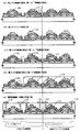
〔実施例7〕 本実施例では実施例1と異なる構造の画素マトリクス回路部を作製した場合の例について図7(A)〜(C)を用いて説明する。実施例1では、画素マトリクス回路部の画素TFTのゲート配線をダブルゲート構造としたが、本実施例では、オフ電流のバラツキを低減するために、トリプルゲート構造とした例を示す。
【0107】
図7(C)は、トリプルゲート構造の一例を示した上面図である。また、図7(C)中の点線A−A’で切断した断面の一例を図7(A)に示した。
【0108】
図7(A)において、701はn- 型領域(LDD領域)、702はゲート配線、703はn+ 型領域、704、705は配線、706はブラックマスク、707は画素電極、708、709は層間絶縁膜である。この構成における特徴は、LDD領域(チャネル長方向の幅が、0.5〜3μm、代表的には1〜2μm)が必要である箇所のみに設けられている点である。従来、特にセルフアライン法では、隣合うチャネル形成領域間に不必要なLDD領域が形成されていた。
【0109】
本実施例は、実施例1を応用することにより形成することができる。図7(A)に示される断面構造、特にn- 型領域(LDD領域)及びn+ 型領域を得るためには、実施例1における第2のマスクのパターン形状を変えることで容易に形成することができる。
【0110】
また、図7(A)とは異なる第2のマスクのパターンを用いることで、図7(B)で示すような異なる(LDD領域)の幅を工程を増やすことなく得ることができる。図7(B)は図7(B)とほとんど同一であるが、LDD領域のチャネル長方向の幅の広い第1のn- 型領域722、とLDD領域のチャネル長方向の幅の狭い第1のn- 型領域721を選択的に形成した。なお、第1のn- 型領域722のチャネル長方向の幅は、0.5〜3μm、代表的には1〜2μm、第2のn- 型領域721のチャネル長方向の幅は、0.3〜2μm、代表的には0.3〜0.7μmとする。n- 型領域のチャネル長方向の幅は、それぞれマスク設計によって自由に調節できる。従って、n- 型領域のチャネル長方向の幅は、回路構成の必要に応じて実施者が適宜決定すればよい。
【0111】
本実施例を実施して作製されたTFTは、よりばらつきの少ない電気特性を示す。また、本実施例を実施例1乃至6のいずれか一と組み合わせることは可能である。
【0112】
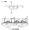
〔実施例8〕 本実施例では、実施例1に示したCMOS回路(インバータ回路)の回路構成の例について図8を用いて説明する。なお、図8(A)のインバータ回路図、インバータ回路の上面図における各端子部a、b、c、dは対応している。
【0113】
図8(A)に示すインバータ回路のA−A’断面構造図は図1に示したものと同一構造である。従って、図8(A)に示す構造を得るには、実施例1を適用すればよい。この回路構成はゲート配線801、Nチャネル型TFTのソース電極802、Nチャネル型TFTのソース電極803、共通ドレイン電極804から構成される。
【0114】
また、図8(A)のA−A’断面構造図とは異なるインバータ回路の断面構造図を図8(B)に示す。図8(B)に示す構造を得るためには、実施例1中の第2のマスク810のパターンを変更して、第2のマスク820をPチャネル型TFTにも形成し、ボロンが低濃度にドープされたP- 型領域822と、n- 型領域821を形成する。なお、図8(B)に示す構造を得るためには、ボロンを低濃度にするためのマスクが必要である。
【0115】
また、図8(A)のA−A’断面構造図とは異なるインバータ回路の断面構造図を図8(C)に示す。図8(C)に示す構造を得るためには、実施例1中の第2のマスク810のパターンを変更して、第2のマスク840を形成し、チャネル形成領域の両側にn- 型領域841を形成する。n- 型領域のチャネル長方向の幅は、それぞれマスク設計によって自由に調節できる。従って、n- 型領域のチャネル長方向の幅は、回路構成の必要に応じて実施者が適宜決定すればよい。また、ゲート配線831は、タンタル膜を形成後、表面に陽極酸化膜を形成した後、パターニングすることによって、マスク数を減らした。
【0116】
また、同一基板上に図8(A)の構造と図8(B)の構造を工程を増やすことなく同時に作製することは可能である。本発明を利用することによって、同一基板上に様々な(チャネル長方向の)幅を有するn- 型領域またはp- 型領域を形成することが可能である。例えば、同一基板上にチャネル形成領域の両側にn- 型領域を有するTFT、チャネル形成領域の片側にn- 型領域を有するTFT、チャネル形成領域の両側にチャネル長方向の幅の異なるn- 型領域を有するTFT、チャネル形成領域の両側にn- 型領域を有さないTFT等を工程を増やすことなく同時に作製することが可能である。
【0117】
また、本実施例を実施例1乃至6のいずれか一と組み合わせることは可能である。
【0118】
〔実施例9〕 本実施例では、実施例1〜6に示したボトムゲート型TFTを用いてバッファ回路を構成する場合の例について図9を用いて説明する。なお、CMOS回路は同一基板上に形成されたNチャネル型TFTとPチャネル型TFTとを相補的に組み合わせて構成する。なお、図9のバッファ回路図、バッファ回路の断面構造図における各端子部a、b、c、dは対応している。
【0119】
図示したようにバッファ回路においては、少なくともNチャネル型TFTのチャネル形成領域の片側(出力配線端子b側)にn- 型領域を形成することが好ましい。図9に示す構造を得るためには、実施例1中の第2のマスク110のパターンを変更して、第2のマスク910を形成し、チャネル形成領域の片側にn- 型領域901を形成する。
【0120】
また、本実施例を実施例1乃至6のいずれか一と組み合わせることは可能である。
【0121】
〔実施例10〕 本実施例では、本願発明によって作製された液晶表示装置の例を図10に示す。画素TFT(画素スイッチング素子)の作製方法やセル組工程は公知の手段を用いれば良いので詳細な説明は省略する。
【0122】
図10において1000は絶縁表面を有する基板(酸化シリコン膜を設けたプラスチック基板)、1001は画素マトリクス回路、1002は走査線駆動回路、1003は信号線駆動回路、1030は対向基板、1010はFPC(フレキシブルプリントサーキット)、1020はロジック回路である。ロジック回路1020としては、D/Aコンバータ、γ補正回路、信号分割回路などの従来ICで代用していた様な処理を行う回路を形成することができる。勿論、基板上にICチップを設けて、ICチップ上で信号処理を行うことも可能である。
【0123】
さらに、本実施例では液晶表示装置を例に挙げて説明しているが、アクティブマトリクス型の表示装置であればEL(エレクトロルミネッセンス)表示装置やEC(エレクトロクロミックス)表示装置に本願発明を適用することも可能であることは言うまでもない。
【0124】
また、本願発明を用いて作製できる液晶表示装置は透過型か反射型かは問わない。どちらを選択するのも実施者の自由である。この様に本願発明はあらゆるアクティブマトリクス型の電気光学装置(半導体装置)に対して適用することが可能である。
【0125】
なお、本実施例に示した半導体装置を作製するにあたって、実施例1〜実施例9のどの構成を採用しても良いし、各実施例を自由に組み合わせて用いることが可能である。
【0126】
〔実施例11〕 本願発明は従来のIC技術全般に適用することが可能である。即ち、現在市場に流通している全ての半導体回路に適用できる。例えば、ワンチップ上に集積化されたRISCプロセッサ、ASICプロセッサ等のマイクロプロセッサに適用しても良いし、液晶用ドライバー回路(D/Aコンバータ、γ補正回路、信号分割回路等)に代表される信号処理回路や携帯機器(携帯電話、PHS、モバイルコンピュータ)用の高周波回路に適用しても良い。
【0127】
また、マイクロプロセッサ等の半導体回路は様々な電子機器に搭載されて中枢回路として機能する。代表的な電子機器としてはパーソナルコンピュータ、携帯型情報端末機器、その他あらゆる家電製品が挙げられる。また、車両(自動車や電車等)の制御用コンピュータなども挙げられる。本願発明はその様な半導体装置に対しても適用可能である。
【0128】
なお、本実施例に示した半導体装置を作製するにあたって、実施例1〜実施例9のどの構成を採用しても良いし、各実施例を自由に組み合わせて用いることが可能である。
【0129】
〔実施例12〕 本願発明の電気光学装置は、様々な電子機器のディスプレイとして利用される。その様な電子機器としては、ビデオカメラ、デジタルカメラ、プロジェクター、プロジェクションTV、ゴーグルディスプレイ、カーナビゲーション、パーソナルコンピュータ、携帯情報端末(モバイルコンピュータ、携帯電話、電子書籍等)などが挙げられる。それらの一例を図11に示す。
【0130】
図11(A)は携帯電話であり、本体2001、音声出力部2002、音声入力部2003、表示装置2004、操作スイッチ2005、アンテナ2006で構成される。本願発明を音声出力部2002、音声入力部2003、表示装置2004やその他の信号制御回路に適用することができる。
【0131】
図11(B)はビデオカメラであり、本体2101、表示装置2102、音声入力部2103、操作スイッチ2104、バッテリー2105、受像部2106で構成される。本願発明を表示装置2102、音声入力部2103やその他の信号制御回路に適用することができる。
【0132】
図11(C)はモバイルコンピュータ(モービルコンピュータ)であり、本体2201、カメラ部2202、受像部2203、操作スイッチ2204、表示装置2205で構成される。本願発明は表示装置2205やその他の信号制御回路に適用できる。
【0133】
図11(D)はゴーグルディスプレイであり、本体2301、表示装置2302、アーム部2303で構成される。本発明は表示装置2302やその他の信号制御回路に適用することができる。
【0134】
図11(E)はリア型プロジェクターであり、本体2401、光源2402、表示装置2403、偏光ビームスプリッタ2404、リフレクター2405、2406、スクリーン2407で構成される。本発明は表示装置2403やその他の信号制御回路に適用することができる。
【0135】
図11(F)は携帯書籍(電子書籍)であり、本体2501、表示装置2502、2503、記憶媒体2504、操作スイッチ2505、アンテナ2506で構成される。本発明は表示装置2502、2503やその他の信号制御回路に適用することができる。
【0136】
以上の様に、本願発明の適用範囲は極めて広く、あらゆる分野の電子機器に適用することが可能である。
【0137】
なお、本実施例に示した半導体装置を作製するにあたって、実施例1〜実施例6のどの構成を採用しても良いし、各実施例を自由に組み合わせて用いることが可能である。また、実施例7〜10、実施例11に示した電気光学装置や半導体回路をその様に組み合わせて用いても良い。
【0138】
【発明の効果】
本願発明を実施することで、再現性が高くTFTの安定性を向上し、生産性の高いLDD構造を備えたTFTを得ることができる。
【0139】
本発明を利用することにより、実施者は、回路構成の必要に応じて適宜第2のマスクのマスク設計を決定することにより、TFTのチャネル形成領域の両側または片側に、所望のLDD領域を形成することができる。例えば、チャネル長方向の幅が、0.5〜3μm、代表的には1〜2μmである第1のLDD領域を有する第1のNチャネル型TFTと、チャネル長方向の幅が、0.3〜2μm、代表的には0.3〜0.7μmである第2のLDD領域を有する第2のNチャネル型TFTと、
【0140】
また、LDD構造を形成するために使用されたマスクをそのまま遮光膜として用い、活性層、特にチャネル形成領域を光の劣化から保護して信頼性を向上することが実現できる。また、マスクの除去工程を省略することで、短時間でのTFTの製造を可能とした。
【0141】
さらに、本発明を用いてLDD領域を形成するためには、(ソース/ドレイン電極形成まで)マスク数が従来(最低8枚)よりも少ないマスク数(最低7枚)とすることができた。
マスク▲1▼ゲート配線の形成
マスク▲2▼アイランドの形成
マスク▲3▼第2のマスクの形成
マスク▲4▼P型の導電性を付与するドーピングマスクの形成
マスク▲5▼ソース/ドレイン領域へのコンタクトホールの形成
マスク▲6▼ゲート配線へのコンタクトホールの形成
マスク▲7▼ソース/ドレイン電極の形成
【0142】
また、本発明を実施するにあたっては、幾つかの装置を導入するだけで従来のアモルファスシリコンTFTの製造ラインをそのまま使用することが可能であるため、工業上、有益である。
【0143】
加えて、ゲート配線と他の配線との交差部においては、マスクが絶縁膜として機能するため、配線間容量を低減してTFTの電気特性を向上することが実現できる。
【0144】
また、大気にふれることなくゲート絶縁膜と半導体膜を積層形成することで、極めて清浄な界面を実現することができる。この様な構成により、特にTFTの電気特性を左右する活性層とゲート絶縁膜との界面を清浄なものとすることができるので、ばらつきが少なく、且つ、良好な電気特性を示すTFTが実現される。
【0145】
この時、TFTの代表的なパラメータであるしきい値電圧はNチャネル型TFTで−0.5〜2V、Pチャネル型TFTで0.5〜−2Vを実現できる。また、サブスレッショルド係数(S値)は0.1〜0.3V/decadeを実現できる。
【図面の簡単な説明】
【図1】 半導体装置の構造の一例を示す断面図(実施例1)。
【図2】 画素マトリクス回路及びCMOS回路の上面図(実施例1)。
【図3】 TFTの作製工程を示す図(実施例1)。
【図4】 TFTの作製工程を示す図(実施例1)。
【図5】 半導体装置の構造の一例を示す断面図(実施例5)。
【図6】 半導体装置の構造の一例を示す断面図(実施例6)。
【図7】 画素マトリクス回路部の一例を示す断面図及び上面図(実施例7)。
【図8】 インバータ回路図、上面図及び断面構造図の一例を示す断面図(実施例8)。
【図9】 バッファ回路図及び断面構造図(実施例9)。
【図10】 半導体装置(液晶表示装置)の構成を示す図(実施例10)。
【図11】 半導体装置(電子機器)の例を示す図(実施例12)。
【図12】 成膜装置の一例を示す図(実施例1)。
【符号の説明】
100 基板
101 下地膜
102 ゲート配線
103 ゲート絶縁膜
104 半導体膜(初期半導体膜)
105 絶縁膜
106 酸化膜
107 結晶性半導体膜
108 第1の保護膜
109 第2の保護膜
110a〜d 第1のマスク
111、115 n- 領域(低濃度不純物領域)
112 チャネル形成領域
113a、113b 第2のマスク
114 n+ 領域(高濃度不純物領域)
116 第3のマスク
117 P型領域(高濃度不純物領域)
118 第1の層間絶縁膜
119〜123 配線[0001]
[Technical field to which the invention belongs]
The present invention relates to a structure of a semiconductor device including a semiconductor circuit made of a semiconductor element such as an insulated gate transistor and a manufacturing method thereof. In particular, the present invention relates to a structure of a semiconductor device including a semiconductor circuit including a semiconductor element having an LDD structure formed using an organic resin and a manufacturing method thereof. The semiconductor device of the present invention includes not only an element such as a thin film transistor (TFT) and a MOS transistor but also an electro-optical device such as a display device and an image sensor having a semiconductor circuit composed of these insulated gate transistors. In addition, the semiconductor device of the present invention includes an electronic apparatus in which these display device and electro-optical device are mounted.
[0002]
[Prior art]
Conventionally, a TFT is used as a switching element of an active matrix liquid crystal display device (hereinafter abbreviated as AMLCD). At present, products having a circuit configuration with TFTs using an amorphous silicon film (amorphous silicon film) as an active layer occupy the market. In particular, as the TFT structure, an inverted stagger structure with a simple manufacturing process is often employed.
[0003]
However, as the performance of AMLCDs increases year by year, the operating performance (especially the operating speed) required for TFTs tends to be severe. Therefore, it has become difficult to obtain an element having sufficient performance at the operating speed of a TFT using an amorphous silicon film.
[0004]
Accordingly, TFTs using a polycrystalline silicon film (polysilicon film) instead of an amorphous silicon film have attracted attention, and development of TFTs using a polycrystalline silicon film as an active layer has been proceeding at a remarkable pace. At present, some of them are commercialized.
[0005]
Many presentations have already been made on the structure of an inverted staggered TFT using a polycrystalline silicon film as an active layer. However, the conventional inverted stagger structure has various problems.
[0006]
First, since the entire active layer is as thin as about 50 nm, impact ionization occurs at the junction between the channel formation region and the drain region, and a deterioration phenomenon such as hot carrier injection appears remarkably. Therefore, it becomes necessary to form an LDD region (Light Doped Drain region).
[0007]
In order to form this LDD region, it is expected that at least eight masks (up to source / drain electrode formation) are necessary in the structure of the conventional inverted stagger type TFT.
[0008]
As described above, in the structure of the conventional inverted stagger type TFT, the LDD region must be formed in a lateral plane on both sides or one side of the channel formation region, and the reproducible LDD region is formed. It is very difficult.
[0009]
[Problems to be solved by the present invention]
It is an object of the present invention to provide a technique for manufacturing a semiconductor device with high productivity and high reliability and reproducibility by a very simple manufacturing process.
[0010]
[Means for Solving the Problems]
The first configuration of the invention disclosed in this specification is:
Gate wiring on an insulating surface;
A gate insulating film in contact with the gate wiring;
A channel formation region provided on the gate wiring via the gate insulating film;
A low-concentration impurity region in contact with the channel formation region;
A high concentration impurity region in contact with the low concentration impurity region;
A protective film in contact with the channel formation region;
A semiconductor device including a semiconductor circuit including a semiconductor element, which has an organic resin to which a trivalent or pentavalent impurity is added in contact with the protective film.
[0011]
In addition, the second configuration of the invention disclosed in this specification is as follows.
Gate wiring on an insulating surface;
A gate insulating film in contact with the gate wiring;
A channel formation region provided on the gate wiring via the gate insulating film;
A low-concentration impurity region provided on one side of the channel formation region;
A drain region composed of a first high concentration impurity region in contact with the low concentration impurity region;
A source region comprising a second high-concentration impurity region provided on the other side of the channel formation region;
A protective film in contact with the channel formation region;
A semiconductor device including a semiconductor circuit including a semiconductor element, which has an organic resin to which a trivalent or pentavalent impurity is added in contact with the protective film.
[0012]
Further, the third configuration of the invention disclosed in this specification is as follows.
Gate wiring on an insulating surface;
A gate insulating film in contact with the gate wiring;
A channel formation region provided on the gate wiring via the gate insulating film;
A first low-concentration impurity region and a second low-concentration impurity region in contact with the channel formation region;
A high concentration impurity region in contact with the first low concentration impurity region and the second low concentration impurity region;
A protective film in contact with the channel formation region;
An organic resin to which a trivalent or pentavalent impurity is added in contact with the protective film;
The width of the first low-concentration impurity region in the channel length direction is different from the width of the second low-concentration impurity region in the channel length direction.
[0013]
In each of the above structures, the gate wiring has a single layer structure or a stacked structure, and a kind of element selected from tantalum, copper, chromium, aluminum, molybdenum, titanium, and silicon, or a P-type or N-type impurity is added. It is characterized by being made of a material mainly composed of silicon.
[0014]
In each of the above structures, the trivalent or pentavalent impurity is phosphorus or boron.
[0015]
In each of the above structures, the organic resin has photosensitivity.
[0016]
In each of the above structures, the concentration of trivalent or pentavalent impurities in the organic resin is 1 × 10 19 atoms / cm Three It is characterized by the above.
[0017]
In each of the above structures, the high-concentration impurity region contains a catalytic element that promotes crystallization of silicon.
[0018]
The catalytic element is at least one element selected from Ni, Fe, Co, Pt, Cu, and Au, or a plurality of elements. Further, the catalyst element is Ge or Pb.
[0019]
Note that in this specification, the “initial semiconductor film” is a generic term for a semiconductor film, and is typically a semiconductor film having an amorphous structure such as an amorphous semiconductor film (such as an amorphous silicon film), a fine film. It refers to an amorphous semiconductor film having a crystal, a microcrystalline semiconductor film, and these semiconductor films include a Si film, a Ge film, a compound semiconductor film [for example, Si X Ge 1-X (0 <X <1), typically an amorphous silicon germanium film represented by X = 0.3 to 0.95, etc.]). This initial semiconductor film can be formed using a known technique, for example, a low pressure CVD method, a thermal CVD method, a PCVD method, a sputtering method or the like.
[0020]
Note that in this specification, a “crystalline semiconductor film” refers to a single crystal semiconductor film, a semiconductor film including a crystal grain boundary (including a polycrystalline semiconductor film and a microcrystalline semiconductor film), and is amorphous over the entire region. The distinction from the state semiconductor (amorphous semiconductor film) is made clear. Needless to say, the term “semiconductor film” in this specification includes an amorphous semiconductor film in addition to a crystalline semiconductor film.
[0021]
In this specification, the “semiconductor element” refers to a switching element or a memory element, such as a thin film transistor (TFT) or a thin film diode (TFD).
[0022]
In addition, the configuration of the first manufacturing method for manufacturing a semiconductor device including a semiconductor circuit including the semiconductor element of the present invention is as follows.
A first step of sequentially forming a gate insulating film and an initial semiconductor film on the insulating surface on which the gate wiring is formed without being exposed to the atmosphere;
A second step of crystallizing the initial semiconductor film by irradiating infrared light or ultraviolet light to form a crystalline semiconductor film and simultaneously forming an oxide film;
A region to be a channel formation region of the crystalline semiconductor film is covered with a mask, and the trivalent or pentavalent impurity element is added to a region to be a source region or a drain region of the crystalline semiconductor film through the oxide film. A third step of performing
A method for manufacturing a semiconductor device including a semiconductor circuit including a semiconductor element.
[0023]
In the first manufacturing method, after the first step, the initial semiconductor film has a step of holding a catalytic element for promoting crystallization of silicon in contact with the surface, or holding it in the film. Yes.
[0024]
In addition, the configuration of the second manufacturing method for manufacturing a semiconductor device including a semiconductor circuit including the semiconductor element of the present invention is as follows.
A step of sequentially stacking a gate insulating film, an initial semiconductor film, and an insulating film on the insulating surface where the gate wiring is formed without touching the atmosphere;
Irradiating infrared light or ultraviolet light through the insulating film to crystallize the initial semiconductor film to obtain a crystalline semiconductor film;
A region to be a channel formation region of the crystalline semiconductor film is covered with a mask, and a trivalent or pentavalent impurity element is added to the region to be a source region or a drain region of the crystalline semiconductor film through the insulating film. A process of performing;
A method for manufacturing a semiconductor device including a semiconductor circuit including a semiconductor element including
[0025]
In the second manufacturing method, the gate insulating film, the initial semiconductor film, and the protective film are formed using different chambers.
[0026]
In the second manufacturing method, the gate insulating film, the initial semiconductor film, and the protective film are formed using the same chamber.
[0027]
In the second manufacturing method, the gate insulating film and the protective film are formed using a first chamber,
The initial semiconductor film is formed using a second chamber.
[0028]
In the structure of each of the above manufacturing methods, contaminants are reduced on the film forming surface by active hydrogen or a hydrogen compound before forming the initial semiconductor film.
[0029]
Each of the above manufacturing methods has a step of forming a stacked film including a silicon nitride film in any layer as the gate insulating film.
[0030]
The structure of each manufacturing method is characterized in that it includes a step of forming a stacked film containing BCB (benzocyclobutene) as part of the gate insulating film.
[0031]
DETAILED DESCRIPTION OF THE INVENTION
The embodiment of the present invention having the above-described configuration will be described in detail with the examples described below.
[0032]
【Example】
Example 1 A typical example using the present invention will be described with reference to FIGS. In this embodiment, description will be made using a CMOS circuit constituting a part of the peripheral drive circuit part and a pixel TFT constituting a part of the pixel matrix circuit part on the same substrate. First, a method for manufacturing a semiconductor device including a semiconductor circuit including the semiconductor element of the present invention will be described with reference to FIGS.
[0033]
First, the
[0034]
Next, a
[0035]
Next, the
[0036]
Next, the
[0037]
In this embodiment, a silicon nitride oxide film with a thickness of 125 nm is stacked as the
[0038]
As the
[0039]
As the
[0040]
3B is obtained, the
[0041]
In this embodiment, laser crystallization is used as the crystallization technique, but other known means such as a solid phase growth method or a solid phase growth method using a catalytic element can also be used. In this embodiment, an oxide film is formed simultaneously with laser crystallization. However, a thin insulating film (silicon oxide film, silicon nitride film, silicon oxynitride film, etc.) is formed before or after laser irradiation, or an inert atmosphere. The step may be a step in which laser crystallization is performed and no oxide film is formed.
[0042]
Note that, after the step of FIG. 3C, an impurity may be added to control the threshold value, and a step of selectively adding the impurity to a region to be a channel formation region may be added.
[0043]
Next, the gate insulating film, the crystalline semiconductor film, and the oxide film were patterned to form an
[0044]
Next, a second
[0045]
Next, a first mask (resist mask in this embodiment) 110a having a film thickness of 1 to 3 μm was formed by exposure from the back surface in contact with the second
[0046]
In addition, the inorganic insulating film is patterned in order to form the first mask, the first mask is made into a laminated structure without removing the patterning mask made of organic resin at that time, the lower layer is an inorganic insulating film, and the upper layer is organic It is good also as a structure made into resin.
[0047]
Note that the formation of the resist by exposure from the back surface does not require a mask, so the number of manufacturing masks can be reduced. In this embodiment, an example is shown in which the width of the first mask in the channel length direction is slightly smaller than the width of the gate wiring due to the wraparound of light. However, the width may be substantially the same. It is possible to change the width of the mask in the channel length direction.
[0048]
Note that in this specification, when the
[0049]
Then, by using the
[0050]
Next, a second mask (a polyimide resin having photosensitivity in this embodiment) 113a having a thickness of 1 to 3 μm was formed in contact with the second
[0051]
Then, by using the
[0052]
An LDD structure is formed by the first and second impurity addition steps. Depending on the pattern shape of the second mask, n - Type region and n + The boundary of the mold area is determined. Note that in an N-channel TFT, n + The
[0053]
In the first and second impurity addition steps, the
[0054]
Next, the N-channel TFT is covered with a
[0055]
In this specification, intrinsic refers to a region that does not contain any impurities that can change the Fermi level of silicon, and the substantially intrinsic region is a balance between electrons and holes that offset the conductivity type. Region, that is, a concentration range in which threshold control is possible (1 × 10 3 by SIMS analysis) 15 ~ 1x10 17 atoms / cm Three ) Shows a region containing an impurity imparting N-type or P-type, or a region in which the conductivity type is offset by intentionally adding a reverse conductivity type impurity.
[0056]
The first to third impurities may be added using a known means such as an ion implantation method, a plasma doping method, or a laser doping method. However, the doping condition, dose, acceleration voltage, and the like are adjusted so that a desired amount of impurity ions is added to a predetermined region of the active layer through the first
[0057]
Further, in the first to third impurity addition steps, since impurities are injected from above the second
[0058]
Thus, after the high
[0059]
Next, a known technique such as thermal annealing or laser annealing is performed to obtain an impurity activation effect in the source region and the drain region, or a recovery effect of the crystal structure of the active layer damaged in the doping process.
[0060]
Finally, organic resin such as polyimide, polyimide amide, polyamide, acrylic, silicon oxide film, silicon nitride film, silicon nitride oxide film (SiO X N y Or an interlayer insulating
[0061]
A structure of a semiconductor device including a semiconductor circuit including a semiconductor element using the above manufacturing process will be described with reference to FIGS. In this embodiment, for ease of illustration, a CMOS circuit portion that constitutes a part of the peripheral drive circuit portion and a pixel TFT (N-channel TFT) that constitutes a part of the pixel matrix circuit portion on the same substrate. It is shown.
[0062]
2 (A) and 2 (B) are views corresponding to the top view of FIG. 1, and in FIG. 2 (A) and FIG. 2 (B), the portion cut along the dotted line AA ′ is 1 corresponds to the cross-sectional structure of the pixel matrix circuit portion in FIG. 1, and the portion cut along the dotted line BB ′ corresponds to the cross-sectional structure of the CMOS circuit portion in FIG. The reference numerals used in FIGS. 1 and 2 are the same as those in FIG. 3 or FIG. For simplification of the drawing, the first mask and the second mask are not shown in FIG.
[0063]
In FIG. 1, any TFT (thin film transistor) is formed on a
[0064]
On the other hand, an N-channel TFT has n as an active layer. + Mold region 114 (source region or drain region),
[0065]
The N-channel TFT formed in the pixel matrix circuit has the same structure as the N-channel TFT of the CMOS circuit up to the portion where the
[0066]
In this embodiment, since the resist mask is formed by backside exposure, a mask is provided above the gate wiring to reduce the capacitance between wirings with other wirings.
[0067]
In this embodiment, a transmissive LCD is manufactured as an example, but is not particularly limited. For example, a reflective LCD can be manufactured by using a reflective metal material as a material for the pixel electrode and appropriately changing the patterning of the pixel electrode or adding / deleting some processes as appropriate.
[0068]
In this embodiment, the gate wiring of the pixel TFT of the pixel matrix circuit has a double gate structure. However, a multi-gate structure such as a triple gate structure may be used in order to reduce variation in off current. Further, a single gate structure may be used in order to improve the aperture ratio.
[0069]
[Embodiment 2] This embodiment is an example in which a crystalline semiconductor film is obtained by a method different from that of Embodiment 1. In this embodiment, a step of selectively holding the catalyst element for promoting crystallization on the entire surface of the semiconductor film is added between the step of FIG. 3B and the step of FIG. Since the basic configuration is substantially the same as that of the first embodiment, only the differences will be described.
[0070]
This embodiment is the same as Embodiment 1 up to the step of forming the semiconductor film 104 (FIG. 3B).
[0071]
Next, in this embodiment, a catalytic element that promotes crystallization of silicon is introduced into the surface of the
[0072]
Further, the location where the catalyst element is introduced is not particularly limited, but the catalyst element is selectively introduced by appropriately forming the entire surface of the amorphous silicon film or a mask. Alternatively, the catalyst element may be introduced into the back surface or both front and back surfaces of the amorphous silicon film.
[0073]
Further, as a method for introducing the catalytic element into the amorphous silicon film, any method can be used as long as the catalytic element can be brought into contact with the surface of the amorphous silicon film, or can be retained in the amorphous silicon film. There is no particular limitation. For example, a sputtering method, a CVD method, a plasma processing method, an adsorption method, an ion implantation method, or a method of applying a solution containing a catalytic element can be used. Among these, the method using a solution is simple and useful in that the concentration of the catalyst element can be easily adjusted. Various salts can be used as the metal salt. As the solvent, water, alcohols, aldehydes, ethers, other organic solvents, or a mixed solvent of water and an organic solvent can be used. In this example, a solution containing nickel in a range of 10 to 10000 ppm, preferably 100 to 10000 ppm (weight conversion) was applied using a coating method. However, it is necessary to adjust the addition amount appropriately in consideration of the thickness of the amorphous silicon film. The nickel concentration in the amorphous silicon film thus obtained is 1 × 10 19 ~ 1x10 twenty one atoms / cm Three It becomes.
[0074]
After introducing the catalyst element into the amorphous silicon film as described above, crystallization is performed by laser light irradiation to obtain a crystalline silicon film. Moreover, it may replace with laser beam irradiation and may add the process heated at high temperature. In addition, a step of performing a gettering step for reducing the catalytic element in the film may be added.
[0075]
If the subsequent steps are in accordance with Example 1, the semiconductor device obtained in FIG. 1 is obtained.
[0076]
[Embodiment 3] This embodiment is an example in which a crystalline semiconductor film is obtained by a method different from that in Embodiment 1. In this embodiment, the laser beam shape is formed into a rectangle or square and is several cm with a single irradiation. 2 ~ Several hundred cm 2 The present invention relates to a method of obtaining a crystalline silicon film by uniform laser crystallization treatment in the region. Since the basic configuration is substantially the same as that of the first embodiment, only the differences will be described.
[0077]
In this embodiment, excimer laser light is processed into a planar shape and irradiated in the step of FIG. Dozens of centimeters when processing laser light into a surface 2 Degree (preferably 10 cm 2 It is necessary to process the laser beam so that the above area) can be collectively irradiated. In order to anneal the entire irradiated surface with a desired laser energy density, a laser device having an output with a total energy of 5 J or more, preferably 10 J or more is used.
[0078]
In that case, the energy density is 100 to 800 mJ / cm. 2 The output pulse width is 100 nsec or more, preferably 200 nsec to 1 msec. In order to realize a pulse width of 200 nsec to 1 msec, a plurality of laser devices are connected, and a state in which a plurality of pulses are mixed is created by shifting the synchronization of the laser devices.
[0079]
By irradiating a laser beam having a planar beam shape as in this embodiment, it is possible to perform uniform laser irradiation over a large area. That is, the crystallinity (including crystal grain size and defect density) of the active layer becomes uniform, and variations in electrical characteristics between TFTs can be reduced.
[0080]
Note that this embodiment can be easily combined with Embodiment 1 or 2, and the combination is free.
[0081]
[Embodiment 4] This embodiment is an example in which an insulating film and a crystalline semiconductor film are obtained by a method different from that in Embodiment 1.
[0082]
In this embodiment, a silicon nitride oxide film with a thickness of 125 nm is formed as a gate insulating film, an amorphous silicon film with a thickness of 50 nm is formed as an initial semiconductor film, and a silicon nitride oxide film with a thickness of 15 nm is formed as an insulating film without being exposed to the atmosphere. . Of course, each film thickness is not limited to the present embodiment, and the practitioner may determine it appropriately. Alternatively, a stack may be formed by exchanging the reaction gas in the same chamber. Further, it is preferable that the surface on which the film is formed is made to reduce contaminants with active hydrogen or a hydrogen compound before forming the initial semiconductor film.
[0083]
Thereafter, the initial semiconductor film is crystallized by irradiation with infrared light or ultraviolet light (hereinafter referred to as laser crystallization). In this embodiment, excimer laser light was formed into a linear beam and irradiated. As irradiation conditions, the pulse frequency is 150 Hz, the overlap rate is 80 to 98%, 96% in this embodiment, and the laser energy density is 100 to 500 mJ / cm. 2 , Preferably 150-200mJ / cm 2 In this embodiment, 175 mJ / cm 2 It was. Laser crystallization conditions (laser light wavelength, overlap rate, irradiation intensity, pulse width, repetition frequency, irradiation time, etc.) take into consideration the film thickness of the insulating film, the initial semiconductor film, the substrate temperature, The practitioner may determine as appropriate.
[0084]
By this step, the initial semiconductor film is crystallized and changed to a crystalline semiconductor film (a semiconductor film including a crystal). In this embodiment, the crystalline semiconductor film is a polycrystalline silicon film. In this step, since the laser beam is irradiated from above the insulating film, there is no possibility that contaminants from the atmosphere are mixed in the initial semiconductor film. That is, the initial semiconductor film can be crystallized while maintaining the cleanability of the interface of the initial semiconductor film.
[0085]
In this way, almost the same state as that obtained in FIG. If the subsequent steps (FIG. 3D and subsequent steps) are performed according to the first embodiment, the semiconductor device obtained in FIG. 1 is completed. Note that this embodiment can be easily combined with the first or third embodiment, and the combination is free.
[0086]
[Embodiment 5] In this embodiment, an example in which a TFT having a structure different from that of Embodiment 1 is manufactured will be described with reference to FIGS. The top view of FIG. 5 corresponds to FIG.
[0087]
In this embodiment, a plastic substrate is used as the
[0088]
Next, as the first insulating
[0089]
After the first insulating
[0090]
Next, by irradiating excimer laser light from above the protective film, the semiconductor film changes to a semiconductor film containing crystals (polycrystalline silicon film). The conditions for this laser crystallization step may be the same as in Example 4. At this time, since the semiconductor film is flat, a polycrystalline silicon film having a uniform crystal grain size can be obtained. Further, instead of laser light irradiation, strong light irradiation, for example, RTA or RTP may be used.
[0091]
As described above, a semiconductor film having a flat surface can be obtained by using a BCB film advantageous for planarization as the first insulating
[0092]
If the subsequent steps are in accordance with Example 1, the semiconductor device obtained in FIG. 5 is completed. However, the second mask design is slightly different.
[0093]
In FIG. 5, any TFT (thin film transistor) is formed on the
[0094]
On the other hand, an N-channel TFT has n as an active layer. + A mold region 507 (source region or drain region), a
[0095]
For N-channel TFTs formed in the pixel matrix circuit, n + Wirings 514 and 515 are connected to the
[0096]
The pixel matrix circuit of this embodiment has a TFT structure in which the interwiring capacitance generated between the gate wiring 502 and the
[0097]
A TFT manufactured by implementing this embodiment shows electric characteristics with less variation. In addition, this embodiment can be combined with Embodiments 1 to 4.
[0098]
[Embodiment 6] In this embodiment, an example in which a TFT having a structure different from that of Embodiment 1 is manufactured will be described with reference to FIGS. Since the configuration of the CMOS circuit is almost the same as that of the first embodiment, only the differences will be described. The top view of FIG. 6 corresponds to FIG.
[0099]
This example is the same as Example 1 up to the step of forming a glass substrate as a substrate, a silicon oxynitride film (indicated by SiOxNy) as a base film, and a gate wiring.
[0100]
Next, in this embodiment, the first insulating
[0101]
Thereafter, similarly to the first embodiment, a second insulating film (corresponding to a gate insulating film in the first embodiment) and an initial semiconductor film are sequentially stacked without being exposed to the atmosphere. In this embodiment, while maintaining a high vacuum in the same chamber, a plasma CVD method is applied to a silicon nitride oxide film having a thickness of 10 to 100 nm as the second
[0102]
If the subsequent steps are in accordance with the first embodiment, the semiconductor device obtained in FIG. 6 is completed.
[0103]
In FIG. 6, the configuration of the CMOS circuit is substantially the same as that of FIG. The N-channel TFT formed in the pixel matrix circuit is almost the same as FIG. 1 of the first embodiment except for the portion where the gate insulating film has a two-layer structure (first insulating
[0104]
Further, in this embodiment, as in the first embodiment, the pixel matrix circuit has a TFT structure in which the interwiring capacitance generated between the gate wiring and the other wiring is reduced by the first or second mask. . In addition to the pixel matrix circuit, in this embodiment, the resist mask is formed by backside exposure. Therefore, a mask is provided above the gate wiring, and the wiring capacitance with other wiring is reduced.
[0105]
A TFT manufactured by implementing this embodiment shows electric characteristics with less variation. In addition, this embodiment can be combined with any one of Embodiments 1 to 5.
[0106]
[Embodiment 7] In this embodiment, an example in which a pixel matrix circuit portion having a structure different from that of Embodiment 1 is manufactured will be described with reference to FIGS. In the first embodiment, the gate wiring of the pixel TFT in the pixel matrix circuit portion has a double gate structure. However, in this embodiment, an example of a triple gate structure is shown in order to reduce variation in off current.
[0107]
FIG. 7C is a top view illustrating an example of a triple gate structure. FIG. 7A shows an example of a cross section cut along a dotted line AA ′ in FIG.
[0108]
In FIG. 7A, 701 is n. - Mold region (LDD region), 702 is a gate wiring, 703 is n + The mold region, 704 and 705 are wirings, 706 is a black mask, 707 is a pixel electrode, and 708 and 709 are interlayer insulating films. A feature of this configuration is that it is provided only at a location where an LDD region (width in the channel length direction is 0.5 to 3 μm, typically 1 to 2 μm) is required. Conventionally, particularly in the self-alignment method, an unnecessary LDD region has been formed between adjacent channel formation regions.
[0109]
The present embodiment can be formed by applying the first embodiment. The cross-sectional structure shown in FIG. - Mold region (LDD region) and n + In order to obtain the mold region, it can be easily formed by changing the pattern shape of the second mask in the first embodiment.
[0110]
Further, by using a second mask pattern different from that in FIG. 7A, a different width (LDD region) as shown in FIG. 7B can be obtained without increasing the number of steps. FIG. 7B is almost the same as FIG. 7B, but the first n having a wide width in the channel length direction of the LDD region. -
[0111]
A TFT manufactured by implementing this embodiment shows electric characteristics with less variation. In addition, this embodiment can be combined with any one of Embodiments 1 to 6.
[0112]
[Embodiment 8] In this embodiment, an example of a circuit configuration of the CMOS circuit (inverter circuit) shown in Embodiment 1 will be described with reference to FIG. Note that the terminal portions a, b, c, and d in the inverter circuit diagram of FIG. 8A and the top view of the inverter circuit correspond to each other.
[0113]
The cross-sectional structure diagram of the inverter circuit shown in FIG. 8A is the same as that shown in FIG. Therefore, the first embodiment may be applied to obtain the structure shown in FIG. This circuit configuration includes a
[0114]
Further, FIG. 8B shows a cross-sectional structure diagram of an inverter circuit different from the AA ′ cross-sectional structure diagram of FIG. In order to obtain the structure shown in FIG. 8B, the pattern of the
[0115]
Further, FIG. 8C shows a cross-sectional structure diagram of an inverter circuit different from the AA ′ cross-sectional structure diagram of FIG. In order to obtain the structure shown in FIG. 8C, the pattern of the
[0116]
Further, the structure of FIG. 8A and the structure of FIG. 8B can be manufactured over the same substrate without increasing the number of steps. By utilizing the present invention, n having various widths (in the channel length direction) on the same substrate. - Type region or p - A mold region can be formed. For example, n on both sides of the channel formation region on the same substrate - TFT with mold region, n on one side of channel formation region - N having different widths in the channel length direction on both sides of the channel formation region - TFT having a mold region, n on both sides of the channel formation region - It is possible to simultaneously manufacture a TFT or the like that does not have a mold region without increasing the number of steps.
[0117]
In addition, this embodiment can be combined with any one of Embodiments 1 to 6.
[0118]
[Embodiment 9] In this embodiment, an example in which a buffer circuit is configured using the bottom gate TFT shown in Embodiments 1 to 6 will be described with reference to FIG. Note that the CMOS circuit is configured by complementarily combining an N-channel TFT and a P-channel TFT formed on the same substrate. In addition, each terminal part a, b, c, d in the buffer circuit diagram of FIG.
[0119]
As shown in the figure, in the buffer circuit, at least one side of the channel formation region of the N-channel TFT (output wiring terminal b side) - It is preferable to form a mold region. In order to obtain the structure shown in FIG. 9, the pattern of the second mask 110 in Example 1 is changed to form the
[0120]
In addition, this embodiment can be combined with any one of Embodiments 1 to 6.
[0121]
Example 10 In this example, an example of a liquid crystal display device manufactured according to the present invention is shown in FIG. Since a known method may be used for a manufacturing method of a pixel TFT (pixel switching element) and a cell assembly process, detailed description thereof is omitted.
[0122]
In FIG. 10, 1000 is a substrate having an insulating surface (plastic substrate provided with a silicon oxide film), 1001 is a pixel matrix circuit, 1002 is a scanning line driver circuit, 1003 is a signal line driver circuit, 1030 is a counter substrate, 1010 is FPC ( A flexible printed circuit) 1020 is a logic circuit. As the
[0123]
Further, in this embodiment, the liquid crystal display device is described as an example. However, the present invention is applied to an EL (electroluminescence) display device and an EC (electrochromic) display device if the display device is an active matrix type. It goes without saying that it is also possible to do.
[0124]
Further, the liquid crystal display device that can be manufactured using the present invention does not matter whether it is a transmissive type or a reflective type. It is up to the practitioner to choose either. Thus, the present invention can be applied to any active matrix type electro-optical device (semiconductor device).
[0125]
Note that in manufacturing the semiconductor device shown in this embodiment, any of the structures of Embodiments 1 to 9 may be adopted, and the embodiments can be used in any combination.
[0126]
[Embodiment 11] The present invention can be applied to all conventional IC technologies. That is, it can be applied to all semiconductor circuits currently on the market. For example, the present invention may be applied to a microprocessor such as a RISC processor or an ASIC processor integrated on one chip, and is represented by a liquid crystal driver circuit (D / A converter, γ correction circuit, signal dividing circuit, etc.). The present invention may be applied to a signal processing circuit and a high-frequency circuit for a portable device (mobile phone, PHS, mobile computer).
[0127]
A semiconductor circuit such as a microprocessor is mounted on various electronic devices and functions as a central circuit. Typical electronic devices include personal computers, portable information terminal devices, and all other home appliances. Further, a computer for controlling a vehicle (such as an automobile or a train) may be used. The present invention is applicable to such a semiconductor device.
[0128]
Note that in manufacturing the semiconductor device shown in this embodiment, any of the structures of Embodiments 1 to 9 may be adopted, and the embodiments can be used in any combination.
[0129]
Example 12 The electro-optical device of the present invention is used as a display of various electronic devices. Examples of such an electronic device include a video camera, a digital camera, a projector, a projection TV, a goggle display, a car navigation, a personal computer, a portable information terminal (mobile computer, cellular phone, electronic book, etc.), and the like. An example of them is shown in FIG.
[0130]
FIG. 11A illustrates a mobile phone, which includes a main body 2001, an audio output unit 2002, an audio input unit 2003, a display device 2004, operation switches 2005, and an antenna 2006. The present invention can be applied to the audio output unit 2002, the audio input unit 2003, the display device 2004, and other signal control circuits.
[0131]
FIG. 11B illustrates a video camera, which includes a main body 2101, a display device 2102, an
[0132]
FIG. 11C illustrates a mobile computer, which includes a main body 2201, a camera unit 2202, an
[0133]
FIG. 11D illustrates a goggle display, which includes a
[0134]
FIG. 11E shows a rear projector, which includes a main body 2401, a light source 2402, a display device 2403, a
[0135]
FIG. 11F illustrates a portable book (electronic book) which includes a
[0136]
As described above, the application range of the present invention is extremely wide and can be applied to electronic devices in various fields.
[0137]
Note that in manufacturing the semiconductor device shown in this embodiment, any of the configurations of Embodiments 1 to 6 may be employed, and the embodiments can be used in any combination. The electro-optical devices and semiconductor circuits shown in Examples 7 to 10 and Example 11 may be used in such a combination.
[0138]
【The invention's effect】
By implementing the present invention, a TFT having an LDD structure with high reproducibility and improved TFT stability and high productivity can be obtained.
[0139]
By utilizing the present invention, the practitioner forms a desired LDD region on both sides or one side of the channel formation region of the TFT by appropriately determining the mask design of the second mask as required by the circuit configuration. can do. For example, a first N-channel TFT having a first LDD region whose width in the channel length direction is 0.5 to 3 μm, typically 1 to 2 μm, and a width in the channel length direction is 0.3 A second N-channel TFT having a second LDD region of ˜2 μm, typically 0.3-0.7 μm;
[0140]
Further, the mask used for forming the LDD structure can be used as it is as a light-shielding film, and the active layer, particularly the channel formation region can be protected from light deterioration to improve reliability. Further, by omitting the mask removal step, the TFT can be manufactured in a short time.
[0141]
Furthermore, in order to form the LDD region using the present invention, the number of masks (up to 8 at least) can be reduced to the number of masks (down to 7) (until the source / drain electrodes are formed).
Mask (1) Formation of gate wiring
Mask (2) Island formation
Mask (3) Formation of second mask
Mask (4) Formation of a doping mask imparting P-type conductivity
Mask (5) Contact hole formation to source / drain regions
Mask (6) Contact hole formation to gate wiring
Mask (7) Formation of source / drain electrodes
[0142]
Further, in carrying out the present invention, it is possible to use a conventional amorphous silicon TFT production line as it is simply by introducing several devices, which is industrially beneficial.
[0143]
In addition, since the mask functions as an insulating film at the intersection between the gate wiring and another wiring, it is possible to reduce the capacitance between the wirings and improve the electrical characteristics of the TFT.
[0144]
In addition, an extremely clean interface can be realized by stacking the gate insulating film and the semiconductor film without exposure to the air. With such a configuration, the interface between the active layer and the gate insulating film, which particularly affects the electrical characteristics of the TFT, can be made clean, so that a TFT with little variation and excellent electrical characteristics can be realized. The
[0145]
At this time, the threshold voltage, which is a typical parameter of the TFT, can be realized as -0.5 to 2 V for the N-channel TFT and 0.5 to -2 V for the P-channel TFT. The subthreshold coefficient (S value) can be 0.1 to 0.3 V / decade.
[Brief description of the drawings]
FIG. 1 is a cross-sectional view illustrating an example of a structure of a semiconductor device (Example 1).
FIG. 2 is a top view of a pixel matrix circuit and a CMOS circuit (Example 1).
FIG. 3 is a view showing a manufacturing process of a TFT (Example 1).
4A and 4B show a manufacturing process of a TFT (Example 1).
FIG. 5 is a cross-sectional view showing an example of the structure of a semiconductor device (Example 5).
FIG. 6 is a cross-sectional view showing an example of the structure of a semiconductor device (Example 6).
7A and 7B are a cross-sectional view and a top view illustrating an example of a pixel matrix circuit portion (Example 7).
FIG. 8 is a cross-sectional view (Example 8) showing an example of an inverter circuit diagram, a top view, and a cross-sectional structure diagram.
FIG. 9 is a buffer circuit diagram and sectional view (Example 9).
10 is a diagram showing a configuration of a semiconductor device (liquid crystal display device) (Example 10); FIG.
FIG. 11 illustrates an example of a semiconductor device (electronic device) (Example 12);
FIG. 12 shows an example of a film forming apparatus (Example 1).
[Explanation of symbols]
100 substrates
101 Base film
102 Gate wiring
103 Gate insulation film
104 Semiconductor film (initial semiconductor film)
105 Insulating film
106 Oxide film
107 crystalline semiconductor film
108 First protective film
109 Second protective film
110a-d first mask
111, 115 n - Region (low concentration impurity region)
112 channel formation region
113a, 113b second mask
114 n + Region (High concentration impurity region)
116 third mask
117 P-type region (high concentration impurity region)
118 First interlayer insulating film
119-123 wiring
Claims (8)
前記ゲート配線上にゲート絶縁膜を形成し、
前記ゲート絶縁膜上に半導体膜を形成し、
前記半導体膜上に第1の保護膜を形成し、
前記第1の保護膜上に第2の保護膜を形成し、
前記第2の保護膜上に感光性の第1の有機樹脂を形成し、
前記ガラス基板の裏面より露光し、
前記半導体膜のチャネル形成領域となるべき領域を前記第1の有機樹脂で覆うようにし、
前記第1及び第2の保護膜を介して前記半導体膜のソース領域またはドレイン領域及びLDD領域となるべき領域に5価の低濃度不純物元素の添加を行い、
前記第2の保護膜及び前記第1の有機樹脂上に第2の有機樹脂を所望のパターンに形成し、
前記第1及び第2の保護膜を介して前記半導体膜のソース領域またはドレイン領域となるべき領域に5価の高濃度不純物元素の添加を行い、
前記第1及び第2の有機樹脂上に層間絶縁膜を形成し、
前記5価の低濃度及び高濃度不純物はリンであり、
前記第1及び第2の有機樹脂は、前記リンの添加工程において黒色化して遮光性を有することを特徴とする半導体装置の作製方法。Form gate wiring on the glass substrate,
Forming a gate insulating film on the gate wiring;
Forming a semiconductor film on the gate insulating film;
Forming a first protective film on the semiconductor film;
Forming a second protective film on the first protective film;
Forming a photosensitive first organic resin on the second protective film;
Exposure from the back side of the glass substrate,
A region to be a channel formation region of the semiconductor film is covered with the first organic resin,
Perform the addition of the first and second pentavalent the source region or the drain region and the region that becomes the LDD region of the semiconductor film via a protective film of a low concentration impurity element,
Forming a second organic resin in a desired pattern on the second protective film and the first organic resin;
Perform the addition of the first and second pentavalent the area to become a source region or a drain region of the semiconductor film via a protective film of a high concentration impurity element,
Forming an interlayer insulating film on the first and second organic resins;
Before Symbol pentavalent of low concentration and high concentration impurity Ri Ah in the Li down,
The method for manufacturing a semiconductor device, wherein the first and second organic resins are blackened in the step of adding phosphorus and have a light shielding property.
Priority Applications (6)
| Application Number | Priority Date | Filing Date | Title |
|---|---|---|---|
| JP25167598A JP4493741B2 (en) | 1998-09-04 | 1998-09-04 | Method for manufacturing semiconductor device |
| US09/387,053 US6359320B1 (en) | 1998-09-04 | 1999-08-31 | Thin-film transistor with lightly-doped drain |
| EP99117347A EP0989614B1 (en) | 1998-09-04 | 1999-09-03 | TFT with an LDD structure and its manufacturing method |
| US10/084,428 US6737717B2 (en) | 1998-09-04 | 2002-02-28 | Thin-film transistor having lightly-doped drain structure |
| US10/813,233 US7098088B2 (en) | 1998-09-04 | 2004-03-31 | Semiconductor device having semiconductor circuit formed by semiconductor elements and method for manufacturing the same |
| US11/492,993 US7410847B2 (en) | 1998-09-04 | 2006-07-26 | Semiconductor device having semiconductor circuit formed by semiconductor elements and method for manufacturing the same |
Applications Claiming Priority (1)
| Application Number | Priority Date | Filing Date | Title |
|---|---|---|---|
| JP25167598A JP4493741B2 (en) | 1998-09-04 | 1998-09-04 | Method for manufacturing semiconductor device |
Publications (3)
| Publication Number | Publication Date |
|---|---|
| JP2000156504A JP2000156504A (en) | 2000-06-06 |
| JP2000156504A5 JP2000156504A5 (en) | 2005-10-27 |
| JP4493741B2 true JP4493741B2 (en) | 2010-06-30 |
Family
ID=17226353
Family Applications (1)
| Application Number | Title | Priority Date | Filing Date |
|---|---|---|---|
| JP25167598A Expired - Fee Related JP4493741B2 (en) | 1998-09-04 | 1998-09-04 | Method for manufacturing semiconductor device |
Country Status (3)
| Country | Link |
|---|---|
| US (4) | US6359320B1 (en) |
| EP (1) | EP0989614B1 (en) |
| JP (1) | JP4493741B2 (en) |
Families Citing this family (72)
| Publication number | Priority date | Publication date | Assignee | Title |
|---|---|---|---|---|
| JPH0869967A (en) * | 1994-08-26 | 1996-03-12 | Semiconductor Energy Lab Co Ltd | Manufacturing method of semiconductor device |
| JP3295346B2 (en) | 1997-07-14 | 2002-06-24 | 株式会社半導体エネルギー研究所 | Method for producing crystalline silicon film and thin film transistor using the same |
| JP3830623B2 (en) * | 1997-07-14 | 2006-10-04 | 株式会社半導体エネルギー研究所 | Method for manufacturing crystalline semiconductor film |
| US6246070B1 (en) * | 1998-08-21 | 2001-06-12 | Semiconductor Energy Laboratory Co., Ltd. | Semiconductor device provided with semiconductor circuit made of semiconductor element and method of fabricating the same |
| JP2000174282A (en) * | 1998-12-03 | 2000-06-23 | Semiconductor Energy Lab Co Ltd | Semiconductor device |
| US6593592B1 (en) | 1999-01-29 | 2003-07-15 | Semiconductor Energy Laboratory Co., Ltd. | Semiconductor device having thin film transistors |
| US7122835B1 (en) | 1999-04-07 | 2006-10-17 | Semiconductor Energy Laboratory Co., Ltd. | Electrooptical device and a method of manufacturing the same |
| JP2001196594A (en) * | 1999-08-31 | 2001-07-19 | Fujitsu Ltd | Thin-film transistor, liquid-crystal display substrate, and manufacturing method therefor |
| JP2001119029A (en) * | 1999-10-18 | 2001-04-27 | Fujitsu Ltd | Thin-film transistor, manufacturing method therefor, and liquid crystal display provided, with the transistor |
| US6407440B1 (en) * | 2000-02-25 | 2002-06-18 | Micron Technology Inc. | Pixel cell with high storage capacitance for a CMOS imager |
| US8610645B2 (en) | 2000-05-12 | 2013-12-17 | Semiconductor Energy Laboratory Co., Ltd. | Display device |
| JP2004506985A (en) | 2000-08-18 | 2004-03-04 | シーメンス アクチエンゲゼルシヤフト | Encapsulated organic electronic component, method of manufacture and use thereof |
| DE10043204A1 (en) | 2000-09-01 | 2002-04-04 | Siemens Ag | Organic field-effect transistor, method for structuring an OFET and integrated circuit |
| TW525216B (en) * | 2000-12-11 | 2003-03-21 | Semiconductor Energy Lab | Semiconductor device, and manufacturing method thereof |
| SG111923A1 (en) | 2000-12-21 | 2005-06-29 | Semiconductor Energy Lab | Light emitting device and method of manufacturing the same |
| US6720198B2 (en) | 2001-02-19 | 2004-04-13 | Semiconductor Energy Laboratory Co., Ltd. | Light emitting device and manufacturing method thereof |
| KR100437475B1 (en) * | 2001-04-13 | 2004-06-23 | 삼성에스디아이 주식회사 | Method for fabricating display device used in flat display device |
| KR100379684B1 (en) * | 2001-04-20 | 2003-04-10 | 엘지.필립스 엘시디 주식회사 | Manufacturing method for tft lcd |
| JP4969001B2 (en) * | 2001-09-20 | 2012-07-04 | 株式会社半導体エネルギー研究所 | Semiconductor device and manufacturing method thereof |
| TW503496B (en) | 2001-12-31 | 2002-09-21 | Megic Corp | Chip packaging structure and manufacturing process of the same |
| TW544882B (en) * | 2001-12-31 | 2003-08-01 | Megic Corp | Chip package structure and process thereof |
| TW517361B (en) * | 2001-12-31 | 2003-01-11 | Megic Corp | Chip package structure and its manufacture process |
| US6673698B1 (en) | 2002-01-19 | 2004-01-06 | Megic Corporation | Thin film semiconductor package utilizing a glass substrate with composite polymer/metal interconnect layers |
| TW584950B (en) | 2001-12-31 | 2004-04-21 | Megic Corp | Chip packaging structure and process thereof |
| US6930328B2 (en) * | 2002-04-11 | 2005-08-16 | Semiconductor Energy Laboratory Co., Ltd. | Semiconductor device and method of manufacturing the same |
| DE10226370B4 (en) | 2002-06-13 | 2008-12-11 | Polyic Gmbh & Co. Kg | Substrate for an electronic component, use of the substrate, methods for increasing the charge carrier mobility and organic field effect transistor (OFET) |
| JP4234363B2 (en) * | 2002-07-05 | 2009-03-04 | シャープ株式会社 | THIN FILM TRANSISTOR DEVICE AND ITS MANUFACTURING METHOD, AND THIN FILM TRANSISTOR SUBSTRATE AND DISPLAY DEVICE INCLUDING THE SAME |
| WO2004017439A2 (en) | 2002-07-29 | 2004-02-26 | Siemens Aktiengesellschaft | Electronic component comprising predominantly organic functional materials and method for the production thereof |
| GB0218170D0 (en) * | 2002-08-06 | 2002-09-11 | Koninkl Philips Electronics Nv | Electroluminescent display devices |
| AU2003264515A1 (en) * | 2002-09-20 | 2004-04-08 | Semiconductor Energy Laboratory Co., Ltd. | Display device and manufacturing method thereof |
| US20040124421A1 (en) * | 2002-09-20 | 2004-07-01 | Semiconductor Energy Laboratory Co., Ltd. | Light-emitting device and manufacturing method thereof |
| US7094684B2 (en) * | 2002-09-20 | 2006-08-22 | Semiconductor Energy Laboratory Co., Ltd. | Manufacturing method of semiconductor device |
| JP4373085B2 (en) | 2002-12-27 | 2009-11-25 | 株式会社半導体エネルギー研究所 | Semiconductor device manufacturing method, peeling method, and transfer method |
| WO2005022262A1 (en) * | 2003-08-28 | 2005-03-10 | Semiconductor Energy Laboratory Co., Ltd. | Thin film transistor, manufacturing method for thin film transistor and manufacturing method for display device |
| DE10340643B4 (en) | 2003-09-03 | 2009-04-16 | Polyic Gmbh & Co. Kg | Printing method for producing a double layer for polymer electronics circuits, and thereby produced electronic component with double layer |
| JP4182022B2 (en) * | 2004-04-01 | 2008-11-19 | キヤノン株式会社 | Display device panel and display device |
| KR101112538B1 (en) * | 2004-07-27 | 2012-03-13 | 삼성전자주식회사 | THIN film transistor array panel and manufacturing Method thereof |
| TWI247180B (en) * | 2004-08-06 | 2006-01-11 | Au Optronics Corp | Thin film transistor structure for flat panel display and method for fabricating the same |
| DE102004040831A1 (en) | 2004-08-23 | 2006-03-09 | Polyic Gmbh & Co. Kg | Radio-tag compatible outer packaging |
| KR101061850B1 (en) * | 2004-09-08 | 2011-09-02 | 삼성전자주식회사 | Thin film transistor array panel and manufacturing method thereof |
| US7033870B1 (en) * | 2004-11-29 | 2006-04-25 | International Business Machines Corporation | Semiconductor transistors with reduced gate-source/drain capacitances |
| DE102004059465A1 (en) | 2004-12-10 | 2006-06-14 | Polyic Gmbh & Co. Kg | recognition system |
| DE102004059464A1 (en) | 2004-12-10 | 2006-06-29 | Polyic Gmbh & Co. Kg | Electronic component with modulator |
| DE102004063435A1 (en) | 2004-12-23 | 2006-07-27 | Polyic Gmbh & Co. Kg | Organic rectifier |
| DE102005009819A1 (en) | 2005-03-01 | 2006-09-07 | Polyic Gmbh & Co. Kg | electronics assembly |
| DE102005017655B4 (en) | 2005-04-15 | 2008-12-11 | Polyic Gmbh & Co. Kg | Multilayer composite body with electronic function |
| JP4675680B2 (en) * | 2005-05-30 | 2011-04-27 | シャープ株式会社 | Method for manufacturing thin film transistor substrate |
| DE102005031448A1 (en) | 2005-07-04 | 2007-01-11 | Polyic Gmbh & Co. Kg | Activatable optical layer |
| DE102005035589A1 (en) | 2005-07-29 | 2007-02-01 | Polyic Gmbh & Co. Kg | Manufacturing electronic component on surface of substrate where component has two overlapping function layers |
| DE102005044306A1 (en) | 2005-09-16 | 2007-03-22 | Polyic Gmbh & Co. Kg | Electronic circuit and method for producing such |
| US20070231974A1 (en) * | 2006-03-30 | 2007-10-04 | Hsien-Kun Chiu | Thin film transistor having copper line and fabricating method thereof |
| JP2008010566A (en) * | 2006-06-28 | 2008-01-17 | Ricoh Co Ltd | Semiconductor device |
| US7777224B2 (en) * | 2007-01-30 | 2010-08-17 | Semiconductor Energy Laboratory Co., Ltd. | Semiconductor device and method of manufacturing the same |
| ATE490560T1 (en) * | 2007-05-31 | 2010-12-15 | Canon Kk | METHOD FOR PRODUCING A THIN FILM TRANSISTOR WITH AN OXIDE SEMICONDUCTOR |
| CN101911267A (en) * | 2008-04-08 | 2010-12-08 | 夏普株式会社 | Semiconductor device and method for manufacturing same |
| JP2010003868A (en) * | 2008-06-20 | 2010-01-07 | Sanyo Electric Co Ltd | Image sensor |
| JP2010205987A (en) * | 2009-03-04 | 2010-09-16 | Sony Corp | Thin film transistor, method for manufacturing the same, and display |
| WO2011033915A1 (en) * | 2009-09-16 | 2011-03-24 | Semiconductor Energy Laboratory Co., Ltd. | Semiconductor device and manufacturing method thereof |
| KR102007134B1 (en) | 2009-11-27 | 2019-08-02 | 가부시키가이샤 한도오따이 에네루기 켄큐쇼 | Semiconductor device and method for manufacturing the same |
| KR101883629B1 (en) | 2010-01-20 | 2018-07-30 | 가부시키가이샤 한도오따이 에네루기 켄큐쇼 | Semiconductor device |
| JP5732500B2 (en) * | 2013-09-06 | 2015-06-10 | 株式会社半導体エネルギー研究所 | Display device |
| JP5978199B2 (en) * | 2013-12-25 | 2016-08-24 | 株式会社半導体エネルギー研究所 | Light emitting device |
| TWI566409B (en) * | 2014-08-26 | 2017-01-11 | 元太科技工業股份有限公司 | Transistor and manufacturing method thereof |
| KR102308905B1 (en) * | 2014-11-21 | 2021-10-06 | 삼성디스플레이 주식회사 | Organic light emitting display device |
| KR102352182B1 (en) * | 2015-01-23 | 2022-01-17 | 삼성디스플레이 주식회사 | Organic light emitting diode display and manufacturing method thereof |
| JP6007269B2 (en) * | 2015-03-03 | 2016-10-12 | 株式会社半導体エネルギー研究所 | Display device and electronic device |
| WO2018033834A1 (en) | 2016-08-19 | 2018-02-22 | Semiconductor Energy Laboratory Co., Ltd. | Method for controlling power supply in semiconductor device |
| JP2017142537A (en) * | 2017-05-11 | 2017-08-17 | 株式会社半導体エネルギー研究所 | Semiconductor device and electronic apparatus |
| CN109216373B (en) * | 2017-07-07 | 2021-04-09 | 京东方科技集团股份有限公司 | Array substrate and preparation method thereof |
| JP7271246B2 (en) * | 2019-03-19 | 2023-05-11 | 株式会社ジャパンディスプレイ | Display device |
| US11817460B2 (en) * | 2020-03-27 | 2023-11-14 | Boe Technology Group Co., Ltd. | Thin film transistor and method for manufacturing the same, array substrate, and display device |
| US20210364911A1 (en) * | 2020-05-19 | 2021-11-25 | Micron Technology, Inc. | Semiconductor device and method of forming the same |
Citations (6)
| Publication number | Priority date | Publication date | Assignee | Title |
|---|---|---|---|---|
| JPS58134476A (en) * | 1982-02-05 | 1983-08-10 | Mitsubishi Electric Corp | Thin film transistor |
| JPH0677485A (en) * | 1992-08-25 | 1994-03-18 | Sharp Corp | Inverted stagger-type thin-film transistor and its manufacture |
| JPH07169965A (en) * | 1992-12-01 | 1995-07-04 | Paradigm Technol Inc | Semiconductor device and manufacture thereof |
| JPH07221316A (en) * | 1994-02-03 | 1995-08-18 | Casio Comput Co Ltd | Manufacture of thin film transistor |
| JPH10161140A (en) * | 1996-11-28 | 1998-06-19 | Nec Corp | Active matrix substrate |
| JPH10223530A (en) * | 1997-02-07 | 1998-08-21 | Semiconductor Energy Lab Co Ltd | Manufacturing method for semiconductor device |
Family Cites Families (45)
| Publication number | Priority date | Publication date | Assignee | Title |
|---|---|---|---|---|
| JPS58163722A (en) * | 1982-03-16 | 1983-09-28 | Asahi Chem Ind Co Ltd | Production of flame-retardant polyamide fiber or film |
| JPS6170780A (en) | 1984-09-13 | 1986-04-11 | Sony Corp | Manufacture of semiconductor laser |
| JPS6170708A (en) * | 1984-09-13 | 1986-04-11 | 松下電器産業株式会社 | Oil-filled condenser |
| SE465193B (en) * | 1989-12-06 | 1991-08-05 | Ericsson Telefon Ab L M | PUT HIGH-VOLTAGE DETECTED IC CIRCUIT |
| EP0447629A3 (en) * | 1990-03-19 | 1993-01-13 | International Business Machines Corporation | A compliant sectioning facility for interactive sectioning of solid geometric objects using a graphics processor |
| US5217899A (en) | 1990-08-24 | 1993-06-08 | The General Hospital Corporation | Cell stretching apparatus |
| TW237562B (en) * | 1990-11-09 | 1995-01-01 | Semiconductor Energy Res Co Ltd | |
| JPH04334054A (en) * | 1991-05-09 | 1992-11-20 | Mitsubishi Electric Corp | Semiconductor device, and field-effect transistor and manufacture thereof |
| JP3255942B2 (en) * | 1991-06-19 | 2002-02-12 | 株式会社半導体エネルギー研究所 | Method for manufacturing inverted staggered thin film transistor |
| EP0566838A3 (en) * | 1992-02-21 | 1996-07-31 | Matsushita Electric Ind Co Ltd | Manufacturing method of thin film transistor |
| JP2807591B2 (en) * | 1992-03-06 | 1998-10-08 | シャープ株式会社 | Polymer dispersion type liquid crystal display element and reflection type liquid crystal display device |
| US5403762A (en) * | 1993-06-30 | 1995-04-04 | Semiconductor Energy Laboratory Co., Ltd. | Method of fabricating a TFT |
| JP3137797B2 (en) * | 1993-03-12 | 2001-02-26 | 株式会社半導体エネルギー研究所 | Thin film transistor and manufacturing method thereof |
| DE4417154C2 (en) | 1993-05-20 | 1998-07-02 | Gold Star Electronics | Thin film transistor and process for its manufacture |
| US5594569A (en) * | 1993-07-22 | 1997-01-14 | Semiconductor Energy Laboratory Co., Ltd. | Liquid-crystal electro-optical apparatus and method of manufacturing the same |
| US5529937A (en) * | 1993-07-27 | 1996-06-25 | Semiconductor Energy Laboratory Co., Ltd. | Process for fabricating thin film transistor |
| US5471330A (en) * | 1993-07-29 | 1995-11-28 | Honeywell Inc. | Polysilicon pixel electrode |
| KR100291971B1 (en) * | 1993-10-26 | 2001-10-24 | 야마자끼 순페이 | Substrate processing apparatus and method and thin film semiconductor device manufacturing method |
| JP3431033B2 (en) * | 1993-10-29 | 2003-07-28 | 株式会社半導体エネルギー研究所 | Semiconductor fabrication method |
| KR970010685B1 (en) * | 1993-10-30 | 1997-06-30 | 삼성전자 주식회사 | Thin film transistor semiconductor device & manufacturing method |
| JP3192546B2 (en) * | 1994-04-15 | 2001-07-30 | シャープ株式会社 | Semiconductor device and method of manufacturing the same |
| KR100306527B1 (en) * | 1994-06-15 | 2002-06-26 | 구사마 사부로 | Manufacturing method of thin film semiconductor device, thin film semiconductor device |
| TW280943B (en) * | 1994-07-15 | 1996-07-11 | Sharp Kk | |
| TW345705B (en) * | 1994-07-28 | 1998-11-21 | Handotai Energy Kenkyusho Kk | Laser processing method |
| JP3548237B2 (en) * | 1994-08-29 | 2004-07-28 | シャープ株式会社 | Thin film transistor |
| JP3535241B2 (en) * | 1994-11-18 | 2004-06-07 | 株式会社半導体エネルギー研究所 | Semiconductor device and manufacturing method thereof |
| JPH08279615A (en) * | 1995-04-04 | 1996-10-22 | Sony Corp | Manufacture of thin display film semiconductor device |
| JP3409542B2 (en) * | 1995-11-21 | 2003-05-26 | ソニー株式会社 | Method for manufacturing semiconductor device |
| US6027960A (en) * | 1995-10-25 | 2000-02-22 | Semiconductor Energy Laboratory Co., Ltd. | Laser annealing method and laser annealing device |
| JPH09172181A (en) * | 1995-12-15 | 1997-06-30 | Sony Corp | Fabrication of thin film semiconductor device |
| JPH09153624A (en) * | 1995-11-30 | 1997-06-10 | Sony Corp | Semiconductor device |
| KR100212284B1 (en) * | 1996-11-13 | 1999-08-02 | 윤종용 | Channel protection type thin film transistor substrate |
| JP4086925B2 (en) * | 1996-12-27 | 2008-05-14 | 株式会社半導体エネルギー研究所 | Active matrix display |
| JPH10275913A (en) * | 1997-03-28 | 1998-10-13 | Sanyo Electric Co Ltd | Semiconductor device, its manufacture, and manufacture of thin film transistor |
| US6197624B1 (en) * | 1997-08-29 | 2001-03-06 | Semiconductor Energy Laboratory Co., Ltd. | Method of adjusting the threshold voltage in an SOI CMOS |
| JP3779052B2 (en) * | 1997-12-17 | 2006-05-24 | 株式会社半導体エネルギー研究所 | LCD projector |
| JP3587040B2 (en) * | 1997-12-18 | 2004-11-10 | ソニー株式会社 | Thin film semiconductor device and display device |
| US6482684B1 (en) * | 1998-03-27 | 2002-11-19 | Semiconductor Energy Laboratory Co., Ltd. | Method of manufacturing a TFT with Ge seeded amorphous Si layer |
| US6140668A (en) * | 1998-04-28 | 2000-10-31 | Xerox Corporation | Silicon structures having an absorption layer |
| US6555422B1 (en) * | 1998-07-07 | 2003-04-29 | Semiconductor Energy Laboratory Co., Ltd. | Thin film transistor and method of manufacturing the same |
| JP3592535B2 (en) * | 1998-07-16 | 2004-11-24 | 株式会社半導体エネルギー研究所 | Method for manufacturing semiconductor device |
| JP4386978B2 (en) | 1998-08-07 | 2009-12-16 | 株式会社半導体エネルギー研究所 | Method for manufacturing semiconductor device |
| US6261881B1 (en) * | 1998-08-21 | 2001-07-17 | Semiconductor Energy Laboratory Co., Ltd. | Semiconductor device provided with semiconductor circuit consisting of semiconductor element and method of manufacturing the same |
| US6246070B1 (en) * | 1998-08-21 | 2001-06-12 | Semiconductor Energy Laboratory Co., Ltd. | Semiconductor device provided with semiconductor circuit made of semiconductor element and method of fabricating the same |
| KR100357216B1 (en) * | 1999-03-09 | 2002-10-18 | 엘지.필립스 엘시디 주식회사 | Multi-domain liquid crystal display device |
-
1998
- 1998-09-04 JP JP25167598A patent/JP4493741B2/en not_active Expired - Fee Related
-
1999
- 1999-08-31 US US09/387,053 patent/US6359320B1/en not_active Expired - Lifetime
- 1999-09-03 EP EP99117347A patent/EP0989614B1/en not_active Expired - Lifetime
-
2002
- 2002-02-28 US US10/084,428 patent/US6737717B2/en not_active Expired - Lifetime
-
2004
- 2004-03-31 US US10/813,233 patent/US7098088B2/en not_active Expired - Fee Related
-
2006
- 2006-07-26 US US11/492,993 patent/US7410847B2/en not_active Expired - Fee Related
Patent Citations (6)
| Publication number | Priority date | Publication date | Assignee | Title |
|---|---|---|---|---|
| JPS58134476A (en) * | 1982-02-05 | 1983-08-10 | Mitsubishi Electric Corp | Thin film transistor |
| JPH0677485A (en) * | 1992-08-25 | 1994-03-18 | Sharp Corp | Inverted stagger-type thin-film transistor and its manufacture |
| JPH07169965A (en) * | 1992-12-01 | 1995-07-04 | Paradigm Technol Inc | Semiconductor device and manufacture thereof |
| JPH07221316A (en) * | 1994-02-03 | 1995-08-18 | Casio Comput Co Ltd | Manufacture of thin film transistor |
| JPH10161140A (en) * | 1996-11-28 | 1998-06-19 | Nec Corp | Active matrix substrate |
| JPH10223530A (en) * | 1997-02-07 | 1998-08-21 | Semiconductor Energy Lab Co Ltd | Manufacturing method for semiconductor device |
Also Published As
| Publication number | Publication date |
|---|---|
| JP2000156504A (en) | 2000-06-06 |
| EP0989614A3 (en) | 2009-06-10 |
| US7098088B2 (en) | 2006-08-29 |
| US20040253771A1 (en) | 2004-12-16 |
| US20060263955A1 (en) | 2006-11-23 |
| EP0989614B1 (en) | 2011-11-09 |
| US7410847B2 (en) | 2008-08-12 |
| US6359320B1 (en) | 2002-03-19 |
| US6737717B2 (en) | 2004-05-18 |
| EP0989614A2 (en) | 2000-03-29 |
| US20020105040A1 (en) | 2002-08-08 |
Similar Documents
| Publication | Publication Date | Title |
|---|---|---|
| JP4493741B2 (en) | Method for manufacturing semiconductor device | |
| JP4386978B2 (en) | Method for manufacturing semiconductor device | |
| US6677221B2 (en) | Semiconductor device and the fabricating method therefor | |
| JP5244885B2 (en) | Method for manufacturing semiconductor device | |
| JP4667523B2 (en) | Semiconductor device and manufacturing method thereof | |
| JP4094179B2 (en) | Method for manufacturing semiconductor device | |
| JP4450900B2 (en) | Method for manufacturing semiconductor device | |
| JP4494451B2 (en) | Method for manufacturing semiconductor device | |
| JP4357672B2 (en) | Exposure apparatus, exposure method, and manufacturing method of semiconductor device | |
| JP4563499B2 (en) | Method for manufacturing semiconductor device | |
| JP2000252473A (en) | Wiring and its manufacture, and semiconductor device and its manufacture | |
| JP4656685B2 (en) | Semiconductor device | |
| JP4472061B2 (en) | Method for manufacturing semiconductor device | |
| JP4514862B2 (en) | Method for manufacturing semiconductor device | |
| JP4597295B2 (en) | Semiconductor device and manufacturing method thereof | |
| JP4256087B2 (en) | Method for manufacturing semiconductor device | |
| JP4437511B2 (en) | Method for manufacturing electro-optical device | |
| JP2000164598A (en) | Manufacture of semiconductor device | |
| JP2000124131A (en) | Semiconductor device and manufacture thereof | |
| JP2006135359A (en) | Semiconductor device |
Legal Events
| Date | Code | Title | Description |
|---|---|---|---|
| A521 | Request for written amendment filed |
Free format text: JAPANESE INTERMEDIATE CODE: A523 Effective date: 20050902 |
|
| A621 | Written request for application examination |
Free format text: JAPANESE INTERMEDIATE CODE: A621 Effective date: 20050902 |
|
| A977 | Report on retrieval |
Free format text: JAPANESE INTERMEDIATE CODE: A971007 Effective date: 20060403 |
|
| A131 | Notification of reasons for refusal |
Free format text: JAPANESE INTERMEDIATE CODE: A131 Effective date: 20090818 |
|
| RD02 | Notification of acceptance of power of attorney |
Free format text: JAPANESE INTERMEDIATE CODE: A7422 Effective date: 20090821 |
|
| A521 | Request for written amendment filed |
Free format text: JAPANESE INTERMEDIATE CODE: A523 Effective date: 20090928 |
|
| A131 | Notification of reasons for refusal |
Free format text: JAPANESE INTERMEDIATE CODE: A131 Effective date: 20100209 |
|
| A521 | Request for written amendment filed |
Free format text: JAPANESE INTERMEDIATE CODE: A523 Effective date: 20100222 |
|
| TRDD | Decision of grant or rejection written | ||
| A01 | Written decision to grant a patent or to grant a registration (utility model) |
Free format text: JAPANESE INTERMEDIATE CODE: A01 Effective date: 20100406 |
|
| A01 | Written decision to grant a patent or to grant a registration (utility model) |
Free format text: JAPANESE INTERMEDIATE CODE: A01 |
|
| A61 | First payment of annual fees (during grant procedure) |
Free format text: JAPANESE INTERMEDIATE CODE: A61 Effective date: 20100407 |
|
| R150 | Certificate of patent or registration of utility model |
Free format text: JAPANESE INTERMEDIATE CODE: R150 |
|
| FPAY | Renewal fee payment (event date is renewal date of database) |
Free format text: PAYMENT UNTIL: 20130416 Year of fee payment: 3 |
|
| FPAY | Renewal fee payment (event date is renewal date of database) |
Free format text: PAYMENT UNTIL: 20130416 Year of fee payment: 3 |
|
| FPAY | Renewal fee payment (event date is renewal date of database) |
Free format text: PAYMENT UNTIL: 20130416 Year of fee payment: 3 |
|
| FPAY | Renewal fee payment (event date is renewal date of database) |
Free format text: PAYMENT UNTIL: 20140416 Year of fee payment: 4 |
|
| R250 | Receipt of annual fees |
Free format text: JAPANESE INTERMEDIATE CODE: R250 |
|
| R250 | Receipt of annual fees |
Free format text: JAPANESE INTERMEDIATE CODE: R250 |
|
| R250 | Receipt of annual fees |
Free format text: JAPANESE INTERMEDIATE CODE: R250 |
|
| R250 | Receipt of annual fees |
Free format text: JAPANESE INTERMEDIATE CODE: R250 |
|
| LAPS | Cancellation because of no payment of annual fees |