JP4447163B2 - Portable camera system and system for authenticating supply to portable camera system - Google Patents
Portable camera system and system for authenticating supply to portable camera system Download PDFInfo
- Publication number
- JP4447163B2 JP4447163B2 JP2000503647A JP2000503647A JP4447163B2 JP 4447163 B2 JP4447163 B2 JP 4447163B2 JP 2000503647 A JP2000503647 A JP 2000503647A JP 2000503647 A JP2000503647 A JP 2000503647A JP 4447163 B2 JP4447163 B2 JP 4447163B2
- Authority
- JP
- Japan
- Prior art keywords
- camera system
- unit
- print head
- image
- Prior art date
- Legal status (The legal status is an assumption and is not a legal conclusion. Google has not performed a legal analysis and makes no representation as to the accuracy of the status listed.)
- Expired - Fee Related
Links
Images


Classifications
-
- H—ELECTRICITY
- H04—ELECTRIC COMMUNICATION TECHNIQUE
- H04N—PICTORIAL COMMUNICATION, e.g. TELEVISION
- H04N1/00—Scanning, transmission or reproduction of documents or the like, e.g. facsimile transmission; Details thereof
- H04N1/32—Circuits or arrangements for control or supervision between transmitter and receiver or between image input and image output device, e.g. between a still-image camera and its memory or between a still-image camera and a printer device
- H04N1/32101—Display, printing, storage or transmission of additional information, e.g. ID code, date and time or title
-
- B—PERFORMING OPERATIONS; TRANSPORTING
- B41—PRINTING; LINING MACHINES; TYPEWRITERS; STAMPS
- B41J—TYPEWRITERS; SELECTIVE PRINTING MECHANISMS, i.e. MECHANISMS PRINTING OTHERWISE THAN FROM A FORME; CORRECTION OF TYPOGRAPHICAL ERRORS
- B41J3/00—Typewriters or selective printing or marking mechanisms characterised by the purpose for which they are constructed
- B41J3/36—Typewriters or selective printing or marking mechanisms characterised by the purpose for which they are constructed for portability, i.e. hand-held printers or laptop printers
-
- B—PERFORMING OPERATIONS; TRANSPORTING
- B82—NANOTECHNOLOGY
- B82Y—SPECIFIC USES OR APPLICATIONS OF NANOSTRUCTURES; MEASUREMENT OR ANALYSIS OF NANOSTRUCTURES; MANUFACTURE OR TREATMENT OF NANOSTRUCTURES
- B82Y30/00—Nanotechnology for materials or surface science, e.g. nanocomposites
-
- G—PHYSICS
- G06—COMPUTING; CALCULATING OR COUNTING
- G06K—GRAPHICAL DATA READING; PRESENTATION OF DATA; RECORD CARRIERS; HANDLING RECORD CARRIERS
- G06K1/00—Methods or arrangements for marking the record carrier in digital fashion
- G06K1/12—Methods or arrangements for marking the record carrier in digital fashion otherwise than by punching
- G06K1/121—Methods or arrangements for marking the record carrier in digital fashion otherwise than by punching by printing code marks
-
- G—PHYSICS
- G06—COMPUTING; CALCULATING OR COUNTING
- G06K—GRAPHICAL DATA READING; PRESENTATION OF DATA; RECORD CARRIERS; HANDLING RECORD CARRIERS
- G06K19/00—Record carriers for use with machines and with at least a part designed to carry digital markings
- G06K19/06—Record carriers for use with machines and with at least a part designed to carry digital markings characterised by the kind of the digital marking, e.g. shape, nature, code
- G06K19/06009—Record carriers for use with machines and with at least a part designed to carry digital markings characterised by the kind of the digital marking, e.g. shape, nature, code with optically detectable marking
- G06K19/06037—Record carriers for use with machines and with at least a part designed to carry digital markings characterised by the kind of the digital marking, e.g. shape, nature, code with optically detectable marking multi-dimensional coding
-
- G—PHYSICS
- G06—COMPUTING; CALCULATING OR COUNTING
- G06K—GRAPHICAL DATA READING; PRESENTATION OF DATA; RECORD CARRIERS; HANDLING RECORD CARRIERS
- G06K7/00—Methods or arrangements for sensing record carriers, e.g. for reading patterns
- G06K7/10—Methods or arrangements for sensing record carriers, e.g. for reading patterns by electromagnetic radiation, e.g. optical sensing; by corpuscular radiation
- G06K7/14—Methods or arrangements for sensing record carriers, e.g. for reading patterns by electromagnetic radiation, e.g. optical sensing; by corpuscular radiation using light without selection of wavelength, e.g. sensing reflected white light
- G06K7/1404—Methods for optical code recognition
- G06K7/1408—Methods for optical code recognition the method being specifically adapted for the type of code
- G06K7/1417—2D bar codes
-
- G—PHYSICS
- G11—INFORMATION STORAGE
- G11C—STATIC STORES
- G11C11/00—Digital stores characterised by the use of particular electric or magnetic storage elements; Storage elements therefor
- G11C11/56—Digital stores characterised by the use of particular electric or magnetic storage elements; Storage elements therefor using storage elements with more than two stable states represented by steps, e.g. of voltage, current, phase, frequency
-
- H—ELECTRICITY
- H04—ELECTRIC COMMUNICATION TECHNIQUE
- H04N—PICTORIAL COMMUNICATION, e.g. TELEVISION
- H04N1/00—Scanning, transmission or reproduction of documents or the like, e.g. facsimile transmission; Details thereof
- H04N1/21—Intermediate information storage
- H04N1/2104—Intermediate information storage for one or a few pictures
- H04N1/2112—Intermediate information storage for one or a few pictures using still video cameras
- H04N1/2154—Intermediate information storage for one or a few pictures using still video cameras the still video camera incorporating a hardcopy reproducing device, e.g. a printer
-
- B—PERFORMING OPERATIONS; TRANSPORTING
- B41—PRINTING; LINING MACHINES; TYPEWRITERS; STAMPS
- B41J—TYPEWRITERS; SELECTIVE PRINTING MECHANISMS, i.e. MECHANISMS PRINTING OTHERWISE THAN FROM A FORME; CORRECTION OF TYPOGRAPHICAL ERRORS
- B41J2/00—Typewriters or selective printing mechanisms characterised by the printing or marking process for which they are designed
- B41J2/005—Typewriters or selective printing mechanisms characterised by the printing or marking process for which they are designed characterised by bringing liquid or particles selectively into contact with a printing material
- B41J2/01—Ink jet
- B41J2/135—Nozzles
- B41J2/165—Preventing or detecting of nozzle clogging, e.g. cleaning, capping or moistening for nozzles
- B41J2/16585—Preventing or detecting of nozzle clogging, e.g. cleaning, capping or moistening for nozzles for paper-width or non-reciprocating print heads
-
- B—PERFORMING OPERATIONS; TRANSPORTING
- B41—PRINTING; LINING MACHINES; TYPEWRITERS; STAMPS
- B41J—TYPEWRITERS; SELECTIVE PRINTING MECHANISMS, i.e. MECHANISMS PRINTING OTHERWISE THAN FROM A FORME; CORRECTION OF TYPOGRAPHICAL ERRORS
- B41J2/00—Typewriters or selective printing mechanisms characterised by the printing or marking process for which they are designed
- B41J2/005—Typewriters or selective printing mechanisms characterised by the printing or marking process for which they are designed characterised by bringing liquid or particles selectively into contact with a printing material
- B41J2/01—Ink jet
- B41J2/17—Ink jet characterised by ink handling
- B41J2/175—Ink supply systems ; Circuit parts therefor
- B41J2/17596—Ink pumps, ink valves
-
- B—PERFORMING OPERATIONS; TRANSPORTING
- B41—PRINTING; LINING MACHINES; TYPEWRITERS; STAMPS
- B41J—TYPEWRITERS; SELECTIVE PRINTING MECHANISMS, i.e. MECHANISMS PRINTING OTHERWISE THAN FROM A FORME; CORRECTION OF TYPOGRAPHICAL ERRORS
- B41J2/00—Typewriters or selective printing mechanisms characterised by the printing or marking process for which they are designed
- B41J2/005—Typewriters or selective printing mechanisms characterised by the printing or marking process for which they are designed characterised by bringing liquid or particles selectively into contact with a printing material
- B41J2/01—Ink jet
- B41J2/015—Ink jet characterised by the jet generation process
- B41J2/04—Ink jet characterised by the jet generation process generating single droplets or particles on demand
- B41J2002/041—Electromagnetic transducer
-
- H—ELECTRICITY
- H04—ELECTRIC COMMUNICATION TECHNIQUE
- H04N—PICTORIAL COMMUNICATION, e.g. TELEVISION
- H04N1/00—Scanning, transmission or reproduction of documents or the like, e.g. facsimile transmission; Details thereof
- H04N1/00127—Connection or combination of a still picture apparatus with another apparatus, e.g. for storage, processing or transmission of still picture signals or of information associated with a still picture
-
- H—ELECTRICITY
- H04—ELECTRIC COMMUNICATION TECHNIQUE
- H04N—PICTORIAL COMMUNICATION, e.g. TELEVISION
- H04N2101/00—Still video cameras
-
- H—ELECTRICITY
- H04—ELECTRIC COMMUNICATION TECHNIQUE
- H04N—PICTORIAL COMMUNICATION, e.g. TELEVISION
- H04N2201/00—Indexing scheme relating to scanning, transmission or reproduction of documents or the like, and to details thereof
- H04N2201/0008—Connection or combination of a still picture apparatus with another apparatus
-
- H—ELECTRICITY
- H04—ELECTRIC COMMUNICATION TECHNIQUE
- H04N—PICTORIAL COMMUNICATION, e.g. TELEVISION
- H04N2201/00—Indexing scheme relating to scanning, transmission or reproduction of documents or the like, and to details thereof
- H04N2201/32—Circuits or arrangements for control or supervision between transmitter and receiver or between image input and image output device, e.g. between a still-image camera and its memory or between a still-image camera and a printer device
- H04N2201/3201—Display, printing, storage or transmission of additional information, e.g. ID code, date and time or title
- H04N2201/3212—Display, printing, storage or transmission of additional information, e.g. ID code, date and time or title of data relating to a job, e.g. communication, capture or filing of an image
- H04N2201/3222—Display, printing, storage or transmission of additional information, e.g. ID code, date and time or title of data relating to a job, e.g. communication, capture or filing of an image of processing required or performed, e.g. forwarding, urgent or confidential handling
-
- H—ELECTRICITY
- H04—ELECTRIC COMMUNICATION TECHNIQUE
- H04N—PICTORIAL COMMUNICATION, e.g. TELEVISION
- H04N2201/00—Indexing scheme relating to scanning, transmission or reproduction of documents or the like, and to details thereof
- H04N2201/32—Circuits or arrangements for control or supervision between transmitter and receiver or between image input and image output device, e.g. between a still-image camera and its memory or between a still-image camera and a printer device
- H04N2201/3201—Display, printing, storage or transmission of additional information, e.g. ID code, date and time or title
- H04N2201/3269—Display, printing, storage or transmission of additional information, e.g. ID code, date and time or title of machine readable codes or marks, e.g. bar codes or glyphs
-
- H—ELECTRICITY
- H04—ELECTRIC COMMUNICATION TECHNIQUE
- H04N—PICTORIAL COMMUNICATION, e.g. TELEVISION
- H04N2201/00—Indexing scheme relating to scanning, transmission or reproduction of documents or the like, and to details thereof
- H04N2201/32—Circuits or arrangements for control or supervision between transmitter and receiver or between image input and image output device, e.g. between a still-image camera and its memory or between a still-image camera and a printer device
- H04N2201/3201—Display, printing, storage or transmission of additional information, e.g. ID code, date and time or title
- H04N2201/3274—Storage or retrieval of prestored additional information
- H04N2201/3276—Storage or retrieval of prestored additional information of a customised additional information profile, e.g. a profile specific to a user ID
-
- H—ELECTRICITY
- H04—ELECTRIC COMMUNICATION TECHNIQUE
- H04N—PICTORIAL COMMUNICATION, e.g. TELEVISION
- H04N2201/00—Indexing scheme relating to scanning, transmission or reproduction of documents or the like, and to details thereof
- H04N2201/32—Circuits or arrangements for control or supervision between transmitter and receiver or between image input and image output device, e.g. between a still-image camera and its memory or between a still-image camera and a printer device
- H04N2201/3201—Display, printing, storage or transmission of additional information, e.g. ID code, date and time or title
- H04N2201/328—Processing of the additional information
Abstract
Description
【0001】
[技術分野]
本発明は、実質的には、インスタントプリント機能を有する使い捨てカメラに関するものであって、詳しくは、低コストの使い捨てカメラを開示するものである。
【0002】
[発明の背景]
近年、“一回の使用”の使い捨てカメラは、ますます一般消費者向けの商品になってきている。現在 市場に出回っている使い捨てカメラシステムは、通常は、内蔵のフィルム・ロールと、該フィルム・ロールに撮像装置(シャッターやレンズ系を有するもの)を横切らせるようにするための簡略化されたギヤ装置と、を備える。ユーザは、たった一つのフィルム・ロールを使った後、処理のために、そのカメラシステムを写真仕上げセンターに渡す。そのフィルム・ロールはカメラシステムから取り出されて処理され、写真がユーザに渡される。そのカメラシステムは、その後、新たなフィルム・ロールがそのカメラシステムに組み入れられ、破損し或いは装着可能な部品を交換し、さらには要求に応じてカメラシステムをパッケージし直すことにより再生され得る。このような方法で、1回使用の“使い捨て”カメラが消費者に提供される。
【0003】
最近、内部プリントヘッドやイメージセンサーや処理装置を有する携帯型カメラデバイス(前記イメージセンサー手段により検知されたイメージが前記処理装置によって処理され、要求に応じ、プリント手段により即座にプリントアウトさせるもの)が本出願人により提案されている。その提案されたカメラシステムは、さらに、フィルムのようなプリントメディア(プリント工程のためのプリント手段からインクが供給されて画像がプリントされるもの)を担持する内部“プリントロール”のシステムを開示している。そのプリントロールは、さらに、そのカメラシステムの内部から取り外し交換できることが開示されている。
【0004】
上述のようなシステムは、残念ながら、コストを大幅に掛けないと作れそうにも無く、上述の構造の上質の特徴(相当数の特徴)を保持するインスタントカメラシステムが、より低価格で供給されることが望ましい。
【0005】
特に、如何なる“使い捨てカメラ”においても、その使い捨てカメラが、迅速に補充されて市場に戻されるように、消耗部分の簡単かつ迅速な補充がなされることが望まれる。
【0006】
さらに、それらの迅速な補充が可能となるような、使い捨てカメラシステムにおける補充部分を保管する簡単な手段が望まれる。
【0007】
さらに、そのようなカメラシステムにおいては、画像のプリントアウトに使用されるインクを貯蔵するインクカートリッジを具備することが望まれる。
【0008】
可能な限りの高品質を持つ、極めて低いコストのカメラシステムの提供が望まれる。この点において、そのカメラシステムは、既に提案されているように、プリントヘッドシステムでプリントメディアに画像をプリントアウトするためのメカニズムに加え、画像を検知し、検知した画像を処理するメカニズムをも備えるべきである。さらに、使い捨て形式のプリントが可能なカメラシステムが安価に製造され得るように、使い勝手が良くコンパクトな部品の配列を持つシステムの提供が望まれる。
【0009】
使い捨てカメラの如何なる形態においても、使用済みカメラを再製品化する工程を‘繁殖させる(多く作り出す)’ため、再製品化工程から利益を得ることができるというような魅力が必要となるであろう。残念ながら、そのような再製品化は、カメラ内への不適切なインクやプリントメディアの使用により莫大な損害を引き起こすかも知れない。特に、偽装者が“オリジナル品(再製品化したものではないオリジナルなもの)”と偽ろうとして再製品化がなされるような場合には、そのような材料の不適切な使用が質の悪い製品を作り出すかも知れない。この点において、その製造業者の責任で無いにもかかわらず、質の悪い製品に関して消費者が直ちにその製造業者を非難することとなり、その損害は根絶されるようなものでないかも知れない。
【0010】
それ故に、より高い品質の製品と、よりハイレベルの品質保証を消費者に提供してこれらの問題を多少とも解決するような、カメラと補給工程システムを構築することが望まれる。
【0011】
写真の分野では、3つの重要な効果(effect)は極めて関連が深い。1つ目は、カラーと白黒との違いである。今では、ほとんどの写真はカラー写真であるが、しかしながら、白黒写真の分野では、依然、重要でないことは無い部分がスティープされている。加えて、トラディショナルなカメラの写真では、一般的にセピアトーンが使用されており、特に結婚写真などでは特別にトラディショナルに見せかけたカメラ写真が依然かなりポピュラーである。それ故、異なる出力フォーマットのいずれかをユーザが簡単に使用できるように、これらの異なるタイプの出力を選べるようにしておくことが望ましい。
【0012】
さらに、要求に応じて 相当数の異なる特殊化効果を即座に得ることができるよう、一回使用のカメラシステムを可能な限り多用途にしておくことが望ましい。
【0013】
残念ながら、使い捨てカメラに関しては、所要電力を小さくすることに加え、機能の複雑さの程度をできる限り低くすることが望ましい。この点において、操作を効率良く行えるようにしておくと共に、ユーザインターフェースを出来る限り簡単にしておくことが必要である。
【0014】
残念ながら、そのようなシステムは多大なコストを掛けてのみ構築されそうであり、前述の配列面で相当の品質を維持できる、インスタントカメラシステムのより安価な構築が望まれる。
【0015】
さらに、カメラシステムにおける従部品(subcomponent)の効果的な接続を提供することが有効である。
【0016】
効果的な色補正、或いは全範囲のリマッピング能力を有するカメラシステムの提供が有効である。
【0017】
残念ながら、そのようなシステムは多大なコストを掛けてのみ構築されそうであり、前述の配列面で相当の品質を維持できる、インスタントカメラシステムのより安価な構築が望まれる。
【0018】
さらに、カメラシステムにおける従部品(subcomponent)の効果的な接続や、カメラシステム内の可動部の効果的な駆動を提供することが有効である。
【0019】
さらに、カメラシステムにおける従部品(subcomponent)の効果的な接続を提供することが有利である。
【0020】
さらに、使い捨て携帯型カメラシステムにおいて蓋装置の使用が提案されるので、低価格の使い捨てカメラにも使用できるような、極めて低価格の装置の提供が望まれる。
【0021】
さらに、使い捨てカメラシステムにおいて、自動ピクチャー・カウンティングの簡単な構造を提供することが望まれる。
【0022】
残念ながら、そのようなシステムは多大なコストを掛けてのみ構築されそうであり、前述の配列面で相当の品質を維持できる、インスタントカメラシステムのより安価な構築が望まれる。
【0023】
本発明の目的は、効率の良い一回使用の使い捨てカメラシステムを提供することにある。
【0024】
本発明の態様に従って、コア・シャーシと;該コア・シャーシに取り付けられると共に、インク供給並びにプリントヘッドユニットを有するインクカートリッジユニットと;前記シャーシの両端部の間に回転自在に取り付けられると共に、前記プリントヘッドユニットにより印刷できるように調整されたプリントメディア・ロールと;前記プリントヘッドユニットの下方に取り付けられたプラテンユニットと;前記プリントヘッドユニットに接続されると共に該プリントヘッドユニットにより印刷するための画像を検出するように調整されたイメージセンサー及び制御回路と;前記シャーシ、前記インクカートリッジユニット、前記プリントメディア、前記プラテンユニット、及び前記回路を収納するアウター・ケーシングと;を備えた携帯型カメラシステムが提供される。
【0025】
該カメラシステムは、好ましくは、前記プリントメディアを分離された画像に分離するために、該プリントメディアを横切るように構成されたカッティングユニットを備える。該カッティングユニットは前記プラテンユニットに取り付けることができ、該プラテンユニットは、さらに、不使用時に前記プリントヘッドを蓋するためのプリントヘッド蓋ユニットを備えることができる。
【0026】
前記カメラシステムは、さらに、前記プリントメディアのカール取りをするための一連のピンチローラーを備えることもできる。
【0027】
本発明のさらなる態様に従って、画像を検知するイメージセンサーと;該検知された画像を処理する処理装置と;プリントメディアの保管のために用意されたプリントメディア供給装置と;カメラシステムに内蔵されたプリントメディア上に検知した画像をプリントするプリントヘッドと;前記プリントヘッド、前記センサー及び前記処理装置に接続された携帯型電力供給装置とを備えたカメラシステムにおいて、前記プリントメディアのロールの内部の中心部の孔に前記電力供給装置を配置することで、該プリントメディアと該電力供給装置とを効率的に配置する方法が提供される。
【0028】
前記プリントメディア及び前記電力供給装置は、好ましくは、前記カメラシステムより取り外し可能なデタッチャブルユニットに格納される。前記プリントメディアは、前記検知した画像を前記カメラシステムが該プリントメディアにプリントするときに前記電力供給装置の周りを回転するようにすることができる。前記携帯型電力供給装置は、少なくとも1つの電池からなり、好ましくは、端部と端部とを接続した2本の標準の電池からなる。それらの電池としては、単三(AAタイプ)の電池を使用することができる。
【0029】
本発明のさらなる態様に従って、ページ幅プリントヘッドにインクを供給するためのプリントヘッドインク供給ユニットが提供される。該プリントヘッドの第1面には、一連の吐出ノズルにインクを供給する複数の孔が形成されている。プリントヘッドインク供給ユニットは、インクを蓄えるための長い柱状のチャンバーを複数備えており、1つのチャンバーがそれぞれの色のインクを供給するようになっている。それらのチャンバーは、前記プリントヘッドと大体同じ長さであって、前記第1面に近接した状態に配置されている。各チャンバーを分離するような、次第に細くなるように形成された分離壁があり、該分離壁は、端部にかけて次第に細くなるように形成されていて、前記第1面に沿うように前記プリントヘッドと同等の長さに配置されている。
【0030】
前記プリントヘッドインク供給ユニットには、さらに、前記分離壁を初期の状態を保つようにサポートする補助部材(つまり、一連の、規則正しく配置された構造的補助部材)を含めることができる。その分離壁は、前記プリントヘッドとは別体の壁で、1回の射出で成型されたユニットで形成されることができる。その分離壁は、前記ユニットの壁に隙間(slot)を形成する(abut)ように先細にされ、該隙間は、前記プリントヘッドが挿入されるように設定されている。そのユニットは、2つのプラスチック成型部分を結合させて構成することができる。
【0031】
前記長い柱状のチャンバーには、使用を補助するためのスポンジ状材料を充填することができる。前記プリントヘッドは、好ましくは、フルカラーの出力画像を提供するために少なくとも3つの色を出すようにすると良い。
【0032】
前記ユニットは、各チャンバーを外気に連通するための一連の空気通路を有することができ、それらの空気通路は、チャンバー側の端部から外気側の端部にかけて不規則な道筋を呈している。また、好ましくは、その通路は、インクの流れ込みを回避するように疎水性の表面を有する。その通路は、粘着面が前記ユニットに貼り付けられてシールされるような露出面を有する部材に形成されることができる。
【0033】
各チャンバーは、さらに、チャンバーをインクで満たすため、補給用注射針を差し入れるため、壁に形成された開口を有することができる。
【0034】
本発明のさらなる態様に従って、各チャンバーを外気に連通するために形成された一連の空気通路を一部に含み、該空気通路が、チャンバー側の端部から外気側の端部にかけて不規則な道筋を呈するようなプリントヘッドインク供給ユニットを提供する。
【0035】
本発明のさらなる態様に従って、画像を検知すると共に処理するためのイメージセンサー及び処理装置と;プリントメディアの保管のために設けられたプリントメディア供給装置と;カメラシステムに内蔵されたプリントメディア上に検知した画像をプリントするプリントヘッドと;次の素子を含む1つの集積回路チップからなるイメージセンサー及び処理装置とを備えたカメラシステムを提供する。
・ 前記カメラシステムの駆動を制御するための処理ユニット
・ 該処理ユニットにより使用されるプログラム用ROM
・ 画像を検知するためのCMOSアクティブ画素イメージセンサー
・ 画像や関連したプログラムデータを格納するためのメモリー
・ カメラシステムにおける外付けの機械システムを駆動するためのモータ駆動トランジスタをそれぞれに有する一連のモータ駆動ユニット
・ 検知した画像をプリントすべくプリントヘッドを駆動するためのプリントヘッドインターフェースユニット
【0036】
前記モータ駆動トランジスタは、好ましくは、集積回路の1つの周辺端部に沿うように配置され、CMOS画素イメージセンサーは該集積回路の反対側の周辺端部に沿うように配置される。
【0037】
前記イメージセンサー及び処理装置は、好ましくはさらに、前記プリントヘッドによるプリントのため、前記検知した画像をバイレベルの画素要素にするハーフトーンユニットを含む。該ハーフトーンユニットは、ディザ操作を使用することができ、ハーフトーン操作を行う際に前記ハーフトーンユニットにより使用されるハーフトーン・マトリクスROMを有する。
【0038】
本発明のさらなる態様に従って、検知された画像をプリントアウトするためにインク供給とプリントメディアとを有するカメラシステムに関し、該カメラシステムに補給を行ったことを認証するシステムを提供する。該システムは、前記カメラシステムにインクやプリントメディアを供給するための補給手段と;前記補給ステーション側の通信接続装置に接続するように構成された、前記カメラシステム側の通信接続装置と;該カメラシステム内に格納されて、信頼性を確定すべく前記補給ステーションに問い合わせをするように、前記補給ステーション側の通信接続装置を利用するように構成されたカメラシステム・インテロゲーション装置と;を備える。
【0039】
前記カメラシステム・インテロゲーション装置は、そのカメラシステムに収納されるシリコンチップの集積回路に形成することができる。そのカメラシステム・インテロゲーション装置は画像を検知するイメージセンサーとして、同じシリコンチップに形成される。前記通信接続装置は、前記チップのJTAGインターフェースにできる。好ましくは、前記カメラシステム・インテロゲーション装置は、敏感メモリーを導電性メタル板で覆って作られたフラッシュメモリーのような敏感メモリーを備える。
【0040】
前記補給ステーションの信頼性を確定した後、カメラシステム・インテロゲーション装置は、カメラシステムにより出力された後の残りのプリント数を示すプリントカウンタの値をリセットすることができる。
【0041】
本発明のさらなる態様に従って、画像を検知するためのイメージセンサー装置と;該検知した画像を処理する処理装置と;画像や前記処理装置により使用されるプログラムを格納するための格納装置と;カメラシステムに内蔵されるプリントメディアと;該プリントメディアに前記検知した画像をプリントするプリントヘッドと;前記カメラシステムの出力タイプの現在の状態を格納するための可変スイッチと;前記処理装置に接続されたスイッチとを備えた携帯型カメラシステムを提供する。前記処理装置に接続されたスイッチは、多くの初期設定された状態を有しており、前記処理装置は、前記スイッチの状態を検知すると共に、該状態に従って前記プリントヘッドに修正画像を出力させるように構成されている。
【0042】
好ましくは、前記処理装置は、次のグループから少なくとも2つの画像を出力するように構成されている。すなわち、デジタル処理で強調された標準のカラー画像、セピア色の画像、白黒画像、少しの色を付加した白黒画像、マルチパスポート(multi−passport)の写真画像、スケッチのように見せる画像、縁取られた画像、パノラマ画像、クリップアートを付加した画像、万華鏡の効果を付与した画像、及び、色を修正した画像。
【0043】
前記処理装置及び前記スイッチは1つの集積回路装置に形成でき、該集積回路装置は、外部からのプログラムが可能なスイッチを有する外部装置によってプログラムすることができる。前記カメラシステムはまた、効果のタイプを示すように、情報が表面に印刷された着脱可能なカバーを有することもできる。
【0044】
本発明のさらなる態様に従って、画像を検知し格納するためのイメージセンサー装置と;該検知した画像を処理するための処理装置と;プリントメディアの保管のために用意されたプリントメディア供給装置と;カメラシステムに内蔵されたプリントメディア上に検知した画像をプリントするプリントヘッドと;前記処理装置にそれぞれ接続された第1ボタン及び第2ボタンと;を備えたカメラシステムにおいて、前記カメラシステムの操作方法が、前記イメージセンサー装置に画像を検知させるために前記第1ボタンを使用し、前記プリントヘッドにより前記画像のコピーをプリントアウトさせるために前記第2ボタンを使用することを含む。
【0045】
また、好ましくは、前記第1ボタンの使用は、検知された画像がプリントヘッドによりプリントメディア上にプリントアウトされることとなる。さらに、前記カメラシステムは、発光ダイオードのような作動インジケータを備えることができ、最初に前記イメージセンサーが稼動したときに初期時間だけ前記作動インジケータが駆動されるステップと、少なくともその初期設定時間の間に検知画像を格納するステップと、その初期設定時間終了後に前記作動インジケータをオフにするステップと、前記初期設定時間終了後に前記センサー装置を動作停止させるステップと、を実施できる。さらに、前記第2ボタンが押されたならば、前記初期設定時間は延長することができる。
【0046】
本発明のさらなる態様に従って、画像を検知するためのイメージセンサー装置と;該検知した画像を処理するための処理装置と;画像プリント用のプリントメディアを保管するために用意されたプリントメディア供給装置と;インクを貯蔵するための一連のインク供給チャンバーと、前記プリントメディア供給装置に収納されているプリントメディアに検知画像を印刷するためのプリントヘッドと、を有するページ幅プリントヘッドモールディングと;前記プリントヘッド、前記センサー及び前記処理装置に接続された携帯型電力供給装置とを備えたカメラシステムにおいて、前記プリントヘッドモールディングの表面に前記イメージセンサー装置を貼ることにより該イメージセンサー装置を前記カメラシステムに取り付ける方法を提供する。
【0047】
好ましくは、前記プリントヘッドは、少なくとも一端にTAB接続を有する、長いストリップ形状である。前記イメージセンサーは、少なくとも一端に沿った別のTAB接続と、プレーナ集積回路と、互いに接続されたプリントヘッドとを有する、長方形の外形のプレーナ集積回路を備える。
【0048】
さらに、好ましくは、前記処理装置は、前記プレーナー集積回路に組み込まれ、プリントヘッドの駆動を制御するためのプリントヘッドコントロール装置を有する。
【0049】
前記接続は、非導電性のフレキシブルシートに埋め込まれた一連のワイヤを含むことができ、該シートは、一般的には長方形状であって、一面には前記プリントヘッドが接続され、前記プレーナー集積回路がそのシートの開口に取り付けられる。
【0050】
さらに、前記カメラシステムは、前記フレキシブルシートに取り付けられた一連のコントロールボタンを有している。
【0051】
本発明のさらなる態様に従って、画像を検知するためのイメージセンサー装置と;該検知した画像を処理するための処理装置と;該検知した画像をプリントアウトするためのプリントヘッドとを備えたカメラシステムにおいて、第1の画像を検知するために前記イメージセンサー装置を使用し、第1の検知画像の色特性を決定するために該第1画像を処理し、第2の画像を検知するための前記イメージセンサー装置を使用し、前記第1の画像から続けざまに、前記第1の検知画像の色特性に基づき前記第2の画像に色補正方法を提供し、該第2の画像をプリントアウトすることからなる、前記プリントヘッドにてプリントアウトされる検知画像の色補正方法を提供する。
【0052】
好ましくは、前記第2の検知画像は前記第1の検知画像から1秒以内に検知され、前記処理のステップは、前記第1の画像の輝度特性を調べることを含む。その処理のステップは、前記第1の画像の最大輝度及び最初輝度を決定すること、及び前記第2の画像の輝度の再設定することを含む。
【0053】
本発明のさらなる態様に従って、画像を検知するためのイメージセンサー装置と;該検知した画像を処理するための処理装置と;画像印刷用のプリントメディアのロールを保管するために設けられたプリントメディア供給装置と;インクを貯蔵するための一連のインク供給チャンバー、及び前記プリントメディア供給装置に収納されているプリントメディアに検知画像を印刷するためのプリントヘッドを有する、ページ幅プリントヘッドモールディングと;前記プリントヘッド、前記センサー及び前記処理装置に接続された携帯型電力供給装置と;画像を含むプリントメディアの部分を切断するカッティング装置と;前記プリントヘッドを通過するように紙を搬送するための紙メディア供給装置を駆動するための第1駆動モータと;該紙メディアを切断するために前記カッティング装置を駆動するための第2駆動モータとを備えたカメラシステムを提供する。
【0054】
好ましくは、前記各駆動モータは、対応する装置をギヤにより駆動するためのギヤ機構(Gear chain mechanism)を有する。前記第1駆動モータはステッパモータにて構成することができ、該モータは、好ましくは、相互排他的な方法でプリントヘッドで駆動される。
【0055】
さらに、それぞれの駆動モータは、カメラシステムを普通に操作する際、前方や逆方向に駆動されることができる。
【0056】
本発明のさらなる態様に従って、画像を検知するためのイメージセンサー装置と;該検知した画像を処理するための処理装置と;画像印刷用のプリントメディアのロールを保管するために設けられたプリントメディア供給装置と;前記プリントヘッドにて使用されるインクを貯蔵するための一連のインク供給チャンバー、及び前記プリントメディア供給装置に収納されているプリントメディアに検知画像を印刷するためのプリントヘッドを有する、ページ幅プリントヘッドモールディングと;前記プリントメディア供給装置と前記ページ幅プリントヘッドモールディングの間の搬送路に配置されて、前記プリントヘッドを通過した紙を挟んだ状態で搬送する一連のピンチローラーとを備えたカメラシステムを提供する。
【0057】
好ましくは、プリントローラーの数は少なくとも3つであり、プリントローラーはプリントメディアに対してカール取り用のひねりを与える。前記プリントローラーは前記カメラシステムにスナップ止めされる。プリントローラーの内の2本は、プリントヘッドモールディングが同様に取り付けられる第1シャーシに取り付けることができ、第3のプリントローラーは取り外し可能なプラテン装置に取り付けることができる。第3のプリントローラーは、他の2本のプリントローラーと、シャーシにスナップ止めされたプラテンとの間に挿入することができる。
【0058】
本発明のさらなる態様に従って、画像を検知するためのイメージセンサー装置と;該検知した画像を処理するための処理装置と;プリントヘッドにプリントメディアを供給するためのプリントメディア供給装置と;カメラシステムに内蔵されたプリントメディアに検知画像をプリントするためのプリントヘッドと;前記プリントヘッド、前記センサー及び前記処理装置に接続された携帯型電力供給装置と;前記プリントメディア供給装置と前記プリントヘッドとの間に配置されて前記プリントメディアを設定したサイズのシートに切断する裁断装置と、を備えたカメラシステムを提供する。
【0059】
さらに好ましくは、該裁断装置は、前記カメラシステムから取り外し可能である。該裁断装置は、前記プリントメディア供給装置に取り付けられて、該プリントメディアと共に前記カメラシステムから取り外すことができる。該裁断装置は、前記プリントヘッドの下方において、プラテンに取り付けられることができる。
【0060】
本発明のさらなる態様に従って、第1の固定された鉄製アームと;該鉄製アーム部分の周囲に巻き付けられたソレノイドコイルと;該第1のアームにかなり近付いたり前記プリントヘッド構造体の方へ付勢されるように構成された第2の可動アームと;休止状態にあるプリントヘッド構造体をシールするように前記第2の可動アームに取り付けられた一連の膜と;“紙やフィルム”が前記膜と前記プリントヘッド構造体との間に搬送されてそこにインクが印刷されるように前記可動アームを前記プリントヘッド構造体の表面から離間されるように仕向けるソレノイドと;を備える、ページ幅インクジェットプリントヘッド構造体に蓋をするためのプリントヘッド蓋装置が提供される。
【0061】
好ましくは、前記膜は、前記プリントヘッド構造体の表面に接触するように弾性的に折り畳まれる。該膜は、インクが噴出される部分を取り囲むように、プリントヘッド構造体におけるインク噴出部分の長さだけ大体連続する、2つの互いに向かい合ったエラストマー・ストリップを有する。
【0062】
前記ソレノイドは、前記第1のアームの突出部分に巻き付けられた通電ワイヤの巻線を有し、その巻線の長さは、前記プリントヘッド構造体の長さと大体同じである。さらに、第2の可動アームは前記プリントヘッド構造体の表面に接触するように付勢される。前記ソレノイドは、第1レベルの電流を流すことにより、前記第1のアームにかなり近接するように前記第2のアームを駆動し、第2の、大幅に低いレベルの電流を流すことにより、プリント中に、前記第1のアームに近接した状態に保持する。本発明は、携帯型カメラ装置に一般的に適用される。
【0063】
本発明のさらなる態様に従って、画像を検知するためのイメージセンサー装置と;該検知した画像を処理するための処理装置と;ロール状にプリントメディアを保管するために設けられたプリントメディア供給装置と;カメラシステムに内蔵されたプリントメディアに検知画像をプリントするためのプリントヘッドと;プリントされる検知画像の長さだけ延設されたウォーム・スクリューを有し、該プリントされる検知画像を切断するための切断装置と;カッティングブレード(切刃)を有し、前記ウォーム・スクリューに取り付けられて、前記プリントされる検知画像の長さ分だけ駆動されることにより、前記プリントメディアをシート片に切断するウォームギヤと;を備えたカメラシステムを提供する。
【0064】
前記カッティングブレードは、研がれたアウターエッジを有する回転車輪を備えることができる。また、前記歯車付き車輪は、一面にプリントされた使用法の標識を有することができる。さらに、前記ウォームギヤはレバーアームを有しており、該レバーアームは、プリントされた検知画像の長さだけ前記ウォームギヤが移動することで(該レバーアームが)前記歯車付きプリントインジケータに接触し、該インジケータを回転させて現在のプリント数を示す。
【0065】
前記カメラは、さらに、ラチェットを形成して、前記歯車付き車輪プリントインジケータの歯車と相互に作用し合う爪装置を有する。その爪装置と前記レバーアームは、前記歯車付き車輪プリントインジケータとかかわる、撓みやすい部分を有する。
【0066】
本発明のさらなる態様に従って、入力信号に比例して周期が変動するクロック信号を生成することのできるタイミング装置と;該タイミング装置に入力される前記入力信号の値を格納するストレージ装置と;を備えた集積回路型装置において、初期設定された幅の周期を有するクロック出力パルスを生成するために、前記タイミング装置を再設計するタイミングパラメータ値を決定するための集積回路型装置を製造した後に該タイミング装置をテストするステップを含む方法を提供する。
【0067】
前記クロック信号は、インクジェットプリンティング型装置のアクチュエータを駆動するパルス長を決定するために使用できる。理想的には、その装置は、要求によってプリントできるカメラシステムに使用され、前記タイミング装置は、そのプリンティング型装置のためにクロック信号を与え、ストレージ装置はそのプリンティング装置においてフラッシュメモリー回路を含む。
[好適な、及び他の実施形態の説明]
【0068】
最初に、図1及び図2に同時に目を向けると、そこには、好ましい実施形態に従って構成された組み立てカメラの斜視図が示されている。図1は正面から見た斜視図を示し、図2は背面から見た斜視図を示す。該カメラ1は、紙製かプラスチック製のフィルムカバー2を備えており、該フィルムカバー2には、カメラシステム1の操作のための簡略化された使用説明書3を含めることができる。該カメラシステム1は一番目の“テイク”ボタン4を有しており、該ボタン4は、画像をキャプチャーするために押される。キャプチャーされた画像は出力口6から出力される。該画像のさらなるコピーは、LEDライト5が点灯している間に二番目の“プリンタコピー”ボタン7を押すことにより得ることができる。該カメラシステムはまた、CCD画像キャプチャー/レンズシステム9に加えて一般的なビューファインダ8を備えている。
【0069】
そのカメラシステム1は、使い切った状態では、規格の枚数のプリントを出力することとなる。プリントの残り数を表示するために、プリント残量表示スロット10が設けられている。カメラ購入店に使用済みカメラを返却する仕組み(scheme)は、中古のカメラシステムのリサイクルのために使用できると想定されている。
【0070】
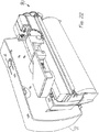
次に図3に目を向けると、該カメラシステムの組み立て体は、プラスチックで射出成形された部品である内部シャーシ12に組み付けられている。カール矯正のために使用される一対のペーパーピンチローラ28,29は、例えば26,27に示すような対応するフレーム孔の中にスナップ止めされている。
【0071】
前記シャーシ12は、図4に示されるように、例えば13や14のような、一組の互いに対向する突起部を有しており、その内部には一組の電気モータ16,17がスナップ止めされている。それらの電気モータ16,17には、全く標準的なものを使用でき、モータ16はステッパモータタイプであり、一連のギヤ(gear wells)を駆動するための歯車部分(cogged end portion)19,20を有している。第1のギヤ(gear wells)セットはペーパー切断装置を駆動するためのもので、第2のセットはプリントロール動作をコントロールするためのものである。
【0072】
次に、図5〜7に目を向けると、そこにはそのカメラシステムにて使用されるインク供給装置40が示されている。図5は後面からの分解斜視図を示し、図6は後面からの組み立て図を示し、図7は正面からの組み立て図を示す。そのインク供給装置40はインク供給カートリッジ42の周りに構築されており、該インク供給カートリッジ42は、要求に応じて写真をプリントアウトするためのプリンターインクやプリントヘッド装置を有する。そのインク供給カートリッジ42は、画像をペーパーロールから切るのを補助するための切断用帯としての側部アルミストリップ43を有している。
【0073】
ダイヤル装置44は、“プリント残り”の数を表示するために設けられている。そのダイヤル44は、回転自在となるように、対応する被係合部46にスナップ止めされている。
【0074】
図6に示すように、そのプリントヘッドはフレキシブルなPCBストリップ47を有しており、該ストリップは該プリントヘッドに接続され該プリントヘッドの制御を行うようになっている。フレキシブルなPCBストリップとイメージセンサーやプリントヘッドチップとの間の接続はTAB(Tape Automated Bonding)ストリップ51,58により行うことができる。また、成形された非球面レンズや絞りシム(図5)が、イメージセンサーチップの表面に画像を形成するために設けられている。該イメージセンサーチップは通常は空洞53の内部に配置されている。また、正確な光のコントロールを実行するため、前記空洞53を閉塞するように、光の箱モジュール(light box module)又はフード52がスナップ止めされている。例えば34のような、一連のデカップリング・コンデンサもまた配置されている。さらに、プラグ45(図7)が、補給後にインク孔を塞ぐために配置されている。さらに、フレキシブルPCBストリップ47をガイドするために、例えば、55−57に示すような、一連のガイド用突起が配置されている。
【0075】
前記インク供給装置の内部に配置されたプリントヘッドの下側にはプリントメディアがプラテンユニットにより搬送されるようになっており、該インク供給装置は該プラテンユニットと相互に作用し合う。図8は、そのプラテンユニット60の分解図を示し、図9及び10は、そのプラテンユニット60の組み立て図を示す。このプラテンユニット60は、プラテンベース62の一側にスナップ止めされた第1ピンチローラ61を有する。そのプラテンベース62の他側に取り付けられているのは切断機構63である。プラテンベース62に同様に取り付けられた歯車65により、螺旋状のネジを有するロッド64が回転され、それにより、前記切断機構63がプラテンに沿って横移動するように構成されている。その螺旋状のネジにはブロック67が係合されており、該ブロック67は、締め具69により締め付けられるカッティング円板68を有している。また、そのブロック67には、突起71を有するカウントアクチュエータも取り付けられている。該突起71は、カッティング円板68が戻ってくるときに図6のダイヤル装置44を回転させる。既に図6にて示されているように、前記ダイヤル装置44は歯車面(cogged surface)を有しており、該歯車面は前記ポール・レバー73に接触する。それによって、ダイヤル装置44の表面に表示された写真の枚数が保持される。前記切断機構63は、例えば、ソケット部(receptacle)74によるスナップ止めという方法でプラテンベース62に挿入される。
【0076】
プラテンベース62は、使用されていないときのプリントヘッドに蓋をする内部蓋装置80を備えている。該蓋装置80は、スポンジ部分81を有しており、プリントヘッドの蓋をするようにソレノイドコイルにて駆動される。好ましい実施形態においては、インクジェットプリントヘッドの蓋をするプリントヘッド蓋装置であって、携帯型カメラシステムに組み込まれるものが安価に提供される。
【0077】
図11は、該蓋装置の分解図を示し、図12はその端部の拡大図を示す。該蓋装置80は、絶縁線からなる16巻きコイル75を有するソレノイドの周りに構築される。前記プラテン62(図8)の底面に第1の固定ソレノイドアーム76が取り付けられ、該ソレノイドアーム76は、駆動の効果を増幅させるためのポスト部77を備え、前記コイル75は、第1の固定ソレノイドアーム76の周りに巻き付けられている。該アーム76は鉄鋼材により形成することができる。
【0078】
該ソレノイドアクチュエータにおける第2の可動アームは符号78で示される。該アーム78は移動可能で、鉄鋼材料からなる。該アームに取り付けられたスポンジ部分はエラストマー・ストリップ79により囲まれている。そのエラストマー・ストリップ79は、プリントヘッドインク供給カートリッジ42の表面をシールするために設けられたものであって、通常は弓状の断面形状であって、該プリントヘッドインク供給カートリッジ42(図5)の表面に対して板バネのように作用する。休止位置においては、エラストマー・スプリングユニット87,88は、インク供給ユニット42の表面をエラストマーシール79が弾性的に付勢するようにする。
【0079】
プリントヘッドユニットを駆動したいときには、紙を差し込んだ上で、ソレノイドコイル75を駆動し、アーム78をエンドプレート77に近接するまで下降させる。プリントヘッドがプリントしている間、アーム78は、コイル77中を流れる微小の保持電流によってエンドプレート76に密着されている。該保持電流が駆動電流よりもかなり小さくても同様の結果が得られる。その後、写真をプリントした後に、図8に示す切断機構63が図5に示すアルミストリップ43に接触するように駆動されることによってその写真紙が裁断される。そして、蓋装置88のエリアを掃除するように巻かれる。その後、電流がオフにされ、前記スプリング87,88が前記アーム78を元に戻し、前記エラストマーシールが前記プリントヘッドインク供給カートリッジに再接触される。
【0080】
好ましい実施形態では、長い長方形状のソレノイドタイプのデバイスの利用により、単純で安価なプリントヘッド蓋装置が提供される。さらに、好ましい実施形態では、電流は、装置が駆動されている間だけ必要とされ、プリントヘッドがプリントをしている間は低い保持電流のみが必要とされるという、低電力が使用される。
【0081】
次に、図13及び図14に目を向けると、図13はインク供給カートリッジ42の分解斜視図を示し、図14は、所定の位置にプリントヘッドユニットを有するインク供給カートリッジの底部の拡大断面図を示す。インク供給カートリッジ42は、ページ幅のプリントヘッド102のそばに構築されている。このプリントヘッド102はシリコンの長いスライサーを有しており、該スライサーは、射出されるインクをシリコンウエハの正面に供給するための一連の孔をその背面に備えている。これらの孔はマイクロメカトロニカルシステムで形成される。射出の形態としては、別表の関連仮特許明細書中に示されているような多くの異なる形態がある。特に、本件と同時に出願された“画像作成方法及び装置(IJ38)”と名付けられた仮特許明細書に明記されたインクジェットプリントシステムは極めて好適である。もちろん、別表に示すように、多くの他のインクジェット技術もまたプリントヘッドユニット102を構築する場合に利用され得る。前記インク供給カートリッジ42の基本的な要求は、前記プリントヘッド102の背面に形成された一連の色通路にインクを供給することである。その好適な実施形態の説明において、フルカラー写真が出力されるように、3色のプリント工程が使用されるべきであることを前提としている。それ故に、プリント供給ユニット42は、シアン容器104、マゼンタ容器105及びイエロー容器の3つのインク供給用容器を有する。それぞれの容器は、インクを蓄えておくことを要求され、スポンジ状材料107−109を配置して、インク供給路にインクを安定供給し、プリントヘッドが稼動される際にインクが前後に跳ねることを防ぐようにしている。容器104,105,106は、第2のベースピース111と合体される第2の外側プラスチックピース110の合わせ部(mating)に形成される。
【0082】
該ベースピース111の第1端には一連の空気吸入口113−115が形成されている。それらの空気吸入口は曲がりくねった通路に連通されており、該通路は、インクを寄せ付けないように疎水処理されている。さらに、その通路は、チャンバー104−106からのインクの流れ出しを防ぐために渦巻き型の通路を形成している。粘着性のテープ部117が端部(end portion)118に通路を密封するために貼り付けられる。
【0083】
(インク供給カートリッジの)上端には、インク供給チャンバー104,105,106に(インクを)補充するための一連の補充孔が形成されている。該補充孔はプラグ121により封止されている。
【0084】
図14に目を向けると、そこには、ユニットとして構成される図13のインク供給カートリッジ42の断面を部分的に拡大した斜視図が示されている。そのインク供給カートリッジ42は3個のカラーインク容器104,105,106を有しており、それらの容器はプリントヘッド102の背面の異なる部分にインクを供給するものであって、該プリントヘッド102は、前面へのインクの供給するための一連の隙間128を有する。
【0085】
前記インク供給ユニットは、インクチャンバーを分離する2つのガイドウォール124,125を有している。それらのガイドウォール124,125は、プリントヘッド102の表面に接する端部にかけて次第に細くなるように形成されている。該ガイドウォールはさらに、例えば126のブロック部によって左右対称に機械的に補助されている。そのブロック部126は、プリントヘッド供給ユニットの長手方向に沿って均一な間隔で配置されている。それらのブロック部126は、プリントヘッド102の背面にインクを供給するために、該背面に近接する部分に空隙を残している。
【0086】
前記プリントヘッド供給ユニットは、好ましくは、多部分に分かれた、プラスチック射出成形モールドから形成される。そのモールド片(例えば、図13の110,111)は前記スポンジ片107,109を囲むようにスナップ結合される。次に、注射器型の装置がインク補充孔に挿入され、インク容器にインクが充填される。このとき、空気排出口113−115からは空気が流れ出る。次に、粘着性のテープ部117とプラグ121とが装着され、プリントヘッドの駆動がテストされる。(上述のようなインク容器への)インクの供給は、前記インク供給カートリッジを(カメラシステム本体から)取り外し、洗浄サイクルを実行し、そして、前記インク補充孔にインク補充用注射器を挿入することによって行うことができる。
【0087】
図15に目を向けると、そこにはイメージ・キャプチャー・プロセッシング・チップ(ICP)48のレイアウトの一例が示されている。このイメージ・キャプチャー・プロセッシング・チップ48は、プリントヘッドチップを除いた、カメラにおける電子的機能のほとんどを提供している。そのチップ48は高度集積システムである。それは、CMOSイメージセンシングや、アナログデジタル変換や、デジタルイメージ処理や、DRAMストレージや、ROMや、種々雑多なコントロール機能を1つのチップの中に一体化させている。
【0088】
そのチップは、最先端の0.18ミクロンのCMOS/DRAM/APSプロセスを使って、約32mm2を実現している。そのチップサイズとコストはムーアの法則で幾らか低減することができるが、CMOSアクティブ画素センサー配列201により左右される。したがって、チップサイズやコストの低減は、回折限界に取り組むセンサー画素として限界がある。
【0089】
そのICP48は、CMOSロジックと、CMOSイメージセンサーと、DRAMと、アナログ回路とを有する。非常に小容量のフラッシュメモリーや,他の不揮発性メモリーが好ましくはリバース・エンジニアリング(分解による模倣)から保護するために含まれている。
【0090】
別の方法として、ICPを単純に2つのチップに分割することができる。;1つはCMOSイメージング・アレイのためのもので、他は回路維持のためのものである。このように2つのチップを用いる場合のコストは、単チップのICPの場合のコストと大きくは変わらない。その理由は、パッケージや接着部のための余分な費用が、カラーフィルター製造工程で必要なウエハ面積の減少により幾分か相殺されることによる。そのICPは好ましくは、次の機能を有する。
【表1】

CPU、DRAM、イメージセンサー、ROM、フラッシュメモリー、パラレル・インターフェース、JTAGインターフェース、及びA/Dコンバータは、ベンダーにより供給されたコアにすることができる。該ICPは、2本の単三電池だけで簡単に駆動することができ、1.5Vで最小限の電力消費で駆動されるものである。
【0092】
図15は、ICP48の配置を示す。ICP48は、そのチップ面積の約80%をイメージング・アレイ201が占めている。そのイメージング・アレイは1,500×1,000の解像度を有するCMOS 4トランジスタ・アクティブ画素設計である。そのアレイは、2つのG画素と1つのR画素と1つのBからなる定型的な配置(それらが1つの画素群を構成する)に分割されることができる。そのイメージング・アレイには750×500の画素群がある。
【0093】
イメージセンサーや一般的なCMOSイメージセンサー分野における最近の進歩は、1997年10月のIEEE Transactions on Electron Devices、特に、1689頁から1968頁に見い出すことができる。さらに、本出願に開示されているのと同様の明確な実施(implementation)は、「ウォンらによる“1.8V,0.25μmのCMOS技術によって製造されるCMOS アクティブ画素イメージセンサー”、IEDM 1996年、915頁」に開示されている。
【0094】
そのイメージング・アレイは、標準的な配置である、4トランジスタ・アクティブ画素設計を使用している。チップ面積を小さくしてコストを抑えるため、イメージセンサー画素は科学技術の利用で実現可能な程度に小さくすべきである。4トランジスタ・セルによれば、典型的な画素サイズはリソグラフィを用いた場合のサイズの20倍も削減できる。これにより、約3.6μm×3.6μmの最小ピクセル面積を達成できる。しかしながら、フォトサイトはレンズの回折限界を大幅に上回るに違いない。また、四角のフォトサイトを有すること、水平方向及び垂直方向の両方向に回折限界を超えたマージンを最大にすることは、都合良い。このケースでは、フォトサイトは、2.5μm×2.5μmの仕様にすることができる。そのフォトサイトは、フォトゲートや、ピンフォトダイオードや、チャージ変調装置や他のセンサーにすることができる。
【0095】
画素とフォトサイトの両方を四角に配置するために、4つのトランジスタは、長方形状ではなくむしろ’L’字状に配置される。このような配置は、トランジスタの実装密度を僅かに減少させ、画素サイズを大きくしてしまう。しかしながら、回折限界を回避する方が実装密度の僅かな減少よりもメリットがある。
【0096】
それらのトランジスタは、また、前記処理技術にとっての最小値よりも長いゲート長を有している。これらは、0.18ミクロンの延伸長から0.36ミクロンの延伸長に増加している。このことで、ゲート長に変化を付けることによるトランジスタのマッチングが、総ゲート長の内の小さな割合を示すことが好転する。
【0097】
余分のゲート長、及び‘L’字状の実装は、その技術にとって、トランジスタが最小よりも少々面積を使うことを意味する。普通は、8μm2前後が長方形配置のために必要とされる。多分、9.75μm2がトランジスタのために許容される。
【0098】
各画素の総面積は16μm2であり、4μm×4μmの画素サイズである。1,500×1,000の解像度では、イメージング・アレイ101の面積は6,000μm×4,000μm、或いは24mm2である。
【0099】
該チップにおけるカラーイメージセンサーの存在は、主に2つの点で、要求されるプロセスに影響を与える。すなわち、
− CMOS製造プロセスが暗電流を最小化するのに最適化されるべきである。
− カラーフィルターが必要とされる。これらは、着色された感光性ポリイミドを使用し、3層のスピンコーティングと、3つの乾燥工程とにより作製される。
【0100】
1,500のアナログ信号プロセッサ(ASPs)205がある。1つのプロセッサは、各センサーの列のためにある。それらのASPsはその信号を増幅し、暗電流の参考値や、サンプル及びホールド信号を与え、固定パターンノイズ(FPN)を削除する。
【0101】
375個のアナログデジタルコンバータ206がある。1つのコンバータは、4つのセンサー列のためにある。これらはΔΣ型、或いは逐次比較型のアナログデジタルコンバータかも知れない。アナログデジタルコンバータの列は、要求される変換速度の減少、並びに、信号がデジタルに変換される前に受ける、アナログ信号の低下量の減少のために使用される。また、これは、ホットスポット(局所的な暗電流に影響を与える)や、シングルハイスピードのアナログデジタルコンバータが使用された場合に発生するノイズが生じた基板を除去する。1つのアナログデジタルコンバータは2つの4ビットDACを有する。DACは、カラム間のFPN変化をさらに減少させるため、ADCのオフセットやスケールを取り除く。これらのDACは、チップテストの間にフラッシュメモリーに格納されたデータにより制御される。
【0102】
カラム選択ロジック204は1:1500のデコーダである。該デコーダは、出力バスに、ADCの適当なデジタル出力をイネーブルする。各アナログデジタルコンバータには4つの列に割り当てられているので、ロー選択コントロール4の内の少なくとも重要な2ビットはアナログマルチプレクサに入力される。
【0103】
ローデコーダ207は、アクティブ画素センサー配列の適切な列(ロー)をイネーブルする1:1000デコーダである。これは、イメージング・アレイの1000列の内、アナログ信号プロセッサーに接続されているものを選択する。それらの列は順番に常にアクセスしているので、列選択ロジックはシフトレジスタとして実行されることができる。
【0104】
自動露光システム208は、前のフレーム周期の間に検知した最大強度に応じてADC205の基準電圧を調節する。グリーン画素からのデータはデジタルピーク検出器を通り抜ける。キャプチャー(参考フレーム)前の画像フレーム周期のピーク値は、カラムADCのために広範囲の参考電圧を発生するDACに与えられる。そのピーク検出器は基準フレームの最初にリセットされる。また、RGBの3色の成分の最小値と最大値はまた色補正のために収集される。
【0105】
そのチップの2番目に大きな部分は、画像をホールドするために使用されるDRAM210に使用される。前記センサーからの1,500×1,000の画像を圧縮することなく格納するために、1.5MバイトのDRAM210が必要となる。これは、5メガビット、256メガビットの5%よりも僅かに小さいものに等しい。DRAM技術は、0.18μmのCMOSを使用して実行された256Mビット世代のものである。
【0106】
一般的な8Fセルを使用して、メモリアレイにより必要とされる面積は3.11mm2である。ローデコーダやカラムセンサや冗長(redundancy)や他の因子が考慮されたとき、DRAMは約4mm2必要とする。
【0107】
もし、写真をプリントする際の2秒間、CMOSイメージング・アレイにおいて画像信号のアナログストレージが正確に維持することができるならば、このDRAM210はたいていは削除することができる。しかしながら、劣化なしに保存でき、ノイズに強く、写真のコピーをかなり後にすることも可能であるという点で、画像のデジタルストレージが好ましい。
【0108】
DRAMアドレス発生器211は、書き込み及び読み込みアドレスをDRAM210に与える。通常の操作の下では、書き込みアドレスは、CMOSイメージセンサー201から読み込まれたデータの順番により決定される。これは概して単純なラスター方式にするだろう。しかしながら、もし、DRAMへの書き込みアドレスのマッチングが発生されたなら、任意の順序でセンサー201からデータを読み込むことができる。DRAM210からの読み込み順序は、通常は色補正やプリントヘッドの要求に単純に合わせる。ノズルアクチュエータのためにスペースを空けるため、プリントヘッドのシアンやマゼンタやイエローのロウ(行)は数画素分だけオフセットさせることが必要となるので、それらの色はDRAMから同時には読み込まれない。しかしながら、プリント工程の間、DRAMから全てのデータを読み込むための多くの時間が何回もある。この可能性はプリントヘッド・インターフェースにてFIFOの必要を削除するために使用され、それによってチップ面積を削減できる。全てのRGB3色の画像成分は、色データが必要とされる度にDRAMから読み込むことができる。このことは、RGBからCMYへの単純な線形変換よりも、より洗練された変換を行う色空間変換器を提供するものである。
【0109】
また、ラインバッファを必要とせずにイメージデータの2方向フィルタリングを許容するため、データがDRAMアレイから再読み込みされる。
【0110】
そのアドレス発生器は、また、カメラの一部のモデルにおいて映像効果を実行するかも知れない。例えば、パスポート用写真は、DRAMに読み込まれるアドレスの操作により作り出される。また、画像フレームの効果(画像の中央が減少)や、画像のゆがみや、万華鏡のような効果は、DRAMの読み込みアドレスの操作により全て発生させることができる。
【0111】
標準的なチップに効果が組み込まれたなら、そのアドレス発生器211はかなりの複雑さで使用されるかも知れないけれども、該アドレス発生器は、アドレスカウンターと、まあまあの量のランダム論理を有しているに過ぎないので、該アドレス発生器のために使用されるチップ面積は小さい。
【0112】
色補間214は、1個のR画素と2個のG画素と1個のB画素とが交互に配置されたパターンをRGBの画素に変換する。それは、3個の8ビット加算器と、関連レジスタとからなる。その分割(division)は、2(緑用)か4(赤及び青用)により、加算機の出力連結部に固定された変動として使用されることができる。
【0113】
コンボルバー215は、画像の赤や緑や青の面に小さなコンボリューション・カーネル(convolution kernel)(5×5)を与えるシャープニング・フィルタとして用意される。多くのサンプルにおいて緑は2倍あるので、緑の面のためのコンボリューション・カーネルは、赤や青の面のためのカーネルとは異なる。そのシャープニング・フィルタは5つの機能を有する。すなわち、
− 前記色補間によって提供された線形補間(linear interpolation)をsinc interpolationに近似する色補間に改良すること
− デジタル処理によって発生する、画像の‘softening’を補償すること
− 平均的な消費者の好み(実際よりも僅かにシャープな画像)に合わせるように画像のシャープネスを調整すること。1回使用のカメラは消費財であって、プロ用の写真製品ではないので、その処理は、むしろ最も正確にするよりも、最もポピュラーなセッティングにされる。
− 高周波ノイズ(個々の画素)のシャープニングを抑制すること。その機能は、‘アンシャープマスク’処理に似ている。
− 画像のゆがみのアンチエイリアス処理を行うこと
【0114】
これらの機能は全て1つのコンボリューション行列に結集されている。ピクセルレート(pixel rate)は1Mpisel/sよりも低いので、3つの色成分により要求される掛け算の総数は、1秒当たり5600万である。これは1つの乗算器によって実行することができる。係数ROMの50バイトが、また必要とされる。
【0115】
カラーALU113は色補正機能と色空間変換機能を1つのマトリックスの乗算に結合する。それは、フレームの各画素に与えられる。シャープニングを伴うので、色補正は、正確さよりも一般的なセッティングに合わせるべきである。
【0116】
カラーALUの色補正回路は、写真の明るさを補償する。写真の大部分は、3つの色成分の内のコントラストを明るさとを独立に正常化する、1色の補正により十分に改善される。
【0117】
カラー参照テーブル(CLUT)212はそれぞれの色成分のために準備されている。これらは、3つに分離された256×8SRAMであり、合計6,144bitを必要とする。そのCLUTは色補正プロセスのい一部として使用される。また、それらは、確率的に選択された‘ワイルドカラー’効果のような色の特殊効果のために使用される。
【0118】
カラーALUの色空間変換システムは、イメージセンサーのRGB色空間をプリンタのCMY色空間に変換する。最も簡単な変換はRGBデータの1つの補充である。しかしながら、この単純な変換は、両方の色空間の線形性の完璧さ、及び、イメージセンサーのカラーフィルターやインク染料の色スペクトルの完璧さが必要とされる。サンプルの3次元自由変換テーブルのトリ・リニアー補間は、それとは正反対である。これは、他の色空間において、非線形性、或いは違いを効果的にマッチすることができる。そのようなシステムは、印刷エンジンが色電子写真である場合に、優れた色空間変換を得るために必要である。
【0119】
しかしながら、ハーフトーンのインクジェット出力の非線形性は大変小さいので、より簡単なシステムを使用することができる。簡単なマトリクスの掛け算が素晴らしい結果をもたらすことができる。これにより、contone画素につき9つの掛け算と6つの足し算とが必要となる。しかしながら、contone画素の速度は遅い(1Mピクセル/秒以下)ので、これらの操作は1つの乗算器及び加算機に分けることができる。その乗算器及び加算機は、色補償機能を有するカラーALUに使用されている。
【0120】
デジタルハーフトーニングは、確率論的な、最適化されるディザセルを使用する、分散されるドットを整理するディザとして形成されることができる。ハーフトーン・マトリックスROM116はディザー・セル係数を格納するために用意される。32×32のディザー・セルサイズは、セルの繰り返しサイクルが見えないことを確実にするために適合される。インクドットの位置を最大限に確かにするため、3色−シアン、マゼンタ、及びイエロー−は、全て、同じセルを使ってディザ(dithered)される。これにより、まだ湿っている1つのドットから近接ドットへ染料のにじみを引き起こす、中間調の‘マディイング’が最小になる。1つのROMが3色それぞれのハーフトーンユニットに分割されるので、必要とされるROMの総サイズは1キロバイトである。
【0121】
使用されたデジタルハーフトーニングは、確率論的な、最適化されるディザ・マトリクスで順序付けられたディザに分散される。ディザリングは、誤差拡散のために画像をあまりシャープにはしないけれども、不自然さを少しだけ伴っただけの、より正確な画像を生成することができる。誤差拡散により生成された画像のシャープさは人為的であり、contone domainにて行われる‘アンシャープ・マスク’のフィルタリングよりもコントロールできず、正確でもない。高いプリント解像度(1,600dpi×1,600dpi)は、適切に形成された確率論的ディザ・マトリクスを使用したとき、素晴らしい品質をもたらす。
【0122】
デジタルハーフトーニングは、デジタル・ハーフトーンユニット217により、DRAM210からのcontoneインフォメーションとディザ・マトリクス216のコンテンツとの単純な比較を行って達成できる。ハーフトーンプロセスの間、画像の解像度は、キャプチャーされたcontoneの画像の250dpiからプリントされた画像の1,600dpiに変化する。各contoneの画素は、平均40.96ハーフトーン・ドットに変換される。
【0123】
ICPは、ボタンの読み取り、モータやソレノイドのコントロール、ハードウェアのセッティングや、補給ステーションの認証のような、種々雑多なカメラの機能を実行するために16ビットのマイクロコントローラーCPUコア219に組み込まれている。CPUにより要求される処理能力は非常にささやかで、幅広い種類のプロセッサ・コアが使用されることができる。全てのCPUプログラムが小さなROM220から実行される。外部プログラムは実行されないので、カメラのバージョン間のプログラムの互換性は重要ではない。2Mbit(256Kbyte)のプログラムやデータROM220がチップに含められる。ROMスペースのほとんどは、画像の輪郭のためのデータや、特殊カメラのためのフォントをあてがっている。そのプログラムの要求は重要ではない。1つのかなり複雑なタスクは、補給ステーションの暗号化認証である。ROMはビット毎にシングル・トランジスタを必要とする。
【0124】
フラッシュメモリー221が128ビットの認証コードを格納するために使用されるかも知れない。これにより、リバース・エンジニアリングが本質的に実行不可となるので、ROMに認証コードを格納するよりも高いセキュリティを提供することができる。そのフラッシュメモリーは、走査型プローブ顕微鏡や電子ビームを使用してもデータの読み取りが不可能となるように、第3レベルの金属(third level metal)によって完全に被覆されている。その認証コードは製造時にチップ内に格納される。少なくとも2つの他のフラッシュビットが認証プロセスのために必要とされる。すなわち、1つのビットは認証コードの再プログラミングさせないようにするもので、もう1つのビットは、信頼できる補給ステーションによってそのカメラが補給処理されたものであることを示すものである。また、そのフラッシュメモリーは、イメージング・アレイのためのFPN補正データを格納するために使用することもできる。加えて、パラメータを設計し直す位相ロックループが、クロックサイクルを正確な時間にするために設けられている。そのクロック周波数は、データファンクションが与えられていないので、クリスタルのような正確さは望めない。クリスタルのコストを削除するため、位相ロックループ124を伴ったオンチップオシレータが使用される。オンチップオシレータの周波数がチップからチップへ大きく変化するので、PLLへのオシレータの度数比は、初期テストの際にデジタル処理で修正される。その値はフラッシュメモリー121に格納される。これにより、クロックPLLは、インクジェットプリンタのパルス幅を十分な正確さでコントロールすることができる。
【0125】
スクラッチパッドSRAMは、6Tセルを有する小さなスタティックRAM222である。そのスクラッチパッドは16ビットCPUのための一時メモリーとなる。1024バイトが適切である。
【0126】
プリントヘッド・インターフェース223はプリントヘッドのためにデータを正確にフォーマットする。また、そのプリントヘッド・インターフェースは、プリンタヘッドにより要求される全てのタイミング信号を提供する。これらのタイミング信号は温度や、同時にプリントされるドットの数や、プリントロールのプリントメディアや、プリントロール中のインクの染料濃度に応じて変化するかも知れない。
【0127】
次の表は、前記プリントヘッド・インターフェースへの外部接続の表である。
【表3】
フラッシュメモリー221が128ビットの認証コードを格納するために使用されるかも知れない。これにより、リバース・エンジニアリングが本質的に実行不可となるので、ROMに認証コードを格納するよりも高いセキュリティを提供することができる。そのフラッシュメモリーは、走査型プローブ顕微鏡や電子ビームを使用してもデータの読み取りが不可能となるように、第3レベルの金属(third level metal)によって完全に被覆されている。その認証コードは製造時にチップ内に格納される。少なくとも2つの他のフラッシュビットが認証プロセスのために必要とされる。すなわち、1つのビットは認証コードの再プログラミングさせないようにするもので、もう1つのビットは、信頼できる補給ステーションによってそのカメラが補給処理されたものであることを示すものである。また、そのフラッシュメモリーは、イメージング・アレイのためのFPN補正データを格納するために使用することもできる。加えて、パラメータを設計し直す位相ロックループが、クロックサイクルを正確な時間にするために設けられている。そのクロック周波数は、データファンクションが与えられていないので、クリスタルのような正確さは望めない。クリスタルのコストを削除するため、位相ロックループ124を伴ったオンチップオシレータが使用される。オンチップオシレータの周波数がチップからチップへ大きく変化するので、PLLへのオシレータの度数比は、初期テストの際にデジタル処理で修正される。その値はフラッシュメモリー121に格納される。これにより、クロックPLLは、インクジェットプリンタのパルス幅を十分な正確さでコントロールすることができる。
【0129】
スクラッチパッドSRAMは、6Tセルを有する小さなスタティックRAM222である。そのスクラッチパッドは16ビットCPUのための一時メモリーとなる。1024バイトが適切である。
【0130】
プリントヘッド・インターフェース223はプリントヘッドのためにデータを正確にフォーマットする。また、そのプリントヘッド・インターフェースは、プリンタヘッドにより要求される全てのタイミング信号を提供する。これらのタイミング信号は温度や、同時にプリントされるドットの数や、プリントロールのプリントメディアや、プリントロール中のインクの染料濃度に応じて変化するかも知れない。
【0131】
次の表は、前記プリントヘッド・インターフェースへの外部接続の表である。
【表4】
使用するプリントヘッドは、8個の等しいセグメント(それぞれは1.25cmの長さ)から成る。それらのセグメントの接続は、プリントヘッドチップ上では行われず、外付けの両面TABボンディングフィルムにより行われる。8個の等しいセグメントへの分割は、ウエハステップが使用するリソグラフィを単純化する。1.25cmのセグメント幅はステッパー・フィールドに簡単にフィットする。プリントヘッドは長くて狭いので(10cm×0.3mm)、ステッパー・フィールドは、32プリントヘッドチップの1つのセグメントを含む。したがって、ステッパー・フィールドは1.25cm×1.6cmである。4つの完全なプリントヘッドの平均は各ウエハステップでパターニングされる。
【0133】
これは、画質に影響を与える電圧フリッカやホットスポットを回避することである。さらに、トランジスタはセンサーから出来るだけ離して配置される。
【0134】
標準的なJTAG(Joint Test Action Group)インターフェース228は、テストの目的のため、補給ステーションによる認証のためにICPの中に含められる。チップの複雑さのせいで、BIST(内蔵自己試験機能)や機能のブロック・アイソレーションを含む、様々なテスト技術が必要とされる。チップ面積の10%以上は、ランダム論理部のためのチップテスト回路として使われる。広い配列(イメージセンサーやDRAM)の諸経費は少ない。
【0135】
JTAGインターフェースは、また、補給ステーションの認証のために使用される。このようにすることにより、適切に構成された補給ステーションにて、良質な紙やインクのみがカメラに補給されることが確実となり、品質の悪い補給がなされないようにされる。そのカメラは、補給ステーションを(その逆よりはむしろ)証明しなければならない。自動的なテスト手順が実施されている間、保護プロトコルがその補給ステーションと通信する。新たなインクがプリントヘッドに補充されると、その補給ステーションによってICPプリントヘッドTAB上の4つの金メッキポイントに接続される。
【0136】
図16は製造工程における次のステップの背面図を示し、図17はカメラの正面からの図を示す。
【0137】
図16に目を向けると、カメラシステムの組立体は、まずインク供給装置40を組み付けることから着手される。フレキシブルPCBが、プラスチック型86に巻き付けられたプリントロール85の中空部に挿入されている複数の電池(符号84で示すように、1つだけが図示されている)に接続される。エンドキャップ89は、プリントロールと電池とがインク供給装置にしっかりと固定されるようにプリントロール85の他端に設けられる。
【0138】
前記フレキシブルPCBの電気接点には、図8に示す板バネ97,98の端部が接続され、さらに、該板バネにはソレノイドが接続されて、ソレノイドが電気的に制御されるようになっている。
【0139】
次に、図17−19に目を向けると、製造工程の次のステップは、カメラシャーシの側部に適切なギヤを取り付けることである。図17はカメラの正面図を示し、図18は背面図を示し、図19もまた背面図を示す。歯車22,23からなる第1ギヤは、歯車23が歯車65(図8)に噛合されていて裁断ブレードを駆動するために使用される。歯車24,25,26からなる第2ギヤは、図8のプリントローラー61の一端に取り付けられている。図18に最も良く示されるように、それらの歯車は、シャーシ表面の対応する軸部(button)に嵌め込まれる。なお、歯車26は、対応する孔部27にスナップ止めされる。
【0140】
次に、図20に示されるように、組み立てられたプラテン・ユニットがプリントロール85とアルミカッティングブレード43との間に挿入される。
【0141】
次に、図21に目を向けると、イルミネーションの手段として、カメラシステムの電気的な双方向部品が示されている。既に述べたように、それらの部品はフレキシブルなPCB板に配置され、前記イメージセンサーや処理チップ51をプリントヘッド102に接続するTABフィルム58を有する。電力は2つの単三電池83,84から供給され、紙搬送用のステッパモータ16が回転裁断モータ20の他に配置されている。
【0142】
光学素子31は、シャーシ12の最上部に嵌め込むようにして配置される。その光学素子31は、ビューファインダー溝材37の被係合部35,36に係合されるオプティカル・ビューファインダー32,33を含む。また、その光学素子31には、外部ディスプレイ用に、LED5からの明かりを導くための光学用パイプ部材39に加え、プリントの残り枚数を拡大するためのレンズシステム38が配置されている。
【0143】
図22に戻って、組み立てられたユニット90は、プリントアウトの起動ボタン4を有するフロント・アウターケース91の中に挿入される。
【0144】
次に図23に目を向けると、前記ユニット90には、スロット6やコピープリントボタン7を有するスナップ式バックカバー93が取り付けられる。使用説明や広告が表示された帯状ラベル(不図示)が、そのバックカバーに貼り付けられ、フレキシブルなプラスチックやゴムのストリップからなるクランプ・ストリップ96がそのカバーに取り付けられている。
【0145】
続いて、要求に応じてインスタントの出力画像を提供するという好適な実施形態が、1度だけ使用するカメラシステムのために用意されている。その好適な実施形態がさらに補給可能なカメラシステムを提供することは明らかだろう。使用されたカメラは、回収され、そのアウター・プラスチックケースが取り除かれ、再生されることができる。新しいペーパーロールや電池を補充し、インクカートリッジにインクを充填することができる。一連の自動テストの手順が、プリンターが適切に使用できることを裏付けるために実施される。さらに、品質を向上させるため、認証された補給のみが行われることを確実にするため、そのカメラが保護プロトコルを使って補給ステーションを認証するように、オンチップ・プログラム用ROMにおける手順が実行される。認証の後、そのカメラは、内部の紙のカウントがリセットされ、新しいラベルを貼ったアウターケースがカメラシステムに固定される。続いて、包装と出荷とが行われる。
【0146】
さらに、様々なデジタル処理手順を許容するように前記プログラム用ROMを変更できることは、当業者には明らかだろう。一般的な消費者の好みに最適化されるよう、デジタル処理で見栄えを良くした写真に加え、様々な他のモデルが、前記プログラム用ROMを単に再プログラムすることにより得ることができる。カラーマッピング機能をマッピングし直すことによって、例えば、セピアクラシックの古めかしいスタイルの出力を得ることができる。さらに別の場合、好適なカラーリマッピングアルゴリズムを通じて、白黒写真が得られる。また、白黒写真を着色して古めかしい効果を作り出すために、白黒のプリントに僅かな色を加えることもできる。さらに、パスポート写真の出力が、アドレス発生器にて好適なアドレスをリマッピングすることにより得ることができる。さらに、画像処理の分野で知られているように、エッジフィルタを使用して、スケッチしたようなアートスタイルを得ることができる。さらに、適切なクリップアートを付加して出力画像の周りに、伝統的な結婚式の縁やデザインを配置することができる。例えば、結婚式用のカメラが提供されるかも知れない。さらに、良く知られているパノラマ形式の画像を出力するようにパノラマモードを用意することもできる。さらに、送料を含む郵便葉書をプリントロールの裏面に印刷することにより、郵便葉書形式の出力を得ることもできる。さらに、ハロウィンやクリスマスなどのような特別のイベントのためにクリップアートを提供することもできる。さらに、アドレスをリマッピングすることにより万華鏡の効果を得ることができ、カラー・ルックアップテーブルのリマッピングにより自然色の効果を得ることもできる。特別なイベントのためのカメラ、例えば、オリンピックや、映画のタイアップや広告や、他の特別なイベントに専用のカメラを提供することができる。
【0147】
写真を撮るために(ボタンを)押し下げると、重要でないパラメータを決定するために最初の画像がセンサー配列によってサンプリングされるように、カメラの動作モードがプログラムされている。次に、出力のために使用される、二番目の画像が再びキャプチャーされる。そのキャプチャーされた画像は、最初にペーパーロールに出力される前の特別な要求に従って操作される。画像を保持するためにDRAMをリフレッシュする間、予め決められた時間だけLEDライトが駆動される。もし、この間にプリントコピーボタンが押されたなら、写真のさらなるコピーが出力される。カメラが使用されず、予め決められた時間が経過すると、再びシャッターボタンがオンにされるまで、カメラシステムへの全てのパワーをオンボードCPUが切る。この方法により、電力のかなりの節約を実現できる。
インクジェットプリンティング
相当数の新型のインクジェットプリンタが、好適な実施形態として、インクジェット技術に取って代わるために発展してきている。インクジェットデバイスの様々な組み合わせが、本発明の一部として開示されているプリンタデバイスの中に含めることができる。相互参照表により特別に示される、これらのインクジェットに関連するオーストラリアの仮特許の明細書がある。すなわち、
【表5−1】
さらに、本出願は、多数のインクジェットプリンタの構築に、高度な半導体製造技術が使用されるかも知れない。好適な製造技術は、次の相互参照表に示されているオーストラリア仮特許の明細書中に開示されている。
【表6−1】
さらに、本実施例は、インクジェットヘッドへのインク配送システムを利用しても良い。一連のインクジェットノズルにインクを供給するための配送システムは、次の相互参照表に示されているオーストラリア仮特許の明細書中に開示されている。
【表7】
さらに、本願は、インクジェットプリンタの配列を行う際に高度な半導体マイクロエレクトロメカニカル技術(MEMS技術)を利用しても良い。好適なマイクロエレクトロメカニカル技術は、次の相互参照表に示されているオーストラリア仮特許の明細書中に開示されている。
【表8】
さらに、本願は、次の相互参照表に示されているオーストラリア仮特許の明細書中に開示されているような使い捨てカメラシステムを利用するようにしても良い。
【表9】
【0148】
さらに、本願は、次の相互参照表に示されているオーストラリア仮特許の明細書中に開示されているようなデータ配信システムを使用するようにしても良い。
【表10】
さらに、本願は、次の相互参照表に示されているオーストラリア仮特許の明細書中に開示されているアートカム型装置のようなカメラとデータ処理技術を使用するようにしても良い。
【表11−1】
【0149】
本発明の実施例はインクジェットプリンタ型装置を使用している。もちろん、多くの異なる装置を使用することができる。しかしながら、現在ポピュラーなインクジェットプリント技術は適していそうにも無い。
【0150】
サーマルインクジェットでの最も重要な問題は電力消費である。インク滴の射出のエネルギー効率が悪いことに起因し、高速のために必要な電力は約100倍である。インクを吐出させる蒸気泡を生成するために、水の迅速な沸騰を必要とするからである。水は大変高い熱容量を有していて、サーマルインクジェットの利用において過熱される。これは、電気の入力を運動の出力に変換するため、約0.02%の効率を必要とする。
【0151】
ピエゾエレクトリックインクジェットでの最も重要な問題はサイズとコストである。ピエゾエレクトリッククリスタルは適当な駆動電圧にて非常に小さなデフレクション(deflection)を有していて、それ故、各ノズルのために大きなエリアが必要となる。また、各ピエゾエレクトリックのアクチュエータは、分離した基板の駆動回路に接続されなければならない。このことは、300程度のノズルの電流制限においては重要な問題ではないが、19,200のノズルを有するページ幅プリントヘッドの製造には大きな障害となる。
【0152】
理想としては、使用されたインクジェット技術は、非公開のデジタルカラープリンティングや、他のハイクォリティでハイスピードでローコストのプリント利用が要求される。デジタル写真の要求に合わせるため、新たなインクジェット技術が創出されてきた。目的の特徴は次のものである。:すなわち、
低電力(10ワット未満)
高解像度性能(1,600dpi又はそれ以上)
写真クォリティの出力
低製造コスト
小サイズ(横切り幅が最小となるようにページ幅を調整する)
ハイスピード(<1頁当たり2秒)
【0153】
これらの特徴の全ては、後述するインクジェットシステムにより、異なるレベルの困難さで突破されることが可能である。45個の異なるインクジェット技術は、高ボリュームの製造のために幅広い選択を与えるよう、受け継ぐ者によって発展されてきた。これらの技術は、後に記載する表に示すように、本出願人に指定された分離された応用を形成する。
【0154】
ここに示されるインクジェットの設計(デザイン)は、電池で駆動される1回使用のデジタルカメラから、卓上のネットワークプリンタや業務用のプリントシステムまで、幅の広いデジタルプリントシステムに適している。
【0155】
標準の装置を使用して簡単に製造するために、前記プリントヘッドは、MEMS後処理法によって、モノリシックの0.5ミクロンのCMOSチップに設計される。カラー写真の応用のため、前記プリントヘッドは100mmの長さで、インクジェットのタイプに応じた幅を有する。最小のプリントヘッドはIJ38であり、幅は0.35mmで、35mm2のチップ面積を有する。そのプリントヘッドは19,200個のノズルとデータ及び制御回路を有している。
【0156】
インクは、射出成形されたプラスチック製のインク通路を経由して、プリントヘッドの背面に供給される。そのモールディングは50ミクロの特徴(features)が必要とされる。その特徴は、標準的な射出成型工具の中にリソグラフィでマイクロマシン加工されたインサートを使用して形成されることができる。インクは、ウエハの正面に形成されたノズル・チャンバーへ、ウエハを貫通するように形成された孔を通って流れる。そのプリントヘッドはTABによりカメラ回路に接続されている。
相互参照付きのアプリケーション
【0157】
次表は、最近出願された米国特許出願のガイドである。それらの出願は、これと共に一斉に提出され、特別なケースに言及するときに、その後の表で使用される参考を用いて検討されている。これらの出願は、また、対応する参考番号を有するオーストラリア仮特許出願(前述の表にて示されたような)のように出願されている。
【表12−1】
【0158】
個々のインクジェットノズルの基本動作に関する11個の重要な特徴が特定されてきている。これらの特徴は大体は直角(orthogonal)であり、したがって、11次元のマトリクスとして解明されることができる。このマトリクスの11軸のほとんどは、本出願人により発展された記入事項を含む。
【0159】
次の表は、インクジェットタイプの11次元の表の軸を形成する。
アクチュエータ・メカニズム(18タイプ)
基本動作モード(7タイプ)
補助のアクチュエータ(8タイプ)
アクチュエータの増幅及び改良方法(17タイプ)
アクチュエータの動き(19タイプ)
ノズル補給方法(4タイプ)
吸入口への逆流を制限する方法(10タイプ)
ノズルの掃除方法(9タイプ)
ノズルプレート構造(9タイプ)
滴の噴出方向(5タイプ)
インクタイプ(7タイプ)
【0160】
これらの軸により表示された完全な11次元の表は、インクジェットノズルに関し、369億の可能な形態を含む。様々なインクジェット技術においてそれらの全てが実現可能ではないけれども、数百万は実行可能である。可能な形態の全てを説明することは、明らかに非現実的である。その代わり、いくつかのインクジェットタイプが詳細に吟味されてきた。それらが、上述の、指名されたIJ01からIJ45である。
【0161】
他のインクジェットの形態は、11軸の1又はそれ以上に沿って代替となる形態に置き換えることにより、これらの45の例から直ちに導き出すことができる。IJ01からIJ45のほとんどは、何らかの現在利用できるインクジェット技術より上位である特徴を、インクジェットプリントヘッドに作り込むことができる。
【0162】
発明者に知られている先行技術例がある場合には、これらの1又はそれ以上が、下記の表の例の欄に示される。該IJ01からIJ45のシリーズはまた、例の欄にも示されている。幾つかのケースでは、プリンタが、1つ以上の特徴を共有する場合には、1つの表に1回以上示されるかも知れない。
【0163】
好適な応用は以下のものを含む。すなわち、家庭用プリンタ、オフィス用ネットワークプリンタ、短期用デジタルプリンタ、業務用プリントシステム、布用プリンタ、ポケットプリンタ、インターネットwwwプリンタ、ビデオプリンタ、医療用画像、大判プリンタ、ノート型パソコン用プリンタ、ファックス機、工業用プリントシステム、写真コピー機、写真現像店等。
【0164】
前述した11次元のマトリクスで関連付けられた情報が以下の表に示される。
【表13−1】
具体的な実施例で示されたような、本発明に対して多くの変化、及び/又は変更が、広く述べられた発明の範囲から逸脱しない状態で実行されることは、当業者によって認識されるだろう。したがって、そのような実施例は、あらゆる点で説明に役立ち、制限を受けないと見なされる。
【図面の簡単な説明】
【0164】
本発明の範囲に入る他の形態があるにもかかわらず、本発明の好ましい形態が、ほんの一例として、添付図面を参照して次のように開示される。
【0165】
【図1】 図1は、好適な実施態様である、組み立てられたカメラを側前方から見た斜視図を示す。
【図2】 図2は、好適な実施形態であって、側後方から見た斜視図(一部は分解されている)を示す。
【図3】 図3は、好適な実施形態における、シャーシの側面斜視図を示す。
【図4】 図4は、電気モータの差込みを示す、シャーシを側方から見た斜視図である。
【図5】 図5は、好適な実施形態におけるインク供給装置を示す分解斜視図である。
【図6】 図6は、好適な実施形態におけるインク供給装置の組み立てられた構造を示す、側方から見た斜視図である。
【図7】 図7は、好適な実施形態におけるインク供給装置の組み立てられた構造を示す、前方から見た斜視図である。
【図8】 図8は、好適な実施形態におけるプラテンユニットを示す分解斜視図である。
【図9】 図9は、プラテンユニットの組み立てられた構造を示す、側方から見た斜視図である。
【図10】 図10は、プラテンユニットの組み立てられた構造を示す斜視図である。
【図11】 図11は、好適な実施形態におけるプリントヘッドの蓋装置を示す分解斜視図である。
【図12】 図12は、好適な実施形態における前記蓋装置を示す、拡大された分解斜視図である。
【図13】 図13は、好適な実施形態におけるインク供給カートリッジを示す分解斜視図である。
【図14】 図14は、組み立てられた状態のインク供給カートリッジの内部断面を部分的に示す拡大斜視図である。
【図15】 図15は、好適な実施形態における、イメージ・キャプチャー・プロセッシング・チップのチップ配列の一形態を示す、模式的なブロック図である。
【図16】 図16は、好適な実施形態における組み立て工程を示す分解斜視図である。
【図17】 図17は、好適な実施形態における組み立て工程を示す前方からの拡大斜視図である。
【図18】 図18は、好適な実施形態における組み立て工程を示す側方からの斜視図である。
【図19】 図19は、好適な実施形態における組み立て工程を示す側方からの斜視図である。
【図20】 図20は、好適な実施形態におけるプラテンユニットの挿入を示す斜視図である。
【図21】 図21は、好適な実施形態における電気部品の接続を示す。
【図22】 図22は、好適な実施形態における組み立て工程を示す。
【図23】 図23は、好適な実施形態における組み立て工程を示す斜視図である。[0001]
[Technical field]
The present invention substantially relates to a disposable camera having an instant print function, and specifically discloses a low-cost disposable camera.
[0002]
[Background of the invention]
In recent years, “single use” disposable cameras are increasingly becoming products for the general consumer. Disposable camera systems currently on the market usually have a built-in film roll and a simplified gear that allows the film roll to traverse an imaging device (having a shutter and lens system). An apparatus. After using only one film roll, the user passes the camera system to the photofinishing center for processing. The film roll is removed from the camera system and processed, and the photo is passed to the user. The camera system can then be regenerated by incorporating a new film roll into the camera system, replacing damaged or mountable parts, and repackaging the camera system as required. In this way, a single use “disposable” camera is provided to the consumer.
[0003]
Recently, a portable camera device having an internal print head, an image sensor and a processing device (the image detected by the image sensor means is processed by the processing device and is immediately printed out by the printing means upon request). Suggested by the present applicant. The proposed camera system further discloses an internal “print roll” system that carries print media such as film (in which ink is supplied from the printing means for the printing process and images are printed). ing. It is further disclosed that the print roll can be removed and replaced from within the camera system.
[0004]
Unfortunately, such a system is unlikely to be made without significant cost, and an instant camera system that retains the high quality features (a considerable number of features) described above is available at a lower price. It is desirable.
[0005]
In particular, in any “disposable camera”, it is desirable that the disposable part be easily and quickly refilled so that the disposable camera can be quickly refilled and returned to the market.
[0006]
Furthermore, a simple means of storing the refill portion in a disposable camera system is desired so that they can be quickly refilled.
[0007]
Further, in such a camera system, it is desirable to include an ink cartridge for storing ink used for printing out an image.
[0008]
It would be desirable to provide an extremely low cost camera system with as high a quality as possible. In this respect, as already proposed, the camera system includes a mechanism for detecting an image and processing the detected image in addition to a mechanism for printing an image on a print medium by a print head system. Should. Furthermore, it is desirable to provide a system that is easy to use and has a compact arrangement of parts so that a camera system capable of disposable printing can be manufactured at low cost.
[0009]
In any form of single-use camera, it would be necessary to be able to profit from the remanufacturing process in order to 'reproduce (create more)' the process of remanufacturing used cameras. . Unfortunately, such remanufacturing may cause enormous damage due to improper ink or print media usage in the camera. In particular, improper use of such materials is of poor quality if the disguise is remanufactured as an “original product (an original product that is not a remanufactured product)” May produce a product. In this regard, although not the manufacturer's responsibility, the consumer will immediately blame the manufacturer for poor quality products, and the damage may not be eradicated.
[0010]
Therefore, it would be desirable to build a camera and replenishment process system that would provide consumers with a higher quality product and a higher level of quality assurance to solve these problems.
[0011]
In the field of photography, three important effects are highly relevant. The first is the difference between color and black and white. Most photographs are now color photographs, but in the field of black and white photography, there are still steep areas that are not important. In addition, traditional camera photos typically use sepia tones, and camera photos that look particularly traditional, especially for marriage photos, are still quite popular. It is therefore desirable to be able to select these different types of output so that the user can easily use any of the different output formats.
[0012]
In addition, it is desirable to make a single use camera system as versatile as possible so that a considerable number of different specialization effects can be obtained immediately upon request.
[0013]
Unfortunately, for a disposable camera, it is desirable to reduce the required power as well as the degree of functional complexity. In this respect, it is necessary to make the operation efficient and to make the user interface as simple as possible.
[0014]
Unfortunately, such a system is likely to be constructed only at great cost, and a cheaper construction of an instant camera system is desired that can maintain a substantial quality in the aforementioned arrangement.
[0015]
Furthermore, it is advantageous to provide an effective connection of subcomponents in the camera system.
[0016]
It is effective to provide a camera system having effective color correction or remapping capability for the entire range.
[0017]
Unfortunately, such a system is likely to be constructed only at great cost, and a cheaper construction of an instant camera system is desired that can maintain a substantial quality in the aforementioned arrangement.
[0018]
Furthermore, it is effective to provide effective connection of subcomponents in the camera system and effective driving of the movable parts in the camera system.
[0019]
Furthermore, it would be advantageous to provide an effective connection of subcomponents in the camera system.
[0020]
Furthermore, since the use of a lid device is proposed in a disposable portable camera system, it is desired to provide an extremely low-cost device that can be used for a low-cost disposable camera.
[0021]
Furthermore, it would be desirable to provide a simple structure for automatic picture counting in a disposable camera system.
[0022]
Unfortunately, such a system is likely to be constructed only at great cost, and a cheaper construction of an instant camera system is desired that can maintain a substantial quality in the aforementioned arrangement.
[0023]
An object of the present invention is to provide an efficient single use disposable camera system.
[0024]
In accordance with an aspect of the present invention, a core chassis; an ink cartridge unit attached to the core chassis and having an ink supply and a printhead unit; rotatably attached between both ends of the chassis and the print A print media roll adjusted for printing by the head unit; a platen unit mounted below the print head unit; and an image connected to the print head unit and for printing by the print head unit A portable device comprising: an image sensor and a control circuit adjusted to detect; and an outer casing for housing the chassis, the ink cartridge unit, the print media, the platen unit, and the circuit. The camera system is provided.
[0025]
The camera system preferably comprises a cutting unit configured to traverse the print media to separate the print media into separated images. The cutting unit can be attached to the platen unit, and the platen unit can further include a print head lid unit for capping the print head when not in use.
[0026]
The camera system may further include a series of pinch rollers for decurling the print media.
[0027]
According to a further aspect of the present invention, an image sensor for detecting an image; a processing device for processing the detected image; a print media supply device prepared for storing print media; and a print built in the camera system In a camera system, comprising: a print head for printing a detected image on a medium; and a portable power supply device connected to the print head, the sensor, and the processing device; By disposing the power supply device in the hole, a method for efficiently arranging the print medium and the power supply device is provided.
[0028]
The print medium and the power supply device are preferably stored in a detachable unit that is removable from the camera system. The print medium may be rotated around the power supply device when the camera system prints the detected image on the print medium. The portable power supply device includes at least one battery, and preferably includes two standard batteries having end portions connected to each other. As those batteries, AA (AA type) batteries can be used.
[0029]
In accordance with a further aspect of the present invention, a printhead ink supply unit is provided for supplying ink to a page width printhead. A plurality of holes for supplying ink to a series of ejection nozzles are formed on the first surface of the print head. The print head ink supply unit includes a plurality of long columnar chambers for storing ink, and one chamber supplies ink of each color. These chambers are approximately the same length as the print head and are arranged in close proximity to the first surface. There is a separation wall formed so as to be gradually thinned so as to separate the chambers, and the separation wall is formed so as to be gradually narrowed toward an end portion, and the print head extends along the first surface. It is arranged in the same length.
[0030]
The printhead ink supply unit may further include auxiliary members (ie, a series of regularly arranged structural auxiliary members) that support the separation wall in an initial state. The separation wall is a separate wall from the print head and can be formed of a unit molded by one injection. The separation wall is tapered so as to form a gap in the wall of the unit, and the gap is set so that the print head is inserted. The unit can be constructed by joining two plastic molded parts.
[0031]
The long columnar chamber can be filled with a sponge-like material to assist in use. The printhead preferably emits at least three colors to provide a full color output image.
[0032]
The unit can have a series of air passages for communicating each chamber to the outside air, and the air passages have an irregular path from the end on the chamber side to the end on the outside air side. Also preferably, the passage has a hydrophobic surface to avoid ink inflow. The passage may be formed in a member having an exposed surface such that an adhesive surface is attached to the unit and sealed.
[0033]
Each chamber may further have an opening formed in the wall for filling the chamber with ink and for inserting a refilling needle.
[0034]
In accordance with a further aspect of the present invention, a portion includes a series of air passages formed to communicate each chamber to the outside air, the air passages from the chamber side end to the outside air side end. A print head ink supply unit is provided.
[0035]
In accordance with further aspects of the present invention, an image sensor and processing device for detecting and processing images; a print media supply device provided for storage of print media; and detection on print media embedded in a camera system There is provided a camera system including a print head for printing an image, and an image sensor and a processing device including one integrated circuit chip including the following elements.
A processing unit for controlling the drive of the camera system
· Program ROM used by the processing unit
・ CMOS active pixel image sensor for image detection
Memory for storing images and related program data
A series of motor drive units each having a motor drive transistor for driving an external mechanical system in the camera system
-Printhead interface unit for driving the printhead to print the detected image
[0036]
The motor drive transistor is preferably arranged along one peripheral edge of the integrated circuit, and the CMOS pixel image sensor is arranged along the opposite peripheral edge of the integrated circuit.
[0037]
The image sensor and the processing device preferably further include a halftone unit for converting the detected image into a bi-level pixel element for printing by the print head. The halftone unit can use a dither operation and has a halftone matrix ROM used by the halftone unit when performing a halftone operation.
[0038]
In accordance with a further aspect of the present invention, a camera system having an ink supply and print media for printing out a sensed image is provided that provides a system for authenticating that the camera system has been refilled. The system includes replenishment means for supplying ink and print media to the camera system; a communication connection device on the camera system side configured to connect to a communication connection device on the replenishment station side; A camera system interrogation device stored in the system and configured to utilize a communication connection device on the supply station side to query the supply station to determine reliability. .
[0039]
The camera system interrogation device can be formed in an integrated circuit of a silicon chip housed in the camera system. The camera system interrogation device is formed on the same silicon chip as an image sensor for detecting an image. The communication connection device can be a JTAG interface of the chip. Preferably, the camera system interrogation apparatus includes a sensitive memory such as a flash memory made by covering the sensitive memory with a conductive metal plate.
[0040]
After determining the reliability of the replenishment station, the camera system interrogation apparatus can reset the value of the print counter indicating the remaining number of prints after being output by the camera system.
[0041]
According to a further aspect of the present invention, an image sensor device for detecting an image; a processing device for processing the detected image; a storage device for storing an image and a program used by the processing device; and a camera system A print medium incorporated in the print medium; a print head for printing the detected image on the print medium; a variable switch for storing the current state of the output type of the camera system; and a switch connected to the processing device And a portable camera system. The switch connected to the processing device has a number of initially set states, and the processing device detects the state of the switch and causes the print head to output a corrected image according to the state. It is configured.
[0042]
Preferably, the processing device is configured to output at least two images from the next group. That is, a standard color image emphasized by digital processing, a sepia image, a black and white image, a black and white image with a little color added, a multi-passport photo image, an image that looks like a sketch, and an outline Images, panoramic images, images with clip art, images with kaleidoscope effect, and images with corrected colors.
[0043]
The processing device and the switch can be formed in one integrated circuit device, and the integrated circuit device can be programmed by an external device having a switch that can be programmed from the outside. The camera system can also have a removable cover with information printed on the surface to indicate the type of effect.
[0044]
According to a further aspect of the present invention, an image sensor device for detecting and storing images; a processing device for processing the detected images; a print media supply device prepared for storage of print media; a camera; A camera system comprising: a print head that prints a detected image on a print medium built in the system; and a first button and a second button connected to the processing device, respectively. Using the first button to cause the image sensor device to detect an image and using the second button to cause the print head to print a copy of the image.
[0045]
Preferably, the use of the first button causes the detected image to be printed out on a print medium by the print head. In addition, the camera system may comprise an activation indicator such as a light emitting diode, wherein the activation indicator is driven for an initial time when the image sensor is first activated, and at least during its initial set time. The step of storing the detected image, the step of turning off the operation indicator after the end of the initial setting time, and the step of stopping the operation of the sensor device after the end of the initial setting time can be performed. Furthermore, if the second button is pressed, the initial setting time can be extended.
[0046]
According to a further aspect of the present invention, an image sensor device for detecting an image; a processing device for processing the detected image; a print media supply device prepared for storing print media for image printing; A page width printhead molding having a series of ink supply chambers for storing ink and a printhead for printing a sensed image on a print media housed in the print media supply device; A camera system comprising the sensor and a portable power supply device connected to the processing device, wherein the image sensor device is attached to the camera system by attaching the image sensor device to a surface of the print head molding. I will provide a
[0047]
Preferably, the printhead is in the form of a long strip with a TAB connection at least at one end. The image sensor comprises a rectangular integrated planar integrated circuit having another TAB connection along at least one end, a planar integrated circuit, and a print head connected to each other.
[0048]
Further preferably, the processing device includes a print head control device incorporated in the planar integrated circuit for controlling the drive of the print head.
[0049]
The connection may include a series of wires embedded in a non-conductive flexible sheet that is generally rectangular in shape, with the print head connected to one side and the planar integration. A circuit is attached to the opening in the sheet.
[0050]
Further, the camera system has a series of control buttons attached to the flexible sheet.
[0051]
In accordance with a further aspect of the present invention, in a camera system comprising: an image sensor device for detecting an image; a processing device for processing the detected image; and a print head for printing out the detected image Using the image sensor device to detect a first image, processing the first image to determine a color characteristic of the first detected image, and detecting the second image; Using a sensor device to provide a color correction method for the second image based on the color characteristics of the first sensed image, starting from the first image, and printing out the second image. A color correction method for a detected image printed out by the print head is provided.
[0052]
Preferably, the second detection image is detected within one second from the first detection image, and the processing step includes examining a luminance characteristic of the first image. The processing steps include determining a maximum brightness and an initial brightness of the first image and resetting the brightness of the second image.
[0053]
In accordance with a further aspect of the present invention, an image sensor device for detecting an image; a processing device for processing the detected image; a print media supply provided for storing a roll of print media for image printing A page width printhead molding having a series of ink supply chambers for storing ink and a printhead for printing a sensed image on a print media contained in the print media supply device; A portable power supply device connected to the head, the sensor and the processing device; a cutting device for cutting a portion of the print media containing the image; and a paper media supply for transporting the paper through the print head A first drive motor for driving the apparatus; To provide a camera system comprising a second drive motor for driving the cutting device for cutting the A.
[0054]
Preferably, each of the drive motors includes a gear chain mechanism for driving a corresponding device with a gear. The first drive motor can be a stepper motor, which is preferably driven by the print head in a mutually exclusive manner.
[0055]
Furthermore, each drive motor can be driven forward or backward when operating the camera system normally.
[0056]
In accordance with a further aspect of the present invention, an image sensor device for detecting an image; a processing device for processing the detected image; a print media supply provided for storing a roll of print media for image printing An apparatus; a page having a series of ink supply chambers for storing ink used in the print head, and a print head for printing a sensed image on a print medium housed in the print medium supply apparatus A width printhead molding; and a series of pinch rollers disposed in a transport path between the print media supply device and the page width printhead molding and transporting the paper that has passed through the printhead. Provide a camera system.
[0057]
Preferably, the number of print rollers is at least three and the print rollers provide a curl twist to the print media. The print roller is snapped to the camera system. Two of the print rollers can be attached to a first chassis to which the print head molding is similarly attached, and a third print roller can be attached to a removable platen device. The third print roller can be inserted between the other two print rollers and the platen snapped to the chassis.
[0058]
According to a further aspect of the present invention, an image sensor device for detecting an image; a processing device for processing the detected image; a print media supply device for supplying print media to a print head; and a camera system A print head for printing a detected image on a built-in print medium; a portable power supply device connected to the print head, the sensor and the processing device; between the print media supply device and the print head And a cutting device that cuts the print medium into sheets of a set size.
[0059]
More preferably, the cutting device is removable from the camera system. The cutting device is attached to the print media supply device and can be detached from the camera system together with the print media. The cutting device can be attached to the platen below the print head.
[0060]
In accordance with a further aspect of the present invention, a first fixed iron arm; a solenoid coil wound around the iron arm portion; biased toward the printhead structure substantially close to the first arm; A second movable arm configured to be configured; a series of membranes attached to the second movable arm to seal the printhead structure in a resting state; and “paper or film” as the membrane And a solenoid that directs the movable arm to be spaced from the surface of the printhead structure to be transported between and to print ink thereon. A print head lid device for capping a head structure is provided.
[0061]
Preferably, the membrane is elastically folded to contact the surface of the printhead structure. The membrane has two opposing elastomeric strips that are generally continuous by the length of the ink ejection portion in the printhead structure so as to surround the portion from which the ink is ejected.
[0062]
The solenoid has a winding of a conducting wire wound around the protruding portion of the first arm, and the length of the winding is substantially the same as the length of the print head structure. Further, the second movable arm is biased to contact the surface of the printhead structure. The solenoid drives the second arm so as to be in close proximity to the first arm by passing a first level of current and prints a second, significantly lower level of current. And hold in a state close to the first arm. The present invention is generally applied to portable camera devices.
[0063]
According to a further aspect of the present invention, an image sensor device for detecting an image; a processing device for processing the detected image; a print media supply device provided for storing the print media in a roll; A print head for printing a sensed image on a print medium built in the camera system; and a worm screw extended by the length of the sensed image to be printed, for cutting the sensed image to be printed And a cutting blade (cutting blade) attached to the worm screw and driven by the length of the detected image to be printed, thereby cutting the print media into sheet pieces. A camera system including a worm gear;
[0064]
The cutting blade may comprise a rotating wheel having a sharpened outer edge. The wheel with gears may have a usage sign printed on one side. Further, the worm gear has a lever arm, and the lever arm moves (the lever arm) contacts the geared print indicator by moving the worm gear by the length of the printed detection image. Rotate the indicator to show the current number of prints.
[0065]
The camera further includes a pawl device that forms a ratchet and interacts with the gear of the wheeled wheel print indicator. The pawl device and the lever arm have a flexible portion associated with the wheeled wheel print indicator.
[0066]
In accordance with a further aspect of the present invention, there is provided a timing device capable of generating a clock signal whose period varies in proportion to an input signal; and a storage device for storing a value of the input signal input to the timing device. In an integrated circuit type device, the timing after producing an integrated circuit type device for determining a timing parameter value for redesigning the timing device to generate a clock output pulse having a period of an initially set width. A method is provided that includes testing a device.
[0067]
The clock signal can be used to determine a pulse length for driving an actuator of an inkjet printing type apparatus. Ideally, the device is used in a camera system that can print on demand, the timing device provides a clock signal for the printing-type device, and the storage device includes a flash memory circuit in the printing device.
[Description of Preferred and Other Embodiments]
[0068]
Turning first to FIGS. 1 and 2 simultaneously, there is shown a perspective view of an assembled camera constructed in accordance with a preferred embodiment. 1 shows a perspective view seen from the front, and FIG. 2 shows a perspective view seen from the back. The camera 1 includes a
[0069]
When the camera system 1 is used up, it outputs a standard number of prints. In order to display the remaining number of prints, a print remaining
[0070]
Turning now to FIG. 3, the camera system assembly is assembled to an
[0071]
As shown in FIG. 4, the
[0072]
Turning now to FIGS. 5-7, there is shown an
[0073]
The
[0074]
As shown in FIG. 6, the print head has a
[0075]
A print medium is conveyed by a platen unit below the print head disposed inside the ink supply device, and the ink supply device interacts with the platen unit. FIG. 8 shows an exploded view of the
[0076]
The
[0077]
FIG. 11 shows an exploded view of the lid device, and FIG. 12 shows an enlarged view of its end. The
[0078]
A second movable arm in the solenoid actuator is indicated at 78. The
[0079]
When it is desired to drive the print head unit, the paper is inserted and the
[0080]
In a preferred embodiment, the use of a long rectangular solenoid type device provides a simple and inexpensive print head lid device. Furthermore, in the preferred embodiment, low power is used, where current is only required while the device is being driven and only low holding current is required while the printhead is printing.
[0081]
Turning now to FIGS. 13 and 14, FIG. 13 shows an exploded perspective view of the
[0082]
A series of air inlets 113-115 are formed at the first end of the
[0083]
At the upper end (of the ink supply cartridge), a series of replenishing holes for replenishing (ink) the
[0084]
Turning to FIG. 14, there is shown a perspective view in which the cross section of the
[0085]
The ink supply unit has two
[0086]
The printhead supply unit is preferably formed from a multi-part plastic injection mold. The mold pieces (for example, 110 and 111 in FIG. 13) are snap-coupled so as to surround the
[0087]
Turning to FIG. 15, an example of the layout of an image capture processing chip (ICP) 48 is shown. The image
[0088]
The chip is about 32mm using a state-of-the-art 0.18 micron CMOS / DRAM / APS process.2Is realized. The chip size and cost can be reduced somewhat by Moore's Law, but depends on the CMOS active
[0089]
The
[0090]
Alternatively, the ICP can simply be divided into two chips. One for the CMOS imaging array and the other for circuit maintenance. Thus, the cost in the case of using two chips is not significantly different from the cost in the case of a single chip ICP. The reason is that the extra cost for the package and the bond is somewhat offset by the reduction in wafer area required in the color filter manufacturing process. The ICP preferably has the following functions.
[Table 1]
The CPU, DRAM, image sensor, ROM, flash memory, parallel interface, JTAG interface, and A / D converter can be a core supplied by the vendor. The ICP can be easily driven with only two AA batteries, and is driven with a minimum power consumption at 1.5V.
[0092]
FIG. 15 shows the arrangement of the
[0093]
Recent advances in the field of image sensors and general CMOS image sensors can be found in the October 1997 IEEE Transactions on Electron Devices, especially pages 1689 to 1968. Furthermore, a clear implementation similar to that disclosed in this application is “Won et al.“ CMOS Active Pixel Image Sensor Manufactured with 1.8V, 0.25 μm CMOS Technology ”, IEDM 1996. , Page 915 ".
[0094]
The imaging array uses a standard arrangement, a 4-transistor active pixel design. In order to reduce the chip area and reduce the cost, the image sensor pixel should be small enough to be realized by using science and technology. With a four transistor cell, the typical pixel size can be reduced by as much as 20 times the size when using lithography. Thereby, a minimum pixel area of about 3.6 μm × 3.6 μm can be achieved. However, photosites must significantly exceed the diffraction limit of the lens. It is also convenient to have square photosites and maximize the margin beyond the diffraction limit in both the horizontal and vertical directions. In this case, the photosite can be specified to 2.5 μm × 2.5 μm. The photosite can be a photogate, pin photodiode, charge modulator or other sensor.
[0095]
In order to place both pixels and photosites in a square, the four transistors are arranged in a 'L' shape rather than a rectangular shape. Such an arrangement slightly reduces the mounting density of the transistors and increases the pixel size. However, avoiding the diffraction limit is more advantageous than a slight decrease in packaging density.
[0096]
The transistors also have a gate length that is longer than the minimum for the processing technology. These increase from a stretch length of 0.18 microns to a stretch length of 0.36 microns. This improves the matching of the transistors by varying the gate length, showing a small percentage of the total gate length.
[0097]
The extra gate length and 'L' shaped implementation means that for the technology, the transistor uses a little more area than the minimum. Normally 8μm2Front and back are required for a rectangular arrangement. Maybe 9.75 μm2Is allowed for transistors.
[0098]
The total area of each pixel is 16μm2The pixel size is 4 μm × 4 μm. At a resolution of 1,500 × 1,000, the area of the imaging array 101 is 6,000 μm × 4,000 μm, or 24 mm2It is.
[0099]
The presence of a color image sensor in the chip affects the required process in two main ways. That is,
-The CMOS manufacturing process should be optimized to minimize dark current.
-Color filters are needed. These use colored photosensitive polyimide and are made by three layers of spin coating and three drying steps.
[0100]
There are 1,500 analog signal processors (ASPs) 205. There is one processor for each sensor row. These ASPs amplify the signal, provide a dark current reference value, sample and hold signals, and eliminate fixed pattern noise (FPN).
[0101]
There are 375 analog-to-
[0102]
The
[0103]
[0104]
The
[0105]
The second largest part of the chip is used for
[0106]
Using a common 8F cell, the area required by the memory array is 3.11 mm2It is. DRAM is about 4mm when row decoder, column sensor, redundancy and other factors are considered2I need.
[0107]
If the analog storage of the image signal can be accurately maintained in the CMOS imaging array for 2 seconds when printing a photo, the
[0108]
The
[0109]
Also, data is reread from the DRAM array to allow bi-directional filtering of image data without the need for a line buffer.
[0110]
The address generator may also perform video effects on some models of cameras. For example, a passport photo is created by manipulating an address read into a DRAM. Further, the effects of the image frame (the center of the image is reduced), the distortion of the image, and the effect such as a kaleidoscope can be generated by manipulating the read address of the DRAM.
[0111]
If the effect is built into a standard chip, the
[0112]
The
[0113]
The
-Improving the linear interpolation provided by the color interpolation to a color interpolation approximating sinc interpolation.
-Compensate for the 'softening' of images caused by digital processing
-Adjust the image sharpness to match the average consumer preference (images slightly sharper than they actually are). Since single-use cameras are consumer goods, not professional photographic products, the processing is rather the most popular setting rather than the most accurate.
-To suppress sharpening of high frequency noise (individual pixels). Its function is similar to 'unsharp mask' processing.
− Perform anti-aliasing of image distortion
[0114]
All these functions are combined into one convolution matrix. Since the pixel rate is lower than 1 Mpixel / s, the total number of multiplications required by the three color components is 56 million per second. This can be performed by a single multiplier. 50 bytes of coefficient ROM are also required.
[0115]
[0116]
The color correction circuit of the color ALU compensates for the brightness of the photograph. The majority of photographs are sufficiently improved by a one-color correction that normalizes the contrast of the three color components independently of brightness.
[0117]
A color reference table (CLUT) 212 is prepared for each color component. These are 256 × 8 SRAMs divided into three, and a total of 6,144 bits is required. The CLUT is used as part of the color correction process. They are also used for color special effects such as the stochastically selected 'wild color' effect.
[0118]
The color space conversion system of the color ALU converts the RGB color space of the image sensor into the CMY color space of the printer. The simplest conversion is one supplement of RGB data. However, this simple transformation requires perfection of the linearity of both color spaces and the perfect color spectrum of the image sensor color filters and ink dyes. The tri-linear interpolation of the sample 3D free conversion table is the opposite. This can effectively match non-linearities or differences in other color spaces. Such a system is necessary to obtain excellent color space conversion when the print engine is color electrophotography.
[0119]
However, the non-linearity of the halftone inkjet output is so small that a simpler system can be used. Simple matrix multiplication can produce great results. As a result, nine multiplications and six additions are required for each contone pixel. However, since the speed of the contone pixel is slow (1M pixel / second or less), these operations can be divided into one multiplier and adder. The multiplier and adder are used in a color ALU having a color compensation function.
[0120]
Digital halftoning can be formed as a dither that organizes the dispersed dots using a stochastic, optimized dither cell. The halftone matrix ROM 116 is prepared for storing dither cell coefficients. A 32 × 32 dither cell size is adapted to ensure that the cell's repeat cycle is not visible. All three colors—cyan, magenta, and yellow—are dithered using the same cell to ensure the maximum location of the ink dots. This minimizes halftone 'muddying', which causes dye bleed from one wet dot to a close dot. Since one ROM is divided into halftone units for each of the three colors, the total ROM size required is 1 kilobyte.
[0121]
The used digital halftoning is distributed into dithers ordered by a stochastic, optimized dither matrix. Dithering does not sharpen the image due to error diffusion, but can produce a more accurate image with only a little unnaturalness. The sharpness of an image generated by error diffusion is artificial, and it is less controllable and less accurate than the 'unsharp mask' filtering performed in the contour domain. High print resolution (1,600 dpi × 1,600 dpi) provides excellent quality when using a well-formed stochastic dither matrix.
[0122]
Digital halftoning can be achieved by a simple comparison of the content information from the
[0123]
ICP is built into the 16-bit
[0124]
A
[0125]
The scratchpad SRAM is a small
[0126]
The
[0127]
The following table is a table of external connections to the printhead interface.
[Table 3]
A
[0129]
The scratchpad SRAM is a small
[0130]
The
[0131]
The following table is a table of external connections to the printhead interface.
[Table 4]
The printhead used consists of 8 equal segments, each 1.25 cm long. These segments are not connected on the printhead chip, but by an external double-sided TAB bonding film. Dividing into 8 equal segments simplifies the lithography used by the wafer step. A 1.25 cm segment width fits easily into a stepper field. Since the printhead is long and narrow (10 cm × 0.3 mm), the stepper field contains one segment of 32 printhead chips. Therefore, the stepper field is 1.25 cm × 1.6 cm. An average of four complete printheads is patterned at each wafer step.
[0133]
This is to avoid voltage flicker and hot spots that affect image quality. In addition, the transistor is placed as far as possible from the sensor.
[0134]
A standard JTAG (Joint Test Action Group)
[0135]
The JTAG interface is also used for replenishment station authentication. This ensures that only good quality paper or ink is replenished to the camera at a properly configured replenishment station, so that poor quality replenishment is prevented. The camera must prove the supply station (rather than vice versa). The protection protocol communicates with the replenishment station while the automatic test procedure is being performed. As new ink is refilled into the printhead, it is connected by its refill station to the four gold plating points on the ICP printhead TAB.
[0136]
16 shows a rear view of the next step in the manufacturing process, and FIG. 17 shows a view from the front of the camera.
[0137]
Turning to FIG. 16, the assembly of the camera system is started by first assembling the
[0138]
Ends of
[0139]
Turning now to FIGS. 17-19, the next step in the manufacturing process is to attach the appropriate gears to the sides of the camera chassis. 17 shows a front view of the camera, FIG. 18 shows a rear view, and FIG. 19 also shows a rear view. The first gear composed of the
[0140]
Next, as shown in FIG. 20, the assembled platen unit is inserted between the
[0141]
Turning next to FIG. 21, an electrical bidirectional part of the camera system is shown as a means of illumination. As already described, these components are arranged on a flexible PCB board and have a
[0142]
The
[0143]
Returning to FIG. 22, the assembled
[0144]
Next, referring to FIG. 23, a snap-type back cover 93 having a
[0145]
Subsequently, a preferred embodiment of providing an instant output image on demand is provided for a one-time use camera system. It will be apparent that the preferred embodiment provides a refillable camera system. The used camera can be recovered and its outer plastic case removed and played back. New paper rolls and batteries can be replenished to fill the ink cartridge with ink. A series of automated test procedures are performed to support proper use of the printer. In addition, in order to improve quality, the procedure in the on-chip program ROM is performed so that the camera authenticates the replenishment station using a protection protocol to ensure that only authorized replenishment takes place. The After authentication, the camera's internal paper count is reset and the outer case with a new label is secured to the camera system. Subsequently, packaging and shipping are performed.
[0146]
Further, it will be apparent to those skilled in the art that the program ROM can be modified to allow various digital processing procedures. In addition to pictures that look good digitally to be optimized for general consumer preferences, various other models can be obtained by simply reprogramming the programming ROM. By re-mapping the color mapping function, for example, an old style output of Sepia Classic can be obtained. In yet another case, black and white photographs are obtained through a suitable color remapping algorithm. It is also possible to add a small amount of color to a black and white print in order to color a black and white photograph to create an antique effect. Furthermore, an output of a passport photo can be obtained by remapping a suitable address with an address generator. Further, as is known in the field of image processing, an edge filter can be used to obtain a sketched art style. In addition, traditional wedding borders and designs can be placed around the output image with appropriate clip art. For example, a wedding camera may be provided. Furthermore, a panorama mode can be prepared so as to output a well-known panoramic image. Furthermore, a postcard including the postage can be printed on the back side of the print roll to obtain a postcard format output. In addition, clip art can be provided for special events such as Halloween and Christmas. Furthermore, a kaleidoscope effect can be obtained by remapping addresses, and a natural color effect can be obtained by remapping the color look-up table. Cameras for special events can be provided, such as dedicated cameras for the Olympics, movie tie-ups and advertisements, and other special events.
[0147]
The operating mode of the camera is programmed so that when the picture is taken down (button pressed), the initial image is sampled by the sensor array to determine non-critical parameters. The second image that is used for output is then captured again. The captured image is manipulated according to special requirements before it is first output to a paper roll. While refreshing the DRAM to hold the image, the LED light is driven for a predetermined time. If the print copy button is pressed during this time, a further copy of the photo is output. When the camera is not used and a predetermined time has elapsed, the onboard CPU turns off all power to the camera system until the shutter button is turned on again. In this way, considerable power savings can be realized.
Inkjet printing
A considerable number of new ink jet printers have evolved to replace ink jet technology as the preferred embodiment. Various combinations of inkjet devices can be included in the printer device disclosed as part of the present invention. There is a specification of Australian provisional patents related to these ink jets, specifically indicated by a cross-reference table. That is,
[Table 5-1]
In addition, the present application may use advanced semiconductor manufacturing techniques in the construction of multiple inkjet printers. Suitable manufacturing techniques are disclosed in the Australian provisional patent specification shown in the following cross-reference table.
[Table 6-1]
Furthermore, this embodiment may use an ink delivery system to the inkjet head. A delivery system for supplying ink to a series of inkjet nozzles is disclosed in the Australian provisional patent specification shown in the following cross-reference table.
[Table 7]
Furthermore, the present application may use advanced semiconductor microelectromechanical technology (MEMS technology) when arranging an inkjet printer. Suitable microelectromechanical techniques are disclosed in the Australian provisional patent specification shown in the following cross-reference table.
[Table 8]
In addition, the present application may utilize a disposable camera system as disclosed in the Australian provisional patent specification shown in the following cross-reference table.
[Table 9]
[0148]
Further, the present application may use a data distribution system as disclosed in the Australian provisional patent specification shown in the following cross-reference table.
[Table 10]
In addition, the present application may use a camera and data processing technology such as the art cam type device disclosed in the Australian provisional patent specification shown in the following cross-reference table.
[Table 11-1]
[0149]
The embodiment of the present invention uses an ink jet printer type device. Of course, many different devices can be used. However, currently popular inkjet printing technology is unlikely to be suitable.
[0150]
The most important problem with thermal inkjet is power consumption. Due to the poor energy efficiency of ink drop ejection, the power required for high speed is about 100 times. This is because rapid boiling of water is required to generate vapor bubbles for ejecting ink. Water has a very high heat capacity and is overheated in the use of thermal ink jets. This requires an efficiency of about 0.02% to convert the electrical input to the motion output.
[0151]
The most important issues with piezo electric ink jets are size and cost. Piezoelectric crystals have very little deflection at the appropriate drive voltage, and therefore require a large area for each nozzle. Also, each piezoelectric actuator must be connected to a separate substrate drive circuit. This is not an important problem in limiting the current of about 300 nozzles, but is a major obstacle to the manufacture of page width printheads with 19,200 nozzles.
[0152]
Ideally, the inkjet technology used requires private digital color printing and other high-quality, high-speed, low-cost print applications. New inkjet technologies have been created to meet the demands of digital photography. The objective features are: : That is,
Low power (less than 10 watts)
High resolution performance (1,600 dpi or higher)
Photo quality output
Low manufacturing cost
Small size (Adjust the page width so that the crossing width is minimized)
High speed (<2 seconds per page)
[0153]
All of these features can be overcome with different levels of difficulty by the inkjet system described below. Forty-five different inkjet technologies have been developed by successors to give a wide choice for high volume manufacturing. These techniques form isolated applications designated by the applicant, as shown in the tables described below.
[0154]
The inkjet design shown here is suitable for a wide range of digital printing systems, from battery-powered single-use digital cameras to desktop network printers and commercial printing systems.
[0155]
In order to be easily manufactured using standard equipment, the printhead is designed into a monolithic 0.5 micron CMOS chip by a MEMS post-processing method. For color photography applications, the printhead is 100 mm long and has a width that depends on the type of ink jet. The smallest print head is IJ38, the width is 0.35mm, 35mm2The chip area is as follows. The print head has 19,200 nozzles and data and control circuitry.
[0156]
The ink is supplied to the back surface of the print head via an injection-molded plastic ink passage. The molding requires 50 micro features. The features can be formed using lithographically micromachined inserts in standard injection molding tools. Ink flows through a hole formed through the wafer to a nozzle chamber formed in the front of the wafer. The print head is connected to the camera circuit by TAB.
Cross-referenced application
[0157]
The following table is a guide for recently filed US patent applications. These applications are filed together with this, and are discussed using the references used in the subsequent tables when referring to special cases. These applications are also filed as Australian provisional patent applications (as shown in the preceding table) with corresponding reference numbers.
[Table 12-1]
[0158]
Eleven important features relating to the basic operation of individual inkjet nozzles have been identified. These features are roughly orthogonal and can therefore be solved as an 11-dimensional matrix. Most of the eleven axes of this matrix contain entries developed by the applicant.
[0159]
The following table forms the axis of an ink jet type 11-dimensional table.
Actuator mechanism (18 types)
Basic operation mode (7 types)
Auxiliary actuator (8 types)
Actuator amplification and improvement method (17 types)
Actuator movement (19 types)
Nozzle replenishment method (4 types)
Method to limit backflow to the inlet (10 types)
Nozzle cleaning method (9 types)
Nozzle plate structure (9 types)
Drop ejection direction (5 types)
Ink type (7 types)
[0160]
The complete 11-dimensional table displayed by these axes contains 36.9 billion possible forms for inkjet nozzles. Millions are viable, although not all of them are feasible in the various inkjet technologies. It is clearly impractical to describe all possible forms. Instead, several ink jet types have been examined in detail. These are the nominated IJ01 to IJ45 described above.
[0161]
Other ink jet forms can be readily derived from these 45 examples by replacing them with alternative forms along one or more of the 11 axes. Most of IJ01 through IJ45 can incorporate features that are superior to any currently available inkjet technology into inkjet printheads.
[0162]
Where there are prior art examples known to the inventor, one or more of these are shown in the example column of the table below. The series IJ01 to IJ45 is also shown in the example column. In some cases, if a printer shares more than one feature, it may appear more than once in a table.
[0163]
Suitable applications include: That is, home printers, office network printers, short-term digital printers, business printing systems, fabric printers, pocket printers, Internet www printers, video printers, medical images, large format printers, notebook computer printers, fax machines , Industrial printing systems, photocopiers, photo development stores, etc.
[0164]
Information associated with the 11-dimensional matrix described above is shown in the following table.
[Table 13-1]
It will be appreciated by those skilled in the art that many changes and / or modifications to the present invention, as illustrated in the specific embodiments, may be made without departing from the scope of the broadly described invention. It will be. Accordingly, such embodiments are considered in all respects to be illustrative and not limiting.
[Brief description of the drawings]
[0164]
Despite other forms that fall within the scope of the invention, preferred forms of the invention are disclosed by way of example only with reference to the accompanying drawings, in which:
[0165]
FIG. 1 shows a perspective view of an assembled camera as viewed from the front side, according to a preferred embodiment.
FIG. 2 is a perspective view (partially disassembled) of the preferred embodiment as seen from the rear side.
FIG. 3 shows a side perspective view of a chassis in a preferred embodiment.
FIG. 4 is a side perspective view of the chassis showing the insertion of the electric motor.
FIG. 5 is an exploded perspective view showing an ink supply device according to a preferred embodiment.
FIG. 6 is a side perspective view showing the assembled structure of the ink supply device in the preferred embodiment.
FIG. 7 is a front perspective view showing the assembled structure of the ink supply device according to the preferred embodiment.
FIG. 8 is an exploded perspective view showing a platen unit according to a preferred embodiment.
FIG. 9 is a side perspective view showing the assembled structure of the platen unit.
FIG. 10 is a perspective view showing an assembled structure of the platen unit.
FIG. 11 is an exploded perspective view showing a lid device for a print head according to a preferred embodiment.
FIG. 12 is an enlarged exploded perspective view showing the lid device in a preferred embodiment.
FIG. 13 is an exploded perspective view showing an ink supply cartridge according to a preferred embodiment.
FIG. 14 is an enlarged perspective view partially showing an internal cross section of the ink supply cartridge in an assembled state.
FIG. 15 is a schematic block diagram illustrating one form of a chip arrangement of an image capture processing chip in a preferred embodiment.
FIG. 16 is an exploded perspective view showing an assembly process in a preferred embodiment.
FIG. 17 is an enlarged perspective view from the front showing an assembly process in a preferred embodiment.
FIG. 18 is a side perspective view showing the assembly process in a preferred embodiment.
FIG. 19 is a side perspective view showing the assembly process in a preferred embodiment.
FIG. 20 is a perspective view showing insertion of a platen unit in a preferred embodiment.
FIG. 21 shows electrical component connections in a preferred embodiment.
FIG. 22 shows the assembly process in a preferred embodiment.
FIG. 23 is a perspective view showing an assembly process in a preferred embodiment.
Claims (3)
該コア・シャーシに取り付けられると共に、インク供給並びにプリントヘッドユニットを有するインクカートリッジユニットと;
前記シャーシの両端部の間に回転自在に取り付けられると共に、前記プリントヘッドユニットにより印刷できるように調整されたプリントメディア・ロールと;
前記プリントヘッドユニットの下方に取り付けられて前記プリントメディア・ロールからプリントメディアを搬送するプラテンユニットと;
前記プリントヘッドユニットに接続されると共に該プリントヘッドユニットにより印刷するための画像を検出するように調整されたイメージセンサーと;
前記プリントメディアを分離されたプリントに分離するために、該プリントメディアを横切るように構成されたカッティングユニットと;
該移動されるカッティングユニットと干渉することにより回転されて該カッティングユニットの操作数をカウントし、それによって プリントメディア・ロールを使用してプリントすることのできるプリント規格枚数からプリントの残量数をカウントし、プリントメディア・ロールが補給されてプリント残量数のカウントがリセットされるまでにプリント規格枚数に達すると該カメラシステムは使い切った状態とするためのダイヤル装置と;
外部の補給ステーションによってインク及び/又はプリントメディアのロールが補給される際に 該補給ステーションの認証を行い、該認証によりプリントの残量数のカウントをリセットする制御回路と;
前記補給ステーションに認証の問い合わせをするために該補給ステーションに接続されるように構成された通信接続装置と;
前記シャーシ、前記インクカートリッジユニット、前記プリントメディア、前記プラテンユニット、前記カッティングユニット、前記ダイヤル装置及び前記制御回路を収納するアウター・ケーシングと;
を備えた携帯型カメラシステム。With core chassis;
An ink cartridge unit attached to the core chassis and having an ink supply and print head unit;
A print media roll rotatably mounted between both ends of the chassis and adjusted to allow printing by the print head unit;
A platen unit mounted below the print head unit for conveying print media from the print media roll;
An image sensor connected to the print head unit and adapted to detect an image for printing by the print head unit;
A cutting unit configured to traverse the print media to separate the print media into separated prints;
Counting the number of operations of the cutting unit rotated by interfering with the moved cutting unit, thereby counting the remaining number of prints from the standard number of prints that can be printed using the print media roll A dial device for setting the camera system to a depleted state when the print standard number is reached before the print media roll is replenished and the remaining print count is reset;
There line authentication該補supply station when the external ink and / or print media by filling station of the roll is replenished, and a control circuit for resetting the count remaining amount of the number of printed by authentication;
A communication connection device configured to be connected to the replenishment station to make an authentication inquiry to the replenishment station;
An outer casing that houses the chassis, the ink cartridge unit, the print medium, the platen unit, the cutting unit, the dial device, and the control circuit;
Portable camera system with
請求項1に記載の携帯型カメラシステム。The print head unit has a page width inkjet print head arranged to print on a print medium conveyed by a pinch roller to pass through the print head;
The portable camera system according to claim 1 .
該携帯型カメラシステムにインク及び/又はプリントメディアを補給する補給ステーションと;
を備え、
前記補給ステーションは、前記携帯型カメラシステムに接続されるよう構成された通信接続装置を備えた、
ことを特徴とする、携帯型カメラシステムに補給を行ったことを認証するシステム。A portable camera system according to claim 2 ;
A replenishment station for replenishing the portable camera system with ink and / or print media;
With
The replenishment station comprises a communication connection device configured to be connected to the portable camera system;
A system for authenticating that a portable camera system has been replenished.
Applications Claiming Priority (33)
| Application Number | Priority Date | Filing Date | Title |
|---|---|---|---|
| AU0878 | 1988-10-11 | ||
| AU0877 | 1996-11-27 | ||
| AUPO7991A AUPO799197A0 (en) | 1997-07-15 | 1997-07-15 | Image processing method and apparatus (ART01) |
| AU0887 | 1997-12-12 | ||
| AU0879 | 1997-12-12 | ||
| AU0869 | 1997-12-12 | ||
| AUPP0885A AUPP088597A0 (en) | 1997-12-12 | 1997-12-12 | An image production system (IR06) |
| AU0876 | 1997-12-12 | ||
| AU0883 | 1997-12-12 | ||
| AU0885 | 1997-12-12 | ||
| AU0886 | 1997-12-12 | ||
| AUPP0886A AUPP088697A0 (en) | 1997-12-12 | 1997-12-12 | Image creation method and apparatus (IR12) |
| AUPP0877A AUPP087797A0 (en) | 1997-12-12 | 1997-12-12 | A device and method (IR16) |
| AU7991 | 1997-12-12 | ||
| AUPP0878A AUPP087897A0 (en) | 1997-12-12 | 1997-12-12 | A device and method (IR17) |
| AU0880 | 1997-12-12 | ||
| AUPP0884A AUPP088497A0 (en) | 1997-12-12 | 1997-12-12 | Image creation method and apparatus (IR10) |
| AUPP0881A AUPP088197A0 (en) | 1997-12-12 | 1997-12-12 | A device and method (IR21) |
| AU0895 | 1997-12-12 | ||
| AU0884 | 1997-12-12 | ||
| AUPP0869A AUPP086997A0 (en) | 1997-12-12 | 1997-12-12 | A device and method (IR04) |
| AU0870 | 1997-12-12 | ||
| AUPP0895A AUPP089597A0 (en) | 1997-12-12 | 1997-12-12 | An image creation method and apparatus (IR01) |
| AUPP0871A AUPP087197A0 (en) | 1997-12-12 | 1997-12-12 | A device and method (IR13) |
| AUPP0879A AUPP087997A0 (en) | 1997-12-12 | 1997-12-12 | A device and method (IR18) |
| AUPP0880A AUPP088097A0 (en) | 1997-12-12 | 1997-12-12 | A device and method (IR20) |
| AUPP0883A AUPP088397A0 (en) | 1997-12-12 | 1997-12-12 | A device and method (IR19) |
| AUPP0876A AUPP087697A0 (en) | 1997-12-12 | 1997-12-12 | An image processing method and apparatus (IR14) |
| AUPP0887A AUPP088797A0 (en) | 1997-12-12 | 1997-12-12 | Image creation method and apparatus (IR05) |
| AU0871 | 1997-12-12 | ||
| AUPP0870A AUPP087097A0 (en) | 1997-12-12 | 1997-12-12 | A device and method (IR02) |
| PCT/AU1998/000549 WO1999004551A1 (en) | 1997-07-15 | 1998-07-15 | A replenishable one time use camera system |
| AU0881 | 1999-06-09 |
Publications (3)
| Publication Number | Publication Date |
|---|---|
| JP2001510913A JP2001510913A (en) | 2001-08-07 |
| JP2001510913A5 JP2001510913A5 (en) | 2006-01-12 |
| JP4447163B2 true JP4447163B2 (en) | 2010-04-07 |
Family
ID=27585563
Family Applications (1)
| Application Number | Title | Priority Date | Filing Date |
|---|---|---|---|
| JP2000503647A Expired - Fee Related JP4447163B2 (en) | 1997-07-15 | 1998-07-15 | Portable camera system and system for authenticating supply to portable camera system |
Country Status (6)
| Country | Link |
|---|---|
| EP (1) | EP0997033B1 (en) |
| JP (1) | JP4447163B2 (en) |
| AT (1) | ATE372562T1 (en) |
| CA (1) | CA2296385C (en) |
| SG (15) | SG109967A1 (en) |
| WO (1) | WO1999004551A1 (en) |
Families Citing this family (26)
| Publication number | Priority date | Publication date | Assignee | Title |
|---|---|---|---|---|
| US6786420B1 (en) | 1997-07-15 | 2004-09-07 | Silverbrook Research Pty. Ltd. | Data distribution mechanism in the form of ink dots on cards |
| US6618117B2 (en) | 1997-07-12 | 2003-09-09 | Silverbrook Research Pty Ltd | Image sensing apparatus including a microcontroller |
| US6803989B2 (en) | 1997-07-15 | 2004-10-12 | Silverbrook Research Pty Ltd | Image printing apparatus including a microcontroller |
| US6876394B1 (en) * | 1997-07-15 | 2005-04-05 | Silverbrook Research Pty Ltd | Arrangement of ink in a low-cost disposable camera |
| US6879341B1 (en) | 1997-07-15 | 2005-04-12 | Silverbrook Research Pty Ltd | Digital camera system containing a VLIW vector processor |
| US7466341B2 (en) | 1997-07-15 | 2008-12-16 | Silverbrook Research Pty Ltd | Disposable camera with destructive casing |
| US7110024B1 (en) | 1997-07-15 | 2006-09-19 | Silverbrook Research Pty Ltd | Digital camera system having motion deblurring means |
| US7006143B1 (en) * | 1997-07-15 | 2006-02-28 | Silverbrook Research Pty Ltd | Arrangement of print media in a low-cost disposable camera |
| US6690419B1 (en) | 1997-07-15 | 2004-02-10 | Silverbrook Research Pty Ltd | Utilising eye detection methods for image processing in a digital image camera |
| US7832817B2 (en) | 1997-07-15 | 2010-11-16 | Silverbrook Research Pty Ltd | Recyclable printing device with tamper protection |
| AUPP654098A0 (en) * | 1998-10-16 | 1998-11-05 | Silverbrook Research Pty Ltd | Micromechanical fluid supply system (fluid05) |
| US7551201B2 (en) | 1997-07-15 | 2009-06-23 | Silverbrook Research Pty Ltd | Image capture and processing device for a print on demand digital camera system |
| US6624848B1 (en) | 1997-07-15 | 2003-09-23 | Silverbrook Research Pty Ltd | Cascading image modification using multiple digital cameras incorporating image processing |
| AUPP702098A0 (en) | 1998-11-09 | 1998-12-03 | Silverbrook Research Pty Ltd | Image creation method and apparatus (ART73) |
| US6805435B2 (en) * | 1998-10-16 | 2004-10-19 | Silverbrook Research Pty Ltd | Printhead assembly with an ink distribution arrangement |
| ID29171A (en) | 1998-11-09 | 2001-08-09 | Silverbrook Res Pty Ltd | DIGITAL CAMERA EQUIPMENT WITH IN PRINTER |
| AUPQ056099A0 (en) | 1999-05-25 | 1999-06-17 | Silverbrook Research Pty Ltd | A method and apparatus (pprint01) |
| AUPQ289099A0 (en) | 1999-09-16 | 1999-10-07 | Silverbrook Research Pty Ltd | Method and apparatus for manipulating a bayer image |
| WO2001002172A1 (en) | 1999-06-30 | 2001-01-11 | Silverbrook Research Pty Ltd | Printhead support structure and assembly |
| ATE361835T1 (en) * | 2000-06-30 | 2007-06-15 | Silverbrook Res Pty Ltd | COLOR APPARATUS FOR A PRINTING PRESS |
| US6769763B2 (en) * | 2000-09-12 | 2004-08-03 | Canon Kabushiki Kaisha | Cylinder pump, an ink jet printing system using the cylinder pump and a photograph assembly having the printing system |
| AU7395500A (en) * | 2000-09-13 | 2002-03-26 | Silverbrook Res Pty Ltd | A camera exchange system and method |
| SG155031A1 (en) * | 2000-09-13 | 2009-09-30 | Silverbrook Res Pty Ltd | System and method for refurbishing digital cameras |
| AUPS048302A0 (en) * | 2002-02-13 | 2002-03-07 | Silverbrook Research Pty. Ltd. | Methods and systems (ap79) |
| AUPS048202A0 (en) | 2002-02-13 | 2002-03-07 | Silverbrook Research Pty. Ltd. | Methods and systems (ap78) |
| GB2401084B (en) * | 2003-04-30 | 2006-08-16 | Craig Rochford | Disposable printer |
Family Cites Families (51)
| Publication number | Priority date | Publication date | Assignee | Title |
|---|---|---|---|---|
| US2989906A (en) * | 1958-05-28 | 1961-06-27 | Gauthier Gmbh A | Photographic or cinematographic camera |
| US4074324B1 (en) * | 1975-07-14 | 1994-01-11 | S. Barrett Jon | Instant electronic camera |
| US4217046A (en) * | 1979-02-23 | 1980-08-12 | Marc Weinstein | Film exposure data recording apparatus |
| JPS57109934A (en) * | 1980-12-26 | 1982-07-08 | Fuji Photo Film Co Ltd | Camera |
| JPS60192668A (en) * | 1984-03-14 | 1985-10-01 | Toshiba Corp | Image former |
| DE3539526A1 (en) * | 1984-11-08 | 1986-05-07 | Kabushiki Kaisha Toshiba, Kawasaki, Kanagawa | IMAGE GENERATION DEVICE |
| JPH074449B2 (en) * | 1985-10-04 | 1995-01-25 | 任天堂株式会社 | Cartridge for game machine and game machine using the same |
| JPS62272682A (en) * | 1986-05-20 | 1987-11-26 | Ricoh Co Ltd | Electronic camera with recorder |
| US4965662A (en) * | 1987-07-29 | 1990-10-23 | Fuji Photo Film Co., Ltd. | Video printer for making video image hard copies |
| US5018213A (en) * | 1988-05-11 | 1991-05-21 | Web Printing Controls Co., Inc. | Method and apparatus for registration mark identification |
| FR2637386A1 (en) * | 1988-10-04 | 1990-04-06 | Asahi Optical Co Ltd | MODE CHANGE DEVICE FOR A CAMERA |
| US4937676A (en) * | 1989-02-10 | 1990-06-26 | Polariod Corporation | Electronic camera system with detachable printer |
| EP0398295B1 (en) * | 1989-05-17 | 1996-08-14 | Minolta Co., Ltd. | A camera capable of recording and reproducing a photographed image |
| GB2235347B (en) * | 1989-08-21 | 1994-06-08 | Barber Pamela L | Apparatus for making electronically-produced postcards and method of operating same |
| DE69031541T2 (en) * | 1989-10-20 | 1998-03-05 | Canon Kk | Ink jet device and cartridge with ink reservoir can be set up on this device |
| US5523784A (en) * | 1990-02-01 | 1996-06-04 | Canon Kabushiki Kaisha | Electronic still camera which allows a second operation to be performed regardless of the state of a first operation |
| JPH03261276A (en) * | 1990-03-12 | 1991-11-21 | Seiko Epson Corp | Print camera |
| US5040002A (en) * | 1990-03-16 | 1991-08-13 | Hewlett-Packard Company | Regulator for ink-jet pens |
| US5189511A (en) * | 1990-03-19 | 1993-02-23 | Eastman Kodak Company | Method and apparatus for improving the color rendition of hardcopy images from electronic cameras |
| US5021811A (en) * | 1990-06-21 | 1991-06-04 | Eastman Kodak Company | Recycleable element recycle counter and method |
| GB9014329D0 (en) * | 1990-06-27 | 1990-08-15 | Cooper John L | Methods of and apparatus for producing cards from photographs |
| US5248207A (en) * | 1990-08-27 | 1993-09-28 | Minolta Camera Kabushiki Kaisha | Thermal printer provided with detachable head unit having built-in thermal head unit |
| EP0485293B1 (en) * | 1990-11-08 | 1999-04-21 | Canon Kabushiki Kaisha | Image processing system |
| US5493409A (en) * | 1990-11-29 | 1996-02-20 | Minolta Camera Kabushiki Kaisha | Still video camera having a printer capable of printing a photographed image in a plurality of printing modes |
| JP2873401B2 (en) * | 1990-11-30 | 1999-03-24 | 日本タイプライター株式会社 | Display device |
| WO1992017815A1 (en) * | 1991-04-02 | 1992-10-15 | Seiko Epson Corporation | Data copy-in unit and camera that does not require renewal of film |
| US5121139A (en) * | 1991-04-29 | 1992-06-09 | Tektronix, Inc. | Compact ink jet printer having a drum drive mechanism |
| US5160945A (en) * | 1991-05-10 | 1992-11-03 | Xerox Corporation | Pagewidth thermal ink jet printhead |
| JPH0564894A (en) * | 1991-09-06 | 1993-03-19 | Brother Ind Ltd | Head cleaning device in ink jet printer |
| JPH05116408A (en) * | 1991-10-29 | 1993-05-14 | Nec Corp | Printer unit |
| JPH05147284A (en) * | 1991-11-30 | 1993-06-15 | Mita Ind Co Ltd | Ink jet recording apparatus |
| US5363134A (en) * | 1992-05-20 | 1994-11-08 | Hewlett-Packard Corporation | Integrated circuit printhead for an ink jet printer including an integrated identification circuit |
| JPH0664262A (en) * | 1992-08-12 | 1994-03-08 | Nec Corp | Roll paper for printer |
| JPH0811449B2 (en) * | 1992-09-25 | 1996-02-07 | 東北リコー株式会社 | Thermal printer |
| US5481280A (en) * | 1992-11-30 | 1996-01-02 | Lam; Si-Ty | Color ink transfer printing |
| US5322594A (en) * | 1993-07-20 | 1994-06-21 | Xerox Corporation | Manufacture of a one piece full width ink jet printing bar |
| GB9325076D0 (en) * | 1993-12-07 | 1994-02-02 | The Technology Partnership Plc | Electronic camera |
| US5418585A (en) * | 1994-01-14 | 1995-05-23 | Eastman Kodak Company | Method and apparatus for preventing unauthorized recycling of single-use camera and permitting authorized reuse of the camera |
| US5452033A (en) * | 1994-06-06 | 1995-09-19 | Eastman Kodak Company | Single use photographic film package and camera |
| US5541656A (en) * | 1994-07-29 | 1996-07-30 | Logitech, Inc. | Digital camera with separate function and option icons and control switches |
| US5517265A (en) * | 1995-01-09 | 1996-05-14 | Eastman Kodak Company | Method and apparatus for preventing unauthorized recycling of single-use camera and permitting authorized reuse of the camera |
| US5502529A (en) * | 1995-02-14 | 1996-03-26 | Eastman Kodak Company | Method of recycling single-use camera |
| JPH08267730A (en) * | 1995-03-29 | 1996-10-15 | Olympus Optical Co Ltd | Ink jet printer and roll paper flange |
| WO1996032265A1 (en) * | 1995-04-12 | 1996-10-17 | Eastman Kodak Company | A color video printer and a photocd system with integrated printer |
| AUPN229295A0 (en) * | 1995-04-12 | 1995-05-04 | Eastman Kodak Company | A notebook computer with integrated lift color printing system |
| AUPN231395A0 (en) * | 1995-04-12 | 1995-05-04 | Eastman Kodak Company | Electrostatic drop separation in lift printing |
| WO1997005738A1 (en) * | 1995-07-27 | 1997-02-13 | Forever Yours, Inc. | Digital camera system for photographing infants |
| US5999203A (en) * | 1995-08-18 | 1999-12-07 | Ttp Group, Plc | Printer assembly with easily loaded paper cartridge |
| JPH0958009A (en) * | 1995-08-23 | 1997-03-04 | Seiko Epson Corp | Ink cartridge, packing case therefor and packing method |
| JP3363680B2 (en) * | 1995-12-28 | 2003-01-08 | ブラザー工業株式会社 | Cartridge authenticity discrimination method and output device using the same |
| US5946031A (en) * | 1996-10-22 | 1999-08-31 | Polaroid Corporation | Electronic still camera with printing capability |
-
1998
- 1998-07-15 SG SG200202414A patent/SG109967A1/en unknown
- 1998-07-15 SG SG200202426A patent/SG109969A1/en unknown
- 1998-07-15 EP EP98933351A patent/EP0997033B1/en not_active Expired - Lifetime
- 1998-07-15 SG SG200202415A patent/SG115466A1/en unknown
- 1998-07-15 AT AT98933351T patent/ATE372562T1/en not_active IP Right Cessation
- 1998-07-15 CA CA002296385A patent/CA2296385C/en not_active Expired - Fee Related
- 1998-07-15 SG SG200202412A patent/SG126696A1/en unknown
- 1998-07-15 SG SG200202421-4A patent/SG130932A1/en unknown
- 1998-07-15 SG SG200202425A patent/SG115468A1/en unknown
- 1998-07-15 SG SG200202418A patent/SG114539A1/en unknown
- 1998-07-15 SG SG200202417-2A patent/SG142113A1/en unknown
- 1998-07-15 SG SG200202424A patent/SG113416A1/en unknown
- 1998-07-15 SG SG200202423A patent/SG114540A1/en unknown
- 1998-07-15 SG SG200202422A patent/SG120866A1/en unknown
- 1998-07-15 SG SG200202419A patent/SG115467A1/en unknown
- 1998-07-15 SG SG200202413A patent/SG109966A1/en unknown
- 1998-07-15 SG SG200202416A patent/SG109968A1/en unknown
- 1998-07-15 SG SG200202411-5A patent/SG129999A1/en unknown
- 1998-07-15 JP JP2000503647A patent/JP4447163B2/en not_active Expired - Fee Related
- 1998-07-15 WO PCT/AU1998/000549 patent/WO1999004551A1/en active Search and Examination
Also Published As
| Publication number | Publication date |
|---|---|
| SG115467A1 (en) | 2005-10-28 |
| EP0997033B1 (en) | 2007-09-05 |
| SG109967A1 (en) | 2005-04-28 |
| EP0997033A4 (en) | 2004-03-24 |
| SG115468A1 (en) | 2005-10-28 |
| SG126696A1 (en) | 2006-11-29 |
| SG113416A1 (en) | 2005-08-29 |
| SG130932A1 (en) | 2007-04-26 |
| SG109966A1 (en) | 2005-04-28 |
| SG115466A1 (en) | 2005-10-28 |
| SG109968A1 (en) | 2005-04-28 |
| SG109969A1 (en) | 2005-04-28 |
| WO1999004551A1 (en) | 1999-01-28 |
| CA2296385A1 (en) | 1999-01-28 |
| SG114540A1 (en) | 2005-09-28 |
| SG142113A1 (en) | 2008-05-28 |
| SG129999A1 (en) | 2007-03-20 |
| SG120866A1 (en) | 2006-04-26 |
| SG114539A1 (en) | 2005-09-28 |
| EP0997033A1 (en) | 2000-05-03 |
| JP2001510913A (en) | 2001-08-07 |
| CA2296385C (en) | 2005-11-29 |
| ATE372562T1 (en) | 2007-09-15 |
Similar Documents
| Publication | Publication Date | Title |
|---|---|---|
| JP4447163B2 (en) | Portable camera system and system for authenticating supply to portable camera system | |
| US9168761B2 (en) | Disposable digital camera with printing assembly | |
| US20100302328A1 (en) | Printer ink supply cartridge incorporating internal support ribs and tapered ink reservoirs | |
| US6412993B1 (en) | Arrangement of usage indicator in a recyclable, digital camera | |
| EP1021794B1 (en) | A camera with internal printing system | |
| JP4617002B2 (en) | Printer module for printer system | |
| US7969477B2 (en) | Camera sensing device for capturing and manipulating images | |
| US7973965B2 (en) | Digital camera with ink reservoir and ink reservoir information integrated circuit | |
| AU2002301827B2 (en) | Camera System Using Single Chip | |
| AU8323798A (en) | A replenishable one time use camera system | |
| CA2399470C (en) | A replenishable one time use camera system | |
| AU2004203194B2 (en) | Method of power storage for camera system | |
| AU2006252202B2 (en) | Hand-held camera incorporating a printer for printing on print media to be fed from the camera | |
| AU2004222733B2 (en) | A hand-held camera system for storing and printing images | |
| AU2004203503B2 (en) | A multi mode replenishable one time use camera system | |
| AU2006252265B2 (en) | Hand-held camera including a printer and platen unit assembly | |
| AU757062B2 (en) | A replenishable one time use camera system | |
| AU2005202931B2 (en) | Camera including printhead and guillotine mechanism | |
| AU2006252268B2 (en) | Hand-Held Camera Incorporating a Printer and Image Capture Circuitry | |
| AU2006203377B2 (en) | Hand-Held Camera With Ink Supply Cartridge and Printhead Assembly | |
| AU2004203658A1 (en) | A replenishable one time use camera system with recapping mechanism | |
| AU2006203402A1 (en) | Hand-Held Camera With Built-In Ink Printing Components | |
| AU2006203373A1 (en) | A Hand-Held Camera With Re-Printing Capacity |
Legal Events
| Date | Code | Title | Description |
|---|---|---|---|
| A521 | Request for written amendment filed |
Free format text: JAPANESE INTERMEDIATE CODE: A523 Effective date: 20050714 |
|
| A621 | Written request for application examination |
Free format text: JAPANESE INTERMEDIATE CODE: A621 Effective date: 20050714 |
|
| A524 | Written submission of copy of amendment under article 19 pct |
Free format text: JAPANESE INTERMEDIATE CODE: A524 Effective date: 20051024 |
|
| A131 | Notification of reasons for refusal |
Free format text: JAPANESE INTERMEDIATE CODE: A131 Effective date: 20080805 |
|
| A601 | Written request for extension of time |
Free format text: JAPANESE INTERMEDIATE CODE: A601 Effective date: 20081031 |
|
| A521 | Request for written amendment filed |
Free format text: JAPANESE INTERMEDIATE CODE: A523 Effective date: 20081110 |
|
| A602 | Written permission of extension of time |
Free format text: JAPANESE INTERMEDIATE CODE: A602 Effective date: 20081110 |
|
| A131 | Notification of reasons for refusal |
Free format text: JAPANESE INTERMEDIATE CODE: A131 Effective date: 20090609 |
|
| A601 | Written request for extension of time |
Free format text: JAPANESE INTERMEDIATE CODE: A601 Effective date: 20090903 |
|
| A602 | Written permission of extension of time |
Free format text: JAPANESE INTERMEDIATE CODE: A602 Effective date: 20090910 |
|
| A601 | Written request for extension of time |
Free format text: JAPANESE INTERMEDIATE CODE: A601 Effective date: 20091006 |
|
| A602 | Written permission of extension of time |
Free format text: JAPANESE INTERMEDIATE CODE: A602 Effective date: 20091014 |
|
| A521 | Request for written amendment filed |
Free format text: JAPANESE INTERMEDIATE CODE: A523 Effective date: 20091106 |
|
| TRDD | Decision of grant or rejection written | ||
| A01 | Written decision to grant a patent or to grant a registration (utility model) |
Free format text: JAPANESE INTERMEDIATE CODE: A01 Effective date: 20100112 |
|
| A01 | Written decision to grant a patent or to grant a registration (utility model) |
Free format text: JAPANESE INTERMEDIATE CODE: A01 |
|
| A61 | First payment of annual fees (during grant procedure) |
Free format text: JAPANESE INTERMEDIATE CODE: A61 Effective date: 20100120 |
|
| FPAY | Renewal fee payment (event date is renewal date of database) |
Free format text: PAYMENT UNTIL: 20130129 Year of fee payment: 3 |
|
| R150 | Certificate of patent or registration of utility model |
Free format text: JAPANESE INTERMEDIATE CODE: R150 |
|
| FPAY | Renewal fee payment (event date is renewal date of database) |
Free format text: PAYMENT UNTIL: 20130129 Year of fee payment: 3 |
|
| FPAY | Renewal fee payment (event date is renewal date of database) |
Free format text: PAYMENT UNTIL: 20130129 Year of fee payment: 3 |
|
| R350 | Written notification of registration of transfer |
Free format text: JAPANESE INTERMEDIATE CODE: R350 |
|
| FPAY | Renewal fee payment (event date is renewal date of database) |
Free format text: PAYMENT UNTIL: 20130129 Year of fee payment: 3 |
|
| FPAY | Renewal fee payment (event date is renewal date of database) |
Free format text: PAYMENT UNTIL: 20130129 Year of fee payment: 3 |
|
| R350 | Written notification of registration of transfer |
Free format text: JAPANESE INTERMEDIATE CODE: R350 |
|
| FPAY | Renewal fee payment (event date is renewal date of database) |
Free format text: PAYMENT UNTIL: 20140129 Year of fee payment: 4 |
|
| R350 | Written notification of registration of transfer |
Free format text: JAPANESE INTERMEDIATE CODE: R350 |
|
| R250 | Receipt of annual fees |
Free format text: JAPANESE INTERMEDIATE CODE: R250 |
|
| R350 | Written notification of registration of transfer |
Free format text: JAPANESE INTERMEDIATE CODE: R350 |
|
| S111 | Request for change of ownership or part of ownership |
Free format text: JAPANESE INTERMEDIATE CODE: R313113 |
|
| R350 | Written notification of registration of transfer |
Free format text: JAPANESE INTERMEDIATE CODE: R350 |
|
| R250 | Receipt of annual fees |
Free format text: JAPANESE INTERMEDIATE CODE: R250 |
|
| R250 | Receipt of annual fees |
Free format text: JAPANESE INTERMEDIATE CODE: R250 |
|
| R250 | Receipt of annual fees |
Free format text: JAPANESE INTERMEDIATE CODE: R250 |
|
| RD02 | Notification of acceptance of power of attorney |
Free format text: JAPANESE INTERMEDIATE CODE: R3D02 |
|
| LAPS | Cancellation because of no payment of annual fees | ||
| S533 | Written request for registration of change of name |
Free format text: JAPANESE INTERMEDIATE CODE: R313533 |
|
| R350 | Written notification of registration of transfer |
Free format text: JAPANESE INTERMEDIATE CODE: R350 |