JP4431350B2 - Seal ring and its management system - Google Patents
Seal ring and its management system Download PDFInfo
- Publication number
- JP4431350B2 JP4431350B2 JP2003338541A JP2003338541A JP4431350B2 JP 4431350 B2 JP4431350 B2 JP 4431350B2 JP 2003338541 A JP2003338541 A JP 2003338541A JP 2003338541 A JP2003338541 A JP 2003338541A JP 4431350 B2 JP4431350 B2 JP 4431350B2
- Authority
- JP
- Japan
- Prior art keywords
- sealing ring
- information
- circuit chip
- ring
- main body
- Prior art date
- Legal status (The legal status is an assumption and is not a legal conclusion. Google has not performed a legal analysis and makes no representation as to the accuracy of the status listed.)
- Expired - Lifetime
Links
- 238000007789 sealing Methods 0.000 claims description 221
- 230000010365 information processing Effects 0.000 claims description 33
- 238000012545 processing Methods 0.000 claims description 32
- 238000003860 storage Methods 0.000 claims description 31
- 238000004519 manufacturing process Methods 0.000 claims description 29
- 230000005540 biological transmission Effects 0.000 claims description 25
- 239000004065 semiconductor Substances 0.000 claims description 19
- 229920005989 resin Polymers 0.000 claims description 16
- 239000011347 resin Substances 0.000 claims description 16
- 239000000463 material Substances 0.000 claims description 15
- 230000015556 catabolic process Effects 0.000 claims description 12
- 238000006731 degradation reaction Methods 0.000 claims description 11
- 229920001971 elastomer Polymers 0.000 claims description 9
- 239000005060 rubber Substances 0.000 claims description 7
- 230000005856 abnormality Effects 0.000 claims description 6
- 239000013013 elastic material Substances 0.000 claims description 5
- 239000000806 elastomer Substances 0.000 claims description 2
- 230000006870 function Effects 0.000 description 36
- 238000007726 management method Methods 0.000 description 26
- 230000002093 peripheral effect Effects 0.000 description 15
- 238000012360 testing method Methods 0.000 description 11
- 239000000853 adhesive Substances 0.000 description 8
- 230000001070 adhesive effect Effects 0.000 description 8
- 230000006866 deterioration Effects 0.000 description 6
- 238000005520 cutting process Methods 0.000 description 5
- 230000007423 decrease Effects 0.000 description 5
- 239000000047 product Substances 0.000 description 5
- 239000002390 adhesive tape Substances 0.000 description 4
- 238000001514 detection method Methods 0.000 description 4
- 238000005259 measurement Methods 0.000 description 4
- 238000005516 engineering process Methods 0.000 description 3
- 230000007613 environmental effect Effects 0.000 description 3
- 238000000034 method Methods 0.000 description 3
- 239000000126 substance Substances 0.000 description 3
- YCKRFDGAMUMZLT-UHFFFAOYSA-N Fluorine atom Chemical compound [F] YCKRFDGAMUMZLT-UHFFFAOYSA-N 0.000 description 2
- 230000004308 accommodation Effects 0.000 description 2
- 238000012937 correction Methods 0.000 description 2
- 230000001186 cumulative effect Effects 0.000 description 2
- 229910052731 fluorine Inorganic materials 0.000 description 2
- 239000011737 fluorine Substances 0.000 description 2
- 230000001771 impaired effect Effects 0.000 description 2
- 238000007689 inspection Methods 0.000 description 2
- 230000035945 sensitivity Effects 0.000 description 2
- XUIMIQQOPSSXEZ-UHFFFAOYSA-N Silicon Chemical compound [Si] XUIMIQQOPSSXEZ-UHFFFAOYSA-N 0.000 description 1
- 230000002411 adverse Effects 0.000 description 1
- 239000000956 alloy Substances 0.000 description 1
- 239000002775 capsule Substances 0.000 description 1
- 239000013065 commercial product Substances 0.000 description 1
- 238000004891 communication Methods 0.000 description 1
- 239000002131 composite material Substances 0.000 description 1
- 230000006835 compression Effects 0.000 description 1
- 238000007906 compression Methods 0.000 description 1
- 238000009429 electrical wiring Methods 0.000 description 1
- 239000003822 epoxy resin Substances 0.000 description 1
- 238000011156 evaluation Methods 0.000 description 1
- 238000002474 experimental method Methods 0.000 description 1
- 239000002657 fibrous material Substances 0.000 description 1
- 239000010408 film Substances 0.000 description 1
- 229920001973 fluoroelastomer Polymers 0.000 description 1
- 150000003949 imides Chemical class 0.000 description 1
- 238000002347 injection Methods 0.000 description 1
- 239000007924 injection Substances 0.000 description 1
- 239000002184 metal Substances 0.000 description 1
- 239000007769 metal material Substances 0.000 description 1
- 239000000203 mixture Substances 0.000 description 1
- 230000003287 optical effect Effects 0.000 description 1
- 230000000149 penetrating effect Effects 0.000 description 1
- 238000000206 photolithography Methods 0.000 description 1
- 238000005268 plasma chemical vapour deposition Methods 0.000 description 1
- 238000001020 plasma etching Methods 0.000 description 1
- 238000009832 plasma treatment Methods 0.000 description 1
- 229920000647 polyepoxide Polymers 0.000 description 1
- 229920000642 polymer Polymers 0.000 description 1
- 229910052710 silicon Inorganic materials 0.000 description 1
- 239000010703 silicon Substances 0.000 description 1
- 229920002379 silicone rubber Polymers 0.000 description 1
- 239000000758 substrate Substances 0.000 description 1
- 230000003746 surface roughness Effects 0.000 description 1
- 239000010409 thin film Substances 0.000 description 1
Images


Classifications
-
- F—MECHANICAL ENGINEERING; LIGHTING; HEATING; WEAPONS; BLASTING
- F16—ENGINEERING ELEMENTS AND UNITS; GENERAL MEASURES FOR PRODUCING AND MAINTAINING EFFECTIVE FUNCTIONING OF MACHINES OR INSTALLATIONS; THERMAL INSULATION IN GENERAL
- F16J—PISTONS; CYLINDERS; SEALINGS
- F16J15/00—Sealings
- F16J15/16—Sealings between relatively-moving surfaces
- F16J15/32—Sealings between relatively-moving surfaces with elastic sealings, e.g. O-rings
- F16J15/3296—Arrangements for monitoring the condition or operation of elastic sealings; Arrangements for control of elastic sealings, e.g. of their geometry or stiffness
-
- F—MECHANICAL ENGINEERING; LIGHTING; HEATING; WEAPONS; BLASTING
- F16—ENGINEERING ELEMENTS AND UNITS; GENERAL MEASURES FOR PRODUCING AND MAINTAINING EFFECTIVE FUNCTIONING OF MACHINES OR INSTALLATIONS; THERMAL INSULATION IN GENERAL
- F16J—PISTONS; CYLINDERS; SEALINGS
- F16J15/00—Sealings
- F16J15/02—Sealings between relatively-stationary surfaces
- F16J15/06—Sealings between relatively-stationary surfaces with solid packing compressed between sealing surfaces
- F16J15/064—Sealings between relatively-stationary surfaces with solid packing compressed between sealing surfaces the packing combining the sealing function with other functions
-
- F—MECHANICAL ENGINEERING; LIGHTING; HEATING; WEAPONS; BLASTING
- F16—ENGINEERING ELEMENTS AND UNITS; GENERAL MEASURES FOR PRODUCING AND MAINTAINING EFFECTIVE FUNCTIONING OF MACHINES OR INSTALLATIONS; THERMAL INSULATION IN GENERAL
- F16J—PISTONS; CYLINDERS; SEALINGS
- F16J15/00—Sealings
- F16J15/02—Sealings between relatively-stationary surfaces
- F16J15/06—Sealings between relatively-stationary surfaces with solid packing compressed between sealing surfaces
- F16J15/10—Sealings between relatively-stationary surfaces with solid packing compressed between sealing surfaces with non-metallic packing
- F16J15/104—Sealings between relatively-stationary surfaces with solid packing compressed between sealing surfaces with non-metallic packing characterised by structure
Description
本発明は、封止リングに関し、詳しくは、高い気密性を要求される真空装置や配管機器などにおいて、部材同士の対面個所に装着されて両部材間の封止を果たす封止リングと、このような封止リングの管理システムとを対象にしている。 The present invention relates to a sealing ring, and more specifically, in a vacuum device or piping equipment that requires high airtightness, a sealing ring that is mounted at a facing portion between members and seals between both members, and this It is intended for such a sealing ring management system.
代表的な封止リングとして、Oリングが知られている。ゴムなどの弾性材料で環状に成形されており、断面形状がO形をなしている。要求性能や用途によっては、Oリングとは断面形状の異なる封止リングも種々提案されている。
Oリングを代表とする封止リングは、様々な産業機器装置において、気密性や水密性などの封止機能を要求される場面で利用されている。
封止リングの一般的な使用条件では、経時的に封止リングを構成する弾性材料に材料特性の変化が生じたり、機械的特性の低下が生じたりすることは避けられない。特性低下を生じた封止リングは、新たな封止リングと取り換えられる。封止リングの交換時期は、使用時の負荷や環境などの使用条件によって様々である。数年にわたって使用される場合もあるし、数ヶ月以下の短期間で交換しなければならない場合もある。
An O-ring is known as a typical sealing ring. It is formed in an annular shape by an elastic material such as rubber and has a cross-sectional shape of O-shape. Various sealing rings having different cross-sectional shapes from O-rings have been proposed depending on required performance and applications.
Sealing rings typified by O-rings are used in various industrial equipment devices where a sealing function such as airtightness or watertightness is required.
Under general conditions of use of the sealing ring, it is inevitable that the material properties of the elastic material constituting the sealing ring will change over time or the mechanical properties will deteriorate. The sealing ring that has deteriorated characteristics is replaced with a new sealing ring. The replacement time of the sealing ring varies depending on the use conditions such as the load during use and the environment. It may be used for several years or may need to be replaced in a short period of time, less than a few months.
例えば、半導体製造装置のバルブや開閉蓋などに取り付けられる封止リングは、高い気密性を要求され、使用時に加わる負荷が大きく、しかも、プラズマガスや腐食性ガスと接触する可能性があるなど、過酷な使用条件である。このような使用環境では、封止リングの性能低下を確実かつ迅速に検知したり、封止リングが性能低下する前に確実に取り換えを行ったりする必要がある。性能低下を起こした封止リングを使用し続けると、半導体製造の品質性能を損ない、製品歩留まりを低下させてしまう。
従来、封止リングの交換が必要であるか否かを判定するには、封止リングの装着装置を分解し、封止リングを露出させて観察したり、封止リングを取り出して検査装置で検査を行ったりする必要があった。
For example, a sealing ring attached to a valve or an opening / closing lid of a semiconductor manufacturing apparatus is required to have high airtightness, has a large load applied during use, and may come into contact with plasma gas or corrosive gas. It is a severe use condition. In such a use environment, it is necessary to reliably and promptly detect the performance degradation of the sealing ring, or to reliably replace the sealing ring before the performance degradation. Continuing to use a sealing ring that has deteriorated performance degrades the quality performance of semiconductor manufacturing and lowers the product yield.
Conventionally, in order to determine whether or not the sealing ring needs to be replaced, the sealing ring mounting device is disassembled, the sealing ring is exposed and observed, or the sealing ring is taken out by an inspection device. It was necessary to perform an inspection.
特許文献1には、Oリングの内部に、表面とは異なる色の内部シグナル部材を埋め込んでおく技術が提案されている。Oリングの表面が劣化すると、内部シグナル部材が表面に露出するので、色の違いによってOリングの劣化が判定できるとされている。
従来における封止リングの交換判定あるいは管理方法では、使用中の個々の封止リングについて、適確な交換判定を行ったり、厳密な管理を行ったりすることは困難であった。
例えば、特許文献1の技術では、装着個所からOリングを取り出して、その表面を観察しなければ、内部シグナル部材が露出しているか否かによるOリングの劣化判定はできない。装着個所からOリングを取り出すには、当然、装着個所を含む装置の稼動を停止させて、Oリングの装着個所を含む周辺の装置を分解する必要がある。Oリングが劣化していなければ、再び、Oリングを装着し直して装置の再組立を行ってから、装置の再稼動を行うことになる。この間の時間のロスは大きく、人的負担も大きい。
In the conventional sealing ring replacement determination or management method, it has been difficult to perform accurate replacement determination or strict management for each sealing ring in use.
For example, in the technique of
予め、特定の装着個所における封止リングの性能低下の進行程度や寿命に関するデータを集めておいて、封止リングの交換時期を予測することも行われている。しかし、封止リングに作用する負荷や環境条件が完全に一致する過去のデータがなければ、正確な交換時期の予測は困難である。封止リングの個体差によって性能低下の進行が違うこともある。過去に集積されたデータだけで、個々の封止リングの性能低下や寿命を予測するには限界がある。
従来の封止リング使用現場では、過去の経験などから、使用環境および個体差に関わらず封止リングの性能が十分に維持できると考えられる一定期間が過ぎれば、封止リングの交換を行っていた。これでは、十分な封止機能を有している封止リングも交換することになり、経済的に無駄が多い。封止リングの交換回数が必要以上に増えるため、封止リングを装着した装置の稼動率が大幅に落ちてしまう。
Preliminary estimation of the replacement time of the sealing ring is also performed by collecting data on the degree of progress and the life of the deterioration of the sealing ring in a specific mounting location. However, if there is no past data that completely matches the load acting on the sealing ring and the environmental conditions, it is difficult to accurately predict the replacement time. The progress of performance degradation may vary depending on individual differences in the sealing ring. There is a limit to predicting the performance degradation and life of individual sealing rings using only data accumulated in the past.
At the site where the conventional sealing ring is used, the sealing ring is replaced after a certain period of time that it is considered that the performance of the sealing ring can be sufficiently maintained regardless of the usage environment and individual differences based on past experience. It was. In this case, the sealing ring having a sufficient sealing function is also replaced, which is economically wasteful. Since the number of replacements of the sealing ring is increased more than necessary, the operating rate of the apparatus equipped with the sealing ring is greatly reduced.
個々の封止リングについて、製造時期や使用開始時期などの履歴その他の管理情報を記録しておき、その管理情報を元にして交換すべき封止リングについて交換するには、個々の封止リングとその管理情報とを1対1で対応させて厳密に管理しなければならない。大変に面倒な作業である。封止リングの使用現場で、封止リングを装着したり交換したりするたびに、個々の封止リングに識別番号を付けて記録するのは面倒である。機器装置の内部に組み込まれて使用中の封止リングは、何れの識別番号を持つ封止リングであるのかを外部から確認することが困難である。
本発明の課題は、前記した封止リングの性能低下や寿命、その他、個々の封止リングに関する各種の情報を正確かつ簡単に管理できるようにすることである。
To record the history and other management information such as the manufacturing time and start of use for each sealing ring, and replace the sealing ring that should be replaced based on the management information, the individual sealing ring And their management information must be strictly managed in a one-to-one correspondence. This is a very troublesome task. Each time a sealing ring is installed or replaced at the site of use of the sealing ring, it is troublesome to record the individual sealing ring with an identification number. It is difficult to confirm from the outside which sealing ring has an identification number that is incorporated into the apparatus and being used.
An object of the present invention is to make it possible to accurately and easily manage various kinds of information related to individual sealing rings, such as performance deterioration and lifetime of the sealing rings.
本発明にかかる封止リングは、部材同士の対面個所に装着され両部材間を封止する封止リングであって、環状をなし弾性変形可能な本体部と、前記本体部に一体的に取り付けられ、封止リングの外部との情報伝達手段を有する回路チップとを備え、前記回路チップが、前記本体部の内部応力を検知するセンサ部を有し、前記封止リングで封止する両部材と封止リングとの接触面の間で本体部の内部に埋め込まれ、センサ部で検知された状態量を前記封止リングの外部に情報伝達する、ようになっている。
〔封止リング〕
封止リングは、部材同士の対面個所に装着され両部材間を封止する機能を有している。基本的な材料や構造および使用形態は、通常の封止リングと共通している。
封止リングの装着形態としては、半導体製造装置における容器状をなす処理室と蓋体とのような固定状態で使用する部材同士の接合個所に装着される場合のほか、開閉蓋の蓋と開口とのように、封止状態と封止解除状態とが繰り返される個所に装着されたり、軸と穴とのように部材同士が摺動したり回転したりする個所に装着される場合もある。
The sealing ring according to the present invention is a sealing ring that is mounted at facing portions between members and seals between the two members, and has a ring-shaped body part that can be elastically deformed and is integrally attached to the body part. And a circuit chip having a means for transmitting information to and from the outside of the sealing ring, the circuit chip having a sensor part for detecting internal stress of the main body part, and sealing with the sealing ring It is embedded in the inside of the main body between the contact surfaces of the sealing ring and the state quantity detected by the sensor unit is transmitted to the outside of the sealing ring.
[Sealing ring]
The sealing ring has a function of being mounted at a facing portion between members and sealing between the two members. The basic material, structure, and usage pattern are the same as those of a normal sealing ring.
The sealing ring is mounted in a case where it is mounted at a joint between members used in a fixed state, such as a container-like processing chamber and lid in a semiconductor manufacturing apparatus, as well as the lid and opening of the opening / closing lid. In some cases, the mounting is performed at a place where the sealing state and the sealing release state are repeated, or at a place where the members slide or rotate like a shaft and a hole.
〔本体部〕
環状をなし弾性変形可能で封止機能を果たす封止リングの主体となる構造である。通常の封止リングと同様の材料や構造が採用できる。通常の封止リングあるいは市販の封止リングをそのまま利用することもできる。
本体部の形状の代表例として、断面円形をなすOリングが挙げられる。断面が矩形や台形、その他の断面形状も採用される。
本体部の材料は、通常の封止リングと同様の、ゴムや樹脂、エラストマーなどからなる弾性材料が用いられる。具体的には、フッ素系ゴムやシリコン系ゴムなどが挙げられる。複数のゴム材料を組み合わせたブレンド材料やポリマーアロイ材料も採用される。弾性材料を主体にして、内部に金属材料や繊維材料を埋め込んだ複合材料も採用される。
(Main body)
It is a structure that is a main part of a sealing ring that is annular and elastically deformable and performs a sealing function. The same material and structure as a normal sealing ring can be adopted. A normal sealing ring or a commercially available sealing ring can be used as it is.
A typical example of the shape of the main body is an O-ring having a circular cross section. A rectangular or trapezoidal cross section or other cross sectional shapes may be employed.
As the material of the main body, an elastic material made of rubber, resin, elastomer or the like is used as in the case of a normal sealing ring. Specific examples include fluorine rubber and silicon rubber. Blend materials and polymer alloy materials combining a plurality of rubber materials are also employed. A composite material mainly composed of an elastic material and embedded with a metal material or a fiber material is also used.
本体部の環形状は、一般的には円環状をなすが、装着場所の形態に合わせて、楕円環状や長円環状、矩形環状などをなす場合もある。
本体部の寸法は、使用目的や要求性能によって異なる。圧力センサなどを含む回路チップを埋めこむ場合には、断面径が4mm以上程度のものが対象となる。
〔回路チップ〕
電気的あるいは電子的な処理機能を有する電気・電子回路チップが組み込まれた微小な片すなわちチップである。
シリコンや樹脂、金属などからなる基板に、各種の薄膜形成手段や厚膜形成手段、フォトリソグラフィ技術などを用いて、所定の回路が形成されている。配線基板に別の半導体素子を実装したり埋め込んだりした構造のものもある。回路を作動させる電池などの電源回路を備えておくこともできる。作動電源は、外部から供給されるようにしておいてもよい。
The ring shape of the main body portion is generally an annular shape, but may be an elliptical ring shape, an oval ring shape, a rectangular ring shape, or the like depending on the form of the mounting location.
The dimensions of the main body vary depending on the purpose of use and required performance. When embedding a circuit chip including a pressure sensor or the like, one having a cross-sectional diameter of about 4 mm or more is an object.
[Circuit chip]
It is a minute piece or chip in which an electric / electronic circuit chip having an electrical or electronic processing function is incorporated.
A predetermined circuit is formed on a substrate made of silicon, resin, metal, or the like by using various thin film forming means, thick film forming means, photolithography technology, and the like. Some have a structure in which another semiconductor element is mounted or embedded in a wiring board. A power supply circuit such as a battery for operating the circuit can also be provided. The operating power may be supplied from the outside.
回路チップの形状は、組み込む機能や回路、あるいは、封止リングの本体部の寸法形状によって異なる。本体部への取り付けが行い易く、封止リングの封止機能を損なうことがない形状が好ましい。一般的には薄板状をなしている。厚みのあるブロック状のものや、棒状のもの、表面に凹凸のあるもの、一部に穴があいているものなどもある。
回路チップの寸法は、封止リングの本体部に取り付け可能で封止リングの封止機能を損なうことがない程度の大きさに設定される。例えば、圧力センサなどを含む回路チップの場合は、本体部の断面径に対して60%以下の外形寸法に設定しておくことが好ましい。
<本体部への取り付け>
回路チップは、封止リングの本体部に一体的に取り付けられる。
The shape of the circuit chip differs depending on the function and circuit to be incorporated, or the size and shape of the main body of the sealing ring. A shape that is easy to attach to the main body and does not impair the sealing function of the sealing ring is preferable. Generally, it has a thin plate shape. There are a thick block shape, a rod shape, an uneven surface, and a hole in a part.
The size of the circuit chip is set to such a size that it can be attached to the main body of the sealing ring and does not impair the sealing function of the sealing ring. For example, in the case of a circuit chip including a pressure sensor or the like, it is preferable to set the outer dimension to 60% or less with respect to the cross-sectional diameter of the main body.
<Attaching to the main unit>
The circuit chip is integrally attached to the main body of the sealing ring.
取り付け構造および取り付け手段は、回路チップの目的とする機能やその構造あるいは封止リングの機能によって異なる。
回路チップは、封止リングの本体部に永久的に取り付け固定されていてもよいし、着脱自在に取り付けておくこともできる。
回路チップを、封止リングの本体部の内部に埋め込んでおくことができる。本体部の内部に回路チップが完全に埋めこまれていれば、外観的には回路チップを取り付けていない通常の封止リングと同じになる。回路チップの一部が、本体部の外にはみ出していたり突出していたりする場合もある。回路チップに、情報伝達手段となる配線やアンテナなど封止リングの外に配置する必要がある部材が連結されている場合は、それらの部材は本体部の外側に露出して配置される
回路チップを本体部に埋め込んだ状態で取り付けるには、本体部に外周から内部に通じる切り込みや穴をあけて、回路チップを収容させることができる。さらに、接着剤で回路チップを切り込みや穴に接合することもできる。本体部を成形製造する際に、成形型に回路チップを埋め込んだ状態で成形して、一体化させることもできる。
The attachment structure and attachment means differ depending on the intended function of the circuit chip, its structure, or the function of the sealing ring.
The circuit chip may be permanently attached and fixed to the main body of the sealing ring, or may be detachably attached.
The circuit chip can be embedded in the main body of the sealing ring. If the circuit chip is completely embedded in the main body, the appearance is the same as a normal sealing ring without the circuit chip attached. A part of the circuit chip may protrude or protrude from the main body. When members that need to be placed outside the sealing ring, such as wiring and antennas that serve as information transmission means, are connected to the circuit chip, these members are exposed and arranged outside the main body. Is attached in a state where it is embedded in the main body, the circuit chip can be accommodated by making a cut or a hole in the main body from the outer periphery to the inside. Furthermore, the circuit chip can be cut or joined to the hole with an adhesive. When the main body is molded and manufactured, it can be molded and integrated with the circuit chip embedded in the mold.
回路チップを、本体部の外面に一体的に取り付けることもできる。具体的には、接着剤で、回路チップを本体部に接着することができる。接着テープやピン金具などを用いて回路チップを本体部に固定することもできる。
回路チップを、予め、カプセルやピン、シート片などの別の部材に内蔵させたり固定したりして取り付けておき、この回路チップが取り付けられた部材を、封止リングの本体部に取り付けるようにすることもできる。微小な回路チップの取り付けが容易になる。取り付け作業時に、回路チップが損傷したり紛失したりすることが防止できる。回路チップの取り付け位置や取り付け姿勢を正確に設定できる。
The circuit chip can be integrally attached to the outer surface of the main body. Specifically, the circuit chip can be bonded to the main body with an adhesive. The circuit chip can be fixed to the main body using an adhesive tape, a pin fitting, or the like.
Install the circuit chip in advance by attaching it to another member such as a capsule, pin, or sheet piece, or by attaching it to the body of the sealing ring. You can also A small circuit chip can be easily attached. It is possible to prevent the circuit chip from being damaged or lost during the mounting operation. The circuit chip mounting position and mounting posture can be set accurately.
封止リングにおける回路チップの取り付け位置は、封止機能に悪影響を及ぼさない位置が望ましい。例えば、封止リングで封止する両側の部材と接触して接触面圧が生じる個所には、回路チップを存在させない。封止リングが、高真空環境、プラズマ発生環境、特定ガス環境、高温環境になる空間と、通常の大気圧である外界との封止に使用される場合、封止リングのうち、外界に面する範囲に回路チップを取り付けておけば、封止機能が損なわれず、回路チップが前記のような過酷な環境に晒されることもない。回路チップを取り付けるための切り込みや穴も、前記同様に外界に面する側に設けておくことが好ましい。回路チップを、封止リングの本体部に埋め込んで、封止リングの表面に露出しないようにしておけば、外部の過酷な環境から遮断できる。 The position where the circuit chip is attached to the sealing ring is preferably a position that does not adversely affect the sealing function. For example, a circuit chip is not present at a location where contact surface pressure is generated by contact with members on both sides sealed by a sealing ring. When the sealing ring is used for sealing a space that is in a high vacuum environment, a plasma generation environment, a specific gas environment, or a high temperature environment, and the outside that is normal atmospheric pressure, the sealing ring faces the outside. If the circuit chip is attached within the range, the sealing function is not impaired, and the circuit chip is not exposed to the harsh environment as described above. It is preferable to provide notches and holes for attaching the circuit chip on the side facing the outside as well as the above. If the circuit chip is embedded in the main body of the sealing ring so as not to be exposed on the surface of the sealing ring, the circuit chip can be shielded from a severe external environment.
封止リングには、回路チップを1個だけ設けておいてもよいし、複数個の回路チップを設けておくこともできる。例えば、センサ機能を有する回路チップを、封止リングの周方向で複数個所に配置しておけば、封止リングの周方向でバラツキがある可能性がある各種の状態量を検知して、封止リングの全周における状態を正確に知ることができる。異なるセンサ機能を有する複数の回路チップや、センサ機能を有する回路チップと情報記憶機能を有する回路チップとを、同じ位置あるいは異なる位置で、同じ封止リングに配置しておくこともできる。
〔センサ部〕
回路チップには、センサ部を設けることができる。
Only one circuit chip may be provided on the sealing ring, or a plurality of circuit chips may be provided. For example, if circuit chips having a sensor function are arranged at a plurality of locations in the circumferential direction of the sealing ring, various state quantities that may vary in the circumferential direction of the sealing ring are detected and sealed. It is possible to accurately know the state of the entire circumference of the stop ring. A plurality of circuit chips having different sensor functions, or a circuit chip having a sensor function and a circuit chip having an information storage function can be arranged in the same sealing ring at the same position or at different positions.
(Sensor part)
A sensor part can be provided on the circuit chip.
センサ部は、物理的あるいは化学的な状態量を検知するセンサ機能を有する。状態量には、回路チップで検知可能であり、封止リングの使用環境において検知する必要がある状態量であればよく、各種の物理的状態量あるいは化学的状態量がある。例えば、圧力を検知する圧力センサがある。温度を検知する温度センサもある。歪みセンサ、ガスセンサ、真空センサ、湿度センサなども挙げられる。圧力センサとして、歪みゲージ式圧力センサや静電容量型圧力センサ、ピエゾ抵抗素子型圧力センサなどがある。温度センサとして、接触型熱電対などがある。
センサの機能によって、センサ部の構造や回路構成は異なる。センサ部は、センサ素子のみからなる場合もあるし、センサ素子とその制御回路や信号処理回路などが含まれる場合がある。センサで検知する状態量によって、回路チップの全体構造や封止リングに対する取付構造も違ってくる。
The sensor unit has a sensor function for detecting a physical or chemical state quantity. The state quantity may be any state quantity that can be detected by the circuit chip and needs to be detected in the usage environment of the sealing ring, and includes various physical state quantities or chemical state quantities. For example, there is a pressure sensor that detects pressure. There is also a temperature sensor that detects the temperature. A strain sensor, a gas sensor, a vacuum sensor, a humidity sensor, etc. are also mentioned. Examples of the pressure sensor include a strain gauge type pressure sensor, a capacitance type pressure sensor, and a piezoresistive element type pressure sensor. Examples of the temperature sensor include a contact type thermocouple.
The structure and circuit configuration of the sensor unit vary depending on the function of the sensor. The sensor unit may be composed of only sensor elements, or may include a sensor element and its control circuit, signal processing circuit, and the like. Depending on the amount of state detected by the sensor, the overall structure of the circuit chip and the mounting structure for the sealing ring also differ.
例えば、封止機能を果たす使用状態で封止リングに加わる圧力あるいは本体部の内部応力を検知する圧力センサでは、封止リングに加わる圧力や内部応力を検知し易い個所にセンサ部を配置しておく。具体的には、封止リングで封止する両部材と封止リングとの接触面の中間で封止リングの本体部内に埋め込んでおくことができる。
センサ部を備えた回路チップとして、MEMS(Micro Electo Mechanical System)技術が利用できる。MEMS技術では、回路チップにセンサ部と検知情報の処理回路を組み込むことができる。センサ部に機械的作動構造を組み込むこともできる。圧力センサの場合、ダイアフラム構造を作り込むこともできる。
For example, in a pressure sensor that detects the pressure applied to the sealing ring or the internal stress of the main body in a use state that performs the sealing function, the sensor unit is disposed at a location where the pressure applied to the sealing ring and the internal stress are easily detected. deep. Specifically, it can be embedded in the main body of the sealing ring in the middle of the contact surface between both members sealed with the sealing ring and the sealing ring.
A MEMS (Micro Electo Mechanical System) technology can be used as a circuit chip having a sensor unit. In the MEMS technology, a sensor unit and a processing circuit for detection information can be incorporated in a circuit chip. A mechanical operating structure can also be incorporated in the sensor part. In the case of a pressure sensor, a diaphragm structure can also be built.
〔情報記憶部〕
回路チップには、封止リングに関する管理情報を記憶する情報記憶部を設けておくことができる。
情報記憶部は、メモリ回路あるいはメモリ素子で構成することができる。メモリは、不揮発性メモリなどのROMメモリであってもよいし、書き込みあるいは書き換えが可能なメモリを使用することもできる。メモリ容量は、情報記憶部に記憶させる情報量に合わせて設定できる。
回路チップには、情報記憶部に情報を書き込んだり書き換えたりするための電子回路を組み込んでおくことができる。前記したセンサ部で検知された検知情報を情報記憶部に書き込めるように回路を構成しておくこともできる。情報記憶部に、センサ部の作動を制御するための指令情報を記憶させておくこともできる。
[Information storage unit]
The circuit chip may be provided with an information storage unit that stores management information related to the sealing ring.
The information storage unit can be configured by a memory circuit or a memory element. The memory may be a ROM memory such as a non-volatile memory, or a memory that can be written or rewritten. The memory capacity can be set according to the amount of information stored in the information storage unit.
An electronic circuit for writing and rewriting information in the information storage unit can be incorporated in the circuit chip. A circuit may be configured so that detection information detected by the sensor unit described above can be written in the information storage unit. Command information for controlling the operation of the sensor unit may be stored in the information storage unit.
情報記憶部を有する回路チップとして、非接触ICチップが使用できる。具体的には、RFID(radio frequency identification:無線利用自動識別)チップが使用できる。RFIDチップは、情報を記憶したメモリを有し、外部の読み取り装置から供給される誘導電磁波などによって、非接触でメモリの記憶情報を読み取ることができる。RFIDチップには無線用のアンテナ回路が組み込まれている。情報伝達手段として配線を必要としない無線方式であり、作動電源も不要である。
<管理情報>
情報記憶部に記憶させる管理情報は、封止リングの性能や機能を良好に発揮させたり封止リングの取扱いを行い易くしたりするのに有用な情報が採用され、具体的な情報の内容については限定されない。
A non-contact IC chip can be used as a circuit chip having an information storage unit. Specifically, an RFID (radio frequency identification) chip can be used. The RFID chip has a memory storing information, and can read information stored in the memory in a non-contact manner by an induced electromagnetic wave supplied from an external reading device. A radio antenna circuit is incorporated in the RFID chip. It is a wireless system that does not require wiring as information transmission means, and does not require an operating power supply.
<Management information>
The management information to be stored in the information storage unit employs information that is useful for demonstrating the performance and functions of the sealing ring and making it easier to handle the sealing ring. Is not limited.
管理情報は、数字、文字、記号などを組み合わせて構成できる。
管理情報の具体例として、封止リングの製造番号が挙げられる。製造番号は、個々の封止リングを特定することができる。製造時に、同じ作業工程あるいは同時期に製造された1群の封止リングに付けられるロット番号もある。製造工場を表す符号もある。製造された年、月、日、時間を特定する製造時期の情報もある。封止リングの型番もある。封止リングの材質を表す記号もある。これらの情報は、封止リングの製造時点で決定される情報であるから、製造時点あるいは製造直後に情報記憶部に記憶させておくことができる。
封止リングの製造後に決まったり変更されたりする情報もある。例えば、封止リングの販売経路や販売先、輸送保管に関する情報がある。封止リングの使用開始時期に関する情報がある。封止リングの使用場所や装着装置に関する情報がある。これらの情報の場合は、情報が決定したり変更されたりした時点で、情報記憶部に書き込んだり書き換えたりすることができる。
The management information can be configured by combining numbers, letters, symbols, and the like.
As a specific example of the management information, a serial number of the sealing ring is given. The serial number can identify an individual sealing ring. There are also lot numbers that are attached to a group of sealing rings that are manufactured at the same time or at the same time during manufacture. There are also codes representing manufacturing plants. There is also information on the date of manufacture that specifies the year, month, day, and time of manufacture. There is also a seal ring model number. There are also symbols representing the material of the sealing ring. Since these pieces of information are information determined at the time of manufacturing the sealing ring, they can be stored in the information storage unit at the time of manufacturing or immediately after the manufacturing.
Some information is determined or changed after the sealing ring is manufactured. For example, there is information on the sales route, sales destination, and transportation storage of the sealing ring. There is information on when to start using the sealing ring. There is information about the place of use of the sealing ring and the mounting device. In the case of these pieces of information, the information can be written or rewritten when the information is determined or changed.
封止リングの使用中に決まったり変更されたりする情報もある。例えば、封止リングに作用する圧力や温度の履歴、封止リングに発生する内部応力の履歴、環境条件などがある。
情報記憶部に記憶させる管理情報は、封止リングの個別の識別番号だけにして、その他の管理情報は、情報処理装置や管理用データベースに、識別番号とともに記録しておくこともできる。この場合、封止リングの回路チップの情報記憶容量が小さくて済む。回路チップの微小化に有効である。
〔情報処理装置〕
回路チップとの間で情報のやり取りを行い、情報を電子的に処理する装置である。
Some information is fixed or changed during use of the sealing ring. For example, there are a history of pressure and temperature acting on the sealing ring, a history of internal stress generated in the sealing ring, and environmental conditions.
The management information to be stored in the information storage unit can be only the individual identification number of the sealing ring, and other management information can be recorded in the information processing apparatus or the management database together with the identification number. In this case, the information storage capacity of the circuit chip of the sealing ring can be small. It is effective for miniaturization of circuit chips.
[Information processing equipment]
A device that exchanges information with a circuit chip and electronically processes the information.
一般的なコンピュータなどの情報処理装置が採用できる。回路チップに組み込まれたセンサ部に対応するコントローラや測定機器、データ処理装置も採用できる。
情報処理装置には、封止リングに関する情報を記憶しておくことができる。回路チップの情報記憶部と同じ情報を記憶しておくこともできるし、それとは別の情報を記憶させておくこともできる。外部記憶装置に、経時的に記憶情報を蓄積しておいたり、外部記録媒体に記録したりすることもできる。他のコンピュータやデータベースとの間で、封止リングに関する情報をやり取りすることもできる。
情報処理装置には、回路チップからの情報に基づいて、封止リングの交換を促したり、封止リングあるいは封止リングの装着装置の異常を警告したりする、報知手段を備えておくことができる。報知手段には、警告灯や警報ブザー、表示ディスプレイなどが含まれる。情報処理装置のディスプレイに、個々の封止リングの管理情報を表示したり、複数の封止リングの管理情報を一覧表示させたりすることもできる。
An information processing apparatus such as a general computer can be employed. A controller, measuring device, and data processing device corresponding to the sensor unit incorporated in the circuit chip can also be employed.
Information related to the sealing ring can be stored in the information processing apparatus. The same information as the information storage unit of the circuit chip can be stored, or other information can be stored. The storage information can be accumulated over time in an external storage device or recorded on an external recording medium. Information about the sealing ring can be exchanged with other computers and databases.
The information processing apparatus may be provided with a notification unit that prompts for replacement of the sealing ring or warns of abnormality of the sealing ring or the mounting device of the sealing ring based on information from the circuit chip. it can. The notification means includes a warning light, an alarm buzzer, a display display, and the like. Management information of individual sealing rings can be displayed on the display of the information processing apparatus, or management information of a plurality of sealing rings can be displayed in a list.
情報処理装置には、回路チップに情報を書き込んだり書き換えたりする機能を持たせておくことができる。例えば、回路チップの情報記憶部を構成するメモリへの書き込み書き換え処理回路を備えておくことができる。
情報処理装置は、封止リングを装着して使用する装置機器に組み込んでおくこともできるし、封止リングの装着機器とは別に設置しておくこともできる。可搬式の情報処理装置を、必要に応じて、封止リングの装着個所に持ち運ぶこともできる。
情報処理装置は、封止リングの装着装置全体を管理制御する制御システムとの間で情報のやり取りができるように接続しておくことができる。封止リングの状態や性能低下の度合などの情報を、装着装置全体の管理制御に利用することができる。
The information processing apparatus can have a function of writing and rewriting information on the circuit chip. For example, a write / rewrite processing circuit for a memory constituting the information storage unit of the circuit chip can be provided.
The information processing apparatus can be incorporated in an apparatus that is used by mounting a sealing ring, or can be installed separately from a mounting apparatus for the sealing ring. The portable information processing apparatus can be carried to the place where the sealing ring is attached, if necessary.
The information processing apparatus can be connected so that information can be exchanged with a control system that manages and controls the entire sealing ring mounting apparatus. Information such as the state of the sealing ring and the degree of performance degradation can be used for management control of the entire mounting apparatus.
〔情報伝達手段〕
封止リングの回路チップと、封止リングの外部との間で必要な情報伝達が行えれば、通常の機器装置間で情報伝達に利用されている各種の情報伝達手段が使用できる。
一般的には、電気的な配線による情報伝達が採用できる。光通信線も利用できる。配線を使用しない無線による情報伝達手段も採用できる。
無線による情報伝達を双方向で行うには、回路チップに無線送受信回路を設け、情報処理装置にも無線送受信回路を設けておけばよい。情報伝達が1方向のみでよければ、一方に送信回路、他方に受信回路を設けておくだけでもよい。例えば、回路チップで検知されたセンサ情報を情報処理装置に送るだけであれば、回路チップには送信回路、情報処理装置には受信回路を設けておく。配線を必要としない情報伝達手段としては、無線電磁破のほか、赤外線や超音波なども利用できる。
[Information transmission means]
If necessary information transmission can be performed between the circuit chip of the sealing ring and the outside of the sealing ring, various information transmission means used for information transmission between normal device apparatuses can be used.
In general, information transmission by electrical wiring can be employed. Optical communication lines can also be used. Wireless information transmission means that does not use wiring can also be employed.
In order to perform wireless information transmission in both directions, a wireless transmission / reception circuit may be provided in the circuit chip, and a wireless transmission / reception circuit may be provided in the information processing apparatus. If information transmission is only possible in one direction, a transmission circuit may be provided on one side and a reception circuit on the other side. For example, if only the sensor information detected by the circuit chip is sent to the information processing apparatus, a transmission circuit is provided in the circuit chip, and a reception circuit is provided in the information processing apparatus. As an information transmission means that does not require wiring, in addition to wireless electromagnetic breakdown, infrared rays and ultrasonic waves can also be used.
情報伝達手段が、回路チップへの作動電源を供給する電源供給手段を兼ねることもできる。
〔封止リングの状態判定〕
回路チップに有するセンサ部および情報記憶部の情報をもとにして、封止リングの寿命あるいは交換時期を判定することができる。封止リングの性能低下がどの程度まで進んだのかを判定することもできる。封止リングに異常が発生したことを知ることもできる。
具体的には、センサ部で検知された状態量が、所定の限界値を超えたり下回ったりしたときに、封止リングの寿命が来たと判定することができる。所定の限界値は、予め実験や経験データから求めておくことができる。状態量が急激に変化したり状態量の変化率が過大になったりしたときに寿命であると判定することもできる。
The information transmission means can also serve as a power supply means for supplying an operating power to the circuit chip.
[Seal ring state determination]
Based on the information in the sensor unit and the information storage unit included in the circuit chip, the life or replacement time of the sealing ring can be determined. It can also be determined to what extent the performance degradation of the sealing ring has progressed. It is also possible to know that an abnormality has occurred in the sealing ring.
Specifically, when the state quantity detected by the sensor unit exceeds or falls below a predetermined limit value, it can be determined that the life of the sealing ring has come. The predetermined limit value can be obtained in advance from experiments and experience data. It can also be determined that the lifetime is reached when the state quantity changes suddenly or the change rate of the state quantity becomes excessive.
例えば、センサ部で本体部の内部に発生する圧力すなわち内部圧力あるいは内部応力を検知しておき、使用開始時の内部応力に対する経時後における内部応力の低下すなわち内部応力緩和率が所定の限界値を超えたときに、封止リングの交換時期であると判定することができる。センサ部で検知された内部応力緩和率の値から、今後どのぐらいの期間まで使用できるかを判定して、将来の交換時期を予測することもできる。封止機能の低下によって生じるガス漏れや温度変化をセンサ部で検知して、封止リングの性能低下を知ることもできる。
半導体製造装置のように、封止リングの装着個所に処理室から加わる圧力や温度などの状態量が、装置稼動時と非稼動時とで大きく変わる使用環境であれば、センサ部で圧力や温度の変化回数を検知して、稼動回数を知ることができる。稼動回数が一定回数を超えたときに、封止リングの寿命であると判定することができる。同様にして、封止リングに繰り返し応力が発生する用途であれば、応力変化の繰り返し数から、封止リングの寿命を判定することができる。圧力や応力の変化から、開閉弁の開閉回数を検出して、開閉回数が一定回数を超えた段階で封止リングの寿命であると判定することもできる。
For example, the pressure generated inside the main body, that is, the internal pressure or the internal stress is detected by the sensor unit, and the internal stress lowers after the passage of time relative to the internal stress at the start of use, that is, the internal stress relaxation rate reaches a predetermined limit. When it exceeds, it can be determined that it is time to replace the sealing ring. From the value of the internal stress relaxation rate detected by the sensor unit, it can be determined how long it can be used in the future, and the future replacement time can be predicted. It is also possible to detect a gas leak or a temperature change caused by a decrease in the sealing function by the sensor unit to know a decrease in the performance of the sealing ring.
In a usage environment where the amount of state such as pressure and temperature applied from the processing chamber to the place where the sealing ring is mounted varies greatly between when the device is in operation and when it is not in operation, such as in semiconductor manufacturing equipment, the pressure and temperature at the sensor section The number of changes can be detected and the number of operations can be known. When the number of operations exceeds a certain number, it can be determined that the life of the sealing ring is reached. Similarly, if it is an application in which stress is repeatedly generated in the sealing ring, the life of the sealing ring can be determined from the number of repeated stress changes. It is also possible to detect the opening / closing frequency of the on-off valve from changes in pressure and stress, and determine that the life of the sealing ring is reached when the opening / closing frequency exceeds a certain number.
センサ部で検知された温度や応力などの状態値の累積値が所定の限界を超えたときに封止リングの交換を行うこともできる。これは、温度や応力などの状態値が累積することによって封止リングの材料劣化や応力緩和などが進むと考えられるので、これら状態値の累積値で封止リングの寿命を評価する。予め、封止リングの性能低下と前記状態値の累積値との相関関係を、実験値や経験値から求めておけばよい。
センサ部で検知された複数の状態量から綜合的に、封止リングの性能低下を判断することもできる。例えば、封止リングの内部圧力の低下あるいは内部応力緩和率が同じでも、温度環境が高温で過酷な環境であれば、早く性能低下して寿命が来ると考えられる。そこで、内部応力緩和率に温度条件による補正を加えれば、より正確な寿命の判定ができる。温度以外の環境条件で補正することもできる。
When the cumulative value of the state values such as temperature and stress detected by the sensor unit exceeds a predetermined limit, the sealing ring can be replaced. Since it is considered that the state values such as temperature and stress are accumulated, the material deterioration and stress relaxation of the sealing ring progress, so the life of the sealing ring is evaluated by the accumulated value of these state values. A correlation between the performance degradation of the sealing ring and the cumulative value of the state values may be obtained in advance from experimental values and experience values.
The performance degradation of the sealing ring can also be determined comprehensively from a plurality of state quantities detected by the sensor unit. For example, even if the internal pressure of the sealing ring is reduced or the internal stress relaxation rate is the same, if the temperature environment is high and severe, the performance will drop quickly and the life will come. Therefore, if the internal stress relaxation rate is corrected according to the temperature condition, the life can be determined more accurately. Corrections can also be made under environmental conditions other than temperature.
情報記憶部に記憶された情報を元にして、封止リングの寿命を判定することもできる。例えば、情報記憶部に記憶された製造時期または使用開始時期から現在までの経過期間が、所定の期間を過ぎれば交換時期であるとする。封止リングと同じロット番号の保管製品に対して別途耐久試験を行なって、その結果から、同じロット番号の封止リングについての交換時期を決めることもできる。
センサ部の検知情報と情報記憶部の記憶情報とを綜合的に判断して、封止リングの寿命を判定することもできる。例えば、前記した応力緩和率の値に、使用開始時からの経過時間による補正を加えることができる。応力緩和率が小さくても、使用開始からの期間が長くなった封止リングは性能が低下している可能性があるので、応力緩和率が所定の限界値になるよりも少し前の段階で早めに交換することができる。また、使用開始からの期間は短いのに、応力緩和率が急激に変化した場合は、封止リングに異常が発生したとして交換することができる。
The life of the sealing ring can also be determined based on the information stored in the information storage unit. For example, it is assumed that if the elapsed period from the production time or use start time stored in the information storage unit to the present time has passed a predetermined period, it is the replacement time. It is also possible to separately perform an endurance test on a stored product having the same lot number as that of the sealing ring, and determine the replacement time for the sealing ring having the same lot number from the result.
The lifetime of the sealing ring can also be determined by comprehensively determining the detection information of the sensor unit and the storage information of the information storage unit. For example, correction based on the elapsed time from the start of use can be added to the stress relaxation rate described above. Even if the stress relaxation rate is small, there is a possibility that the performance of the sealing ring with a long period from the start of use may have deteriorated, so the stress relaxation rate is a little before the specified limit value. Can be replaced early. Also, if the stress relaxation rate changes suddenly even though the period from the start of use is short, it can be replaced because an abnormality has occurred in the sealing ring.
情報記憶部の記憶情報として、封止リングの使用個所に関する情報から、使用個所毎の環境の過酷度や封止リングに対する信頼性の要求度などの条件が違うことにより、前記した応力緩和率の限界値を補正したり、交換時期の間隔を修正したりすることができる。
上記したような封止リングの寿命あるいは交換時期の判定や予測は、情報処理装置を構成するコンピュータに組み込まれたソフトウェアによって演算処理して求めることができる。情報処理装置に、過去の経験値やデータを蓄積しておき、そのデータと、実際の封止リングにおいてセンサ部で検知された各種状態量とを比較して、封止リングの寿命を判定することもできる。
As the information stored in the information storage unit, the stress relaxation rate described above is different from the information on the use location of the sealing ring due to different conditions such as the severity of the environment and the reliability requirement for the seal ring for each use location. The limit value can be corrected, and the interval between replacement times can be corrected.
The determination or prediction of the life or replacement time of the sealing ring as described above can be obtained by performing arithmetic processing using software incorporated in a computer constituting the information processing apparatus. Past experience values and data are stored in the information processing apparatus, and the life of the sealing ring is determined by comparing the data with various state quantities detected by the sensor unit in the actual sealing ring. You can also
〔封止リング管理システム〕
前記した封止リングの状態判定を含む封止リングに関する情報の管理を行うシステムが構成できる。
封止リング管理システムには、封止リング、情報処理装置、封止リングの回路チップと情報処理装置との間で情報伝達を行う情報伝達手段が含まれる。
封止リング管理システムは、封止リングが前記部材同士の対面個所に装着された状態で、継続的に封止リングを管理する。情報処理装置には、封止リングの回路チップから情報が入力される。入力情報には、前記センサ部で検知された状態量、前記情報記憶部に記憶された管理情報を含めることができる。情報処理装置における情報処理は、予めプログラミングされたソフトウェアあるいは処理回路によって果たされる。情報処理装置で処理され出力される情報には、封止リングの寿命、交換時期、性能低下度、異常発生の有無の情報を含めることができる。出力情報は、情報処理装置から別の情報表示装置、警報装置、情報処理装置などへ出力することができる。出力情報を、封止リングの情報記憶部に書き込むこともできる。
[Sealing ring management system]
The system which manages the information regarding the sealing ring including the state determination of the above-described sealing ring can be configured.
The sealing ring management system includes a sealing ring, an information processing device, and information transmission means for transmitting information between the circuit chip of the sealing ring and the information processing device.
The sealing ring management system continuously manages the sealing ring in a state where the sealing ring is attached to the facing portion between the members. Information is input to the information processing device from the circuit chip of the sealing ring. The input information can include the state quantity detected by the sensor unit and the management information stored in the information storage unit. Information processing in the information processing apparatus is performed by preprogrammed software or processing circuits. The information processed and output by the information processing apparatus can include information on the life of the sealing ring, the replacement time, the degree of performance degradation, and whether or not an abnormality has occurred. The output information can be output from the information processing device to another information display device, alarm device, information processing device, or the like. The output information can also be written to the information storage unit of the sealing ring.
本発明にかかる封止リングは、本体部に一体的に取り付けられた回路チップと封止リングの外部との情報伝達によって、装着個所で使用している個々の封止リングについて、性能特性や寿命、交換時期などを正確に知ったり判定したりすることができる。
特に、回路チップが、センサ部を有していれば、現実に使用している封止リングの物理的あるいは化学的な状態量を検知することができ、封止リングの使用環境条件や性能低下の進行状況を正確に知ることができ、封止リングの寿命や交換時期を正確に判断できる。
また、回路チップが、情報記憶部を有していれば、個々の封止リング毎に異なる製造から使用中に至る履歴や封止リングの特性その他、封止リングの管理に必要な情報を、使用中の個々の封止リング毎に得ることができ、封止リングの管理が正確かつ容易に行えるようになる。
The sealing ring according to the present invention has the performance characteristics and lifetime of each sealing ring used at the mounting location by transmitting information between the circuit chip integrally attached to the main body and the outside of the sealing ring. It is possible to know or judge the replacement time accurately.
In particular, if the circuit chip has a sensor part, the physical or chemical state quantity of the sealing ring that is actually used can be detected, and the use environment condition and performance degradation of the sealing ring can be detected. Thus, it is possible to accurately know the progress status of the sealing ring, and it is possible to accurately determine the life and replacement time of the sealing ring.
In addition, if the circuit chip has an information storage unit, information necessary for management of the sealing ring, such as the history from different manufacture to use for each sealing ring, the characteristics of the sealing ring, and the like, It can be obtained for each individual sealing ring in use, and management of the sealing ring can be performed accurately and easily.
〔Oリングの使用形態〕
図1に示す実施形態は、封止リングであるOリング30を、半導体製造装置10に使用した状態を示す。
半導体製造装置10は、容器状をなす処理室12の上面に、開閉自在な蓋体14が取り付けられていている。処理室12および蓋体14にはそれぞれ電極16、18が配置されている。電極16、18にはそれぞれ、電源につながる配線17、19が接続されている。処理室12には接地線11が接続されている。電極16、18に高周波電圧などを印加することができる。図示しないが、処理室12には、真空排気管や処理ガス供給管なども備えている。
[U-ring usage]
The embodiment shown in FIG. 1 shows a state in which an O-
In the
下側電極16に、半導体ウエハなどの被処理物Wを配置して、電極16、18に電圧を印加することで、容器本体12内でプラズマを発生させ、被処理物Wに、プラズマエッチング、プラズマCVDなどのプラズマ処理を施すことができる。
処理室12の開口周縁と蓋体14の下面との対面個所に、断面円形で環状をなすOリング30が装着されて、対面個所における気密封止を果たす。Oリング30によって、処理室12内の真空状態が、外部からの空気の侵入によって損なわれることを防ぎ、処理室12内の処理ガスやプラズマガスが外部に漏れることを阻止する。
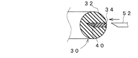
〔Oリング〕
図2に示すように、Oリング30の一部には、回路チップ40が埋めこまれている。Oリング30の本体部32の材質は、フッ素系ゴムなど、弾力性が良好であるとともに、処理室12で発生する高熱や腐食性ガス、プラズマガスなどに対して耐久性のある材料が使用される。回路チップ40は、半導体素子やIC回路などからなり、電気的あるいは電子的な回路機能を果たす微小な部品である。
A workpiece W such as a semiconductor wafer is disposed on the
An O-
[O-ring]
As shown in FIG. 2, a
この実施形態では、回路チップ40として、圧力センサが使用されている。回路チップ40に接続された配線42が、本体部32の外まで引き出されている。回路チップ40の圧力センサで検知された情報が、配線42から外部に伝達される。
図1に示すように、配線42は、半導体装置10の外部に設置された情報処理装置43に接続されている。情報処理装置43は、コンピュータなどからなり、情報処理装置43とOリング30の回路チップ40とが、配線42を介して情報のやり取りを行うことができる。
図3は、Oリング30の詳細な構造を示している。図3(a)に示すように、断面円形の本体部32に対して、外周側から水平方向で直径に沿って、薄板状の回路チップ40が埋めこまれている。回路チップ40の先端は、Oリング30の円形断面において鉛直方向の中心線Cよりも内周側まで到達している。
In this embodiment, a pressure sensor is used as the
As shown in FIG. 1, the
FIG. 3 shows the detailed structure of the O-
〔Oリングの装着状態〕
図4は、Oリング30の装着状態を詳しく示している。半導体製造装置10の処理室12の開口周縁に形成された収容溝13にOリング30が収容される。Oリング30の外周側から引き出された配線42は、処理室12の開口周縁に収容溝13から外周端まで形成された配線溝15に沿って延びて、処理室12の外側まで引き出されている。
処理室12の上面に蓋体14を被せて、蓋体14をボルト締結などで処理室12に締め付け固定すると、装着前は断面円形であったOリング30が、上下に押し潰された扁平な円形状になる。Oリング30が弾力的に変形することによって発生する反発力で、Oリング30と蓋体14の下面との間が圧接されて接触面圧が発生し、封止機能が発現する。Oリング30と収容溝13の底面との間も圧接されて、接触面圧による封止機能が働く。
[O-ring wearing state]
FIG. 4 shows the mounting state of the O-
When the upper surface of the
Oリング30の本体部32に発生する内部圧力あるいは歪みが、回路チップ40の圧力センサで検知される。本体部32に加わる圧力は主に、本体部32と蓋体14の下面との接触領域と、本体部32と収容溝13の底面との接触領域との間に発生するので、この上下の領域間に回路チップ40の圧力センサが存在している必要がある。また、回路チップ40の平面が、Oリング30に加わる圧力の方向、すなわち垂直方向に対して直交するように配置されている。これによって、Oリング30の内部圧力の変化を高感度で正確に検知することができる。
回路チップ40の圧力センサで検知された情報は、配線42を介して情報処理装置43に伝達される。情報処理装置43では、圧力センサの出力情報が、予め設定された許容範囲にあるか否かを判断したり、経時的な変化データを蓄積したり、異常が発生した場合に警報を発したりする。
Internal pressure or distortion generated in the
Information detected by the pressure sensor of the
図4の装着状態では、Oリング30の内周側に、処理室12の内部における真空圧が加わり、処理室12内で発生する処理ガスやプラズマが接触する可能性がある。しかし、Oリング30の内周側には、通常のOリングと同様に本体部32が存在しているだけなので、Oリング30の封止機能には何ら支障は生じない。Oリング30の外周側に露出する回路チップ40の端部や配線42が、腐食性の雰囲気に晒されることもない。配線42を収容した配線溝15が、処理室12の外側の外界と連通していても、封止機能が損なわれることはない。
〔Oリングの内部圧力による性能判定〕
Oリング30の寿命あるいは封止機能の低下を、回路チップ40の圧力センサからの情報によって知ることができる。
In the mounted state of FIG. 4, the vacuum pressure in the
[Performance judgment based on internal pressure of O-ring]
The life of the O-
Oリング30の封止機能は、Oリング30とその両側に存在する部材、例えば、蓋体14および収容溝13の底面との間の接触面圧によって果たされる。十分な接触面圧があれば、ガス等の漏洩は生じない。接触面圧が低下すると、ガスなどが漏洩し易くなり、封止機能が低下したことになる。
通常、Oリング30の使用開始時には、締め付け力によってOリング30の内部に応力が生じ、この内部応力に対応する十分な大きさの接触面圧が発生する。経時とともに、Oリング30の内部で応力緩和が進行して、接触面圧が小さくなり、封止機能が低下する。そして、接触面圧が所定の限界値を下回ると、Oリング30の寿命であると判定できる。但し、使用中のOリング30に対して、封止機能を損なわずに、接触面圧の変化を直接に測定することは困難である。
The sealing function of the O-
Usually, at the start of use of the O-
そこで、Oリング30の内部に発生する応力の変化を検知することで、前記した接触面圧の変化を間接的に知り、Oリング30の性能低下や寿命を予測することができる。
Oリング30の内部応力を検知するには、Oリング30の内部に、圧力センサを組み込んだ回路チップ40を埋め込んでおけばよい。Oリング30に発生する内部応力に対応して、Oリング30の内部に発生し圧力センサで検知される圧力が変化する。圧力センサとして、例えば、ひずみゲージ式の圧力センサを使用すれば、Oリング30の内部に生じている歪み量の変化を捉えて内部応力の変化を検知することができる。
接触面圧に対応するOリング30の歪みは主に、接触面圧が加わる方向に生じる。例えば、図4では、垂直方向に接触面圧が加わり、垂直方向に歪みが生じる。したがって、Oリング30に埋め込まれた回路チップ40の圧力センサで内部応力の変化を知るには、垂直方向の圧力あるいは歪みが検知し易い位置および姿勢で配置しておくことが望ましい。図4では、Oリング30の水平方向に埋め込まれ、Oリング30の垂直方向の中心線Cに配置された回路チップ40の圧力センサが、Oリング30の垂直方向における圧力を検知しており、Oリング30の内部応力を高感度で正確に検知することができる。
Therefore, by detecting a change in the stress generated inside the O-
In order to detect the internal stress of the O-
The distortion of the O-
〔回路チップの取り付け〕
図5は、Oリング30への回路チップ40の取り付け作業を説明する。
Oリング30の本体部32は、通常のOリングと全く同じ材質および形状を有している。市販の標準的なOリング製品がそのまま使用される。
このような本体部32に対して、先端に切刃を有する薄板状の切り込み具50を、本体部32の外周側から水平方向に直径に沿って切り込む。ゴム材料などからなる本体部32は、比較的に容易に切り込むことができる。切り込み具50の先端が所定の位置まで切り込まれたあと、切り込み具50を抜き取る。切り込みの深さを、Oリング30の線径に対して2/3程度に設定することができる。
[Attaching the circuit chip]
FIG. 5 illustrates an operation for attaching the
The
A thin plate-
その後、本体部32に形成された切り込みに、回路チップ40を差し込む。回路チップ40が所定の位置まで差し込まれた状態では、本体部32の切り込みが弾力的に復元することで、回路チップ40を挟み付けて確実に固定される。必要であれば、回路チップ40と本体部32とを接着剤を用いて固定することもできる。回路チップ40の圧力センサを本体部32に一体的に接合させることで、本体部32の内部応力を正確に検知できるようになる。半導体製造装置10のように高熱にさらされる装着個所では、耐熱性接着剤を用いることが望ましい。
〔別の実施形態〕
<挟み込み構造>
図6、7に示す実施形態は、前記実施形態とは回路チップ40の装着構造が異なる。
Thereafter, the
[Another embodiment]
<Pinch structure>
The embodiment shown in FIGS. 6 and 7 differs from the previous embodiment in the mounting structure of the
図6に示すように、微小な矩形片状の回路チップ40を、上下2枚の比較的に大きな正方形の樹脂シート44、44で挟んで接着している。樹脂シート44は、自立状態で水平姿勢を保てる程度の剛性を有している。樹脂シート44の材料として、エポキシ樹脂やイミド樹脂が使用できる。回路チップ40に接続された配線42の一部も樹脂シート44に挟み込まれているが、配線42の端部は樹脂シート44の外側まで延びている。
図7に示すように、樹脂シート44に挟み込まれた状態の回路チップ40を、前記実施形態と同様にして、Oリング30の本体部32に装着する。本体部32に前記同様の切り込みを入れ、切り込みに樹脂シート44、44を差しこむようにすれば、樹脂シート44、44に挟み込まれた回路チップ40は、スムーズに切り込みの奥まで差し込まれる。
As shown in FIG. 6, a small rectangular piece of
As shown in FIG. 7, the
なお、図6のようにして正方形の樹脂シート44、44に回路チップ40を挟み込んだ後、回路チップ40の外側で樹脂シート44の一部を切り取って、必要最小限の大きさにしてから、本体部32の切り込みに差し込むようにしてもよい。
図7では、樹脂シート44、44の一部が、本体部32の外周面から外に少しはみ出しているが、Oリング30の封止機能には問題は生じない。
上記実施形態では、非常に微小な回路チップ40であっても、Oリング30の所定位置に正確かつ容易に装着させることができる。樹脂シート44に挟み込むことによって、回路チップ40の取扱いが行い易くなるとともに、回路チップ40を保護する機能も果たすことができる。
In addition, after sandwiching the
In FIG. 7, a part of the
In the above embodiment, even a very
<突き刺し具>
図8に示す実施形態では、突き刺し具52を用いる。
先が尖った針状の突き刺し具52を、Oリング30の本体部32の外周側から中心に向かって突き刺す。突き刺し具52は、本体部32の内周側に突き抜けないようにしておく。本体部32に生じた穴に、微小な回路チップ40を落とし込むようにして収容する。その後、必要に応じて、本体部32の穴に接着剤34を充填硬化させて埋めてしまえば、回路チップ40は本体部32に埋め込まれた状態になる。接着剤34を、注射針のような細い充填ノズルで穴に注入すれば、周囲を接着剤で汚すことなく、確実に充填することができる。回路チップ40を接着剤とともに充填ノズルで本体部32の穴に注入することもできる。
<Puncture>
In the embodiment shown in FIG. 8, a piercing tool 52 is used.
The needle-like piercing tool 52 having a sharp point is pierced from the outer peripheral side of the
<貼り付け構造>
図9に示す実施形態では、回路チップ40を、Oリング30に貼り付けて取り付ける。
Oリング30の本体部32に対して、接着テープ48を用いて、本体部32の外周側の側面に、回路チップ40を貼り付ける。
回路チップ40には、Oリング30の種別や製造時期、製造番号などの情報を記憶するメモリ回路を設けておけば、Oリング30に管理情報を持たせることができる。回路チップ40には、配線42は備えていないが、誘導電磁波や放射電磁波、赤外線などによって、外部から回路チップ40に電源を供給したり情報を伝達したりする回路を備えておけば、配線42がなくても、外部との情報のやり取りが可能である。具体的には、回路チップ40として、赤外線で情報のやり取りが可能なRFIDチップなどが使用できる。
<Paste structure>
In the embodiment shown in FIG. 9, the
The
If the
Oリング30を半導体製造装置10に装着して使用している状態で、半導体製造装置10の外側に情報処理装置43の読み取り器を近づけて、回路チップ40に記憶された管理情報を読み出すことができる。必要であれば、情報処理装置43から回路チップ40に情報を書き込んだり書き換えたりすることもできる。
上記実施形態では、回路チップ40と接着テープ48とを別々に、あるいは、予め回路チップ40が貼着された接着テープ48の形態で準備しておけば、本体部32のみからなる市販製品などの通常のOリング30を、簡単に回路チップ40付きのOリング30に転換させることができる。Oリング30の使用現場で、必要に応じて、回路チップ40付きのOリング30を作製することができる。
The management information stored in the
In the above-described embodiment, if the
なお、上記実施形態のように、回路チップ40がOリング30の内部に直接に埋め込まれていない形態では、Oリング30の内部応力を検知するのは難しい。
<突き刺しピン>
図10に示す実施形態では、突き刺しピン46を用いる。
押しピン状をなす突き刺しピン46は、先端が鋭く尖っているとともに、ピン軸の途中に突き刺し方向と逆に尖った返り突起を有している。ピン頭部の上に回路チップ40が接合されている。
突き刺しピン46を、Oリング30の本体部32に対して外周側から中心に向かって突き刺すと、突き刺しピン46は本体部32に固定される。突き刺しピン46のピン軸には返り突起を有しているので、Oリング30の使用中に突き刺しピン46が抜け落ちる心配がない。
It should be noted that it is difficult to detect the internal stress of the O-
<Puncture pin>
In the embodiment shown in FIG. 10, a piercing
The piercing
When the piercing
前記した図9の実施形態と同様に、回路チップ40にはOリング30の管理情報が記憶され、配線42なしで外部との情報のやり取りを行う。
回路チップ40が微小であれば、突き刺しピン46のピン軸の内部に埋め込んでおくこともできる。このようにすれば、回路チップ40を本体部32の中心近くまでに配置することが容易である。
上記実施形態では、予め回路チップ40が取り付けられた突き刺しピン46を準備しておけば、本体部32のみからなる市販製品などの通常のOリング30を、簡単に回路チップ40付きのOリング30に転換させることができる。
Similar to the above-described embodiment of FIG. 9, management information of the O-
If the
In the above-described embodiment, if the piercing
本発明の封止リングとして、圧力センサを埋め込んだOリングの具体的な実施例とその性能を評価した結果を説明する。
〔Oリング〕
本体部として、市販のOリング製品〔フッ素ゴム製FKM(D0270、日本バルカー社製)、φ5.33mm×53ID〕を用いた。
回路チップとして、市販の圧力センサ〔共和電業社製PSM小型圧力センサ、ひずみゲージ式〕を用いた。圧力センサは、その面と直交する方向に受けた圧力で生じる歪み量に対応する電気的出力が得られる。
As a sealing ring of the present invention, a specific example of an O-ring in which a pressure sensor is embedded and results of evaluating its performance will be described.
[O-ring]
A commercially available O-ring product (fluoro rubber FKM (D0270, manufactured by Nippon Valqua), φ5.33 mm × 53 ID) was used as the main body.
As a circuit chip, a commercially available pressure sensor [PSM small pressure sensor, strain gauge type manufactured by Kyowa Denki Co., Ltd.] was used. The pressure sensor can obtain an electrical output corresponding to the amount of strain generated by the pressure received in the direction perpendicular to the surface.
図5に示すようにして、本体部に外周側から直径に沿って水平方向に切り込みを形成し、薄い板状の圧力センサを挟み込んで固定した。圧力センサに付属する配線は、本体部の外に引き出して、圧力測定器〔共和電業社製WGA型〕に接続した。
〔透過漏洩試験〕
Oリングを漏洩試験装置に装着して、25%圧縮変形させた状態で、経時的にHeリーク量を測定した。温度条件は100℃に設定した。Heリーク量の測定と同時に、Oリングに埋め込んだ圧力センサで、Oリングの内部に生じる歪みすなわち内部応力を測定した。なお、漏洩試験装置で、Oリングの両側に配置された封止部材の表面粗さは3Sであった。
As shown in FIG. 5, a cut was formed in the main body portion in the horizontal direction along the diameter from the outer peripheral side, and a thin plate-shaped pressure sensor was sandwiched and fixed. The wiring attached to the pressure sensor was pulled out of the main body and connected to a pressure measuring device (WGA type manufactured by Kyowa Denki Co., Ltd.).
(Transmission leakage test)
The amount of He leak was measured over time in a state where the O-ring was attached to a leak test apparatus and 25% compression deformed. The temperature condition was set to 100 ° C. Simultaneously with the measurement of the amount of He leak, the pressure sensor embedded in the O-ring was used to measure the strain generated inside the O-ring, that is, internal stress. In the leak test apparatus, the surface roughness of the sealing members disposed on both sides of the O-ring was 3S.
図11に測定結果を示す。図11は、横軸に内部応力緩和率(%)、縦軸にリーク量をとっている。内部応力緩和率は、下式で算出した。
内部応力緩和率(%)=〔(F0−Ft)/F0〕×100
F0:締め付け時の内部応力測定値
Ft:t時間経過時の内部応力測定値
〔試験結果の評価〕
試験結果によれば、Heリーク量から、封止不良であると判定されたのは、試験開始後約1200時間後であった。この時点で、Heリーク量が急激に増えた。
FIG. 11 shows the measurement results. In FIG. 11, the horizontal stress represents the internal stress relaxation rate (%), and the vertical axis represents the amount of leakage. The internal stress relaxation rate was calculated by the following formula.
Internal stress relaxation rate (%) = [(F 0 −F t ) / F 0 ] × 100
F 0 : Internal stress measurement value during tightening F t : Internal stress measurement value after t time [Evaluation of test results]
According to the test results, it was about 1200 hours after the start of the test that the sealing failure was determined from the amount of He leak. At this point, the amount of He leak increased rapidly.
これに対し、内部応力緩和率も経時的に徐々に増えていく。約1200時間経過時点で、内部応力緩和率90%であった。内部応力緩和率が80%までの段階では、Heリーク量は少なく、十分な封止機能が果たされていることが確認できた。
この結果から、内部応力緩和率が80%を超えた段階で、Oリングの使用限界であると判定して、Oリングの交換を行えば良いことが判る。この段階でOリングの交換を行っておけば、Oリングからシール漏れを起こす心配はない。
Oリングに埋め込まれた圧力センサの検知情報を、装着機器の外部などに設置された圧力測定器に情報伝達して監視しておけば、Oリングの交換時期を確実かつ正確に知ることが可能になることが実証された。
On the other hand, the internal stress relaxation rate gradually increases with time. At about 1200 hours, the internal stress relaxation rate was 90%. When the internal stress relaxation rate was up to 80%, the amount of He leak was small, and it was confirmed that a sufficient sealing function was achieved.
From this result, it can be seen that when the internal stress relaxation rate exceeds 80%, the use limit of the O-ring is determined and the O-ring is replaced. If the O-ring is replaced at this stage, there is no fear of causing seal leakage from the O-ring.
If the detection information of the pressure sensor embedded in the O-ring is transmitted to and monitored by a pressure measuring instrument installed outside the equipment, it is possible to know the replacement timing of the O-ring reliably and accurately. Proved to be.
なお、前記試験では、内部応力緩和率80%を、Oリングの交換時期であると判定したが、Oリングの材質や寸法構造、装着環境などの条件によって、Oリングの交換時期であると判定される内部応力緩和率の値は変更される。実際の使用条件に合わせて、前記同様の試験を行なって、Heリーク量が限界値を超えるときの内部応力緩和率の値を求めれば、Oリングの交換時期を正確に決定することができる。また、Oリングの装着環境において要求される封止機能の信頼性などによって、試験によって求められた内部応力緩和率の限界値に所定の安全率を見込んだ値を、Oリングの交換時期としてもよい。 In the above test, it was determined that the internal stress relaxation rate of 80% was the replacement period of the O-ring, but it was determined that it was the replacement period of the O-ring depending on conditions such as the material, dimensional structure, and mounting environment of the O-ring. The value of the internal stress relaxation rate is changed. If the same test as described above is performed in accordance with the actual use conditions to obtain the value of the internal stress relaxation rate when the amount of He leak exceeds the limit value, the replacement time of the O-ring can be accurately determined. Also, the O-ring replacement time can be determined by taking into account the predetermined safety factor in the limit value of the internal stress relaxation rate obtained by the test due to the reliability of the sealing function required in the O-ring mounting environment. Good.
10 半導体製造装置
12 処理室
13 収容溝
14 蓋体
30 Oリング
32 本体部
40 回路チップ
42 配線
43 情報処理装置
50 切り込み具
DESCRIPTION OF
Claims (8)
環状をなし弾性変形可能な本体部と、
前記本体部に一体的に取り付けられ、封止リングの外部との情報伝達手段を有する回路チップとを備え、
前記回路チップが、前記本体部の内部応力を検知するセンサ部を有し、前記封止リングで封止する両部材と封止リングとの接触面の間で本体部の内部に埋め込まれ、センサ部で検知された状態量を前記封止リングの外部に情報伝達する、
封止リング。 It is a sealing ring that is attached to the facing part between members and seals between both members,
An annularly deformable main body, and
A circuit chip that is integrally attached to the main body and has information transmission means with the outside of the sealing ring ;
The circuit chip has a sensor part for detecting internal stress of the main body part, and is embedded in the main body part between the contact surfaces of both the members sealed by the sealing ring and the sealing ring. Information is transmitted to the outside of the sealing ring.
Sealing ring.
前記センサ部が圧力センサである、
請求項1に記載の封止リング。 The main body is formed of an elastic material selected from the group consisting of rubber, resin and elastomer,
The sensor unit is a pressure sensor;
The sealing ring according to claim 1.
前記本体部の内部に埋め込まれた前記回路チップは、前記封止リングを前記半導体製造装置に装着した状態において前記処理室の内部側の空間に露出しない、
請求項1または2に記載の封止リング。 The facing part between the members to which the sealing ring is attached is the facing part between the members constituting the semiconductor manufacturing apparatus between the inside and the outside of the processing chamber of the semiconductor manufacturing apparatus,
The circuit chip embedded in the main body is not exposed to the space on the inner side of the processing chamber in a state where the sealing ring is mounted on the semiconductor manufacturing apparatus.
The sealing ring according to claim 1 or 2.
前記情報伝達手段が、前記封止リングの外部から前記情報記憶部に管理情報を書き込み可能である、
請求項4に記載の封止リング。 The information storage unit can rewrite management information stored therein,
The information transmission means can write management information to the information storage unit from the outside of the sealing ring .
The sealing ring according to claim 4.
請求項4または5に記載の封止リング。 Management information stored in the information storage unit includes information selected from the group consisting of a manufacturing number, a manufacturing time, a use time, a model number, a material, and a use location of the sealing ring ,
The sealing ring according to claim 4 or 5.
前記情報伝達手段が、前記回路チップと、前記封止リングの外部に配置され無線送受信回路を有する情報処理装置との間で無線により情報伝達する無線情報伝達手段である、
請求項1から6までのいずれかに記載の封止リング。 The circuit chip further includes a wireless transmission / reception circuit,
The information transmission means is wireless information transmission means for wirelessly transmitting information between the circuit chip and an information processing apparatus that is disposed outside the sealing ring and has a wireless transmission / reception circuit .
The sealing ring according to any one of claims 1 to 6 .
前記封止リングが前記部材同士の対面個所に装着された状態で、封止リングの前記回路チップとの間で前記情報伝達手段を介して情報が伝達され、回路チップから入力された情報をもとに情報処理を行い、封止リングの寿命、交換時期、性能低下度、異常発生の有無からなる群から選ばれる情報を含む処理情報を出力する情報処理装置と、
を備える封止リング管理システム。 A sealing ring according to any one of claims 1 to 7 ;
In a state where the sealing ring is mounted on the facing part between the members, information is transmitted to and from the circuit chip of the sealing ring via the information transmitting means, and information input from the circuit chip is also stored. An information processing device that outputs information on processing including information selected from the group consisting of the life of the sealing ring, the replacement time, the degree of performance degradation, and the presence or absence of an abnormality ,
A sealing ring management system comprising:
Priority Applications (3)
| Application Number | Priority Date | Filing Date | Title |
|---|---|---|---|
| JP2003338541A JP4431350B2 (en) | 2003-09-29 | 2003-09-29 | Seal ring and its management system |
| PCT/JP2004/014432 WO2005031195A1 (en) | 2003-09-29 | 2004-09-24 | Sealing ring and its managing system |
| US10/570,109 US7398692B2 (en) | 2003-09-29 | 2004-09-24 | Sealing ring and its managing system |
Applications Claiming Priority (1)
| Application Number | Priority Date | Filing Date | Title |
|---|---|---|---|
| JP2003338541A JP4431350B2 (en) | 2003-09-29 | 2003-09-29 | Seal ring and its management system |
Publications (3)
| Publication Number | Publication Date |
|---|---|
| JP2005106137A JP2005106137A (en) | 2005-04-21 |
| JP2005106137A5 JP2005106137A5 (en) | 2006-10-26 |
| JP4431350B2 true JP4431350B2 (en) | 2010-03-10 |
Family
ID=34386159
Family Applications (1)
| Application Number | Title | Priority Date | Filing Date |
|---|---|---|---|
| JP2003338541A Expired - Lifetime JP4431350B2 (en) | 2003-09-29 | 2003-09-29 | Seal ring and its management system |
Country Status (3)
| Country | Link |
|---|---|
| US (1) | US7398692B2 (en) |
| JP (1) | JP4431350B2 (en) |
| WO (1) | WO2005031195A1 (en) |
Families Citing this family (31)
| Publication number | Priority date | Publication date | Assignee | Title |
|---|---|---|---|---|
| KR100653720B1 (en) * | 2005-10-04 | 2006-12-05 | 삼성전자주식회사 | Thermal processing equipment and driving method thereof |
| US7810816B1 (en) * | 2005-12-13 | 2010-10-12 | Horace P. Halling | Seal |
| US20070241510A1 (en) * | 2006-04-12 | 2007-10-18 | Dileo Anthony | Filter seating monitor |
| US8007568B2 (en) | 2006-04-12 | 2011-08-30 | Millipore Corporation | Filter with memory, communication and pressure sensor |
| US20070243113A1 (en) | 2006-04-12 | 2007-10-18 | Dileo Anthony | Filter with memory, communication and concentration sensor |
| US20070240578A1 (en) * | 2006-04-12 | 2007-10-18 | Dileo Anthony | Filter with memory, communication and temperature sensor |
| US20110094310A1 (en) * | 2006-04-12 | 2011-04-28 | Millipore Corporation | Filter with memory, communication and pressure sensor |
| JP4925178B2 (en) * | 2006-09-25 | 2012-04-25 | 大和製罐株式会社 | Container seal defect inspection method |
| JP4925188B2 (en) * | 2007-02-13 | 2012-04-25 | 大和製罐株式会社 | Inspection method for defective sealing of bag-like containers |
| JP4925189B2 (en) * | 2007-02-13 | 2012-04-25 | 大和製罐株式会社 | Inspection method for defective seal of bag-like container with spout |
| DE502007004386D1 (en) * | 2007-02-27 | 2010-08-26 | Freudenberg Carl Kg | seal |
| US8264347B2 (en) * | 2008-06-24 | 2012-09-11 | Trelleborg Sealing Solutions Us, Inc. | Seal system in situ lifetime measurement |
| US8282013B2 (en) | 2009-01-16 | 2012-10-09 | Parker-Hannifin Corporation | RFID-tagged seal |
| DE102009013003A1 (en) * | 2009-03-13 | 2010-09-16 | Knorr-Bremse Systeme für Nutzfahrzeuge GmbH | Sealing component with electronic component |
| EP2242004B1 (en) * | 2009-04-14 | 2016-01-27 | Carl Freudenberg KG | Component |
| WO2011019888A1 (en) * | 2009-08-13 | 2011-02-17 | Parker-Hannifin Corporation | Sealing assembly with integral sensor |
| DE102011005371A1 (en) | 2011-03-10 | 2012-09-13 | Siemens Aktiengesellschaft | Device for monitoring integrity of screw connection for, e.g. door, has pressure sensor that receives pressure of screw connection components to determine security information and radio interface to transmit security information to reader |
| FR2986615B3 (en) * | 2012-02-07 | 2014-05-23 | Financ De Beaumont Fdb | DEVICE FOR MEASURING AGING CONSTRAINTS OF TECHNICAL PARTS IN / OR INCLUDING ELASTOMER SURFACE MATERIAL |
| US9739402B2 (en) * | 2013-03-04 | 2017-08-22 | Eaton Corporation | Electrically conductive seals for fluid conveyance systems |
| JP6196721B1 (en) * | 2016-10-07 | 2017-09-13 | ジャパンマテックス株式会社 | Gasket for glass lining equipment and manufacturing method thereof |
| RU2677434C1 (en) * | 2018-01-10 | 2019-01-16 | Российская Федерация, от имени которой выступает Государственная корпорация по атомной энергии "Росатом" (Госкорпорация "Росатом") | Sealing device |
| EP3650700B1 (en) * | 2018-11-09 | 2024-02-28 | Pfeiffer Vacuum Gmbh | Vacuum device |
| EP3976999A4 (en) | 2019-05-31 | 2023-06-28 | Greene, Tweed Technologies, Inc. | Smart seals for monitoring and analysis of seal properties useful in semiconductor valves |
| DE112019007862T5 (en) * | 2019-10-30 | 2022-09-01 | Mitsubishi Electric Corporation | VEHICLE MOUNTED DEVICE |
| DE102019131267A1 (en) * | 2019-11-20 | 2021-05-20 | Carl Freudenberg Kg | Sealing arrangement and sealing element |
| RU195568U1 (en) * | 2019-11-28 | 2020-01-31 | Общество с ограниченной ответственностью Управляющая компания "Алтайский завод прецизионных изделий" | FACE SEAL |
| KR20220117313A (en) * | 2019-12-19 | 2022-08-23 | 램 리써치 코포레이션 | RFID encapsulated within a consumable chamber component |
| CN115135916A (en) * | 2020-01-10 | 2022-09-30 | 戈拉特有限公司 | Sealing device and method for producing the same and pipe system |
| DE102020212767A1 (en) | 2020-10-09 | 2022-04-14 | Glatt Gesellschaft Mit Beschränkter Haftung | Sealing device and method for its manufacture and piping system |
| DE102020106470B3 (en) * | 2020-03-10 | 2020-11-26 | Carl Freudenberg Kg | Seal arrangement and its use |
| JP7338571B2 (en) * | 2020-07-02 | 2023-09-05 | トヨタ自動車株式会社 | Deterioration estimation device, deterioration estimation method, deterioration estimation program |
Family Cites Families (8)
| Publication number | Priority date | Publication date | Assignee | Title |
|---|---|---|---|---|
| AU498874B2 (en) * | 1974-09-02 | 1979-03-29 | Rieber + Son A/S | Moulding a pipe end socket |
| US4120521A (en) * | 1975-08-28 | 1978-10-17 | Rieber & Son Plastic-Industri A/S | Combined mould element and sealing ring |
| JP2849894B2 (en) | 1993-11-02 | 1999-01-27 | 株式会社弘電社 | Safety rope with ID tag and safety rope management device |
| JPH09105466A (en) | 1995-10-11 | 1997-04-22 | Mitsubishi Chem Corp | Gland packing seal diagnosing device |
| JP2000304620A (en) | 1999-04-23 | 2000-11-02 | Matsushita Electric Works Ltd | Non-contact id tag |
| JP2002168348A (en) | 2000-11-27 | 2002-06-14 | Seiko Epson Corp | O-ring structure |
| JP2002310333A (en) | 2001-04-17 | 2002-10-23 | Hitachi Ltd | Maintenance timing prediction method for valve and its device |
| JP2003095280A (en) | 2001-09-26 | 2003-04-03 | Toppan Printing Co Ltd | Standing pouch with noncontact type ic chip |
-
2003
- 2003-09-29 JP JP2003338541A patent/JP4431350B2/en not_active Expired - Lifetime
-
2004
- 2004-09-24 WO PCT/JP2004/014432 patent/WO2005031195A1/en active Application Filing
- 2004-09-24 US US10/570,109 patent/US7398692B2/en active Active
Also Published As
| Publication number | Publication date |
|---|---|
| US7398692B2 (en) | 2008-07-15 |
| JP2005106137A (en) | 2005-04-21 |
| US20070012117A1 (en) | 2007-01-18 |
| WO2005031195A1 (en) | 2005-04-07 |
Similar Documents
| Publication | Publication Date | Title |
|---|---|---|
| JP4431350B2 (en) | Seal ring and its management system | |
| KR102081526B1 (en) | Pipe fitting with sensors | |
| JP5101497B2 (en) | Use of a piezoelectric sensor attached to an electronic device package housing | |
| US5693887A (en) | Pressure sensor module having non-contaminating body and isolation member | |
| CA2404468C (en) | Sensor apparatus with two resonant transducers and a single conductor | |
| US20050016303A1 (en) | Sealing device | |
| US9964135B2 (en) | Smart washer for pre-load monitoring | |
| US20150323435A1 (en) | Containment integrity sensor device | |
| JP2008039126A (en) | Monitoring system for valve device | |
| CN112840148A (en) | Smart valve with integrated electronics | |
| CN113167391A (en) | Intelligent valve adaptor with integrated electronics | |
| US11761838B2 (en) | Sensing using nanoparticle based strain sensors | |
| CA2890971A1 (en) | Containment integrity sensor device | |
| US20060025957A1 (en) | Quality assurance system and method | |
| JP2004286551A (en) | Sensor bolt, and bolt inspection system | |
| JP2005148795A (en) | Measuring device and its installation structure | |
| JP2009063171A (en) | Monitoring system of valve apparatus | |
| US11243134B2 (en) | Pressure sensing device isolation cavity seal monitoring | |
| US20050109116A1 (en) | Transducer with integral switch for wireless electronics | |
| JP2006242904A (en) | Suction holder for temperature recording device |
Legal Events
| Date | Code | Title | Description |
|---|---|---|---|
| A521 | Request for written amendment filed |
Free format text: JAPANESE INTERMEDIATE CODE: A523 Effective date: 20060908 |
|
| A621 | Written request for application examination |
Free format text: JAPANESE INTERMEDIATE CODE: A621 Effective date: 20060908 |
|
| TRDD | Decision of grant or rejection written | ||
| A01 | Written decision to grant a patent or to grant a registration (utility model) |
Free format text: JAPANESE INTERMEDIATE CODE: A01 Effective date: 20091208 |
|
| A01 | Written decision to grant a patent or to grant a registration (utility model) |
Free format text: JAPANESE INTERMEDIATE CODE: A01 |
|
| A61 | First payment of annual fees (during grant procedure) |
Free format text: JAPANESE INTERMEDIATE CODE: A61 Effective date: 20091221 |
|
| FPAY | Renewal fee payment (event date is renewal date of database) |
Free format text: PAYMENT UNTIL: 20121225 Year of fee payment: 3 |
|
| R150 | Certificate of patent or registration of utility model |
Ref document number: 4431350 Country of ref document: JP Free format text: JAPANESE INTERMEDIATE CODE: R150 Free format text: JAPANESE INTERMEDIATE CODE: R150 |
|
| FPAY | Renewal fee payment (event date is renewal date of database) |
Free format text: PAYMENT UNTIL: 20131225 Year of fee payment: 4 |
|
| R250 | Receipt of annual fees |
Free format text: JAPANESE INTERMEDIATE CODE: R250 |
|
| R250 | Receipt of annual fees |
Free format text: JAPANESE INTERMEDIATE CODE: R250 |
|
| R250 | Receipt of annual fees |
Free format text: JAPANESE INTERMEDIATE CODE: R250 |
|
| S111 | Request for change of ownership or part of ownership |
Free format text: JAPANESE INTERMEDIATE CODE: R313117 |
|
| R350 | Written notification of registration of transfer |
Free format text: JAPANESE INTERMEDIATE CODE: R350 |
|
| R250 | Receipt of annual fees |
Free format text: JAPANESE INTERMEDIATE CODE: R250 |
|
| R250 | Receipt of annual fees |
Free format text: JAPANESE INTERMEDIATE CODE: R250 |
|
| R250 | Receipt of annual fees |
Free format text: JAPANESE INTERMEDIATE CODE: R250 |
|
| S533 | Written request for registration of change of name |
Free format text: JAPANESE INTERMEDIATE CODE: R313533 |
|
| R350 | Written notification of registration of transfer |
Free format text: JAPANESE INTERMEDIATE CODE: R350 |
|
| R250 | Receipt of annual fees |
Free format text: JAPANESE INTERMEDIATE CODE: R250 |
|
| R250 | Receipt of annual fees |
Free format text: JAPANESE INTERMEDIATE CODE: R250 |
|
| R250 | Receipt of annual fees |
Free format text: JAPANESE INTERMEDIATE CODE: R250 |
|
| R250 | Receipt of annual fees |
Free format text: JAPANESE INTERMEDIATE CODE: R250 |
|
| EXPY | Cancellation because of completion of term |