JP4403387B2 - Solid-state imaging device and driving method of solid-state imaging device - Google Patents
Solid-state imaging device and driving method of solid-state imaging device Download PDFInfo
- Publication number
- JP4403387B2 JP4403387B2 JP2004129388A JP2004129388A JP4403387B2 JP 4403387 B2 JP4403387 B2 JP 4403387B2 JP 2004129388 A JP2004129388 A JP 2004129388A JP 2004129388 A JP2004129388 A JP 2004129388A JP 4403387 B2 JP4403387 B2 JP 4403387B2
- Authority
- JP
- Japan
- Prior art keywords
- potential
- pixel
- reset
- signal line
- imaging device
- Prior art date
- Legal status (The legal status is an assumption and is not a legal conclusion. Google has not performed a legal analysis and makes no representation as to the accuracy of the status listed.)
- Active
Links
- 238000003384 imaging method Methods 0.000 title claims description 24
- 238000000034 method Methods 0.000 title claims description 11
- 239000011159 matrix material Substances 0.000 claims description 8
- 238000006243 chemical reaction Methods 0.000 claims description 7
- 238000012545 processing Methods 0.000 description 37
- 238000009792 diffusion process Methods 0.000 description 36
- 238000012546 transfer Methods 0.000 description 30
- 230000003321 amplification Effects 0.000 description 20
- 238000003199 nucleic acid amplification method Methods 0.000 description 20
- 238000010586 diagram Methods 0.000 description 7
- 230000008859 change Effects 0.000 description 4
- 230000008878 coupling Effects 0.000 description 4
- 238000010168 coupling process Methods 0.000 description 4
- 238000005859 coupling reaction Methods 0.000 description 4
- 230000002411 adverse Effects 0.000 description 3
- 230000000694 effects Effects 0.000 description 3
- 230000002093 peripheral effect Effects 0.000 description 3
- 230000008569 process Effects 0.000 description 3
- 230000003139 buffering effect Effects 0.000 description 2
- 230000004048 modification Effects 0.000 description 2
- 238000012986 modification Methods 0.000 description 2
- 239000000758 substrate Substances 0.000 description 2
- 230000009471 action Effects 0.000 description 1
- 238000004458 analytical method Methods 0.000 description 1
- 238000012937 correction Methods 0.000 description 1
- 230000006866 deterioration Effects 0.000 description 1
- 238000007562 laser obscuration time method Methods 0.000 description 1
- 230000007246 mechanism Effects 0.000 description 1
- 230000010355 oscillation Effects 0.000 description 1
- 238000012827 research and development Methods 0.000 description 1
- 238000005070 sampling Methods 0.000 description 1
- 239000004065 semiconductor Substances 0.000 description 1
- 230000007704 transition Effects 0.000 description 1
Images


Classifications
-
- H—ELECTRICITY
- H01—ELECTRIC ELEMENTS
- H01L—SEMICONDUCTOR DEVICES NOT COVERED BY CLASS H10
- H01L27/00—Devices consisting of a plurality of semiconductor or other solid-state components formed in or on a common substrate
- H01L27/14—Devices consisting of a plurality of semiconductor or other solid-state components formed in or on a common substrate including semiconductor components sensitive to infrared radiation, light, electromagnetic radiation of shorter wavelength or corpuscular radiation and specially adapted either for the conversion of the energy of such radiation into electrical energy or for the control of electrical energy by such radiation
- H01L27/144—Devices controlled by radiation
- H01L27/146—Imager structures
- H01L27/14601—Structural or functional details thereof
- H01L27/14609—Pixel-elements with integrated switching, control, storage or amplification elements
- H01L27/14612—Pixel-elements with integrated switching, control, storage or amplification elements involving a transistor
-
- H—ELECTRICITY
- H01—ELECTRIC ELEMENTS
- H01L—SEMICONDUCTOR DEVICES NOT COVERED BY CLASS H10
- H01L27/00—Devices consisting of a plurality of semiconductor or other solid-state components formed in or on a common substrate
- H01L27/14—Devices consisting of a plurality of semiconductor or other solid-state components formed in or on a common substrate including semiconductor components sensitive to infrared radiation, light, electromagnetic radiation of shorter wavelength or corpuscular radiation and specially adapted either for the conversion of the energy of such radiation into electrical energy or for the control of electrical energy by such radiation
- H01L27/144—Devices controlled by radiation
- H01L27/146—Imager structures
- H01L27/14643—Photodiode arrays; MOS imagers
-
- H—ELECTRICITY
- H04—ELECTRIC COMMUNICATION TECHNIQUE
- H04N—PICTORIAL COMMUNICATION, e.g. TELEVISION
- H04N25/00—Circuitry of solid-state image sensors [SSIS]; Control thereof
- H04N25/60—Noise processing, e.g. detecting, correcting, reducing or removing noise
-
- H—ELECTRICITY
- H04—ELECTRIC COMMUNICATION TECHNIQUE
- H04N—PICTORIAL COMMUNICATION, e.g. TELEVISION
- H04N25/00—Circuitry of solid-state image sensors [SSIS]; Control thereof
- H04N25/60—Noise processing, e.g. detecting, correcting, reducing or removing noise
- H04N25/65—Noise processing, e.g. detecting, correcting, reducing or removing noise applied to reset noise, e.g. KTC noise related to CMOS structures by techniques other than CDS
-
- H—ELECTRICITY
- H04—ELECTRIC COMMUNICATION TECHNIQUE
- H04N—PICTORIAL COMMUNICATION, e.g. TELEVISION
- H04N25/00—Circuitry of solid-state image sensors [SSIS]; Control thereof
- H04N25/60—Noise processing, e.g. detecting, correcting, reducing or removing noise
- H04N25/67—Noise processing, e.g. detecting, correcting, reducing or removing noise applied to fixed-pattern noise, e.g. non-uniformity of response
- H04N25/671—Noise processing, e.g. detecting, correcting, reducing or removing noise applied to fixed-pattern noise, e.g. non-uniformity of response for non-uniformity detection or correction
- H04N25/677—Noise processing, e.g. detecting, correcting, reducing or removing noise applied to fixed-pattern noise, e.g. non-uniformity of response for non-uniformity detection or correction for reducing the column or line fixed pattern noise
-
- H—ELECTRICITY
- H04—ELECTRIC COMMUNICATION TECHNIQUE
- H04N—PICTORIAL COMMUNICATION, e.g. TELEVISION
- H04N25/00—Circuitry of solid-state image sensors [SSIS]; Control thereof
- H04N25/70—SSIS architectures; Circuits associated therewith
- H04N25/71—Charge-coupled device [CCD] sensors; Charge-transfer registers specially adapted for CCD sensors
- H04N25/75—Circuitry for providing, modifying or processing image signals from the pixel array
-
- H—ELECTRICITY
- H04—ELECTRIC COMMUNICATION TECHNIQUE
- H04N—PICTORIAL COMMUNICATION, e.g. TELEVISION
- H04N25/00—Circuitry of solid-state image sensors [SSIS]; Control thereof
- H04N25/70—SSIS architectures; Circuits associated therewith
- H04N25/76—Addressed sensors, e.g. MOS or CMOS sensors
- H04N25/766—Addressed sensors, e.g. MOS or CMOS sensors comprising control or output lines used for a plurality of functions, e.g. for pixel output, driving, reset or power
-
- H—ELECTRICITY
- H04—ELECTRIC COMMUNICATION TECHNIQUE
- H04N—PICTORIAL COMMUNICATION, e.g. TELEVISION
- H04N25/00—Circuitry of solid-state image sensors [SSIS]; Control thereof
- H04N25/70—SSIS architectures; Circuits associated therewith
- H04N25/76—Addressed sensors, e.g. MOS or CMOS sensors
- H04N25/767—Horizontal readout lines, multiplexers or registers
-
- H—ELECTRICITY
- H04—ELECTRIC COMMUNICATION TECHNIQUE
- H04N—PICTORIAL COMMUNICATION, e.g. TELEVISION
- H04N25/00—Circuitry of solid-state image sensors [SSIS]; Control thereof
- H04N25/70—SSIS architectures; Circuits associated therewith
- H04N25/76—Addressed sensors, e.g. MOS or CMOS sensors
- H04N25/77—Pixel circuitry, e.g. memories, A/D converters, pixel amplifiers, shared circuits or shared components
- H04N25/772—Pixel circuitry, e.g. memories, A/D converters, pixel amplifiers, shared circuits or shared components comprising A/D, V/T, V/F, I/T or I/F converters
-
- H—ELECTRICITY
- H04—ELECTRIC COMMUNICATION TECHNIQUE
- H04N—PICTORIAL COMMUNICATION, e.g. TELEVISION
- H04N25/00—Circuitry of solid-state image sensors [SSIS]; Control thereof
- H04N25/70—SSIS architectures; Circuits associated therewith
- H04N25/76—Addressed sensors, e.g. MOS or CMOS sensors
- H04N25/77—Pixel circuitry, e.g. memories, A/D converters, pixel amplifiers, shared circuits or shared components
- H04N25/778—Pixel circuitry, e.g. memories, A/D converters, pixel amplifiers, shared circuits or shared components comprising amplifiers shared between a plurality of pixels, i.e. at least one part of the amplifier must be on the sensor array itself
Description
本発明は、固体撮像装置および固体撮像装置の駆動方法に関し、特にCMOS型(あるいは、MOS型)の固体撮像装置および当該固体撮像装置の駆動方法に関する。 The present invention relates to a solid-state imaging device and a driving method of the solid-state imaging device, and more particularly to a CMOS type (or MOS type) solid-state imaging device and a driving method of the solid-state imaging device.
固体撮像装置として、CMOS集積回路と同様のプロセスで製造できるCMOS型固体撮像装置(以下、CMOSイメージセンサと記す)が知られている(例えば、特許文献1参照)。CMOSイメージセンサは、CMOSプロセスに付随した微細化技術により、画素毎に増幅機能を持つアクティブ型の構造が容易に作ることができ、また画素アレイ部を駆動する駆動回路や当該画素アレイ部の各画素から出力される信号を処理する信号処理回路などの周辺回路部を、画素アレイ部と同一チップ(基板)上に集積できるという特長を持っている。このため、近年、CMOSイメージセンサが注目され、当該CMOSイメージセンサに関してより多くの研究・開発がなされている。 As a solid-state imaging device, a CMOS type solid-state imaging device (hereinafter referred to as a CMOS image sensor) that can be manufactured by a process similar to that of a CMOS integrated circuit is known (for example, see Patent Document 1). In the CMOS image sensor, an active structure having an amplification function for each pixel can be easily made by a miniaturization technique associated with the CMOS process, and a driving circuit for driving the pixel array unit and each pixel array unit are provided. A peripheral circuit unit such as a signal processing circuit that processes a signal output from a pixel can be integrated on the same chip (substrate) as the pixel array unit. For this reason, in recent years, CMOS image sensors have attracted attention, and more research and development have been conducted on the CMOS image sensors.
本発明者の解析により、CMOSイメージセンサ等の固体撮像装置において、その画質劣化の原因の一つが、次のような機構に起因することがわかった。すなわち、画素から信号が垂直信号線に出力されると、当該垂直信号線の電位が変化する。このとき、画素から信号を1行毎に読み出していても、垂直信号線の電位は画素アレイ部の全面に亘って変化する。このため、画素アレイ部のウェルの電位が、画素アレイ部の全面に亘る容量結合によって振られて揺れてしまう。画素からの信号の読み出し中に、画素アレイ部のウェルの電位が揺れると、その電位の揺れが画素の信号に乗り、ノイズやシェーディング(撮像画面上の大域的なむら)を引き起こす要因となる。 According to the analysis of the present inventor, it has been found that one of the causes of image quality deterioration in a solid-state imaging device such as a CMOS image sensor is due to the following mechanism. That is, when a signal is output from the pixel to the vertical signal line, the potential of the vertical signal line changes. At this time, even when signals are read from the pixels for each row, the potential of the vertical signal line changes over the entire surface of the pixel array portion. For this reason, the potential of the well of the pixel array unit is shaken by being shaken by capacitive coupling over the entire surface of the pixel array unit. If the potential of the well of the pixel array portion fluctuates during reading of a signal from the pixel, the fluctuation of the potential rides on the pixel signal and causes noise and shading (global unevenness on the imaging screen).
本発明は、上記課題に鑑みてなされたものであって、その目的とするところは、画素からの信号の読み出し中に、画素アレイ部のウェル電位の揺れを抑えることで、当該電位の揺れに起因するノイズやシェーディングの発生を防止することを可能とした固体撮像装置および固体撮像装置の駆動方法を提供することにある。 The present invention has been made in view of the above problems, and the object of the present invention is to suppress the fluctuation of the well potential of the pixel array portion during reading of the signal from the pixel, thereby suppressing the fluctuation of the potential. An object of the present invention is to provide a solid-state imaging device and a driving method for the solid-state imaging device that can prevent the occurrence of noise and shading caused by the noise.
上記目的を達成するために、本発明では、
光電変換素子を含む画素が行列状に2次元配置され、当該行列状配置の列ごとに信号線が配線されてなる画素アレイ部と、
前記画素アレイ部の各画素を行単位で走査するとともに、該当行の画素を駆動する垂直駆動回路と
を備える固体撮像装置において、
前記垂直駆動回路による駆動の下に、ある行の画素が動作を終了し、次の行の画素が動作期間に入る前に、前記信号線の電位を第1の電源電位と第2の電源電位との中間電位に固定する
ことを特徴としている。
In order to achieve the above object, in the present invention,
A pixel array unit in which pixels including photoelectric conversion elements are two-dimensionally arranged in a matrix and signal lines are wired for each column in the matrix ;
A vertical driving circuit that scans each pixel of the pixel array unit in units of rows and drives pixels in the corresponding row;
In a solid-state imaging device comprising:
Under the driving by the vertical drive circuit, the pixels of a certain row finish the operation, and before the pixels of the next row enter the operation period, the potential of the signal line is set to the first power supply potential and the second power supply potential. It is characterized by being fixed at an intermediate potential.
上記構成の固体撮像装置において、画素が動作期間に入る前に、信号線の電位を中間電位に固定すると、画素から信号線にリセットレベルを出力する際に、信号線の電位が中間電位からリセットレベルに遷移することになるためその変化幅は小さい。これにより、リセットレベルの出力時における信号線の電位揺れ(変化)を最小限に抑えられるため、信号線の電位揺れに伴う画素アレイ部のウェル電位の揺れが抑えられる。 In the solid-state imaging device having the above configuration, when the signal line potential is fixed to the intermediate potential before the pixel enters the operation period, the signal line potential is reset from the intermediate potential when the reset level is output from the pixel to the signal line. Since the level transitions, the change width is small. Thereby, since the potential fluctuation (change) of the signal line at the output of the reset level can be minimized, the fluctuation of the well potential of the pixel array portion due to the potential fluctuation of the signal line can be suppressed.
本発明によれば、信号線の電位揺れに伴う画素アレイ部のウェル電位の揺れを抑え、リセットレベルと信号レベルに悪影響を及ぼすのを確実に防ぐことができるため、当該ウェル電位の揺れに起因するノイズやシェーディングの発生を防止することができる。 According to the present invention, it is possible to suppress the fluctuation of the well potential of the pixel array unit due to the fluctuation of the potential of the signal line and to surely prevent the reset level and the signal level from being adversely affected. Noise and shading can be prevented.
以下、本発明の実施の形態について図面を参照して詳細に説明する。 Hereinafter, embodiments of the present invention will be described in detail with reference to the drawings.
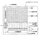
図1は、本発明が適用される固体撮像装置、例えばCMOSイメージセンサの全体の構成を示すブロック図である。なお、ここでは、CMOS型の固体撮像装置に適用する場合を例に挙げて説明するが、本発明はこの適用例に限られるものではなく、MOS型の固体撮像装置にも同様に適用可能である。 FIG. 1 is a block diagram showing the overall configuration of a solid-state imaging device to which the present invention is applied, for example, a CMOS image sensor. Here, the case where the present invention is applied to a CMOS type solid-state imaging device will be described as an example. However, the present invention is not limited to this application example, and can be similarly applied to a MOS type solid-state imaging device. is there.
図1に示すように、本適用例に係るCMOSイメージセンサ10は、光電変換素子を含む画素11が行列状(マトリックス状)に多数2次元配置されてなる画素アレイ部12に加えて、垂直(V)駆動回路13、カラム処理部14、水平(H)駆動回路15、水平信号線16、出力回路17およびタイミング制御回路18を有する構成となっている。
As shown in FIG. 1, the CMOS image sensor 10 according to this application example includes a vertical (in addition to a pixel array unit 12 in which a large number of pixels 11 including photoelectric conversion elements are two-dimensionally arranged in a matrix (matrix). V) The
このシステム構成において、タイミング制御回路18は、垂直同期信号Vsync、水平同期信号HsyncおよびマスタークロックMCKに基づいて、垂直駆動回路13、カラム処理部14および水平駆動回路15などの動作の基準となるクロック信号や制御信号などを生成し、垂直駆動回路13、カラム処理部14および水平駆動回路15などに対して与える。また、画素アレイ部12の各画素11を駆動制御する周辺の駆動回路や信号処理回路部、即ち垂直駆動回路13、カラム処理部14、水平駆動回路15、水平信号線16、出力回路17およびタイミング制御回路18などは、画素アレイ部12と同一の半導体基板(チップ)19上に集積される。
In this system configuration, the
画素アレイ部12には、画素11がm行n列分(ここでは、図面の簡略化のため10行12列分の画素配列を示している)だけ2次元配置されるとともに、このm行n列の画素配置に対して行ごとに行制御線(図示せず)が配線され、列ごとに垂直信号線121(121−1〜121−n)が配線されている。垂直駆動回路13は、シフトレジスタなどによって構成され、画素アレイ部12の各画素11を行単位で順次選択し、その選択行の各画素に対して上記行選択線を通して必要なパルスを供給する。
In the pixel array unit 12, pixels 11 are two-dimensionally arranged for m rows and n columns (here, a pixel array for 10 rows and 12 columns is shown for simplification of the drawing), and this m rows and n columns are arranged. A row control line (not shown) is wired for each row in the column pixel arrangement, and vertical signal lines 121 (121-1 to 121-n) are wired for each column. The
選択行の各画素から出力される信号は、垂直信号線121を通してカラム処理部14に供給される。カラム処理部14には、画素アレイ部12の各画素列に対応してカラム信号処理回路141が設けられている。カラム信号処理回路141は、1行分の画素11から出力される信号を画素列ごとに受けて、その信号に対して画素11固有の固定パターンノイズを除去するためのCDS(Correlated Double Sampling;相関二重サンプリング)や信号増幅あるいは必要に応じてA/D(アナログ/デジタル)変換などの処理を行う。 A signal output from each pixel in the selected row is supplied to the column processing unit 14 through the vertical signal line 121. The column processing unit 14 is provided with a column signal processing circuit 141 corresponding to each pixel column of the pixel array unit 12. The column signal processing circuit 141 receives signals output from the pixels 11 for one row for each pixel column, and removes fixed pattern noise specific to the pixels 11 from the signals. (Double sampling), signal amplification, or A / D (analog / digital) conversion, if necessary.
水平駆動回路15は、シフトレジスタなどによって構成され、カラム処理部14のカラム信号処理回路141の各々を順番に選択し、カラム信号処理回路141の各々から出力される信号を水平信号線16に導く。出力回路17は、カラム信号処理回路141の各々から水平信号線16を通して順に供給される信号に対して種々の信号処理を施して出力する。この出力回路17での具体的な信号処理としては、例えば、バッファリングだけする場合もあるし、あるいはバッファリングの前に黒レベル調整、列ごとのばらつきの補正、信号増幅、色関係処理などを行うこともある。
The
(実施例1)
図2は、本発明の実施例1に係るCMOSイメージセンサの要部の構成、即ち画素およびカラム信号処理回路の一部の構成を示す回路図である。ここでは、ある1つの画素11Aと、当該画素11Aの列の垂直信号線121に繋がるカラム信号処理回路141の一部の回路構成のみを示している。
Example 1
FIG. 2 is a circuit diagram showing a configuration of a main part of the CMOS image sensor according to the first embodiment of the present invention, that is, a configuration of a part of the pixel and column signal processing circuit. Here, only a part of the circuit configuration of the column signal processing circuit 141 connected to one pixel 11A and the vertical signal line 121 of the column of the pixel 11A is shown.
図2において、画素11Aは、光電変換素子、例えばフォトダイオード(PD)21に加えて、転送トランジスタ22、リセットトランジスタ23、増幅トランジスタ24および選択トランジスタ25の4つのトランジスタを有する構成となっている。ここでは、転送トランジスタ22、リセットトランジスタ23、増幅トランジスタ24および選択トランジスタ25として、NchMOSトランジスタを用いた例を示しているが、PchMOSトランジスタを用いることも可能である。
In FIG. 2, the pixel 11 </ b> A includes four transistors, that is, a
フォトダイオード21は、アノードが第1の電源電位、例えばグランドに接続されており、入射光をその光量に応じた電荷量の信号電荷(光電子)に光電変換し、当該信号電荷を蓄積する。転送トランジスタ22は、ドレインがフローティングディフュージョンFDに、ソースがフォトダイオード21のカソードに、ゲートが転送配線26にそれぞれ接続されており、垂直駆動回路13から転送パルスTRFが転送配線26を通してゲートに与えられるとオン(導通)状態となって、フォトダイオード21に蓄積されている信号電荷をフローティングディフュージョンFDに転送する。
The photodiode 21 has an anode connected to a first power supply potential, for example, the ground, photoelectrically converts incident light into a signal charge (photoelectron) having a charge amount corresponding to the light amount, and accumulates the signal charge. In the
リセットトランジスタ23は、ドレインが第2の電源電位、例えば電源電位VDD(例えば、2.5V)の電源配線27に、ソースがフローティングディフュージョンFDに、ゲートがリセット配線28にそれぞれ接続されており、垂直駆動回路13からリセットパルスRSTがリセット配線28を通してゲートに与えられるとオン状態となり、フローティングディフュージョンFDの信号電荷を電源配線27に捨てることによって当該フローティングディフュージョンFDをリセットする。
The
増幅トランジスタ24は、ドレインが電源配線27に、ゲートがフローティングディフュージョンFDにそれぞれ接続されており、当該フローティングディフュージョンFDの電位に対応した信号を出力する。選択トランジスタ25は、ドレインが増幅トランジスタ24のソースに、ソースが垂直信号線121に、ゲートが選択配線29にそれぞれ接続されており、垂直駆動回路13から選択パルスSELが選択配線29を通してゲートに与えられるとオン状態となって当該画素11Aを選択し、増幅トランジスタ24から出力される画素11Aの信号を垂直信号線121に読み出す。
The
転送配線26、リセット配線28および選択配線29は、同一行の画素11Aについて共通に配線されている。そして、これら転送配線26、リセット配線28および選択配線29には、上述したように、転送パルスTRF、リセットパルスRSTおよび選択パルスSELが垂直駆動回路13から適宜与えられることで、フォトダイオード21からフローティングディフュージョンFDへの信号電荷の転送動作、フローティングディフュージョンFDのリセット動作および画素11Aの選択動作の制御が行われる。
The transfer wiring 26, the reset wiring 28, and the selection wiring 29 are wired in common for the pixels 11A in the same row. Then, as described above, the transfer pulse TRF, the reset pulse RST, and the selection pulse SEL are appropriately supplied from the
カラム信号処理回路141の入力段には、例えばNchのMOSトランジスタが負荷トランジスタ31として設けられている。この負荷(MOS)トランジスタ31は、ドレインが垂直信号線121に、ソースがグランドにそれぞれ接続され、画素11Aの増幅トランジスタ24と共に、垂直信号線121を介してソースフォロアを形成することで定電流源をなしており、ゲートにロードパルスLOADが与えられることによってオン状態となり、画素11Aの信号を増幅トランジスタ24を通して垂直信号線121に出力させる。
For example, an Nch MOS transistor is provided as a
カラム信号処理回路141にはさらに、画素11Aが動作期間に入る前の垂直信号線121の電位を、電源配線27の電位VDDとグランド電位との中間電位Vmidに固定する手段として例えばPchのMOSトランジスタ(以下、固定トランジスタと記す)32が設けられている。固定トランジスタ32は、ソースが垂直信号線121に、ドレインが所定の中間電位Vmidにそれぞれ接続されており、ゲートに“L”レベルの固定パルスFIXが与えられることでオン状態となり、垂直信号線121に中間電位Vmidを与えることで、垂直信号線121の電位を中間電位Vmidに固定する。ここでは、中間電位Vmidとして、電源電位VDD=2.5Vに対して例えば1.5Vを設定する。
The column signal processing circuit 141 further includes, for example, a Pch MOS transistor as means for fixing the potential of the vertical signal line 121 before the pixel 11A enters the operation period to an intermediate potential Vmid between the potential VDD of the power supply wiring 27 and the ground potential. 32 (hereinafter referred to as a fixed transistor) is provided. The fixed
図3は、上記構成の実施例1に係るCMOSイメージセンサの駆動タイミングを示すタイミングチャートである。ここでは、ロードパルスLOAD、固定パルスFIX、選択パルスSEL、リセットパルスRSTおよび転送パルスTRFに加え、垂直信号線121の電位の概略の波形をも示し、説明のため縦軸スケールを異ならせている。ここで、固定パルスFIXについては“L”レベルの状態がアクティブ状態となり、それ以外のロードパルスLOAD、選択パルスSEL、リセットパルスRSTおよび転送パルスTRFについては“H”レベルの状態がアクティブ状態となる。また、ロードパルスLOADの“H”レベルについては、負荷トランジスタ31が定電流源となる電圧(約1V)である。
FIG. 3 is a timing chart showing the drive timing of the CMOS image sensor according to the first embodiment having the above-described configuration. Here, in addition to the load pulse LOAD, the fixed pulse FIX, the selection pulse SEL, the reset pulse RST, and the transfer pulse TRF, a schematic waveform of the potential of the vertical signal line 121 is also shown, and the vertical axis scale is varied for explanation. . Here, for the fixed pulse FIX, the “L” level state becomes the active state, and for the other load pulses LOAD, selection pulse SEL, reset pulse RST and transfer pulse TRF, the “H” level state becomes the active state. . The “H” level of the load pulse LOAD is a voltage (about 1 V) at which the
画素11Aの動作前では、固定パルスFIXがアクティブの状態にあり、よって固定トランジスタ32がオン状態となって中間電位Vmidを垂直信号線121に与える。これにより、画素11Aの動作前には、垂直信号線121の電位が電源配線27の電位VDDとグランド電位との中間電位Vmid(ここでは、1.5V)に固定された状態にある。この固定状態から固定パルスFIXが非アクティブの状態に移行しても、短時間の間は垂直信号線121の電位が中間電位Vmid付近に保たれる。
Before the operation of the pixel 11A, the fixed pulse FIX is in an active state, so that the fixed
その後、ロードパルスLOADおよび選択パルスSELがアクティブになると同時に、リセットパルスRSTが入ることで、画素11AのフローティングディフュージョンFDがリセットトランジスタ23によってリセットされ、このリセット後のフローティングディフュージョンFDの電位がリセットレベルとしてリセットレベルとして増幅トランジスタ24によって垂直信号線121に出力される。
Thereafter, the load pulse LOAD and the selection pulse SEL become active, and at the same time, the reset pulse RST is input, so that the floating diffusion FD of the pixel 11A is reset by the
このリセットレベルの出力後、転送パルスTRFが入ることで、フォトダイオード21の信号電荷(光電子)が転送トランジスタ22によってフローティングディフュージョンFDに転送され、この転送後のフローティングディフュージョンFDの電位が信号レベルとして増幅トランジスタ24によって垂直信号線121に出力される。これらリセットレベルおよび信号レベルは順次、垂直信号線121を通してカラム信号処理回路141へ送られる。
When the transfer pulse TRF is input after the reset level is output, the signal charge (photoelectron) of the photodiode 21 is transferred to the floating diffusion FD by the
カラム信号処理回路141では、例えば、リセットレベルと信号レベルとの差をとることで画素11A固有の固定パターンノイズを除去するCDS処理、CDS処理後の信号の保持、あるいは増幅などの種々の信号処理が行われる。 In the column signal processing circuit 141, for example, various signal processing such as CDS processing for removing the fixed pattern noise inherent to the pixel 11A by taking the difference between the reset level and the signal level, holding the signal after CDS processing, or amplification. Is done.
その後、ロードパルスLOADおよび選択パルスSELが非アクティブ状態になり、しかる後固定パルスFIXがアクティブ状態になると、固定トランジスタ32がオン状態となって中間電位Vmidを垂直信号線121に与えるため、垂直信号線121の電位が再び中間電位Vmidに固定される。この後に、カラム信号処理回路141から信号が出力される期間(有効期間)となる。
After that, when the load pulse LOAD and the selection pulse SEL become inactive, and then the fixed pulse FIX becomes active, the fixed
ここで、画素11Aから垂直信号線121に信号が出力され、垂直信号線121の電位が変化するときに、容量結合(カップリング)によって画素アレイ部12のウェル電位が揺らされる。画素11Aからリセットレベルや信号レベルが出力されている期間に画素アレイ部12のウェル電位が揺れていると、先述したように、当該ウェル電位の揺れがリセットレベルと信号レベルに影響を及ぼすため、ノイズやシェーディングの原因となる。そこで、本実施例1に係るCMOSイメージセンサでは、固定トランジスタ32の作用により、画素11Aの動作期間に入る直前に垂直信号線121の電位を中間電位Vmidに固定し、画素アレイ部12のウェルの電位が揺らされないようにしている。
Here, when a signal is output from the pixel 11A to the vertical signal line 121 and the potential of the vertical signal line 121 changes, the well potential of the pixel array unit 12 is fluctuated by capacitive coupling. If the well potential of the pixel array unit 12 fluctuates during the period when the reset level and the signal level are output from the pixel 11A, as described above, the fluctuation of the well potential affects the reset level and the signal level. Causes noise and shading. Therefore, in the CMOS image sensor according to the first embodiment, the potential of the vertical signal line 121 is fixed to the intermediate potential Vmid immediately before the operation period of the pixel 11A is entered by the action of the fixed
このとき一番大きなのが、画素11Aが動作を始める前に、垂直信号線121の電位が何ボルトになっているかである。垂直信号線121の電位が例えば0VやVDDレベルにあり、これらのレベルからリセットレベルに急激に遷移すると、垂直信号線121の電位が大きく変化し、これに伴って画素アレイ部12のウェル電位が揺れることになるため、当該ウェル電位の揺れがリセットレベルと信号レベルに影響を及ぼし、ノイズやシェーディングが発生する。 At this time, the biggest thing is how many volts the potential of the vertical signal line 121 is before the pixel 11A starts its operation. When the potential of the vertical signal line 121 is at, for example, 0V or VDD level, and when the level rapidly changes from these levels to the reset level, the potential of the vertical signal line 121 changes greatly, and accordingly, the well potential of the pixel array unit 12 changes. Since the oscillation of the well potential affects the reset level and the signal level, noise and shading occur.
従来のCMOSイメージセンサでは、画素11Aが動作を始める前の垂直信号線121の電位は、0Vまたは電源電位VDDになっているか、またはフローティング状態にあった。フローティング状態の場合には、フォトダイオード21を外れて垂直信号線121の拡散層に流入する光電子によって、光量が大きいときには0V近辺まで電位が下がってしまうことから、やはり好ましくない。 In the conventional CMOS image sensor, the potential of the vertical signal line 121 before the operation of the pixel 11A is 0 V, the power supply potential VDD, or is in a floating state. In the floating state, the potential drops to around 0 V when the amount of light is large due to the photoelectrons flowing out of the photodiode 21 and flowing into the diffusion layer of the vertical signal line 121, which is not preferable.
そこで、本実施例1に係るCMOSイメージセンサにおいては、画素11Aが動作期間に入る前の垂直信号線121の電位を、電源電位VDDとグランド電位(0V)との中間電位Vmid、具体的には電源電電位VDD=2.5Vに対して例えば1.5Vの電位に固定することで、リセットレベルに遷移するときの垂直信号線121の電位揺れ(変化)を最小限に抑えるようにしている。これにより、垂直信号線121の電位揺れに伴う画素アレイ部12のウェル電位の揺れが、リセットレベルと信号レベルに悪影響を及ぼすのを最小限にすることができるため、当該ウェル電位の揺れに起因するノイズやシェーディングの発生を最小限にすることができる。 Therefore, in the CMOS image sensor according to the first embodiment, the potential of the vertical signal line 121 before the pixel 11A enters the operation period is set to the intermediate potential Vmid between the power supply potential VDD and the ground potential (0V), specifically, By fixing the power supply potential VDD = 2.5V to, for example, a potential of 1.5V, the potential fluctuation (change) of the vertical signal line 121 when transitioning to the reset level is minimized. As a result, the fluctuation of the well potential of the pixel array unit 12 due to the fluctuation of the potential of the vertical signal line 121 can minimize the adverse effect on the reset level and the signal level. Noise and shading can be minimized.
垂直信号線121の電位の揺れを最小限に抑えるには、中間電位Vmidをリセットレベル付近に設定するのが好ましい。リセットトランジスタ23とフローティングディフュージョンFDのカップリングによって、垂直信号線121の電位が例えば0.3V程度変化する。この例では、リセットパルスRSTがアクティブ状態になっているときの垂直信号線121の電位が1.6V、その後のリセットレベルが1.3Vであることから、中間電位Vmidを1.6Vと1.3Vの間、即ち1.5Vに設定している。
In order to minimize the fluctuation of the potential of the vertical signal line 121, it is preferable to set the intermediate potential Vmid near the reset level. Due to the coupling of the
このように、中間電位Vmidを1.6Vと1.3Vの間に設定するのが好ましいが、もちろんこの間でなくても、電源電位VDDとグランド電位(0V)との中間の電位であれば、リセットレベルに遷移するときの垂直信号線121の電位揺れを抑えて画素アレイ部12のウェル電位の揺れを防止する、という効果を得ることができる。 As described above, it is preferable to set the intermediate potential Vmid between 1.6 V and 1.3 V. Of course, even if the intermediate potential Vmid is not between these, the intermediate potential Vmid is an intermediate potential between the power supply potential VDD and the ground potential (0 V). It is possible to obtain an effect of suppressing the fluctuation of the well potential of the pixel array unit 12 by suppressing the fluctuation of the potential of the vertical signal line 121 when transitioning to the reset level.
なお、本実施例では、垂直信号線121の電位を、画素11Aの動作期間の終了直後に画素アレイ部12のウェル電位の揺れに固定する場合を例に挙げて説明したが、必ずしも画素11Aの動作期間の終了直後である必要はなく、画素11Aが動作期間に入る僅か前に、具体的には画素アレイ部12のウェル電位の揺れの時定数位までに、垂直信号線121の電位を中間電位Vmidに固定するようにすることで、所期の目的を達成することができる。 In this embodiment, the case where the potential of the vertical signal line 121 is fixed to the fluctuation of the well potential of the pixel array unit 12 immediately after the operation period of the pixel 11A is described as an example. It is not necessary to be immediately after the end of the operation period. The potential of the vertical signal line 121 is intermediated slightly before the pixel 11A enters the operation period, specifically, to the time constant level of the well potential fluctuation of the pixel array unit 12. The intended purpose can be achieved by fixing the potential to the potential Vmid.
(実施例2)
図4は、本発明の実施例2に係るCMOSイメージセンサの要部の構成、即ち画素およびカラム信号処理回路の一部の構成を示す回路図である。ここでは、ある1つの画素11Bと、当該画素11Bの列の垂直信号線121に繋がるカラム信号処理回路141の一部の回路構成のみを示している。
(Example 2)
FIG. 4 is a circuit diagram showing the configuration of the main part of the CMOS image sensor according to the second embodiment of the present invention, that is, the configuration of a part of the pixel and column signal processing circuit. Here, only a part of the circuit configuration of the column signal processing circuit 141 connected to a certain pixel 11B and the vertical signal line 121 of the column of the pixel 11B is shown.
図4において、画素11Bは、光電変換素子、例えばフォトダイオード(PD)41に加えて、転送トランジスタ42、リセットトランジスタ43および増幅トランジスタ44の3つのトランジスタを有する構成となっている。ここでは、転送トランジスタ42、リセットトランジスタ43および増幅トランジスタ44として、NchMOSトランジスタを用いた例を示しているが、PchMOSトランジスタを用いることも可能である。
In FIG. 4, the pixel 11 </ b> B has a configuration including three transistors of a
フォトダイオード41は、アノードがグランドに接続されており、入射光をその光量に応じた電荷量の信号電荷(光電子)に光電変換し、当該信号電荷を蓄積する。転送トランジスタ42は、ドレインがフローティングディフュージョンFDに、ソースがフォトダイオード41のカソードに、ゲートが転送配線46にそれぞれ接続されており、垂直駆動回路13から転送パルスTRFが転送配線46を通してゲートに与えられるとオン状態となって、フォトダイオード41に蓄積されている信号電荷をフローティングディフュージョンFDに転送する。
The
リセットトランジスタ43は、ドレインがドレイン駆動配線47に、ソースがフローティングディフュージョンFDに、ゲートがリセット配線48にそれぞれ接続されており、垂直駆動回路13からリセットパルスRSTがリセット配線48を通してゲートに与えられるとオン状態となり、フローティングディフュージョンFDの信号電荷をドレイン駆動配線47に捨てることにより当該フローティングディフュージョンFDをリセットする。このドレイン駆動配線47には、ドレインパルスDRNが与えられる。増幅トランジスタ44は、ドレインがドレイン駆動配線47に、ゲートがフローティングディフュージョンFDにそれぞれ接続されており、当該フローティングディフュージョンFDの電位に対応した信号を垂直信号線121に出力する。
The
転送配線46およびリセット配線48は、同一行の画素11Bについて共通に配線されている。そして、これら転送配線46およびリセット配線48には、上述したように、転送パルスTRFおよびリセットパルスRSTが垂直駆動回路13から適宜与えられることで、フォトダイオード41からフローティングディフュージョンFDへの信号電荷の転送動作およびフローティングディフュージョンFDのリセット動作の制御が行われる。
The transfer wiring 46 and the reset wiring 48 are wired in common for the pixels 11B in the same row. Then, as described above, the transfer pulse TRF and the reset pulse RST are appropriately supplied from the
ここで、実施例2の3トランジスタ構成の画素11Bが、実施例1の4トランジスタ構成の画素11Aと違う点は、上述したことから明らかなように、選択トランジスタ25が無いことと、電源配線25に代えてドレイン駆動配線47を用いていることである。ドレイン駆動配線47は、画素アレイ部12の全域に亘って共通の配線となっている。
Here, the three-transistor pixel 11B according to the second embodiment is different from the four-transistor pixel 11A according to the first embodiment, as is apparent from the above description, that the
この違いにより、実施例1の画素11Aでは選択トランジスタ25によって画素選択を行うに対して、実施例2の画素11BではフローティングディフュージョンFDの電位の制御によって画素選択を行うことになる。具体的には、通常はフローティングディフュージョンFDの電位を“L”レベルにしており、画素11Bを選択するときに、選択画素のフローティングディフュージョンFDの電位を“H”レベルにすることで、選択画素の信号を増幅トランジスタ44によって垂直信号線121に出力する。
Due to this difference, the pixel 11A of the first embodiment performs pixel selection by the
カラム信号処理回路141の入力段には、例えばNchのMOSトランジスタが負荷トランジスタ51として設けられている。この負荷(MOS)トランジスタ51は、ドレインが垂直信号線121に、ソースがグランドにそれぞれ接続され、画素11Bの増幅トランジスタ44と共に、垂直信号線121を介してソースフォロアを形成することで定電流源をなしており、ゲートにロードパルスLOADが与えられることによってオン状態となり、画素11Bの信号を増幅トランジスタ44を通して垂直信号線121に出力させる。
For example, an Nch MOS transistor is provided as a
カラム信号処理回路141にはさらに、画素11Bが動作期間に入る前の垂直信号線121の電位を、電源電位VDDとグランド電位との中間電位Vmidに固定する手段として例えばPchのMOSトランジスタ(以下、固定トランジスタと記す)52が設けられている。固定トランジスタ52は、ソースが垂直信号線121に、ドレインが所定の中間電位Vmidにそれぞれ接続されており、ゲートに“L”レベルの固定パルスFIXが与えられることでオン状態となり、垂直信号線121に中間電位Vmidを与えることで、垂直信号線121の電位を中間電位Vmidに固定する。ここでは、中間電位Vmidとして、電源電位VDD=2.5Vに対して例えば1.5Vを設定する。
The column signal processing circuit 141 further includes, for example, a Pch MOS transistor (hereinafter referred to as a Pch MOS transistor) as means for fixing the potential of the vertical signal line 121 before the pixel 11B enters the operation period to an intermediate potential Vmid between the power supply potential VDD and the ground potential. 52 (referred to as a fixed transistor). The fixed
図5は、上記構成の実施例2に係るCMOSイメージセンサの駆動タイミングを示すタイミングチャートである。ここでは、ロードパルスLOAD、固定パルスFIX、ドレインパルスDRN、リセットパルスRSTおよび転送パルスTRFに加え、垂直信号線121の電位の概略の波形をも示し、説明のため縦軸スケールを異ならせている。ここで、固定パルスFIXについては“L”レベルの状態がアクティブ状態となり、それ以外のロードパルスLOAD、ドレインパルスDRN、リセットパルスRSTおよび転送パルスTRFについては“H”レベルの状態がアクティブ状態となる。また、ロードパルスLOADの“H”レベルについては、負荷トランジスタ31が定電流源となる電圧(約1V)である。
FIG. 5 is a timing chart showing the drive timing of the CMOS image sensor according to the second embodiment having the above-described configuration. Here, in addition to the load pulse LOAD, the fixed pulse FIX, the drain pulse DRN, the reset pulse RST, and the transfer pulse TRF, a schematic waveform of the potential of the vertical signal line 121 is also shown, and the vertical axis scale is varied for explanation. . Here, for the fixed pulse FIX, the “L” level state becomes the active state, and for the other load pulses LOAD, drain pulse DRN, reset pulse RST and transfer pulse TRF, the “H” level state becomes the active state. . The “H” level of the load pulse LOAD is a voltage (about 1 V) at which the
画素11Bが動作期間に入る前では、ドレインパルスDRNおよび固定パルスFIXがアクティブの状態にあり、よって固定トランジスタ52がオン状態となって中間電位Vmidを垂直信号線121に与える。これにより、画素11Bが動作期間に入る前には、垂直信号線121の電位が電源電位VDDとグランド電位との中間電位Vmid(ここでは、1.5V)に固定された状態にある。この固定状態から固定パルスFIXが非アクティブの状態に移行しても、短時間の間は垂直信号線121の電位が中間電位Vmid付近に保たれる。
Before the pixel 11B enters the operation period, the drain pulse DRN and the fixed pulse FIX are in an active state, so that the fixed
その後、ロードパルスLOADがアクティブになると同時に、リセットパルスRSTが入ることにより、画素11BのフローティングディフュージョンFDがリセットトランジスタ43によってリセットされ、このリセット後のフローティングディフュージョンFDの電位がリセットレベルとして増幅トランジスタ44によって垂直信号線121に出力される。
Thereafter, when the load pulse LOAD becomes active and the reset pulse RST is input, the floating diffusion FD of the pixel 11B is reset by the
このリセットレベルの出力後、転送パルスTRFが入ることにより、フォトダイオード41の信号電荷(光電子)が転送トランジスタ42によってフローティングディフュージョンFDに転送され、この転送後のフローティングディフュージョンFDの電位が信号レベルとして増幅トランジスタ44によって垂直信号線121に出力される。これらリセットレベルおよび信号レベルは順次、垂直信号線121を通してカラム信号処理回路141へ送られ、実施例1の場合と同様の信号処理が行われる。
After the reset level is output, the transfer pulse TRF is input, whereby the signal charge (photoelectron) of the
その後、ロードパルスLOADおよびドレインパルスDRNが非アクティブ状態になると同時に、リセットパルスRSTがアクティブ状態になると、リセットトランジスタ43がオン状態になるため、フローティングディフュージョンFDの電位が“L”レベルになる。その後に、ドレインパルスDRNがアクティブ状態になる。続いて、固定パルスFIXがアクティブ状態になると、固定トランジスタ52がオン状態となって中間電位Vmidを垂直信号線121に与えるため、垂直信号線121の電位が再び中間電位Vmidに固定される。その後、カラム信号処理回路141から信号が出力される期間(有効期間)となる。
Thereafter, when the load pulse LOAD and the drain pulse DRN become inactive, and at the same time when the reset pulse RST becomes active, the
固定トランジスタ52によって画素11Bの動作期間に入る直前の垂直信号線121の電位を中間電位Vmidに固定するとともに、中間電位Vmidをリセットレベル付近に設定することによる作用効果、即ち画素11Bから垂直信号線121に信号が出力された際に、画素アレイ部12のウェルの電位が揺れないようにすることについては実施例1の場合と同じである。
The fixed
ただし、3トランジスタ構成の画素11Bでは、先述したように、画素アレイ部12の全域に亘って共通の配線となっているドレイン駆動配線47の電位が常に固定にあるのではなく、フローティングディフュージョンFDの電位の制御を目的として、ドレイン駆動配線47にはドレインパルスDRNが与えられるため、ドレイン駆動配線47の電位が変化するようになっている。このため、ドレイン駆動配線47の電位が変化するときにも、画素アレイ部12のウェル電位がカップリングで振られ、揺れてしまう。 However, in the pixel 11B having the three-transistor configuration, as described above, the potential of the drain drive wiring 47, which is a common wiring over the entire area of the pixel array unit 12, is not always fixed, but the floating diffusion FD. For the purpose of controlling the potential, the drain drive wiring 47 is supplied with the drain pulse DRN, so that the potential of the drain drive wiring 47 changes. For this reason, even when the potential of the drain drive wiring 47 changes, the well potential of the pixel array unit 12 is shaken by the coupling and is shaken.
したがって、ドレイン駆動配線47の電位(ドレインパルスDRNのレベル)を非アクティブレベル(“L”レベル)からアクティブレベル(“H”レベル)状態に戻すタイミングが、画素11Bが動作期間に入る前であると、ドレイン駆動配線47の電位変化が画素11Bの動作期間まで残り、画素アレイ部12のウェル電位の揺れによるノイズやシェーディングが起こる。この点に鑑み、本実施例2に係るCMOSイメージセンサでは、ドレインパルスDRNを非アクティブレベルからアクティブレベルに戻す動作を、画素11Bの動作期間の終了後、具体的にはリセットレベルおよび信号レベルの読み出し後のリセット動作が完了した後に行うようにしている。この場合の「後」というのは、画素動作期間「前」を避けるという意味であり、ある行の画素動作の終了後、次の行の画素動作前になるほど長く時間がたっていないということであり、好ましくは、有効期間の始まる前である。 Therefore, the timing at which the potential of the drain drive wiring 47 (the level of the drain pulse DRN) is returned from the inactive level (“L” level) to the active level (“H” level) is before the pixel 11B enters the operation period. Then, the potential change of the drain drive wiring 47 remains until the operation period of the pixel 11B, and noise and shading occur due to the fluctuation of the well potential of the pixel array unit 12. In view of this point, in the CMOS image sensor according to the second embodiment, the operation of returning the drain pulse DRN from the inactive level to the active level is performed after the end of the operation period of the pixel 11B, specifically, the reset level and the signal level. This is performed after the reset operation after reading is completed. In this case, “after” means that the pixel operation period “before” is avoided, and that the time is not so long after the pixel operation of one row is completed and before the pixel operation of the next row is completed. , Preferably before the beginning of the validity period.
上述したように、本実施例2に係るCMOSイメージセンサでは、画素11Bが動作期間に入る前の垂直信号線121の電位を、電源電位VDDとグランド電位(0V)との中間電位Vmid、好ましくはリセットレベル付近に固定するとともに、ドレイン駆動配線47の電位を非アクティブレベルからアクティブレベルに戻す動作を画素11Bの動作期間の終了後に行う構成を採ることで、画素アレイ部12のウェル電位の揺れがリセットレベルと信号レベルに悪影響を及ぼすのを最大限防ぐことができるため、当該ウェル電位の揺れに起因するノイズやシェーディングの発生を最大限防止できる。 As described above, in the CMOS image sensor according to the second embodiment, the potential of the vertical signal line 121 before the pixel 11B enters the operation period is set to the intermediate potential Vmid between the power supply potential VDD and the ground potential (0 V), preferably By adopting a configuration in which the operation of returning the potential of the drain drive wiring 47 from the inactive level to the active level is performed after the end of the operation period of the pixel 11B while being fixed near the reset level, the well potential of the pixel array unit 12 fluctuates. Since it is possible to prevent the reset level and the signal level from being adversely affected as much as possible, it is possible to prevent the occurrence of noise and shading due to the fluctuation of the well potential.
ところで、リセットトランジスタ43については、フローティングディフュージョンFDのリセット時の電位をできるだけ高く設定するために、通常、しきい値電圧Vthが低く設定されている。このため、ドレイン駆動配線47の電位を“H”レベルにするのが画素11Bからの信号の読み出し後であると、その後、しきい値電圧Vthが低く設定されているリセットトランジスタ43でリークが生じ、このリーク電流によってフローティングディフュージョンFDの電位が例えば200mV程度高くなってしまう。すると、この高い分が電源電位VDDの低電圧化に対して障害となる。
Incidentally, the threshold voltage Vth is normally set low for the
そこで、リセットトランジスタ43のゲートに与えるリセットパルスRSTの非アクティブ時のレベル(“L”レベル)を負電圧に設定することが望ましい。これにより、リセットトランジスタ43を確実にオフ状態にできるため、当該リセットトランジスタ43でのリークを防止でき、電源電位VDDの低電圧化が可能になる。もちろん、フォトダイオードが正孔を蓄積するタイプで、リセットトランジスタがPchMOSトランジスタのときは、リセットパルスRSTの非アクティブ時のレベル(“H”レベル)を電源電圧以上に設定することになる。
Therefore, it is desirable to set the level (“L” level) when the reset pulse RST applied to the gate of the
または、リセットトランジスタ43のしきい値電圧Vthを、リークを無視できる値、具体的には画素アレイ部12の周辺回路(垂直駆動回路13やカラム処理部14など)に用いるトランジスタよりも低い値に設定して、動作レンジ確保のためにリセットパルスRSTの“H”レベルを電源電位VDD以上にすることが望ましい。なお、複数の電源を用いているときは、ドレイン駆動配線47の“H”レベルとして使われている電源電圧以上にすることが望ましい。
Alternatively, the threshold voltage Vth of the
(変形例)
なお、上記実施例1,2では、画素11A/11Bが動作期間に入る前に垂直信号線121に与える中間電位Vmidを、固定値(好ましくは、リセットレベル付近)としてあらかじめ設定しておく場合を例に挙げて説明したが、画素11A/11Bの動作ごとに中間電位Vmidとして最適な値を設定する構成を採ることも可能である。
(Modification)
In the first and second embodiments, the case where the intermediate potential Vmid applied to the vertical signal line 121 before the pixels 11A / 11B enter the operation period is set in advance as a fixed value (preferably near the reset level). Although described as an example, it is also possible to adopt a configuration in which an optimum value is set as the intermediate potential Vmid for each operation of the pixels 11A / 11B.
具体的には、図6に示すように、ある1本の垂直信号線121、好ましくは一番端の垂直信号線121eにサンプルホールド回路61を接続し、当該サンプルホールド回路61において、画素11A/11Bから垂直信号線121eを通して供給されるリセットレベルをサンプルホールドし、そのホールド値(リセットレベル)をバッファ62を介して、垂直信号線121ごとに配された固定トランジスタ32/52に中間電位Vmidとして与えるようにする。ここで、サンプルホールドするのは、リセットレベルに近い値であれば、例えばリセットパルスRSTがアクティブの間の垂直信号線121eの電圧値でも構わない。
Specifically, as shown in FIG. 6, a sample and hold circuit 61 is connected to a certain vertical signal line 121, preferably the vertical signal line 121e at the end, and in the sample and hold circuit 61, the pixel 11A / The reset level supplied from 11B through the vertical signal line 121e is sampled and held, and the hold value (reset level) is set as an intermediate potential Vmid to the fixed
この構成を採ることにより、画素11A/11Bの動作ごとに中間電位Vmidとして最適な値、即ちリセットレベルを設定できるため、リセットレベルに遷移するときの垂直信号線121の電位揺れを最大限抑えることができるため、垂直信号線121の電位揺れに伴う画素アレイ部12のウェル電位の揺れ、当該ウェル電位の揺れに起因するノイズやシェーディングの発生を確実に防止できる。ここでは、一番端の垂直信号線121eにサンプルホールド回路61を設けるとしたが、垂直信号線121ごとにサンプルホールド回路61を設ける構成を採ることも可能であり、これによれば、中間電位Vmidとして垂直信号線121ごとに最適な値を設定できる。 By adopting this configuration, an optimum value, that is, a reset level can be set as the intermediate potential Vmid for each operation of the pixels 11A / 11B, so that the potential fluctuation of the vertical signal line 121 at the time of transition to the reset level can be minimized. Therefore, it is possible to reliably prevent the well potential fluctuation of the pixel array unit 12 due to the potential fluctuation of the vertical signal line 121 and the occurrence of noise and shading due to the fluctuation of the well potential. Here, the sample-and-hold circuit 61 is provided for the vertical signal line 121e at the extreme end. However, a configuration in which the sample-and-hold circuit 61 is provided for each vertical signal line 121 is also possible. An optimum value can be set for each vertical signal line 121 as Vmid.
本発明に係る固体撮像装置は、ビデオカメラやデジタルスチルカメラなどの撮像装置の撮像デバイスとして用いることができる他、カメラ付き携帯電話などの携帯機器の撮像デバイスとしても用いることができる。 The solid-state image pickup device according to the present invention can be used as an image pickup device of an image pickup device such as a video camera or a digital still camera, and can also be used as an image pickup device of a portable device such as a camera-equipped mobile phone.
10…CMOSイメージセンサ、11,11A,11B…画素、12…画素アレイ部、13…垂直駆動回路、14…カラム処理部、15…水平駆動回路、21,41…フォダイオード、22,42…転送トランジスタ、23,43…リセットトランジスタ、24,44…増幅トランジスタ、25…選択トランジスタ、31,51…負荷トランジスタ、32,52…固定トランジスタ、121,121e…垂直信号線、141…カラム信号処理回路、FD…フローティングディフュージョン
DESCRIPTION OF SYMBOLS 10 ... CMOS image sensor 11, 11A, 11B ... Pixel, 12 ... Pixel array part, 13 ... Vertical drive circuit, 14 ... Column processing part, 15 ... Horizontal drive circuit, 21, 41 ... Photodiode, 22, 42 ...
Claims (6)
前記画素アレイ部の各画素を行単位で走査するとともに、該当行の画素を駆動する垂直駆動回路と、
前記垂直駆動回路による駆動の下に、ある行の画素が動作を終了し、次の行の画素が動作期間に入る前に、前記信号線の電位を第1の電源電位と第2の電源電位との中間電位に固定する固定手段と
を備えた固体撮像装置。 A pixel array unit in which pixels including photoelectric conversion elements are two-dimensionally arranged in a matrix and signal lines are wired for each column in the matrix;
A vertical driving circuit that scans each pixel of the pixel array unit in units of rows and drives pixels in the corresponding row;
Under the driving by the vertical drive circuit, it terminates the pixels of a row operation, before the pixel of the next row enters the operating period, the potential of the signal line and the first power supply potential and a second power supply potential solid-state imaging device provided with a fixing means for fixing to an intermediate potential between.
請求項1記載の固体撮像装置。 The solid-state imaging device according to claim 1, wherein the intermediate potential is a potential near a reset level output from the pixel by a reset operation of the pixel.
請求項2記載の固体撮像装置。 The solid-state imaging device according to claim 2, wherein the fixing unit samples and holds the reset level output from the pixel or a voltage value close thereto, and sets the hold value as the intermediate potential.
前記画素アレイ部の各画素を行単位で走査するとともに、該当行の画素を駆動する垂直駆動回路とA vertical driving circuit that scans each pixel of the pixel array unit in units of rows and drives pixels in the corresponding row;
を備える固体撮像装置の駆動に当たって、In driving a solid-state imaging device comprising:
前記垂直駆動回路による駆動の下に、ある行の画素が動作を終了し、次の行の画素が動作期間に入る前に、前記信号線の電位を第1の電源電位と第2の電源電位との中間電位に固定するUnder the driving by the vertical drive circuit, the pixels of a certain row finish the operation, and before the pixels of the next row enter the operation period, the potential of the signal line is set to the first power supply potential and the second power supply potential. To an intermediate potential between
固体撮像装置の駆動方法。A driving method of a solid-state imaging device.
請求項4記載の固体撮像装置の駆動方法。The driving method of the solid-state imaging device according to claim 4.
請求項5記載の固体撮像装置の駆動方法。The method for driving a solid-state imaging device according to claim 5.
Priority Applications (11)
| Application Number | Priority Date | Filing Date | Title |
|---|---|---|---|
| JP2004129388A JP4403387B2 (en) | 2004-04-26 | 2004-04-26 | Solid-state imaging device and driving method of solid-state imaging device |
| TW94112725A TWI272718B (en) | 2004-04-26 | 2005-04-21 | Solid-state imaging device and driving method therefor |
| US11/113,633 US7675095B2 (en) | 2004-04-26 | 2005-04-25 | Solid-state imaging device and driving method therefor |
| EP10010103.9A EP2268003A3 (en) | 2004-04-26 | 2005-04-25 | Solid-state imaging device and driving method therefor |
| EP20050009015 EP1592230A3 (en) | 2004-04-26 | 2005-04-25 | Solid-state imaging device and driving method therefor |
| KR20050033910A KR101133834B1 (en) | 2004-04-26 | 2005-04-25 | Solid-state imaging device and driving method therefor |
| CN2005100792158A CN1691347B (en) | 2004-04-26 | 2005-04-26 | Solid-state imaging device and driving method therefor |
| US12/694,336 US8008697B2 (en) | 2004-04-26 | 2010-01-27 | Solid-state imaging device and driving method therefor |
| US13/166,891 US8618589B2 (en) | 2004-04-26 | 2011-06-23 | Solid-state imaging device and driving method therefor |
| US14/087,295 US9029925B2 (en) | 2004-04-26 | 2013-11-22 | Solid-state imaging device and driving method thereof |
| US14/619,587 US9865633B2 (en) | 2004-04-26 | 2015-02-11 | Solid-state imaging device and driving method therefor |
Applications Claiming Priority (1)
| Application Number | Priority Date | Filing Date | Title |
|---|---|---|---|
| JP2004129388A JP4403387B2 (en) | 2004-04-26 | 2004-04-26 | Solid-state imaging device and driving method of solid-state imaging device |
Publications (3)
| Publication Number | Publication Date |
|---|---|
| JP2005311932A JP2005311932A (en) | 2005-11-04 |
| JP2005311932A5 JP2005311932A5 (en) | 2007-05-17 |
| JP4403387B2 true JP4403387B2 (en) | 2010-01-27 |
Family
ID=34935686
Family Applications (1)
| Application Number | Title | Priority Date | Filing Date |
|---|---|---|---|
| JP2004129388A Active JP4403387B2 (en) | 2004-04-26 | 2004-04-26 | Solid-state imaging device and driving method of solid-state imaging device |
Country Status (6)
| Country | Link |
|---|---|
| US (5) | US7675095B2 (en) |
| EP (2) | EP1592230A3 (en) |
| JP (1) | JP4403387B2 (en) |
| KR (1) | KR101133834B1 (en) |
| CN (1) | CN1691347B (en) |
| TW (1) | TWI272718B (en) |
Cited By (1)
| Publication number | Priority date | Publication date | Assignee | Title |
|---|---|---|---|---|
| US9497359B2 (en) | 2014-05-08 | 2016-11-15 | Olympus Corporation | Solid-state imaging apparatus and endoscope apparatus |
Families Citing this family (26)
| Publication number | Priority date | Publication date | Assignee | Title |
|---|---|---|---|---|
| JP3951994B2 (en) * | 2003-09-16 | 2007-08-01 | ソニー株式会社 | Solid-state imaging device and camera system |
| JP4828914B2 (en) * | 2005-10-28 | 2011-11-30 | 株式会社東芝 | Solid-state imaging device and driving method thereof |
| KR100790228B1 (en) * | 2005-12-26 | 2008-01-02 | 매그나칩 반도체 유한회사 | Cmos image sensor |
| JP4325703B2 (en) * | 2007-05-24 | 2009-09-02 | ソニー株式会社 | Solid-state imaging device, signal processing device and signal processing method for solid-state imaging device, and imaging device |
| JP5258416B2 (en) * | 2008-06-27 | 2013-08-07 | パナソニック株式会社 | Solid-state imaging device |
| JP5262512B2 (en) | 2008-09-25 | 2013-08-14 | ソニー株式会社 | Image sensor, control method therefor, and camera |
| JP5257176B2 (en) * | 2009-03-18 | 2013-08-07 | ソニー株式会社 | Solid-state imaging device, driving method of solid-state imaging device, and electronic apparatus |
| JP2011044879A (en) * | 2009-08-20 | 2011-03-03 | Toshiba Corp | Solid-state imaging device and method of driving the same |
| US8736733B2 (en) * | 2010-03-19 | 2014-05-27 | Invisage Technologies, Inc. | Dark current reduction in image sensors via dynamic electrical biasing |
| JP2011205249A (en) * | 2010-03-24 | 2011-10-13 | Toshiba Corp | Solid-state imaging device |
| JP5558278B2 (en) | 2010-09-10 | 2014-07-23 | 株式会社東芝 | Solid-state imaging device |
| JP2013062611A (en) * | 2011-09-12 | 2013-04-04 | Sony Corp | Solid-state imaging device and camera system |
| JP6108280B2 (en) * | 2012-06-27 | 2017-04-05 | パナソニックIpマネジメント株式会社 | Solid-state imaging device |
| CN103986927B (en) * | 2013-02-08 | 2016-04-06 | 豪威科技股份有限公司 | For the system and method for Transducer fault detection |
| JP2015088691A (en) * | 2013-11-01 | 2015-05-07 | ソニー株式会社 | Solid state image sensor, manufacturing method thereof and electronic apparatus |
| TWI643500B (en) | 2014-03-31 | 2018-12-01 | 日商新力股份有限公司 | Imaging element, imaging method and electronic device |
| JP6418775B2 (en) * | 2014-04-18 | 2018-11-07 | キヤノン株式会社 | Photoelectric conversion device, imaging system, and driving method of photoelectric conversion device |
| WO2016019258A1 (en) | 2014-07-31 | 2016-02-04 | Emanuele Mandelli | Image sensors with noise reduction |
| JP6537838B2 (en) * | 2015-01-30 | 2019-07-03 | ルネサスエレクトロニクス株式会社 | Image sensor |
| JP6486151B2 (en) * | 2015-03-05 | 2019-03-20 | キヤノン株式会社 | Imaging system |
| US9685482B2 (en) * | 2015-03-09 | 2017-06-20 | Semiconductor Components Industries, Llc | Image sensor with buried-channel drain (BCD) transistors |
| JP2016178408A (en) * | 2015-03-19 | 2016-10-06 | キヤノン株式会社 | Solid-state image pickup device, driving method for the same and imaging system |
| JP6832649B2 (en) * | 2016-08-17 | 2021-02-24 | ブリルニクス インク | Solid-state image sensor, solid-state image sensor drive method, and electronic equipment |
| US9998700B1 (en) | 2016-12-05 | 2018-06-12 | Omnivision Technologies, Inc. | Image sensor failure detection |
| US10425601B1 (en) | 2017-05-05 | 2019-09-24 | Invisage Technologies, Inc. | Three-transistor active reset pixel |
| CN108304803B (en) * | 2018-01-31 | 2021-04-23 | 京东方科技集团股份有限公司 | Photodetection circuit, photodetection method, and display device |
Family Cites Families (21)
| Publication number | Priority date | Publication date | Assignee | Title |
|---|---|---|---|---|
| JPS5764928A (en) | 1980-10-07 | 1982-04-20 | Nippon Kogaku Kk <Nikon> | Carrying apparatus for photo mask or reticle |
| US5237326A (en) * | 1989-02-02 | 1993-08-17 | Samsung Electronics Co., Ltd. | Flash type analog-to-digital converter having MOS comparators |
| JP3031606B2 (en) * | 1995-08-02 | 2000-04-10 | キヤノン株式会社 | Solid-state imaging device and image imaging device |
| US5721425A (en) * | 1996-03-01 | 1998-02-24 | National Semiconductor Corporation | Active pixel sensor cell that reduces the effect of 1/f noise, increases the voltage range of the cell, and reduces the size of the cell |
| US5892540A (en) * | 1996-06-13 | 1999-04-06 | Rockwell International Corporation | Low noise amplifier for passive pixel CMOS imager |
| US5969758A (en) * | 1997-06-02 | 1999-10-19 | Sarnoff Corporation | DC offset and gain correction for CMOS image sensor |
| JP3369911B2 (en) | 1997-06-30 | 2003-01-20 | 株式会社東芝 | Solid-state imaging device |
| US5965871A (en) * | 1997-11-05 | 1999-10-12 | Pixart Technology, Inc. | Column readout multiplexer for CMOS image sensors with multiple readout and fixed pattern noise cancellation |
| JP3667094B2 (en) | 1998-06-17 | 2005-07-06 | キヤノン株式会社 | Solid-state imaging device |
| US6801256B1 (en) * | 1998-06-02 | 2004-10-05 | Kabushiki Kaisha Toshiba | High-speed solid-state imaging device capable of suppressing image noise |
| JP3693281B2 (en) * | 1999-09-30 | 2005-09-07 | シャープ株式会社 | Amplification type solid-state imaging device |
| JP3796412B2 (en) * | 2000-02-28 | 2006-07-12 | キヤノン株式会社 | Imaging device |
| US6350663B1 (en) * | 2000-03-03 | 2002-02-26 | Agilent Technologies, Inc. | Method for reducing leakage currents of active area diodes and source/drain diffusions |
| JP4164733B2 (en) * | 2002-02-05 | 2008-10-15 | ソニー株式会社 | Solid-state imaging device and driving method thereof |
| JP3940618B2 (en) * | 2002-03-01 | 2007-07-04 | 株式会社東芝 | Solid-state imaging device |
| JP2003258231A (en) | 2002-03-05 | 2003-09-12 | Sony Corp | Solid-state image sensor |
| JP4022862B2 (en) * | 2002-06-11 | 2007-12-19 | ソニー株式会社 | Solid-state imaging device and control method thereof |
| JP3753120B2 (en) | 2002-10-02 | 2006-03-08 | 松下電器産業株式会社 | Bidirectional current detection device and motor drive device |
| JP3794637B2 (en) * | 2003-03-07 | 2006-07-05 | 松下電器産業株式会社 | Solid-state imaging device |
| US7214575B2 (en) * | 2004-01-06 | 2007-05-08 | Micron Technology, Inc. | Method and apparatus providing CMOS imager device pixel with transistor having lower threshold voltage than other imager device transistors |
| US7196304B2 (en) * | 2004-01-29 | 2007-03-27 | Micron Technology, Inc. | Row driver for selectively supplying operating power to imager pixel |
-
2004
- 2004-04-26 JP JP2004129388A patent/JP4403387B2/en active Active
-
2005
- 2005-04-21 TW TW94112725A patent/TWI272718B/en not_active IP Right Cessation
- 2005-04-25 EP EP20050009015 patent/EP1592230A3/en not_active Withdrawn
- 2005-04-25 US US11/113,633 patent/US7675095B2/en active Active
- 2005-04-25 EP EP10010103.9A patent/EP2268003A3/en not_active Withdrawn
- 2005-04-25 KR KR20050033910A patent/KR101133834B1/en active IP Right Grant
- 2005-04-26 CN CN2005100792158A patent/CN1691347B/en not_active Expired - Fee Related
-
2010
- 2010-01-27 US US12/694,336 patent/US8008697B2/en not_active Expired - Fee Related
-
2011
- 2011-06-23 US US13/166,891 patent/US8618589B2/en not_active Expired - Fee Related
-
2013
- 2013-11-22 US US14/087,295 patent/US9029925B2/en not_active Expired - Fee Related
-
2015
- 2015-02-11 US US14/619,587 patent/US9865633B2/en active Active
Cited By (1)
| Publication number | Priority date | Publication date | Assignee | Title |
|---|---|---|---|---|
| US9497359B2 (en) | 2014-05-08 | 2016-11-15 | Olympus Corporation | Solid-state imaging apparatus and endoscope apparatus |
Also Published As
| Publication number | Publication date |
|---|---|
| US20100128153A1 (en) | 2010-05-27 |
| CN1691347B (en) | 2010-06-16 |
| US20150155317A1 (en) | 2015-06-04 |
| US9865633B2 (en) | 2018-01-09 |
| US7675095B2 (en) | 2010-03-09 |
| CN1691347A (en) | 2005-11-02 |
| US9029925B2 (en) | 2015-05-12 |
| US8618589B2 (en) | 2013-12-31 |
| US20050248674A1 (en) | 2005-11-10 |
| EP1592230A2 (en) | 2005-11-02 |
| EP2268003A3 (en) | 2016-10-05 |
| EP2268003A2 (en) | 2010-12-29 |
| TW200605342A (en) | 2006-02-01 |
| TWI272718B (en) | 2007-02-01 |
| US20140077068A1 (en) | 2014-03-20 |
| US8008697B2 (en) | 2011-08-30 |
| US20110248148A1 (en) | 2011-10-13 |
| EP1592230A3 (en) | 2007-01-10 |
| JP2005311932A (en) | 2005-11-04 |
| KR20060045825A (en) | 2006-05-17 |
| KR101133834B1 (en) | 2012-04-06 |
Similar Documents
| Publication | Publication Date | Title |
|---|---|---|
| JP4403387B2 (en) | Solid-state imaging device and driving method of solid-state imaging device | |
| US9749557B2 (en) | Solid-state image pickup device in which charges overflowing a memory during a charge transfer period are directed to a floating diffusion and method of driving same | |
| JP4848739B2 (en) | Physical quantity detection apparatus and imaging apparatus | |
| JP4529834B2 (en) | Solid-state imaging device, driving method of solid-state imaging device, and imaging device | |
| JP5601001B2 (en) | Solid-state imaging device, driving method, and electronic apparatus | |
| US20130088625A1 (en) | Solid-state imaging apparatus and method of driving the same | |
| US8212905B2 (en) | Photoelectric conversion device, imaging system, and photoelectric conversion device driving method | |
| US20110013042A1 (en) | Solid-state image sensor and imaging system | |
| US20050062867A1 (en) | Semiconductor device, and control method and device for driving unit component of semiconductor device | |
| JP6172608B2 (en) | Solid-state imaging device, driving method thereof, and imaging device | |
| JP4807014B2 (en) | Solid-state imaging device, driving method of solid-state imaging device, and imaging device | |
| WO2012053127A1 (en) | Solid-state imaging device, driving method therefor, and imaging device | |
| JP5051994B2 (en) | Solid-state imaging device, driving method of solid-state imaging device, and imaging device | |
| JP2007173953A (en) | Solid-state imaging apparatus and drive method | |
| JP2007324873A (en) | Solid-state imaging apparatus, and its driving method | |
| JP2008042675A (en) | Photoelectric conversion device and imaging apparatus | |
| JP5403019B2 (en) | Physical quantity detection apparatus and imaging apparatus | |
| JP2005217705A (en) | Semiconductor device of detecting physical quantity distribution, method of driving and control thereof, and driving control apparatus | |
| JP5142694B2 (en) | Imaging device, driving method of imaging device, and imaging system | |
| WO2011070745A1 (en) | Solid-state imaging device and imaging device |
Legal Events
| Date | Code | Title | Description |
|---|---|---|---|
| A521 | Request for written amendment filed |
Free format text: JAPANESE INTERMEDIATE CODE: A523 Effective date: 20070323 |
|
| A621 | Written request for application examination |
Free format text: JAPANESE INTERMEDIATE CODE: A621 Effective date: 20070323 |
|
| A977 | Report on retrieval |
Free format text: JAPANESE INTERMEDIATE CODE: A971007 Effective date: 20090611 |
|
| A131 | Notification of reasons for refusal |
Free format text: JAPANESE INTERMEDIATE CODE: A131 Effective date: 20090623 |
|
| A521 | Request for written amendment filed |
Free format text: JAPANESE INTERMEDIATE CODE: A523 Effective date: 20090818 |
|
| TRDD | Decision of grant or rejection written | ||
| A01 | Written decision to grant a patent or to grant a registration (utility model) |
Free format text: JAPANESE INTERMEDIATE CODE: A01 Effective date: 20091006 |
|
| A01 | Written decision to grant a patent or to grant a registration (utility model) |
Free format text: JAPANESE INTERMEDIATE CODE: A01 |
|
| A61 | First payment of annual fees (during grant procedure) |
Free format text: JAPANESE INTERMEDIATE CODE: A61 Effective date: 20091019 |
|
| FPAY | Renewal fee payment (event date is renewal date of database) |
Free format text: PAYMENT UNTIL: 20121113 Year of fee payment: 3 |
|
| R151 | Written notification of patent or utility model registration |
Ref document number: 4403387 Country of ref document: JP Free format text: JAPANESE INTERMEDIATE CODE: R151 |
|
| FPAY | Renewal fee payment (event date is renewal date of database) |
Free format text: PAYMENT UNTIL: 20121113 Year of fee payment: 3 |
|
| FPAY | Renewal fee payment (event date is renewal date of database) |
Free format text: PAYMENT UNTIL: 20131113 Year of fee payment: 4 |
|
| R250 | Receipt of annual fees |
Free format text: JAPANESE INTERMEDIATE CODE: R250 |
|
| R250 | Receipt of annual fees |
Free format text: JAPANESE INTERMEDIATE CODE: R250 |
|
| R250 | Receipt of annual fees |
Free format text: JAPANESE INTERMEDIATE CODE: R250 |
|
| R250 | Receipt of annual fees |
Free format text: JAPANESE INTERMEDIATE CODE: R250 |
|
| R250 | Receipt of annual fees |
Free format text: JAPANESE INTERMEDIATE CODE: R250 |
|
| R250 | Receipt of annual fees |
Free format text: JAPANESE INTERMEDIATE CODE: R250 |
|
| R250 | Receipt of annual fees |
Free format text: JAPANESE INTERMEDIATE CODE: R250 |
|
| R250 | Receipt of annual fees |
Free format text: JAPANESE INTERMEDIATE CODE: R250 |
|
| R250 | Receipt of annual fees |
Free format text: JAPANESE INTERMEDIATE CODE: R250 |