JP4401488B2 - Photoelectric conversion device - Google Patents
Photoelectric conversion device Download PDFInfo
- Publication number
- JP4401488B2 JP4401488B2 JP23576899A JP23576899A JP4401488B2 JP 4401488 B2 JP4401488 B2 JP 4401488B2 JP 23576899 A JP23576899 A JP 23576899A JP 23576899 A JP23576899 A JP 23576899A JP 4401488 B2 JP4401488 B2 JP 4401488B2
- Authority
- JP
- Japan
- Prior art keywords
- bias
- photoelectric conversion
- reading
- electrode
- pixel columns
- Prior art date
- Legal status (The legal status is an assumption and is not a legal conclusion. Google has not performed a legal analysis and makes no representation as to the accuracy of the status listed.)
- Expired - Fee Related
Links
- 238000006243 chemical reaction Methods 0.000 title claims description 90
- 239000011159 matrix material Substances 0.000 claims description 35
- 238000012546 transfer Methods 0.000 claims description 15
- 239000010409 thin film Substances 0.000 claims description 11
- 238000010586 diagram Methods 0.000 description 31
- 230000007547 defect Effects 0.000 description 28
- 239000010410 layer Substances 0.000 description 24
- 239000004065 semiconductor Substances 0.000 description 24
- 238000004519 manufacturing process Methods 0.000 description 19
- 239000000758 substrate Substances 0.000 description 15
- 239000003990 capacitor Substances 0.000 description 14
- 229910052751 metal Inorganic materials 0.000 description 10
- 239000002184 metal Substances 0.000 description 10
- 238000000034 method Methods 0.000 description 10
- 238000012545 processing Methods 0.000 description 10
- 239000010408 film Substances 0.000 description 9
- 239000011651 chromium Substances 0.000 description 8
- 230000005484 gravity Effects 0.000 description 7
- 238000005520 cutting process Methods 0.000 description 6
- 230000002950 deficient Effects 0.000 description 5
- 230000000694 effects Effects 0.000 description 5
- 239000004973 liquid crystal related substance Substances 0.000 description 5
- 230000002411 adverse Effects 0.000 description 4
- 238000001514 detection method Methods 0.000 description 4
- 239000011295 pitch Substances 0.000 description 4
- OAICVXFJPJFONN-UHFFFAOYSA-N Phosphorus Chemical compound [P] OAICVXFJPJFONN-UHFFFAOYSA-N 0.000 description 3
- 230000007423 decrease Effects 0.000 description 3
- 238000007689 inspection Methods 0.000 description 3
- 230000003287 optical effect Effects 0.000 description 3
- 239000011241 protective layer Substances 0.000 description 3
- 230000035945 sensitivity Effects 0.000 description 2
- MINPZZUPSSVGJN-UHFFFAOYSA-N 1,1,1,4,4,4-hexachlorobutane Chemical compound ClC(Cl)(Cl)CCC(Cl)(Cl)Cl MINPZZUPSSVGJN-UHFFFAOYSA-N 0.000 description 1
- AGCPZMJBXSCWQY-UHFFFAOYSA-N 1,1,2,3,4-pentachlorobutane Chemical compound ClCC(Cl)C(Cl)C(Cl)Cl AGCPZMJBXSCWQY-UHFFFAOYSA-N 0.000 description 1
- 229920000049 Carbon (fiber) Polymers 0.000 description 1
- VYZAMTAEIAYCRO-UHFFFAOYSA-N Chromium Chemical compound [Cr] VYZAMTAEIAYCRO-UHFFFAOYSA-N 0.000 description 1
- 101150049492 DVR gene Proteins 0.000 description 1
- 229910052782 aluminium Inorganic materials 0.000 description 1
- XAGFODPZIPBFFR-UHFFFAOYSA-N aluminium Chemical compound [Al] XAGFODPZIPBFFR-UHFFFAOYSA-N 0.000 description 1
- 230000005540 biological transmission Effects 0.000 description 1
- 239000004917 carbon fiber Substances 0.000 description 1
- 230000015556 catabolic process Effects 0.000 description 1
- 229910052804 chromium Inorganic materials 0.000 description 1
- 230000001276 controlling effect Effects 0.000 description 1
- 238000013461 design Methods 0.000 description 1
- 230000006866 deterioration Effects 0.000 description 1
- 238000011161 development Methods 0.000 description 1
- 230000005611 electricity Effects 0.000 description 1
- 238000003384 imaging method Methods 0.000 description 1
- 238000005304 joining Methods 0.000 description 1
- VNWKTOKETHGBQD-UHFFFAOYSA-N methane Chemical compound C VNWKTOKETHGBQD-UHFFFAOYSA-N 0.000 description 1
- 230000000737 periodic effect Effects 0.000 description 1
- 230000001105 regulatory effect Effects 0.000 description 1
- 230000004044 response Effects 0.000 description 1
- 230000003068 static effect Effects 0.000 description 1
- 238000003860 storage Methods 0.000 description 1
Images


Classifications
-
- H—ELECTRICITY
- H04—ELECTRIC COMMUNICATION TECHNIQUE
- H04N—PICTORIAL COMMUNICATION, e.g. TELEVISION
- H04N5/00—Details of television systems
- H04N5/30—Transforming light or analogous information into electric information
- H04N5/32—Transforming X-rays
-
- G—PHYSICS
- G02—OPTICS
- G02F—OPTICAL DEVICES OR ARRANGEMENTS FOR THE CONTROL OF LIGHT BY MODIFICATION OF THE OPTICAL PROPERTIES OF THE MEDIA OF THE ELEMENTS INVOLVED THEREIN; NON-LINEAR OPTICS; FREQUENCY-CHANGING OF LIGHT; OPTICAL LOGIC ELEMENTS; OPTICAL ANALOGUE/DIGITAL CONVERTERS
- G02F1/00—Devices or arrangements for the control of the intensity, colour, phase, polarisation or direction of light arriving from an independent light source, e.g. switching, gating or modulating; Non-linear optics
- G02F1/01—Devices or arrangements for the control of the intensity, colour, phase, polarisation or direction of light arriving from an independent light source, e.g. switching, gating or modulating; Non-linear optics for the control of the intensity, phase, polarisation or colour
- G02F1/13—Devices or arrangements for the control of the intensity, colour, phase, polarisation or direction of light arriving from an independent light source, e.g. switching, gating or modulating; Non-linear optics for the control of the intensity, phase, polarisation or colour based on liquid crystals, e.g. single liquid crystal display cells
- G02F1/133—Constructional arrangements; Operation of liquid crystal cells; Circuit arrangements
- G02F1/136—Liquid crystal cells structurally associated with a semi-conducting layer or substrate, e.g. cells forming part of an integrated circuit
- G02F1/1362—Active matrix addressed cells
- G02F1/136204—Arrangements to prevent high voltage or static electricity failures
-
- H—ELECTRICITY
- H04—ELECTRIC COMMUNICATION TECHNIQUE
- H04N—PICTORIAL COMMUNICATION, e.g. TELEVISION
- H04N23/00—Cameras or camera modules comprising electronic image sensors; Control thereof
- H04N23/30—Cameras or camera modules comprising electronic image sensors; Control thereof for generating image signals from X-rays
-
- G—PHYSICS
- G02—OPTICS
- G02F—OPTICAL DEVICES OR ARRANGEMENTS FOR THE CONTROL OF LIGHT BY MODIFICATION OF THE OPTICAL PROPERTIES OF THE MEDIA OF THE ELEMENTS INVOLVED THEREIN; NON-LINEAR OPTICS; FREQUENCY-CHANGING OF LIGHT; OPTICAL LOGIC ELEMENTS; OPTICAL ANALOGUE/DIGITAL CONVERTERS
- G02F1/00—Devices or arrangements for the control of the intensity, colour, phase, polarisation or direction of light arriving from an independent light source, e.g. switching, gating or modulating; Non-linear optics
- G02F1/01—Devices or arrangements for the control of the intensity, colour, phase, polarisation or direction of light arriving from an independent light source, e.g. switching, gating or modulating; Non-linear optics for the control of the intensity, phase, polarisation or colour
- G02F1/13—Devices or arrangements for the control of the intensity, colour, phase, polarisation or direction of light arriving from an independent light source, e.g. switching, gating or modulating; Non-linear optics for the control of the intensity, phase, polarisation or colour based on liquid crystals, e.g. single liquid crystal display cells
- G02F1/133—Constructional arrangements; Operation of liquid crystal cells; Circuit arrangements
- G02F1/136—Liquid crystal cells structurally associated with a semi-conducting layer or substrate, e.g. cells forming part of an integrated circuit
- G02F1/1362—Active matrix addressed cells
- G02F1/136259—Repairing; Defects
-
- G—PHYSICS
- G09—EDUCATION; CRYPTOGRAPHY; DISPLAY; ADVERTISING; SEALS
- G09G—ARRANGEMENTS OR CIRCUITS FOR CONTROL OF INDICATING DEVICES USING STATIC MEANS TO PRESENT VARIABLE INFORMATION
- G09G2330/00—Aspects of power supply; Aspects of display protection and defect management
- G09G2330/08—Fault-tolerant or redundant circuits, or circuits in which repair of defects is prepared
-
- G—PHYSICS
- G09—EDUCATION; CRYPTOGRAPHY; DISPLAY; ADVERTISING; SEALS
- G09G—ARRANGEMENTS OR CIRCUITS FOR CONTROL OF INDICATING DEVICES USING STATIC MEANS TO PRESENT VARIABLE INFORMATION
- G09G3/00—Control arrangements or circuits, of interest only in connection with visual indicators other than cathode-ray tubes
- G09G3/20—Control arrangements or circuits, of interest only in connection with visual indicators other than cathode-ray tubes for presentation of an assembly of a number of characters, e.g. a page, by composing the assembly by combination of individual elements arranged in a matrix no fixed position being assigned to or needed to be assigned to the individual characters or partial characters
- G09G3/34—Control arrangements or circuits, of interest only in connection with visual indicators other than cathode-ray tubes for presentation of an assembly of a number of characters, e.g. a page, by composing the assembly by combination of individual elements arranged in a matrix no fixed position being assigned to or needed to be assigned to the individual characters or partial characters by control of light from an independent source
- G09G3/36—Control arrangements or circuits, of interest only in connection with visual indicators other than cathode-ray tubes for presentation of an assembly of a number of characters, e.g. a page, by composing the assembly by combination of individual elements arranged in a matrix no fixed position being assigned to or needed to be assigned to the individual characters or partial characters by control of light from an independent source using liquid crystals
- G09G3/3611—Control of matrices with row and column drivers
- G09G3/3648—Control of matrices with row and column drivers using an active matrix
Description
【0001】
【発明の属する技術分野】
本発明は、半導体装置及びその製造方法に関し、例えば液晶表示装置や光電変換装置を構成するのに好適に使用される薄膜トランジスタ(TFT)マトリックスパネルを有する半導体装置及びその製造方法に関するものである。
【0002】
【従来の技術及び発明が解決しようとする課題】
従来、液晶パネルなどの表示装置の表示部やエリアセンサなどの光電変換装置の読取部をX−Yマトリックス状に配列された多数の表示画素や読取画素により構成し、各画素への信号入力や各画素からの信号読出しを画素ごとに設けられたTFTを介してX−Yマトリックス駆動方式で行うことが、広く行われている。表示装置の表示画素は少なくとも一方が透明な1対の電極の間に液晶を介在させた液晶表示素子を用いて構成することができ、光電変換装置の読取画素は1対の電極の間に半導体光電変換層を介在させた光電変換素子を用いて構成することができる。
【0003】
このようなTFT付きの画素のマトリックス状配列を有するTFTパネルは、近年、急速に大判化が進んでいる。これは、TFTパネルを用いた液晶表示装置の製造技術の発展や、光電変換素子を有するエリアセンサの多岐にわたる分野での利用(例えばX線撮像装置への適用)の影響によるものである。また、この大判化の流れとともに、画素パターンの配列ピッチの微細化が進んでいる。これらのパネル大判化や画素微細化に伴い、TFTパネル製造工程における歩留まりの低下が生じている。その原因として、次のような事が考えられる:
(1)パネルの大判化が進むにつれて、パネルあたりの配線距離が増加し、これに伴い断線確率が高くなる;
(2)パネルの画素パターンの微細化が進むにつれて、パネルあたりのTFTや配線クロス部の面積が増加したため、上下の金属配線間のショート確率が高くなる;
(3)静電気破壊(ESD)。即ち、パネルの大判化により外部と接触可能な面積が大きくなり、静電気の発生量が大きくなりやすく、かくしてESDによる不良発生の確率が高くなる。
【0004】
これらの技術的課題を解決することにより、歩留まりの向上が確保される。しかし、これらの原因のうち、(1)は配線幅を太くする事により解決されるが、逆に(2)は上下の金属配線間のクロス部の面積を減少させること、つまり、クロス部の配線幅を細くすることにより解決される。また、配線を太くすることにより上下の金属配線間に形成される配線間容量が増加して、転送される信号の感度が低下する。また、冗長回路を形成することにより歩留まりの向上を目指すことが考えられるが、この冗長回路により画素コンデンサ部の開口率が減少する場合には感度が減少するといった問題も発生することがある。このように、配線幅の設計は非常に難しいものとなっている。
【0005】
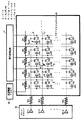
図18に、TFTマトリックスパネルの等価回路の一例を示す。
【0006】
図18において、1はTFT(薄膜トランジスタ)3をマトリックス状に配したTFTマトリックスパネル、4はコンデンサ又は光電変換素子(ここではフォトダイオードなどの容量あるいはMIS(Metal Insulating Semiconductor)型光センサの容量若しくは光導電型光センサと組み合わせられた電荷蓄積コンデンサの容量として示す)、5は信号を転送する転送ライン(Sig line)、6はバイアスライン(Vs line)、7はゲートライン(Vg line)、11はアンプを有する信号処理回路、12は共通電極ドライバ、13はゲートドライバであり、R1,R0はそれぞれ配線抵抗、Aは断線部、Bは短絡部である。
【0007】
尚、図中、c11,c12・・・・c21,c22・・・・c5nはそれぞれコンデンサ又は光電変換素子4を個々に示しており、t11,t12・・・・t21,t22・・・・t5nはそれぞれTFT3を個々に示しており、Vs1,Vs2・・・・Vs5はそれぞれバイアスライン6を個々に示しており、Dr.1,Dr.2・・・・Dr.nは各ゲートラインに対応するゲートドライバを個々に示している。
【0008】
図18に示される半導体装置においては、ゲートドライバ13のDr.1〜Dr.nから複数のゲートライン7(たとえばCr(クロム)配線)に供給されるバイアス電圧により、マトリックス状に配置された複数のTFT(t11〜tmn)3を駆動し、各画素を構成するTFTと対をなす光電変換素子で得られた電気信号を、該光電変換素子c11〜cmnの第1の電極から、複数の転送ライン5(たとえばAl(アルミニウム)配線)を通じて、信号処理回路11へと転送し、これにより各マトリックス素子即ち画素からの信号読出しを行う。
【0009】
また、共通電極ドライバ12に接続された複数のバイアスライン6(たとえばAl配線)に複数の光電変換素子(c11〜cmn)の第2の電極を接続している。
【0010】
図19は、図18のTFTパネルの共通電極ドライバ12によるバイアスライン6へのバイアス印加側とは反対の側のコーナー部のパターン図の一例である。
【0011】
このTFTパネルの製造において、図18に符号Aで示されているように、バイアスラインVs2の断線が発生した際には、コンデンサ又は光電変換素子(c22〜c2n)が共通電極ドライバ12から分離され、このコンデンサ又は光電変換素子が属する画素及びそれより下方の画素は欠陥画素となり、多くの場合はライン状の欠陥が発生する。また、図18に符号Bで示されているように、異物付着等によりバイアスラインとゲートラインとのショートが発生した際には、ショートした双方のラインに所望の電圧がかからないため、バイアスラインとゲートラインに沿って欠陥が発生する。このような欠陥発生は製造歩留まり低下の原因となっていた。
【0012】
本発明の目的は、画素のマトリックス状配列を有する半導体装置の製造工程における配線の断線や上下の金属配線間のショートによる歩留まりの低下を防止し、パネルが大判化し更に画素パターンが微細化しても、半導体装置を良好な歩留まりで製造することができる半導体装置及びその製造方法を提供することにある。
【0013】
更に、本発明の目的は、画素コンデンサ及びTFTを含んでなる画素のマトリックス状配列を有する半導体装置の画素コンデンサ部の開口率を減少させることなしに良好な歩留まりで製造可能な半導体装置及びその製造方法を提供することにある。
【0014】
【課題を解決するための手段】
本発明の上記目的は、複数の画素列を構成するように複数の画素がマトリックス状に配列された光電変換装置であって、
前記複数の画素はそれぞれ、
第1の主電極、第2の主電極、及びこれらの二つの主電極間の電気的導通を制御する制御電極を有する薄膜トランジスタと、
第1の電極及び第2の電極を有し、前記第1の電極が前記薄膜トランジスタの第1の主電極に接続されている光電変換素子と
を備え、
前記光電変換装置は、
複数の画素列のそれぞれに対して設けられた複数の信号転送ラインと、
複数の画素列のそれぞれに対して設けられた複数のバイアスラインであって、該当する画素列を構成する画素の前記光電変換素子の第2の電極に各バイアスラインが接続された複数のバイアスラインと、
奇数列の画素列に対して設けられたバイアスラインの第1の端部を通して、当該画素列を構成する前記光電変換素子の第2の電極に蓄積された電子を除去するために当該第2の電極にバイアスを印加する第1の共通電極ドライバと、
偶数列の画素列に対して設けられたバイアスラインの第1の端部を通して、当該画素列を構成する前記光電変換素子の第2の電極に蓄積された電子を除去するために当該第2の電極にバイアスを印加する第2の共通電極ドライバと、
前記薄膜トランジスタの制御電極に接続されており、前記光電変換素子の第1の電極からの電気信号を当該薄膜トランジスタの第2の主電極と前記信号転送ラインとを通して読み出すことで、暗電流除去のための空読み出しと目的の読み出し信号を得るための本読み出しとを行うゲートドライバと、
奇数列の画素列に対して設けられたバイアスラインの第2の端部同士を電気的に接続する第1の冗長配線と、
偶数列の画素列に対して設けられたバイアスラインの第2の端部同士を電気的に接続する第2の冗長配線と
を備え、
奇数列の画素列を構成する画素に対して前記バイアスの印加、前記空読み出し、及び前記本読み出しを順に行うサイクルと、偶数列の画素列を構成する画素に対して前記バイアスの印加、前記空読み出し、及び前記本読み出しを順に行うサイクルとが半サイクル分ずれており、
前記第1の共通電極ドライバによる前記バイアスの印加と前記第2の共通電極ドライバによる前記バイアスの印加とは異なるタイミングで行われ、
奇数列の画素列における前記空読み出しと偶数列の画素列における前記本読み出しとが同時に行われ、且つ奇数列の画素列における前記本読み出しと偶数列の画素列における前記空読み出しとが同時に行われる
ことを特徴とする光電変換装置により達成される。
【0018】
【発明の実施の形態】
以下、本発明の実施の形態を図面を参照しながら説明する。
【0019】
[実施形態1]
図1は、本発明の実施形態1に関わるTFTマトリックスパネルの等価回路図である。本実施形態は、TFTパネルが光電変換装置に適用された例である。
【0020】
図1において、図18と同じ部材については説明を省略する。尚、本実施形態の場合、符号4は光電変換素子になる。光電変換素子としては、フォトダイオード型又はMIS型の(例えば基板上に電極、絶縁層、光電変換のための半導体層、オーミックコンタクト層(n+ 型半導体層)を少なくとも有する積層構造を有する)光センサを好適に使用することができる。
【0021】
図1においては、冗長配線21が各バイアスラインに共通に設けられている。また、符号14は、図18の信号処理回路11と同様なアンプを有する信号処理回路である。
【0022】
図2は、図1のTFTパネルの共通電極ドライバ12によるバイアスライン6へのバイアス印加側とは反対の側のコーナー部の概略的パターン図である。
【0023】
本実施形態では、図1及び図2に示されているように、各バイアスラインVs1,Vs2,Vs3,・・・・・は、共通電極ドライバ12との接続側とは反対の側の端部どうしが冗長配線21により互いに電気的に接続されている。該冗長配線21は、パネルの絶縁基板の切断により形成されるパネル端部31の近傍に位置している。
【0024】
図3は、本実施形態のTFTマトリックスパネルの製造の際の欠陥及びその修復方法の一例を説明するための等価回路図である。
【0025】
TFTパネルの製造において、図3に符号Aで示されているように、バイアスラインVs2の断線が発生した際には、光電変換素子c22〜c2nには、他の複数のバイアスライン(Vs1,Vs4など)から冗長配線21を介してバイアス電圧が印加されることにより、ライン欠陥とならない。
【0026】
また、光電変換素子c22の欠陥により画素欠陥を生ぜしめた場合には、当該画素のTFT(t22)に対してレーザー照射して光電変換素子c22と転送ラインとを分離することにより、電気的な悪影響を防止することができる。
【0027】
また、図3に符号Bで示されているように、異物付着等によりバイアスラインVs3とゲートラインとのショートが発生した際には、光電変換素子c32に係るバイアスライン方向及びゲートライン方向に関し隣接する部分もしくは当該方向に関する画素全体が欠陥となる。そこで、本実施形態では、ショートしたバイアスラインVs3を、ショート部分を挟む両側においてレーザー照射してショート部分をバイアスラインVs3の他の部分から電気的に分離することにより、バイアスラインとゲートラインとのショートによる欠陥を防止することができる。即ち、光電変換素子c32に係るゲートラインは修復されるし、光電変換素子c32に係るバイアスラインVs3は断線扱いとなるが、光電変換素子c32〜c3nには、他の複数のバイアスライン(Vs1,Vs4など)から冗長配線を介してバイアスが印加されることにより、ライン欠陥とならない。また、ショート部分の付近の光電変換素子の欠陥により画素欠陥を生ぜしめた場合には、当該欠陥画素のTFTに対してレーザー照射して欠陥の光電変換素子と転送ラインとを分離することにより、電気的な悪影響を防止することができる。
【0028】
以上のようにして、本実施形態では、バイアスラインに接続される冗長配線をパネル絶縁基板の端部31の近傍に位置させることで、画素の開口率を殆ど低下させることなしに、バイアスラインの断線やバイアスラインとゲートラインとのショートによる欠陥を修復して、製造歩留まりを向上させることができる。
【0029】
さらに、冗長配線21を設けることにより、共通電極ドライバからの印加バイアスに対する各画素までの配線抵抗を減少させることが可能となる。
【0030】
[実施形態2]
図4は、本発明の実施形態2に関わるTFTマトリックスパネルの概略的等価回路図である。本実施形態は、TFTパネルが光電変換装置に適用された例である。
【0031】
図4において、図18と同じ部材については、図18の説明を参照することとして、ここでは説明を省略する。
【0032】
本実施形態では、共通電極ドライバ12に接続された複数のバイアスライン6に複数の光電変換素子(c11〜cmn)の第2の電極をそれぞれ接続している点は変わらないが、本実施形態では、バイアスライン6を2系統に分割し、2つの共通電極ドライバ12により各系統のバイアスライン6にバイアス電圧を印加可能にしている。
【0033】
本実施形態において、光電変換素子はMIS型のセンサとして説明する。信号転送後、光電変換素子(素子中にコンデンサが形成される)c11〜cmnの第2の電極に蓄積された電子は、n+ 型半導体層(一方の電極を構成する)に共通電極ドライバ12からバイアスを印加することにより除去される。
【0034】
図5は、図4のTFTパネルの共通電極ドライバ12によるバイアスライン6へのバイアス印加側とは反対の側のコーナー部の概略的パターン図である。
【0035】
本実施形態では、図4及び図5に示されているように、各バイアスラインは、共通電極ドライバ12との接続側とは反対の側の端部どうしが冗長配線21−1,21−2により互いに電気的に接続されている。ここで、バイアスライン6は2つの系統に分割されており、各系統ごとに共通電極ドライバ12が別々に設けられており、また各系統ごとに冗長配線21−1,21−2による接続がなされている。即ち、第1系統の複数のバイアスラインは一方の端部が第1の共通電極ドライバに接続されており他方の端部どうしが冗長配線21−1により互いに電気的に接続されており、第2系統の複数のバイアスラインは一方の端部が第2の共通電極ドライバに接続されており他方の端部どうしが冗長配線21−2により互いに電気的に接続されている。
【0036】
冗長配線21−1及び冗長配線21−2は、パネルの絶縁基板の切断により形成されるパネル端部31の近傍に位置している。ここで、画素の配列ピッチをPとしたときに、最外周にある光電変換素子の端部から絶縁基板カッティング時のパネル端部までの距離を、図5に示されているように、転送ライン5と平行方向のカッティングにおいてXとし、ゲートライン7と平行方向のカッティングにおいてYとして、
X<P
Y<P
となるように冗長配線21−1及び冗長配線21−2を配置することにより、本実施形態の光電変換装置をユニットとして複数用いてX方向及び/またはY方向に複数配列して更に大面積の光電変換装置を構成する際の隣接ユニットの互いに隣接する光電変換素子どうしの間隔の増加を防止することができる。
【0037】
図6は図5のC−C′断面図である。図6中、符号80は絶縁基板であり、符号81はCr配線層、符号82は絶縁膜、符号83はi半導体層、符号84はn+ 半導体層、符号85はAl配線層、符号86は保護層、符号87は冗長配線21−1、符号88は冗長配線21−2であり、これらの各薄膜は、光電変換素子及びTFTを形成する成膜プロセスと同時に成膜されたものである。即ち、図6に示されているように、冗長配線21−1は、ゲートラインを形成するCr配線と同時に成膜したCr配線金属層81及びバイアスラインを形成するAl配線と同時に成膜したAl配線金属層85を用いて形成することができ、また、冗長配線21−2は、バイアスラインを形成するAl配線と同時に成膜したAl配線金属層を用いて形成することができる。冗長配線21−1と冗長配線21−2とは、光電変換素子の形成時に成膜された絶縁膜82により電気的に分離されている。これにより、成膜プロセスを増やすことなく冗長配線を形成することができる。
【0038】
図7は、本実施形態のTFTマトリックスパネルの製造の際の欠陥及びその修復方法の一例を説明するための等価回路図である。
【0039】
TFTパネルの製造において、図7に符号Aで示されているように、バイアスラインVs2の断線が発生した際には、光電変換素子c22〜c2nには、他の複数の同系統のバイアスライン(Vs4,Vs6など)から冗長配線21−2を介してバイアス電圧が印加されることにより、ライン欠陥とならない。
【0040】
また、光電変換素子c22が画素欠陥を生ぜしめた場合には、当該画素のTFT(t22)に対してレーザー照射して光電変換素子c22と転送ラインとを分離することにより、電気的な悪影響を防止することができる。
【0041】
また、図7に符号Bで示されているように、異物付着等によりバイアスラインVs3とゲートラインとのショートが発生した際には、光電変換素子c32に係るバイアスライン方向及びゲートライン方向に関し隣接する部分もしくは当該方向に関する全体が欠陥となる。そこで、本実施形態では、ショートしたバイアスラインVs3を、ショート部分を挟む両側においてレーザー照射してショート部分をバイアスラインVs3の他の部分から電気的に分離することにより、バイアスラインとゲートラインとのショートによる欠陥を防止することができる。即ち、画素コンデンサc32に係るゲートラインは修復されるし、光電変換素子c32に係るバイアスラインVs3は断線扱いとなるが、光電変換素子c32〜c3nは、他の複数の同系統のバイアスライン(Vs1,Vs5など)から冗長配線21−1を介してバイアスが印加されることにより、ライン欠陥とならない。また、ショート部分の付近のコンデンサが画素欠陥を生ぜしめた場合には、当該欠陥画素のTFTに対してレーザー照射して欠陥コンデンサと転送ラインとを分離することにより、電気的な悪影響を防止することができる。
【0042】
本実施形態では、バイアスラインを2系統に分割し、2つの共通電極ドライバ12によりそれぞれバイアスを印加して各系統ごとに別駆動し、且つ冗長配線もこのバイアスラインの各系統ごとに分離して接続している。これにより、マトリックス状に配列された光電変換素子を2系列で駆動させることが可能となり、1サイクルの信号読出し時の解像度を1/2にすることにより、信号処理の速度を約2倍とすることができる。MIS型の光電変換素子では、バイアスラインによりバイアスを印加して信号を読み込むまでの間に暗電流が発生するために、暗電流除去のための「空読出し」をした後に目的とする読出し信号を得る「本読出し」をすることが好ましい。この場合、1サイクルの信号読み出し時間が長くなるが、これは以下のようにして補うことが可能である。
【0043】
図8(a),(b)に、バイアスラインを1系統とした時及び2系統とした時のバイアスラインへのバイアス印加タイミングと空読出しタイミング及び本読出しタイミングの一例を示す。
【0044】
図8(a)はバイアスラインを1系統とした時を示し、1サイクルの読出しに時間t1を要する。これに対して、図8(b)はバイアスラインを2系統とした時を示し、第1系統と第2系統のバイアスタイミングを別駆動で印加し、第1系統の空読出し時に得られる第2系統からの信号を本読出しとし、逆に第1系統の本読出し時に得られる第2系統からの信号を空読出しとすることにより、解像度が1/2ではあるが約半分の時間t1/2で信号読出しを行うことができる。
【0045】
もちろん、本実施形態においても、2系統のバイアスラインに対して同じバイアスタイミングを印加することで、従来と同様の解像度及び所要時間での読出しを行うことも可能である。
【0046】
また、本実施形態では、絶縁基板上に共通電極ドライバからのバイアス印加ラインを複数本設けて、複数の経路のバイアスラインを介してバイアス電圧を印加することにより、共通電極ドライバから各光電変換素子の第2の電極までの配線抵抗(R1等)を低減することができ、光電変換素子の第2の電極に印加するバイアス波形を均一なものとなし、特性を向上させることが可能である。
【0047】
本実施形態でも、実施形態1と同様に、冗長配線はパネル絶縁基板の端部31の近傍に位置しているので、光電変換素子の開口率を殆ど低下させることなしに、バイアスラインの断線やバイアスラインとゲートラインとのショートによる欠陥を修復して、製造歩留まりを向上させることができる。
【0048】
以上の2つの実施形態では、TFTマトリックスパネルはm×n個のマトリックスを構成しているが、実施形態1ではm≧2,n≧1が可能であり、実施形態2ではm≧4,n≧1が可能である。
【0049】
[実施形態3]
図9は、本発明の実施形態3に関わるTFTマトリックスパネルの概略的等価回路図である。本実施形態は、TFTパネルが光電変換装置に適用された例である。
【0050】
ゲートドライバ13のDr.1〜Dr.nから複数のゲートライン7に供給されるバイアス電圧により、マトリックス状に配置された複数のTFT(t11〜tmn)3を駆動し、各画素を構成するTFTと対をなす光電変換素子で得られた電気信号を、該光電変換素子c11〜cmnの第1の電極から、複数の転送ライン5を通じて、信号処理回路14へと転送し、これにより各マトリックス素子即ち画素からの信号読出しを行う。
【0051】
また、共通電極ドライバ12に接続された複数のバイアスライン6に複数の光電変換素子(c11〜cmn)の第2の電極を接続している。本実施形態では、バイアスラインを複数の系統に分割し、複数の共通電極ドライバ12により各系統のバイアスラインにバイアス電圧を印加するようにしている。
【0052】
光電変換素子はMIS型のセンサであり、信号転送後、光電変換素子c11〜cmnの第2の電極に蓄積された電子は、n+ 型半導体層に共通電極ドライバ12からバイアス電圧を印加することにより除去される。以下この動作をリフレッシュと呼ぶ。
【0053】
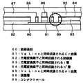
図10は、図9のTFTパネルの4系統の場合の共通電極ドライバ12によるバイアスライン6へのバイアス印加側とは反対の側のコーナー部のパターン図である。
【0054】
本実施形態では、図9及び図10に示されているように、各バイアスラインは、共通電極ドライバ12との接続側とは反対の側の端部どうしが冗長配線21−1〜21−4により互いに電気的に接続されている。ここで、バイアスラインは複数の系統(k系統)に分割されており、また各系統ごとに冗長配線による接続がなされている。即ち、第1系統の複数のバイアスラインは一方の端部が第1の共通電極ドライバに接続されており他方の端部どうしが冗長配線21−1により互いに電気的に接続されており、同様に第2系統から第k系統の複数のバイアスラインは一方の端部がそれぞれ第2から第kの共通電極ドライバに接続されており他方の端部どうしが冗長配線21−2から冗長配線21−kにより夫々互いに電気的に接続されている。
【0055】
また、冗長配線21−1から冗長配線21−kは、パネルの絶縁基板の切断により形成されるパネル端部31の近傍に位置している。
【0056】
図11は図10のZ−Z′における模式的断面図である。図11中、符号80は絶縁基板であり、符号81はCr配線層、符号82は絶縁膜、符号83はi半導体層、符号84はn+ 半導体層、符号85はAl配線層、符号86は保護層、符号87は冗長配線21−1、符号88は冗長配線21−4である。符号85のAl配線層と符号81のCr配線層は符号89のコンタクトホール(CH)を介して接続されているが、ここには接続抵抗が発生する。
【0057】
バイアスラインがk系統の場合、冗長配線21−1にはk−1個のクロス部が存在するため、コンタクトホールCHは2(k−1)個となる。また、冗長配線21−2にはk−2個のクロス部が存在するため、コンタクトホールCHは2(k−2)個となり、冗長配線毎にコンタクトホールCHの数が異なる。
【0058】
ここで4系統の場合について考えてみると、冗長配線21−1のクロス部は3個、冗長配線21−2のクロス部は2個、冗長配線21−3のクロス部は1個となり、冗長配線21−4にはクロス部は存在しない。この時、コンタクトホールCHは先に述べたように接続抵抗を持つため、系統毎の配線抵抗が異なる。配線抵抗が異なると、リフレッシュ時の時定数の差によると思われる出力(特に暗出力)の違いが各系統毎に発生する場合がある。この様な周期的な出力の差は認識しやすく、大きな問題となる場合がある。
【0059】
そこで本実施形態では、図10のように全ての冗長配線に同一形態、同一個数のクロス部、コンタクトホールCHを設け、配線抵抗を同等にすることにより、配線の断線や上下の金属配線間のショートによる歩留りの低下を防止できるだけでなく、パネル内における特性の均一化が可能となり、その結果パネルのS/Nをも向上することができる。
【0060】
[実施形態4]
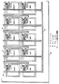
図9に示したTFTマトリックスパネルを4枚用いて1つの光電変換装置を構成する一例を示す。
【0061】
図12は、図9のTFTパネル4枚の夫々の1つの角部を集合させて配置した場合の各パネルコーナー部の模式的パターン図である。
【0062】
実施形態1〜3によれば、冗長配線をパネル端部に配置しており、この時配置のスペースが必要となる。ここで図12のように画素の配列ピッチをfとすると、パネルを貼り合せる場合にはつなぎ目を画像補正するため、つなぎ目のマージンは1画素分、即ち各パネルの最外周に配置された画素間(光電変換部の重心間)の距離wは、w=2fである事が望ましい。また、パネルの貼り合せは光電変換部の重心を基準に行う。
【0063】
図13(a),(b)は、本実施形態における光電変換部の重心を説明する概略的パターン図である。
【0064】
図13(a)の場合には、TFTの位置等により光電変換部の重心がパネル端部から離れる。この時パネル端部と配線を含めたデバイス端部の距離aは、信頼性上及び切断マージンとして一定量必要である。その結果、パネル端部間の距離dは小さくなり、冗長配線(特に複数になった場合)の配線が困難になることがある。
【0065】
そこで本実施形態では、図13(b)の様に、TFTをパネル端部から離れた位置に配置する事等により、光電変換部の重心をパネル端部に近付ける事により、aがある一定量に規定されたとしても、dを大きくとることができるようにした。その結果冗長配線が複数になっても、wやdを変えることなくそれら全てを配置できる十分なエリア、即ちパネル端部と配線を含めたデバイス端部の距離aを設ける事が可能となる。
【0066】
[実施形態5]
本実施形態は複数画素の行列を同一パネル内で複数の領域(ここでは上下)に分けて構成するものである。図14に概略的等価回路図を示す。本実施形態では、共通電極ドライバ12を基体の図中上下両側に配置し、基体の図中左側より各画素を駆動させる構成である。これは、更なる大面積化及び高速動作などを実現する上で有用である。
【0067】
尚、図中、14は信号処理回路、12は共通電極ドライバ、13はTFTドライバ(ゲートドライバ)、21は冗長配線である。
【0068】
また、図15に、基体の上下方向の中央部に配されている冗長配線部を拡大した模式的パターン図を示す。図中、点cはセンサ重心、fは画素ピッチである。上下方向のパネル中央に関して、上方のセンサと下方のセンサとで配列の向きを逆にし、いずれもセンサ重心がパネル中央に近くなるように配列することで、パネル中央のクリアランスK0 は、上方または下方のセンサ間クリアランスKよりも幅広にすることができ、画像の劣化を防止できる。よって、そのスペースを利用して冗長配線21を適切に配置することが可能となる。
【0069】
上述の実施形態の光電変換装置は非破壊検査や医療などに用いられるX線検査の検出用センサとして利用することができる。以下、医療用を例にあげて適用例を説明する。非破壊検査は患者を被検査物に代えて置きかえればよい。
【0070】
図16(a),(b)は本発明をX線検出用の光電変換装置に適用した場合の模式的構成図及び模式的断面図である。
【0071】
光電変換素子とTFTは、上述したように、センサ基板6011内に複数個形成され、これらにはシフトレジスタSR1と検出用集積回路ICとが実装されたフレキシブル回路基板6010が接続されている。フレキシブル回路基板6010の逆側は回路基板PCB1,PCB2に接続されている。前記センサ基板6011の複数枚又は1枚が基台6012の上に接着され大型の光電変換装置を構成する。基台6012の下には処理回路6018内のメモリ6014をX線から保護するため鉛板6013が実装されている。センサ基板6011上にはX線を可視光に変換するための波長変換体として蛍光体6030たとえばCsIが、塗布または蒸着あるいは貼り付けされている。光電変換装置は図16(b)に示されるように全体をカーボンファイバー製のケース6020に収納している。
【0072】
図17は本発明の光電変換装置をX線診断システムへ応用した例を示すものである。
【0073】
X線チューブ6050で発生したX線6060は患者あるいは被験者6061の胸部6062を透過し、蛍光体を上部に実装した光電変換装置6040に入射する。この入射したX線には患者6061の体内部の情報が含まれている。X線の入射に対応して蛍光体は発光し、これを光電変換して電気的情報を得る。この情報はディジタルに変換されイメージプロセッサ6070により画像処理され制御室のディスプレイ6080で観察できる。
【0074】
また、この情報は電話回線6090等の伝送手段により遠隔地へ転送でき、別の場所のドクタールームなどのディスプレイ6081に表示もしくは光ディスク等の保存手段に保存することができ、遠隔地の医師が診断することも可能である。またフィルムプロセッサ6100によりフィルム6110に記録することもできる。
【0075】
【発明の効果】
以上に説明したように、本発明によれば、共通電極ドライバとの接続側とは反対の側においてバイアスラインの端部どうしを冗長配線により互いに電気的に接続することにより、光電変換素子やコンデンサ及びTFTを含んでなる画素のマトリックス状配列を有する半導体装置の製造工程における配線の断線や上下の金属配線間のショートによる歩留まりの低下を防止し、パネルが大判化し更に画素パターンが微細化しても、半導体装置を良好な歩留まりで製造することができる。
【0076】
更に、本発明によれば、光電変換素子やコンデンサ及びTFTを含んでなる画素のマトリックス状配列を有する半導体装置の画素部の開口率を減少させることなしに良好な歩留まりで半導体装置を製造することが可能である。
【0077】
尚、上記実施形態において、光電変換素子以外の画素素子としてのコンデンサを有する場合も同様な考え方を適用してもよい。又、本発明は、本発明の主旨の範囲内において、適宜変形、組合わせが可能であることはいうまでもない。
【図面の簡単な説明】
【図1】本発明の実施形態1に関わるTFTマトリックスパネルの等価回路図である。
【図2】図1のTFTパネルの共通電極ドライバによるバイアスラインへのバイアス印加側とは反対の側のコーナー部の概略的パターン図である。
【図3】本発明の実施形態1のTFTマトリックスパネルの製造の際の欠陥及びその修復方法の一例を説明するための等価回路図である。
【図4】本発明の実施形態2に関わるTFTマトリックスパネルの等価回路図である。
【図5】図4のTFTパネルの共通電極ドライバによるバイアスラインへのバイアス印加側とは反対の側のコーナー部の概略的パターン図である。
【図6】図5のC−C′断面図である。
【図7】本発明の実施形態2のTFTマトリックスパネルの製造の際の欠陥及びその修復方法の一例を説明するための等価回路図である。
【図8】バイアスラインを1系統とした時及び2系統とした時のバイアスラインへのバイアス印加タイミングと空読出しタイミング及び本読出しタイミングの一例を示す図である。
【図9】本発明の実施形態3に関わるTFTマトリックスパネルの概略的等価回路図である。
【図10】図9のTFTパネルの4系統の場合の共通電極ドライバによるバイアスラインへのバイアス印加側とは反対の側のコーナー部のパターン図である。
【図11】図10のZ−Z′における模式的断面図である。
【図12】図9のTFTパネル4枚の夫々の1つの角部を集合させて配置した場合の各パネルコーナー部の模式的パターン図である。
【図13】光電変換部の重心を説明する概略的パターン図である。
【図14】複数画素の行列を同一パネル内で複数の領域に分けて構成した場合の概略的等価回路図である。
【図15】基体の上下方向の中央部に配されている冗長配線部を拡大した模式的パターン図である。
【図16】本発明をX線検出用の光電変換装置に適用した場合の模式的構成図及び模式的断面図である。
【図17】本発明の光電変換装置をX線診断システムへ応用した例を示す図である。
【図18】TFTマトリックスパネルの等価回路図である。
【図19】図18のTFTパネルの共通電極ドライバによるバイアスラインへのバイアス印加側と反対の側のコーナー部のパターン図である。
【符号の説明】
1 TFTマトリックスパネル
2 光電変換装置
3 TFT
4 コンデンサ
5 転送ライン(Sig line)
6 バイアスライン(Vs line)
7 ゲートライン(Vg line)
11 信号処理回路
12 共通電極ドライバ
13 ゲートドライバ
14 信号処理回路
21 冗長配線
21−1,21−2,・・・・ 冗長配線
31 絶縁基板cut時のパネル端部
80 絶縁基板
81 Cr配線層
82 絶縁膜
83 i半導体層
84 n+ 半導体層
85 Al配線層
86 保護層
87,88 冗長配線[0001]
BACKGROUND OF THE INVENTION
The present invention relates to a semiconductor device and a manufacturing method thereof, for example, a semiconductor device having a thin film transistor (TFT) matrix panel suitably used for forming a liquid crystal display device or a photoelectric conversion device and a manufacturing method thereof.
[0002]
[Prior art and problems to be solved by the invention]
Conventionally, a display unit of a display device such as a liquid crystal panel and a reading unit of a photoelectric conversion device such as an area sensor are configured by a large number of display pixels and reading pixels arranged in an XY matrix, and a signal input to each pixel or It is widely performed that signal readout from each pixel is performed by an XY matrix driving method through a TFT provided for each pixel. A display pixel of a display device can be formed using a liquid crystal display element in which liquid crystal is interposed between a pair of electrodes at least one of which is transparent, and a reading pixel of a photoelectric conversion device is a semiconductor between a pair of electrodes. A photoelectric conversion element in which a photoelectric conversion layer is interposed can be used.
[0003]
TFT panels having such a matrix arrangement of pixels with TFTs have been rapidly increasing in size in recent years. This is due to the influence of development of a manufacturing technique of a liquid crystal display device using a TFT panel and use of an area sensor having a photoelectric conversion element in various fields (for example, application to an X-ray imaging apparatus). In addition, along with this trend toward larger sizes, pixel pattern arrangement pitches are becoming finer. With these panel enlargement and pixel miniaturization, the yield in the TFT panel manufacturing process is reduced. Possible causes include the following:
(1) As the panel size increases, the wiring distance per panel increases, and the disconnection probability increases accordingly.
(2) As the pixel pattern of the panel is further miniaturized, the area of the TFT and wiring cross portion per panel increases, so the short-circuit probability between the upper and lower metal wirings increases.
(3) Electrostatic breakdown (ESD). That is, as the panel becomes larger, the area that can be contacted with the outside increases, and the amount of static electricity is likely to increase, thus increasing the probability of occurrence of defects due to ESD.
[0004]
By solving these technical problems, an improvement in yield is ensured. However, among these causes, (1) can be solved by increasing the wiring width. On the contrary, (2) reduces the area of the cross portion between the upper and lower metal wires, that is, the cross portion. This can be solved by reducing the wiring width. Further, by increasing the thickness of the wiring, the inter-wiring capacitance formed between the upper and lower metal wirings increases, and the sensitivity of the transferred signal decreases. In addition, it is conceivable to improve the yield by forming a redundant circuit. However, when the aperture ratio of the pixel capacitor portion is reduced by this redundant circuit, there may be a problem that the sensitivity is reduced. Thus, the design of the wiring width is very difficult.
[0005]
FIG. 18 shows an example of an equivalent circuit of a TFT matrix panel.
[0006]
In FIG. 18, 1 is a TFT matrix panel in which TFTs (thin film transistors) 3 are arranged in a matrix, 4 is a capacitor or a photoelectric conversion element (here, a capacitance such as a photodiode or a capacitance or light of a MIS (Metal Insulating Semiconductor) type optical sensor. 5 is a transfer line (Sig line) for transferring a signal, 6 is a bias line (Vs line), 7 is a gate line (Vg line), and 11 is a transfer line (Sig line) combined with a conductive photosensor. A signal processing circuit having an amplifier, 12 is a common electrode driver, 13 is a gate driver, R1 and R0 are wiring resistances, A is a disconnected portion, and B is a short-circuited portion.
[0007]
In the figure, c11, c12... C21, c22... C5n respectively indicate capacitors or
[0008]
In the semiconductor device shown in FIG. 1-Dr. A plurality of TFTs (t11 to tmn) 3 arranged in a matrix are driven by a bias voltage supplied from n to a plurality of gate lines 7 (for example, Cr (chromium) wiring), and are paired with TFTs constituting each pixel. The electric signal obtained by the photoelectric conversion element forming the above is transferred from the first electrodes of the photoelectric conversion elements c11 to cmd to the
[0009]
Further, the second electrodes of the plurality of photoelectric conversion elements (c11 to cmd) are connected to the plurality of bias lines 6 (for example, Al wiring) connected to the
[0010]
FIG. 19 is an example of a pattern diagram of a corner portion on the side opposite to the side of bias application to the
[0011]
In the manufacture of this TFT panel, as indicated by the symbol A in FIG. 18, when the disconnection of the bias line Vs2 occurs, the capacitor or the photoelectric conversion element (c22 to c2n) is separated from the
[0012]
An object of the present invention is to prevent a decrease in yield due to disconnection of a wiring or a short circuit between upper and lower metal wirings in a manufacturing process of a semiconductor device having a matrix arrangement of pixels, and even if a panel is enlarged and a pixel pattern is further miniaturized. Another object of the present invention is to provide a semiconductor device and a method for manufacturing the same that can manufacture the semiconductor device with a good yield.
[0013]
Furthermore, an object of the present invention is to provide a semiconductor device that can be manufactured with a good yield without reducing the aperture ratio of the pixel capacitor portion of the semiconductor device having a matrix arrangement of pixels including pixel capacitors and TFTs, and its manufacture. It is to provide a method.
[0014]
[Means for Solving the Problems]
The above object of the present invention is toA photoelectric conversion device in which a plurality of pixels are arranged in a matrix so as to constitute a plurality of pixel columns,
Each of the plurality of pixels is
A thin film transistor having a first main electrode, a second main electrode, and a control electrode for controlling electrical conduction between the two main electrodes;
A photoelectric conversion element having a first electrode and a second electrode, wherein the first electrode is connected to a first main electrode of the thin film transistor;
With
The photoelectric conversion device
A plurality of signal transfer lines provided for each of the plurality of pixel columns;
A plurality of bias lines provided for each of the plurality of pixel columns, wherein the bias lines are connected to the second electrodes of the photoelectric conversion elements of the pixels constituting the corresponding pixel column. When,
In order to remove the electrons accumulated in the second electrode of the photoelectric conversion element constituting the pixel column through the first end of the bias line provided for the odd-numbered pixel column, A first common electrode driver for applying a bias to the electrodes;
In order to remove the electrons accumulated in the second electrode of the photoelectric conversion element constituting the pixel column through the first end of the bias line provided for the pixel column of the even column, A second common electrode driver for applying a bias to the electrodes;
It is connected to the control electrode of the thin film transistor, and an electric signal from the first electrode of the photoelectric conversion element is read through the second main electrode of the thin film transistor and the signal transfer line, thereby removing dark current. A gate driver that performs empty reading and main reading to obtain a target reading signal;
A first redundant wiring that electrically connects the second ends of the bias lines provided for the odd-numbered pixel columns;
A second redundant wiring for electrically connecting the second ends of the bias lines provided for the even-numbered pixel columns;
With
A cycle in which the application of the bias, the empty reading, and the main reading are sequentially performed on the pixels configuring the odd-numbered pixel columns, and the application of the bias to the pixels configuring the even-numbered pixel columns, the empty The cycle in which reading and the main reading are sequentially performed are shifted by a half cycle,
The application of the bias by the first common electrode driver and the application of the bias by the second common electrode driver are performed at different timings,
The empty reading in the odd-numbered pixel columns and the main reading in the even-numbered pixel columns are simultaneously performed, and the main reading in the odd-numbered pixel columns and the empty reading in the even-numbered pixel columns are simultaneously performed.
Photoelectric conversion deviceIs achieved.
[0018]
DETAILED DESCRIPTION OF THE INVENTION
Embodiments of the present invention will be described below with reference to the drawings.
[0019]
[Embodiment 1]
FIG. 1 is an equivalent circuit diagram of a TFT matrix panel according to
[0020]
In FIG. 1, the description of the same members as those in FIG. 18 is omitted. In the present embodiment,
[0021]
In FIG. 1, the
[0022]
FIG. 2 is a schematic pattern diagram of a corner portion on the side opposite to the bias application side to the
[0023]
In this embodiment, as shown in FIGS. 1 and 2, each of the
[0024]
FIG. 3 is an equivalent circuit diagram for explaining an example of a defect in manufacturing the TFT matrix panel of the present embodiment and a method for repairing the defect.
[0025]
In the manufacture of the TFT panel, as shown by the symbol A in FIG. 3, when the disconnection of the bias line Vs2 occurs, the photoelectric conversion elements c22 to c2n include other bias lines (Vs1, Vs4). Etc.), a line defect is not caused by applying a bias voltage via the
[0026]
In addition, when a pixel defect is caused by a defect in the photoelectric conversion element c22, the TFT (t22) of the pixel is irradiated with a laser to separate the photoelectric conversion element c22 from the transfer line. Adverse effects can be prevented.
[0027]
3, when a short circuit occurs between the bias line Vs3 and the gate line due to adhesion of foreign matter or the like, adjacent to the bias line direction and the gate line direction related to the photoelectric conversion element c32. The part to be processed or the entire pixel in the direction becomes a defect. Therefore, in this embodiment, the shorted bias line Vs3 is irradiated with laser on both sides of the shorted portion to electrically isolate the shorted portion from the other portions of the bias line Vs3, whereby the bias line and the gate line are separated. Defects due to short-circuits can be prevented. That is, the gate line related to the photoelectric conversion element c32 is repaired and the bias line Vs3 related to the photoelectric conversion element c32 is handled as a disconnection, but the photoelectric conversion elements c32 to c3n include other bias lines (Vs1, Vs1, When a bias is applied from the Vs4 etc. via the redundant wiring, no line defect occurs. In addition, when a pixel defect is caused by a defect in the photoelectric conversion element in the vicinity of the short portion, the defective photoelectric conversion element and the transfer line are separated by laser irradiation to the TFT of the defective pixel, Electrical adverse effects can be prevented.
[0028]
As described above, in the present embodiment, the redundant wiring connected to the bias line is positioned in the vicinity of the
[0029]
Furthermore, by providing the
[0030]
[Embodiment 2]
FIG. 4 is a schematic equivalent circuit diagram of a TFT matrix panel according to
[0031]
In FIG. 4, the same members as those in FIG. 18 are referred to the description of FIG.
[0032]
In the present embodiment, the second electrodes of the plurality of photoelectric conversion elements (c11 to cmn) are connected to the plurality of
[0033]
In the present embodiment, the photoelectric conversion element will be described as a MIS type sensor. After the signal transfer, electrons accumulated in the second electrodes of the photoelectric conversion elements (capacitors are formed in the elements) c11 to cmn are n+It is removed by applying a bias from the
[0034]
FIG. 5 is a schematic pattern diagram of a corner portion on the side opposite to the bias application side to the
[0035]
In this embodiment, as shown in FIGS. 4 and 5, each bias line has redundant wirings 21-1 and 21-2 at the ends opposite to the connection side with the
[0036]
The redundant wiring 21-1 and the redundant wiring 21-2 are located in the vicinity of the
X <P
Y <P
By arranging the redundant wiring 21-1 and the redundant wiring 21-2 so that a plurality of photoelectric conversion devices of this embodiment are used as a unit, a plurality of the photoelectric conversion devices are arranged in the X direction and / or the Y direction. It is possible to prevent an increase in the interval between adjacent photoelectric conversion elements of adjacent units when configuring the photoelectric conversion device.
[0037]
6 is a cross-sectional view taken along the line CC ′ of FIG. In FIG. 6,
[0038]
FIG. 7 is an equivalent circuit diagram for explaining an example of a defect in manufacturing the TFT matrix panel of this embodiment and a method for repairing the defect.
[0039]
In the manufacture of the TFT panel, as shown by the symbol A in FIG. 7, when the disconnection of the bias line Vs <b> 2 occurs, the photoelectric conversion elements c <b> 22 to c <b> 2 n have a plurality of other bias lines of the same system ( Vs4, Vs6, etc.) are applied via the redundant wiring 21-2, so that no line defect occurs.
[0040]
When the photoelectric conversion element c22 causes a pixel defect, the TFT (t22) of the pixel is irradiated with a laser to separate the photoelectric conversion element c22 and the transfer line, thereby causing an adverse electrical effect. Can be prevented.
[0041]
In addition, as indicated by a symbol B in FIG. 7, when a short circuit between the bias line Vs3 and the gate line occurs due to adhesion of foreign matter or the like, the bias line direction and the gate line direction related to the photoelectric conversion element c32 are adjacent to each other. The part to be performed or the whole in the direction becomes a defect. Therefore, in this embodiment, the shorted bias line Vs3 is irradiated with laser on both sides of the shorted portion to electrically isolate the shorted portion from the other portions of the bias line Vs3, whereby the bias line and the gate line are separated. Defects due to short-circuits can be prevented. That is, the gate line related to the pixel capacitor c32 is repaired and the bias line Vs3 related to the photoelectric conversion element c32 is treated as a disconnection, but the photoelectric conversion elements c32 to c3n are connected to a plurality of other bias lines (Vs1) of the same system. , Vs5, etc.) through the redundant wiring 21-1, a line defect does not occur. In addition, when a capacitor near the short-circuited portion causes a pixel defect, the TFT of the defective pixel is irradiated with a laser to separate the defective capacitor from the transfer line, thereby preventing an electrical adverse effect. be able to.
[0042]
In this embodiment, the bias line is divided into two systems, biases are respectively applied by the two
[0043]
FIGS. 8A and 8B show an example of bias application timing to the bias line, empty read timing, and main read timing when the bias line is one system and two systems.
[0044]
FIG. 8A shows a case where the bias line is one system, and it takes time t1 to read out one cycle. On the other hand, FIG. 8B shows the case where the bias lines are two systems, and the second system obtained when the first system and the second system are biased by applying the bias timings of the first system and the second system separately. By setting the signal from the system as the main reading and conversely, the signal from the second system obtained at the time of the main reading of the first system is set as the idle reading, so that the resolution is ½ but at about half time t1 / 2. Signal readout can be performed.
[0045]
Of course, also in the present embodiment, it is possible to perform readout with the same resolution and required time as before by applying the same bias timing to the two bias lines.
[0046]
In the present embodiment, a plurality of bias application lines from the common electrode driver are provided on the insulating substrate, and a bias voltage is applied through the bias lines of the plurality of paths, so that each photoelectric conversion element is connected from the common electrode driver. The wiring resistance (R1 and the like) to the second electrode can be reduced, the bias waveform applied to the second electrode of the photoelectric conversion element can be made uniform, and the characteristics can be improved.
[0047]
Also in the present embodiment, as in the first embodiment, the redundant wiring is located in the vicinity of the
[0048]
In the above two embodiments, the TFT matrix panel constitutes an m × n matrix, but in the first embodiment, m ≧ 2, n ≧ 1 is possible, and in the second embodiment, m ≧ 4, n ≧ 1 is possible.
[0049]
[Embodiment 3]
FIG. 9 is a schematic equivalent circuit diagram of a TFT matrix panel according to
[0050]
Dr. of the
[0051]
Further, the second electrodes of the plurality of photoelectric conversion elements (c11 to cmn) are connected to the plurality of
[0052]
The photoelectric conversion element is a MIS type sensor, and after the signal transfer, the electrons accumulated in the second electrodes of the photoelectric conversion elements c11 to cmn are n+It is removed by applying a bias voltage from the
[0053]
FIG. 10 is a pattern diagram of the corner portion on the side opposite to the bias application side to the
[0054]
In this embodiment, as shown in FIG. 9 and FIG. 10, each bias line has redundant wirings 21-1 to 21-4 at the ends opposite to the connection side to the
[0055]
Further, the redundant wiring 21-1 to the redundant wiring 21-k are located in the vicinity of the
[0056]
FIG. 11 is a schematic cross-sectional view taken along the line ZZ ′ of FIG. In FIG. 11,
[0057]
When the bias line is k systems, the redundant wiring 21-1 has k-1 cross portions, and thus there are 2 (k-1) contact holes CH. Further, since k-2 cross portions exist in the redundant wiring 21-2, the number of contact holes CH is 2 (k-2), and the number of contact holes CH is different for each redundant wiring.
[0058]
Considering the case of four systems, there are three cross sections of the redundant wiring 21-1, two cross sections of the redundant wiring 21-2, and one cross section of the redundant wiring 21-3. There is no cross portion in the wiring 21-4. At this time, since the contact hole CH has the connection resistance as described above, the wiring resistance for each system differs. If the wiring resistance is different, a difference in output (particularly dark output) that may be caused by a difference in time constant during refresh may occur in each system. Such a periodic output difference is easy to recognize and may cause a serious problem.
[0059]
Therefore, in the present embodiment, as shown in FIG. 10, all redundant wirings are provided with the same form, the same number of cross portions, and contact holes CH, and the wiring resistances are made equal, so that the wiring breaks or between the upper and lower metal wirings. Not only can the yield be reduced due to a short circuit, but also the characteristics in the panel can be made uniform, and as a result, the S / N of the panel can be improved.
[0060]
[Embodiment 4]
An example of forming one photoelectric conversion device using four TFT matrix panels shown in FIG.
[0061]
FIG. 12 is a schematic pattern diagram of each panel corner portion when one corner portion of each of the four TFT panels of FIG. 9 is assembled.
[0062]
According to the first to third embodiments, the redundant wiring is arranged at the end of the panel. At this time, a space for the arrangement is required. Here, when the pixel arrangement pitch is f as shown in FIG. 12, when joining the panels, the joint image is corrected so that the margin of the joint is one pixel, that is, between the pixels arranged on the outermost periphery of each panel. The distance w (between the centroids of the photoelectric conversion units) is preferably w = 2f. In addition, the panels are bonded based on the center of gravity of the photoelectric conversion unit.
[0063]
FIGS. 13A and 13B are schematic pattern diagrams illustrating the center of gravity of the photoelectric conversion unit in the present embodiment.
[0064]
In the case of FIG. 13A, the center of gravity of the photoelectric conversion unit moves away from the panel end depending on the position of the TFT and the like. At this time, the distance a between the panel end and the device end including the wiring needs a certain amount for reliability and as a cutting margin. As a result, the distance d between the panel ends becomes small, and redundant wiring (particularly when there are a plurality of wirings) may be difficult.
[0065]
Therefore, in the present embodiment, as shown in FIG. 13B, by arranging the TFT at a position away from the panel end, and by bringing the center of gravity of the photoelectric conversion unit closer to the panel end, a has a certain amount. Even if it is prescribed | regulated, it was made to be able to take d large. As a result, even when there are a plurality of redundant wirings, it is possible to provide a sufficient area where all of them can be arranged without changing w and d, that is, a distance a between the panel end and the device end including the wiring.
[0066]
[Embodiment 5]
In this embodiment, a matrix of a plurality of pixels is divided into a plurality of regions (here, upper and lower) in the same panel. FIG. 14 shows a schematic equivalent circuit diagram. In the present embodiment, the
[0067]
In the figure, 14 is a signal processing circuit, 12 is a common electrode driver, 13 is a TFT driver (gate driver), and 21 is a redundant wiring.
[0068]
Further, FIG. 15 shows a schematic pattern diagram in which the redundant wiring portion arranged in the central portion in the vertical direction of the base is enlarged. In the figure, point c is the sensor center of gravity, and f is the pixel pitch. With respect to the center of the panel in the vertical direction, the upper sensor and the lower sensor are reversed in the direction of the array, and the center of sensor is arranged so that the center of gravity of the sensor is close to the panel center.0Can be wider than the upper or lower inter-sensor clearance K, and image deterioration can be prevented. Therefore, the
[0069]
The photoelectric conversion device of the above-described embodiment can be used as a detection sensor for X-ray inspection used for nondestructive inspection or medical treatment. Hereinafter, application examples will be described taking medical use as an example. Nondestructive inspection may be performed by replacing a patient with an object to be inspected.
[0070]
16A and 16B are a schematic configuration diagram and a schematic cross-sectional view when the present invention is applied to a photoelectric conversion device for X-ray detection.
[0071]
As described above, a plurality of photoelectric conversion elements and TFTs are formed in the
[0072]
FIG. 17 shows an example in which the photoelectric conversion device of the present invention is applied to an X-ray diagnostic system.
[0073]
X-rays 6060 generated by the X-ray tube 6050 pass through the
[0074]
This information can be transferred to a remote place by transmission means such as a
[0075]
【The invention's effect】
As described above, according to the present invention, the ends of the bias lines are electrically connected to each other by the redundant wiring on the side opposite to the connection side with the common electrode driver. In addition, it is possible to prevent a decrease in yield due to disconnection of wiring or a short circuit between upper and lower metal wirings in a manufacturing process of a semiconductor device having a matrix arrangement of pixels including TFTs, and even if a panel is enlarged and a pixel pattern is further miniaturized. The semiconductor device can be manufactured with a good yield.
[0076]
Furthermore, according to the present invention, a semiconductor device can be manufactured with a good yield without reducing the aperture ratio of the pixel portion of a semiconductor device having a matrix arrangement of pixels including photoelectric conversion elements, capacitors, and TFTs. Is possible.
[0077]
In the above embodiment, the same concept may be applied to the case where a capacitor is used as a pixel element other than the photoelectric conversion element. Needless to say, the present invention can be appropriately modified and combined within the scope of the gist of the present invention.
[Brief description of the drawings]
FIG. 1 is an equivalent circuit diagram of a TFT matrix panel according to
2 is a schematic pattern diagram of a corner portion on a side opposite to a bias application side to a bias line by a common electrode driver of the TFT panel of FIG.
FIG. 3 is an equivalent circuit diagram for explaining an example of a defect in manufacturing the TFT matrix panel according to
FIG. 4 is an equivalent circuit diagram of a TFT matrix panel according to
5 is a schematic pattern diagram of a corner portion on a side opposite to a bias application side to a bias line by a common electrode driver of the TFT panel of FIG.
6 is a cross-sectional view taken along the line CC ′ of FIG.
FIG. 7 is an equivalent circuit diagram for explaining an example of a defect in manufacturing the TFT matrix panel according to
FIG. 8 is a diagram illustrating an example of bias application timing, empty read timing, and main read timing to a bias line when the bias line is one system and two systems.
FIG. 9 is a schematic equivalent circuit diagram of a TFT matrix panel according to
10 is a pattern diagram of a corner portion on a side opposite to a side of applying a bias to a bias line by a common electrode driver in the case of the four systems of the TFT panel of FIG.
11 is a schematic cross-sectional view taken along the line ZZ ′ of FIG.
12 is a schematic pattern diagram of each panel corner portion when the corner portions of each of the four TFT panels of FIG. 9 are assembled and arranged. FIG.
FIG. 13 is a schematic pattern diagram illustrating the center of gravity of a photoelectric conversion unit.
FIG. 14 is a schematic equivalent circuit diagram when a matrix of a plurality of pixels is divided into a plurality of regions in the same panel.
FIG. 15 is an enlarged schematic pattern diagram of a redundant wiring portion arranged in a central portion in the vertical direction of the base body.
FIGS. 16A and 16B are a schematic configuration diagram and a schematic cross-sectional view when the present invention is applied to a photoelectric conversion device for X-ray detection. FIGS.
FIG. 17 is a diagram showing an example in which the photoelectric conversion device of the present invention is applied to an X-ray diagnostic system.
FIG. 18 is an equivalent circuit diagram of a TFT matrix panel.
19 is a pattern diagram of a corner portion on a side opposite to a side to which a bias is applied to a bias line by a common electrode driver of the TFT panel of FIG.
[Explanation of symbols]
1 TFT matrix panel
2 Photoelectric conversion device
3 TFT
4 capacitors
5 Transfer line (Sig line)
6 Bias line (Vs line)
7 Gate line (Vg line)
11 Signal processing circuit
12 Common electrode driver
13 Gate driver
14 Signal processing circuit
21 Redundant wiring
21-1, 21-2, ... Redundant wiring
31 Panel edge when insulating substrate cut
80 Insulating substrate
81 Cr wiring layer
82 Insulating film
83 i semiconductor layer
84 n+Semiconductor layer
85 Al wiring layer
86 Protective layer
87,88 Redundant wiring
Claims (1)
前記複数の画素はそれぞれ、Each of the plurality of pixels is
第1の主電極、第2の主電極、及びこれらの二つの主電極間の電気的導通を制御する制御電極を有する薄膜トランジスタと、 A thin film transistor having a first main electrode, a second main electrode, and a control electrode for controlling electrical conduction between the two main electrodes;
第1の電極及び第2の電極を有し、前記第1の電極が前記薄膜トランジスタの第1の主電極に接続されている光電変換素子と A photoelectric conversion element having a first electrode and a second electrode, wherein the first electrode is connected to a first main electrode of the thin film transistor;
を備え、With
前記光電変換装置は、The photoelectric conversion device
複数の画素列のそれぞれに対して設けられた複数の信号転送ラインと、 A plurality of signal transfer lines provided for each of the plurality of pixel columns;
複数の画素列のそれぞれに対して設けられた複数のバイアスラインであって、該当する画素列を構成する画素の前記光電変換素子の第2の電極に各バイアスラインが接続された複数のバイアスラインと、 A plurality of bias lines provided for each of the plurality of pixel columns, wherein the bias lines are connected to the second electrodes of the photoelectric conversion elements of the pixels constituting the corresponding pixel column. When,
奇数列の画素列に対して設けられたバイアスラインの第1の端部を通して、当該画素列を構成する前記光電変換素子の第2の電極に蓄積された電子を除去するために当該第2の電極にバイアスを印加する第1の共通電極ドライバと、 In order to remove electrons accumulated in the second electrode of the photoelectric conversion element constituting the pixel column through the first end of the bias line provided for the odd-numbered pixel column, A first common electrode driver for applying a bias to the electrodes;
偶数列の画素列に対して設けられたバイアスラインの第1の端部を通して、当該画素列を構成する前記光電変換素子の第2の電極に蓄積された電子を除去するために当該第2の電極にバイアスを印加する第2の共通電極ドライバと、 In order to remove the electrons accumulated in the second electrode of the photoelectric conversion element constituting the pixel column through the first end of the bias line provided for the even pixel column, A second common electrode driver for applying a bias to the electrodes;
前記薄膜トランジスタの制御電極に接続されており、前記光電変換素子の第1の電極からの電気信号を当該薄膜トランジスタの第2の主電極と前記信号転送ラインとを通して読み出すことで、暗電流除去のための空読み出しと目的の読み出し信号を得るための本読み出しとを行うゲートドライバと、 It is connected to the control electrode of the thin film transistor, and an electric signal from the first electrode of the photoelectric conversion element is read through the second main electrode of the thin film transistor and the signal transfer line, thereby removing dark current. A gate driver that performs empty reading and main reading to obtain a target reading signal;
奇数列の画素列に対して設けられたバイアスラインの第2の端部同士を電気的に接続する第1の冗長配線と、 A first redundant wiring that electrically connects the second ends of the bias lines provided for the odd-numbered pixel columns;
偶数列の画素列に対して設けられたバイアスラインの第2の端部同士を電気的に接続する第2の冗長配線と A second redundant wiring for electrically connecting the second ends of the bias lines provided for the even-numbered pixel columns;
を備え、With
奇数列の画素列を構成する画素に対して前記バイアスの印加、前記空読み出し、及び前記本読み出しを順に行うサイクルと、偶数列の画素列を構成する画素に対して前記バイアスの印加、前記空読み出し、及び前記本読み出しを順に行うサイクルとが半サイクル分ずれており、 A cycle in which the application of the bias, the empty reading, and the main reading are sequentially performed on the pixels constituting the odd-numbered pixel columns, and the application of the bias to the pixels constituting the even-numbered pixel columns, the empty The cycle in which reading and the main reading are sequentially performed are shifted by a half cycle,
前記第1の共通電極ドライバによる前記バイアスの印加と前記第2の共通電極ドライバによる前記バイアスの印加とは異なるタイミングで行われ、 The application of the bias by the first common electrode driver and the application of the bias by the second common electrode driver are performed at different timings,
奇数列の画素列における前記空読み出しと偶数列の画素列における前記本読み出しとが同時に行われ、且つ奇数列の画素列における前記本読み出しと偶数列の画素列における前記空読み出しとが同時に行われる The empty reading in the odd-numbered pixel columns and the main reading in the even-numbered pixel columns are performed simultaneously, and the main reading in the odd-numbered pixel columns and the empty reading in the even-numbered pixel columns are performed simultaneously.
ことを特徴とする光電変換装置。A photoelectric conversion device characterized by that.
Priority Applications (4)
| Application Number | Priority Date | Filing Date | Title |
|---|---|---|---|
| JP23576899A JP4401488B2 (en) | 1998-09-01 | 1999-08-23 | Photoelectric conversion device |
| US09/386,343 US6295142B1 (en) | 1998-09-01 | 1999-08-31 | Semiconductor apparatus and method for producing it |
| EP99306912A EP0984316A3 (en) | 1998-09-01 | 1999-08-31 | Semiconductor apparatus and method for producing it |
| US09/899,284 US6623990B2 (en) | 1998-09-01 | 2001-07-06 | Method for producing semiconductor apparatus |
Applications Claiming Priority (3)
| Application Number | Priority Date | Filing Date | Title |
|---|---|---|---|
| JP10-247217 | 1998-09-01 | ||
| JP24721798 | 1998-09-01 | ||
| JP23576899A JP4401488B2 (en) | 1998-09-01 | 1999-08-23 | Photoelectric conversion device |
Publications (3)
| Publication Number | Publication Date |
|---|---|
| JP2000148037A JP2000148037A (en) | 2000-05-26 |
| JP2000148037A5 JP2000148037A5 (en) | 2006-09-21 |
| JP4401488B2 true JP4401488B2 (en) | 2010-01-20 |
Family
ID=26532318
Family Applications (1)
| Application Number | Title | Priority Date | Filing Date |
|---|---|---|---|
| JP23576899A Expired - Fee Related JP4401488B2 (en) | 1998-09-01 | 1999-08-23 | Photoelectric conversion device |
Country Status (3)
| Country | Link |
|---|---|
| US (2) | US6295142B1 (en) |
| EP (1) | EP0984316A3 (en) |
| JP (1) | JP4401488B2 (en) |
Families Citing this family (27)
| Publication number | Priority date | Publication date | Assignee | Title |
|---|---|---|---|---|
| JP2002050754A (en) * | 2000-05-08 | 2002-02-15 | Canon Inc | Semiconductor device, production method therefor, radiation detector and radiation detecting system using the same |
| JP4681774B2 (en) * | 2001-08-30 | 2011-05-11 | キヤノン株式会社 | Imaging device, imaging device using the imaging device, and imaging system using the imaging device |
| US7116319B2 (en) * | 2002-05-21 | 2006-10-03 | Canon Kabushiki Kaisha | Image forming apparatus and radiation detection system |
| US6746474B2 (en) * | 2002-05-31 | 2004-06-08 | Vahid Saadat | Apparatus and methods for cooling a region within the body |
| US20040246355A1 (en) * | 2003-06-06 | 2004-12-09 | Ji Ung Lee | Storage capacitor array for a solid state radiation imager |
| JP4067055B2 (en) * | 2003-10-02 | 2008-03-26 | キヤノン株式会社 | Imaging apparatus and manufacturing method thereof, radiation imaging apparatus, and radiation imaging system |
| KR100982121B1 (en) * | 2003-12-23 | 2010-09-14 | 엘지디스플레이 주식회사 | Liquid Crysyal Display And Driving Method Thereof |
| JP4207858B2 (en) * | 2004-07-05 | 2009-01-14 | セイコーエプソン株式会社 | Semiconductor device, display device and electronic apparatus |
| US7282719B2 (en) * | 2004-09-30 | 2007-10-16 | Canon Kabushiki Kaisha | Image pickup apparatus and radiation image pickup apparatus |
| US7557355B2 (en) * | 2004-09-30 | 2009-07-07 | Canon Kabushiki Kaisha | Image pickup apparatus and radiation image pickup apparatus |
| JP2006209089A (en) * | 2004-12-27 | 2006-08-10 | Toshiba Matsushita Display Technology Co Ltd | Display device |
| DE102005007485B4 (en) * | 2005-02-17 | 2008-05-08 | Siemens Ag | Plug for a detector and method for performing a troubleshooting a detector with such an adapter plug |
| JP4773768B2 (en) | 2005-08-16 | 2011-09-14 | キヤノン株式会社 | Radiation imaging apparatus, control method therefor, and radiation imaging system |
| JP4498283B2 (en) * | 2006-01-30 | 2010-07-07 | キヤノン株式会社 | Imaging apparatus, radiation imaging apparatus, and manufacturing method thereof |
| US7551215B2 (en) * | 2006-03-15 | 2009-06-23 | Dalsa Corporation | CMOS-based sensor apparatus with cells that comprise a redundancy facility that is selectively activatable for isolating a metal-to-metal short on the basis of externally applied control actuation |
| JP4847202B2 (en) | 2006-04-27 | 2011-12-28 | キヤノン株式会社 | Imaging apparatus and radiation imaging system |
| TWI420480B (en) * | 2009-05-19 | 2013-12-21 | Au Optronics Corp | Electro-optical apparatus and display thereof |
| JP5400507B2 (en) * | 2009-07-13 | 2014-01-29 | キヤノン株式会社 | Imaging apparatus and radiation imaging system |
| US20110164076A1 (en) * | 2010-01-06 | 2011-07-07 | Sang Tae Lee | Cost-effective display methods and apparatuses |
| JP2011238897A (en) | 2010-04-13 | 2011-11-24 | Canon Inc | Detection device, manufacturing method thereof, and detection system |
| KR101736321B1 (en) | 2010-12-22 | 2017-05-17 | 삼성디스플레이 주식회사 | Thin film transistor array substrate for X-ray detector and X-ray detector |
| JP2012182759A (en) * | 2011-03-03 | 2012-09-20 | Konica Minolta Medical & Graphic Inc | Radiation detection panel and radiological imaging device |
| WO2013180077A1 (en) * | 2012-05-30 | 2013-12-05 | 富士フイルム株式会社 | Radiographic imaging equipment and radiation detector |
| US11710748B2 (en) | 2015-01-27 | 2023-07-25 | Beijing Boe Optoelectronics Technology Co., Ltd. | Array substrate and touch panel and manufacturing method of array substrate |
| CN104536636B (en) * | 2015-01-27 | 2017-12-08 | 京东方科技集团股份有限公司 | A kind of preparation method of array base palte, contact panel and array base palte |
| JP7446826B2 (en) * | 2020-01-23 | 2024-03-11 | 株式会社ジャパンディスプレイ | detection device |
| JP2023148519A (en) * | 2022-03-30 | 2023-10-13 | キヤノン株式会社 | Radiation imaging device and radiation imaging system |
Family Cites Families (16)
| Publication number | Priority date | Publication date | Assignee | Title |
|---|---|---|---|---|
| FR2527385B1 (en) * | 1982-04-13 | 1987-05-22 | Suwa Seikosha Kk | THIN FILM TRANSISTOR AND LIQUID CRYSTAL DISPLAY PANEL USING THIS TYPE OF TRANSISTOR |
| DE3514807C2 (en) * | 1984-04-25 | 1994-12-22 | Canon Kk | Device with a liquid crystal cell, for driving a transistor arrangement |
| JPH0682820B2 (en) | 1987-06-26 | 1994-10-19 | キヤノン株式会社 | Photoelectric conversion device |
| JPH06101552B2 (en) | 1987-06-26 | 1994-12-12 | キヤノン株式会社 | Photoelectric conversion device |
| US4929099A (en) * | 1988-01-19 | 1990-05-29 | Qume Corporation | Multi-line serial printer |
| US5567956A (en) | 1991-03-27 | 1996-10-22 | Canon Kabushiki Kaisha | Information processing apparatus including a photoelectric conversion element having a semiconductor layer with a varying energy band gap width |
| US5680229A (en) | 1991-03-27 | 1997-10-21 | Canon Kabushiki Kaisha | Photoelectric conversion apparatus with band gap variation in the thickness direction |
| US5235272A (en) * | 1991-06-17 | 1993-08-10 | Photon Dynamics, Inc. | Method and apparatus for automatically inspecting and repairing an active matrix LCD panel |
| JPH06180564A (en) * | 1992-05-14 | 1994-06-28 | Toshiba Corp | Liquid crystal display device |
| JPH06265846A (en) * | 1993-03-10 | 1994-09-22 | Hitachi Ltd | Active matrix type liquid crystal display device and its driving method |
| JP2552070B2 (en) * | 1993-02-18 | 1996-11-06 | 株式会社ジーティシー | Active matrix display device and driving method thereof |
| JPH08320466A (en) * | 1995-03-17 | 1996-12-03 | Sharp Corp | Active matrix substrate and method for correcting its defect |
| JP3031664B2 (en) * | 1996-02-19 | 2000-04-10 | 株式会社アドバンスト・ディスプレイ | TFT array substrate and liquid crystal display device using the same |
| JP3897389B2 (en) * | 1996-02-22 | 2007-03-22 | キヤノン株式会社 | Photoelectric conversion device driving method and photoelectric conversion device |
| JPH1073823A (en) * | 1996-09-02 | 1998-03-17 | Hitachi Ltd | Active matrix type liquid crystal display device |
| JP3854369B2 (en) * | 1997-06-12 | 2006-12-06 | シーケーディ株式会社 | Pilot operated solenoid valve |
-
1999
- 1999-08-23 JP JP23576899A patent/JP4401488B2/en not_active Expired - Fee Related
- 1999-08-31 US US09/386,343 patent/US6295142B1/en not_active Expired - Lifetime
- 1999-08-31 EP EP99306912A patent/EP0984316A3/en not_active Withdrawn
-
2001
- 2001-07-06 US US09/899,284 patent/US6623990B2/en not_active Expired - Fee Related
Also Published As
| Publication number | Publication date |
|---|---|
| US6623990B2 (en) | 2003-09-23 |
| US20010041376A1 (en) | 2001-11-15 |
| EP0984316A3 (en) | 2004-06-02 |
| EP0984316A2 (en) | 2000-03-08 |
| JP2000148037A (en) | 2000-05-26 |
| US6295142B1 (en) | 2001-09-25 |
Similar Documents
| Publication | Publication Date | Title |
|---|---|---|
| JP4401488B2 (en) | Photoelectric conversion device | |
| US6995373B2 (en) | Semiconductor device, radiation detection device, and radiation detection system | |
| US7126158B2 (en) | Image pickup apparatus, radiation image pickup apparatus and radiation image pickup system | |
| US8067743B2 (en) | Imaging apparatus and radiation imaging apparatus | |
| JP5159065B2 (en) | Radiation detection apparatus, radiation imaging apparatus, and radiation imaging system | |
| US7932946B2 (en) | Imaging apparatus and radiation imaging system | |
| US7394101B2 (en) | Semiconductor device | |
| US20060255239A1 (en) | Image pick-up apparatus and manufacturing method thereof, radiation image pick-up apparatus, and radiation image pick-up system | |
| JP4938961B2 (en) | Imaging apparatus, radiation imaging apparatus, and radiation imaging system | |
| JP2002050754A (en) | Semiconductor device, production method therefor, radiation detector and radiation detecting system using the same | |
| CN100511693C (en) | Radiation detecting apparatus, radiation imaging apparatus and radiation imaging system | |
| JP2002236054A (en) | Electromagnetic wave detector | |
| US6809357B2 (en) | Flat panel detection type solid-state imaging device | |
| US7116319B2 (en) | Image forming apparatus and radiation detection system | |
| JP5677353B2 (en) | Radiation detection apparatus and radiation imaging system | |
| JP4630432B2 (en) | Photoelectric conversion device | |
| JP2002100753A (en) | Semiconductor device, radiation detecting device, and radiograph imaging system | |
| JP4621161B2 (en) | Semiconductor device | |
| TWI271679B (en) | Array of active devices and method for testing an array of active devices | |
| JP2005123306A (en) | Radiation detection device |
Legal Events
| Date | Code | Title | Description |
|---|---|---|---|
| A521 | Request for written amendment filed |
Free format text: JAPANESE INTERMEDIATE CODE: A523 Effective date: 20060809 |
|
| A621 | Written request for application examination |
Free format text: JAPANESE INTERMEDIATE CODE: A621 Effective date: 20060809 |
|
| RD03 | Notification of appointment of power of attorney |
Free format text: JAPANESE INTERMEDIATE CODE: A7423 Effective date: 20090326 |
|
| RD05 | Notification of revocation of power of attorney |
Free format text: JAPANESE INTERMEDIATE CODE: A7425 Effective date: 20090427 |
|
| A131 | Notification of reasons for refusal |
Free format text: JAPANESE INTERMEDIATE CODE: A131 Effective date: 20090626 |
|
| A521 | Request for written amendment filed |
Free format text: JAPANESE INTERMEDIATE CODE: A523 Effective date: 20090825 |
|
| TRDD | Decision of grant or rejection written | ||
| A01 | Written decision to grant a patent or to grant a registration (utility model) |
Free format text: JAPANESE INTERMEDIATE CODE: A01 Effective date: 20091016 |
|
| A01 | Written decision to grant a patent or to grant a registration (utility model) |
Free format text: JAPANESE INTERMEDIATE CODE: A01 |
|
| A61 | First payment of annual fees (during grant procedure) |
Free format text: JAPANESE INTERMEDIATE CODE: A61 Effective date: 20091028 |
|
| R150 | Certificate of patent or registration of utility model |
Free format text: JAPANESE INTERMEDIATE CODE: R150 |
|
| FPAY | Renewal fee payment (event date is renewal date of database) |
Free format text: PAYMENT UNTIL: 20121106 Year of fee payment: 3 |
|
| FPAY | Renewal fee payment (event date is renewal date of database) |
Free format text: PAYMENT UNTIL: 20131106 Year of fee payment: 4 |
|
| LAPS | Cancellation because of no payment of annual fees |