JP4399962B2 - Electrophoretic display device and manufacturing method thereof - Google Patents
Electrophoretic display device and manufacturing method thereof Download PDFInfo
- Publication number
- JP4399962B2 JP4399962B2 JP2000205200A JP2000205200A JP4399962B2 JP 4399962 B2 JP4399962 B2 JP 4399962B2 JP 2000205200 A JP2000205200 A JP 2000205200A JP 2000205200 A JP2000205200 A JP 2000205200A JP 4399962 B2 JP4399962 B2 JP 4399962B2
- Authority
- JP
- Japan
- Prior art keywords
- flexible film
- electrophoretic
- display device
- bag
- electrophoretic display
- Prior art date
- Legal status (The legal status is an assumption and is not a legal conclusion. Google has not performed a legal analysis and makes no representation as to the accuracy of the status listed.)
- Expired - Fee Related
Links
Images


Description
【0001】
【産業上の利用分野】
本発明は、電気泳動表示装置及びその製造方法に関し、さらに詳細には、可撓性を持つとともに軽量な電気泳動表示装置及びこのような電気泳動表示装置を簡易に製造することができる方法に関する。
【0002】
【従来の技術】
従来より、電気泳動現象を利用した電気泳動表示パネルが知られている。電気泳動表示パネルは、内部にプラス又はマイナスの電荷を帯びた電気泳動粒子が封入されており、かかる電気泳動粒子に対し電界を与えることによって、これを電気泳動表示パネルの表示面側に集め、若しくは電気泳動表示パネルの表示面側から遠ざけることによって、所望の図形等を表示させることができる。
【0003】
電気泳動表示パネルに用いられる電気泳動粒子としては、酸化チタン、カーボンブラック、紺青、フタロシアニングリーン等が知られている。このような材料からなる電気泳動粒子は、アルコール系溶媒、エステル類、脂肪族炭化水素、脂環式炭化水素、芳香族炭化水素、ハロゲン化炭化水素等の液体分散媒に混入され、上面パネル及び下面パネルにて挟持されることによって電気泳動表示パネルが構成される。
【0004】
しかしながら、電気泳動粒子が混入された液体分散媒を、単に、上面パネル及び下面パネルにて挟持するのみでは、電気泳動粒子の凝集等が起こり、表示ムラが発生する。このため、従来の電気泳動表示パネルにおいては、上面パネルと下面パネルとの間に格子状のスペーサを介在させ、スペーサにより仕切られる各セル内に、電気泳動粒子が混入された液体分散媒を閉じこめることによって電気泳動粒子の凝集を防ぎ、表示ムラの発生を防止している。また、電気泳動粒子の凝集による、表示ムラの発生を防止する別の方法として、マイクロカプセルを用い、かかるマイクロカプセル内に、電気泳動粒子が混入された液体分散媒を閉じこめる方法が知られている(特開平1−86116号公報参照)。この方法によれば、マイクロカプセル自体は実質的に移動しないので、格子状のスペーサを用いた場合と同様、表示ムラの発生が防止される。
【0005】
このように、従来は、上面パネルと下面パネルとの間に格子状のスペーサを介在させ、スペーサにより仕切られる各セル内に電気泳動粒子が混入された液体分散媒を閉じこめたり、マイクロカプセルを用い、かかるマイクロカプセル内に電気泳動粒子が混入された液体分散媒を閉じこめることによって、電気泳動粒子の凝集を防ぎ、表示ムラの発生を防止している。
【0006】
【発明が解決しようとする課題】
しかし、上面パネルと下面パネルとの間に格子状のスペーサを介在させた場合、次の問題が生じる。すなわち、スペーサにより仕切られる各セルから他のセルへ電気泳動粒子が移動するのを十分に防止するためには、スペーサにより仕切られる各セルの気密性を高くする必要があり、そのためにはスペーサに十分な機械的強度が要求される。このような十分な機械的強度を有するスペーサを上面パネルと下面パネルとの間に格子状のスペーサを介在させると、電気泳動表示パネルの可撓性が失われてしまうという問題が生じる。また、十分な機械的強度を有するスペーサは比較的重いため、このようなスペーサを介在させると電気泳動表示パネルの重量を増大させてしまうという問題も生じる。さらに、上面パネルと下面パネルとの間に格子状のスペーサを介在させる場合、電気泳動表示パネルの製造工程も複雑となり、製造コストを上昇させてしまうという問題も生じる。
【0007】
一方、マイクロカプセルを用いた場合は、電気泳動表示パネルの可撓性が失われたり、電気泳動表示パネルの重量を増大させてしまうという問題は生じないものの、マイクロカプセル自体の製造が困難であり、製造コストを上昇させてしまうという問題が生じる。また、マイクロカプセルの形状は、実質的に球状であるため、電気泳動表示パネルの表示面とマイクロカプセルとの接触面積は非常に小さく、その結果、マイクロカプセル内に封入された電気泳動粒子の移動による明度の変化が少なく、コントラストが低いという問題もある。
【0008】
このため、可撓性を持つとともに軽量な電気泳動表示パネル及びこのような電気泳動表示パネルを簡易に製造することができる方法が望まれていた。
【0009】
したがって、本発明の目的は、可撓性を持つとともに軽量な電気泳動表示装置を提供することである。
【0010】
また、本発明の他の目的は、可撓性を持つとともに軽量な電気泳動表示装置を、簡易に製造することができる方法を提供することである。
【0011】
【課題を解決するための手段】
本発明のかかる目的は、上面パネルと、下面パネルと、前記上面パネル及び前記下面パネルに挟持された電気泳動層とを備え、前記電気泳動層が、第1の可撓性フィルムと、前記第1の可撓性フィルムによって閉塞された複数の袋状部を有する第2の可撓性フィルムとを含み、前記閉塞された前記袋状部の内部空間には少なくとも電気泳動粒子が封入されていることを特徴とする電気泳動表示装置によって達成される。
【0012】
本発明によれば、電気泳動層が、第1の可撓性フィルムと、第1の可撓性フィルムによって閉塞された複数の袋状部を有する第2の可撓性フィルムとを含み、閉塞された袋状部の内部空間に電気泳動粒子が封入されているので、スペーサを用いることなくセル構造を実現することができる。これにより、電気泳動粒子の凝集が防止され、表示ムラの発生が防止される。しかも、本発明によれば、各セル同士を分離する袋状部が可撓性フィルムからなるので、電気泳動表示装置自体の可撓性を損なうことがなく、且つ、電気泳動表示装置の重量の増大を最小限に抑えることが可能となる。
【0013】
本発明の好ましい実施態様においては、前記上面パネル及び前記下面パネルの少なくとも一方には、電極層が形成されている。
【0014】
本発明のさらに好ましい実施態様においては、前記第2の可撓性フィルムが、ポリエチレン、ポリプロピレン、ウレタン、アクリル、ポリエステル、フッ素樹脂、ナイロン及びポリ塩化ビニルからなる群から選ばれた少なくとも一の材料によって構成される。
【0015】
本発明の前記目的はまた、可撓性フィルムに複数の袋状部を形成する第1の工程と、前記形成された袋状部に少なくとも電気泳動粒子を導入する第2の工程と、前記袋状部を閉塞して前記導入された電気泳動粒子を密閉することにより電気泳動層を形成する第3の工程と、前記電気泳動層を上面パネル及び下面パネルによって挟持する第4の工程とを備える電気泳動表示装置の製造方法によって達成される。
【0016】
本発明によれば、可撓性フィルムに形成された複数の袋状部に電気泳動粒子を導入し、これを閉塞することにより、電気泳動粒子を密閉するセルを形成しているので、非常に簡単な方法によりセル構造を有する電気泳動表示装置を製造することができる。したがって、電気泳動表示装置の製造コストを低く抑えることが可能となる。
【0017】
本発明の好ましい実施態様においては、前記第1の工程が、前記可撓性フィルムをプレス加工することにより行われる。
【0018】
本発明のさらに好ましい実施態様においては、前記第3の工程が、前記袋状部に前記電気泳動粒子が導入された可撓性フィルムに、他の可撓性フィルムを接着することにより行われる。
【0019】
本発明のさらに好ましい実施態様においては、前記第4の工程が、減圧下で行われる。
【0020】
本発明のさらに好ましい実施態様によれば、電気泳動層を上面パネル及び下面パネルによって挟持する第4の工程が減圧下で行われるので、袋状部にて規定される各セルは押しつぶされて変形し、下面パネルと上面パネルとの間を、実質的に隙間なくセルによって満たすことができる。これにより、各セル間に隙間のない電気泳動表示装置を製造することが可能となる。
【0021】
本発明のさらに好ましい実施態様においては、前記可撓性フィルムの前記複数の袋状部の外側にバインダを塗布する工程をさらに備える。
【0022】
本発明のさらに好ましい実施態様によれば、可撓性フィルムの複数の袋状部の外側にバインダが塗布されるので、袋状部同士が接着され、これにより各セルの強度が高くなる。したがって、電気泳動表示装置が完成した後、例えば実使用状態において電気泳動表示装置が大きく曲げられたり強く押し付けられたりして、セルに対し強い外力が加わった場合にも、袋状部が破損し、セル内に封入された電気泳動粒子がセル外へ流出する危険性が低くなる。
【0023】
【発明の好ましい実施の形態】
以下、添付図面に基づいて、本発明の好ましい実施態様につき、詳細に説明を加える。
【0024】
図1は、本発明の好ましい実施態様にかかる電気泳動表示装置1を示す断面図である。
【0025】
図1に示されるように、本実施態様にかかる電気泳動表示装置1は、基板2と、下層電極3と、第1の可撓性フィルム4と、第2の可撓性フィルム5と、上層電極6と、保護フィルム7とを含んで構成される。
【0026】
基板2は、例えばポリエステルからなり、その厚みは約100μm程度が好ましい。下層電極3は、基板2上に形成された例えばITOやSnO2等からなる透明電極であり、その厚みは1〜10μm程度が好ましい。第1の可撓性フィルム4は、ポリエチレン、ポリプロピレン、ウレタン、アクリル、ポリエステル、フッ素樹脂、ナイロン、ポリ塩化ビニル等の可撓性を有する透明な樹脂フィルムであり、その表面は実質的に平坦である。その厚みは5〜50μm程度が好ましい。第2の可撓性フィルム5は、第1の可撓性フィルム4と同じ材料からなり、その表面には、フィルムの一方の面に突起した多数の袋状部8を有している。第2の可撓性フィルム5の多数の袋状部8は、第1の可撓性フィルム4によって閉塞されてそれぞれセル9を構成し、各セル9には、酸化チタン、カーボンブラック、紺青、フタロシアニングリーン等からなる電気泳動粒子10と、アルコール系溶媒、エステル類、脂肪族炭化水素、脂環式炭化水素、芳香族炭化水素、ハロゲン化炭化水素等からなる液体分散媒11とが封入されている。電気泳動粒子10及び液体分散媒11の種類は特に限定されないが、互いに異なる明度・色彩等を有する必要がある。例えば、電気泳動粒子10が白色であり、液体分散媒11が黒色である。袋状部8を含む第2の可撓性フィルム5全体の厚みは、100〜1500μm程度が好ましい。上層電極6は、例えばITOやSnO2等からなる透明電極であり、その厚みは1〜10μm程度が好ましい。保護フィルム7は、PETフィルム、ポリカーボネートフィルム、アクリル樹脂フィルム、フッ素樹脂等からなる透明のフィルムであり、その厚みとしては20〜100μm程度が好ましい。
【0027】
このような構成からなる電気泳動表示装置1は、例えば、電気泳動粒子10がマイナスの電荷を帯びている場合、下層電極3にプラスの電圧が印加され上層電極6にマイナスの電圧が印加されることによって電気泳動粒子10はクーロン力によって下層電極3側に移動し、逆に、下層電極3にマイナスの電圧が印加され上層電極6にプラスの電圧が印加されることによって電気泳動粒子10はクーロン力によって上層電極6側に移動する。このため、例えば、電気泳動粒子10が白色であり、液体分散媒11が黒色である場合、電気泳動粒子10が下層電極3側に移動することによって当該部分は黒くなり、逆に、電気泳動粒子10が上層電極6側に移動することによって当該部分は白くなる。したがって、下層電極3及び上層電極6の少なくとも一方をマトリクス状に形成し、各単位電極を独立して駆動することにより、電気泳動表示装置1に所望の図形・文字等を表示させることが可能となる。
【0028】
このように、本実施態様にかかる電気泳動表示装置1は、第2の可撓性フィルム5が有する多数の袋状部8により規定される多数のセル9を備え、これら各セル9に電気泳動粒子10及び液体分散媒11が封入されているので、電気泳動粒子10の凝集が防止され、これによって表示ムラの発生を防止することができる。また、各セル9を規定する袋状部8は、可撓性を有する第2の可撓性フィルム5の一部であり、同様に可撓性を有しているので、電気泳動表示装置1自体の可撓性を確保することが可能となり、さらに、電気泳動表示装置1の重量の増大を最小限に抑えることが可能となる。
【0029】
次に、電気泳動表示装置1の製造方法について説明する。
【0030】
図2は、第2の可撓性フィルム5の製造方法を示す図である。
【0031】
図2に示されるように、まず、第2の可撓性フィルム5の材料となるポリエチレン、ポリプロピレン、ウレタン、アクリル、ポリエステル、フッ素樹脂、ナイロン、ポリ塩化ビニル等の樹脂フィルムを準備し、金型12及び13を用いてこれをプレス加工する。金型12及び13にはそれぞれ凸部と凹部が形成されており、プレスがされると、金型12の凸部は金型13の凹部に一致し、金型12の凹部は金型13の凸部に一致する。このため、金型12及び13によってプレス加工された樹脂フィルムには、多数の袋状部8が形成され、これによって第2の可撓性フィルム5が完成する。
【0032】
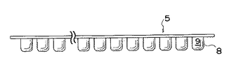
図3及び図4は、それぞれプレス加工によって袋状部8が形成された第2の可撓性フィルム5を示す断面図及び平面図である。
【0033】
次に、第2の可撓性フィルム5の袋状部8にて規定されるセル9内に、電気泳動粒子10及び液体分散媒11が注入される。注入の方法は、特に限定されないが、袋状部8が下方となるようにして第2の可撓性フィルム5を略水平に支持しつつ、第2の可撓性フィルム5上に電気泳動粒子10が混入された液体分散媒11を滴下するか、容器内に満たされた電気泳動粒子10及び液体分散媒11内に第2の可撓性フィルム5を浸漬すればよい。
【0034】
このようにして、第2の可撓性フィルム5の各セル9内に電気泳動粒子10及び液体分散媒11を満たした後、第2の可撓性フィルム5の上方(袋状部8が形成された側と反対側)から第1の可撓性フィルム4を被せる。次に、この状態で第1の可撓性フィルム4及び第2の可撓性フィルム5の接触部を加熱し、これらの接触部分を熱圧着する。これにより、第2の可撓性フィルム5の各セル9は第1の可撓性フィルム4によって閉塞され、各セル9内の電気泳動粒子10及び液体分散媒11は密封される。以上により、第1の可撓性フィルム4及び第2の可撓性フィルム5からなる電気泳動層が完成する。
【0035】
次に、基板2を用意し、基板2上に下層電極3を形成して下面パネルを製造するとともに、保護フィルム7を用意し、保護フィルム7上に上層電極6を形成して上面パネルを製造する。
【0036】
次に、第1の可撓性フィルム4及び第2の可撓性フィルム5からなる電気泳動層を、基板2及び下層電極3からなる下面パネルと上層電極6及び保護フィルム7からなる上面パネルによって挟持する。このとき、第1の可撓性フィルム4及び第2の可撓性フィルム5からなる電気泳動層には所定の圧力、例えば105〜106Paをかけるとともに、減圧状態とする。これにより、各セル9は押しつぶされて変形し、隣り合う袋状部8同士は実質的に密着状態となる。つまり、基板2及び下層電極3からなる下面パネルと上層電極6及び保護フィルム7からなる上面パネルとの間は、実質的に隙間なくセル9によって満たされることになる。
【0037】
次に、第1の可撓性フィルム4及び第2の可撓性フィルム5からなる電気泳動層の減圧状態を維持しつつ、基板2及び下層電極3からなる下面パネルと上層電極6及び保護フィルム7からなる上面パネルとをシール材(図示せず)によって密封し、これによって図1に示される電気泳動表示装置1が完成する。
【0038】
尚、第1の可撓性フィルム4及び第2の可撓性フィルム5からなる電気泳動層を上面パネル及び下面パネルにて挟持する際、第2の可撓性フィルム5の袋状部8の外側に、バインダを塗布することが好ましい。このように、第2の可撓性フィルム5の袋状部8の外側にバインダを塗布すると、第1の可撓性フィルム4及び第2の可撓性フィルム5からなる電気泳動層に圧力が印加され、且つ、減圧状態とされることによって隣り合う袋状部8同士が密着状態となった際に密着状態となった袋状部8同士が接着され、これにより各セル9の強度が高くなる。したがって、電気泳動表示装置1が完成した後、例えば実使用状態において電気泳動表示装置1が大きく曲げられたり強く押し付けられたりして、セル9に対し強い外力が加わった場合にも、袋状部8が破損し、セル9内に封入された電気泳動粒子10及び液体分散媒11がセル9外へ流出する危険性が低くなる。
【0039】
このように、本実施態様にかかる電気泳動表示装置1の製造方法によれば、可撓性を有する樹脂フィルムに対してプレス加工を行って袋状部8を有する第2の可撓性フィルム5を形成し、かかる袋状部8により規定されるセル9内に電気泳動粒子10及び液体分散媒11を満たした後、第1の可撓性フィルム4を熱圧着することによってセル9を閉塞しているので、非常に簡単な方法によりセル構造を有する電気泳動表示装置1を製造することが可能となる。
【0040】
また、上面パネルと下面パネルとの間に、第1の可撓性フィルム4及び第2の可撓性フィルム5からなる電気泳動層を挟持する際、当該電気泳動層に所定の圧力を加えるとともに減圧状態としているので、各セル9は押しつぶされて変形し、下面パネルと上面パネルとの間は、実質的に隙間なくセル9によって満たされる。これにより、セル9間に隙間のない電気泳動表示装置1を製造することが可能となる。
【0041】
本発明は、以上の実施態様に限定されることなく、特許請求の範囲に記載された発明の範囲内で種々の変更が可能であり、それらも本発明の範囲内に包含されるものであることはいうまでもない。
【0042】
例えば、上記実施態様にかかる電気泳動表示装置1では、袋状部8を有する第2の可撓性フィルム5を表示面側に配置し、第1の可撓性フィルム4を表示面とは反対側に配置しているが、第1の可撓性フィルム4及び第2の可撓性フィルム5の配置順としてはこれに限定されず、第1の可撓性フィルム4を表示面側に配置し、袋状部8を有する第2の可撓性フィルム5を表示面とは反対側に配置してもよい。
【0043】
また、上記実施態様にかかる電気泳動表示装置1では、第1の可撓性フィルム4と第2の可撓性フィルム5に同じ材料を用いているが、これらを同じ材料とする必要はなく、互いに異なる材料を用いてもよい。
【0044】
【発明の効果】
以上説明したように、本発明によれば、可撓性を持つとともに軽量な電気泳動表示装置及びこのような電気泳動表示装置を簡易に製造することができる方法を提供することが可能となる。
【図面の簡単な説明】
【図1】図1は、本発明の好ましい実施態様にかかる電気泳動表示装置1を示す断面図である。
【図2】図2は、第2の可撓性フィルム5の製造方法を示す図である。
【図3】図3は、プレス加工によって袋状部8が形成された第2の可撓性フィルム5を示す断面図である。
【図4】図4は、プレス加工によって袋状部8が形成された第2の可撓性フィルム5を示す平面図である。
【符号の説明】
1 電気泳動表示装置
2 基板
3 下層電極
4 第1の可撓性フィルム
5 第2の可撓性フィルム
6 上層電極
7 保護フィルム
8 袋状部
9 セル
10 電気泳動粒子
11 液体分散媒
12、13 金型[0001]
[Industrial application fields]
The present invention relates to an electrophoretic display device and a manufacturing method thereof, and more particularly to a flexible and lightweight electrophoretic display device and a method capable of easily manufacturing such an electrophoretic display device.
[0002]
[Prior art]
Conventionally, an electrophoretic display panel using an electrophoretic phenomenon is known. In the electrophoretic display panel, electrophoretic particles having a positive or negative charge are enclosed, and by applying an electric field to the electrophoretic particles, the electrophoretic display panel collects them on the display surface side of the electrophoretic display panel, Alternatively, a desired figure or the like can be displayed by moving away from the display surface side of the electrophoretic display panel.
[0003]
Known electrophoretic particles used in the electrophoretic display panel include titanium oxide, carbon black, bitumen, and phthalocyanine green. Electrophoretic particles made of such materials are mixed in a liquid dispersion medium such as alcohol solvents, esters, aliphatic hydrocarbons, alicyclic hydrocarbons, aromatic hydrocarbons, halogenated hydrocarbons, and the like. An electrophoretic display panel is configured by being sandwiched by the lower panel.
[0004]
However, if the liquid dispersion medium in which the electrophoretic particles are mixed is simply sandwiched between the upper panel and the lower panel, the electrophoretic particles are aggregated and display unevenness occurs. For this reason, in a conventional electrophoretic display panel, a lattice-like spacer is interposed between the upper panel and the lower panel, and the liquid dispersion medium mixed with the electrophoretic particles is confined in each cell partitioned by the spacer. As a result, aggregation of the electrophoretic particles is prevented and display unevenness is prevented. Further, as another method for preventing the occurrence of display unevenness due to aggregation of electrophoretic particles, a method using a microcapsule and confining a liquid dispersion medium in which the electrophoretic particles are mixed in the microcapsule is known. (See JP-A-1-86116). According to this method, since the microcapsules themselves do not substantially move, the occurrence of display unevenness can be prevented as in the case of using a lattice spacer.
[0005]
Thus, conventionally, a grid-like spacer is interposed between the upper panel and the lower panel, and the liquid dispersion medium in which the electrophoretic particles are mixed in each cell partitioned by the spacer is used, or a microcapsule is used. By confining the liquid dispersion medium in which the electrophoretic particles are mixed in the microcapsule, the electrophoretic particles are prevented from agglomerating and display unevenness is prevented.
[0006]
[Problems to be solved by the invention]
However, when a lattice-like spacer is interposed between the upper panel and the lower panel, the following problem occurs. In other words, in order to sufficiently prevent the electrophoretic particles from moving from each cell partitioned by the spacer to other cells, it is necessary to increase the airtightness of each cell partitioned by the spacer. Sufficient mechanical strength is required. When a spacer having a sufficient mechanical strength is interposed between the upper panel and the lower panel, a problem arises that the flexibility of the electrophoretic display panel is lost. In addition, since a spacer having sufficient mechanical strength is relatively heavy, there is a problem that the weight of the electrophoretic display panel is increased when such a spacer is interposed. Further, when a lattice-like spacer is interposed between the upper panel and the lower panel, the manufacturing process of the electrophoretic display panel becomes complicated, and there is a problem that the manufacturing cost increases.
[0007]
On the other hand, when microcapsules are used, there is no problem that the flexibility of the electrophoretic display panel is lost or the weight of the electrophoretic display panel is increased, but it is difficult to manufacture the microcapsules themselves. This raises the problem of increasing the manufacturing cost. Also, since the shape of the microcapsule is substantially spherical, the contact area between the display surface of the electrophoretic display panel and the microcapsule is very small. As a result, the electrophoretic particles enclosed in the microcapsule move. There is also a problem that there is little change in brightness due to, and the contrast is low.
[0008]
Therefore, a flexible and lightweight electrophoretic display panel and a method capable of easily manufacturing such an electrophoretic display panel have been desired.
[0009]
Accordingly, an object of the present invention is to provide an electrophoretic display device that is flexible and lightweight.
[0010]
Another object of the present invention is to provide a method capable of easily manufacturing a flexible and lightweight electrophoretic display device.
[0011]
[Means for Solving the Problems]
An object of the present invention includes an upper panel, a lower panel, and an electrophoretic layer sandwiched between the upper panel and the lower panel, the electrophoretic layer including a first flexible film, and the first A second flexible film having a plurality of bag-like portions closed by one flexible film, and at least electrophoretic particles are enclosed in the internal space of the closed bag-like portion. This is achieved by an electrophoretic display device.
[0012]
According to the present invention, the electrophoretic layer includes a first flexible film and a second flexible film having a plurality of bag-like portions closed by the first flexible film, Since the electrophoretic particles are sealed in the inner space of the bag-shaped portion, the cell structure can be realized without using a spacer. Thereby, aggregation of the electrophoretic particles is prevented and display unevenness is prevented. In addition, according to the present invention, since the bag-like portion that separates the cells is made of a flexible film, the flexibility of the electrophoretic display device itself is not impaired, and the weight of the electrophoretic display device is reduced. The increase can be minimized.
[0013]
In a preferred embodiment of the present invention, an electrode layer is formed on at least one of the upper panel and the lower panel.
[0014]
In a further preferred embodiment of the present invention, the second flexible film is made of at least one material selected from the group consisting of polyethylene, polypropylene, urethane, acrylic, polyester, fluororesin, nylon, and polyvinyl chloride. Composed.
[0015]
The object of the present invention is also to provide a first step of forming a plurality of bag-like portions on a flexible film, a second step of introducing at least electrophoretic particles into the formed bag-like portion, and the bag. A third step of forming an electrophoretic layer by closing the shaped part and sealing the introduced electrophoretic particles, and a fourth step of sandwiching the electrophoretic layer between the upper panel and the lower panel. This is achieved by a method for manufacturing an electrophoretic display device.
[0016]
According to the present invention, since the electrophoretic particles are introduced into a plurality of bag-like portions formed on the flexible film and closed, the cells for sealing the electrophoretic particles are formed. An electrophoretic display device having a cell structure can be manufactured by a simple method. Therefore, the manufacturing cost of the electrophoretic display device can be kept low.
[0017]
In a preferred embodiment of the present invention, the first step is performed by pressing the flexible film.
[0018]
In a further preferred embodiment of the present invention, the third step is performed by adhering another flexible film to the flexible film in which the electrophoretic particles are introduced into the bag-like portion.
[0019]
In a further preferred embodiment of the present invention, the fourth step is performed under reduced pressure.
[0020]
According to a further preferred embodiment of the present invention, since the fourth step of sandwiching the electrophoretic layer between the upper panel and the lower panel is performed under reduced pressure, each cell defined by the bag-like portion is crushed and deformed. In addition, the space between the lower surface panel and the upper surface panel can be filled with cells substantially without a gap. This makes it possible to manufacture an electrophoretic display device with no gap between cells.
[0021]
In a further preferred embodiment of the present invention, the method further comprises a step of applying a binder to the outside of the plurality of bag-like portions of the flexible film.
[0022]
According to a further preferred embodiment of the present invention, since the binder is applied to the outside of the plurality of bag-like portions of the flexible film, the bag-like portions are bonded to each other, thereby increasing the strength of each cell. Therefore, after the electrophoretic display device is completed, even when the electrophoretic display device is greatly bent or strongly pressed in an actual use state and a strong external force is applied to the cell, the bag-like portion is damaged. The risk of the electrophoretic particles enclosed in the cell flowing out of the cell is reduced.
[0023]
Preferred Embodiment of the Invention
Hereinafter, preferred embodiments of the present invention will be described in detail with reference to the accompanying drawings.
[0024]
FIG. 1 is a cross-sectional view showing an electrophoretic display device 1 according to a preferred embodiment of the present invention.
[0025]
As shown in FIG. 1, an electrophoretic display device 1 according to this embodiment includes a
[0026]
The
[0027]
In the electrophoretic display device 1 having such a configuration, for example, when the
[0028]
As described above, the electrophoretic display device 1 according to the present embodiment includes a large number of
[0029]
Next, a method for manufacturing the electrophoretic display device 1 will be described.
[0030]
FIG. 2 is a diagram illustrating a method for manufacturing the second
[0031]
As shown in FIG. 2, first, a resin film such as polyethylene, polypropylene, urethane, acrylic, polyester, fluororesin, nylon, and polyvinyl chloride, which is a material of the second
[0032]
3 and 4 are a cross-sectional view and a plan view showing the second
[0033]
Next, the
[0034]
In this way, after each
[0035]
Next, the
[0036]
Next, the electrophoretic layer composed of the first
[0037]
Next, while maintaining the reduced pressure state of the electrophoretic layer comprising the first
[0038]
When the electrophoretic layer composed of the first
[0039]
Thus, according to the manufacturing method of the electrophoretic display device 1 according to the present embodiment, the second
[0040]
Further, when an electrophoretic layer composed of the first
[0041]
The present invention is not limited to the above-described embodiments, and various modifications are possible within the scope of the invention described in the claims, and these are also included in the scope of the present invention. Needless to say.
[0042]
For example, in the electrophoretic display device 1 according to the above embodiment, the second
[0043]
Moreover, in the electrophoretic display device 1 according to the above embodiment, the same material is used for the first
[0044]
【The invention's effect】
As described above, according to the present invention, it is possible to provide a flexible and lightweight electrophoretic display device and a method capable of easily manufacturing such an electrophoretic display device.
[Brief description of the drawings]
FIG. 1 is a cross-sectional view showing an electrophoretic display device 1 according to a preferred embodiment of the present invention.
FIG. 2 is a diagram showing a method for manufacturing the second
FIG. 3 is a cross-sectional view showing a second
FIG. 4 is a plan view showing a second
[Explanation of symbols]
DESCRIPTION OF SYMBOLS 1
Claims (8)
Priority Applications (1)
| Application Number | Priority Date | Filing Date | Title |
|---|---|---|---|
| JP2000205200A JP4399962B2 (en) | 2000-07-06 | 2000-07-06 | Electrophoretic display device and manufacturing method thereof |
Applications Claiming Priority (1)
| Application Number | Priority Date | Filing Date | Title |
|---|---|---|---|
| JP2000205200A JP4399962B2 (en) | 2000-07-06 | 2000-07-06 | Electrophoretic display device and manufacturing method thereof |
Publications (2)
| Publication Number | Publication Date |
|---|---|
| JP2002023202A JP2002023202A (en) | 2002-01-23 |
| JP4399962B2 true JP4399962B2 (en) | 2010-01-20 |
Family
ID=18702330
Family Applications (1)
| Application Number | Title | Priority Date | Filing Date |
|---|---|---|---|
| JP2000205200A Expired - Fee Related JP4399962B2 (en) | 2000-07-06 | 2000-07-06 | Electrophoretic display device and manufacturing method thereof |
Country Status (1)
| Country | Link |
|---|---|
| JP (1) | JP4399962B2 (en) |
Families Citing this family (4)
| Publication number | Priority date | Publication date | Assignee | Title |
|---|---|---|---|---|
| JP2003216111A (en) * | 2002-01-28 | 2003-07-30 | Sharp Corp | Device and system of display |
| US6885146B2 (en) * | 2002-03-14 | 2005-04-26 | Semiconductor Energy Laboratory Co., Ltd. | Display device comprising substrates, contrast medium and barrier layers between contrast medium and each of substrates |
| US6940634B2 (en) | 2003-03-27 | 2005-09-06 | Canon Kabushiki Kaisha | Electrophoretic display device |
| JP2007179079A (en) * | 2007-03-29 | 2007-07-12 | Hatsumeiya:Kk | Air bubble sheet type electronic paper |
-
2000
- 2000-07-06 JP JP2000205200A patent/JP4399962B2/en not_active Expired - Fee Related
Also Published As
| Publication number | Publication date |
|---|---|
| JP2002023202A (en) | 2002-01-23 |
Similar Documents
| Publication | Publication Date | Title |
|---|---|---|
| JP4059034B2 (en) | Electrophoresis device, electronic apparatus, and method of manufacturing the electrophoresis device | |
| JP4366059B2 (en) | Electrophoretic display device | |
| US6130773A (en) | Nonemissive displays and piezoelectric power supplies therefor | |
| US7622148B2 (en) | Method for manufacturing electrophoretic display element | |
| JP4883526B2 (en) | Electrophoretic display device and manufacturing method thereof | |
| KR20070079581A (en) | Electrophoretic display device and electronic apparatus | |
| JP4399962B2 (en) | Electrophoretic display device and manufacturing method thereof | |
| US8217869B2 (en) | Flexible display system | |
| EP1677141A1 (en) | Electrophoretic display device and method of manufacture | |
| WO2006040928A1 (en) | Display medium and process for producing the same | |
| JP2002148663A (en) | Display device and method of manufacturing the same | |
| JP4508322B2 (en) | Display device | |
| JP4048679B2 (en) | Electrophoretic display device and manufacturing method thereof | |
| US20050146776A1 (en) | Method of manufacturing electrophoretic display | |
| JP4868560B2 (en) | Display device and manufacturing method thereof | |
| US8248362B1 (en) | Method of manufacturing an electrophoretic display | |
| US8629833B1 (en) | Single particle electrophoretic display and method of manufacturing same | |
| KR100693744B1 (en) | Electrical Paper Display Having high Contrast and Manufacturing Method Thereof | |
| US8519944B2 (en) | Dual particle electrophoretic display and method of manufacturing same | |
| KR101294342B1 (en) | Reflective display device | |
| CN114265256B (en) | Manufacturing method of electronic paper display equipment | |
| JP2004157237A (en) | Display | |
| KR101228189B1 (en) | Manufacturing Process of Electronic Paper Display Device and Electronic Paper Display Device Using The Same | |
| JP4433670B2 (en) | Image display medium | |
| JP2004301947A (en) | Display device |
Legal Events
| Date | Code | Title | Description |
|---|---|---|---|
| A621 | Written request for application examination |
Free format text: JAPANESE INTERMEDIATE CODE: A621 Effective date: 20051128 |
|
| TRDD | Decision of grant or rejection written | ||
| A01 | Written decision to grant a patent or to grant a registration (utility model) |
Free format text: JAPANESE INTERMEDIATE CODE: A01 Effective date: 20091006 |
|
| A01 | Written decision to grant a patent or to grant a registration (utility model) |
Free format text: JAPANESE INTERMEDIATE CODE: A01 |
|
| R150 | Certificate of patent or registration of utility model |
Ref document number: 4399962 Country of ref document: JP Free format text: JAPANESE INTERMEDIATE CODE: R150 Free format text: JAPANESE INTERMEDIATE CODE: R150 |
|
| A61 | First payment of annual fees (during grant procedure) |
Free format text: JAPANESE INTERMEDIATE CODE: A61 Effective date: 20091019 |
|
| FPAY | Renewal fee payment (event date is renewal date of database) |
Free format text: PAYMENT UNTIL: 20121106 Year of fee payment: 3 |
|
| FPAY | Renewal fee payment (event date is renewal date of database) |
Free format text: PAYMENT UNTIL: 20121106 Year of fee payment: 3 |
|
| FPAY | Renewal fee payment (event date is renewal date of database) |
Free format text: PAYMENT UNTIL: 20131106 Year of fee payment: 4 |
|
| LAPS | Cancellation because of no payment of annual fees |