JP4382502B2 - Liquid crystal display - Google Patents
Liquid crystal display Download PDFInfo
- Publication number
- JP4382502B2 JP4382502B2 JP2004000526A JP2004000526A JP4382502B2 JP 4382502 B2 JP4382502 B2 JP 4382502B2 JP 2004000526 A JP2004000526 A JP 2004000526A JP 2004000526 A JP2004000526 A JP 2004000526A JP 4382502 B2 JP4382502 B2 JP 4382502B2
- Authority
- JP
- Japan
- Prior art keywords
- liquid crystal
- degrees
- retardation
- layer
- axis
- Prior art date
- Legal status (The legal status is an assumption and is not a legal conclusion. Google has not performed a legal analysis and makes no representation as to the accuracy of the status listed.)
- Expired - Fee Related
Links
Images


Classifications
-
- G—PHYSICS
- G02—OPTICS
- G02F—OPTICAL DEVICES OR ARRANGEMENTS FOR THE CONTROL OF LIGHT BY MODIFICATION OF THE OPTICAL PROPERTIES OF THE MEDIA OF THE ELEMENTS INVOLVED THEREIN; NON-LINEAR OPTICS; FREQUENCY-CHANGING OF LIGHT; OPTICAL LOGIC ELEMENTS; OPTICAL ANALOGUE/DIGITAL CONVERTERS
- G02F1/00—Devices or arrangements for the control of the intensity, colour, phase, polarisation or direction of light arriving from an independent light source, e.g. switching, gating or modulating; Non-linear optics
- G02F1/01—Devices or arrangements for the control of the intensity, colour, phase, polarisation or direction of light arriving from an independent light source, e.g. switching, gating or modulating; Non-linear optics for the control of the intensity, phase, polarisation or colour
- G02F1/13—Devices or arrangements for the control of the intensity, colour, phase, polarisation or direction of light arriving from an independent light source, e.g. switching, gating or modulating; Non-linear optics for the control of the intensity, phase, polarisation or colour based on liquid crystals, e.g. single liquid crystal display cells
- G02F1/137—Devices or arrangements for the control of the intensity, colour, phase, polarisation or direction of light arriving from an independent light source, e.g. switching, gating or modulating; Non-linear optics for the control of the intensity, phase, polarisation or colour based on liquid crystals, e.g. single liquid crystal display cells characterised by the electro-optical or magneto-optical effect, e.g. field-induced phase transition, orientation effect, guest-host interaction or dynamic scattering
- G02F1/139—Devices or arrangements for the control of the intensity, colour, phase, polarisation or direction of light arriving from an independent light source, e.g. switching, gating or modulating; Non-linear optics for the control of the intensity, phase, polarisation or colour based on liquid crystals, e.g. single liquid crystal display cells characterised by the electro-optical or magneto-optical effect, e.g. field-induced phase transition, orientation effect, guest-host interaction or dynamic scattering based on orientation effects in which the liquid crystal remains transparent
- G02F1/1393—Devices or arrangements for the control of the intensity, colour, phase, polarisation or direction of light arriving from an independent light source, e.g. switching, gating or modulating; Non-linear optics for the control of the intensity, phase, polarisation or colour based on liquid crystals, e.g. single liquid crystal display cells characterised by the electro-optical or magneto-optical effect, e.g. field-induced phase transition, orientation effect, guest-host interaction or dynamic scattering based on orientation effects in which the liquid crystal remains transparent the birefringence of the liquid crystal being electrically controlled, e.g. ECB-, DAP-, HAN-, PI-LC cells
-
- G—PHYSICS
- G02—OPTICS
- G02F—OPTICAL DEVICES OR ARRANGEMENTS FOR THE CONTROL OF LIGHT BY MODIFICATION OF THE OPTICAL PROPERTIES OF THE MEDIA OF THE ELEMENTS INVOLVED THEREIN; NON-LINEAR OPTICS; FREQUENCY-CHANGING OF LIGHT; OPTICAL LOGIC ELEMENTS; OPTICAL ANALOGUE/DIGITAL CONVERTERS
- G02F1/00—Devices or arrangements for the control of the intensity, colour, phase, polarisation or direction of light arriving from an independent light source, e.g. switching, gating or modulating; Non-linear optics
- G02F1/01—Devices or arrangements for the control of the intensity, colour, phase, polarisation or direction of light arriving from an independent light source, e.g. switching, gating or modulating; Non-linear optics for the control of the intensity, phase, polarisation or colour
- G02F1/13—Devices or arrangements for the control of the intensity, colour, phase, polarisation or direction of light arriving from an independent light source, e.g. switching, gating or modulating; Non-linear optics for the control of the intensity, phase, polarisation or colour based on liquid crystals, e.g. single liquid crystal display cells
- G02F1/133—Constructional arrangements; Operation of liquid crystal cells; Circuit arrangements
- G02F1/1333—Constructional arrangements; Manufacturing methods
- G02F1/1337—Surface-induced orientation of the liquid crystal molecules, e.g. by alignment layers
-
- G—PHYSICS
- G02—OPTICS
- G02F—OPTICAL DEVICES OR ARRANGEMENTS FOR THE CONTROL OF LIGHT BY MODIFICATION OF THE OPTICAL PROPERTIES OF THE MEDIA OF THE ELEMENTS INVOLVED THEREIN; NON-LINEAR OPTICS; FREQUENCY-CHANGING OF LIGHT; OPTICAL LOGIC ELEMENTS; OPTICAL ANALOGUE/DIGITAL CONVERTERS
- G02F1/00—Devices or arrangements for the control of the intensity, colour, phase, polarisation or direction of light arriving from an independent light source, e.g. switching, gating or modulating; Non-linear optics
- G02F1/01—Devices or arrangements for the control of the intensity, colour, phase, polarisation or direction of light arriving from an independent light source, e.g. switching, gating or modulating; Non-linear optics for the control of the intensity, phase, polarisation or colour
- G02F1/13—Devices or arrangements for the control of the intensity, colour, phase, polarisation or direction of light arriving from an independent light source, e.g. switching, gating or modulating; Non-linear optics for the control of the intensity, phase, polarisation or colour based on liquid crystals, e.g. single liquid crystal display cells
- G02F1/133—Constructional arrangements; Operation of liquid crystal cells; Circuit arrangements
- G02F1/1333—Constructional arrangements; Manufacturing methods
- G02F1/1335—Structural association of cells with optical devices, e.g. polarisers or reflectors
- G02F1/13363—Birefringent elements, e.g. for optical compensation
- G02F1/133638—Waveplates, i.e. plates with a retardation value of lambda/n
-
- G—PHYSICS
- G02—OPTICS
- G02F—OPTICAL DEVICES OR ARRANGEMENTS FOR THE CONTROL OF LIGHT BY MODIFICATION OF THE OPTICAL PROPERTIES OF THE MEDIA OF THE ELEMENTS INVOLVED THEREIN; NON-LINEAR OPTICS; FREQUENCY-CHANGING OF LIGHT; OPTICAL LOGIC ELEMENTS; OPTICAL ANALOGUE/DIGITAL CONVERTERS
- G02F2413/00—Indexing scheme related to G02F1/13363, i.e. to birefringent elements, e.g. for optical compensation, characterised by the number, position, orientation or value of the compensation plates
- G02F2413/14—Negative birefingence
Description
本発明は、液晶表示装置に関する。 The present invention relates to a liquid crystal display device.
特許文献1には、垂直配向型液晶セルと、該液晶セルの両側に配置された第1及び第2の偏光板と、液晶セルと第1の偏光板との間に配置された第1のλ/4板と、液晶セルと第2の偏光板との間に配置された第2のλ/4板と、を備えた液晶表示装置が開示されている。ここで、λは光の波長を表す。特許文献1の技術では、斜め方向から見たときの視角特性が改善される。
また、外光下でも視認性の良いディスプレイの開発が進められている。例えば、反射型及び透過型を兼ね備え、かつ黒表示時の特性を改善した液晶表示装置が特許文献2に開示されている。特許文献2の液晶表示装置は、主に、その垂直配向型液晶セルが、透過部と反射部とを有する点で上記特許文献1と異なる技術である。ここで、垂直配向液晶は電圧無印加時に黒表示を電圧印加時に白表示を行うノーマリーブラックモードで用いられる。ノーマリーブラックの垂直配向液晶を用いることにより、TNモードやSTNモードを用いる場合よりもコントラストを改善している。
In addition, the development of a display with high visibility even under external light is underway. For example,
また特許文献3には、上記特許文献1の液晶表示装置の構成に加え、第1のλ/4板と液晶セルとの間、並びに、第2のλ/4板と液晶セルとの間、にそれぞれ配された負の1軸光学補償層を備えている。特許文献3の技術は、λ/4板を用いた垂直配向型液晶表示装置における黒表示の視角特性を改善する方法に関する。
Further, in
また、特許文献3の技術とマルチドメイン(分割配向型)垂直配向液晶表示装置を組み合わせた技術として、特許文献4の技術がある。なお、分割配向とは、1画素の中に配向状態が相互に異なる複数のドメイン(領域)を形成すること(或いは形成されている状態)をいう。
ところで、上記の技術のうち、特許文献1の液晶表示装置では、コントラストの対称性が悪いという問題があり、また、特許文献2の液晶表示装置では、コントラストの対称性は改善されるものの、基板法線方向から視角を変えた場合、光漏れが発生するという問題がある。
By the way, among the above techniques, the liquid crystal display device disclosed in
また、特許文献3、4のように垂直配向液晶セルとλ/4板、負の1軸の光学補償層を組み合わせた液晶表示装置では、良好な視角特性が得られないことがあるという問題がある。
In addition, as in
なお、特許文献4の段落0068には「コントラストが最も保たれる方位は上下左右から反時計回りに約30度回転した」例が開示されている。更に、この改善例として、同特許文献4の段落0072に「偏光板20,22の角度を最適化して、コントラストが最大となる視角方位を上下左右方向とした」例が開示されている。しかしながら、特許文献4には、コントラストが最も保たれる方位が回転した理由、液晶層のリタデーションと補償層のリタデーションと偏光板の配置角度の関係が明示されていない。
In addition, paragraph 0068 of
本発明は、上記のような問題点を解決するためになされたもので、黒表示時の45度、135度、225度、315度方向の光漏れを抑え、かつ対称な視角特性を持つ液晶表示装置を提供することを目的とする。 The present invention has been made to solve the above-described problems, and suppresses light leakage in the directions of 45 degrees, 135 degrees, 225 degrees, and 315 degrees during black display, and has a symmetrical viewing angle characteristic. An object is to provide a display device.
始めに、垂直配向液晶セル、λ/4板(位相差板)及び負の1軸の光学補償層(負の1軸の位相差を有する光学層)を組み合わせた液晶表示装置(特許文献3、4)の視角特性が必ずしも対称にならない理由を説明しておく。
First, a liquid crystal display device that combines a vertical alignment liquid crystal cell, a λ / 4 plate (retardation plate), and a negative uniaxial optical compensation layer (an optical layer having a negative uniaxial retardation) (
先ず、図1に示すようにλ/4板を有しない構成の液晶表示装置100の視角特性、についてシミュレーションを行った結果を説明する。
First, the results of a simulation performed on the viewing angle characteristics of the liquid
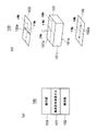
図1は、液晶表示装置100を示す模式図であり、このうち(a)は正面断面図、(b)は分解斜視図である。
FIG. 1 is a schematic view showing a liquid
図1に示すように、液晶表示装置100は、垂直配向液晶セル101と、この垂直配向液晶セル101の表裏両側にそれぞれ配置された第1及び第2の偏光板(偏光層)102、103と、を備える。
As shown in FIG. 1, a liquid
このうち垂直配向液晶セル101は、各々電極(図示略)を有する一対の基板101a、101bと、これら一対の基板101a、101bに挟持された液晶層101cと、からなる。
Among these, the vertical alignment
ここで、液晶表示装置100の表示面(基板101a及び基板101bの板面方向に等しい)に相対したときの横方向にx軸(図1(b))を取り、縦方向にy軸を取ることとし、各構成要素の配置角度はx軸に対する角度(方位角)で表すことにする。なお、x軸及びy軸は、液晶層101cにおける配向分割の対称軸でもある。
Here, the x-axis (FIG. 1 (b)) is taken in the horizontal direction and the y-axis is taken in the vertical direction when facing the display surface of the liquid crystal display device 100 (equal to the plate surface direction of the
また、基板101a(或いは基板101b)より観察者側に向かう法線方向にz軸を取ることとし、極角はz軸に対する角度とする。
Further, the z axis is taken in the normal direction from the
図1に示す液晶表示装置100において、第1の偏光板102は、その吸収軸102a(図1(b))が方位角0度の方向となるように配置され、該第1の偏光板102の上に垂直配向液晶セル101が配置されている。更に、垂直配向液晶セル101の上には、第2の偏光板103が、その吸収軸103a(図1(b))が方位角90度の方向となるように配置されている。従って、第1及び第2の偏光板102、103により直交偏光板が構成されている。
In the liquid
ここで、図2は電圧無印加時の液晶配向の状態を示す模式図であり、図3は電圧印加時の液晶配向の状態を示す模式図である。図2及び図3の各図において、(a)は平面図、(b)は正面断面図である。 Here, FIG. 2 is a schematic diagram showing a liquid crystal alignment state when no voltage is applied, and FIG. 3 is a schematic diagram showing a liquid crystal alignment state when a voltage is applied. 2 and 3, (a) is a plan view and (b) is a front sectional view.
垂直配向液晶セル101の液晶層101cは、負の誘電率異方性を持つ液晶が充填されている。
The
液晶層101cの液晶(液晶分子E)は、電圧無印加時には図2に示すように基板101a、101bに対して垂直配向する。
The liquid crystal (liquid crystal molecule E) in the
他方、電圧印加時には図3に示すように、4分割された各領域において相互に同量の液晶(液晶分子E)が、方位角45度、135度、225度及び315度の4つの方向に(各領域の反対側に向けて)それぞれ倒れる。つまり、方位角45度方向に位置する液晶は方位角225度方向に倒れ、方位角135度方向に位置する液晶は方位角315度方向に倒れ、方位角225度方向に位置する液晶は方位角45度方向に倒れ、方位角315度方向に位置する液晶は方位角135度方向に倒れる。 On the other hand, when a voltage is applied, as shown in FIG. 3, the same amount of liquid crystal (liquid crystal molecule E) is divided into four directions of azimuth angles of 45 degrees, 135 degrees, 225 degrees, and 315 degrees as shown in FIG. Each falls down (towards the opposite side of each area). That is, the liquid crystal located in the azimuth angle of 45 degrees is tilted in the azimuth angle of 225 degrees, the liquid crystal located in the azimuth angle of 135 degrees is tilted in the azimuth angle of 315 degrees, and the liquid crystal located in the azimuth angle of 225 degrees is The liquid crystal tilted in the 45 degree direction and the liquid crystal located in the azimuth angle of 315 degrees direction falls in the azimuth angle direction of 135 degrees.
すなわち、液晶表示装置100の垂直配向液晶セル101としては、このような4分割配向のものを用いた。
That is, as the vertically aligned
また、垂直配向液晶セル101は、電圧無印加時には黒表示を行い、電圧印加時に白表示を行うノーマリーブラックモードである。また、液晶のΔn(複屈折率)=0.0741、セルギャップ(液晶層101cの厚み)を4.5μmとした。
The vertical alignment
このような構成の液晶表示装置100における電圧無印加時(黒表示時)の透過率分布を図4に、電圧印加時(白表示時)の透過率分布を図5に、それぞれ示し、電圧無印加時と電圧印加時を比較した等コントラスト曲線を図6に示す。
FIG. 4 shows the transmittance distribution when no voltage is applied (black display) and FIG. 5 shows the transmittance distribution when voltage is applied (white display) in the liquid
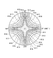
ここで、図4、図5、図6の見方を説明する。 Here, how to view FIGS. 4, 5, and 6 will be described.
各図に示される同心円の中心は極角0度の方向を表し、同心円の中心から遠ざかるにつれて極角が増し、最内周の円は極角が22.5度、その外側の円は極角が45度、更にその外側の円は極角が67.5度、最外周の円は極角が90度を表す。また、各図の0度−180度方向は横方向(x軸方向)に対応し、90度−270度方向は縦方向(y軸方向)に対応する。そして、図4及び図5は、ある極角、ある方位角から見たときの透過率を調べたもののうち、透過率が等しくなるような点の軌跡を同心円中に書き込んだものである。同様に、図6は、ある極角、ある方位角から見たときのコントラストを調べたもののうち、コントラストが等しくなるような点の軌跡を同心円中に書き込んだものである。
The center of the concentric circles shown in each figure indicates the direction of the
なお、図4及び図5においては、図中に示される領域R1の透過率が最も高く、以下、領域R2、R3、R4、R5、R6、R7、R8、R9の順に次第に透過率が低くなる。また、図6においては、図中に示される領域R11のコントラストが最も高く、以下、領域R12、R13、R14、R15、R16、R17、R18の順に次第にコントラストが低くなる。なお、図6において、領域R16と領域R17との境界線は、コントラスト=10の等コントラスト曲線である。 4 and 5, the transmittance of the region R1 shown in the drawing is the highest, and the transmittance gradually decreases in the order of the regions R2, R3, R4, R5, R6, R7, R8, and R9. . In FIG. 6, the contrast of the region R11 shown in the drawing is the highest, and the contrast gradually decreases in the order of the regions R12, R13, R14, R15, R16, R17, and R18. In FIG. 6, the boundary line between the region R16 and the region R17 is an isocontrast curve with contrast = 10.
図4に示すように、図1の液晶表示装置100の場合に黒表示時の透過率(以下、単に黒の透過率)が高くなる方向(光漏れする方向)は、方位角45度、135度、225度、315度の方向となっている。なお、白表示時の透過率(以下、単に白の透過率)は、図5に示すように、x軸、y軸において全方向に均一に分布している。また、コントラスト曲線は、図6に示すように、x軸、y軸に関して対称な形をしている。
As shown in FIG. 4, in the case of the liquid
次ぎに、図7に正面断面図(図7(a))及び分解斜視図(図7(b))が示される液晶表示装置110の視角特性についてシミュレーションを行った結果を説明する。なお、図7に示す液晶表示装置110の各構成要素のうち、図1に示す液晶表示装置100と同様の構成要素には同一の符号を付している。
Next, the results of simulation of the viewing angle characteristics of the liquid
図7に示すように、液晶表示装置110は、図1の液晶表示装置100に負の1軸の光学補償層(負の1軸の位相差を有する光学層)112、113を追加した構成となっている。
As shown in FIG. 7, the liquid
すなわち、液晶表示装置110においては、第1の光学補償層112は、垂直配向液晶セル101と第1の偏光板102との間に配置され、第2の光学補償層113は、垂直配向液晶セル101と第2の偏光板103との間に配置されている。なお、図7の液晶表示装置110において、第1及び第2の偏光板102、103の吸収軸102a、103aの方向は、それぞれ図1の液晶表示装置100の場合と同様である。
That is, in the liquid
図7の液晶表示装置110の場合に黒の透過率が高くなる方向は、図1の液晶表示装置100と同様であり、方位角45度、135度、225度、315度の方向から変化しなかった。また、コントラスト曲線もx軸、y軸に関して対称な形を維持したままであった。
In the case of the liquid
また、負の1軸の光学補償層112、113の厚み方向のリタデーションが50nmと100nmとの2種類の場合(つまり、第1及び第2の光学補償層112,113のリタデーションの和が100nmの場合と200nmの場合)について視角特性を調べた。
Further, when the retardation in the thickness direction of the negative uniaxial
図8は、図7の液晶表示装置120において、一対の負の1軸の光学補償層112、113のリタデーションの和を横軸にとり、黒の透過率が最も高くなる方向を縦軸にとったグラフである。
8, in the liquid
図8に示すように、黒の透過率が高くなる方向は、負の1軸の光学補償層112、113の厚み方向のリタデーションの大きさに影響を受けなかった。
As shown in FIG. 8, the direction in which the black transmittance increases was not affected by the thickness of the negative uniaxial
このように、λ/4板を有さず、直交偏光板(第1及び第2の偏光板102、103)、負の1軸の光学補償層(第1及び第2の光学補償層112、113)及び垂直配向液晶セル101を組み合わせた構成では、黒表示時に光漏れする方向は偏光板(第1及び第2の偏光板102、103)の各吸収軸102a、103aに対し45度の方向(つまり、方位角45度、135度、225度及び315度の4方向)である。
In this way, there is no λ / 4 plate, orthogonal polarizing plates (first and second
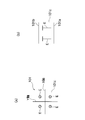
次ぎに、図9に正面断面図(図9(a))及び分解斜視図(図9(b))が示される液晶表示装置120の視角特性についてシミュレーションを行った結果を説明する。なお、図9に示す液晶表示装置120の各構成要素のうち、図1に示す液晶表示装置100と同様の構成要素には同一の符号を付している。
Next, the result of having performed the simulation about the viewing angle characteristic of the liquid
図9に示すように、液晶表示装置120は、垂直配向液晶セル101と、該垂直配向セル101の表裏両側に配された第1及び第2のλ/4板122、123と、更にその両側に配された第1及び第2の偏光板102、103と、を備えている。つまり、液晶表示装置120は、図1の液晶表示装置100にλ/4板122、123を追加した構成となっていて、上記特許文献1の液晶表示装置に相当する。
As shown in FIG. 9, the liquid
液晶表示装置120において、第1及び第2の偏光板102、103は、液晶表示装置100の場合と同様に、それぞれ、その吸収軸102a、103aが0度、90度の方向となるように配置した。
In the liquid
また、第1のλ/4板122は、その遅相軸122aが方位角135度の方向となるように配置され、第2のλ/4板123は、その遅相軸123aが方位角45度の方向となるように配置した。
The first λ / 4
また、第1及び第2のλ/4板122、123の面内のリタデーションは各々138nmとした。
The in-plane retardation of the first and second λ / 4
このような構成の液晶表示装置120における電圧無印加時(黒表示時)の透過率分布を図10に、電圧印加時(白表示時)の透過率分布を図11に、それぞれ示し、電圧無印加時と電圧印加時を比較した等コントラスト曲線を図12に示す。なお、図10〜図12において、符号R1〜R9、並びに、符号R11〜R18は、図4〜図6におけるのと同様である。
In the liquid
図12に示すように、等コントラスト曲線はx軸、y軸に関して非対称となった。 As shown in FIG. 12, the isocontrast curve was asymmetric with respect to the x-axis and the y-axis.
また、図11に示すように、電圧印加時の透過率分布はx軸、y軸に関して対称である。 Further, as shown in FIG. 11, the transmittance distribution at the time of voltage application is symmetric with respect to the x-axis and the y-axis.
また、図10に示すように、電圧無印加時において黒の透過率が高くなる方向は、方位角45度、135度、225度、315度の方向から変化している。 Further, as shown in FIG. 10, the direction in which the black transmittance increases when no voltage is applied changes from the directions of azimuth angles of 45 degrees, 135 degrees, 225 degrees, and 315 degrees.
このように液晶表示装置120における視角特性が非対称となったのは、電圧無印加時において黒の透過率が高くなる方向が、λ/4板の存在により、液晶表示装置100及び液晶表示装置110の場合と比べてずれるためであると考えられる。
As described above, the viewing angle characteristics of the liquid
次ぎに、図13に正面断面図(図13(a))、分解斜視図(図13(b))及び各構成要素の配置角度(図13(c))が示される液晶表示装置130の視角特性についてシミュレーションを行った結果を説明する。なお、図13に示す液晶表示装置130の各構成要素のうち、図7、図9に示す液晶表示装置110、120と同様の構成要素には同一の符号を付している。
Next, FIG. 13 is a front sectional view (FIG. 13A), an exploded perspective view (FIG. 13B), and an arrangement angle of each component (FIG. 13C). The results of simulation of characteristics will be described. Of the components of the liquid
図13に示すように、液晶表示装置130は、図9の液晶表示装置120に負の1軸の光学補償層112、113を追加した構成となっていて、上記特許文献3の液晶表示装置に相当する。
As shown in FIG. 13, the liquid
すなわち、液晶表示装置130においては、第1の光学補償層112は、垂直配向液晶セル101と第1のλ/4板122との間に配置され、第2の光学補償層113は、垂直配向液晶セル101と第2のλ/4板123との間に配置されている。なお、図13の液晶表示装置130において、第1及び第2の偏光板102、103の吸収軸102a、103aの方向は、それぞれ図1の液晶表示装置100の場合と同様であり、第1及び第2のλ/4板122、123の遅相軸122a、123aの方向は、それぞれ図9の液晶表示装置110の場合と同様である。つまり、第1及び第2の偏光板102、103の吸収軸102a、103aの方向は、液晶層101cにおける配向分割の対称軸に一致する。
That is, in the liquid
このような液晶表示装置120において、第1及び第2の光学補償層112、113の厚み方向のリタデーションが25nm、50nm、75nm、100nm、125nm及び150nmの6種類の場合(つまり、第1及び第2の光学補償層112,113のリタデーションの和が50nm、100nm、150nm、200nm、250nm及び300nmの場合)について視角特性を調べた。
In such a liquid
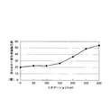
図14は、図13の液晶表示装置130において、一対の負の1軸の光学補償層112、113のリタデーションの和を横軸にとり、黒の透過率が最も高くなる方向を縦軸にとったグラフである。
FIG. 14 shows the sum of the retardations of the pair of negative uniaxial
図14に示すように、液晶表示装置130の場合には、黒の透過率が高くなる方向が方位角45度の方向からずれ、しかも、そのずれ角度が、光学補償層112、113のリタデーションに応じて変化していることがわかる。
As shown in FIG. 14, in the case of the liquid
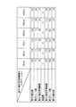
そこで、この角度を相殺するように第1及び第2の偏光板102、103、第1及び第2のλ/4板122、123、第1及び第2の光学補償層112、113の配置角度(単位:度)を図15のように(光学補償層112、113のリタデーションに応じて)設定した。
Therefore, the arrangement angles of the first and second
ここで、図15に示される配置角度は、第1及び第2の偏光板102、103については、その吸収軸102a、103aの方位角を示し、第1及び第2のλ/4板122、123については、その遅相軸122a、123aの方位角を示し、第1及び第2の光学補償層112、113については、遅相軸の方位角を示す。
Here, the arrangement angle shown in FIG. 15 indicates the azimuth angle of the
図16には、第1及び第2の負の1軸の光学補償層112、113の厚み方向のリタデーションが75nm(和は150nm)の場合の結果(等コントラスト曲線)を示す。なお、図16の場合、各構成要素の配置角度は、図15に示すように、第1の偏光板102が19度、第1のλ/4板122が154度、第1の光学補償層112が109度、第2の光学補償層113が19度、第2のλ/4板123が64度、第2の偏光板103が109度である。
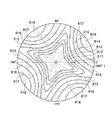
FIG. 16 shows a result (isocontrast curve) in the case where the thickness direction retardation of the first and second negative uniaxial
また、図16並びに以下に説明する図17乃至図19において、符号R11〜R18は、図6におけるのと同様である。 In FIG. 16 and FIGS. 17 to 19 described below, reference numerals R11 to R18 are the same as those in FIG.
図16に示すように、第1及び第2の負の1軸の光学補償層112、113の厚み方向のリタデーションが75nm(和は150nm)の場合に図15に示す設定とすることにより、すなわち、液晶表示装置130の視角特性が対称となるように、第1及び第2の偏光板102、103の吸収軸102a、103aを液晶層101cにおける配向分割の対称軸に対してずらし、それに伴い第1及び第2のλ/4板122、123、第1及び第2の光学補償層112、113の配置角度もずらすことにより、対称な視角特性が得られた。また、45度、135度、225度及び315度の方向でコントラスト>10となる極角方向の範囲が55度となった。
As shown in FIG. 16, when the retardation in the thickness direction of the first and second negative uniaxial
他方、図17には、図16の場合の比較例として、負の1軸の光学補償層112、113の厚み方向のリタデーションは図16の場合と同じであるが、第1及び第2の偏光板102、103と、第1及び第2のλ/4板122、123と、第1及び第2の光学補償板112、113とを従来の配置角度(図13(c))で配置した場合、つまり、第1及び第2の偏光板102、103の吸収軸102a、103aが液晶層101cにおける配向分割の対称軸に一致するように配置した場合の視角特性を示す。この場合、図17に示すように、0度−180度方向、90度−270度方向に関して非対称な視角特性になっている。
On the other hand, in FIG. 17, as a comparative example in the case of FIG. 16, the retardation in the thickness direction of the negative uniaxial
また、図18には、第1及び第2の負の1軸の光学補償層112、113の厚み方向のリタデーションが100nm(和は200nm)の場合の結果を示す。なお、各構成要素の配置角度は、図15に示すように、第1の偏光板102が9度、第1のλ/4板122が144度、第1の光学補償層112が99度、第2の光学補償層113が9度、第2のλ/4板123が54度、第2の偏光板103が99度である。
FIG. 18 shows the results when the retardation in the thickness direction of the first and second negative uniaxial
図18に示すように、第1及び第2の負の1軸の光学補償層112、113の厚み方向のリタデーションが100nm(和は200nm)の場合に図15に示す設定とすることにより、対称な視角特性が得られた。また、45度、135度、225度及び315度の方向でコントラスト>10となる極角方向の範囲が60度となった。
As shown in FIG. 18, when the retardation in the thickness direction of the first and second negative uniaxial
他方、図19には、図18の場合の比較例として、負の1軸の光学補償層112、113の厚み方向のリタデーションは図18の場合と同じであるが、第1及び第2の偏光板102、103と、第1及び第2のλ/4板122、123と、第1及び第2の光学補償層112、113とを従来の配置角度(図13(c))で配置した場合の視角特性を示す。この場合、図19に示すように、0度−180度方向、90度−270度方向に関して非対称な視角特性になっている。
On the other hand, in FIG. 19, as a comparative example in the case of FIG. 18, the retardation in the thickness direction of the negative uniaxial
なお、等コントラスト曲線の図示は省略するが、図15に示すその他の設定(第1及び第2の負の1軸の光学補償層112、113の厚み方向のリタデーションが25nm(和は50nm)、50nm(和は100nm)、125nm(和は250nm)、150nm(和は300nm))とした場合にも、図16及び図18と同様の結果が得られた。
Although the illustration of the isocontrast curve is omitted, other settings shown in FIG. 15 (the retardation in the thickness direction of the first and second negative uniaxial
以上のような検討より、本発明者は、垂直配向液晶セル、λ/4板及び負の1軸の光学補償層を組み合わせた液晶表示装置(図13;特許文献3、4に相当)の視角特性が必ずしも対称にならない理由は、「λ/4板の存在により、黒の透過率が高くなる方向が、偏光板の吸収軸に対して45度の方向からずれるためであり、しかも、そのずれる角度は負の1軸の光学補償層のリタデーションによっても変化するため」であることを見出した。
From the above examination, the present inventor has obtained a viewing angle of a liquid crystal display device (corresponding to Patent
以上のことを整理する。λ/4板を用いない場合、直交偏光板の黒の透過率が高くなる方向は、吸収軸に対して45度方向である。また、λ/4板を入れることによって黒の透過率が高くなる方向が変わる。更に、負の1軸の光学補償層を入れることでも黒の透過率が高くなる方向が変わる。 Organize the above. When the λ / 4 plate is not used, the direction in which the black transmittance of the orthogonal polarizing plate increases is the 45 ° direction with respect to the absorption axis. Moreover, the direction in which the black transmittance increases by inserting the λ / 4 plate changes. Furthermore, the direction in which the black transmittance increases is also changed by inserting a negative uniaxial optical compensation layer.
そこで、その角度を相殺するように偏光板、λ/4板及び負の1軸の光学補償層の配置角度をずらすことにより、対称な視角特性が得ることができる。また、負の1軸の光学補償層のリタデーションは適当な値に設定する。なお、負の1軸の光学補償層を用いているので、0度方向ならびに90度方向の視野角を維持しつつ、45度方向の光漏れも改善される。 Therefore, symmetrical viewing angle characteristics can be obtained by shifting the arrangement angle of the polarizing plate, the λ / 4 plate, and the negative uniaxial optical compensation layer so as to cancel the angle. The retardation of the negative uniaxial optical compensation layer is set to an appropriate value. Since a negative uniaxial optical compensation layer is used, light leakage in the 45 degree direction is improved while maintaining the viewing angles in the 0 degree direction and the 90 degree direction.
以上の検討から、本発明の液晶表示装置は、各々電極を有する一対の基板と、これら一対の基板に挟持された液晶層と、からなる液晶セルと、前記液晶セルの両側に配置された第1及び第2の偏光層と、前記第1の偏光層と前記液晶セルとの間に配置された第1の位相差板と、前記第2の偏光層と前記液晶セルとの間に配置された第2の位相差板と、前記第1の位相差板と前記液晶セルとの間、前記第2の位相差板と前記液晶セルとの間、前記第1の位相差板と前記第1の偏光層との間、及び、前記第2の位相差板と前記第2の偏光層との間、のうちの少なくとも何れか1箇所に配置された、負の1軸の位相差を有する光学層と、を備える液晶表示装置であって、前記第1及び第2の位相差板は、前記基板と平行な面内にそれぞれ遅相軸を有しているとともに、それぞれ位相差がほぼλ/4に設定され、且つ、相互の遅相軸がほぼ直交状態となるように配置され、前記第1の偏光層の吸収軸は、前記第1の位相差板の遅相軸に対してほぼ45度の角度となり、且つ、前記第2の偏光層の吸収軸に対してほぼ90度の角度となるように配置され、前記液晶層は、負の誘電率異方性を持つ液晶が充填されているとともに、電圧無印加時には垂直配向する一方で、電圧印加時には概ね4分割されるように4分割配向され、前記第1及び第2の偏光層の吸収軸は、前記液晶層における配向分割の対称軸に対して、当該液晶表示装置の視角特性が対称に近づく方向にずらした角度に配置されていることを特徴としている。 From the above examination, the liquid crystal display device of the present invention has a liquid crystal cell comprising a pair of substrates each having an electrode, a liquid crystal layer sandwiched between the pair of substrates, and a liquid crystal cell disposed on both sides of the liquid crystal cell. The first and second polarizing layers, the first retardation plate disposed between the first polarizing layer and the liquid crystal cell, and the second polarizing layer and the liquid crystal cell. The second retardation plate, between the first retardation plate and the liquid crystal cell, between the second retardation plate and the liquid crystal cell, and between the first retardation plate and the first liquid crystal cell. An optical element having a negative uniaxial phase difference disposed at least at any one of the second polarizing layer and the second retardation plate and the second polarizing layer. The first and second retardation plates each have a slow axis in a plane parallel to the substrate. And the phase difference is set to approximately λ / 4, and the slow axes of the first polarizing layer and the absorption axis of the first polarizing layer are arranged so as to be substantially orthogonal to each other. The liquid crystal layer is arranged so as to have an angle of approximately 45 degrees with respect to the slow axis of the retardation plate and an angle of approximately 90 degrees with respect to the absorption axis of the second polarizing layer. The liquid crystal is filled with liquid crystal having anisotropy of the ratio, and is vertically aligned when no voltage is applied, but is divided into four so as to be approximately divided into four when a voltage is applied, and is absorbed by the first and second polarizing layers. The axis is arranged at an angle shifted in a direction in which the viewing angle characteristics of the liquid crystal display device approach symmetry with respect to the symmetry axis of alignment division in the liquid crystal layer.
本発明の液晶表示装置においては、前記第1及び第2の偏光層の吸収軸を前記配向分割の対称軸に対してずらす角度は、当該液晶表示装置の視角特性が対称となるような角度に設定されていることが好ましい。 In the liquid crystal display device of the present invention, the angle at which the absorption axes of the first and second polarizing layers are shifted with respect to the symmetry axis of the alignment division is such that the viewing angle characteristics of the liquid crystal display device are symmetric. It is preferable that it is set.
本発明の液晶表示装置においては、前記液晶セルが透過部と反射部からなり、該透過部及び反射部が、それぞれ4分割配向していることが好ましい。 In the liquid crystal display device of the present invention, it is preferable that the liquid crystal cell includes a transmissive portion and a reflective portion, and the transmissive portion and the reflective portion are each divided into four parts.
この場合、前記液晶層のリタデーションが、前記透過部においては333nm±20nmであり、前記反射部においては150nm±20nmであることが好ましい。 In this case, the retardation of the liquid crystal layer is preferably 333 nm ± 20 nm in the transmission part and 150 nm ± 20 nm in the reflection part.
また、前記光学層は、例えば、前記第1の位相差板と前記液晶セルとの間と、前記第1の位相差板と前記第1の偏光層との間と、前記第2の位相差板と前記第2の偏光層との間と、それぞれに配置されていることが好ましい。 Further, the optical layer includes, for example, between the first retardation plate and the liquid crystal cell, between the first retardation plate and the first polarizing layer, and the second retardation. It is preferable that they are respectively disposed between the plate and the second polarizing layer.
或いは、前記光学層は、前記第1の位相差板と前記液晶セルとの間と、前記第2の位相差板と前記液晶セルとの間と、前記第1の位相差板と前記第1の偏光層との間と、前記第2の位相差板と前記第2の偏光層との間と、にそれぞれ配置されていることも好ましい。 Alternatively, the optical layer includes the first retardation plate and the liquid crystal cell, the second retardation plate and the liquid crystal cell, the first retardation plate and the first retardation layer. It is also preferable that they are respectively disposed between the second polarizing layer and between the second retardation plate and the second polarizing layer.
また、前記第1の位相差板と前記第1の偏光層との間に配置された光学層と、前記第2の位相差板と前記第2の偏光層との間に配置された光学層は、それぞれ厚み方向のリタデーションが25nmであり、前記第1の位相差板と前記液晶セルとの間に配置された光学層と、前記第2の位相差板と前記液晶セルとの間に配置された光学層は、それぞれ厚み方向のリタデーションが75nmであり、前記第1及び第2の偏光層の吸収軸を前記対称軸に対してずらす角度が20度に設定されていることが好ましい。 An optical layer disposed between the first retardation plate and the first polarizing layer, and an optical layer disposed between the second retardation plate and the second polarizing layer. Each has a retardation in the thickness direction of 25 nm, and is disposed between the first retardation plate and the liquid crystal cell, and between the second retardation plate and the liquid crystal cell. It is preferable that each of the optical layers has a retardation in the thickness direction of 75 nm, and an angle for shifting the absorption axes of the first and second polarizing layers with respect to the symmetry axis is set to 20 degrees.
或いは、前記第1の位相差板と前記第1の偏光層との間に配置された光学層と、前記第2の位相差板と前記第2の偏光層との間に配置された光学層は、それぞれ厚み方向のリタデーションが25nmであり、前記第1の位相差板と前記液晶セルとの間に配置された光学層と、前記第2の位相差板と前記液晶セルとの間に配置された光学層は、それぞれ厚み方向のリタデーションが100nmであり、前記第1及び第2の偏光層の吸収軸を前記対称軸に対してずらす角度が5度に設定されていることが好ましい。 Alternatively, an optical layer disposed between the first retardation plate and the first polarizing layer, and an optical layer disposed between the second retardation plate and the second polarizing layer. Each has a retardation in the thickness direction of 25 nm, and is disposed between the first retardation plate and the liquid crystal cell, and between the second retardation plate and the liquid crystal cell. Each of the optical layers thus formed preferably has a retardation in the thickness direction of 100 nm, and the angle for shifting the absorption axes of the first and second polarizing layers with respect to the symmetry axis is preferably set to 5 degrees.
また、前記第1の位相差板と前記第1の偏光層との間に配置された光学層は、前記第1の偏光層の偏光層を支持する支持体であり、前記第2の位相差板と前記第2の偏光層との間に配置された光学層は、前記第2の偏光層の偏光層を支持する支持体であることが好ましい。 The optical layer disposed between the first retardation plate and the first polarizing layer is a support that supports the polarizing layer of the first polarizing layer, and the second retardation The optical layer disposed between the plate and the second polarizing layer is preferably a support that supports the polarizing layer of the second polarizing layer.
本発明の液晶表示装置においては、前記一対の基板のうちの少なくとも一方の電極には、スリットが形成されていることも好ましい。 In the liquid crystal display device of the present invention, it is also preferable that a slit is formed in at least one electrode of the pair of substrates.
この場合、前記スリットにより、前記液晶層における配向分割の境界が形成されていることが好ましい。 In this case, it is preferable that a boundary of alignment division in the liquid crystal layer is formed by the slit.
或いは、本発明の液晶表示装置においては、前記一対の基板のうちの少なくとも一方の電極には、前記液晶層側の面に絶縁性の構造物が設けられ、該構造物により、前記液晶層における配向分割の境界が形成されていることが好ましい。 Alternatively, in the liquid crystal display device of the present invention, at least one electrode of the pair of substrates is provided with an insulating structure on the surface on the liquid crystal layer side, and the structure allows the liquid crystal layer to It is preferable that an alignment division boundary is formed.
本発明によれば、負の誘電率異方性を持つ液晶が充填されているとともに、電圧無印加時には垂直配向する一方で、電圧印加時には概ね4分割されるように4分割配向された液晶層を備える液晶セルと、λ/4板と、負の1軸の光学層と、を組み合わせた液晶表示装置において、偏光板の吸収軸が、液晶層における配向分割の対称軸に対して、当該液晶表示装置の視角特性が対称に近づく方向にずらした角度に配置されているので、視角特性の非対称性を低減することができる(従来と比べ、x軸並びにy軸に対して対称に近づいた視角特性が得られる)。更に、偏光板の吸収軸に対し斜め方向45度の方向における黒の白浮き(光漏れ)を抑制することもできる。 According to the present invention, a liquid crystal layer that is filled with a liquid crystal having negative dielectric anisotropy and is vertically aligned when no voltage is applied while being roughly divided into four when a voltage is applied. A liquid crystal cell comprising: a liquid crystal cell comprising: a λ / 4 plate; and a negative uniaxial optical layer, wherein the absorption axis of the polarizing plate is relative to the symmetry axis of alignment division in the liquid crystal layer. Since the viewing angle characteristic of the display device is arranged at an angle shifted in a direction approaching symmetry, the asymmetry of the viewing angle characteristic can be reduced (viewing angle approaching symmetry with respect to the x-axis and the y-axis as compared with the related art. Characteristics are obtained). Furthermore, black white floating (light leakage) in a direction oblique to 45 degrees with respect to the absorption axis of the polarizing plate can be suppressed.
また、特に、偏光板の吸収軸を配向分割の対称軸に対してずらす角度を、当該液晶表示装置の視角特性が対称となるような角度に設定することにより、x軸並びにy軸に対して対称な視角特性が得られる。更に、偏光板の吸収軸に対し斜め方向45度の方向における黒の白浮き(光漏れ)を抑制できる(つまり、黒表示時の45度、135度、225度、315度方向の光漏れを抑制できる)。 In particular, by setting the angle at which the absorption axis of the polarizing plate is shifted with respect to the symmetry axis of the alignment division to an angle at which the viewing angle characteristic of the liquid crystal display device is symmetric, the x axis and the y axis are set. Symmetric viewing angle characteristics can be obtained. Furthermore, black white floating (light leakage) in the direction of 45 degrees oblique to the absorption axis of the polarizing plate can be suppressed (that is, light leakage in the directions of 45 degrees, 135 degrees, 225 degrees, and 315 degrees during black display). Can be suppressed).
以下、図面を参照して、本発明に係る実施形態について説明する。 Embodiments according to the present invention will be described below with reference to the drawings.
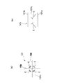
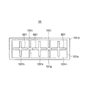
〔第1の実施形態〕
図20は、本発明の第1の実施形態に係る液晶表示装置1における層構造を示す模式図であり、このうち(a)は正面断面図、(b)は分解斜視図である。
[First Embodiment]
FIG. 20 is a schematic diagram showing a layer structure in the liquid
図20に示すように、液晶表示装置1は、垂直配向液晶セル(液晶セル)101と、この垂直配向液晶セル101の表裏両側に配置された第1及び第2の偏光板(第1及び第2の偏光層)102、103と、垂直配向液晶セル101と第1の偏光板102との間に配置された第1のλ/4板(第1の位相差板)122と、垂直配向液晶セル101と第2の偏光板103との間に配置された第2のλ/4板(第2の位相差板)123と、垂直配向液晶セル101と第1のλ/4板122との間に配置された第1の負の1軸の光学補償層(負の1軸の位相差を有する光学層)112と、垂直配向液晶セル101と第2のλ/4板123との間に配置された第2の負の1軸の光学補償層(負の1軸の位相差を有する光学層)113と、第1の偏光板102と第1のλ/4板122との間に配置された第1の偏光板支持体(負の1軸の位相差を有する光学層;支持体)132と、第2の偏光板103と第2のλ/4板123との間に配置された第2の偏光板支持体(負の1軸の位相差を有する光学層;支持体)133と、を備えている。
As shown in FIG. 20, the liquid
先ず、このうち、垂直配向液晶セル101について説明する。
First, the vertical alignment
図21乃至図23は垂直配向液晶セル101の模式図であり、このうち図21は正面切断端面図、図22は平面図、図23は斜視図である(ただし、TFT、配線電極などは図示していない)。
21 to 23 are schematic views of the vertically aligned
図21乃至図23に示すように、垂直配向液晶セル101は、相互に対向する一対の基板101a、101bと、これら一対の基板101a、101bに挟持された液晶層101cと、からなる。また、基板(以下、第1の基板)101aの液晶層101c側の面には、画素電極(電極)101eが形成されている。他方、基板(以下、第2の基板)101bの液晶層101c側の面には、共通電極(電極)101dが形成されている。つまり、一対の基板101a、101bは、各々電極を有している。これら画素電極101e及び共通電極101dは、本実施形態の場合、例えば、それぞれ透明電極からなる。つまり、垂直配向液晶セル101は、例えば、透過型である。
As shown in FIGS. 21 to 23, the vertical alignment
なお、第1の基板101aには、必要に応じてTFTなどのスイッチング素子(図示せず)、配線電極(図示せず)を設けてもよい。また、第2の基板101bには、必要に応じてカラーフィルター層(図示せず)、オーバーコート層(図示せず)を設けてもよい。
Note that a switching element (not shown) such as a TFT and a wiring electrode (not shown) may be provided on the
また、画素電極101eには、スリット101gが形成され、これにより電極不在部が構成されている。スリット101gが形成された結果、単位素子の画素電極101eは、図22及び図23に示すように、例えば、複数(例えば3つ)連なる矩形状部101hと、これら矩形状部101hを相互に連結するくびれ部101iと、からなる形状とされている。
Further, the
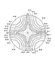
他方、共通電極101dには、スリット101fが形成され、これにより電極不在部が構成されている。スリット101fは、例えば、図22及び図23に示すように十字形状(+型)をなしている。このスリット101fは、基板101aの法線方向において、画素電極101eの各矩形状部101hと重なる位置に配置されている。つまり、例えば3つのスリット101fが、各矩形状部101hと対応する位置に配置されている。
On the other hand, a
なお、図24にスリット101f、101gの具体的な寸法の一例を示す。
FIG. 24 shows an example of specific dimensions of the
図24に示す例の場合、単位素子の寸法が110μm×330μmであり、矩形状部101hの寸法が90μ×100μmとなっている。そして、画素電極101eに形成されたスリット101g(電極不在部)の幅は、矩形状部101hの間隔部分で10μmとなっている。また、共通電極101dに形成された“+”型のスリット101f(電極不在部)は、84μm×75μmで、幅が10μmとなっている。
In the example shown in FIG. 24, the size of the unit element is 110 μm × 330 μm, and the size of the
また、以上のような構成の画素電極101e及び共通電極101dの上(液晶層101c側の面)には、それぞれ垂直配向膜(図示せず)が形成され、これら一対の垂直配向膜の間隔に、上記液晶層101cが配置されている。
Further, a vertical alignment film (not shown) is formed on the
液晶層101cには、負の誘電率異方性を持つ液晶(液晶分子)が充填されている。
The
なお、本実施形態の場合、例えば、液晶層101c内の液晶材のΔn=0.0741、セルギャップ(液晶層101cの厚み)dを4.5μmとした。従って、この場合の液晶層101cの厚み方向のリタデーションは、Δn・d=333nmとなる。なお、液晶層101cの厚み方向のリタデーションは、例えば、333nm±20nmであることが好ましく、333nm±15nmであることがより好ましい。
In the case of the present embodiment, for example, Δn = 0.0741 of the liquid crystal material in the
また、垂直配向液晶セル101の液晶は、電圧無印加時において、基板101a(及び基板101b)に対しほぼ垂直に配向している。対して、電圧を印加すると、画素電極101eの端部、あるいは電極不在部に斜め電界が発生し、液晶分子は基板101a(及び基板101b)に対して斜めに傾いて配向する。
Further, the liquid crystal of the vertically aligned
具体的には、電圧印加時、斜め電界の効果および液晶配向の連続性により、液晶層101cのセル厚方向中央付近の液晶(液晶分子E)は、図25に示すように、主に方位角方向45度、135度、225度、315度方向に傾いて4分割配向する。つまり、方位角45度方向に位置する液晶は方位角225度方向に倒れ、方位角135度方向に位置する液晶は方位角315度方向に倒れ、方位角225度方向に位置する液晶は方位角45度方向に倒れ、方位角315度方向に位置する液晶は方位角135度方向に倒れる。
Specifically, when a voltage is applied, the liquid crystal (liquid crystal molecule E) near the center in the cell thickness direction of the
このように、液晶層101cは、負の誘電率異方性を持つ液晶が充填されているとともに、電圧無印加時には垂直配向する一方で、電圧印加時には概ね4分割されるように4分割配向されている。
As described above, the
ここで、図25の示すように、共通電極101dに形成された“+”型のスリット101f(電極不在部)が、分割配向の境界となっている。従って、画素電極101eの各矩形状部101hと共通電極101dとの間の部分に、4つずつの領域(ドメイン)が形成されている。すなわち、スリット101fにより、液晶層101cにおける配向分割の境界(配向分割の対称軸)が形成されている。
Here, as shown in FIG. 25, the “+”-
垂直配向液晶セル101は、以上のように構成されている。
The vertical alignment
次に、その他の構成要素について説明する。 Next, other components will be described.
第1及び第2のλ/4板122、123は、それぞれ位相差がほぼλ/4に設定された位相差板である。
The first and second λ / 4
図20に示すように、第1のλ/4板122は、その遅相軸122aが、基板101a(或いは基板101b)の板面(単に、基板面)と平行となるように配置され、同様に、第2のλ/4板123も、その遅相軸123aが、基板面と平行となるように配置されている。
As shown in FIG. 20, the first λ / 4
更に、第1及び第2のλ/4板122、123は、第1のλ/4板122の遅相軸122aと、第2のλ/4板123の遅相軸123aと、が相互にほぼ直交状態となるように配置されている。
Further, the first and second λ / 4
すなわち、第1及び第2の位相差板は、基板面と平行な面内にそれぞれ遅相軸を有しているとともに、それぞれ位相差がほぼλ/4に設定され、且つ、相互の遅相軸がほぼ直交状態となるように配置されている。 That is, the first and second retardation plates each have a slow axis in a plane parallel to the substrate surface, the phase difference is set to approximately λ / 4, and the mutual retardation phase is set. It arrange | positions so that an axis | shaft may become a substantially orthogonal state.
また、第1の偏光板102は、その吸収軸102aが第1のλ/4板122の遅相軸122aに対して45度の角度となるように配置されている一方で、第2の偏光板103は、その吸収軸103aが第1のλ/4板123の遅相軸123aに対して45度の角度となるように配置されている。しかも、第1の偏光板102の吸収軸102aと、第2の偏光板103の吸収軸103aと、は相互に直交状態とされ、これら第1及び第2の偏光板102a、103aにより直交偏光板が構成されている。
The first
また、第1の偏光板支持体132は、第1の偏光板102の偏光層(図示略)を支持するものであり、同様に、第2の偏光板支持体133は、第2の偏光板103の偏光層(図示略)を支持するものである。
The first
これら偏光板支持体132、133は、例えば、TAC(トリアセチルセルロース)からなる。 These polarizing plate supports 132 and 133 are made of, for example, TAC (triacetyl cellulose).
第1の実施形態に係る液晶表示装置1は、以上のように構成されている。
The liquid
次に、このような液晶表示装置1において、偏光板支持体132、133として、その厚み方向のリタデーションが、例えばそれぞれ25nmのものを用いた場合で、第1及び第2の光学補償層112、113の厚み方向のリタデーションが25nm、50nm、75nm、100nm、125nm及び150nmの6種類の場合(つまり、第1及び第2の光学補償層112,113のリタデーションの和が50nm、100nm、150nm、200nm、250nm及び300nmの場合)に、それぞれどのような視角特性となるかを調べた結果について説明する。
Next, in such a liquid
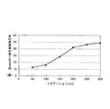
図26は、液晶表示装置1において、第1及び第2の偏光板102、103と、第1及び第2のλ/4板122、123と、第1及び第2の光学補償層112、113とを従来の配置角度(図13(c))で配置した場合に、一対の負の1軸の光学補償層112、113のリタデーションの和を横軸にとり、黒の透過率が最も高くなる方向を縦軸にとったグラフである。
FIG. 26 shows the first and second
図26の場合も、図14の場合と同様に、黒の透過率が高くなる方向が方位角45度の方向からずれ、しかも、そのずれ角度が、光学補償層112、113のリタデーションに応じて変化していることがわかる。
In the case of FIG. 26 as well, as in the case of FIG. 14, the direction in which the black transmittance increases is deviated from the direction of the azimuth angle of 45 degrees, and the deviation angle depends on the retardation of the
ただし、図26の場合には、図14と比べ、偏光板支持体132、133のTACのリタデーションの影響で、ずれ角度が若干異なる。 However, in the case of FIG. 26, the shift angle is slightly different due to the influence of the TAC retardation of the polarizing plate supports 132 and 133 as compared to FIG.
本発明者は、この“ずれ角度”をあらかじめ考慮し、該ずれ角度を相殺するように、第1及び第2の偏光板102、103、第1及び第2のλ/4板122、123、第1及び第2の光学補償層112、113の配置角度(単位:度)、及び、第1及び第2の光学補償層112、113の厚み方向のリタデーションを図27のように設定し、これら各構成要素を垂直配向液晶セル101に貼り付けた場合の視角特性を調べた。
The inventor considers this “deviation angle” in advance, and cancels the deviation angle, so that the first and second
つまり、液晶表示装置1の視角特性が対称となるように、第1及び第2の偏光板102、103の吸収軸102a、103aを液晶層101cにおける配向分割の対称軸に対してずらし、それに伴い第1及び第2のλ/4板122、123、第1及び第2の光学補償層112、113の配置角度もずらした場合の視覚特性を調べた。
That is, the
なお、図27の見方は、図15と同様である。 27 is the same as FIG.
図27に示す設定とした場合には、以下に説明するように、高コントラストの領域が狭いのは方位角45度、135度、225度、315度方向となり、かつx軸、y軸に関して対称な視角特性が得られた。 In the case of the setting shown in FIG. 27, as will be described below, the high-contrast region is narrow with azimuth angles of 45 degrees, 135 degrees, 225 degrees, and 315 degrees, and symmetric with respect to the x axis and the y axis. A good viewing angle characteristic was obtained.
図28には、第1及び第2の負の1軸の光学補償層112,113のそれぞれの厚み方向のリタデーションが75nm(和は150nm)の場合の結果(等コントラスト曲線)を示す。なお、図28の場合、各構成要素の配置角度は、図27に示すように、第1の偏光板102が20度、第1のλ/4板122が155度、第1の光学補償層112が110度、第2の光学補償層113が20度、第2のλ/4板123が65度、第2の偏光板103が110度である。つまり、偏光板支持体132、133の厚み方向のリタデーションがそれぞれ25nmであり、第1及び第2の光学補償層112、113の厚み方向のリタデーションがそれぞれ75nmであり、第1の偏光板102の吸収軸102aをx軸(配向分割の対称軸)に対しずらす角度が20度、第2の偏光板103の吸収軸103aをy軸(配向分割の対称軸)に対しずらす角度がやはり20度に設定されている。
FIG. 28 shows a result (isocontrast curve) when the retardation in the thickness direction of each of the first and second negative uniaxial
また、図28並びに以下に説明する図29乃至図31において、符号R11〜R18は、図6におけるのと同様であり、領域R16と領域R17との境界線がコントラスト=10の等コントラスト曲線である。 In FIG. 28 and FIGS. 29 to 31 described below, reference numerals R11 to R18 are the same as those in FIG. 6, and the boundary line between the region R16 and the region R17 is an isocontrast curve with contrast = 10. .
図28に示すように、第1及び第2の負の1軸の光学補償層112、113の厚み方向のリタデーションが75nm(和は150nm)の場合に図27に示す設定とすることにより、対称な視角特性が得られた。また、45度、135度、225度及び315度の方向でコントラスト>10となる極角方向の範囲が55度となった。
As shown in FIG. 28, when the retardation in the thickness direction of the first and second negative uniaxial
他方、図29には、図28の場合の比較例として、負の1軸の光学補償層112、113の厚み方向のリタデーションは図28の場合と同じであるが、第1及び第2の偏光板102、103と、第1及び第2のλ/4板122、123と、第1及び第2の光学補償板112、113とを従来の配置角度(図13(c))で配置した場合の視角特性を示す。この場合、図29に示すように、0度−180度方向、90度−270度方向に関して非対称な視角特性になっている。
On the other hand, in FIG. 29, as a comparative example in the case of FIG. 28, the retardation in the thickness direction of the negative uniaxial
また、図30には、第1及び第2の負の1軸の光学補償層112、113の厚み方向のリタデーションが100nm(和は200nm)の場合の結果を示す。なお、各構成要素の配置角度は、図27に示すように、第1の偏光板102が5度、第1のλ/4板122が140度、第1の光学補償層112が95度、第2の光学補償層113が5度、第2のλ/4板123が50度、第2の偏光板103が95度である。つまり、偏光板支持体132、133の厚み方向のリタデーションがそれぞれ25nmであり、第1及び第2の光学補償層112、113の厚み方向のリタデーションがそれぞれ100nmであり、第1の偏光板102の吸収軸102aをx軸(配向分割の対称軸)に対しずらす角度が5度、第2の偏光板103の吸収軸103aをy軸(配向分割の対称軸)に対しずらす角度がやはり5度に設定されている。
FIG. 30 shows the results when the retardation in the thickness direction of the first and second negative uniaxial
図30に示すように、第1及び第2の負の1軸の光学補償層112、113の厚み方向のリタデーションが100nm(和は200nm)の場合に図27に示す設定とすることにより、対称な視角特性が得られた。また、45度、135度、225度及び315度の方向でコントラスト>10となる極角方向の範囲が54度となった。
As shown in FIG. 30, when the retardation in the thickness direction of the first and second negative uniaxial
他方、図31には、図30の場合の比較例として、負の1軸の光学補償層112、113の厚み方向のリタデーションは図30の場合と同じであるが、第1及び第2の偏光板102、103と、第1及び第2のλ/4板122、123と、第1及び第2の光学補償板112、113とを従来の配置角度(図13(c))で配置した場合の視角特性を示す。この場合、図31に示すように、0度−180度方向、90度−270度方向に関して非対称な視角特性になっている。
On the other hand, in FIG. 31, as a comparative example in the case of FIG. 30, the retardation in the thickness direction of the negative uniaxial
なお、等コントラスト曲線の図示は省略するが、図27に示すその他の設定(第1及び第2の負の1軸の光学補償層112、113の厚み方向のリタデーションが25nm(和は50nm)、50nm(和は100nm)、125nm(和は250nm)、150nm(和は300nm))とした場合にも、図28及び図30と同様の結果が得られた。
Although illustration of the isocontrast curve is omitted, other settings shown in FIG. 27 (the retardation in the thickness direction of the first and second negative uniaxial
次に、図32及び図33に、第1及び第2の負の1軸の光学補償層112、113の厚み方向のリタデーションが75nm(和は150nm)で図27に示す設定とした場合の極角−透過率特性の電圧依存性を示す。このうち図32は、方位角0度―180度方向の極角−透過率特性の電圧依存性を示し、図33は、方位角45度―135度方向の極角−透過率特性の電圧依存性を示す。
Next, FIG. 32 and FIG. 33 show the poles when the retardation in the thickness direction of the first and second negative uniaxial
これら図32及び図33に示すように、(方位角45度―135度方向(図33)では高電圧印加時の階調反転が見られたものの)、何れの場合にも黒の透過率(電圧無印加時)の上昇を抑制することができている。 As shown in FIGS. 32 and 33 (in the azimuth angle direction of 45 degrees to 135 degrees (FIG. 33), gradation inversion was observed when a high voltage was applied), in either case, the black transmittance ( An increase in voltage (when no voltage is applied) can be suppressed.
次に、第1及び第2の偏光板支持体132,133の厚み方向のリタデーションをそれぞれ25nmから50nmに変更した場合について説明する。 Next, a case where the retardation in the thickness direction of the first and second polarizing plate supports 132 and 133 is changed from 25 nm to 50 nm will be described.
図34は、第1及び第2の偏光板支持体132,133の厚み方向のリタデーションがそれぞれ50nmの場合に、第1及び第2の偏光板102、103と、第1及び第2のλ/4板122、123と、第1及び第2の光学補償板112、113とを従来の配置角度(図13(c))で配置した場合に、一対の負の1軸の光学補償層112、113のリタデーションの和を横軸にとり、黒の透過率が最も高くなる方向を縦軸にとったグラフである。
FIG. 34 shows the first and second
図34の場合も、図26の場合と同様に、黒の透過率が高くなる方向が方位角45度の方向からずれ、しかも、そのずれ角度が、光学補償層112、113のリタデーションに応じて変化していることがわかる。
In the case of FIG. 34 as well, as in FIG. 26, the direction in which the black transmittance increases is deviated from the direction of the azimuth angle of 45 degrees, and the deviation angle depends on the retardation of the
ただし、図34の場合には、図26と比べ、各偏光板支持体132、133のTACのリタデーションが25nmから50nmへと大きくなっている影響で、ずれ角度が若干異なる。
However, in the case of FIG. 34, as compared with FIG. 26, the shift angle is slightly different due to the influence that the retardation of TAC of each
この“ずれ角度”をあらかじめ考慮し、該ずれ角度を相殺するように、第1及び第2の偏光板102、103、第1及び第2のλ/4板122、123、第1及び第2の光学補償層112、113の配置角度(単位:度)、及び、第1及び第2の光学補償層112、113の厚み方向のリタデーションを図35のように設定し、これら各構成要素を垂直配向液晶セル101に貼り付けた場合の視角特性を調べた。なお、この図35の見方は、図15及び図27と同様である。
Considering this “deviation angle” in advance, the first and second
図35に示す設定とした場合、以下に説明するように、図27に示す設定とした場合と同様に、高コントラストの領域が狭いのは方位角45度、135度、225度、315度方向となり、かつx軸、y軸に関して対称な視角特性が得られた。 When the setting shown in FIG. 35 is used, as described below, as in the setting shown in FIG. 27, the high-contrast area is narrow in the directions of 45 degrees, 135 degrees, 225 degrees, and 315 degrees. In addition, a viewing angle characteristic symmetric with respect to the x-axis and the y-axis was obtained.
図36には、第1及び第2の負の1軸の光学補償層112,113のそれぞれの厚み方向のリタデーションが50nm(和は100nm)の場合の結果(等コントラスト曲線)を示す。なお、図36の場合、各構成要素の配置角度は、図35に示すように、第1の偏光板102が28度、第1のλ/4板122が163度、第1の光学補償層112が118度、第2の光学補償層113が28度、第2のλ/4板123が73度、第2の偏光板103が118度である。
FIG. 36 shows a result (isocontrast curve) when the retardation in the thickness direction of each of the first and second negative uniaxial
また、図36並びに以下に説明する図37乃至図39において、符号R11〜R18は、図6におけるのと同様であり、領域R16と領域R17との境界線がコントラスト=10の等コントラスト曲線である。 In FIG. 36 and FIGS. 37 to 39 described below, reference numerals R11 to R18 are the same as those in FIG. 6, and the boundary line between the region R16 and the region R17 is an isocontrast curve with contrast = 10. .
図36に示すように、第1及び第2の負の1軸の光学補償層112、113の厚み方向のリタデーションが50nm(和は100nm)の場合に図35に示す設定とすることにより、対称な視角特性が得られた。また、45度、135度、225度及び315度の方向でコントラスト>10となる極角方向の範囲が50度となった。
As shown in FIG. 36, when the retardation in the thickness direction of the first and second negative uniaxial
他方、図37には、図36の場合の比較例として、負の1軸の光学補償層112、113の厚み方向のリタデーションは図36の場合と同じであるが、第1及び第2の偏光板102、103と、第1及び第2のλ/4板122、123と、第1及び第2の光学補償板112、113とを従来の配置角度(図13(c))で配置した場合の視角特性を示す。この場合、図37に示すように、0度−180度方向、90度−270度方向に関して非対称な視角特性になっている。
On the other hand, in FIG. 37, as a comparative example in the case of FIG. 36, the retardation in the thickness direction of the negative uniaxial
また、図38には、第1及び第2の負の1軸の光学補償層112、113の厚み方向のリタデーションが75nm(和は150nm)の場合の結果を示す。なお、各構成要素の配置角度は、図35に示すように、第1の偏光板102が16度、第1のλ/4板122が151度、第1の光学補償層112が106度、第2の光学補償層113が16度、第2のλ/4板123が61度、第2の偏光板103が106度である。
FIG. 38 shows the results when the retardation in the thickness direction of the first and second negative uniaxial
図38に示すように、第1及び第2の負の1軸の光学補償層112、113の厚み方向のリタデーションが75nm(和は150nm)の場合に図35に示す設定とすることにより、対称な視角特性が得られた。また、45度、135度、225度及び315度の方向でコントラスト>10となる極角方向の範囲が53度となった。
As shown in FIG. 38, when the retardation in the thickness direction of the first and second negative uniaxial
他方、図39には、図38の場合の比較例として、負の1軸の光学補償層112、113の厚み方向のリタデーションは図38の場合と同じであるが、第1及び第2の偏光板102、103と、第1及び第2のλ/4板122、123と、第1及び第2の光学補償板112、113とを従来の配置角度(図13(c))で配置した場合の視角特性を示す。この場合、図39に示すように、0度−180度方向、90度−270度方向に関して非対称な視角特性になっている。
On the other hand, in FIG. 39, as a comparative example in the case of FIG. 38, the retardation in the thickness direction of the negative uniaxial
なお、等コントラスト曲線の図示は省略するが、図35に示すその他の設定(第1及び第2の負の1軸の光学補償層112、113の厚み方向のリタデーションが25nm(和は50nm)、50nm(和は100nm)、125nm(和は250nm)、150nm(和は300nm))とした場合にも、図36及び図38と同様の結果が得られた。
Although illustration of the isocontrast curve is omitted, other settings shown in FIG. 35 (the retardation in the thickness direction of the first and second negative uniaxial
以上のように、第1の実施形態に係る液晶表示装置1によれば、該液晶表示装置1の視角特性が対称となるように、第1及び第2の偏光板102、103の吸収軸102a、103aを液晶層101cにおける配向分割の対称軸に対してずらし、それに伴い第1及び第2のλ/4板122、123、第1及び第2の光学補償層112、113の配置角度もずらしているので、x軸並びにy軸に対して対称な視角特性が得られる。更に、第1及び第2の偏光板102、103の吸収軸102a、103aに対し斜め方向45度の方向(45度、135度、225度、315度方向)における黒の白浮き(黒表示時の光漏れ)を抑制できる。
As described above, according to the liquid
<液晶セルのスリット形状の変形例>
図47及び図48に垂直配向液晶セルの変形例を示す。
<Modified example of slit shape of liquid crystal cell>
47 and 48 show modifications of the vertical alignment liquid crystal cell.
ここで、垂直配向液晶セルにおけるスリットの面積及び幅の設定をどのような観点で行うべきかについて説明する。 Here, the viewpoint of setting the area and width of the slit in the vertically aligned liquid crystal cell will be described.
スリットに近接している液晶は、画素電極と共通電極の両方にはさまれた液晶に比べ電圧がかかりにくくなっている。そのためスリット部の光利用効率は低くなっている。 The liquid crystal close to the slit is less likely to be applied with voltage than the liquid crystal sandwiched between both the pixel electrode and the common electrode. Therefore, the light use efficiency of the slit portion is low.
よって、透過率を稼ぎたい場合はできるだけスリットの領域を減らす必要がある。そのような観点から、図47に示す垂直配向セル47は、図22の場合と比べて、単位面積当たりの矩形状部101hの数を減らすことにより、スリットの領域(面積)を減らし、透過率を優先した形状となっている。
Therefore, in order to increase the transmittance, it is necessary to reduce the slit area as much as possible. From such a viewpoint, the
他方、応答時間を良くするためには斜め電界にさらされる液晶を増やす必要がある。そのような観点から、図48に示す垂直配向セル48は、図22の場合と比べて、単位面積当たりの矩形状部101hの数を増やすことにより、スリット101g及び101fの領域(面積)を増やした形状となっている。ただし、垂直配向セル48の場合、スリット101g及び101fの面積が増えた分、光利用効率は下がる。
On the other hand, in order to improve the response time, it is necessary to increase the number of liquid crystals exposed to an oblique electric field. From such a viewpoint, the
また、指押しなどの外部からの圧力に対する配向の安定性の面から考えるとスリット101g及び101fの幅は広いほうが良い。その理由について図49及び図50を参照して説明する。スリット101g及び101fは、分割配向の境界としての役割を果たし、スリット101g及び101fを境界とした両側部分では、液晶の倒れる方向が相互に異なる。このため、スリット101g及び101fに対応する位置の液晶は、電圧印加時にも中立状態(つまり垂直配向状態のまま)となる。よって、スリット101g及び101fの幅が広い場合(図49)の方が、狭い場合(図50)の場合よりも、中立状態のままの液晶の量が増え、スリット101g及び101fに対応する部分は外圧に対する抗力が強まる。しかしながらスリット101g及び101fの幅が広すぎると透過率が下がる。透過率を稼ぐには幅を狭くしてスリット101g及び101fの面積をできるだけ小さくすればよいが、幅が狭すぎると分割配向が維持できなくなる。
In view of stability of orientation with respect to external pressure such as finger pressing, the
本発明者は、これらのことがらを勘案し、スリットの幅は6μmから12μmの範囲が好ましい、と結論を得た。 The present inventor has taken these points into consideration and concluded that the slit width is preferably in the range of 6 μm to 12 μm.
なお、図51には、図47に示す垂直配向液晶セル47の場合における好適な寸法の一例を示し、図52には、図48に示す垂直配向液晶セル48の場合における好適な寸法の一例を示す。
FIG. 51 shows an example of suitable dimensions in the case of the vertical alignment
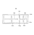
〔第2の実施形態〕
図40は本発明の第2の実施形態に係る液晶表示装置10を示す模式図であり、このうち(a)は正面断面図、(b)は分解斜視図である。
[Second Embodiment]
FIG. 40 is a schematic view showing a liquid
図40に示すように、第2の実施形態に係る液晶表示装置10は、図20の液晶表示装置1と比べて、第2の負の1軸の光学補償層113を備えていない点でのみ異なり、その他の点では同様に構成されている。
As shown in FIG. 40, the liquid
なお、第1及び第2の偏光板支持体132、133の厚み方向のリタデーションは、例えば、それぞれ25nmとした。 The retardation in the thickness direction of the first and second polarizing plate supports 132 and 133 is, for example, 25 nm, respectively.
以下、第2の実施形態において、第1の光学補償層112の厚み方向のリタデーションが25nm、50nm、75nm、100nm、125nm及び150nmの6種類の場合にそれぞれどのような視角特性となるかを調べた結果について説明する。
Hereinafter, in the second embodiment, the viewing angle characteristics are examined when the thickness direction retardation of the first
図41は、第2の実施形態において、第1及び第2の偏光板102、103と、第1及び第2のλ/4板122、123と、第1の光学補償板112とを従来の配置角度(図13(c))で配置した場合に、負の1軸の光学補償層112のリタデーションを横軸にとり、黒の透過率が最も高くなる方向を縦軸にとったグラフである。
In FIG. 41, in the second embodiment, the first and second
図41の場合も、図34の場合と同様に、黒の透過率が高くなる方向が方位角45度の方向からずれ、しかも、そのずれ角度が、光学補償層112、113のリタデーションに応じて変化していることがわかる。
In the case of FIG. 41 as well, as in FIG. 34, the direction in which the black transmittance increases is deviated from the direction of the azimuth angle of 45 degrees, and the deviation angle depends on the retardation of the
なお、図41の場合には、図34と比べ、第2の負の1軸の光学補償層113を備えていない影響で、ずれ角度が異なる。
In the case of FIG. 41, the shift angle is different from that of FIG. 34 due to the fact that the second negative uniaxial
この“ずれ角度”をあらかじめ考慮し、該ずれ角度を相殺するように、第1及び第2の偏光板102、103、第1及び第2のλ/4板122、123、第1光学補償層112の配置角度(単位:度)、及び、第1の光学補償層112の厚み方向のリタデーションを図42のように設定し、これら各構成要素を垂直配向液晶セル101に貼り付けた場合の視角特性を調べた。なお、この図42の見方は、図15、図27及び図35と同様である。
Considering this “shift angle” in advance, the first and second
図43には、第1の負の1軸の光学補償層112の厚み方向のリタデーションが50nmの場合の結果(等コントラスト曲線)を示す。なお、図43の場合、各構成要素の配置角度は、図42に示すように、第1の偏光板102が28度、第1のλ/4板122が163度、第1の光学補償層112が118度、第2のλ/4板123が73度、第2の偏光板103が118度である。
FIG. 43 shows a result (isocontrast curve) when the thickness direction retardation of the first negative uniaxial
また、図43及び以下に説明する図44において、符号R11〜R18は、図6におけるのと同様であり、領域R16と領域R17との境界線がコントラスト=10の等コントラスト曲線である。 In FIG. 43 and FIG. 44 described below, reference numerals R11 to R18 are the same as those in FIG. 6, and the boundary line between the region R16 and the region R17 is an isocontrast curve with contrast = 10.
図43に示すように、第1の負の1軸の光学補償層112の厚み方向のリタデーションが50nmの場合に図42に示す設定とすることにより、対称な視角特性が得られた。また、45度、135度、225度及び315度の方向でコントラスト>10となる極角方向の範囲が44度となった。
As shown in FIG. 43, when the retardation in the thickness direction of the first negative uniaxial
また、図44には、第1の負の1軸の光学補償層112の厚み方向のリタデーションが75nmの場合の結果(等コントラスト曲線)を示す。なお、図44の場合、各構成要素の配置角度は、図42に示すように、第1の偏光板102が28度、第1のλ/4板122が163度、第1の光学補償層112が118度、第2のλ/4板123が73度、第2の偏光板103が118度である。
FIG. 44 shows a result (isocontrast curve) when the retardation in the thickness direction of the first negative uniaxial
図44に示すように、第1の負の1軸の光学補償層112の厚み方向のリタデーションが75nmの場合に図42に示す設定とすることにより、ほぼ対称な視角特性が得られた。なお、45度、135度、225度及び315度の方向でコントラスト>10となる極角方向の範囲は46度となり、図43の場合よりも若干広がったが、対称性は図43の場合よりも若干悪くなった。
As shown in FIG. 44, when the retardation in the thickness direction of the first negative uniaxial
次に、図45及び図46に、第1の負の1軸の光学補償層112の厚み方向のリタデーションが50nmで図42に示す設定とした場合の極角−透過率特性の電圧依存性を示す。このうち図45は、方位角0度―180度方向の極角−透過率特性の電圧依存性を示し、図46は、方位角45度―135度方向の極角−透過率特性の電圧依存性を示す。
Next, FIGS. 45 and 46 show the voltage dependence of polar angle-transmittance characteristics when the retardation in the thickness direction of the first negative uniaxial
これら図45及び図46に示す何れの場合にも、図32及び図33の場合と比べて、極角変化に伴う黒の透過率(電圧無印加時)の若干の上昇が見られるものの、何れの場合にも黒の透過率の上昇を抑制できている。 In any of the cases shown in FIGS. 45 and 46, although a slight increase in the black transmittance (when no voltage is applied) due to the change in polar angle is seen compared to the cases of FIGS. In this case, an increase in black transmittance can be suppressed.
また、図46に示すように、方位角45度―135度方向における高電圧印加時の階調反転は、図33の場合と比べて抑制できている。 Further, as shown in FIG. 46, the gradation inversion at the time of applying a high voltage in the direction of the azimuth angle of 45 degrees to 135 degrees can be suppressed compared to the case of FIG.
以上のように、第2の実施形態によれば、上記の第1の実施形態と同様の効果が得られる他、第1の実施形態の場合と比べ、第2の負の1軸の光学補償層113を省いた構成になっているので、その分だけコストを低減できる。また、第1の実施形態の場合と比べ、方位角45度―135度方向における高電圧印加時の階調反転を抑制できる。
As described above, according to the second embodiment, the same effects as those of the first embodiment can be obtained, and the second negative uniaxial optical compensation can be obtained as compared with the case of the first embodiment. Since the
〔第3の実施形態〕
上記の各実施形態では、液晶セルが透過型である例を説明したが、第4の実施形態では、半透過型である例について説明する。
[Third Embodiment]
In each of the above embodiments, an example in which the liquid crystal cell is a transmissive type has been described. In the fourth embodiment, an example in which a liquid crystal cell is a transflective type will be described.
図53及び図54は、第3の実施形態に係る液晶表示装置の垂直配向液晶セル53を示す模式図であり、このうち図53は平面図、図54は斜視図を示す(ただし、TFT、配線電極などは図示していない)。
53 and 54 are schematic views showing a vertical alignment
図53及び図54に示すように、垂直配向液晶セル53においては、各単位素子内の画素電極101eが反射電極部(反射部)531と透明電極部(透過部)532とからなり、垂直配向液晶セル53は、半透過型となっている。
As shown in FIGS. 53 and 54, in the vertical alignment
なお、図54では、反射電極部531を、その表面形状を平面として図示しているが、例えば、本実施形態の場合、反射特性を改善するために、反射電極部531の表面は凹凸形状にしているものとする。
In FIG. 54, the
また、図53及び図54に示すように、共通電極101dにおいて、反射電極部531及び透明電極部531とそれぞれ対向する部分には、スリット101fが形成され、これにより、反射電極部531及び透明電極部531がそれぞれ4分割配向している。
As shown in FIGS. 53 and 54, in the
また、垂直配向液晶セル53においては、反射電極部531の厚み方向のリタデーションは、透明電極部532の厚み方向のリタデーションよりも小さい値に設定されている。例えば、液晶材のΔn=0.0741とした場合、透明電極部532のセルギャップを4.5μmとした。この場合、反射電極部531のリタデーションは、該反射電極部531の凹凸形状の出来上り具合にもよるが、例えば、透明電極部532の44%程度であることが好ましい。このため、液晶層のリタデーションは、例えば、透明電極部532においては333nm±20nm(より好ましくは±15nm)とし、反射電極部531においては150nm±20nm(より好ましくは±15nm)とする。
In the vertical alignment
このように反射電極部531の厚み方向のリタデーションを透明電極部532の厚み方向のリタデーションよりも小さい値に設定することにより、反射と透過ともに良好な表示ができるという効果が得られる。
In this way, by setting the retardation in the thickness direction of the
なお、反射電極部531には、対応するスリット101fが無くても視角特性が悪くないが、反射電極部531の表面が凹凸形状になっているので、他に配向を規制するものがないと配向の再現性が弱く、ざらついて見えることがある。そこで共通電極101dにおいて反射電極部531と対向する部分にもスリット101fを形成し、配向の再現性を高めている。
The viewing angle characteristics of the
次に、第1の実施形態に係る液晶表示装置1における垂直配向液晶セル101に変えて第4の実施形態の垂直配向液晶セル53を用い、第1及び第2の偏光板支持体132、133の厚み方向のリタデーションがそれぞれ25nmである第1及び第2の偏光板102、103を用いた場合の視角特性について調べた結果を説明する。
Next, the vertical alignment
なお、第1、第2の負の1軸の光学補償層112、113のそれぞれの厚み方向のリタデーションは100nm(和は200nm)とした。
The retardation in the thickness direction of each of the first and second negative uniaxial
その結果、透過の特性に関しては、対称な視角特性が得られた。また45度、135度、225度及び315度の方向でコントラスト>10となる極角方向の範囲は54度となった。 As a result, a symmetrical viewing angle characteristic was obtained with respect to the transmission characteristic. Further, the polar angle range in which the contrast> 10 in the directions of 45 degrees, 135 degrees, 225 degrees, and 315 degrees was 54 degrees.
また、反射の特性に関しては、反射の黒の反射率が抑えられ、コントラストの良い特性が得られた。またざらついて見えることも無かった。 As for the reflection characteristics, the black reflectance of reflection was suppressed and a characteristic with good contrast was obtained. Also, it didn't look rough.
以上のように第3の実施形態によれば、上記の第1の実施形態と同様の結果が得られる他、反射の黒の反射率を抑制でき、コントラストの良い特性が得られ、しかも、ざらついて見えることも無い。 As described above, according to the third embodiment, the same result as in the first embodiment can be obtained, the reflectance of reflected black can be suppressed, and a characteristic with good contrast can be obtained. I don't see it.
〔第4の実施形態〕
上記の各実施形態では、電極に形成されたスリットにより配向分割の境界が形成された例を説明したが、第4の実施形態では、電極に設けられた絶縁性の構造物により配向分割の境界が形成されている例について説明する。
[Fourth Embodiment]
In each of the above embodiments, the example in which the alignment division boundary is formed by the slit formed in the electrode has been described. However, in the fourth embodiment, the alignment division boundary is formed by the insulating structure provided in the electrode. An example in which is formed will be described.
図55及び図56に示すように、本実施形態に係る液晶表示装置の垂直配向液晶セル55は、上記の第1の実施形態の垂直配向液晶セル101と比べて、その共通電極101dにスリット101fが形成されておらず、該スリット101fの代わりに絶縁性の構造物551が形成されている点でのみ異なり、その他の点では垂直配向液晶セル101と同様に構成されている。
As shown in FIGS. 55 and 56, the vertical alignment
すなわち、垂直配向液晶セル55の共通電極101dの液晶層101c側の面には、絶縁性の構造物551が形成されている。
That is, the insulating
なお、構造物551の平面形状及び形成位置は、垂直配向液晶セル101におけるスリット101fと同様である。つまり、構造物551は、その平面形状が“+型”であり、基板101aの法線方向において、画素電極101eの各矩形状部101hと重なる位置に配置されている。
Note that the planar shape and formation position of the
このような構造物551により、液晶層101cにおける配向分割の境界が形成されている。
Such a
また、構造物551により、垂直配向液晶セル55が補強されるので、指押しなどの外部からの圧力に対する配向の安定性を得ることもできる。
Further, since the vertically aligned
構造物551は、例えば、アクリル系感光性材料を用いて形成することができる。
The
なお、矩形状部101hの態様が図47の垂直配向セル47と同様である場合には、図57に示すように構造物551を形成すると良く、矩形状部101hの態様が図48の垂直配向セル48と同様である場合には、図58に示すように構造物551を形成すると良い。
When the aspect of the
以上のような第4の実施形態によれば、共通電極101dの液晶層101c側の面に絶縁性の構造物551が形成されているので、この構造物551により、液晶層101cにおける配向分割の境界を好適に形成でき、しかも、指押しなどの外部からの圧力に対する配向の安定性を得ることもできる。
According to the fourth embodiment as described above, since the insulating
なお、負の1軸の位相差を有する光学層の配置位置は、上記の例に限らず、第1のλ/4板122と垂直配向液晶セル101との間、第2のλ/4板123と垂直配向液晶セル101との間、第1のλ/4板122と第1の偏光板102との間、及び、第2のλ/4板123と第2の偏光板103との間、のうちの少なくとも何れか1箇所であれば、どのようであっても良い。
The arrangement position of the optical layer having a negative uniaxial retardation is not limited to the above example, and the second λ / 4 plate is disposed between the first λ / 4
また、負の1軸の位相差を有する各光学層のリタデーションの値は、上記の例に限らず任意であり、それに伴い各構成要素の配置角度も適宜に変更可能であるのは勿論である。 Further, the retardation value of each optical layer having a negative uniaxial phase difference is not limited to the above example, and it is a matter of course that the arrangement angle of each component can be changed as appropriate. .
また、配向分割の境界となる“+型”のスリット101fは、共通電極101dだけでなく画素電極101eにも形成することとしてもよいし、共通電極101dには形成せずに画素電極101eのみに形成することとしてもよい。
Further, the “+ -type”
また、絶縁性の構造物551についても同様に、共通電極101dだけでなく画素電極101eにも形成することとしてもよいし、共通電極101dには形成せずに画素電極101eのみに形成することとしてもよい。
Similarly, the insulating
また、絶縁性の構造物551は、電極(共通電極101d或いは画素電極101e)にスリット101fを形成した上で、該スリット101f内に配置するようにしてもよい。
Further, the insulating
1 液晶表示装置
101 垂直配向液晶セル(液晶セル)
101d 共通電極(電極)
101e 画素電極(電極)
101a 基板
101b 基板
101c 液晶層
102 第1の偏光板(第1の偏光層)
102a 吸収軸
103 第2の偏光板(第2の偏光層)
103a 吸収軸
122 第1のλ/4板(第1の位相差板)
122a 遅相軸
123 第2のλ/4板(第2の位相差板)
123a 遅相軸
112 負の1軸の光学補償層(負の1軸の位相差を有する光学層;特に、第1の位相差板と液晶セルとの間に配置された光学層)
113 負の1軸の光学補償層(負の1軸の位相差を有する光学層;特に、第2の位相差板と液晶セルとの間に配置された光学層)
132 偏光板支持体(負の1軸の位相差を有する光学層;特に、第1の位相差板と第1の偏光層との間に配置された光学層)
133 偏光板支持体(負の1軸の位相差を有する光学層;特に、第2の位相差板と第2の偏光層との間に配置された光学層)
10 液晶表示装置
47 垂直配向液晶セル(液晶セル)
48 垂直配向液晶セル(液晶セル)
53 垂直配向液晶セル(液晶セル)
531 反射電極部(反射部)
532 透明電極部(透過部)
101f スリット
101g スリット
55 垂直配向液晶セル(液晶セル)
551 構造物
DESCRIPTION OF
101d Common electrode (electrode)
101e Pixel electrode (electrode)
101a
122a
123a
113 Negative uniaxial optical compensation layer (optical layer having negative uniaxial retardation; in particular, an optical layer disposed between the second retardation plate and the liquid crystal cell)
132 Polarizing plate support (optical layer having negative uniaxial retardation; in particular, optical layer disposed between first retardation plate and first polarizing layer)
133 Polarizing plate support (optical layer having negative uniaxial retardation; in particular, an optical layer disposed between the second retardation plate and the second polarizing layer)
10 Liquid
48 Vertical alignment liquid crystal cell (liquid crystal cell)
53 Vertical alignment liquid crystal cell (liquid crystal cell)
531 Reflective electrode part (reflective part)
532 Transparent electrode part (transmission part)
101f slit 101g slit 55 vertical alignment liquid crystal cell (liquid crystal cell)
551 Structure
Claims (2)
前記液晶セルの両側に配置された第1及び第2の偏光層と、
前記第1の偏光層と前記液晶セルとの間に配置された第1の位相差板と、
前記第2の偏光層と前記液晶セルとの間に配置された第2の位相差板と、
前記第1の位相差板と前記液晶セルとの間、前記第2の位相差板と前記液晶セルとの間、前記第1の位相差板と前記第1の偏光層との間、及び、前記第2の位相差板と第2の偏光層との間、にそれぞれ配置された、負の1軸の位相差を有する第1ないし第4の光学層と、
を備える液晶表示装置であって、
前記第1及び第2の位相差板は、前記基板と平行な面内にそれぞれ遅相軸を有しているとともに、それぞれ位相差がほぼλ/4に設定され、且つ、相互の遅相軸がほぼ直交状態となるように配置され、
前記第1の偏光層の吸収軸は、前記第1の位相差板の遅相軸に対してほぼ45度の角度となり、且つ、前記第2の偏光層の吸収軸に対してほぼ90度の角度となるように配置され、
前記液晶層は、負の誘電率異方性を持つ液晶が充填されているとともに、電圧無印加時には垂直配向する一方で、電圧印加時には概ね4分割されるように4分割配向され、
前記液晶セルの前記基板の一方に、前記電極として反射電極部と透明電極部とが形成され、前記液晶層のリタデーションが、前記透明電極部においては333nm±20nmであり、前記反射電極部においては150nm±20nmであり、
前記第1および前記第2の光学層のそれぞれの厚み方向のリタデーションが75nmであり、前記第3および第4の光学層のそれぞれの厚み方向のリタデーションが25nmであり、前記第1の偏光層の前記吸収軸を前記液晶層における配向分割の対称軸の一つであるx軸に対してずらす角度が20度であり、前記第1の位相差板の前記遅相軸を前記x軸に対してずらす角度が155度であり、前記第1の光学層の遅相軸を前記x軸に対してずらす角度が110度であり、前記第2の光学層の遅相軸を前記x軸に対してずらす角度が20度であり、前記第2の位相差板の前記遅相軸を前記x軸に対してずらす角度が65度であり、前記第2の偏光層の前記吸収軸を前記x軸に対してずらす角度が110度である、ことを特徴とする液晶表示装置。 A liquid crystal cell comprising a pair of substrates each having an electrode and a liquid crystal layer sandwiched between the pair of substrates;
First and second polarizing layers disposed on both sides of the liquid crystal cell;
A first retardation plate disposed between the first polarizing layer and the liquid crystal cell;
A second retardation plate disposed between the second polarizing layer and the liquid crystal cell;
Between the first retardation plate and the liquid crystal cell, between the second retardation plate and the liquid crystal cell, between the first retardation plate and the first polarizing layer, and the second between the phase difference plate and the second polarizing layer, the disposed respectively, the first to fourth optical layer having a phase difference of negative uniaxial,
A liquid crystal display device comprising:
Each of the first and second retardation plates has a slow axis in a plane parallel to the substrate, each of which has a phase difference of approximately λ / 4, and a mutual slow axis. Are arranged so as to be almost orthogonal,
The absorption axis of the first polarizing layer is an angle of approximately 45 degrees with respect to the slow axis of the first retardation plate, and is approximately 90 degrees with respect to the absorption axis of the second polarizing layer. Placed at an angle,
The liquid crystal layer is filled with liquid crystal having a negative dielectric anisotropy, and is vertically aligned when no voltage is applied, while being divided into four so as to be approximately divided into four when a voltage is applied,
A reflective electrode part and a transparent electrode part are formed as the electrodes on one of the substrates of the liquid crystal cell, and the retardation of the liquid crystal layer is 333 nm ± 20 nm in the transparent electrode part, and in the reflective electrode part 150 nm ± 20 nm,
The retardation in the thickness direction of each of the first and second optical layers is 75 nm, the retardation in the thickness direction of each of the third and fourth optical layers is 25 nm, and the retardation of the first polarizing layer An angle for shifting the absorption axis with respect to the x axis, which is one of the symmetry axes of the alignment division in the liquid crystal layer, is 20 degrees, and the slow axis of the first retardation plate is set with respect to the x axis. The angle of shifting is 155 degrees, the angle of shifting the slow axis of the first optical layer with respect to the x axis is 110 degrees, and the slow axis of the second optical layer is set with respect to the x axis. The angle of shifting is 20 degrees, the angle of shifting the slow axis of the second retardation plate with respect to the x axis is 65 degrees, and the absorption axis of the second polarizing layer is set to the x axis. an angle of 110 degrees shifted against, a liquid crystal display instrumentation, characterized in that .
前記液晶セルの両側に配置された第1及び第2の偏光層と、
前記第1の偏光層と前記液晶セルとの間に配置された第1の位相差板と、
前記第2の偏光層と前記液晶セルとの間に配置された第2の位相差板と、
前記第1の位相差板と前記液晶セルとの間、前記第2の位相差板と前記液晶セルとの間、前記第1の位相差板と前記第1の偏光層との間、及び、前記第2の位相差板と第2の偏光層との間、にそれぞれ配置された、負の1軸の位相差を有する第1ないし第4の光学層と、
を備える液晶表示装置であって、
前記第1及び第2の位相差板は、前記基板と平行な面内にそれぞれ遅相軸を有しているとともに、それぞれ位相差がほぼλ/4に設定され、且つ、相互の遅相軸がほぼ直交状態となるように配置され、
前記第1の偏光層の吸収軸は、前記第1の位相差板の遅相軸に対してほぼ45度の角度となり、且つ、前記第2の偏光層の吸収軸に対してほぼ90度の角度となるように配置され、
前記液晶層は、負の誘電率異方性を持つ液晶が充填されているとともに、電圧無印加時には垂直配向する一方で、電圧印加時には概ね4分割されるように4分割配向され、
前記液晶セルの前記基板の一方に、前記電極として反射電極部と透明電極部とが形成され、前記液晶層のリタデーションが、前記透明電極部においては333nm±20nmであり、前記反射電極部においては150nm±20nmであり、
前記第1および前記第2の光学層のそれぞれの厚み方向のリタデーションが100nmであり、前記第3および第4の光学層のそれぞれの厚み方向のリタデーションが25nmであり、前記第1の偏光層の前記吸収軸を前記液晶層における配向分割の対称軸の一つであるx軸に対してずらす角度が5度であり、前記第1の位相差板の前記遅相軸を前記x軸に対してずらす角度が140度であり、前記第1の光学層の遅相軸を前記x軸に対してずらす角度が95度であり、前記第2の光学層の遅相軸を前記x軸に対してずらす角度が5度であり、前記第2の位相差板の前記遅相軸を前記x軸に対してずらす角度が50度であり、前記第2の偏光層の前記吸収軸を前記x軸に対してずらす角度が95度である、ことを特徴とする液晶表示装置。 A liquid crystal cell comprising a pair of substrates each having an electrode and a liquid crystal layer sandwiched between the pair of substrates;
First and second polarizing layers disposed on both sides of the liquid crystal cell;
A first retardation plate disposed between the first polarizing layer and the liquid crystal cell;
A second retardation plate disposed between the second polarizing layer and the liquid crystal cell;
Between the first retardation plate and the liquid crystal cell, between the second retardation plate and the liquid crystal cell, between the first retardation plate and the first polarizing layer, and the second between the phase difference plate and the second polarizing layer, the disposed respectively, the first to fourth optical layer having a phase difference of negative uniaxial,
A liquid crystal display device comprising:
Each of the first and second retardation plates has a slow axis in a plane parallel to the substrate, each of which has a phase difference of approximately λ / 4, and a mutual slow axis. Are arranged so as to be almost orthogonal,
The absorption axis of the first polarizing layer is an angle of approximately 45 degrees with respect to the slow axis of the first retardation plate, and is approximately 90 degrees with respect to the absorption axis of the second polarizing layer. Placed at an angle,
The liquid crystal layer is filled with liquid crystal having a negative dielectric anisotropy, and is vertically aligned when no voltage is applied, while being divided into four so as to be approximately divided into four when a voltage is applied,
A reflective electrode part and a transparent electrode part are formed as the electrodes on one of the substrates of the liquid crystal cell, and the retardation of the liquid crystal layer is 333 nm ± 20 nm in the transparent electrode part, and in the reflective electrode part 150 nm ± 20 nm,
The retardation in the thickness direction of each of the first and second optical layers is 100 nm, the retardation in the thickness direction of each of the third and fourth optical layers is 25 nm, and the retardation of the first polarizing layer The angle at which the absorption axis is shifted with respect to the x axis, which is one of the symmetry axes of the alignment division in the liquid crystal layer, is 5 degrees, and the slow axis of the first retardation plate is set with respect to the x axis. The angle of shifting is 140 degrees, the angle of shifting the slow axis of the first optical layer with respect to the x axis is 95 degrees, and the slow axis of the second optical layer is set with respect to the x axis. The angle of shifting is 5 degrees, the angle of shifting the slow axis of the second retardation plate with respect to the x axis is 50 degrees, and the absorption axis of the second polarizing layer is the x axis. A liquid crystal display device, characterized in that the angle of displacement is 95 degrees .
Priority Applications (5)
| Application Number | Priority Date | Filing Date | Title |
|---|---|---|---|
| JP2004000526A JP4382502B2 (en) | 2004-01-05 | 2004-01-05 | Liquid crystal display |
| KR1020050000506A KR100689403B1 (en) | 2004-01-05 | 2005-01-04 | Liquid crystal display device |
| US11/028,802 US7180561B2 (en) | 2004-01-05 | 2005-01-05 | Liquid crystal display device |
| CNB2005100037473A CN100373236C (en) | 2004-01-05 | 2005-01-05 | Liquid crystal display device |
| TW094100241A TWI321237B (en) | 2004-01-05 | 2005-01-05 | Liquid crystal display device |
Applications Claiming Priority (1)
| Application Number | Priority Date | Filing Date | Title |
|---|---|---|---|
| JP2004000526A JP4382502B2 (en) | 2004-01-05 | 2004-01-05 | Liquid crystal display |
Publications (2)
| Publication Number | Publication Date |
|---|---|
| JP2005195753A JP2005195753A (en) | 2005-07-21 |
| JP4382502B2 true JP4382502B2 (en) | 2009-12-16 |
Family
ID=34708971
Family Applications (1)
| Application Number | Title | Priority Date | Filing Date |
|---|---|---|---|
| JP2004000526A Expired - Fee Related JP4382502B2 (en) | 2004-01-05 | 2004-01-05 | Liquid crystal display |
Country Status (5)
| Country | Link |
|---|---|
| US (1) | US7180561B2 (en) |
| JP (1) | JP4382502B2 (en) |
| KR (1) | KR100689403B1 (en) |
| CN (1) | CN100373236C (en) |
| TW (1) | TWI321237B (en) |
Families Citing this family (20)
| Publication number | Priority date | Publication date | Assignee | Title |
|---|---|---|---|---|
| US6877896B2 (en) * | 2002-12-26 | 2005-04-12 | Chunghwa Picture Tubes, Ltd. | Ambient temperature control apparatus used for measuring display panel |
| US7397525B2 (en) * | 2004-05-27 | 2008-07-08 | Toshiba Matsushita Display Technology Co., Ltd. | Liquid crystal display device |
| JP4721879B2 (en) * | 2004-11-30 | 2011-07-13 | 三洋電機株式会社 | Liquid crystal display device |
| JP2006184811A (en) * | 2004-12-28 | 2006-07-13 | Sharp Corp | Liquid crystal display |
| EP2028535B1 (en) | 2005-10-18 | 2011-08-24 | Semiconductor Energy Laboratory Co., Ltd. | Liquid crystal display device and electronic apparatus |
| JP4571166B2 (en) * | 2007-05-18 | 2010-10-27 | 統寶光電股▲ふん▼有限公司 | Vertical alignment type liquid crystal display device |
| US7995176B2 (en) | 2007-08-28 | 2011-08-09 | Mitsubishi Electric Corporation | Liquid crystal display device |
| CN101819480B (en) * | 2009-02-26 | 2012-04-18 | 佛山市顺德区汉达精密电子科技有限公司 | Display device |
| KR101772505B1 (en) * | 2010-07-22 | 2017-08-30 | 삼성디스플레이 주식회사 | Optical plate, method of manufacturing the optical plate. display device and method of manufacturing the display device |
| US9285601B2 (en) | 2011-07-25 | 2016-03-15 | Citizen Holdings Co., Ltd. | Optical device, projector, manufacturing method, and manufacturing support apparatus |
| US20140092347A1 (en) * | 2011-09-01 | 2014-04-03 | Sharp Kabushiki Kaisha | Liquid crystal display panel and liquid crystal display device |
| CN102692758B (en) * | 2012-06-05 | 2015-06-10 | 深圳市华星光电技术有限公司 | Liquid crystal display panel and liquid crystal display device |
| CN102798923B (en) * | 2012-08-23 | 2014-12-24 | 深圳市华星光电技术有限公司 | Optical compensation structure and display device |
| CN102981311B (en) * | 2012-12-07 | 2016-03-30 | 京东方科技集团股份有限公司 | Display panel and display device |
| JP6063275B2 (en) * | 2013-01-29 | 2017-01-18 | 京セラディスプレイ株式会社 | Liquid crystal display element |
| JP6001500B2 (en) * | 2013-05-17 | 2016-10-05 | 富士フイルム株式会社 | Liquid crystal display |
| CN107209420B (en) * | 2015-01-19 | 2020-10-27 | 凸版印刷株式会社 | Liquid crystal display device and head-up display device |
| CN110300920B (en) * | 2017-02-21 | 2022-04-12 | 夏普株式会社 | Liquid crystal display panel and liquid crystal display device |
| CN112698527B (en) * | 2020-12-30 | 2023-04-18 | 天马微电子股份有限公司 | Liquid crystal display panel and display device |
| CN112684627B (en) * | 2020-12-30 | 2023-03-07 | 天马微电子股份有限公司 | Liquid crystal display panel and display device |
Family Cites Families (15)
| Publication number | Priority date | Publication date | Assignee | Title |
|---|---|---|---|---|
| JPH01270024A (en) | 1988-04-22 | 1989-10-27 | Toshiba Corp | Liquid crystal display element |
| JPH0566400A (en) * | 1991-09-06 | 1993-03-19 | Seiko Epson Corp | Liquid crystal display element |
| DE4308003A1 (en) | 1993-03-13 | 1994-09-15 | Fleissner Maschf Gmbh Co | Double winding device |
| JP3410663B2 (en) | 1998-07-14 | 2003-05-26 | シャープ株式会社 | Liquid crystal display |
| JP2003114428A (en) | 1997-12-26 | 2003-04-18 | Sharp Corp | Liquid crystal display device |
| JP4032568B2 (en) * | 1999-06-30 | 2008-01-16 | カシオ計算機株式会社 | Liquid crystal display |
| JP3763401B2 (en) * | 2000-05-31 | 2006-04-05 | シャープ株式会社 | Liquid crystal display |
| JP3822027B2 (en) | 2000-05-31 | 2006-09-13 | シャープ株式会社 | Transmission type liquid crystal display device |
| JP4148657B2 (en) | 2001-04-04 | 2008-09-10 | シャープ株式会社 | Liquid crystal display |
| JP4105437B2 (en) | 2002-01-11 | 2008-06-25 | スタンレー電気株式会社 | Vertical alignment type liquid crystal display device |
| JP3863446B2 (en) * | 2002-03-08 | 2006-12-27 | シャープ株式会社 | Liquid crystal display |
| JP3983574B2 (en) | 2002-03-08 | 2007-09-26 | シャープ株式会社 | Method for setting retardation of liquid crystal display device |
| JP2003330022A (en) * | 2002-05-10 | 2003-11-19 | Advanced Display Inc | Liquid crystal display |
| KR100915235B1 (en) * | 2002-12-23 | 2009-09-02 | 삼성전자주식회사 | Transmissive and reflective type liquid crystal display |
| TWI226950B (en) * | 2003-05-23 | 2005-01-21 | Au Optronics Corp | Transflective liquid crystal display device capable of balancing color difference between reflective and transmissive regions |
-
2004
- 2004-01-05 JP JP2004000526A patent/JP4382502B2/en not_active Expired - Fee Related
-
2005
- 2005-01-04 KR KR1020050000506A patent/KR100689403B1/en not_active IP Right Cessation
- 2005-01-05 TW TW094100241A patent/TWI321237B/en not_active IP Right Cessation
- 2005-01-05 CN CNB2005100037473A patent/CN100373236C/en active Active
- 2005-01-05 US US11/028,802 patent/US7180561B2/en active Active
Also Published As
| Publication number | Publication date |
|---|---|
| KR20050072063A (en) | 2005-07-08 |
| JP2005195753A (en) | 2005-07-21 |
| CN1637525A (en) | 2005-07-13 |
| US7180561B2 (en) | 2007-02-20 |
| TWI321237B (en) | 2010-03-01 |
| US20050146659A1 (en) | 2005-07-07 |
| TW200537208A (en) | 2005-11-16 |
| CN100373236C (en) | 2008-03-05 |
| KR100689403B1 (en) | 2007-03-08 |
Similar Documents
| Publication | Publication Date | Title |
|---|---|---|
| JP4382502B2 (en) | Liquid crystal display | |
| JP2982869B2 (en) | Liquid crystal display | |
| KR100601916B1 (en) | In-plane switching liquid crystal display comprising compensation film for angular field of view using positive biaxial retardation film | |
| JP4907993B2 (en) | IPS liquid crystal display device including viewing angle compensation film using negative biaxial retardation film and + C-plate | |
| US7209205B2 (en) | Liquid crystal display device | |
| JP4790842B2 (en) | Vertical alignment liquid crystal display device | |
| JP3763401B2 (en) | Liquid crystal display | |
| JP4597953B2 (en) | IPS liquid crystal display device including viewing angle compensation film using + A-plate and + C-plate | |
| US8237901B2 (en) | Liquid crystal display device with retardation plates | |
| JP3998897B2 (en) | Liquid crystal display | |
| JP2000039610A (en) | Liquid crystal display device | |
| JP4551246B2 (en) | Liquid crystal display | |
| JP2007518134A (en) | IPS liquid crystal display device including compensation film for viewing angle using A-plate | |
| KR20060043200A (en) | Liquid crystal display device | |
| JP5434382B2 (en) | Liquid crystal display element | |
| JP4708756B2 (en) | Liquid crystal display device | |
| JP4459229B2 (en) | Vertical alignment liquid crystal display device | |
| JP4675767B2 (en) | Liquid crystal display device | |
| JP2006292787A (en) | Liquid crystal display panel and device | |
| JP4586481B2 (en) | Transflective LCD panel | |
| JP2002072215A (en) | Liquid crystal display device | |
| JP5203062B2 (en) | LCD panel | |
| JP2014145940A (en) | Liquid crystal display element | |
| JP2010002448A (en) | Liquid crystal display panel | |
| KR20050053491A (en) | Panel and multi-domain liquid crystal display including the same |
Legal Events
| Date | Code | Title | Description |
|---|---|---|---|
| A621 | Written request for application examination |
Free format text: JAPANESE INTERMEDIATE CODE: A621 Effective date: 20061207 |
|
| RD01 | Notification of change of attorney |
Free format text: JAPANESE INTERMEDIATE CODE: A7421 Effective date: 20080827 |
|
| A977 | Report on retrieval |
Free format text: JAPANESE INTERMEDIATE CODE: A971007 Effective date: 20090526 |
|
| A131 | Notification of reasons for refusal |
Free format text: JAPANESE INTERMEDIATE CODE: A131 Effective date: 20090527 |
|
| A521 | Written amendment |
Free format text: JAPANESE INTERMEDIATE CODE: A523 Effective date: 20090727 |
|
| TRDD | Decision of grant or rejection written | ||
| A01 | Written decision to grant a patent or to grant a registration (utility model) |
Free format text: JAPANESE INTERMEDIATE CODE: A01 Effective date: 20090826 |
|
| A01 | Written decision to grant a patent or to grant a registration (utility model) |
Free format text: JAPANESE INTERMEDIATE CODE: A01 |
|
| A61 | First payment of annual fees (during grant procedure) |
Free format text: JAPANESE INTERMEDIATE CODE: A61 Effective date: 20090917 |
|
| FPAY | Renewal fee payment (event date is renewal date of database) |
Free format text: PAYMENT UNTIL: 20121002 Year of fee payment: 3 |
|
| R150 | Certificate of patent or registration of utility model |
Ref document number: 4382502 Country of ref document: JP Free format text: JAPANESE INTERMEDIATE CODE: R150 Free format text: JAPANESE INTERMEDIATE CODE: R150 |
|
| FPAY | Renewal fee payment (event date is renewal date of database) |
Free format text: PAYMENT UNTIL: 20121002 Year of fee payment: 3 |
|
| S111 | Request for change of ownership or part of ownership |
Free format text: JAPANESE INTERMEDIATE CODE: R313113 |
|
| FPAY | Renewal fee payment (event date is renewal date of database) |
Free format text: PAYMENT UNTIL: 20121002 Year of fee payment: 3 |
|
| R350 | Written notification of registration of transfer |
Free format text: JAPANESE INTERMEDIATE CODE: R350 |
|
| FPAY | Renewal fee payment (event date is renewal date of database) |
Free format text: PAYMENT UNTIL: 20131002 Year of fee payment: 4 |
|
| FPAY | Renewal fee payment (event date is renewal date of database) |
Free format text: PAYMENT UNTIL: 20131002 Year of fee payment: 4 |
|
| S111 | Request for change of ownership or part of ownership |
Free format text: JAPANESE INTERMEDIATE CODE: R313113 |
|
| FPAY | Renewal fee payment (event date is renewal date of database) |
Free format text: PAYMENT UNTIL: 20131002 Year of fee payment: 4 |
|
| R350 | Written notification of registration of transfer |
Free format text: JAPANESE INTERMEDIATE CODE: R350 |
|
| R250 | Receipt of annual fees |
Free format text: JAPANESE INTERMEDIATE CODE: R250 |
|
| R250 | Receipt of annual fees |
Free format text: JAPANESE INTERMEDIATE CODE: R250 |
|
| R250 | Receipt of annual fees |
Free format text: JAPANESE INTERMEDIATE CODE: R250 |
|
| R250 | Receipt of annual fees |
Free format text: JAPANESE INTERMEDIATE CODE: R250 |
|
| R250 | Receipt of annual fees |
Free format text: JAPANESE INTERMEDIATE CODE: R250 |
|
| R250 | Receipt of annual fees |
Free format text: JAPANESE INTERMEDIATE CODE: R250 |
|
| LAPS | Cancellation because of no payment of annual fees |