JP4377633B2 - Phase difference optical element, manufacturing method thereof, and liquid crystal display device - Google Patents
Phase difference optical element, manufacturing method thereof, and liquid crystal display device Download PDFInfo
- Publication number
- JP4377633B2 JP4377633B2 JP2003300482A JP2003300482A JP4377633B2 JP 4377633 B2 JP4377633 B2 JP 4377633B2 JP 2003300482 A JP2003300482 A JP 2003300482A JP 2003300482 A JP2003300482 A JP 2003300482A JP 4377633 B2 JP4377633 B2 JP 4377633B2
- Authority
- JP
- Japan
- Prior art keywords
- liquid crystal
- retardation layer
- plate type
- type retardation
- plate
- Prior art date
- Legal status (The legal status is an assumption and is not a legal conclusion. Google has not performed a legal analysis and makes no representation as to the accuracy of the status listed.)
- Expired - Fee Related
Links
Images


Description
本発明は、液晶表示装置等に組み込まれて用いられる位相差光学素子に係り、とりわけ、負のCプレートとして作用する位相差層と、Aプレートとして作用する位相差層とを備え、液晶セルへ入射及び/又は液晶セルから出射された光のうち当該液晶セルの法線から傾斜した方向に出射される光の偏光状態を補償する位相差光学素子、その製造方法、及び位相差光学素子を備えた液晶表示装置に関する。 The present invention relates to a retardation optical element used by being incorporated in a liquid crystal display device or the like, and in particular, includes a retardation layer that acts as a negative C plate and a retardation layer that acts as an A plate, to a liquid crystal cell. A phase difference optical element that compensates the polarization state of light emitted from an incident and / or light emitted from a liquid crystal cell in a direction inclined from the normal line of the liquid crystal cell, a manufacturing method thereof, and a phase difference optical element are provided. The present invention relates to a liquid crystal display device.
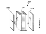
図9は、従来の一般的な液晶表示装置を示す概略分解斜視図である。 FIG. 9 is a schematic exploded perspective view showing a conventional general liquid crystal display device.
図9に示すように、従来の液晶表示装置100は、入射側の偏光板102Aと、出射側の偏光板102Bと、液晶セル104とを備えている。
As shown in FIG. 9, the conventional liquid
このうち、偏光板102A、102Bは、所定の振動方向の振動面を有する直線偏光のみを選択的に透過させるように構成されたものであり、それぞれの振動方向が相互に直角の関係になるようにクロスニコル状態で対向して配置されている。また、液晶セル104は画素に対応する多数のセルを含むものであり、偏光板102A、102Bの間に配置されている。
Among these, the polarizing
ここで、このような液晶表示装置100において、液晶セル104が、負の誘電異方性を有するネマチック液晶が封止されたVA(Vertical Alignment)方式(図中、液晶のダイレクターを点線で模式的に図示)を採用している場合を例に挙げると、入射側の偏光板102Aを透過した直線偏光は、液晶セル104のうち非駆動状態のセルの部分を透過する際に、位相シフトされずに透過し、出射側の偏光板102Bで遮断される。これに対し、液晶セル104のうち駆動状態のセルの部分を透過する際には、直線偏光が位相シフトされ、この位相シフト量に応じた量の光が出射側の偏光板102Bを透過して出射される。これにより、液晶セル104の駆動電圧を各セル毎に適宜制御することにより、出射側の偏光板102B側に所望の画像を表示することができる。なお、液晶表示装置100としては、上述したような光の透過及び遮断の態様をとるものに限らず、液晶セル104のうち非駆動状態のセルの部分から出射された光が出射側の偏光板102Bを透過して出射される一方で、駆動状態のセルの部分から出射された光が出射側の偏光板102Bで遮断されるように構成された液晶表示装置も存在している。
Here, in such a liquid
ところで、上述したようなVA方式の液晶セル104のうち非駆動状態のセルの部分を直線偏光が透過する場合を考えると、液晶セル104は複屈折性を有しており、厚さ方向の屈折率と面方向の屈折率とが異なるので、入射側の偏光板102Aを透過した直線偏光のうち液晶セル104の法線に沿って入射した光は位相シフトされずに透過するものの、入射側の偏光板102Aを透過した直線偏光のうち液晶セル104の法線から傾斜した方向に入射した光は液晶セル104を透過する際に位相差が生じて楕円偏光となる。この現象は、VA方式の液晶セル104内のあるセルが非駆動状態であるときに、液晶セル104内で垂直方向に配向した液晶分子が、正のCプレートとして作用することに起因したものである。なお、液晶セル104を透過する光(透過光)に対して生じる位相差の大きさは、液晶セル104内に封入された液晶分子の複屈折値や、液晶セル104の厚さ、透過光の波長等にも影響される。
By the way, considering the case where linearly polarized light is transmitted through the non-driven cell portion of the VA
以上の現象により、液晶セル104内のあるセルが非駆動状態であり、本来的には直線偏光がそのまま透過され、出射側の偏光板102Bで遮断されるべき場合であっても、液晶セル104の法線から傾斜した方向に出射された光の一部が出射側の偏光板102Bから洩れてしまうことになる。
Due to the above phenomenon, even when a certain cell in the
このため、上述したような従来の液晶表示装置100においては、正面から観察される画像に比べて、液晶セル104の法線から傾斜した方向から観察される画像の表示品位が悪化しやすいという問題(視角依存性の問題)がある。
For this reason, in the conventional liquid
上述したような従来の液晶表示装置100における視角依存性の問題を改善するため、現在までに様々な技術が開発されており、その一つとして、例えば特許文献1に記載されているように、コレステリック規則性の構造を有する位相差層(複屈折性を示す位相差層)を備えた位相差光学素子を用い、このような位相差光学素子を液晶セルと偏光板との間に配置することにより光学補償を行うようにした液晶表示装置が知られている。
In order to improve the problem of the viewing angle dependency in the conventional liquid
ここで、コレステリック規則性の構造を有する位相差光学素子では、λ=nav・p(p:液晶分子の螺旋構造における螺旋(ヘリカル)ピッチ、nav:螺旋軸に直交する平面内での平均屈折率)で表される選択反射波長が、例えば特許文献2に記載されているように、透過光の波長よりも小さくなるか又は大きくなるように調整している。 Here, in the retardation optical element having a cholesteric regular structure, λ = nav · p (p: helical pitch in the helical structure of liquid crystal molecules, nav: average refractive index in a plane orthogonal to the helical axis ) Is adjusted so as to be smaller or larger than the wavelength of the transmitted light, as described in Patent Document 2, for example.
上述したような位相差光学素子においては、上述した液晶セルの場合と同様に、位相差層の法線から傾斜した方向に入射する直線偏光は、位相差層を透過する際に位相差が生じて楕円偏光となる。この現象は、コレステリック規則性の構造が、負のCプレートとして作用することに起因したものである。なお、位相差層を透過する光(透過光)に対して生じる位相差の大きさは、位相差層内の液晶分子の複屈折値や、位相差層の厚さ、透過光の波長等にも影響される。 In the retardation optical element as described above, as in the case of the liquid crystal cell described above, the linearly polarized light incident in the direction inclined from the normal line of the retardation layer causes a retardation when transmitted through the retardation layer. Becomes elliptically polarized light. This phenomenon is caused by the fact that the cholesteric regular structure acts as a negative C plate. Note that the magnitude of the phase difference generated with respect to the light transmitted through the retardation layer (transmitted light) depends on the birefringence value of the liquid crystal molecules in the retardation layer, the thickness of the retardation layer, the wavelength of the transmitted light, and the like. Is also affected.
従って、上述したような位相差光学素子を用いれば、正のCプレートとして作用するVA方式の液晶セルで生じる位相差と、負のCプレートとして作用する位相差光学素子の位相差層で生じる位相差とが相殺するように、位相差光学素子の位相差層を適宜設計することにより、液晶表示装置の視角依存性の問題を大幅に改善することが可能である。 Therefore, if the phase difference optical element as described above is used, the phase difference generated in the VA liquid crystal cell acting as a positive C plate and the phase difference generated in the phase difference layer of the phase difference optical element acting as a negative C plate. By appropriately designing the phase difference layer of the phase difference optical element so as to cancel out the phase difference, it is possible to greatly improve the viewing angle dependency problem of the liquid crystal display device.
なお、このような液晶表示装置の視角依存性の問題は、例えば特許文献3に記載されているように、負のCプレートとして作用する位相差層(即ち、面方向の屈折率をNx,Ny、厚さ方向の屈折率をNzとしたときに、Nx=Ny>Nzの関係を有する位相差層)と、Aプレートとして作用する位相差層(即ち、面方向の屈折率をNx,Ny、厚さ方向の屈折率をNzとしたときに、Nx>Ny=Nzの関係を有する位相差層)とを併用すると、さらに大幅に改善することが可能である。 Note that the problem of the viewing angle dependency of such a liquid crystal display device is, for example, as described in Patent Document 3, a retardation layer that functions as a negative C plate (that is, the refractive index in the plane direction is expressed as Nx, Ny). , Where the refractive index in the thickness direction is Nz, a retardation layer having a relationship of Nx = Ny> Nz) and a retardation layer acting as an A plate (that is, the refractive index in the plane direction is Nx, Ny, When the refractive index in the thickness direction is Nz and the retardation layer having a relationship of Nx> Ny = Nz) is used in combination, further improvement can be achieved.
しかしながら、上述した従来の位相差光学素子(コレステリック規則性の構造を有し、負のCプレートとして作用する位相差層)を液晶セルと偏光板との間に配置する場合には、視覚依存性の問題は改善することができるものの、表示画像に明暗模様等が発生して、表示品位を著しく低下させることがあることが判明した。特に、上述したように、位相差光学素子において、負のCプレートとして作用する位相差層とAプレートとして作用する位相差層とを併用する場合に、表示品位の低下が顕著であることが判明した。 However, when the above-described conventional retardation optical element (retardation layer having a cholesteric regular structure and acting as a negative C plate) is disposed between the liquid crystal cell and the polarizing plate, the visual dependence Although the above problem can be improved, it has been found that a display image may have a bright and dark pattern and the display quality may be significantly reduced. In particular, as described above, in the retardation optical element, when the retardation layer that acts as a negative C plate and the retardation layer that acts as an A plate are used in combination, it is found that the display quality is significantly reduced. did.
本発明の発明者は、このような位相差光学素子(負のCプレートとして作用する位相差層とAプレートとして作用する位相差層とを備えたもの)により明暗模様等が発生する原因について実験及びコンピュータシミュレーションを用いて鋭意研究を行った結果、その原因の一つが位相差層の表面における液晶分子のダイレクターの方向にあることを突き止めた。 The inventor of the present invention conducted an experiment on the cause of the occurrence of a bright and dark pattern or the like caused by such a retardation optical element (having a retardation layer acting as a negative C plate and a retardation layer acting as an A plate). And as a result of earnest research using computer simulation, it was found that one of the causes is the direction of the director of liquid crystal molecules on the surface of the retardation layer.
なお、本発明者は既に、コレステリック規則性を有する液晶層を一つ又は複数備えた円偏光抽出光学素子において、液晶層の表面における液晶分子のダイレクターの方向や、隣接した液晶層の界面近傍の液晶分子のダイレクターの方向に関して各種の提案をしているが(特許文献4及び5)、これらの提案はあくまでもコレステリック規則性を有する単層の液晶層又は互いに積層された複数の液晶層を備えた円偏光抽出光学素子に関するものであり、上述したような位相差光学素子(負のCプレートとして作用する位相差層とAプレートとして作用する位相差層とを備えたもの)に好適な構成は必ずしも明確ではなかった。
本発明はこのような背景の下でなされたものであり、液晶セルと偏光板との間に配置した場合でも表示画像に明暗模様等を発生させることがなく、表示品位が低下してしまうことを効果的に抑制することができる、負のCプレートとして作用する位相差層とAプレートとして作用する位相差層とを含んでなる位相差光学素子、その製造方法及び位相差光学素子を備えた液晶表示装置を提供することを目的とする。 The present invention has been made under such a background, and even when it is arranged between the liquid crystal cell and the polarizing plate, the display image does not generate a bright and dark pattern and the display quality is deteriorated. A phase difference optical element comprising a phase difference layer acting as a negative C plate and a phase difference layer acting as an A plate, a method of manufacturing the same, and a phase difference optical element An object is to provide a liquid crystal display device.
本発明は、第1の解決手段として、プレーナー配向されたコレステリック規則性の構造を有し、負のCプレートとして作用するCプレート型位相差層であって、前記構造に起因した選択反射光の選択反射波長が入射光の波長と異なる範囲に存在するように前記構造の螺旋ピッチが調整されたCプレート型位相差層と、前記Cプレート型位相差層に隣接して積層され、ネマチック規則性の構造を有し、Aプレートとして作用するAプレート型位相差層とを備え、前記Cプレート型位相差層の互いに対向する2つの主たる表面のうち前記Aプレート型位相差層側の表面における液晶分子のダイレクターの方向と、前記Aプレート型位相差層の互いに対向する2つの主たる表面のうち前記Cプレート型位相差層側の表面における液晶分子のダイレクターの方向とが実質的に一致していることを特徴とする位相差光学素子を提供する。 The present invention provides, as a first solution, a C-plate type retardation layer having a planar-oriented cholesteric regular structure and acting as a negative C-plate, wherein the selectively reflected light caused by the structure is A C plate type retardation layer whose spiral pitch of the structure is adjusted so that a selective reflection wavelength is in a range different from the wavelength of incident light, and a nematic regularity are laminated adjacent to the C plate type retardation layer. Liquid crystal on the surface on the side of the A plate type retardation layer of the two main surfaces of the C plate type retardation layer facing each other. The direction of the molecular director and the directivity of the liquid crystal molecules on the surface of the A plate type retardation layer facing the C plate type retardation layer among the two main surfaces facing each other. And direction over to provide a retardation optical element, characterized in that substantially matches.
なお、上述した第1の解決手段において、前記Cプレート型位相差層の前記2つの主たる表面のうち、前記Aプレート型位相差層側の表面における液晶分子のダイレクターの方向と、前記Aプレート型位相差層から離間している側の表面における液晶分子のダイレクターの方向とが実質的に平行であることが好ましい。 In the first solving means described above, the direction of the director of liquid crystal molecules on the surface on the A plate type retardation layer side among the two main surfaces of the C plate type retardation layer, and the A plate It is preferable that the direction of the director of the liquid crystal molecules on the surface separated from the mold retardation layer is substantially parallel.
また、上述した第1の解決手段において、前記Cプレート型位相差層のうち前記Aプレート型位相差層から離間している側の表面における液晶分子のダイレクターの方向と、前記Aプレート型位相差層のうち前記Cプレート型位相差層から離間している側の表面における液晶分子のダイレクターの方向とが実質的に平行であることが好ましい。 Further, in the first solving means described above, the direction of the director of the liquid crystal molecules on the surface of the C plate type retardation layer that is separated from the A plate type retardation layer, and the A plate type position It is preferable that the direction of the director of the liquid crystal molecules on the surface of the phase difference layer that is away from the C plate type phase difference layer is substantially parallel.
さらに、上述した第1の解決手段において、前記Cプレート型位相差層の前記2つの主たる表面のうち、前記Aプレート型位相差層側の表面と、前記Aプレート型位相差層から離間している側の表面との間に、実質的に0.5×整数倍のピッチ数の螺旋構造を有することが好ましい。 Further, in the first solving means described above, of the two main surfaces of the C plate type retardation layer, the surface on the A plate type retardation layer side is separated from the A plate type retardation layer. It is preferable to have a spiral structure having a pitch number of 0.5 × integer multiple substantially between the surface and the outer surface.
さらに、上述した第1の解決手段において、前記Cプレート型位相差層は、カイラルネマチック液晶が3次元架橋されて固定化された構造、又は、高分子コレステリック液晶がガラス状に固定化された構造を有することが好ましい。 Furthermore, in the first solving means described above, the C plate type retardation layer has a structure in which chiral nematic liquid crystal is fixed by three-dimensional crosslinking, or a structure in which polymer cholesteric liquid crystal is fixed in glass. It is preferable to have.
さらに、上述した第1の解決手段において、前記Aプレート型位相差層は、ネマチック液晶が3次元架橋されて固定化された構造、又は、高分子ネマチック液晶がガラス状に固定化された構造を有することが好ましい。 Further, in the first solving means described above, the A plate type retardation layer has a structure in which nematic liquid crystal is fixed by three-dimensional crosslinking or a structure in which polymer nematic liquid crystal is fixed in a glass shape. It is preferable to have.
本発明は、第2の解決手段として、配向規制力の方向が膜上の全範囲で実質的に同一とされた配向膜上に、コレステリック規則性を有する第1液晶であって、固化時の選択反射波長が入射光の波長と異なる範囲に存在するように調整された第1液晶をコーティングする工程と、コーティングされた前記第1液晶の一方の表面における液晶分子のダイレクターの方向を前記配向膜の配向規制力によって規制した状態で固化させ、負のCプレートとして作用するCプレート型位相差層を形成する工程と、形成された前記Cプレート型位相差層上に直接、ネマチック規則性を有する第2液晶をコーティングする工程と、コーティングされた前記第2液晶の前記Cプレート型位相差層側の表面における液晶分子のダイレクターの方向を、前記Cプレート型位相差層の表面の配向規制力によって規制した状態で固化させ、Aプレートとして作用するAプレート型位相差層を形成する工程とを含むことを特徴とする、位相差光学素子の製造方法を提供する。 As a second solution, the present invention provides a first liquid crystal having cholesteric regularity on an alignment film in which the direction of alignment regulating force is substantially the same in the entire range on the film. Coating the first liquid crystal adjusted so that the selective reflection wavelength is in a range different from the wavelength of the incident light, and aligning the direction of the director of the liquid crystal molecules on one surface of the coated first liquid crystal Solidifying in a state regulated by the orientation regulating force of the film to form a C plate type retardation layer acting as a negative C plate, and nematic regularity directly on the formed C plate type retardation layer Coating the second liquid crystal, and the direction of the director of the liquid crystal molecules on the surface of the coated second liquid crystal on the side of the C plate type retardation layer. A method of manufacturing a retardation optical element, comprising: solidifying the surface of the mold retardation layer in a state regulated by the orientation regulating force of the surface of the retardation layer, and forming an A plate retardation layer acting as an A plate. provide.
なお、上述した第2の解決手段において、前記第1液晶は、コレステリック規則性を有する重合性モノマー分子及びコレステリック規則性を有する重合性オリゴマー分子のうちの少なくとも一つを含む液晶であり、当該第1液晶の一方の表面における液晶分子のダイレクターの方向が前記配向膜の配向規制力によって規制された状態で3次元架橋により固化され、前記第2液晶は、ネマチック規則性を有する重合性モノマー分子及びネマチック規則性を有する重合性オリゴマー分子のうちの少なくとも一つを含む液晶であり、当該第2液晶の前記Cプレート型位相差層側の表面における液晶分子のダイレクターの方向が前記Cプレート型位相差層の表面の配向規制力によって規制された状態で3次元架橋により固化されることが好ましい。 In the second solution described above, the first liquid crystal is a liquid crystal including at least one of a polymerizable monomer molecule having cholesteric regularity and a polymerizable oligomer molecule having cholesteric regularity. One liquid crystal is solidified by three-dimensional crosslinking in a state where the direction of director of liquid crystal molecules on one surface is regulated by the alignment regulating force of the alignment film, and the second liquid crystal is a polymerizable monomer molecule having nematic regularity. And a liquid crystal molecule including at least one of polymerizable oligomer molecules having nematic regularity, and the direction of the director of the liquid crystal molecules on the surface of the second liquid crystal on the side of the C plate type retardation layer is the C plate type. It is preferable to solidify by three-dimensional crosslinking in a state regulated by the orientation regulating force on the surface of the retardation layer.
また、上述した第2の解決手段において、前記第1液晶は、コレステリック規則性を有する液晶ポリマーを含む液晶であり、当該第1液晶の一方の表面における液晶分子のダイレクターの方向が前記配向膜の配向規制力によって規制された状態で冷却によりガラス状に固化され、前記第2液晶は、ネマチック規則性を有する液晶ポリマーを含む液晶であり、当該第2液晶の前記Cプレート型位相差層側の表面における液晶分子のダイレクターの方向が前記Cプレート型位相差層の表面の配向規制力によって規制された状態で冷却によりガラス状に固化されることが好ましい。 In the second solution described above, the first liquid crystal is a liquid crystal containing a liquid crystal polymer having cholesteric regularity, and a direction of a director of liquid crystal molecules on one surface of the first liquid crystal is the alignment film. The second liquid crystal is a liquid crystal containing a liquid crystal polymer having nematic regularity, and is solidified into a glass shape by cooling in a state regulated by the alignment regulating force of the second liquid crystal, and on the C plate type retardation layer side of the second liquid crystal It is preferable that the direction of the director of the liquid crystal molecules on the surface is solidified into glass by cooling in a state in which the direction is regulated by the alignment regulating force on the surface of the C plate type retardation layer.
ここで、上述した第2の解決手段において、前記Cプレート型位相差層の互いに対向する2つの主たる表面の両方における液晶分子のダイレクターの方向が実質的に平行となるように、前記第1液晶のコーティングの厚さを調整することが好ましい。 Here, in the second solving means described above, the first liquid crystal molecule directors on both of the two main surfaces facing each other of the C plate type retardation layer are substantially parallel to each other. It is preferable to adjust the thickness of the liquid crystal coating.
また、上述した第2の解決手段において、前記Cプレート型位相差層の互いに対向する2つの主たる表面の両方における液晶分子のダイレクターの方向を規制した状態で前記液晶を固化させるように、前記配向膜の表面から離間している側の表面に他の配向膜を当接させることが好ましい。 In the second solution described above, the liquid crystal is solidified in a state where the directions of the directors of the liquid crystal molecules on both of the two main surfaces facing each other of the C plate type retardation layer are regulated. It is preferable that another alignment film is brought into contact with the surface on the side away from the surface of the alignment film.
さらに、上述した第2の解決手段において、前記Aプレート型位相差層の互いに対向する2つの主たる表面の両方における液晶分子のダイレクターの方向を規制した状態で前記液晶を固化させるように、前記Cプレート型位相差層の表面から離間している側の表面に他の配向膜を当接させることが好ましい。 Furthermore, in the second solution described above, the liquid crystal is solidified in a state where the directions of the directors of the liquid crystal molecules on both of the two main surfaces facing each other of the A plate type retardation layer are regulated. It is preferable that another alignment film is brought into contact with the surface on the side away from the surface of the C plate type retardation layer.
本発明は、第3の解決手段として、配向規制力の方向が膜上の全範囲で実質的に同一とされた配向膜上に、ネマチック規則性を有する第1液晶をコーティングする工程と、コーティングされた前記第1液晶の一方の表面における液晶分子のダイレクターの方向を前記配向膜の配向規制力によって規制した状態で固化させ、Aプレートとして作用するAプレート型位相差層を形成する工程と、形成された前記Aプレート型位相差層上に直接、コレステリック規則性を有する第2液晶であって、固化時の選択反射波長が入射光の波長と異なる範囲に存在するように調整された第2液晶をコーティングする工程と、コーティングされた前記第2液晶の前記Aプレート型位相差層側の表面における液晶分子のダイレクターの方向を、前記Aプレート型位相差層の表面の配向規制力によって規制した状態で固化させ、負のCプレートとして作用するCプレート型位相差層を形成する工程とを含むことを特徴とする、位相差光学素子の製造方法を提供する。 The present invention provides, as a third solution, a step of coating a first liquid crystal having nematic regularity on an alignment film in which the direction of alignment regulating force is substantially the same over the entire range, Solidifying the direction of the director of the liquid crystal molecules on one surface of the first liquid crystal, which is regulated by the alignment regulating force of the alignment film, to form an A plate type retardation layer acting as an A plate; The second liquid crystal having cholesteric regularity directly on the formed A-plate type retardation layer, and adjusted so that the selective reflection wavelength when solidified is in a range different from the wavelength of incident light. The step of coating two liquid crystals, and the direction of the director of the liquid crystal molecules on the surface of the coated second liquid crystal on the side of the A plate type retardation layer. And a step of solidifying the surface of the phase difference layer in a state regulated by the orientation regulating force of the phase difference layer to form a C plate type phase difference layer that acts as a negative C plate. provide.
なお、上述した第3の解決手段において、前記第1液晶は、ネマチック規則性を有する重合性モノマー分子及びネマチック規則性を有する重合性オリゴマー分子のうちの少なくとも一つを含む液晶であり、当該第1液晶の一方の表面における液晶分子のダイレクターの方向が前記配向膜の配向規制力によって規制された状態で3次元架橋により固化され、前記第2液晶は、コレステリック規則性を有する重合性モノマー分子及びコレステリック規則性を有する重合性オリゴマー分子のうちの少なくとも一つを含む液晶であり、当該第2液晶の前記Aプレート型位相差層側の表面における液晶分子のダイレクターの方向が前記Aプレート型位相差層の表面の配向規制力によって規制された状態で3次元架橋により固化されることが好ましい。 In the third solution described above, the first liquid crystal is a liquid crystal including at least one of a polymerizable monomer molecule having a nematic regularity and a polymerizable oligomer molecule having a nematic regularity. One liquid crystal is solidified by three-dimensional crosslinking in a state where the direction of the director of the liquid crystal molecules on one surface is regulated by the alignment regulating force of the alignment film, and the second liquid crystal is a polymerizable monomer molecule having cholesteric regularity And a liquid crystal molecule containing at least one of polymerizable oligomer molecules having cholesteric regularity, and the direction of the director of the liquid crystal molecules on the surface of the second liquid crystal on the side of the A plate type retardation layer is the A plate type. It is preferable to solidify by three-dimensional crosslinking in a state regulated by the orientation regulating force on the surface of the retardation layer.
また、上述した第3の解決手段において、前記第1液晶は、ネマチック規則性を有する液晶ポリマーを含む液晶であり、当該第1液晶の一方の表面における液晶分子のダイレクターの方向が前記配向膜の配向規制力によって規制された状態で冷却によりガラス状に固化され、前記第2液晶は、コレステリック規則性を有する液晶ポリマーを含む液晶であり、当該第2液晶の前記Aプレート型位相差層側の表面における液晶分子のダイレクターの方向が前記Aプレート型位相差層の表面の配向規制力によって規制された状態で冷却によりガラス状に固化されることが好ましい。 In the third solution described above, the first liquid crystal is a liquid crystal containing a liquid crystal polymer having nematic regularity, and a direction of a director of liquid crystal molecules on one surface of the first liquid crystal is the alignment film. The second liquid crystal is a liquid crystal containing a liquid crystal polymer having cholesteric regularity, and is solidified into a glass shape by cooling in a state regulated by the alignment regulating force of the second liquid crystal, and on the A plate type retardation layer side of the second liquid crystal It is preferable that the direction of the director of the liquid crystal molecules on the surface of the liquid crystal is solidified into glass by cooling in a state in which the direction is regulated by the alignment regulating force on the surface of the A plate type retardation layer.
ここで、上述した第3の解決手段において、前記Cプレート型位相差層の互いに対向する2つの主たる表面の両方における液晶分子のダイレクターの方向が実質的に平行となるように、前記第2液晶のコーティングの厚さを調整することが好ましい。 Here, in the third solving means described above, the direction of the director of the liquid crystal molecules on both of the two main surfaces facing each other of the C plate type retardation layer is substantially parallel. It is preferable to adjust the thickness of the liquid crystal coating.
また、上述した第3の解決手段において、前記Cプレート型位相差層の互いに対向する2つの主たる表面の両方における液晶分子のダイレクターの方向を規制した状態で前記第2液晶を固化させるように、前記Aプレート型位相差層の表面から離間している側の表面に他の配向膜を当接させることが好ましい。 In the third solution described above, the second liquid crystal is solidified in a state where the directions of the directors of the liquid crystal molecules on both of the two main surfaces of the C plate type retardation layer facing each other are regulated. It is preferable that another alignment film is brought into contact with the surface on the side away from the surface of the A plate type retardation layer.
さらに、上述した第3の解決手段において、前記Aプレート型位相差層の互いに対向する2つの主たる表面の両方における液晶分子のダイレクターの方向を規制した状態で前記第2液晶を固化させるように、前記配向膜の表面から離間している側の表面に他の配向膜を当接させることが好ましい。 Furthermore, in the third solution described above, the second liquid crystal is solidified in a state where the directions of the directors of the liquid crystal molecules on both of the two main surfaces facing each other of the A plate type retardation layer are regulated. It is preferable that another alignment film is brought into contact with the surface on the side away from the surface of the alignment film.
本発明は、第4の解決手段として、液晶セルと、前記液晶セルを挟むように配置された一対の偏光板と、前記液晶セルと前記一対の偏光板の少なくとも一方との間に配置された、上述した第1の解決手段に係る位相差光学素子とを備え、前記位相差光学素子は、前記液晶セルへ入射及び/又は前記液晶セルから出射された所定の偏光状態の光のうち当該液晶セルの法線から傾斜した方向に出射される光の偏光状態を補償することを特徴とする液晶表示装置を提供する。 As a fourth solution, the present invention is arranged between a liquid crystal cell, a pair of polarizing plates arranged so as to sandwich the liquid crystal cell, and at least one of the liquid crystal cell and the pair of polarizing plates. The phase difference optical element according to the first solving means described above, wherein the phase difference optical element is a liquid crystal of light in a predetermined polarization state incident on and / or emitted from the liquid crystal cell. Provided is a liquid crystal display device that compensates for a polarization state of light emitted in a direction inclined from a normal line of a cell.
本発明の第1の解決手段に係る位相差光学素子によれば、プレーナー配向されたコレステリック規則性の構造を有し、負のCプレートとして作用するCプレート型位相差層に、ネマチック規則性の構造を有し、Aプレートとして作用するAプレート型位相差層を隣接して積層した位相差光学素子において、Cプレート型位相差層の構造に起因した選択反射光の選択反射波長が入射光の波長と異なる範囲に存在するように前記構造の螺旋ピッチを調整し、且つ、Cプレート型位相差層及びAプレート型位相差層の互いに隣接する側の表面における液晶分子のダイレクターの方向を実質的に一致させるようにしているので、液晶セルと偏光板との間に配置した場合でも表示画像に明暗模様等を発生させることがなく、表示品位が低下してしまうことを効果的に抑制することができる。 According to the retardation optical element according to the first solution of the present invention, the nematic regularity is applied to the C-plate type retardation layer having a planar-oriented cholesteric regular structure and acting as a negative C plate. In a phase difference optical element having an A plate type retardation layer having a structure and acting as an A plate adjacent to each other, the selective reflection wavelength of the selective reflection light caused by the structure of the C plate type retardation layer is The spiral pitch of the structure is adjusted so that it exists in a range different from the wavelength, and the direction of the director of the liquid crystal molecules on the surfaces adjacent to each other of the C plate type retardation layer and the A plate type retardation layer is substantially Therefore, even if it is placed between the liquid crystal cell and the polarizing plate, the display image does not generate a bright and dark pattern, and the display quality deteriorates. It can be effectively suppressed.
ここで、本発明の第1の解決手段に係る位相差光学素子においては、Cプレート型位相差層の2つの主たる表面における液晶分子のダイレクターの方向が実質的に平行であるようにすることにより、明暗模様等の発生をより効果的に抑制して、表示品位の低下をさらに抑制することができる。 Here, in the retardation optical element according to the first solving means of the present invention, the directions of the directors of the liquid crystal molecules on the two main surfaces of the C-plate retardation layer are substantially parallel. Thus, it is possible to more effectively suppress the occurrence of bright and dark patterns and further suppress the deterioration of display quality.
また、本発明の第1の解決手段に係る位相差光学素子においては、互いに隣接して積層されたCプレート型位相差層及びAプレート型位相差層の互いに離間する2つの主たる表面における液晶分子のダイレクターの方向が実質的に平行であるようにすることにより、明暗模様等の発生をさらに効果的に抑制することができる。 In the retardation optical element according to the first solving means of the present invention, the liquid crystal molecules on the two main surfaces of the C plate type retardation layer and the A plate type retardation layer that are stacked adjacent to each other are separated from each other. By making the directions of the directors substantially parallel to each other, it is possible to more effectively suppress the occurrence of bright and dark patterns.
さらに、本発明の第1の解決手段に係る位相差光学素子においては、Cプレート型位相差層の2つの主たる表面の間に、実質的に0.5×整数倍のピッチ数の螺旋構造を有するようにすることにより、Cプレート型位相差層の2つの主たる表面における液晶分子のダイレクターの方向を正確に一致させることができ、これにより、明暗模様等の発生をより効果的に抑制して、表示品位の低下をさらに抑制することができる。 Furthermore, in the phase difference optical element according to the first solving means of the present invention, a spiral structure having a pitch number substantially 0.5 × integer multiple is provided between two main surfaces of the C plate type phase difference layer. By having it, the directions of the directors of the liquid crystal molecules on the two main surfaces of the C-plate type retardation layer can be made to coincide with each other, thereby suppressing the occurrence of bright and dark patterns more effectively. Thus, it is possible to further suppress the deterioration of display quality.
本発明の第2の解決手段に係る位相差光学素子の製造方法によれば、配向規制力の方向が膜上の全範囲で実質的に同一とされた配向膜上に、コレステリック規則性を有する第1液晶をコーティングして、負のCプレートとして作用するCプレート型位相差層を形成し、次いで、この形成されたCプレート型位相差層上に直接、ネマチック規則性を有する第2液晶をコーティングして、Aプレートとして作用するAプレート型位相差層を形成しているので、負のCプレートとして作用する位相差層とAプレートとして作用する位相差層とを含んでなる位相差光学素子であって、表示画像に明暗模様を発生させることがなく、且つ、表示品位が低下してしまうことを効果的に抑制することができる位相差光学素子を容易に製造することができる。 According to the method of manufacturing a retardation optical element according to the second solution of the present invention, the alignment film has cholesteric regularity on the alignment film in which the direction of the alignment control force is substantially the same over the entire range. The first liquid crystal is coated to form a C plate type retardation layer that acts as a negative C plate, and then a second liquid crystal having nematic regularity is directly formed on the formed C plate type retardation layer. Since the A plate type retardation layer acting as an A plate is formed by coating, a retardation optical element comprising a retardation layer acting as a negative C plate and a retardation layer acting as an A plate In addition, it is possible to easily manufacture a phase difference optical element that does not generate a bright and dark pattern in a display image and can effectively suppress deterioration in display quality.
本発明の第3の解決手段に係る位相差光学素子の製造方法によれば、配向規制力の方向が膜上の全範囲で実質的に同一とされた配向膜上に、ネマチック規則性を有する第1液晶をコーティングして、Aプレートとして作用するAプレート型位相差層を形成し、次いで、この形成されたAプレート型位相差層上に直接、コレステリック規則性を有する第2液晶をコーティングして、負のCプレートとして作用するCプレート型位相差層を形成しているので、負のCプレートとして作用する位相差層とAプレートとして作用する位相差層とを含んでなる位相差光学素子であって、表示画像に明暗模様を発生させることがなく、且つ、表示品位が低下してしまうことを効果的に抑制することができる位相差光学素子を容易に製造することができる。 According to the method for manufacturing a retardation optical element according to the third solution of the present invention, nematic regularity is provided on the alignment film in which the direction of the alignment control force is substantially the same in the entire range on the film. A first liquid crystal is coated to form an A plate type retardation layer that acts as an A plate, and then a second liquid crystal having cholesteric regularity is directly coated on the formed A plate type retardation layer. Since the C plate type retardation layer acting as the negative C plate is formed, the retardation optical element comprising the retardation layer acting as the negative C plate and the retardation layer acting as the A plate In addition, it is possible to easily manufacture a phase difference optical element that does not generate a bright and dark pattern in a display image and can effectively suppress deterioration in display quality.
本発明の第4の解決手段によれば、液晶表示装置の液晶セルと偏光板との間に位相差光学素子を配置し、液晶セルへ入射及び/又は液晶セルから出射された所定の偏光状態の光のうち当該液晶セルの法線から傾斜した方向に出射される光の偏光状態を補償するので、液晶表示装置における明暗模様の発生を抑制するとともにコントラストを向上させることができ、表示品位の低下を抑制することができる。 According to the fourth solution of the present invention, a retardation optical element is disposed between the liquid crystal cell and the polarizing plate of the liquid crystal display device, and a predetermined polarization state incident on and / or emitted from the liquid crystal cell. Compensation of the polarization state of the light emitted in the direction inclined from the normal line of the liquid crystal cell, thereby suppressing the occurrence of bright and dark patterns in the liquid crystal display device and improving the contrast. The decrease can be suppressed.
以下、図面を参照して本発明の実施の形態について説明する。 Embodiments of the present invention will be described below with reference to the drawings.
まず、図1により、本実施の形態に係る位相差光学素子について説明する。 First, the retardation optical element according to the present embodiment will be described with reference to FIG.
図1に示されるように、位相差光学素子10は、プレーナー配向されたコレステリック規則性の構造を有するCプレート型位相差層12と、Cプレート型位相差層12に隣接して積層され、ネマチック規則性の構造を有するAプレート型位相差層14とを備えている。
As shown in FIG. 1, a retardation
このうち、Cプレート型位相差層12は、厚さ方向(法線15の方向)に直交するように配置された互いに対向する2つの主たる表面(広い方の表面)12A、12Bを有している。なお、Cプレート型位相差層12は、コレステリック規則性の構造に起因して異方性、即ち複屈折性を有し、厚さ方向の屈折率と面方向の屈折率とが異なるので、負のCプレートとして作用する。即ち、3次元直交座標系で、Cプレート型位相差層12の面方向の屈折率をNx、Ny、厚さ方向の屈折率をNzとすると、Nx=Ny>Nzの関係となっている。
Among these, the C plate
また、Aプレート型位相差層14は、厚さ方向(法線15の方向)に直交するように配置された互いに対向する2つの主たる表面(広い方の表面)14A、14Bを有している。なお、Aプレート型位相差層12は、ネマチック規則性の構造に起因して異方性、即ち複屈折性を有し、面方向の屈折率が異なるので、(正の)Aプレートとして作用する。即ち、3次元直交座標系で、Aプレート型位相差層14の面方向の屈折率をNx、Ny、厚さ方向の屈折率をNzとすると、Nx>Ny=Nzの関係となっている。
Further, the A plate
ここで、Cプレート型位相差層12のうちAプレート型位相差層14側の表面12Bにおける液晶分子のダイレクターCbの方向と、Aプレート型位相差層14のうちCプレート型位相差層12側の表面14Aにおける液晶分子のダイレクターNaの方向とが実質的に一致している。なお、Cプレート型位相差層12の表面12Bにおける液晶分子のダイレクターCbの方向とAプレート型位相差層14の表面14Aにおける液晶分子のダイレクターの方向のばらつきの範囲は、±10°以内、好ましく±5°以内、さらに好ましくは±1°以内である。
Here, the direction of the liquid crystal molecule director Cb on the
なお、ここでいう「実質的に一致する」とは、液晶分子のダイレクターの方向がほぼ180度ずれている場合、即ち液晶分子の頭及び尻が同一の方向にある場合も含むものである。これは、多くの場合、液晶分子の頭と尻とを光学的に区別することができないからである。なお、この関係は、後述する場合(Cプレート型位相差層12の2つの主たる表面12A、12Bにおける液晶分子のダイレクターCa、Cbの方向が「実質的に平行である」場合や、Cプレート型位相差層12及びAプレート型位相差層14の互いに離間する2つの表面12A、14Bにおける液晶分子のダイレクターCa、Nbの方向が「実質的に平行である」場合)も同様である。
Here, “substantially coincide” includes the case where the direction of the director of the liquid crystal molecules is shifted by approximately 180 degrees, that is, the case where the head and the bottom of the liquid crystal molecules are in the same direction. This is because in many cases, the head and the bottom of the liquid crystal molecules cannot be optically distinguished. This relationship is described later (when the directions of the directors Ca and Cb of the liquid crystal molecules on the two
また、「液晶分子」という用語は、一般的には液体の流動性と結晶の異方性とを兼ね備えた分子という意味で用いられるが、本明細書においては、流動性を有する状態で有していた異方性を保持しつつ固化された分子についても便宜上、「液晶分子」という用語を用いることとする。分子が流動性を有する状態で有していた異方性を保持しつつ固化させる方法としては、例えば、重合可能な基を有する液晶性分子(重合性モノマー分子又は重合性オリゴマー分子)を架橋させる方法や、高分子液晶(液晶ポリマー)をガラス転移温度以下に冷却する方法等がある。 In addition, the term “liquid crystal molecule” is generally used to mean a molecule having both fluidity of liquid and crystal anisotropy. For the sake of convenience, the term “liquid crystal molecule” is also used for molecules that have been solidified while maintaining the anisotropy. As a method of solidifying while maintaining the anisotropy that the molecule has in the fluid state, for example, a liquid crystal molecule (polymerizable monomer molecule or polymerizable oligomer molecule) having a polymerizable group is crosslinked. And a method of cooling a polymer liquid crystal (liquid crystal polymer) to a glass transition temperature or lower.
なお、Cプレート型位相差層12の2つの主たる表面のうち、一方の表面12Aにおける液晶分子のダイレクターCaの方向はその面内で実質的に一致しており、他方の表面12Bにおける液晶分子のダイレクターCbの方向もその面内で実質的に一致していることが好ましい。なお、Cプレート型位相差層12の一方の表面12A及び他方の表面12Bにおける液晶分子のダイレクターCa、Cbの方向のばらつきの範囲は、±10°以内、好ましく±5°以内、さらに好ましくは±1°以内であることが好ましい。
Of the two main surfaces of the C-plate
ここで、Cプレート型位相差層12の表面12A、12Bにおいて、液晶分子のダイレクターCa、Cbの方向が実質的に一致しているか否かは、Cプレート型位相差層12の断面を透過型電子顕微鏡で観察することによって判別することができる。詳細には、透過型電子顕微鏡により、コレステリック規則性の液晶構造のまま固化されたCプレート型位相差層12の断面を観察すると、コレステリック規則性の液晶構造特有の、分子の螺旋ピッチに相当する明暗模様が観察される。従って、このとき、各表面12A、12Bにおいて、面に沿って明暗の濃度にばらつきがなくほぼ同程度に見えれば、この面内の液晶分子のダイレクターの方向が実質的に一致しているものと判断することができる。
Here, whether or not the directions of the directors Ca and Cb of the liquid crystal molecules substantially coincide on the
なお、図1に示す位相差光学素子10において、コレステリック規則性の構造を有し、負のCプレートとして作用するCプレート型位相差層12は、複屈折性を有しており、厚さ方向の屈折率と面方向の屈折率とが異なっている。従って、Cプレート型位相差層12に直線偏光が入射する場合には、Cプレート型位相差層12の法線15の方向に入射した直線偏光は位相シフトされずに透過されるものの、Cプレート型位相差層12の法線15から傾斜した方向に入射した直線偏光はCプレート型位相差層12を透過する際に位相差が生じて楕円偏光となる。なお逆に、Cプレート型位相差層12の法線15から傾斜した方向に楕円偏光が入射した場合には、入射した楕円偏光を直線偏光にすることも可能である。
In the retardation
これに対し、ネマチック規則性の構造を有し、Aプレートとして作用するAプレート型位相差層14も複屈折性を有しているが、面方向の屈折率が異なっている。即ち、表面14A、14Bに沿った方向でも、ダイレクターNa、Nbの方向の屈折率と、ダイレクターNa、Nbに垂直な方向の屈折率とが異なる。なお、ダイレクターNa、Nbに垂直な方向の屈折率と、厚さ方向の屈折率とは等しい。
On the other hand, the A plate
従って、このような、複屈折の態様が方向的に異なる2種類の位相差層(Cプレート型位相差層12及びAプレート型位相差層14)を併用して位相差光学素子を構成することにより、法線15の方向に透過する光及び法線15から傾斜した方向に透過する光の双方に対して位相シフト作用を施すことができ、多様な光学的補償を実現することができる。
Therefore, a phase difference optical element is configured by using two types of retardation layers (C plate
なおこのとき、Cプレート型位相差層12及びAプレート型位相差層14が互いに隣接して積層され、且つ、Cプレート型位相差層12及びAプレート型位相差層14の互いに隣接する側の表面12B、14Aにおける液晶分子のダイレクターCb、Naの方向が実質的に一致しているので、液晶表示装置の液晶セルと偏光板との間に配置した場合でも表示画像に明暗模様等を発生させることがなく、表示品位が低下してしまうことを効果的に抑制することができる。
At this time, the C plate
なお、Cプレート型位相差層12においては、コレステリック規則性の構造に起因した選択反射光の選択反射波長が入射光の波長と異なる範囲(選択反射波長が入射光の波長よりも小さくなるか又は大きくなる範囲)に存在するように構造の螺旋ピッチが調整されている。これにより、例えば入射光が可視光線であるような場合であっても、液晶分子の螺旋構造による選択反射によって入射光(可視光線)が反射されることがなく、着色等の問題が生じない。
In the C-plate
ここで、コレステリック規則性の構造を有するCプレート型位相差層12における選択反射の現象について簡単に説明しておく。
Here, the phenomenon of selective reflection in the C-plate
コレステリック規則性の構造は一般的に、液晶のプレーナー配列に基づいて、一方向の旋光成分(円偏光成分)と、これと逆回りの旋光成分とを分離する旋光選択特性(偏光分離特性)を有している。 A cholesteric regular structure generally has an optical rotation selection characteristic (polarization separation characteristic) that separates an optical rotation component in one direction (circular polarization component) and an optical rotation component in the opposite direction based on the planar arrangement of the liquid crystal. Have.
このような現象は、円偏光二色性として知られ、液晶分子の螺旋構造における旋回方向を適宜選択すると、この旋回方向と同一の旋光方向を有する円偏光成分が選択的に反射される。 Such a phenomenon is known as circular dichroism, and when a rotation direction in the helical structure of liquid crystal molecules is appropriately selected, a circularly polarized component having the same optical rotation direction as that of the rotation direction is selectively reflected.
この場合の最大旋光偏光光散乱(選択反射のピーク)は、次式(1)の選択反射波長λ0で生じる。 In this case, the maximum optical polarization polarization light scattering (selective reflection peak) occurs at the selective reflection wavelength λ 0 of the following equation (1).
λ0=nav・p … (1)
ここで、pは液晶分子の螺旋構造における螺旋ピッチ、navは螺旋軸に直交する平面内の平均屈折率である。
λ0 = nav · p (1)
Here, p is a helical pitch in the helical structure of liquid crystal molecules, and nav is an average refractive index in a plane perpendicular to the helical axis.
一方、このときの選択反射光の波長バンド幅Δλは、次式(2)で表される。 On the other hand, the wavelength bandwidth Δλ of the selectively reflected light at this time is expressed by the following equation (2).
Δλ=Δn・p … (2)
ここで、Δnは常光に対する屈折率と異常光に対する屈折率との差として表される複屈折値である。
Δλ = Δn · p (2)
Here, Δn is a birefringence value expressed as a difference between the refractive index for ordinary light and the refractive index for extraordinary light.
即ち、このようなコレステリック規則性の構造において、入射した無偏光は、上述したような偏光分離特性に従って、選択反射波長λ0を中心とした波長バンド幅△λの範囲の光の右旋又は左旋の円偏光成分の一方が反射され、他方の円偏光成分及び選択反射波長以外の他の波長領域の光(無偏光)が透過される。なお、反射された右旋又は左旋の円偏光成分は、通常の反射とは異なり、旋回方向が反転されることなく反射される。 That is, in such a cholesteric regular structure, incident non-polarized light is right-handed or left-handed in the range of the wavelength bandwidth Δλ centered on the selective reflection wavelength λ0 according to the polarization separation characteristic as described above. One of the circularly polarized components is reflected, and light (non-polarized light) in a wavelength region other than the other circularly polarized component and the selective reflection wavelength is transmitted. The reflected right-handed or left-handed circularly polarized light component is reflected without reversing the turning direction, unlike normal reflection.
ここで、着色が問題となる可視光線の波長バンド幅は380〜780nmであるので、コレステリック規則性の構造に起因した選択反射光の選択反射波長が380nm以下か又は780nm以上であるようにコレステリック規則性の構造を構成するとよい。これにより、Cプレート型位相差層12に負のCプレートとしての作用を発現させながら、入射光(可視光線)を反射してしまうことによる着色等の問題を防止することができる。なお、選択反射光の選択反射波長が入射光の波長よりも小さい場合には、旋光作用が小さくなるので、より好ましい。
Here, since the wavelength bandwidth of visible light that causes coloring is 380 to 780 nm, the cholesteric rule is such that the selective reflection wavelength of the selectively reflected light due to the structure of the cholesteric regularity is 380 nm or less or 780 nm or more. It is good to constitute a sex structure. Thereby, problems such as coloring due to reflection of incident light (visible light) can be prevented while causing the C plate-
次に、図2により、本実施の形態に係る位相差光学素子の変形例について説明する。 Next, a modification of the retardation optical element according to the present embodiment will be described with reference to FIG.
図2に示されるように、位相差光学素子20は、プレーナー配向されたコレステリック規則性の構造を有するCプレート型位相差層22と、Cプレート型位相差層22に隣接して積層され、ネマチック規則性の構造を有するAプレート型位相差層14とを備えている。
As shown in FIG. 2, the retardation
このうち、Cプレート型位相差層22は、図1に示す位相差光学素子10のCプレート型位相差層12と同様に負のCプレートとして作用するものであり、厚さ方向(法線15の方向)に直交するように配置された互いに対向する2つの主たる表面(広い方の表面)22A、22Bを有している。
Among them, the C plate
ここで、Cプレート型位相差層22の2つの主たる表面22A、22Bのうち、Aプレート型位相差層14側の表面22Bにおける液晶分子のダイレクターCbの方向と、Aプレート型位相差層14から離間している側の表面22Aにおける液晶分子のダイレクターCaの方向とは実質的に平行である。なお、Cプレート型位相差層22の一方の表面22Bにおける液晶分子のダイレクターCbの方向(平均方向)と他方の表面22Aにおける液晶分子のダイレクターCaの方向(平均方向)とがなす角度は±10°以内、好ましく±5°以内、さらに好ましくは±1°以内であることが好ましい。
Here, of the two
また、Cプレート型位相差層22のうちAプレート型位相差層14から離間している側の表面22Aにおける液晶分子のダイレクターCaの方向と、Aプレート型位相差層14のうちCプレート型位相差層22から離間している側の表面14Bにおける液晶分子のダイレクターNbの方向とは実質的に平行である。なお、Cプレート型位相差層22の表面22Aにおける液晶分子のダイレクターCaの方向(平均方向)とAプレート型位相差層14の表面14Bにおける液晶分子のダイレクターNbの方向(平均方向)とがなす角度は±10°以内、好ましく±5°以内、さらに好ましくは±1°以内であることが好ましい。
The direction of the director Ca of the liquid crystal molecules on the
ここで、図2に示す位相差光学素子20においては、Cプレート型位相差層22の2つの主たる表面22A、22Bにおける液晶分子のダイレクターCa、Cbの方向を正確に一致(即ち平行に)させるため、Cプレート型位相差層22の厚さを、コレステリック規則性の構造(螺旋構造)の螺旋ピッチpの0.5×整数倍とし、表面22A、22Bの間に、実質的に0.5×整数倍のピッチ数の螺旋構造が形成されるようにするとよい。このようにすることにより、例えば図3(A)〜(C)に模式的に示されるように、光学的に、液晶分子のコレステリック規則性の螺旋ピッチpの半分の距離で厚さが割り切れることとなり、単純化された理論式である上式(1)からの光学的なズレ、特に螺旋軸に沿って入射する入射光に対する位相シフト差による偏光状態の乱れが抑制される。
Here, in the phase difference
なお、図2に示す位相差光学素子20は、負のCプレートとして作用するCプレート型位相差層の構成が異なる点を除いて、他は、図1に示す位相差光学素子10の構成と略同一であるので、その他の構成についての詳細な説明は省略する。
2 is the same as the configuration of the phase difference
ここで、位相差光学素子10、20のCプレート型位相差層12、22及びAプレート型位相差層14の材料としては、3次元架橋可能な液晶性モノマー又は液晶性オリゴマー(重合性モノマー分子又は重合性オリゴマー分子)を用いることができる他、冷却によりガラス状に固化することが可能な高分子液晶(液晶ポリマー)を用いることもできる。
Here, as materials for the C plate type retardation layers 12 and 22 and the A plate
このうち、Cプレート型位相差層12、22及びAプレート型位相差層14の材料として、3次元架橋可能な重合性モノマー分子を用いる場合は、特開平7−258638号公報や特表平10−508882号公報に開示されているような、液晶性モノマー及びキラル化合物の混合物を用いることができる。また、3次元架橋可能な重合性オリゴマー分子を用いる場合は、特開昭57−165480号公報に開示されているようなコレステリック相を有する環式オルガノポリシロキサン化合物等が望ましい。なお、「3次元架橋」とは、重合性モノマー分子又は重合性オリゴマー分子を互いに3次元的に重合して、網目(ネットワーク)構造の状態にすることを意味する。このような状態にすることにより、液晶分子をコレステリック規則性の構造又はネマチック規則性の構造のままで光学的に固定化することができ、光学膜としての取り扱いが容易な、常温で安定したフィルム状の膜とすることができる。
Among these, when a polymerizable monomer molecule capable of three-dimensional crosslinking is used as a material for the C plate type retardation layers 12 and 22 and the A plate
ここで、3次元架橋可能な重合性モノマー分子を用いる場合を例に挙げると、液晶性モノマーを所定の温度で液晶相にするとネマチック液晶になる。また、この液晶性モノマーにカイラル剤を添加することによりカイラルネマチック液晶(コレステリック液晶)が得られる。より具体的な例を示すと、例えば一般式(1)〜(11)に示されるような液晶性モノマーを用いることができる。なお、一般式(11)で示される液晶性モノマーの場合には、Xは2〜5(整数)であることが好ましい。 Here, for example, when a polymerizable monomer molecule capable of three-dimensional crosslinking is used, a nematic liquid crystal is obtained when the liquid crystalline monomer is converted into a liquid crystal phase at a predetermined temperature. Further, a chiral nematic liquid crystal (cholesteric liquid crystal) can be obtained by adding a chiral agent to the liquid crystalline monomer. As a more specific example, for example, liquid crystalline monomers as represented by the general formulas (1) to (11) can be used. In the case of the liquid crystalline monomer represented by the general formula (11), X is preferably 2 to 5 (integer).

また、カイラル剤としては、例えば一般式(12)〜(14)に示されるようなカイラル剤を用いることが好ましい。なお、一般式(12)、(13)で示されるカイラル剤の場合、Xは2〜12(整数)であることが好ましく、また、一般式(14)で示されるカイラル剤の場合、Xは2〜5(整数)であることが好ましい。なお、一般化式(12)において、R4は水素又はメチル基を示す。 Moreover, as a chiral agent, it is preferable to use a chiral agent as shown, for example by General formula (12)-(14). In the case of the chiral agent represented by the general formulas (12) and (13), X is preferably 2 to 12 (integer), and in the case of the chiral agent represented by the general formula (14), X is It is preferable that it is 2-5 (integer). In the general formula (12), R 4 represents hydrogen or a methyl group.
一方、Cプレート型位相差層12、22及びAプレート型位相差層14の材料として、液晶ポリマーを用いる場合には、液晶を呈するメソゲン基を主鎖、側鎖、あるいは主鎖及び側鎖の両方の位置に導入した高分子、コレステリル基を側鎖に導入した高分子コレステリック液晶、特開平9−133810号公報に開示されているような液晶性高分子、特開平11−293252号公報に開示されているような液晶性高分子等を用いることができる。
On the other hand, when a liquid crystal polymer is used as the material of the C plate type retardation layers 12 and 22 and the A plate
次に、このような構成からなる本実施の形態に係る位相差光学素子10(20)の製造方法について説明する。 Next, a method for manufacturing the retardation optical element 10 (20) according to the present embodiment having such a configuration will be described.
(第1の製造方法)
まず、図4(A)〜(E)により、Cプレート型位相差層12(22)及びAプレート型位相差層14の材料として、重合性モノマー分子又は重合性オリゴマー分子を用いる場合の製造方法について説明する。
(First manufacturing method)
First, referring to FIGS. 4A to 4E, a manufacturing method in the case of using a polymerizable monomer molecule or a polymerizable oligomer molecule as a material of the C plate type retardation layer 12 (22) and the A plate
(1) Cプレート型位相差層の形成
この場合には、図4(A)に示されるように、ガラス基板又はTAC(三酢酸セルロース)フィルム等の高分子フィルム16上に配向膜17を形成しておき、その上に、図4(B)に示されるように、コレステリック規則性を有する重合性モノマー分子(又は重合性オリゴマー分子)18をコーティングし、配向膜17の配向規制力によって配向させる。このとき、コーティングされた重合性モノマー分子(又は重合性オリゴマー分子)18は液晶層を構成している。
(1) Formation of C plate type retardation layer In this case, as shown in FIG. 4A, an
なお、重合性モノマー分子(又は重合性オリゴマー分子)18を所定の温度で液晶層にした場合には、ネマチック液晶になるが、ここに任意のカイラル剤を添加すれば、カイラルネマチック液晶(コレステリック液晶)となる。具体的には例えば、重合性モノマー分子又は重合性オリゴマー分子に、カイラル剤を数%〜10%程度入れるとよい。なお、カイラル剤の種類を変えてカイラルパワーを変えるか、あるいは、カイラル剤の濃度を変化させることにより、重合性モノマー分子又は重合性オリゴマー分子の分子構造に起因する選択反射波長を制御することができる。なお、重合性モノマー分子(又は重合性オリゴマー分子)18は、その固化時の選択反射波長が入射光の波長と異なる範囲に存在するように調整されている。 In addition, when the polymerizable monomer molecule (or polymerizable oligomer molecule) 18 is a liquid crystal layer at a predetermined temperature, it becomes a nematic liquid crystal. However, if an arbitrary chiral agent is added here, a chiral nematic liquid crystal (cholesteric liquid crystal) is obtained. ) Specifically, for example, a chiral agent is preferably added to the polymerizable monomer molecule or the polymerizable oligomer molecule by several% to 10%. The selective reflection wavelength caused by the molecular structure of the polymerizable monomer molecule or polymerizable oligomer molecule can be controlled by changing the chiral power by changing the type of chiral agent or by changing the concentration of the chiral agent. it can. The polymerizable monomer molecule (or polymerizable oligomer molecule) 18 is adjusted so that the selective reflection wavelength when solidified is in a range different from the wavelength of incident light.
また、重合性モノマー分子(又は重合性オリゴマー分子)18は、コーティングし易いように粘度を低下させるため、必要に応じて、トルエンやMEK等の溶媒に溶かしてコーティング液としてもよい。この場合には、紫外線や電子線の照射により3次元架橋する前に溶媒を蒸発させるための乾燥工程が必要となる。好ましくは、コーティング液をコーティングするコーティング工程を行った後、溶媒を蒸発させる乾燥工程を行い、次いで、液晶層になる温度を保持した後、液晶を配向させる配向工程を行うようにするとよい。 In addition, the polymerizable monomer molecule (or polymerizable oligomer molecule) 18 may be dissolved in a solvent such as toluene or MEK to form a coating liquid as necessary in order to reduce the viscosity so that it can be easily coated. In this case, a drying step for evaporating the solvent is required before three-dimensional crosslinking is performed by irradiation with ultraviolet rays or electron beams. Preferably, after performing a coating process for coating the coating liquid, a drying process for evaporating the solvent is performed, and after maintaining a temperature at which the liquid crystal layer is formed, an alignment process for aligning the liquid crystal is performed.
次に、この配向状態のまま、即ち、重合性モノマー分子(又は重合性オリゴマー分子)18の配向膜17側の表面における液晶分子のダイレクターの方向を、配向膜17の表面の配向規制力によって規制した状態で、図4(C)に示されるように、重合性モノマー分子(又は重合性オリゴマー分子)18を、予め添加しておいた光重合開始剤と外部から照射した紫外線とによって重合を開始させるか、又は電子線で直接重合を開始させることにより、3次元架橋(ポリマー化)して固化すれば、上述したような負のCプレートとして作用するCプレート型位相差層12が形成される。
Next, in this alignment state, that is, the direction of the director of the liquid crystal molecules on the surface of the polymerizable monomer molecule (or polymerizable oligomer molecule) 18 on the
ここで、配向膜17の配向規制力の方向を配向膜17上の全範囲で実質的に一致させておけば、Cプレート型位相差層12のうち配向膜17に接触する表面12Aにおける液晶分子のダイレクターの方向を、その接触面内で実質的に一致させることができる。
Here, if the direction of the alignment regulating force of the
この場合、Cプレート型位相差層12のうち配向膜17から離間している側の表面12Bにおける液晶分子のダイレクターの方向を、当該表面12Bの全範囲において実質的に一致させるためには、Cプレート型位相差層12の膜厚を均一にするとよい。また、図5(A)〜(D)に示されるように、図4(A)〜(C)に示される工程のうち、重合性モノマー分子(重合性オリゴマー分子)18を配向膜17上にコーティングした後であって、重合性モノマー分子(重合性オリゴマー分子)18を3次元架橋する前に、第2の配向膜17Aを、コーティングした重合性モノマー分子(重合性オリゴマー分子)18上に重ねるようにしてもよい(図5(C))。これにより、Cプレート型位相差層12の表面12Bにおける液晶分子のダイレクターの方向を、より確実に表面12Bの全範囲において実質的に一致させることができる。
In this case, in order to substantially match the direction of the director of the liquid crystal molecules on the
この状態で、図4(C)におけると同様に、紫外線又は電子線の照射により配向膜17と第2の配向膜17Aとの間で重合性モノマー分子(重合性オリゴマー分子)18を3次元架橋することにより、上述したような負のCプレートとして作用するCプレート型位相差層12が形成される(図5(D))。
In this state, as in FIG. 4C, the polymerizable monomer molecules (polymerizable oligomer molecules) 18 are three-dimensionally crosslinked between the
なお、第2の配向膜17Aは、紫外線又は電子線の照射の後工程でCプレート型位相差層12から剥離するとよい。
Note that the
ここで、配向膜17及び/又は第2の配向膜17Aは、従来から知られている方法で作製することができる。例えば、上述したようなガラス基板又はTACフィルム等の高分子フィルム16上にPI(ポリイミド)又はPVA(ポリビニルアルコール)を成膜してラビングする方法や、ガラス基板又はTACフィルム等の高分子フィルム16上に光配向膜となる高分子化合物を成膜して偏光UV(紫外線)を照射する方法を用いる他、延伸したPET(ポリエチレンテレフタレート)フィルム等を用いることもできる。
Here, the
また、配向膜17が形成される基材としてTACフィルム等の高分子フィルム(有機材料)を用いる場合には、重合性モノマー分子(又は重合性オリゴマー分子)18を溶かしたコーティング液中の溶媒で基材が侵されないように、高分子フィルム上にPVA(ポリビニルアルコール)等の耐溶剤性のあるバリア層を設けて、その上にコーティング液をコーティングするようにするとよい。なお、PVAをバリア層として用いる場合には、このPVAをラビングすればそれが配向膜を兼ねることとなる。
When a polymer film (organic material) such as a TAC film is used as a substrate on which the
(2) Aプレート型位相差層の形成
その後、図4(D)に示されるように、以上のようにして形成されたCプレート型位相差層12上に直接、別に用意しておいた、所定の温度でネマチック液晶相を呈する、ネマチック規則性を有する他の重合性モノマー分子(又は重合性オリゴマー分子)19をコーティングし、Cプレート型位相差層12の表面12Bの配向規制力によって配向させる。このとき、コーティングされた重合性モノマー分子(又は重合性オリゴマー分子)19は液晶層を構成している。
(2) Formation of A plate type retardation layer Then, as shown in FIG. 4D, it was prepared separately directly on the C plate
なお、重合性モノマー分子(又は重合性オリゴマー分子)19は、コーティングし易いように粘度を低下させるため、重合性モノマー分子(又は重合性オリゴマー分子)18と同様に、必要に応じて、トルエンやMEK等の溶媒に溶かしてコーティング液としてもよい。この場合には、紫外線や電子線の照射により3次元架橋する前に溶媒を蒸発させるための乾燥工程が必要となる。好ましくは、コーティング液をコーティングするコーティング工程を行った後、溶媒を蒸発させる乾燥工程を行い、次いで、液晶層になる温度を保持した後、液晶を配向させる配向工程を行うようにするとよい。 Since the polymerizable monomer molecule (or polymerizable oligomer molecule) 19 reduces the viscosity so that it can be easily coated, as in the case of the polymerizable monomer molecule (or polymerizable oligomer molecule) 18, if necessary, toluene or It may be dissolved in a solvent such as MEK to form a coating solution. In this case, a drying step for evaporating the solvent is required before three-dimensional crosslinking is performed by irradiation with ultraviolet rays or electron beams. Preferably, after performing a coating process for coating the coating liquid, a drying process for evaporating the solvent is performed, and after maintaining a temperature at which the liquid crystal layer is formed, an alignment process for aligning the liquid crystal is performed.
次に、この配向状態のまま、即ち、重合性モノマー分子(又は重合性オリゴマー分子)19のCプレート型位相差層12側の表面における液晶分子のダイレクターの方向を、Cプレート型位相差層12の表面の配向規制力によって規制した状態で、図4(E)に示されるように、重合性モノマー分子(又は重合性オリゴマー分子)19を、予め添加しておいた光重合開始剤と外部から照射した紫外線とによって重合を開始させるか、又は電子線で直接重合を開始させることにより、3次元架橋(ポリマー化)して固化すれば、上述したようなAプレートとして作用するAプレート型位相差層14が形成される。
Next, in this alignment state, that is, the direction of the director of the liquid crystal molecules on the surface of the polymerizable monomer molecule (or polymerizable oligomer molecule) 19 on the C plate
ここで、Aプレート型位相差層14のうちCプレート型位相差層12から離間している側の表面14Bにおける液晶分子のダイレクターの方向を、当該表面14Bの全範囲において実質的に一致させるためには、Cプレート型位相差層12の膜厚を均一にした上でさらにAプレート型位相差層14の膜厚を均一にしたり、又、Cプレート型位相差層14を3次元架橋して固化する際に、図5(A)〜(D)に示される第2の配向膜17Aを用いた上でさらに、Aプレート型位相差層14を3次元架橋して固化する際にも、重合性モノマー分子(重合性オリゴマー分子)19のうちCプレート型位相差層12の表面12Bから離間している側の表面に、図5(C)(D)に示される第2の配向膜17Aと同様の第2の配向膜を設けるようにしてもよい。
Here, the direction of the director of the liquid crystal molecules on the
なお、図2に示されるような位相差光学素子20を製造する場合には、Cプレート型位相差層22のうち配向膜17から離間している側の表面22Bにおける液晶分子のダイレクターCbの方向を、Cプレート型位相差層22のうち配向膜17側の表面22Aにおける液晶分子のダイレクターCaの方向と一致させたり、Aプレート型位相差層14のうちCプレート型位相差層22から離間している側の表面14Bにおける液晶分子のダイレクターNbの方向を、Cプレート型位相差層22のうちAプレート型位相差層14から離間している側の表面22Aにおける液晶分子のダイレクターCaの方向と一致させる必要がある。この場合には、Cプレート型位相差層22及びAプレート型位相差層14の厚さが、液晶分子の螺旋構造における螺旋ピッチの0.5×整数倍となるように、コーティングされる液晶の厚さを調整するか、図5(C)(D)に示されるような第2の配向膜17Aを用いるようにするとよい。なお、第2の配向膜17Aを用いる場合は、Cプレート型位相差層22における配向膜17と反対側の表面22B、又はAプレート型位相差層14におけるCプレート型位相差層22と反対側の表面14Bに第2の配向膜17Aを当接させる。
When the retardation
以上により、Cプレート型位相差層12(22)及びAプレート型位相差層14が隣接して積層された位相差光学素子10(20)が製造される。
Thus, the retardation optical element 10 (20) in which the C plate type retardation layer 12 (22) and the A plate
(第2の製造方法)
次に、図6(A)〜(E)により、Cプレート型位相差層12(22)及びAプレート型位相差層14の材料として、液晶ポリマーを用いる場合の製造方法について説明する。
(Second manufacturing method)
Next, a manufacturing method in the case of using a liquid crystal polymer as a material of the C plate type retardation layer 12 (22) and the A plate
(1) Cプレート型位相差層の形成
この場合には、図6(A)に示されるように、ガラス基板又はTACフィルム等の高分子フィルム16上に配向膜17を形成しておき、その上、図6(B)に示されるように、コレステリック規則性を有する液晶ポリマー32をコーティングし、配向膜17の配向規制力によって配向させる。このとき、コーティングされた液晶ポリマー32は液晶層を構成している。
(1) Formation of C-plate type retardation layer In this case, as shown in FIG. 6 (A), an
なお、液晶ポリマー32としては、液晶ポリマーそれ自体にカイラル能を有しているコレステリック液晶ポリマーそのものを用いてもよいし、ネマチック系液晶ポリマーとコレステリック系液晶ポリマーの混合物を用いてもよい。具体的には例えば、液晶を呈するメソゲン基を主鎖、側鎖、あるいは主鎖及び側鎖の両方の位置に導入した高分子、コレステリル基を側鎖に導入した高分子コレステリック液晶、特開平9−133810号公報に開示されているような液晶性高分子、特開平11−293252号公報に開示されているような液晶性高分子等を用いることができる。
In addition, as the
このような液晶ポリマー32は、温度によって状態が変わり、例えばガラス転移温度が90℃、アイソトロピック転移温度が200℃である場合は、90℃〜200℃の間でコレステリック液晶の状態を呈し、これを室温まで冷却すればコレステリック構造を有したままでガラス状に固化させることができる。
Such a
なお、液晶ポリマー32のコレステリック規則性の構造に起因する、入射光の選択反射波長を調整する方法としては、コレステリック系液晶ポリマーを用いる場合には、公知の方法で液晶分子中のカイラルパワーを調整すればよい。また、ネマチック系液晶ポリマーとコレステリック系液晶ポリマーとの混合物を用いる場合は、その混合比を調整すればよい。
As a method for adjusting the selective reflection wavelength of incident light due to the cholesteric regularity structure of the
また、液晶ポリマー32は、コーティングし易いように粘度を低下させるため、必要に応じて、トルエンやMEK等の溶媒に溶かしてコーティング液としてもよい。この場合には、冷却する前に溶媒を蒸発させるための乾燥工程が必要となる。好ましくは、コーティング液をコーティングするコーティング工程を行った後、溶媒を蒸発させる乾燥工程を行い、次いで、液晶を配向させる配向工程を行うようにするとよい。
Moreover, since the
次に、この配向状態のまま、即ち、液晶ポリマー32の配向膜17側の表面における液晶分子のダイレクターの方向を規制した状態で、図6(C)に示されるように、液晶ポリマー32をガラス転移温度(Tg)以下に冷却してガラス状に固化すれば、上述したような負のCプレートとして作用するCプレート型位相差層12が形成される。
Next, in this alignment state, that is, in a state where the direction of the director of the liquid crystal molecules on the surface of the
ここで、配向膜17の配向規制力の方向を配向膜17上の全範囲で実質的に一致させておけば、Cプレート型位相差層12のうち配向膜17に接触する表面12Aにおける液晶分子のダイレクターの方向を、その接触面内で実質的に一致させることができる。
Here, if the direction of the alignment regulating force of the
この場合、Cプレート型位相差層12のうち配向膜17から離間している側の表面12Bにおける液晶分子のダイレクターの方向を、当該表面12Bの全範囲において実質的に一致させるためには、Cプレート型位相差層12の膜厚を均一にするとよい。また、液晶ポリマー32のうち配向膜17から離間している側の表面にも図5(C)(D)に示されるような第2の配向膜17Aを設けるようにするとよい。これにより、Cプレート型位相差層12の表面12Bにおける液晶分子のダイレクターの方向を、より確実に表面12Bの全範囲において実質的に一致させることができる。なお、第2の配向膜17Aは、冷却後の後工程でCプレート型位相差層12から剥離するとよい。
In this case, in order to substantially match the direction of the director of the liquid crystal molecules on the
ここで、配向膜17及び/又は第2の配向膜17Aは、上述した第1の製造方法と同様のものを用いることができる。また、配向膜17が形成される基材としてTACフィルム等の高分子フィルム(有機材料)を用いる場合には、液晶ポリマー32を溶かしたコーティング液中の溶媒で基材が侵されないように、上述した第1の製造方法と同様に、高分子フィルム上にPVA(ポリビニルアルコール)等の耐溶剤性のあるバリア層を設けて、その上にコーティング液をコーティングするようにするとよい。
Here, the
(2) Aプレート型位相差層の形成
その後、図6(D)に示されるように、以上のようにして形成されたCプレート型位相差層12上に直接、別に用意しておいた、所定の温度でネマチック液晶相を呈する、ネマチック規則性を有する他の液晶ポリマー34をコーティングし、Cプレート型位相差層12の表面12Bの配向規制力によって配向させる。このとき、コーティングされた液晶ポリマー34は液晶層を構成している。
(2) Formation of A plate type retardation layer Then, as shown in FIG. 6 (D), it was prepared separately directly on the C plate
なお、液晶ポリマー34としては、例えば上述した特開平11−293252号公報に記載されているようなネマチック系液晶ポリマーを用いる。
As the
このような液晶ポリマー34は、温度によって状態が変わり、所定の温度範囲でネマチック液晶の状態を呈し、これを室温まで冷却すればネマチック構造を有したままでガラス状に固化させることができる。
Such a
なお、液晶ポリマー34は、コーティングし易いように粘度を低下させるため、液晶ポリマー32と同様に、必要に応じて、トルエンやMEK等の溶媒に溶かしてコーティング液としてもよい。この場合には、冷却する前に溶媒を蒸発させるための乾燥工程が必要となる。好ましくは、コーティング液をコーティングするコーティング工程を行った後、溶媒を蒸発させる乾燥工程を行い、次いで、液晶を配向させる配向工程を行うようにするとよい。
Since the
次に、この配向状態のまま、即ち、液晶ポリマー34のCプレート型位相差層12側の表面における液晶分子のダイレクターの方向を、Cプレート型位相差層12の表面の配向規制力によって規制した状態で、図6(E)に示されるように、液晶ポリマー34を液晶ポリマーをガラス転移温度(Tg)以下に冷却してガラス状に固化すれば、上述したようなAプレートとして作用するAプレート型位相差層14が形成される。
Next, in this alignment state, that is, the direction of the director of the liquid crystal molecules on the surface of the
ここで、Aプレート型位相差層14のうちCプレート型位相差層12から離間している側の表面14Bにおける液晶分子のダイレクターの方向を、当該表面14Bの全範囲において実質的に一致させるためには、Cプレート型位相差層12の膜厚を均一にした上でさらにAプレート型位相差層14の膜厚を均一にしたり、又、Cプレート型位相差層14を冷却して固化する際に、図5(A)〜(D)に示される第2の配向膜17Aを用いた上でさらに、Aプレート型位相差層14を冷却して固化する際にも、液晶ポリマー34のうちCプレート型位相差層12の表面12Bから離間している側の表面に、図5(C)(D)に示される第2の配向膜17Aと同様の第2の配向膜を設けるようにしてもよい。
Here, the direction of the director of the liquid crystal molecules on the
なお、図2に示されるような位相差光学素子20を製造する場合には、Cプレート型位相差層22のうち配向膜17から離間している側の表面22Bにおける液晶分子のダイレクターCbの方向を、Cプレート型位相差層22のうち配向膜17側の表面22Aにおける液晶分子のダイレクターCaの方向と一致させたり、Aプレート型位相差層14のうちCプレート型位相差層22から離間している側の表面14Bにおける液晶分子のダイレクターNbの方向を、Cプレート型位相差層22のうちAプレート型位相差層14から離間している側の表面22Aにおける液晶分子のダイレクターCaの方向と一致させる必要がある。この場合には、Cプレート型位相差層12及びAプレート型位相差層14の厚さが、液晶分子の螺旋構造における螺旋ピッチの0.5×整数倍となるように、コーティングされる液晶の厚さを調整するか、図5(C)(D)に示されるような第2の配向膜17Aを用いるようにするとよい。なお、第2の配向膜17Aを用いる場合は、Cプレート型位相差層12における配向膜17と反対側の表面22B、又はAプレート型位相差層14におけるCプレート型位相差層12と反対側の表面14Bに第2の配向膜17Aを当接させる。
When the retardation
以上により、Cプレート型位相差層12(22)及びAプレート型位相差層14が隣接して積層された位相差光学素子10(20)が製造される。
Thus, the retardation optical element 10 (20) in which the C plate type retardation layer 12 (22) and the A plate
なお、上述した実施の形態においては、いずれの場合も、ガラス基板又はTACフィルム等の高分子フィルム16上に形成された配向膜17上にて、最初にコレステリック規則性の構造を有するCプレート型位相差層12(22)を形成した後、このCプレート型位相差層12(22)上にネマチック規則性の構造を有するAプレート型位相差層14を形成するようにしている。しかしながら、本発明はこれに限定されるものでなく、最初にネマチック規則性の構造を有するAプレート型位相差層14を形成した後、このAプレート型位相差層14上にコレステリック規則性の構造を有するCプレート型位相差層12(22)を形成するようにしてもよい。なお、この場合には、Aプレート型位相差層14上に直接、コレステリック規則性を有する液晶をコーティングし、この液晶のAプレート型位相差層14側の表面における液晶分子のダイレクターの方向をAプレート型位相差層14の表面の配向規制力によって規制した状態で液晶を固化させ、Cプレート型位相差層12(22)を形成することとなる。なお、このような製造方法におけるその他の手順及び条件等は、上述した製造方法の場合と基本的に同様であるので、詳細な説明は省略する。
In any of the above-described embodiments, the C plate type having a cholesteric regular structure first on the
また、上述した実施の形態においては、いずれの場合も、位相差光学素子は一層のCプレート型位相差層12(22)及び一層のAプレート型位相差層14からなる二層構成をとっているが、本発明はこれに限定されるものでなく、上述したようなCプレート型位相差層及びAプレート型位相差層の少なくとも一方を二層以上とし、三層以上の構成をとるようにしてもよい。これにより、一層多様な態様の光学的補償を実現することができる。
In each of the above-described embodiments, the retardation optical element has a two-layer structure including one C-plate type retardation layer 12 (22) and one A-plate
さらに、上述した実施の形態に係る位相差光学素子10、20は、例えば、図7に示されるような液晶表示装置60に組み込んで用いることができる。
Furthermore, the phase difference
図7に示す液晶表示装置60は、入射側の偏光板102Aと、出射側の偏光板102Bと、液晶セル104とを備えている。
The liquid
このうち、偏光板102A、102Bは、所定の振動方向の振動面を有する直線偏光のみを選択的に透過させるように構成されたものであり、それぞれの振動方向が相互に直角の関係になるようにクロスニコル状態で対向して配置されている。また、液晶セル104は画素に対応する多数のセルを含むものであり、偏光板102A、102Bの間に配置されている。
Among these, the
ここで、液晶表示装置60において、液晶セル104は、負の誘電異方性を有するネマチック液晶が封止されたVA方式を採用しており、入射側の偏光板102Aを透過した直線偏光は、液晶セル104のうち非駆動状態のセルの部分を透過する際には、位相シフトされずに透過し、出射側の偏光板102Bで遮断される。これに対し、液晶セル104のうち駆動状態のセルの部分を透過する際には、直線偏光が位相シフトされ、この位相シフト量に応じた量の光が出射側の偏光板102Bを透過して出射される。これにより、液晶セル104の駆動電圧を各セル毎に適宜制御することにより、出射側の偏光板102B側に所望の画像を表示することができる。
Here, in the liquid
このような構成からなる液晶表示装置60において、液晶セル104と出射側の偏光板102B(液晶セル104から出射された所定の偏光状態の光を選択的に透過させる偏光板)との間に、上述した実施の形態に係る位相差光学素子10(20)が配置されており、このような位相差光学素子10(20)により、液晶セル104から出射された所定の偏光状態の光のうち液晶セル104の法線から傾斜した方向に出射される光の偏光状態を補償することができるようになっている。
In the liquid
ここで、位相差光学素子10(20)は、位相差光学素子10(20)に含まれるCプレート型位相差層12(22)が液晶セル104側を向き、位相差光学素子10(20)に含まれるAプレート型位相差層14が偏光板102B側を向くように配置することが好ましく、これにより、所望の性能を効果的に得ることができる。
Here, in the phase difference optical element 10 (20), the C plate type phase difference layer 12 (22) included in the phase difference optical element 10 (20) faces the
以上のとおり、上述した構成からなる液晶表示装置60によれば、液晶表示装置60の液晶セル104と出射側の偏光板102Bとの間に、上述した実施の形態に係る位相差光学素子10(20)を配置し、液晶セル104から出射された光のうち液晶セル104の法線から傾斜した方向に出射される光の偏光状態を補償するので、視角依存性の問題を効果的に改善しながら、液晶表示装置60における明暗模様の発生を抑制するとともにコントラストを向上させることができ、表示品位の低下を抑制することができる。
As described above, according to the liquid
なお、図7に示す液晶表示装置60は、光が厚さ方向の一方の側から他方の側へ透過する透過型であるが、本実施の形態はこれに限定されるものではなく、上述した実施の形態に係る位相差光学素子10(20)は反射型の液晶表示装置や反射/透過両用型の液晶表示装置にも同様に組み込んで用いることができる。
Note that the liquid
また、図7に示す液晶表示装置60では、上述した実施の形態に係る位相差光学素子10(20)を液晶セル104と出射側の偏光板102Bとの間に配置しているが、光学補償の態様によっては、位相差光学素子10(20)を液晶セル104と入射側の偏光板102Aとの間に配置してもよい。また、位相差光学素子10(20)を液晶セル104の両側(液晶セル104と入射側の偏光板102Aとの間、及び液晶セル104と出射側の偏光板102Bとの間)に配置してもよい。なお、液晶セル104と入射側の偏光板102Aとの間、又は液晶セル104と出射側の偏光板102Bとの間に配置される位相差光学素子は一つに限らず、複数配置されていてもよい。ただし、いずれの場合にも、位相差光学素子10(20)は、位相差光学素子10(20)に含まれるCプレート型位相差層12が液晶セル104側を向き、位相差光学素子10(20)に含まれるAプレート型位相差層14が偏光板102A又は偏光板102B側を向くように配置することが好ましい。
In the liquid
次に、上述した実施の形態の実施例について、比較例を参照しながら述べる。 Next, examples of the above-described embodiment will be described with reference to comparative examples.
(実施例1)
実施例1では、負のCプレートとして作用する位相差層及びAプレートとして作用する位相差層の膜厚を一定として、各位相差層の表面における液晶分子のダイレクターの方向を一致させた。
Example 1
In Example 1, the thicknesses of the retardation layer acting as the negative C plate and the retardation layer acting as the A plate were made constant, and the directions of the directors of the liquid crystal molecules on the surface of each retardation layer were matched.
両端末に重合可能なアクリレートを有するとともに中央部のメソゲンと前記アクリレートとの間にスペーサーを有する、ネマチックアイソトロピック転移温度が110℃であるモノマー分子(上記化学式(11)で示されるような分子構造を有するもの)90部と、両端末に重合可能なアクリレートを有するカイラル剤分子(上記化学式(14)で示されるような分子構造を有するもの)10部とを溶解させたトルエン溶液(カイラルネマチック液晶溶液)を準備した。なお、前記トルエン溶液には、前記モノマー分子に対して5重量%の光重合開始剤(チバ・スペシャルティ・ケミカルズ株式会社製、イルガキュア(登録商標)907)を添加した。(なお、このようにして得られるカイラルネマチック液晶に関しては、配向膜上で、そのラビング方向±5度の範囲に液晶分子のダイレクターが揃うことを確認している。) A monomer molecule having a polymerizable acrylate at both ends and a spacer between the mesogen in the central part and the acrylate and having a nematic isotropic transition temperature of 110 ° C. (molecular structure as represented by the chemical formula (11) above) A toluene solution (chiral nematic liquid crystal) in which 90 parts and 10 parts of a chiral agent molecule (which has a molecular structure represented by the chemical formula (14)) having polymerizable acrylates at both terminals are dissolved. Solution) was prepared. The toluene solution was added with 5% by weight of a photopolymerization initiator (Irgacure (registered trademark) 907, manufactured by Ciba Specialty Chemicals Co., Ltd.) based on the monomer molecules. (For the chiral nematic liquid crystal thus obtained, it has been confirmed that directors of liquid crystal molecules are aligned in the range of ± 5 degrees in the rubbing direction on the alignment film.)
一方、透明なガラス基板上に、溶媒に溶かしたポリイミド(JSR株式会社製、オプトマー(登録商標)AL1254)をスピンコータによりスピンコーティングし、乾燥後、200℃で成膜し(膜厚0.1μm)、一定方向にラビングして配向膜として機能するようにした。 On the other hand, on a transparent glass substrate, polyimide (Optomer (registered trademark) AL1254, manufactured by JSR Corporation) dissolved in a solvent was spin-coated with a spin coater, dried, and then formed at 200 ° C. (film thickness: 0.1 μm) The film was rubbed in a certain direction to function as an alignment film.
そして、このような配向膜付きのガラス基板をスピンコ一ターにセットし、前記モノマー分子等を溶解したトルエン溶液をできるだけ膜厚が一定になるような条件でスピンコーティングした。 Then, such a glass substrate with an alignment film was set on a spin coater, and a toluene solution in which the monomer molecules were dissolved was spin-coated under conditions such that the film thickness was as constant as possible.
次に、80℃で前記トルエン溶液中のトルエンを蒸発させ、さらに、コーティングされた塗膜のうち前記配向膜付きのガラス基板(第1の配向膜)とは反対側の表面上に、別に用意しておいた配向膜付きのガラス基板(第2の配向膜)を配置して塗膜を両側から挟み込んだ。なおこのとき、第1の配向膜及び第2の配向膜のラビング方向が一致するようにした。 Next, the toluene in the toluene solution is evaporated at 80 ° C., and the prepared coating film is separately prepared on the surface opposite to the glass substrate with the alignment film (first alignment film). The glass substrate with the alignment film (second alignment film) was placed and the coating film was sandwiched from both sides. At this time, the rubbing directions of the first alignment film and the second alignment film were made to coincide.
そして、前記塗膜に紫外線を照射し、塗膜中の光重合開始剤から発生するラジカルによってモノマー分子のアクリレートを3次元架橋して固化(ポリマー化)し、コレステリック規則性の構造を有する層を形成した。またこのとき、上述した、別に用意しておいた配向膜付きのガラス基板(第2の配向膜)は剥離した。なお、このときの塗膜の膜厚は2.0μm±1.5%であった。また、分光光度計で測定したところ、塗膜の選択反射帯域の中心波長は280nmであった。 Then, the coating film is irradiated with ultraviolet rays, and the acrylate of the monomer molecule is three-dimensionally cross-linked and solidified (polymerized) by radicals generated from the photopolymerization initiator in the coating film to form a layer having a cholesteric regular structure. Formed. At this time, the glass substrate with the alignment film prepared separately (second alignment film) was peeled off. In addition, the film thickness of the coating film at this time was 2.0 μm ± 1.5%. Moreover, when measured with the spectrophotometer, the center wavelength of the selective reflection band of the coating film was 280 nm.
また、このようにして形成した、上記コレステリック規則性の構造を有する層を自動複屈折測定装置(王子計測機器(株)製 商品名KOBRA(商標登録)21ADH)で測定したところ、負のCプレート(位相差層)として作用していることが確認できた。 Moreover, when the layer having the cholesteric regular structure formed as described above was measured with an automatic birefringence measuring apparatus (trade name KOBRA (registered trademark) 21ADH manufactured by Oji Scientific Instruments), a negative C plate It was confirmed that it was acting as a (retardation layer).
次に、以上のようにして形成した、上記コレステリック規則性の構造を有する層の上に、カイラル剤を含んでいないこと以外は上記と同一の成分を含むトルエン溶液(ネマチック液晶溶液)をできるだけ膜厚が一定になるような条件でスピンコーティングした。 Next, a toluene solution (nematic liquid crystal solution) containing the same components as above except that it does not contain a chiral agent is formed on the layer having the cholesteric regular structure formed as described above as much as possible. Spin coating was performed under the condition that the thickness was constant.
その後、80℃で前記トルエン溶液中のトルエンを蒸発させて塗膜を形成し、さらに、この塗膜上に紫外線を照射し、塗膜中の光重合開始剤から発生するラジカルによってモノマー分子のアクリレートを3次元架橋して固化(ポリマー化)し、ネマチック規則性の構造を有する層を形成した。 Thereafter, the toluene in the toluene solution is evaporated at 80 ° C. to form a coating film. Further, the coating film is irradiated with ultraviolet rays, and the acrylate of monomer molecules is generated by radicals generated from the photopolymerization initiator in the coating film. Was three-dimensionally cross-linked and solidified (polymerized) to form a layer having a nematic regular structure.
これにより、最終的に、コレステリック規則性の構造を有する層及びネマチック規則性の構造を有する層が隣接して積層された位相差光学素子が製造された。なお、このときの総膜厚は3.5μm±1.5%だった。 As a result, a phase difference optical element in which a layer having a cholesteric regular structure and a layer having a nematic regular structure were laminated adjacently was finally produced. The total film thickness at this time was 3.5 μm ± 1.5%.
また、このようにして製造された位相差光学素子を自動複屈折測定装置(王子計測機器(株)製 商品名KOBRA(商標登録)21ADH)を用いて測定したところ、負のCプレートとAプレートとが複合した状態で作用していることが確認できた。 Moreover, when the retardation optical element manufactured in this way was measured using an automatic birefringence measuring apparatus (trade name KOBRA (registered trademark) 21ADH manufactured by Oji Scientific Instruments), a negative C plate and an A plate It was confirmed that and acted in a complex state.
さらに、コレステリック規則性の構造を有する層(負のCプレートとして作用する位相差層)及びネマチック規則性の構造を有する層(Aプレートとして作用する位相差層)の断面を透過型電子顕微鏡で観察したところ、負のCプレートとして作用する位相差層内の明暗模様は互いに平行な状態であった(このことから、負のCプレートとして作用する位相差層では螺旋軸の方向が一致していることが分かる)。また、Aプレートとして作用する位相差層内には明暗模様はなかった(このことから、Aプレートとして作用する位相差層内では液晶分子のダイレクターの方向が一致していることが分かる)。また、Aプレートとして作用する位相差層の2つの主たる表面のコントラストは一致しており、さらに、負のCプレートとして作用する位相差層の2つの主たる表面のコントラストも一致していた(このことから、Aプレートとして作用する位相差層の2つの主たる表面の液晶分子のダイレクターの方向が一致しており、負のCプレートとして作用する位相差層の2つの主たる表面の液晶分子のダイレクターの方向も一致していることが分かる。) Further, a cross section of a layer having a cholesteric regularity structure (a retardation layer acting as a negative C plate) and a layer having a nematic regularity structure (a retardation layer acting as an A plate) are observed with a transmission electron microscope. As a result, the light and dark patterns in the retardation layer acting as the negative C plate were in a state of being parallel to each other (from this, the directions of the helical axes coincided in the retardation layer acting as the negative C plate. I understand that.) In addition, there was no bright and dark pattern in the retardation layer acting as the A plate (from this it can be seen that the directions of the directors of the liquid crystal molecules coincide in the retardation layer acting as the A plate). In addition, the contrast of the two main surfaces of the retardation layer acting as the A plate is the same, and the contrast of the two principal surfaces of the retardation layer acting as the negative C plate is also the same (this fact) Therefore, the directions of the liquid crystal molecule directors on the two main surfaces of the retardation layer acting as the A plate coincide with each other, and the liquid crystal molecule directors on the two principal surfaces of the retardation layer acting as the negative C plate It can be seen that the direction of
さらに、図8に示されるように、直線偏光板70A、70Bをクロスニコル状態にして、その間に、作製した位相差光学素子10を挟んで目視で観察したところ、面内に観察される明暗模様は極僅かだった。
Further, as shown in FIG. 8, when the linearly polarizing plates 70 </ b> A and 70 </ b> B are placed in a crossed Nicols state and the produced retardation
(比較例1)
比較例1では、実施例1において、負のCプレートとして作用する位相差層の膜厚を不均一にして、液晶分子のダイレクターの方向を乱した。
(Comparative Example 1)
In Comparative Example 1, the direction of the director of the liquid crystal molecules was disturbed by making the thickness of the retardation layer acting as a negative C plate nonuniform in Example 1.
即ち、スピンコーターの条件を変更して、コレステリック規則性の構造を有する層(負のCプレートとして作用する位相差層)の膜厚を2.0μm±5%にし、第2の配向膜を用いなかった以外は実施例1と同様に作製した位相差光学素子を、同様に観察したところ、面内にはっきりとした明暗模様が観察された。 That is, by changing the conditions of the spin coater, the film thickness of the layer having a cholesteric regular structure (retardation layer acting as a negative C plate) is 2.0 μm ± 5%, and the second alignment film is used. When the retardation optical element produced in the same manner as in Example 1 was observed in the same manner except that it was not, a clear bright and dark pattern was observed in the plane.
(比較例2)
比較例2では、実施例1において、負のCプレートとして作用する位相差層が形成される配向膜のラビング方向を不均一にして、液晶分子のダイレクターの方向を乱した。
(Comparative Example 2)
In Comparative Example 2, the direction of the director of the liquid crystal molecules was disturbed by making the rubbing direction of the alignment film on which the retardation layer acting as a negative C plate formed in Example 1 nonuniform.
即ち、配向膜のラビング方向を面内で不均一にした以外は実施例1と同様に作製した位相差光学素子を、同様に観察したところ、面内にはっきりとした明暗模様が観察された。 That is, when the retardation optical element produced in the same manner as in Example 1 was observed except that the rubbing direction of the alignment film was not uniform in the plane, a clear light and dark pattern was observed in the plane.
(実施例2)
実施例2では、負のCプレートとして作用する位相差層の膜厚を一定とし、且つ、螺旋ピッチを合わせることにより、その層の互いに対向する2つの主たる表面における液晶分子のダイレクターの方向を平行にした。
(Example 2)
In Example 2, the thickness of the retardation layer acting as a negative C plate is made constant, and the direction of the director of the liquid crystal molecules on the two main surfaces facing each other is adjusted by adjusting the helical pitch. Parallel.
即ち、負のCプレートとして作用する位相差層の膜厚を、用いる材料の屈折率からコレステリック規則性の構造の始点と終点のダイレクターの方向が平行になるような膜厚にした以外は実施例1と同様に作製した位相差光学素子を、同様に観察したところ、そうしなかった場合に比較して、面内に観察される明暗模様は明らかに減少した。 In other words, the thickness of the retardation layer acting as a negative C-plate was changed so that the starting point of the cholesteric regular structure and the direction of the ending director were parallel from the refractive index of the material used. When the retardation optical element manufactured in the same manner as in Example 1 was observed in the same manner, the bright and dark pattern observed in the plane was clearly reduced as compared with the case where it was not.
なお、図8に示されるように、直線偏光板70A、70Bをクロスニコル状態にして、その間に、作製した位相差光学素子20を挟んで目視で観察したところ、面内に観察される明暗模様は極僅かだった。また、作製した位相差光学素子20の両側に配置された直線偏光板70A、70B(図8参照)のそれぞれを回転させて、位相差光学素子20におけるコレステリック規則性の構造の始点と終点のダイレクターの方向がなす角度を目視で透過光強度で観察したところ、±5度以内に入っていた。
In addition, as shown in FIG. 8, when the linearly
(比較例3)
比較例3では、実施例2において、負のCプレートとして作用する位相差層の膜厚を不均一にして、液晶分子のダイレクターの方向を乱した。
(Comparative Example 3)
In Comparative Example 3, the direction of the director of the liquid crystal molecules was disturbed by making the thickness of the retardation layer acting as a negative C plate nonuniform in Example 2.
即ち、スピンコーターの条件を変更して、コレステリック規則性の構造を有する層(負のCプレートとして作用する位相差層)の膜厚を2.0μm±5%にし、第2の配向膜を用いなかった以外は実施例2と同様に作製した位相差光学素子を、同様に観察したところ、面内にはっきりとした明暗模様が観察された。 That is, by changing the conditions of the spin coater, the film thickness of the layer having a cholesteric regular structure (retardation layer acting as a negative C plate) is 2.0 μm ± 5%, and the second alignment film is used. When the retardation optical element produced in the same manner as Example 2 was observed in the same manner except that it was not present, a clear bright and dark pattern was observed in the plane.
(実施例3)
実施例3では、負のCプレートとして作用する位相差層及びAプレートとして作用する位相差層の材料として液晶ポリマーを用い、且つ、それらの位相差層の膜厚を一定として、各位相差層の表面における液晶分子のダイレクターの方向を一致させた。
(Example 3)
In Example 3, a liquid crystal polymer is used as a material for the retardation layer that functions as the negative C plate and the retardation layer that functions as the A plate, and the thickness of each of the retardation layers is constant. The direction of the director of the liquid crystal molecules on the surface was matched.
ガラス転移温度が80℃でアイソトロピック転移温度が200℃であるアクリル系の側鎖型液晶ポリマーを溶解させたトルエン溶液(高分子コレステリック液晶溶液)を準備した。(なお、このようにして得られた高分子コレステリック液晶に関しては、配向膜上で、そのラビング方向±5度の範囲に液晶分子のダイレクターが揃うことを確認している。) A toluene solution (polymer cholesteric liquid crystal solution) in which an acrylic side chain liquid crystal polymer having a glass transition temperature of 80 ° C. and an isotropic transition temperature of 200 ° C. was dissolved was prepared. (For the polymer cholesteric liquid crystal thus obtained, it has been confirmed that directors of liquid crystal molecules are aligned in the rubbing direction ± 5 degrees on the alignment film.)
一方、透明なガラス基板上に、溶媒に溶かしたポリイミド(JSR株式会社製、オプトマー(登録商標)AL1254)をスピンコータによりスピンコーティングし、乾燥後、200℃で成膜し(膜厚0.1μm)、一定方向にラビングして配向膜として機能するようにした。 On the other hand, on a transparent glass substrate, polyimide (Optomer (registered trademark) AL1254, manufactured by JSR Corporation) dissolved in a solvent was spin-coated with a spin coater, dried, and then formed at 200 ° C. (film thickness: 0.1 μm) The film was rubbed in a certain direction to function as an alignment film.
そして、このような配向膜付きのガラス基板をスピンコーターにセットし、前記液晶ポリマーを溶解させたトルエン溶液をできるだけ膜厚が一定になるような条件でスピンコーティングした。 Then, such a glass substrate with an alignment film was set on a spin coater, and a toluene solution in which the liquid crystal polymer was dissolved was spin-coated under conditions such that the film thickness was as constant as possible.
次に、90℃で前記トルエン溶液中のトルエンを蒸発させ、さらに、コーティングされた塗膜のうち前記配向膜付きのガラス基板(第1の配向膜)とは反対側の表面上に、別に用意しておいた配向膜付きのガラス基板(第2の配向膜)を配置して塗膜膜を両側から挟み込んだ。なおこのとき、第1の配向膜及び第2の配向膜のラビング方向が一致するようにした。 Next, the toluene in the toluene solution is evaporated at 90 ° C., and further prepared separately on the surface of the coated coating film opposite to the glass substrate with the alignment film (first alignment film). The glass substrate with the alignment film (second alignment film) was placed, and the coating film was sandwiched from both sides. At this time, the rubbing directions of the first alignment film and the second alignment film were made to coincide.
そして、上記塗膜を150℃で10分間保持し、コレステリック相を呈することを目視で選択反射により確認した。さらに、前記塗膜を室温まで冷却して液晶ポリマーをガラス状に固化させ、コレステリック規則性の構造を有する層を形成した。またこのとき、上述した、別に用意しておいた配向膜付きのガラス基板(第2の配向膜)は剥離した。なお、このときの塗膜の膜厚は2.0μm±1.5%であった。また、分光光度計で測定したところ、塗膜の選択反射帯域の中心波長は280nmであった。 And the said coating film was hold | maintained at 150 degreeC for 10 minute (s), and it confirmed visually by selective reflection that a cholesteric phase was exhibited. Further, the coating film was cooled to room temperature to solidify the liquid crystal polymer into a glass, thereby forming a layer having a cholesteric regular structure. At this time, the glass substrate with the alignment film prepared separately (second alignment film) was peeled off. In addition, the film thickness of the coating film at this time was 2.0 μm ± 1.5%. Moreover, when measured with the spectrophotometer, the center wavelength of the selective reflection band of the coating film was 280 nm.
また、このようにして形成した、上記コレステリック規則性の構造を有する層を自動複屈折測定装置(王子計測機器(株)製 商品名KOBRA(商標登録)21ADH)で測定したところ、負のCプレート(位相差層)として作用していることが確認できた。 Moreover, when the layer having the cholesteric regular structure formed as described above was measured with an automatic birefringence measuring apparatus (trade name KOBRA (registered trademark) 21ADH manufactured by Oji Scientific Instruments), a negative C plate It was confirmed that it was acting as a (retardation layer).
次に、以上のようにして形成した、上記コレステリック規則性の構造を有する層の上に、ネマチック系液晶ポリマーを含むトルエン溶液(高分子ネマチック液晶溶液)をできるだけ膜厚が一定になるような条件でスピンコーティングした。 Next, on the layer having the cholesteric regularity structure formed as described above, a toluene solution containing a nematic liquid crystal polymer (polymer nematic liquid crystal solution) is made to have a film thickness as constant as possible. Spin coated.
その後、90℃で前記トルエン溶液中のトルエンを蒸発させた後、このようにして得られた塗膜を室温まで冷却して液晶ポリマーをガラス状に固化させ、ネマチック規則性の構造を有する層を形成した。 Then, after evaporating toluene in the toluene solution at 90 ° C., the coating film thus obtained was cooled to room temperature to solidify the liquid crystal polymer into a glassy state, and a layer having a nematic regular structure was formed. Formed.
これにより、最終的に、コレステリック規則性の構造を有する層及びネマチック規則性の構造を有する層が隣接して積層された位相差光学素子が製造された。なお、このときの総膜厚は3.5μm±1.5%だった。 As a result, a phase difference optical element in which a layer having a cholesteric regular structure and a layer having a nematic regular structure were laminated adjacently was finally produced. The total film thickness at this time was 3.5 μm ± 1.5%.
また、このようにして製造された位相差光学素子を自動複屈折測定装置(王子計測機器(株)製 商品名KOBRA(商標登録)21ADH)を用いて測定したところ、負のCプレートとAプレートとが複合した状態で作用していることが確認できた。 Moreover, when the retardation optical element manufactured in this way was measured using an automatic birefringence measuring apparatus (trade name KOBRA (registered trademark) 21ADH manufactured by Oji Scientific Instruments), a negative C plate and an A plate It was confirmed that and acted in a complex state.
さらに、コレステリック規則性の構造を有する層(負のCプレートとして作用する位相差層)及びネマチック規則性の構造を有する層(Aプレートとして作用する位相差層)の断面を透過型電子顕微鏡で観察したところ、負のCプレートとして作用する位相差層内の明暗模様は互いに平行な状態であった(このことから、負のCプレートとして作用する位相差層では螺旋軸の方向が一致していることが分かる)。また、Aプレートとして作用する位相差層内には明暗模様はなかった(このことから、Aプレートとして作用する位相差層内では液晶分子のダイレクターの方向が一致していることが分かる)。また、Aプレートとして作用する位相差層の2つの主たる表面のコントラストは一致しており、さらに、負のCプレートとして作用する位相差層の2つの主たる表面のコントラストも一致していた(このことから、Aプレートとして作用する位相差層の2つの主たる表面の液晶分子のダイレクターの方向が一致しており、負のCプレートとして作用する位相差層の2つの主たる表面の液晶分子のダイレクターの方向も一致していることが分かる。) Further, a cross section of a layer having a cholesteric regularity structure (a retardation layer acting as a negative C plate) and a layer having a nematic regularity structure (a retardation layer acting as an A plate) are observed with a transmission electron microscope. As a result, the light and dark patterns in the retardation layer acting as the negative C plate were in a state of being parallel to each other (from this, the directions of the helical axes coincided in the retardation layer acting as the negative C plate. I understand that.) In addition, there was no bright and dark pattern in the retardation layer acting as the A plate (from this it can be seen that the directions of the directors of the liquid crystal molecules coincide in the retardation layer acting as the A plate). In addition, the contrast of the two main surfaces of the retardation layer acting as the A plate is the same, and the contrast of the two principal surfaces of the retardation layer acting as the negative C plate is also the same (this fact) Therefore, the directions of the liquid crystal molecule directors on the two main surfaces of the retardation layer acting as the A plate coincide with each other, and the liquid crystal molecule directors on the two principal surfaces of the retardation layer acting as the negative C plate It can be seen that the direction of
さらに、図8に示されるように、直線偏光板70A、70Bをクロスニコル状態にして、その間に、作製した位相差光学素子10を挟んで目視で観察したところ、面内に観察される明暗模様は極僅かだった。
Further, as shown in FIG. 8, when the linearly polarizing plates 70 </ b> A and 70 </ b> B are placed in a crossed Nicols state and the produced retardation
(比較例4)
比較例4では、実施例3において、負のCプレートとして作用する位相差層の膜厚を不均一にして、液晶分子のダイレクターの方向を乱した。
(Comparative Example 4)
In Comparative Example 4, the direction of the director of the liquid crystal molecules was disturbed by making the thickness of the retardation layer acting as a negative C plate nonuniform in Example 3.
即ち、スピンコーターの条件を変更して、コレステリック規則性の構造を有する層(負のCプレートとして作用する位相差層)の膜厚を2.0μm±5%にし、第2の配向膜を用いなかった以外は実施例3と同様に作製した位相差光学素子を、同様に観察したところ、面内にはっきりとした明暗模様が観察された。 That is, by changing the conditions of the spin coater, the film thickness of the layer having a cholesteric regular structure (retardation layer acting as a negative C plate) is 2.0 μm ± 5%, and the second alignment film is used. When the retardation optical element produced in the same manner as in Example 3 was observed in the same manner except that it was not, a clear bright and dark pattern was observed in the plane.
10、20 位相差光学素子
12 負のCプレートとして作用する位相差層(Cプレート型位相差層)
14 Aプレートとして作用する位相差層(Aプレート型位相差層)
12A、12B、14A、14B、22A、22B 表面
15 法線
16 ガラス基板又は高分子フィルム
17 配向膜
17A 第2の配向膜
18、19 重合性モノマー分子(重合性オリゴマー分子)
32、34 液晶ポリマー
60、100 液晶表示装置
70A、70B、102A、102B 偏光板
104 液晶セル
Ca、Cb、Na、Nb ダイレクター
10, 20 Phase difference
14 Retardation layer acting as an A plate (A plate type retardation layer)
12A, 12B, 14A, 14B, 22A,
32, 34
Claims (20)
前記Cプレート型位相差層に隣接して積層され、ネマチック規則性の構造を有し、Aプレートとして作用するAプレート型位相差層とを備え、
前記Cプレート型位相差層の互いに対向する2つの主たる表面のうち前記Aプレート型位相差層側の表面における液晶分子のダイレクターの方向と、前記Aプレート型位相差層の互いに対向する2つの主たる表面のうち前記Cプレート型位相差層側の表面における液晶分子のダイレクターの方向とが実質的に一致し、
前記Cプレート型位相差層の前記2つの主たる表面のうち、前記Aプレート型位相差層側の表面における液晶分子のダイレクターの方向と、前記Aプレート型位相差層から離間している側の表面における液晶分子のダイレクターの方向とが実質的に平行であることを特徴とする位相差光学素子。 A C-plate type retardation layer having a planar-oriented cholesteric regular structure and acting as a negative C-plate, wherein the selective reflection wavelength of the selective reflection light resulting from the structure is different from the wavelength of the incident light A C-plate type retardation layer in which the helical pitch of the structure is adjusted to be present in
An A plate type retardation layer that is laminated adjacent to the C plate type retardation layer, has a nematic regular structure, and functions as an A plate;
Of the two main surfaces of the C plate type retardation layer facing each other, the direction of the director of the liquid crystal molecules on the surface on the A plate type retardation layer side, and the two opposing surfaces of the A plate type retardation layer The direction of the director of the liquid crystal molecules on the surface on the C plate-type retardation layer side in the main surface substantially coincides ,
Of the two main surfaces of the C plate type retardation layer, the direction of liquid crystal molecules on the surface on the A plate type retardation layer side and the side away from the A plate type retardation layer A phase difference optical element characterized in that a direction of a director of liquid crystal molecules on a surface is substantially parallel .
前記Cプレート型位相差層に隣接して積層され、ネマチック規則性の構造を有し、Aプレートとして作用するAプレート型位相差層とを備え、
前記Cプレート型位相差層の互いに対向する2つの主たる表面のうち前記Aプレート型位相差層側の表面における液晶分子のダイレクターの方向と、前記Aプレート型位相差層の互いに対向する2つの主たる表面のうち前記Cプレート型位相差層側の表面における液晶分子のダイレクターの方向とが実質的に一致し、
前記Cプレート型位相差層のうち前記Aプレート型位相差層から離間している側の表面における液晶分子のダイレクターの方向と、前記Aプレート型位相差層のうち前記Cプレート型位相差層から離間している側の表面における液晶分子のダイレクターの方向とが実質的に平行であることを特徴とする位相差光学素子。 A C-plate type retardation layer having a planar-oriented cholesteric regular structure and acting as a negative C-plate, wherein the selective reflection wavelength of the selective reflection light resulting from the structure is different from the wavelength of the incident light A C-plate type retardation layer in which the helical pitch of the structure is adjusted to be present in
An A plate type retardation layer that is laminated adjacent to the C plate type retardation layer, has a nematic regular structure, and functions as an A plate;
Of the two main surfaces of the C plate type retardation layer facing each other, the direction of the director of the liquid crystal molecules on the surface on the A plate type retardation layer side, and the two opposing surfaces of the A plate type retardation layer The direction of the director of the liquid crystal molecules on the surface on the C plate-type retardation layer side in the main surface substantially coincides ,
The direction of the director of the liquid crystal molecules on the surface of the C plate type retardation layer that is separated from the A plate type retardation layer, and the C plate type retardation layer of the A plate type retardation layer. A phase difference optical element characterized in that a direction of a director of liquid crystal molecules on a surface on a side away from the phase is substantially parallel.
コーティングされた前記第1液晶の一方の表面における液晶分子のダイレクターの方向を前記配向膜の配向規制力によって規制した状態で固化させ、負のCプレートとして作用するCプレート型位相差層を形成する工程と、
形成された前記Cプレート型位相差層上に直接、ネマチック規則性を有する第2液晶をコーティングする工程と、
コーティングされた前記第2液晶の前記Cプレート型位相差層側の表面における液晶分子のダイレクターの方向を、前記Cプレート型位相差層の表面の配向規制力によって規制した状態で固化させ、Aプレートとして作用するAプレート型位相差層を形成する工程とを含む位相差光学素子の製造方法であって、
前記Cプレート型位相差層の互いに対向する2つの主たる表面の両方における液晶分子のダイレクターの方向が実質的に平行となるように、前記第1液晶のコーティングの厚さを調整することを特徴とする位相差光学素子の製造方法。 A first liquid crystal having cholesteric regularity on an alignment film in which the direction of alignment regulating force is substantially the same in the entire range on the film, wherein the selective reflection wavelength when solidified is different from the wavelength of incident light Coating the first liquid crystal adjusted to be present in
The direction of the director of the liquid crystal molecules on one surface of the coated first liquid crystal is solidified in a state regulated by the alignment regulating force of the alignment film to form a C plate type retardation layer that acts as a negative C plate. And a process of
Coating the second liquid crystal having nematic regularity directly on the formed C plate type retardation layer;
The direction of the director of the liquid crystal molecules on the surface of the coated second liquid crystal on the side of the C plate type retardation layer is solidified in a state regulated by the alignment regulating force of the surface of the C plate type retardation layer, and A A method of manufacturing a retardation optical element including a step of forming an A plate type retardation layer acting as a plate ,
The thickness of the coating of the first liquid crystal is adjusted so that the directions of the directors of the liquid crystal molecules on both of the two main surfaces facing each other of the C plate type retardation layer are substantially parallel. A method for producing a retardation optical element.
コーティングされた前記第1液晶の一方の表面における液晶分子のダイレクターの方向を前記配向膜の配向規制力によって規制した状態で固化させ、負のCプレートとして作用するCプレート型位相差層を形成する工程と、
形成された前記Cプレート型位相差層上に直接、ネマチック規則性を有する第2液晶をコーティングする工程と、
コーティングされた前記第2液晶の前記Cプレート型位相差層側の表面における液晶分子のダイレクターの方向を、前記Cプレート型位相差層の表面の配向規制力によって規制した状態で固化させ、Aプレートとして作用するAプレート型位相差層を形成する工程とを含む位相差光学素子の製造方法であって、
前記Cプレート型位相差層の厚さが、前記第1液晶の液晶分子の螺旋構造における螺旋ピッチの0.5×整数倍となるように、コーティングされる第1液晶の厚さを調整することを特徴とする位相差光学素子の製造方法。 A first liquid crystal having cholesteric regularity on an alignment film in which the direction of alignment regulating force is substantially the same in the entire range on the film, wherein the selective reflection wavelength when solidified is different from the wavelength of incident light Coating the first liquid crystal adjusted to be present in
The direction of the director of the liquid crystal molecules on one surface of the coated first liquid crystal is solidified in a state regulated by the alignment regulating force of the alignment film to form a C plate type retardation layer that acts as a negative C plate. And a process of
Coating the second liquid crystal having nematic regularity directly on the formed C plate type retardation layer;
The direction of the director of the liquid crystal molecules on the surface of the coated second liquid crystal on the side of the C plate type retardation layer is solidified in a state regulated by the alignment regulating force of the surface of the C plate type retardation layer, and A A method of manufacturing a retardation optical element including a step of forming an A plate type retardation layer acting as a plate ,
Adjusting the thickness of the first liquid crystal to be coated so that the thickness of the C-plate type retardation layer is 0.5 × integer multiple of the helical pitch in the helical structure of the liquid crystal molecules of the first liquid crystal. A method for producing a phase difference optical element.
コーティングされた前記第1液晶の一方の表面における液晶分子のダイレクターの方向を前記配向膜の配向規制力によって規制した状態で固化させ、負のCプレートとして作用するCプレート型位相差層を形成する工程と、
形成された前記Cプレート型位相差層上に直接、ネマチック規則性を有する第2液晶をコーティングする工程と、
コーティングされた前記第2液晶の前記Cプレート型位相差層側の表面における液晶分子のダイレクターの方向を、前記Cプレート型位相差層の表面の配向規制力によって規制した状態で固化させ、Aプレートとして作用するAプレート型位相差層を形成する工程とを含む位相差光学素子の製造方法であって、
前記Cプレート型位相差層の互いに対向する2つの主たる表面の両方における液晶分子のダイレクターの方向を規制した状態で前記第1液晶を固化させるように、前記配向膜の表面から離間している側の表面に、配向規制力の方向が膜上の全範囲で実質的に前記配向膜と同一になっている他の配向膜を当接させることを特徴とする位相差光学素子の製造方法。 A first liquid crystal having cholesteric regularity on an alignment film in which the direction of alignment regulating force is substantially the same in the entire range on the film, wherein the selective reflection wavelength when solidified is different from the wavelength of incident light Coating the first liquid crystal adjusted to be present in
The direction of the director of the liquid crystal molecules on one surface of the coated first liquid crystal is solidified in a state regulated by the alignment regulating force of the alignment film to form a C plate type retardation layer that acts as a negative C plate. And a process of
Coating the second liquid crystal having nematic regularity directly on the formed C plate type retardation layer;
The direction of the director of the liquid crystal molecules on the surface of the coated second liquid crystal on the side of the C plate type retardation layer is solidified in a state regulated by the alignment regulating force of the surface of the C plate type retardation layer, and A A method of manufacturing a retardation optical element including a step of forming an A plate type retardation layer acting as a plate ,
The first liquid crystal is separated from the surface of the alignment film so that the direction of the director of liquid crystal molecules is regulated on both of the two main surfaces facing each other of the C plate type retardation layer. A method of manufacturing a phase difference optical element, comprising: contacting another alignment film having a direction of alignment regulating force substantially the same as the alignment film over the entire surface on the surface on the side.
コーティングされた前記第1液晶の一方の表面における液晶分子のダイレクターの方向を前記配向膜の配向規制力によって規制した状態で固化させ、負のCプレートとして作用するCプレート型位相差層を形成する工程と、
形成された前記Cプレート型位相差層上に直接、ネマチック規則性を有する第2液晶をコーティングする工程と、
コーティングされた前記第2液晶の前記Cプレート型位相差層側の表面における液晶分子のダイレクターの方向を、前記Cプレート型位相差層の表面の配向規制力によって規制した状態で固化させ、Aプレートとして作用するAプレート型位相差層を形成する工程とを含む位相差光学素子の製造方法であって、
前記Aプレート型位相差層の互いに対向する2つの主たる表面の両方における液晶分子のダイレクターの方向を規制した状態で前記第2液晶を固化させるように、前記Cプレート型位相差層の表面から離間している側の表面に、配向規制力の方向が膜上の全範囲で実質的に前記配向膜と同一になっている他の配向膜を当接させることを特徴とする位相差光学素子の製造方法。 A first liquid crystal having cholesteric regularity on an alignment film in which the direction of alignment regulating force is substantially the same in the entire range on the film, wherein the selective reflection wavelength when solidified is different from the wavelength of incident light Coating the first liquid crystal adjusted to be present in
The direction of the director of the liquid crystal molecules on one surface of the coated first liquid crystal is solidified in a state regulated by the alignment regulating force of the alignment film to form a C plate type retardation layer that acts as a negative C plate. And a process of
Coating the second liquid crystal having nematic regularity directly on the formed C plate type retardation layer;
The direction of the director of the liquid crystal molecules on the surface of the coated second liquid crystal on the side of the C plate type retardation layer is solidified in a state regulated by the alignment regulating force of the surface of the C plate type retardation layer, and A A method of manufacturing a retardation optical element including a step of forming an A plate type retardation layer acting as a plate ,
From the surface of the C plate type retardation layer, the second liquid crystal is solidified in a state where the directions of the directors of the liquid crystal molecules on both of the two main surfaces facing each other of the A plate type retardation layer are regulated. A phase difference optical element characterized in that another alignment film whose alignment regulating force is substantially the same as that of the alignment film in the entire range on the film is brought into contact with the surface on the separated side. Manufacturing method.
前記第2液晶は、ネマチック規則性を有する重合性モノマー分子及びネマチック規則性を有する重合性オリゴマー分子のうちの少なくとも一つを含む液晶であり、当該第2液晶の前記Cプレート型位相差層側の表面における液晶分子のダイレクターの方向が前記Cプレート型位相差層の表面の配向規制力によって規制された状態で3次元架橋により固化されることを特徴とする、請求項8乃至11のいずれか一項に記載の方法。 The first liquid crystal is a liquid crystal including at least one of a polymerizable monomer molecule having cholesteric regularity and a polymerizable oligomer molecule having cholesteric regularity, and a liquid crystal molecule die on one surface of the first liquid crystal. Solidified by three-dimensional crosslinking in a state where the direction of the rectifier is regulated by the orientation regulating force of the orientation film,
The second liquid crystal is a liquid crystal including at least one of a polymerizable monomer molecule having a nematic regularity and a polymerizable oligomer molecule having a nematic regularity, and the second liquid crystal is on the C plate type retardation layer side. characterized in that the direction of the directors of the liquid crystal molecules are solidified by 3-dimensional cross-linking while being regulated by the alignment regulating force of the surface of the C plate type retardation layer at the surface of any of claims 8 to 11 the method according to one paragraph or.
前記第2液晶は、ネマチック規則性を有する液晶ポリマーを含む液晶であり、当該第2液晶の前記Cプレート型位相差層側の表面における液晶分子のダイレクターの方向が前記Cプレート型位相差層の表面の配向規制力によって規制された状態で冷却によりガラス状に固化されることを特徴とする、請求項8乃至11のいずれか一項に記載の方法。 The first liquid crystal is a liquid crystal containing a liquid crystal polymer having cholesteric regularity, and is cooled in a state where the direction of the director of the liquid crystal molecules on one surface of the first liquid crystal is regulated by the alignment regulating force of the alignment film. Is solidified into glass,
The second liquid crystal is a liquid crystal containing a liquid crystal polymer having nematic regularity, and the direction of the director of liquid crystal molecules on the surface of the second liquid crystal on the C plate type retardation layer side is the C plate type retardation layer. The method according to any one of claims 8 to 11 , wherein the glass is solidified by cooling in a state regulated by the orientation regulating force of the surface.
コーティングされた前記第1液晶の一方の表面における液晶分子のダイレクターの方向を前記配向膜の配向規制力によって規制した状態で固化させ、Aプレートとして作用するAプレート型位相差層を形成する工程と、
形成された前記Aプレート型位相差層上に直接、コレステリック規則性を有する第2液晶であって、固化時の選択反射波長が入射光の波長と異なる範囲に存在するように調整された第2液晶をコーティングする工程と、
コーティングされた前記第2液晶の前記Aプレート型位相差層側の表面における液晶分子のダイレクターの方向を、前記Aプレート型位相差層の表面の配向規制力によって規制した状態で固化させ、負のCプレートとして作用するCプレート型位相差層を形成する工程とを含む位相差光学素子の製造方法であって、
前記Cプレート型位相差層の互いに対向する2つの主たる表面の両方における液晶分子のダイレクターの方向が実質的に平行となるように、前記第2液晶のコーティングの厚さを調整することを特徴とする位相差光学素子の製造方法。 Coating a first liquid crystal having nematic regularity on an alignment film in which the direction of alignment regulating force is substantially the same in the entire range on the film;
The step of solidifying the direction of the director of the liquid crystal molecules on one surface of the coated first liquid crystal in a state regulated by the alignment regulating force of the alignment film to form an A plate type retardation layer that acts as an A plate When,
A second liquid crystal having cholesteric regularity directly on the formed A-plate type retardation layer, the second liquid crystal being adjusted so that the selective reflection wavelength when solidified is in a range different from the wavelength of incident light. Coating the liquid crystal;
The direction of the director of the liquid crystal molecules on the surface of the coated second liquid crystal on the side of the A plate type retardation layer is solidified in a state regulated by the alignment regulating force of the surface of the A plate type retardation layer. A method of manufacturing a retardation optical element, including a step of forming a C plate type retardation layer acting as a C plate of
The thickness of the coating of the second liquid crystal is adjusted so that the directions of the directors of the liquid crystal molecules on both of the two main surfaces facing each other of the C plate type retardation layer are substantially parallel. A method for producing a retardation optical element .
コーティングされた前記第1液晶の一方の表面における液晶分子のダイレクターの方向を前記配向膜の配向規制力によって規制した状態で固化させ、Aプレートとして作用するAプレート型位相差層を形成する工程と、
形成された前記Aプレート型位相差層上に直接、コレステリック規則性を有する第2液晶であって、固化時の選択反射波長が入射光の波長と異なる範囲に存在するように調整された第2液晶をコーティングする工程と、
コーティングされた前記第2液晶の前記Aプレート型位相差層側の表面における液晶分子のダイレクターの方向を、前記Aプレート型位相差層の表面の配向規制力によって規制した状態で固化させ、負のCプレートとして作用するCプレート型位相差層を形成する工程とを含む位相差光学素子の製造方法であって、
前記Cプレート型位相差層の厚さが、前記第2液晶の液晶分子の螺旋構造における螺旋ピッチの0.5×整数倍となるように、コーティングされる第2液晶の厚さを調整することを特徴とする位相差光学素子の製造方法。 Coating a first liquid crystal having nematic regularity on an alignment film in which the direction of alignment regulating force is substantially the same in the entire range on the film;
The step of solidifying the direction of the director of the liquid crystal molecules on one surface of the coated first liquid crystal in a state regulated by the alignment regulating force of the alignment film to form an A plate type retardation layer that acts as an A plate When,
A second liquid crystal having cholesteric regularity directly on the formed A-plate type retardation layer, the second liquid crystal being adjusted so that the selective reflection wavelength when solidified is in a range different from the wavelength of incident light. Coating the liquid crystal;
The direction of the director of the liquid crystal molecules on the surface of the coated second liquid crystal on the side of the A plate type retardation layer is solidified in a state regulated by the alignment regulating force of the surface of the A plate type retardation layer. A method of manufacturing a retardation optical element, including a step of forming a C plate type retardation layer acting as a C plate of
Adjusting the thickness of the second liquid crystal to be coated so that the thickness of the C-plate type retardation layer is 0.5 × integer multiple of the helical pitch in the helical structure of the liquid crystal molecules of the second liquid crystal. A method for producing a phase difference optical element.
コーティングされた前記第1液晶の一方の表面における液晶分子のダイレクターの方向を前記配向膜の配向規制力によって規制した状態で固化させ、Aプレートとして作用するAプレート型位相差層を形成する工程と、
形成された前記Aプレート型位相差層上に直接、コレステリック規則性を有する第2液晶であって、固化時の選択反射波長が入射光の波長と異なる範囲に存在するように調整された第2液晶をコーティングする工程と、
コーティングされた前記第2液晶の前記Aプレート型位相差層側の表面における液晶分子のダイレクターの方向を、前記Aプレート型位相差層の表面の配向規制力によって規制した状態で固化させ、負のCプレートとして作用するCプレート型位相差層を形成する工程とを含む位相差光学素子の製造方法であって、
前記Cプレート型位相差層の互いに対向する2つの主たる表面の両方における液晶分子のダイレクターの方向を規制した状態で前記第2液晶を固化させるように、前記Aプレート型位相差層の表面から離間している側の表面に、配向規制力の方向が膜上の全範囲で実質的に前記配向膜と同一になっている他の配向膜を当接させることを特徴とする位相差光学素子の製造方法。 Coating a first liquid crystal having nematic regularity on an alignment film in which the direction of alignment regulating force is substantially the same in the entire range on the film;
The step of solidifying the direction of the director of the liquid crystal molecules on one surface of the coated first liquid crystal in a state regulated by the alignment regulating force of the alignment film to form an A plate type retardation layer that acts as an A plate When,
A second liquid crystal having cholesteric regularity directly on the formed A-plate type retardation layer, the second liquid crystal being adjusted so that the selective reflection wavelength when solidified is in a range different from the wavelength of incident light. Coating the liquid crystal;
The direction of the director of the liquid crystal molecules on the surface of the coated second liquid crystal on the side of the A plate type retardation layer is solidified in a state regulated by the alignment regulating force of the surface of the A plate type retardation layer. A method of manufacturing a retardation optical element, including a step of forming a C plate type retardation layer acting as a C plate of
From the surface of the A plate type retardation layer, the second liquid crystal is solidified in a state where the directions of the directors of the liquid crystal molecules on both of the two main surfaces facing each other of the C plate type retardation layer are regulated. A phase difference optical element characterized in that another alignment film whose alignment regulating force is substantially the same as that of the alignment film in the entire range on the film is brought into contact with the surface on the separated side. Manufacturing method.
コーティングされた前記第1液晶の一方の表面における液晶分子のダイレクターの方向を前記配向膜の配向規制力によって規制した状態で固化させ、Aプレートとして作用するAプレート型位相差層を形成する工程と、
形成された前記Aプレート型位相差層上に直接、コレステリック規則性を有する第2液晶であって、固化時の選択反射波長が入射光の波長と異なる範囲に存在するように調整された第2液晶をコーティングする工程と、
コーティングされた前記第2液晶の前記Aプレート型位相差層側の表面における液晶分子のダイレクターの方向を、前記Aプレート型位相差層の表面の配向規制力によって規制した状態で固化させ、負のCプレートとして作用するCプレート型位相差層を形成する工程とを含む位相差光学素子の製造方法であって、
前記Aプレート型位相差層の互いに対向する2つの主たる表面の両方における液晶分子のダイレクターの方向を規制した状態で前記第1液晶を固化させるように、前記配向膜の表面から離間している側の表面に、配向規制力の方向が膜上の全範囲で実質的に前記配向膜と同一になっている他の配向膜を当接させることを特徴とする位相差光学素子の製造方法。 Coating a first liquid crystal having nematic regularity on an alignment film in which the direction of alignment regulating force is substantially the same in the entire range on the film;
The step of solidifying the direction of the director of the liquid crystal molecules on one surface of the coated first liquid crystal in a state regulated by the alignment regulating force of the alignment film to form an A plate type retardation layer that acts as an A plate When,
A second liquid crystal having cholesteric regularity directly on the formed A-plate type retardation layer, the second liquid crystal being adjusted so that the selective reflection wavelength when solidified is in a range different from the wavelength of incident light. Coating the liquid crystal;
The direction of the director of the liquid crystal molecules on the surface of the coated second liquid crystal on the side of the A plate type retardation layer is solidified in a state regulated by the alignment regulating force of the surface of the A plate type retardation layer. A method of manufacturing a retardation optical element, including a step of forming a C plate type retardation layer acting as a C plate of
The first liquid crystal is separated from the surface of the alignment film so as to solidify the first liquid crystal in a state where the directions of the directors of the liquid crystal molecules are regulated on both of the two main surfaces facing each other of the A plate type retardation layer. A method of manufacturing a phase difference optical element, comprising: contacting another alignment film having a direction of alignment regulating force substantially the same as the alignment film over the entire surface on the surface on the side.
前記第2液晶は、コレステリック規則性を有する重合性モノマー分子及びコレステリック規則性を有する重合性オリゴマー分子のうちの少なくとも一つを含む液晶であり、当該第2液晶の前記Aプレート型位相差層側の表面における液晶分子のダイレクターの方向が前記Aプレート型位相差層の表面の配向規制力によって規制された状態で3次元架橋により固化されることを特徴とする、請求項14乃至17のいずれか一項に記載の方法。 The first liquid crystal is a liquid crystal including at least one of a polymerizable monomer molecule having a nematic regularity and a polymerizable oligomer molecule having a nematic regularity, and a liquid crystal molecule die on one surface of the first liquid crystal. Solidified by three-dimensional crosslinking in a state where the direction of the rectifier is regulated by the orientation regulating force of the orientation film,
The second liquid crystal is a liquid crystal including at least one of a polymerizable monomer molecule having cholesteric regularity and a polymerizable oligomer molecule having cholesteric regularity, and the A liquid crystal layer side of the second liquid crystal 18. The liquid crystal molecule director direction on the surface of the liquid crystal is solidified by three-dimensional crosslinking in a state in which the direction is regulated by the alignment regulating force of the surface of the A plate type retardation layer. 18. the method according to one paragraph or.
前記第2液晶は、コレステリック規則性を有する液晶ポリマーを含む液晶であり、当該第2液晶の前記Aプレート型位相差層側の表面における液晶分子のダイレクターの方向が前記Aプレート型位相差層の表面の配向規制力によって規制された状態で冷却によりガラス状に固化されることを特徴とする、請求項14乃至17のいずれか一項に記載の方法。 The first liquid crystal is a liquid crystal containing a liquid crystal polymer having nematic regularity, and is cooled in a state in which the direction of the director of liquid crystal molecules on one surface of the first liquid crystal is regulated by the alignment regulating force of the alignment film. Is solidified into glass,
The second liquid crystal is a liquid crystal containing a liquid crystal polymer having cholesteric regularity, and the direction of the director of liquid crystal molecules on the surface of the second liquid crystal on the A plate type retardation layer side is the A plate type retardation layer. The method according to any one of claims 14 to 17 , wherein the glass is solidified by cooling in a state regulated by an orientation regulating force on the surface of the glass.
前記液晶セルを挟むように配置された一対の偏光板と、
前記液晶セルと前記一対の偏光板の少なくとも一方との間に配置された、請求項1乃至7のいずれか一項に記載の位相差光学素子とを備え、
前記位相差光学素子は、前記液晶セルへ入射及び/又は前記液晶セルから出射された所定の偏光状態の光のうち当該液晶セルの法線から傾斜した方向に出射される光の偏光状態を補償することを特徴とする液晶表示装置。 A liquid crystal cell;
A pair of polarizing plates arranged to sandwich the liquid crystal cell;
The retardation optical element according to any one of claims 1 to 7 , which is disposed between the liquid crystal cell and at least one of the pair of polarizing plates,
The phase difference optical element compensates for the polarization state of light emitted in a direction inclined from the normal line of the liquid crystal cell among light of a predetermined polarization state incident on and / or emitted from the liquid crystal cell. A liquid crystal display device.
Priority Applications (1)
| Application Number | Priority Date | Filing Date | Title |
|---|---|---|---|
| JP2003300482A JP4377633B2 (en) | 2002-08-26 | 2003-08-25 | Phase difference optical element, manufacturing method thereof, and liquid crystal display device |
Applications Claiming Priority (2)
| Application Number | Priority Date | Filing Date | Title |
|---|---|---|---|
| JP2002245675 | 2002-08-26 | ||
| JP2003300482A JP4377633B2 (en) | 2002-08-26 | 2003-08-25 | Phase difference optical element, manufacturing method thereof, and liquid crystal display device |
Publications (2)
| Publication Number | Publication Date |
|---|---|
| JP2004110003A JP2004110003A (en) | 2004-04-08 |
| JP4377633B2 true JP4377633B2 (en) | 2009-12-02 |
Family
ID=32301185
Family Applications (1)
| Application Number | Title | Priority Date | Filing Date |
|---|---|---|---|
| JP2003300482A Expired - Fee Related JP4377633B2 (en) | 2002-08-26 | 2003-08-25 | Phase difference optical element, manufacturing method thereof, and liquid crystal display device |
Country Status (1)
| Country | Link |
|---|---|
| JP (1) | JP4377633B2 (en) |
Families Citing this family (9)
| Publication number | Priority date | Publication date | Assignee | Title |
|---|---|---|---|---|
| US7324180B2 (en) | 2002-09-06 | 2008-01-29 | Dai Nippon Printing Co., Ltd. | Laminated retardation optical element, process of producing the same, and liquid crystal display |
| JP4797468B2 (en) | 2004-07-07 | 2011-10-19 | 大日本印刷株式会社 | Phase difference control member, manufacturing method thereof, and liquid crystal display device |
| JP3985969B2 (en) * | 2004-09-29 | 2007-10-03 | 日東電工株式会社 | Liquid crystal panel and liquid crystal display device |
| CN100407000C (en) * | 2004-09-29 | 2008-07-30 | 日东电工株式会社 | Liquid crystal panel and liquid crystal display apparatus |
| US7602462B2 (en) * | 2005-02-25 | 2009-10-13 | Nitto Denko Corporation | Polarizing element, liquid crystal panel, liquid crystal television, and liquid crystal display apparatus |
| WO2006121039A1 (en) | 2005-05-11 | 2006-11-16 | Nitto Denko Corporation | Polarizing plate with optical compensation layer and image display employing it |
| EP1892706B1 (en) * | 2006-08-23 | 2012-06-13 | JDS Uniphase Corporation | Optical pick-up unit |
| US9298041B2 (en) * | 2007-04-16 | 2016-03-29 | North Carolina State University | Multi-twist retarders for broadband polarization transformation and related fabrication methods |
| JP2013071945A (en) * | 2011-09-26 | 2013-04-22 | Fujifilm Corp | Polymerizable liquid crystal composition and optically anisotropic film |
-
2003
- 2003-08-25 JP JP2003300482A patent/JP4377633B2/en not_active Expired - Fee Related
Also Published As
| Publication number | Publication date |
|---|---|
| JP2004110003A (en) | 2004-04-08 |
Similar Documents
| Publication | Publication Date | Title |
|---|---|---|
| JP4187616B2 (en) | Laminated retardation optical element, manufacturing method thereof, and liquid crystal display device | |
| US7405786B2 (en) | Laminated retardation optical element, process of producing the same, and liquid crystal display | |
| KR100744818B1 (en) | Retardation optical device, its manufacturing method, and liquid crystal display | |
| US7352422B2 (en) | Retardation optical element and method of producing the same, and polarization element and liquid crystal display, each including retardation optical element | |
| KR101096910B1 (en) | Retardation layer retardation optical element polarizing element liquid crystal display apparatus and method for manufacturing retardation optical element | |
| JP2008134579A (en) | Optical filter, polarizing plate, illumination device and liquid crystal display device | |
| WO2016031946A1 (en) | Brightness enhancement film and liquid crystal display device | |
| KR19990029102A (en) | Liquid Crystal Display, Compensation Layer, and Delay Foil Making Method | |
| JP4377633B2 (en) | Phase difference optical element, manufacturing method thereof, and liquid crystal display device | |
| JP2005049866A (en) | Phase difference layer and liquid crystal display device using the same | |
| JP4307181B2 (en) | Optically anisotropic layer, retardation plate using the same, elliptically polarizing plate and liquid crystal display device | |
| JP2005062672A (en) | Optical anisotropic layer, retardation plate using the same, elliptic polarization plate and liquid crystal display device | |
| JP4570377B2 (en) | Optical laminate and brightness enhancement film | |
| JP2004109171A (en) | Optical film, its manufacturing method and liquid crystal display device | |
| KR19990028998A (en) | Optical member including a liquid crystal display device and a polarizer | |
| JP2007206112A (en) | Liquid crystal display device | |
| JP2004145268A (en) | Phase difference optical element, its manufacturing method, and polarizing element and liquid crystal display equipped with the phase difference optical element | |
| JP3728212B2 (en) | Circularly polarized light extracting optical element, polarized light source device, and liquid crystal display device | |
| JP2004163523A (en) | Phase differential optical element and liquid crystal display device | |
| JP2005062671A (en) | Optical anisotropic layer, retardation plate using the same, elliptic polarization plate and liquid crystal display device | |
| US6961106B2 (en) | Retardation optical element having the function of reflecting ultraviolet light, and liquid crystal display comprising the same | |
| JP2004109899A (en) | Composite phase difference optical element, its manufacturing method and liquid crystal display device | |
| JP7282905B2 (en) | optical element | |
| US11886094B2 (en) | Optical element, varifocal element and head mounted display | |
| KR102365610B1 (en) | Antireflection film |
Legal Events
| Date | Code | Title | Description |
|---|---|---|---|
| A621 | Written request for application examination |
Free format text: JAPANESE INTERMEDIATE CODE: A621 Effective date: 20060725 |
|
| A977 | Report on retrieval |
Free format text: JAPANESE INTERMEDIATE CODE: A971007 Effective date: 20090528 |
|
| A131 | Notification of reasons for refusal |
Free format text: JAPANESE INTERMEDIATE CODE: A131 Effective date: 20090602 |
|
| A521 | Request for written amendment filed |
Free format text: JAPANESE INTERMEDIATE CODE: A523 Effective date: 20090803 |
|
| TRDD | Decision of grant or rejection written | ||
| A01 | Written decision to grant a patent or to grant a registration (utility model) |
Free format text: JAPANESE INTERMEDIATE CODE: A01 Effective date: 20090904 |
|
| A01 | Written decision to grant a patent or to grant a registration (utility model) |
Free format text: JAPANESE INTERMEDIATE CODE: A01 |
|
| A61 | First payment of annual fees (during grant procedure) |
Free format text: JAPANESE INTERMEDIATE CODE: A61 Effective date: 20090911 |
|
| R150 | Certificate of patent or registration of utility model |
Ref document number: 4377633 Country of ref document: JP Free format text: JAPANESE INTERMEDIATE CODE: R150 Free format text: JAPANESE INTERMEDIATE CODE: R150 |
|
| FPAY | Renewal fee payment (event date is renewal date of database) |
Free format text: PAYMENT UNTIL: 20120918 Year of fee payment: 3 |
|
| FPAY | Renewal fee payment (event date is renewal date of database) |
Free format text: PAYMENT UNTIL: 20120918 Year of fee payment: 3 |
|
| FPAY | Renewal fee payment (event date is renewal date of database) |
Free format text: PAYMENT UNTIL: 20130918 Year of fee payment: 4 |
|
| LAPS | Cancellation because of no payment of annual fees |