JP4363636B2 - IC card reader - Google Patents
IC card reader Download PDFInfo
- Publication number
- JP4363636B2 JP4363636B2 JP2004075552A JP2004075552A JP4363636B2 JP 4363636 B2 JP4363636 B2 JP 4363636B2 JP 2004075552 A JP2004075552 A JP 2004075552A JP 2004075552 A JP2004075552 A JP 2004075552A JP 4363636 B2 JP4363636 B2 JP 4363636B2
- Authority
- JP
- Japan
- Prior art keywords
- card
- contact
- insertion path
- card insertion
- leaf spring
- Prior art date
- Legal status (The legal status is an assumption and is not a legal conclusion. Google has not performed a legal analysis and makes no representation as to the accuracy of the status listed.)
- Expired - Fee Related
Links
Images


Classifications
-
- G—PHYSICS
- G06—COMPUTING; CALCULATING OR COUNTING
- G06K—GRAPHICAL DATA READING; PRESENTATION OF DATA; RECORD CARRIERS; HANDLING RECORD CARRIERS
- G06K7/00—Methods or arrangements for sensing record carriers, e.g. for reading patterns
- G06K7/0013—Methods or arrangements for sensing record carriers, e.g. for reading patterns by galvanic contacts, e.g. card connectors for ISO-7816 compliant smart cards or memory cards, e.g. SD card readers
- G06K7/0021—Methods or arrangements for sensing record carriers, e.g. for reading patterns by galvanic contacts, e.g. card connectors for ISO-7816 compliant smart cards or memory cards, e.g. SD card readers for reading/sensing record carriers having surface contacts
- G06K7/0026—Methods or arrangements for sensing record carriers, e.g. for reading patterns by galvanic contacts, e.g. card connectors for ISO-7816 compliant smart cards or memory cards, e.g. SD card readers for reading/sensing record carriers having surface contacts the galvanic contacts of the connector adapted for landing on the contacts of the card upon card insertion
-
- G—PHYSICS
- G06—COMPUTING; CALCULATING OR COUNTING
- G06K—GRAPHICAL DATA READING; PRESENTATION OF DATA; RECORD CARRIERS; HANDLING RECORD CARRIERS
- G06K7/00—Methods or arrangements for sensing record carriers, e.g. for reading patterns
- G06K7/0013—Methods or arrangements for sensing record carriers, e.g. for reading patterns by galvanic contacts, e.g. card connectors for ISO-7816 compliant smart cards or memory cards, e.g. SD card readers
- G06K7/0021—Methods or arrangements for sensing record carriers, e.g. for reading patterns by galvanic contacts, e.g. card connectors for ISO-7816 compliant smart cards or memory cards, e.g. SD card readers for reading/sensing record carriers having surface contacts
Abstract
Description
本発明は、ICカードのIC接点に接触子を接触させて情報の処理を行うICカードリーダに関する。 The present invention relates to an IC card reader that processes information by bringing a contact into contact with an IC contact of an IC card.
ICカードリーダには、接触式のICカードに対して情報の処理を行うものがある。このICカードリーダは、導電性を有する接触子をICカードの表面に設けられたIC接点に接触させて、ICカードとの電気的接続状態を確保し、接触子とIC接点とを介してICカードに対して情報の読み取りまたは書き込みの処理を行う。 Some IC card readers process information on contact IC cards. In this IC card reader, an electrically conductive contact is brought into contact with an IC contact provided on the surface of the IC card to secure an electrical connection state with the IC card, and the IC is connected via the contact and the IC contact. Reads or writes information to the card.
接触子をICカードのIC接点に接触させるために、従来から種々の構造が提案されている。例えば、特許文献1では、ICカードが挿入されるカード挿入路に接触子を常時突出させている。これにより、ICカードがカード挿入路に挿入されて、ICカードの先端が接触子に当接すると、接触子がICカード上に乗り上げ、ICカードが規定の位置まで挿入されると、接触子がICカードのIC接点上に位置して、IC接点に接触する。
Conventionally, various structures have been proposed for bringing the contact into contact with the IC contact of the IC card. For example, in
また、特許文献2では、カード挿入路の上方にリンク機構を用いてコンタクトヘッドを配置し、当該コンタクトヘッドに接触子をカード挿入路に対向するように設け、当接部をカード挿入路中へ突出するように設けている。これにより、ICカードが搬送手段によってカード挿入路に挿入されて、ICカードの先端が当接部に当接すると、コンタクトヘッドがICカードに押されて、リンク機構の回転により斜め下方に移動し、接触子をICカードのIC接点に接触させる。
Further, in
また、特許文献3では、カード挿入路の上方に、下方へ向って傾斜するガイド溝が側面に形成されたガイド部材と、ガイド溝に支持ピンを介して支持されたキャリッジとを配置し、当該キャリッジに接触子をカード挿入路に対向するように設け、当接部をカード搬送路中へ突出するように設けている。これにより、ICカードがカード挿入路に挿入されて、ICカードの先端が当接部に当接すると、キャリッジがICカードに押されて、支持ピンのガイド溝に沿った移動により斜め下方に移動し、接触子をICカードのIC接点に接触させる。
Further, in
しかしながら、上述した特許文献1の構造では、カード挿入路に接触子を常時突出させているので、ICカードの挿入時に、ICカードの先端のエッジが接触子に当接して、接触子の変形や損傷を生じ易い。接触子の変形や損傷を生じると、接触子がICカードのIC接点に接触しなくなって、ICカードに対して情報の処理を行えず、ICカードリーダが使用できなくなる。つまり、特許文献1の構造では、ICカードリーダの寿命が短いという問題がある。
However, in the structure of
これに対して、上述した特許文献2、3の構造では、ICカードの未挿入時は、コンタクトヘッドまたはキャリッジがカード挿入路の上方に位置して、接触子をカード挿入路より退避させ、ICカードの挿入時に、コンタクトヘッドまたはキャリッジが斜め下方に移動してICカードに接近し、接触子をICカードのIC接点に接触させるので、接触子の変形や損傷を生じ難く、ICカードリーダの寿命を長くできる。しかし、接触子をカード挿入路より退避させた位置からICカードのIC接点に接触する位置まで移動させるために、特許文献2の構造では、コンタクトヘッドとリンク機構を用いているので、カード挿入路の上方にリンク機構を回転させるための比較的大きなスペースを取らなければならず、ICカードリーダの厚みが厚くなってしまう。また、特許文献3の構造では、キャリッジと支持ピンとガイド溝を形成したガイド部材を用いているので、ガイド部材の高さを、支持ピンの径より大きな幅のガイド溝を形成可能な大きさ、即ちガイド溝の上端から下端までの高さに、ガイド部材の上端からガイド溝の上端までの距離と、ガイド部材の下端からガイド溝の下端までの距離とを加算した大きさにする必要がある。そのため、カード挿入路の上方にガイド部材を配置するための比較的大きなスペースを取らなければならず、ICカードリーダの厚みが厚くなってしまう。つまり、特許文献2、3の構造では、ICカードリーダの薄型化を図れないという問題がある。
In contrast, in the structures of
本発明は、上記問題点を解決するものであって、その課題とするところは、ICカードリーダの長寿命化と薄型化を図ることにある。 The present invention solves the above-mentioned problems, and the problem is to extend the life and thickness of the IC card reader.
本発明に係るICカードリーダは、ICカードが挿入されるカード挿入路が形成されたフレームと、ICカードのIC接点に接触する接触子と、カード挿入路と対面しつつ平行に移動可能に設けられたスライダと、カード挿入路に挿入されたICカードの先端と接触するようにスライダに設けられた爪と、スライダをICカードの反挿入方向に付勢するばねと、一方の端部がスライダに固定され、他方の端部にカード挿入路と対面するように接触子が取り付けられ、当該接触子をカード挿入路から離れる方向に付勢してカード挿入路より退避させる板ばねと、カード挿入路と対面するようにフレームに設けられた突起とを備えている。この構成において、ICカードがカード挿入路に挿入されることにより、ICカードの先端が爪と接触して、スライダがICカードの挿入方向へ移動するときに、板ばねが突起に接触してカード挿入路に近づく方向にたわみ、接触子をカード挿入路に進入させてICカードのIC接点に接触させる。 An IC card reader according to the present invention is provided in such a manner that a frame in which a card insertion path into which an IC card is inserted is formed, a contact that contacts an IC contact of the IC card, and a parallel movement while facing the card insertion path. A slider, a claw provided on the slider so as to contact the tip of the IC card inserted in the card insertion path, a spring for urging the slider in the anti-insertion direction of the IC card, and one end portion of the slider A leaf spring which is fixed to the other end and is attached to the other end so as to face the card insertion path, urges the contact away from the card insertion path and retracts from the card insertion path, and card insertion And a protrusion provided on the frame so as to face the road. In this configuration, when the IC card is inserted into the card insertion path, the leaf spring contacts the protrusion when the tip of the IC card comes into contact with the claw and the slider moves in the IC card insertion direction. It bends in the direction approaching the insertion path, and the contactor enters the card insertion path to contact the IC contact of the IC card.
上記のようにすることで、カード挿入路へのICカードの未挿入時には、板ばねが接触子をカード挿入路から離れる方向に付勢して退避させ、カード挿入路へのICカードの挿入時には、板ばねがカード挿入路に近づく方向にたわんで、接触子をICカードのIC接点に接触させる。このため、接触子の変形や損傷を生じ難くなり、ICカードリーダの長寿命化を図ることが可能となる。また、接触子をスライダとともに移動する板ばねに取り付け、当該板ばねを突起に接触させてたわませることで、接触子がカード挿入路より退避した位置からICカードのIC接点に接触可能な位置まで移動する。このため、カード挿入路の近傍には接触子をカード挿入路より退避させることが可能な比較的小さなスペースだけを確保すればよくなり、ICカードリーダの薄型化を図ることが可能となる。 By doing as described above, when the IC card is not inserted into the card insertion path, the leaf spring urges and retracts the contactor in a direction away from the card insertion path, and when the IC card is inserted into the card insertion path. The leaf spring bends in the direction approaching the card insertion path, and the contact is brought into contact with the IC contact of the IC card. For this reason, it becomes difficult to produce a deformation | transformation and damage of a contactor, and it becomes possible to extend the lifetime of an IC card reader. A position where the contact can come into contact with the IC contact of the IC card from a position where the contact is retracted from the card insertion path by attaching the contact to a leaf spring which moves together with the slider and bending the leaf spring in contact with the protrusion. Move up. Therefore, it is only necessary to secure a relatively small space in the vicinity of the card insertion path in which the contact can be retracted from the card insertion path, and the IC card reader can be thinned.
また、本発明に係るICカードリーダでは、突起をICカードの挿入方向に少なくとも2つ設けている。このようにすることで、板ばねをカード挿入路に対して略平行にたわませて、接触子をICカードのIC接点に突き当てることなく安定に接触させることができ、接触子の変形や損傷を一層生じ難くすることが可能となる。 Further, in the IC card reader according to the present invention, that have at least two provided with projections in the insertion direction of the IC card. By doing so, the leaf spring can be bent substantially parallel to the card insertion path, and the contact can be stably contacted without abutting against the IC contact of the IC card. It becomes possible to make damage more difficult to occur.
さらに、本発明に係るICカードリーダでは、突起と板ばねの互いに接触する部分を、ICカードの挿入方向に対してカード挿入路に近づく方向に傾斜させている。このようにすることで、板ばねを突起に突き当てることなく、突起に沿ってスムーズにカード挿入路に近づく方向にたわませて、接触子をICカードのIC接点に徐々に接触させることができ、接触子の変形や損傷を一層生じ難くすることが可能となる。 Furthermore, in the IC card reader according to the present invention , the portions of the protrusion and the leaf spring that are in contact with each other are inclined in a direction approaching the card insertion path with respect to the IC card insertion direction. By doing so, the contact can be gradually brought into contact with the IC contact of the IC card by causing the leaf spring to bend smoothly in the direction approaching the card insertion path without contacting the protrusion. This makes it possible to further prevent the deformation and damage of the contact.
本発明によれば、ICカードの未挿入時は、板ばねが接触子をカード挿入路より退避させ、ICカードの挿入時に、板ばねが接触子をICカードのIC接点に接触させるので、接触子の変形や損傷を生じ難くなり、ICカードリーダの長寿命化を図ることが可能となる。また、板ばねのたわみにより、接触子をカード挿入路より退避させた位置からICカードのIC接点に接触可能な位置まで移動させるので、カード挿入路の近傍には接触子を退避可能な小さなスペースだけを確保すればよくなり、ICカードリーダの薄型化を図ることが可能となる。 According to the present invention, when the IC card is not inserted, the leaf spring retracts the contact from the card insertion path, and when the IC card is inserted, the leaf spring brings the contact into contact with the IC contact of the IC card. It becomes difficult for the child to be deformed or damaged, and the life of the IC card reader can be extended. Further, since the contact is moved from the position where the contact is retracted from the card insertion path to the position where the contact can be made to the IC contact of the IC card by the deflection of the leaf spring, a small space in which the contact can be retracted in the vicinity of the card insertion path Therefore, it is possible to reduce the thickness of the IC card reader.
図1および図2は、本発明の実施形態に係るICカードリーダの内部構造を示す図である。図1は同平面図、図2は同側方断面図である。図1において、1はICカードリーダである。このICカードリーダ1は接触式のICカード2に対して情報の読み取りまたは書き込みの処理を行う。ICカード2は、表面にIC接点2aが設けられていて、内部に所定のデータを記憶したICチップ(図示省略)が設けられている。3はICカードリーダ1のフレームである。このフレーム3は、図2に示すように上フレーム3aと下フレーム3bとを重ね合わせて組み立てられている。フレーム3には、ICカード2が挿入される挿入口4とカード挿入路5が形成されている。挿入口4の近傍には、切り欠き6が設けられている。この切り欠き6に指を入れることで、カード挿入路5に対してICカード2を奥まで挿入したり、奥から抜き取ったりすることができる。カード挿入路5の幅W1(図1に図示)は、ICカード2の短手方向の幅Wと略同程度の大きさになっている。これにより、カード挿入路5にICカード2を幅方向R、Lにガタツキなく挿入することができる。また、カード挿入路5の高さh1(図2に図示)は、ICカード2の厚みhよりも所定量大きくなっている。本例では、ICカード2の厚みhが0.76mmであるのに対し、カード挿入路5の高さh1は1.4mm程度である。これにより、ICカード2がある程度反っても、カード挿入路5にICカード2を挿入することができる。
1 and 2 are views showing an internal structure of an IC card reader according to an embodiment of the present invention. 1 is a plan view of the same, and FIG. 2 is a sectional side view of the same. In FIG. 1,
図1に示す10はフレーム3内のカード挿入路5よりも上方に設けられたカードロック機構である。このカードロック機構10は、プレート11、レバー12、イジェクタピン13、およびコイルばね14〜16から構成されている。プレート11は、カード挿入路5と平行にF、B方向へ移動可能に設けられている。このプレート11のF方向側には、カード挿入路5に挿入されたICカード2の先端2bと接触する爪11aが下方に向って突出するように形成されている。また、プレート11のB方向側には、レバー12のF方向側の端部12cと接触する爪11bが上方に向って突出するように形成されている。コイルばね14は、一端をプレート11に引っ掛けられ、他端を上フレーム3aの壁3cに引っ掛けられている。このコイルばね14は、プレート11をICカード2の反挿入方向Bに付勢している。
1 is a card lock mechanism provided above the
レバー12は、上フレーム3aに軸7を介して回転可能に設けられている。このレバー12のL方向側には、イジェクタピン13のフック部13cに引っ掛かる爪12bが下方に向って突出するように形成されている。また、レバー12のB方向側には、カード挿入路5の所定の位置まで完全に挿入されたICカード2の後端と接触する爪12aが下方に向って突出するように形成されている。コイルばね15は、一端をレバー12に引っ掛けられ、他端を上フレーム3aに形成されたボス3eに引っ掛けられている。このコイルばね15は、レバー12に反時計回りへ回転するような力を加えている。
The
イジェクタピン13は、カード挿入路5のL方向側に設けられている。このイジェクタピン13の略中央部には、レバー12の爪12bが引っ掛かるフック部13cが形成されている。イジェクタピン13のB方向側の先端部13aは、フレーム3から外部に突出している。コイルばね16は、一端をイジェクタピン13の後端部13bに引っ掛けられ、他端を上フレーム3aの壁3dに引っ掛けられている。このコイルばね16は、イジェクタピン13をICカード2の反挿入方向Bに付勢している。
The
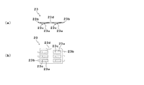
20はフレーム3内のカード挿入路5よりも上方に設けられたIC接点ユニットである。このIC接点ユニット20は、スライダ21、板ばね22、コネクタ23、およびコイルばね24から構成されている。各部の詳細を図1と図2に加え、図3〜図6を参照して説明する。なお、図3はスライダ21を示す図、図4は板ばね22を示す図、図5はコネクタ23を示す図、図6はIC接点ユニット20の組立図である(コイルばね24は図示省略)。また、各図において(a)はそれぞれの側面図、(b)はそれぞれの底面図((a)において下方から見た図)である。
An
スライダ21は、図3に示すように略凹形をした薄板から形成されている。このスライダ21は、上フレーム3aに支持されることにより、図1および図2に示すようにカード挿入路5と対面しかつカード挿入路5と平行にF、B方向へ移動可能に設けられている。スライダ21のF方向側には、フォトマイクロセンサ8のアクチュエータ8aと接触する接触片21aがF方向に向って突出するように形成されている。フォトマイクロセンサ8は、ICカード2がカード挿入路5の奥にある所定の位置まで完全に挿入されたことを検出するためのものである。なお、ICカード2は、先端2bがストッパ9(図1に図示)に当接するまでカード挿入路5にF方向へ挿入できる。接触片21aの傍には、カード挿入路5に挿入されたICカード2の先端2bと接触する爪21bが下方に向って突出するように形成されている。コイルばね24はそれぞれ、一端をスライダ21に引っ掛けられ、他端を上フレーム3aの壁3fに引っ掛けられている。このコイルばね24は、スライダ21をICカード2の反挿入方向Bに付勢している。
As shown in FIG. 3, the
板ばね22は、図4に示すように薄板を2段階曲げて形成されている。この板ばね22の下方に落ち込んだ一方の端部22aは、図6に示すようにスライダ21の横梁部21cの下面にスポット溶接または接着剤等により固定されている。また、板ばね22の上方に持ち上がった他方の端部22bの下面には、図6に示すようにコネクタ23を表面実装したFPC(Flexible Printed Circuit)25が両面テープまたは接着剤等により取り付けられている。板ばね22の中央に貫通された3つの孔22cには、図1および図2に示すようにカード挿入路5と対面するように上フレーム3aに設けられた突起3gが嵌まり込む。突起3gは、図1に示すようにICカード2の挿入方向Fに2つ、幅方向R、Lにコネクタ23を挟むように2つの合計4つが設けられている。突起3gのB方向側の側面と、当該側面に対向する板ばね22の側面とは、図2に示すようにICカード2の挿入方向Fに対してカード挿入路5に近づく方向(下方向)Dに所定角度で傾斜している。
The
コネクタ23は、図5に示すようにインサート成形により形成されていて、合成樹脂からなる基部23dと、導電性を有する複数の接触子23aとからなる。接触子23aのリード部23bは、図6(a)に示すようにFPC25にはんだ付けにより固定されていて、接点部23cは、図6(a)に示すようにスライダ21よりも下方へ突出している。フレーム3内において接触子23aは、図2に示すように板ばね22によってカード挿入路5から離れる方向(上方向)Uに付勢されてカード挿入路5より退避させられている。カード挿入路5にICカード2が挿入されると、接触子23aは、後述するように弾性変形して所定の圧力でICカード2のIC接点2aに接触する。FPC25は、フレーム3内に設けられている図示しない基板に接続されている。その基板には、ICカード2に対して情報の読み取りまたは書き込みの処理を行ったり、パーソナルコンピュータ等の上位装置と通信を行ったりするため等の制御回路が実装されている。
The
図7A〜図8Bは、上記ICカードリーダ1の動作を説明する図である。図7Aおよび図7BはICカードリーダ1の全体の平面図、図8Aおよび図8BはICカードリーダ1の要部を拡大した側方断面図である。図1に示した状態から、ICカード2がカード挿入路5にF方向へ挿入されて行くと、図7A(a)および図8A(a)に示すようにICカード2の先端2bがスライダ21の爪21bとプレート11の爪11aに接触する。これにより、スライダ21とプレート11が、ICカード2に押されてそれぞれ挿入方向Fへ移動して行く。
7A to 8B are diagrams for explaining the operation of the
スライダ21が挿入方向Fへ移動して行くことにより、図8A(b)に示すようにスライダ21に固定された板ばね22が突起3gに接触して、突起3gに沿ってカード挿入路5に近づく方向Dにたわんで行く。これにより、板ばね22に取り付けられたコネクタ23の接触子23aが下降して、カード挿入路5に進入して行き、ICカード2のIC接点2aに徐々に接触する。なお、ICカード2は下フレーム3bによって下面を支持されている。またこのとき、プレート11が挿入方向Fへ移動して行くことにより、図7A(b)に示すようにプレート11の爪11bとレバー12の端部12cとの接触位置がF方向にずれて行く。
As the
ICカード2がF方向へ挿入されて、スライダ21がF方向へ移動して行くことにより、図7B(c)に示すようにスライダ21の接触片21aがフォトマイクロセンサ8のアクチュエータ8aに接触すると、フォトマイクロセンサ8は、OFF状態からON状態に切り替わって、ICカード2がカード挿入路5の所定の位置まで完全に挿入されたことを検出する。このとき、ICカード2の先端2bがストッパ9に接触して、ICカード2のF方向への挿入が停止される。
When the
ICカード2が完全に挿入されると、図8B(c)に示すように板ばね22が突起3gの先端面(カード挿入路5側の面)に乗り上がって、ICカード2に最も近づいた状態となる。これにより、接触子23aが板ばね22に押されて弾性変形し、ICカード2のIC接点2aに所定の圧力で接触する。またこのとき、図7B(c)に示すようにレバー12の端部12cがプレート11の爪11bから外れて、レバー12がコイルばね15の弾性力によって反時計回りに回転する。これにより、レバー12の爪12aがICカード2の後端2cに接触して、ICカード2のカード挿入路5からの突出および抜き取りが阻止される。また、レバー12の爪12bがイジェクタピン13のフック部13cから外れて、イジェクタピン13の先端部13aがコイルばね16の弾性力によってフレーム3から外部に大きく突出する。
When the
上記のような状態になると、ICカードリーダ1は、接触子23aとICカード2のIC接点2aとを介してICカード2に通電し、ICカード2に対して情報の読み取りまたは書き込みの処理を行う。しばらくして、ICカードリーダ1がICカード2に対する情報の処理を終了した後、図7B(d)に示すようにイジェクタピン13の先端部13aが指でF方向に押されると、イジェクタピン13がF方向へ移動しながらフック部13cでレバー12の爪12bを引っ掛ける。これにより、レバー12の爪12bがフック部13cにR方向に押されて、レバー12が時計回りに回転する。レバー12が時計回りに回転すると、レバー12の爪12aがICカード2の後端2cから外れ、レバー12の端部12cがプレート11の爪11bのR方向側へ移動し、プレート11がコイルばね14の弾性力によってB方向に移動する。またこのとき、スライダ21がコイルばね24の弾性力によってB方向に移動し、この移動に伴って板ばね22が、図8B(d)に矢印で示すように突起3gに沿って移動して行って、カード挿入路5に近づく方向Dにたわまなくなる。これにより、接触子23aが、図8A(a)に示したように板ばね22によってカード挿入路5から離れる方向Uに付勢されて、カード挿入路5より退避させられた状態に戻る。上記のようにプレート11とスライダ21とがコイルばね14、24の弾性力によってB方向に移動すると、ICカード2がプレート11の爪11aとスライダ21の爪21bとに押されてカード挿入路5からB方向に突出し、ICカード2をカード挿入路5から抜き取り可能となる。
In such a state, the
以上のような構造にすることで、カード挿入路5へのICカード2の未挿入時には、板ばね22が接触子23aをカード挿入路5から離れる方向Uに付勢して退避させ、カード挿入路5へのICカード2の挿入時には、板ばね22がカード挿入路5に近づく方向Dにたわんで、接触子23aをICカード2のIC接点2aに接触させる。このため、接触子23aの変形や損傷を生じ難くなり、ICカードリーダ1の長寿命化を図ることが可能となる。また、接触子23aをスライダ21とともに移動する板ばね22に取り付け、当該板ばね22を突起3gに接触させてたわませることで、接触子23aがカード挿入路5より退避した位置からICカード2のIC接点2aに接触可能な位置まで移動する。このため、カード挿入路5の上方には接触子23aをカード挿入路5より退避させることが可能な比較的小さなスペース、即ち板ばね22の厚みと、FPC25の厚みと、接触子23aの高さ(リード部23bから接点部23cまでの高さ)と、接触子23aとカード挿入路5との若干のクリアランス等を加算したスペースだけを確保すればよくなり、ICカードリーダ1の薄型化を図ることが可能となる。
With the structure as described above, when the
また、上フレーム3aに突起3gをICカード2の挿入方向Fに2つ設け、板ばね22を各突起3gに接触させてカード挿入路5に近づく方向Dへたわませるようにしたことで、図8A(b)、図8B(c)に示すように板ばね22をカード挿入路5に対して略平行にたわませて、接触子23aをICカード2のIC接点2aに突き当てることなく安定に接触させることができ、接触子23aの変形や損傷を一層生じ難くすることが可能となる。
In addition, two
さらに、突起3gと板ばね22の互いに接触する部分を、ICカード2の挿入方向Fに対してカード挿入路5に近づく方向Dに傾斜させたことで、板ばね22を突起3gに突き当てることなく、突起3gに沿ってスムーズにカード挿入路5に近づく方向Dにたわませて、接触子23aをICカード2のIC接点2aに徐々に接触させることができ、接触子23aの変形や損傷を一層生じ難くすることが可能となる。
Furthermore, the part which the
本発明は、以上述べた実施形態以外にも種々の形態を採用することができる。例えば、以上の実施形態では、上フレーム3aに突起3gをICカード2の挿入方向Fに2つ、幅方向R、Lに2つの合計4つ設けた例を挙げたが、本発明はこれのみに限定するものではない。これ以外に、例えば突起3gを、ICカード2の挿入方向Fに3つ以上設けるようにしてもよいし、幅方向R、Lに3つ以上設けるようにしてもよい。
The present invention can adopt various forms other than the embodiment described above. For example, in the above embodiment, an example in which two
また、以上の実施形態では、突起3gと板ばね22の互いに接触する部分を、ICカード2の挿入方向Fに対して下方向Dに所定角度で直線的に傾斜させた例を挙げたが、本発明はこれのみに限定するものではない。これ以外に、例えば突起3gと板ばね22の互いに接触する部分を、挿入方向Fに対して下方向Dに曲線的に傾斜させるようにしてもよい。また、突起3gと板ばね22のいずれか一方を直線的に傾斜させ、他方を曲線的に傾斜させるようにしたり、突起3gと板ばね22のいずれか一方のみを直線的または曲線的に傾斜させるようにしたりしてもよい。
Further, in the above embodiment, the example in which the portions of the
さらに、以上の実施形態では、接触式のICカード2専用のICカードリーダ1に本発明を適用したが、本発明はこれ以外にも、例えばIC接点と磁気ストライプの両方が設けられた磁気ICカードに対して情報の処理を行えるように、IC接点ユニットと磁気ヘッドとを内部に備えたICカードリーダに適用することが可能である。また、例えばカード挿入路に挿入されたICカードを自動的に内部へ搬送するローラ等の搬送手段を備えたICカードリーダに適用することが可能である。
Further, in the above embodiment, the present invention is applied to the
1 ICカードリーダ
2 ICカード
2a IC接点
2b ICカードの先端
3a 上フレーム
3b 下フレーム
3g 突起
5 カード挿入路
21 スライダ
21b 爪
22 板ばね
23a 接触子
24 コイルばね
B ICカードの反挿入方向
F ICカードの挿入方向
DESCRIPTION OF
Claims (1)
ICカードのIC接点に接触する接触子と、
前記カード挿入路と対面しつつ平行に移動可能に設けられたスライダと、
前記カード挿入路に挿入されたICカードの先端と接触するように前記スライダに設けられた爪と、
前記スライダをICカードの反挿入方向に付勢するばねと、
一方の端部が前記スライダに固定され、他方の端部に前記カード挿入路と対面するように前記接触子が取り付けられ、当該接触子を前記カード挿入路から離れる方向に付勢して前記カード挿入路より退避させる板ばねと、
前記カード挿入路と対面するように前記フレームに設けられた突起と、を備え、
前記突起は、ICカードの挿入方向に少なくとも2つ設けられており、
ICカードが前記カード挿入路に挿入されることにより、ICカードの先端が前記爪と接触して、前記スライダがICカードの挿入方向へ移動するときに、前記板ばねが前記突起に接触して前記カード挿入路に近づく方向に、当該カード挿入路に対して略平行にたわみ、前記接触子を前記カード挿入路に進入させてICカードのIC接点に接触させ、
前記突起と前記板ばねの互いに接触する部分を、ICカードの挿入方向に対して前記カード挿入路に近づく方向に傾斜させたことを特徴とするICカードリーダ。 A frame in which a card insertion path into which an IC card is inserted is formed;
A contact that contacts the IC contact of the IC card;
A slider provided so as to be movable in parallel while facing the card insertion path;
A claw provided on the slider so as to come into contact with the tip of the IC card inserted into the card insertion path;
A spring for urging the slider in the anti-insertion direction of the IC card;
One end is fixed to the slider, and the contact is attached to the other end so as to face the card insertion path, and the card is urged in a direction away from the card insertion path. A leaf spring retracted from the insertion path;
A projection provided on the frame so as to face the card insertion path,
At least two of the protrusions are provided in the insertion direction of the IC card,
When the IC card is inserted into the card insertion path, the tip of the IC card comes into contact with the claw, and when the slider moves in the IC card insertion direction, the leaf spring comes into contact with the protrusion. In the direction approaching the card insertion path, bends substantially parallel to the card insertion path, the contactor enters the card insertion path to contact the IC contact of the IC card ,
An IC card reader , wherein a portion of the protrusion and the leaf spring contacting each other is inclined in a direction approaching the card insertion path with respect to an IC card insertion direction .
Priority Applications (6)
| Application Number | Priority Date | Filing Date | Title |
|---|---|---|---|
| JP2004075552A JP4363636B2 (en) | 2004-03-17 | 2004-03-17 | IC card reader |
| EP05005487A EP1577826B1 (en) | 2004-03-17 | 2005-03-14 | IC card reader |
| DE602005021269T DE602005021269D1 (en) | 2004-03-17 | 2005-03-14 | Smart card reader |
| AT05005487T ATE468567T1 (en) | 2004-03-17 | 2005-03-14 | CHIP CARD READER |
| CNB2005100555487A CN100365649C (en) | 2004-03-17 | 2005-03-16 | IC card reader |
| US11/080,510 US7370804B2 (en) | 2004-03-17 | 2005-03-16 | IC card reader |
Applications Claiming Priority (1)
| Application Number | Priority Date | Filing Date | Title |
|---|---|---|---|
| JP2004075552A JP4363636B2 (en) | 2004-03-17 | 2004-03-17 | IC card reader |
Publications (2)
| Publication Number | Publication Date |
|---|---|
| JP2005266993A JP2005266993A (en) | 2005-09-29 |
| JP4363636B2 true JP4363636B2 (en) | 2009-11-11 |
Family
ID=34836527
Family Applications (1)
| Application Number | Title | Priority Date | Filing Date |
|---|---|---|---|
| JP2004075552A Expired - Fee Related JP4363636B2 (en) | 2004-03-17 | 2004-03-17 | IC card reader |
Country Status (6)
| Country | Link |
|---|---|
| US (1) | US7370804B2 (en) |
| EP (1) | EP1577826B1 (en) |
| JP (1) | JP4363636B2 (en) |
| CN (1) | CN100365649C (en) |
| AT (1) | ATE468567T1 (en) |
| DE (1) | DE602005021269D1 (en) |
Families Citing this family (20)
| Publication number | Priority date | Publication date | Assignee | Title |
|---|---|---|---|---|
| TWI226586B (en) * | 2002-09-20 | 2005-01-11 | Fci Asia Technology Pte Ltd | Anti-misinsertion mechanism |
| JP2008152492A (en) * | 2006-12-15 | 2008-07-03 | Hitachi Omron Terminal Solutions Corp | Card reader |
| US20080182622A1 (en) * | 2007-01-25 | 2008-07-31 | Sierra Wireless, Inc. | Method and Apparatus for Implementing a SIM Card Onboard a PC Card |
| JP5030678B2 (en) * | 2007-06-15 | 2012-09-19 | 日立オムロンターミナルソリューションズ株式会社 | Recording medium processing apparatus |
| WO2010137161A1 (en) * | 2009-05-29 | 2010-12-02 | 富士通フロンテック株式会社 | Magnetic card reader |
| DE102013001470A1 (en) * | 2013-01-29 | 2014-07-31 | Amphenol-Tuchel Electronics Gmbh | Rocking actuator for a push-push card reader |
| US11080674B1 (en) | 2014-09-19 | 2021-08-03 | Square, Inc. | Point of sale system |
| US9286494B1 (en) | 2014-11-20 | 2016-03-15 | Square, Inc. | Card reader having discriminator contact |
| US10783508B1 (en) | 2014-12-16 | 2020-09-22 | Square, Inc. | Processing multiple point-of-sale transactions |
| JP2016122376A (en) * | 2014-12-25 | 2016-07-07 | 日本電産サンキョー株式会社 | Card reader |
| US10318952B1 (en) | 2015-05-23 | 2019-06-11 | Square, Inc. | NFC base station and passive transmitter device |
| US11080675B1 (en) | 2015-09-08 | 2021-08-03 | Square, Inc. | Point-of-sale system having a secure touch mode |
| US9721123B1 (en) | 2015-12-11 | 2017-08-01 | Square, Inc. | Microcontroller intercept of EMV card contact switch |
| US10607200B2 (en) | 2015-12-28 | 2020-03-31 | Square, Inc. | Point of sale system having a customer terminal and a merchant terminal |
| US10504092B2 (en) | 2016-06-21 | 2019-12-10 | Square, Inc. | Transaction interface control |
| US10402816B2 (en) | 2016-12-31 | 2019-09-03 | Square, Inc. | Partial data object acquisition and processing |
| US9858448B1 (en) | 2017-01-31 | 2018-01-02 | Square, Inc. | Communication protocol speedup and step-down |
| US10438189B2 (en) | 2017-02-22 | 2019-10-08 | Square, Inc. | Server-enabled chip card interface tamper detection |
| US10621590B2 (en) | 2017-02-22 | 2020-04-14 | Square, Inc. | Line-based chip card tamper detection |
| US10181061B2 (en) * | 2017-05-11 | 2019-01-15 | Verifone, Inc. | Systems, methods and devices for concealed EMV chip card readers |
Family Cites Families (16)
| Publication number | Priority date | Publication date | Assignee | Title |
|---|---|---|---|---|
| FR2594988B1 (en) * | 1986-02-21 | 1989-11-24 | Radiotechnique Ind & Comm | APPARATUS FOR ESTABLISHING DATA TRANSFERS WITH A PORTABLE ELECTRONIC CARD |
| JP2593143B2 (en) | 1986-05-20 | 1997-03-26 | 日立マクセル株式会社 | IC card reader / writer |
| US4904852A (en) * | 1986-12-12 | 1990-02-27 | Omron Tateisi Electronics Co. | IC card reader |
| US4839509A (en) * | 1987-06-19 | 1989-06-13 | Diesel Kiki Co., Ltd. | Connector device for connecting IC card to reading and/or writing apparatus |
| AT394462B (en) * | 1990-06-01 | 1992-04-10 | Philips Nv | SCANNER DEVICE FOR A CHIP CARD |
| DE4316303B4 (en) * | 1993-05-14 | 2010-09-09 | Amphenol-Tuchel Electronics Gmbh | Chip card contacting device with positively opened contacts |
| JP2660655B2 (en) * | 1993-12-16 | 1997-10-08 | アンリツ株式会社 | IC card processing device |
| JP3131553B2 (en) * | 1995-05-15 | 2001-02-05 | 株式会社三協精機製作所 | IC card reader |
| JP3559368B2 (en) | 1995-11-17 | 2004-09-02 | 株式会社東芝 | IC card processing device |
| JPH1063792A (en) | 1996-08-27 | 1998-03-06 | Matsushita Electric Ind Co Ltd | Ic card readering and writing apparatus |
| JP3372814B2 (en) * | 1997-03-07 | 2003-02-04 | 株式会社三協精機製作所 | IC card reader |
| CN2368085Y (en) * | 1999-01-08 | 2000-03-08 | 李素琴 | IC-card reader |
| KR100341226B1 (en) * | 1999-11-23 | 2002-06-20 | 정진택 | Compact type connecter soldering printed circuit board |
| CN2423619Y (en) * | 2000-01-25 | 2001-03-14 | 娄云才 | IC and read/write device with current conducting device |
| MXPA02003930A (en) * | 2000-08-31 | 2002-10-23 | Anritsu Corp | Ic card handling device. |
| JP3828003B2 (en) * | 2001-12-04 | 2006-09-27 | 日本電産サンキョー株式会社 | IC card reader |
-
2004
- 2004-03-17 JP JP2004075552A patent/JP4363636B2/en not_active Expired - Fee Related
-
2005
- 2005-03-14 DE DE602005021269T patent/DE602005021269D1/en active Active
- 2005-03-14 EP EP05005487A patent/EP1577826B1/en not_active Not-in-force
- 2005-03-14 AT AT05005487T patent/ATE468567T1/en not_active IP Right Cessation
- 2005-03-16 US US11/080,510 patent/US7370804B2/en not_active Expired - Fee Related
- 2005-03-16 CN CNB2005100555487A patent/CN100365649C/en not_active Expired - Fee Related
Also Published As
| Publication number | Publication date |
|---|---|
| CN100365649C (en) | 2008-01-30 |
| US20050211779A1 (en) | 2005-09-29 |
| DE602005021269D1 (en) | 2010-07-01 |
| EP1577826B1 (en) | 2010-05-19 |
| CN1670760A (en) | 2005-09-21 |
| EP1577826A2 (en) | 2005-09-21 |
| JP2005266993A (en) | 2005-09-29 |
| US7370804B2 (en) | 2008-05-13 |
| EP1577826A3 (en) | 2008-05-14 |
| ATE468567T1 (en) | 2010-06-15 |
Similar Documents
| Publication | Publication Date | Title |
|---|---|---|
| JP4363636B2 (en) | IC card reader | |
| US7381094B2 (en) | Card connector | |
| JP4351826B2 (en) | Card connector device | |
| JP3823038B2 (en) | Card connector device | |
| KR101291884B1 (en) | Magnetic card reader | |
| JP3859625B2 (en) | Memory card connector | |
| JP3961224B2 (en) | Card connector device | |
| KR101035466B1 (en) | Connector for memory card | |
| US6179638B1 (en) | Connector for use in a card reader | |
| US20100038429A1 (en) | Medium processing device and method of controlling the same | |
| US6652300B2 (en) | Card connector device having slide member for discharging card | |
| US20100327851A1 (en) | Contact mechanism, card detecting apparatus, and card detecting method | |
| JP2002313485A (en) | Connector for card | |
| JP3827578B2 (en) | Card connector device | |
| JP2005322100A (en) | Ic card reader | |
| JP5067668B2 (en) | IC card connector | |
| JP3492542B2 (en) | Proximity switch for IC card | |
| JP2003142207A (en) | Card connector | |
| JP2002252060A (en) | Connector for card | |
| JP2003142204A (en) | Card connector | |
| JPS60167066A (en) | Reader/writer of ic card | |
| JP2003142201A (en) | Card connector | |
| JP2015005333A (en) | Card connector with ejection mechanism | |
| JP2002252046A (en) | Connector for card | |
| JP2010009865A (en) | Memory card socket |
Legal Events
| Date | Code | Title | Description |
|---|---|---|---|
| A621 | Written request for application examination |
Free format text: JAPANESE INTERMEDIATE CODE: A621 Effective date: 20060706 |
|
| A977 | Report on retrieval |
Free format text: JAPANESE INTERMEDIATE CODE: A971007 Effective date: 20090415 |
|
| A131 | Notification of reasons for refusal |
Free format text: JAPANESE INTERMEDIATE CODE: A131 Effective date: 20090428 |
|
| A521 | Request for written amendment filed |
Free format text: JAPANESE INTERMEDIATE CODE: A523 Effective date: 20090615 |
|
| TRDD | Decision of grant or rejection written | ||
| A01 | Written decision to grant a patent or to grant a registration (utility model) |
Free format text: JAPANESE INTERMEDIATE CODE: A01 Effective date: 20090817 |
|
| A01 | Written decision to grant a patent or to grant a registration (utility model) |
Free format text: JAPANESE INTERMEDIATE CODE: A01 |
|
| A61 | First payment of annual fees (during grant procedure) |
Free format text: JAPANESE INTERMEDIATE CODE: A61 Effective date: 20090817 |
|
| FPAY | Renewal fee payment (event date is renewal date of database) |
Free format text: PAYMENT UNTIL: 20120828 Year of fee payment: 3 |
|
| R150 | Certificate of patent or registration of utility model |
Free format text: JAPANESE INTERMEDIATE CODE: R150 |
|
| FPAY | Renewal fee payment (event date is renewal date of database) |
Free format text: PAYMENT UNTIL: 20130828 Year of fee payment: 4 |
|
| LAPS | Cancellation because of no payment of annual fees |