JP4330396B2 - 半導体記憶装置 - Google Patents
半導体記憶装置 Download PDFInfo
- Publication number
- JP4330396B2 JP4330396B2 JP2003279239A JP2003279239A JP4330396B2 JP 4330396 B2 JP4330396 B2 JP 4330396B2 JP 2003279239 A JP2003279239 A JP 2003279239A JP 2003279239 A JP2003279239 A JP 2003279239A JP 4330396 B2 JP4330396 B2 JP 4330396B2
- Authority
- JP
- Japan
- Prior art keywords
- data
- signal
- memory cell
- write
- circuit
- Prior art date
- Legal status (The legal status is an assumption and is not a legal conclusion. Google has not performed a legal analysis and makes no representation as to the accuracy of the status listed.)
- Expired - Fee Related
Links
Images


Classifications
-
- G—PHYSICS
- G11—INFORMATION STORAGE
- G11C—STATIC STORES
- G11C11/00—Digital stores characterised by the use of particular electric or magnetic storage elements; Storage elements therefor
- G11C11/21—Digital stores characterised by the use of particular electric or magnetic storage elements; Storage elements therefor using electric elements
- G11C11/34—Digital stores characterised by the use of particular electric or magnetic storage elements; Storage elements therefor using electric elements using semiconductor devices
- G11C11/40—Digital stores characterised by the use of particular electric or magnetic storage elements; Storage elements therefor using electric elements using semiconductor devices using transistors
- G11C11/41—Digital stores characterised by the use of particular electric or magnetic storage elements; Storage elements therefor using electric elements using semiconductor devices using transistors forming static cells with positive feedback, i.e. cells not needing refreshing or charge regeneration, e.g. bistable multivibrator or Schmitt trigger
- G11C11/413—Auxiliary circuits, e.g. for addressing, decoding, driving, writing, sensing, timing or power reduction
- G11C11/417—Auxiliary circuits, e.g. for addressing, decoding, driving, writing, sensing, timing or power reduction for memory cells of the field-effect type
- G11C11/419—Read-write [R-W] circuits
-
- G—PHYSICS
- G11—INFORMATION STORAGE
- G11C—STATIC STORES
- G11C11/00—Digital stores characterised by the use of particular electric or magnetic storage elements; Storage elements therefor
- G11C11/21—Digital stores characterised by the use of particular electric or magnetic storage elements; Storage elements therefor using electric elements
- G11C11/34—Digital stores characterised by the use of particular electric or magnetic storage elements; Storage elements therefor using electric elements using semiconductor devices
- G11C11/40—Digital stores characterised by the use of particular electric or magnetic storage elements; Storage elements therefor using electric elements using semiconductor devices using transistors
- G11C11/41—Digital stores characterised by the use of particular electric or magnetic storage elements; Storage elements therefor using electric elements using semiconductor devices using transistors forming static cells with positive feedback, i.e. cells not needing refreshing or charge regeneration, e.g. bistable multivibrator or Schmitt trigger
- G11C11/413—Auxiliary circuits, e.g. for addressing, decoding, driving, writing, sensing, timing or power reduction
- G11C11/417—Auxiliary circuits, e.g. for addressing, decoding, driving, writing, sensing, timing or power reduction for memory cells of the field-effect type
-
- G—PHYSICS
- G11—INFORMATION STORAGE
- G11C—STATIC STORES
- G11C5/00—Details of stores covered by group G11C11/00
- G11C5/06—Arrangements for interconnecting storage elements electrically, e.g. by wiring
- G11C5/063—Voltage and signal distribution in integrated semi-conductor memory access lines, e.g. word-line, bit-line, cross-over resistance, propagation delay
-
- G—PHYSICS
- G11—INFORMATION STORAGE
- G11C—STATIC STORES
- G11C7/00—Arrangements for writing information into, or reading information out from, a digital store
- G11C7/10—Input/output [I/O] data interface arrangements, e.g. I/O data control circuits, I/O data buffers
- G11C7/1051—Data output circuits, e.g. read-out amplifiers, data output buffers, data output registers, data output level conversion circuits
-
- G—PHYSICS
- G11—INFORMATION STORAGE
- G11C—STATIC STORES
- G11C7/00—Arrangements for writing information into, or reading information out from, a digital store
- G11C7/10—Input/output [I/O] data interface arrangements, e.g. I/O data control circuits, I/O data buffers
- G11C7/1075—Input/output [I/O] data interface arrangements, e.g. I/O data control circuits, I/O data buffers for multiport memories each having random access ports and serial ports, e.g. video RAM
-
- G—PHYSICS
- G11—INFORMATION STORAGE
- G11C—STATIC STORES
- G11C7/00—Arrangements for writing information into, or reading information out from, a digital store
- G11C7/10—Input/output [I/O] data interface arrangements, e.g. I/O data control circuits, I/O data buffers
- G11C7/1078—Data input circuits, e.g. write amplifiers, data input buffers, data input registers, data input level conversion circuits
Description
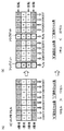
図1は、この発明の実施の形態1による半導体記憶装置1Aの概略的な構成を示したブロック図である。
図13は、この発明の実施の形態2による半導体記憶装置1Bの概略的な構成を示したブロック図である。
Claims (7)
- 行列状に配置される複数のメモリセルを含むメモリセルアレイと、
データ信号を入力し、前記データ信号においてローレベルの論理値の数がハイレベルの論理値の数より多い場合に前記データ信号を反転し、反転または非反転の前記データ信号および前記データ信号が反転および非反転のいずれであるかを示す前記データ信号のフラグ信号を前記メモリセルに書き込むデータ入力回路と、
反転または非反転の前記データ信号および該データ信号の前記フラグ信号を前記メモリセルから読み出し、前記フラグ信号が反転を示す場合、反転または非反転の前記データ信号を再度反転するデータ出力回路とを備え、
前記複数のメモリセルの各々は、
第1の記憶ノードと第2の記憶ノードとの間に互いに環状に接続された第1のインバータと第2のインバータとを有し、データを記憶保持するデータ記憶部と、
前記データ記憶部からデータを読み出す読出ポート部と、
前記データ記憶部にデータを書き込む書込ポート部とを含み、
前記読出ポート部は、
行方向に配置される読出ワード線と、
列方向に配置される読出ビット線と、
第1の電源線と前記読出ビット線との間に直列に接続され、ゲートが前記第1の記憶ノードに接続される第1のトランジスタと、
前記第1のトランジスタに接続され、ゲートが前記読出ワード線に接続される第2のトランジスタとを有し、
前記書込ポート部は、
行方向に配置される第1の書込ビット線と、
列方向に配置される第2の書込ビット線と、
列方向に配置される書込ワード線と、
前記第1の記憶ノードと前記第1の書込ビット線との間に接続され、ゲートが前記書込ワード線に接続される第3のトランジスタと、
前記第2の記憶ノードと前記第2の書込ビット線との間に接続され、ゲートが前記書込ワード線に接続される第4のトランジスタとを有し、
前記データ記憶部は、
前記論理値がローレベルの場合に、前記第1の記憶ノードが第1の電位レベルで、前記第2の記憶ノードが前記第1の電位レベルよりも低い第2の電位レベルで、データをそれぞれ記憶保持し、
前記論理値がハイレベルの場合は、前記第1の記憶ノードが前記第2の電位レベルで、前記第2の記憶ノードが前記第1の電位レベルで、データをそれぞれ記憶保持し、
前記読出ビット線は、読出し動作時に前記第1の電位レベルにプリチャージされ、前記第1の記憶ノードの電位レベルに応じてその電位レベルが維持または低下される、半導体記憶装置。 - 前記データ入力回路は、
前記データ信号におけるローレベルの論理値の数とハイレベルの論理値の数とを比較し、該比較結果に応じて前記フラグ信号を反転または非反転とする多数決論理判定回路と、
前記フラグ信号に応じて、前記データ信号の反転信号および非反転信号のいずれか一方を選択するセレクタ回路と、
書込制御信号に応じて、前記セレクタ回路からの出力信号を前記メモリセルに書き込む書込みドライバ回路とを含む、請求項1に記載の半導体記憶装置。 - 前記データ出力回路は、
前記メモリセルから読み出されるデータがローレベルの論理値であるかハイレベルの論理値であるかを逐次判定するセンスアンプ回路と、
前記フラグ信号に応じて、前記センスアンプ回路からの出力信号の反転信号および非反転信号のいずれか一方を選択するセレクタ回路と、
データ出力制御信号に応じて、前記セレクタ回路からの出力信号をデータ出力信号として出力するバッファ回路とを含む、請求項1に記載の半導体記憶装置。 - 前記データ入力回路は、前記データ信号のビット分割を行い、該ビット分割に応じて前記フラグ信号のフラグビットを複数設ける、請求項1に記載の半導体記憶装置。
- 前記データ入力回路は、
クロック信号に同期して、前記データ信号をラッチするとともに、多数決線対の電位レベルを制御する複数のフリップフロップ回路と、
前記多数決線対の電位レベルに応じて、多数決論理判定信号を出力するセンスアンプ回路と、
前記多数決論理判定信号に応じて、前記複数のフリップフロップ回路からの出力信号の反転信号および非反転信号のいずれか一方を選択する複数のセレクタ回路と、
書込制御信号に応じて、前記複数のセレクタ回路からの出力信号を前記メモリセルに書き込む複数の書込みドライバ回路とを含む、請求項1に記載の半導体記憶装置。 - 行列状に配置され、それぞれが、第1の記憶ノードと第2の記憶ノードとの間に互いに環状に接続された第1のインバータと第2のインバータとを有し、データを記憶保持するデータ記憶部と、前記データ記憶部からデータを読み出す読出ポート部と、前記データ記憶部にデータを書き込む書込ポート部とを含む、複数のデータを記憶するデータビット用メモリセルと、行ごとに設けられ前記データビット用メモリセルの記憶データの反転情報を記憶するフラグビット用メモリセルとを有するメモリセルアレイと、
前記メモリセルアレイの行方向に行ごとに前記データビット用メモリセルの読出ポートおよび前記フラグビット用メモリセルに接続される複数の読出ワード線と、
前記メモリセルアレイの列方向に列ごとに前記メモリセルの読出ポートに接続される複数の読出ビット線と、
前記データビット用メモリセルに書き込まれるデータ入力信号において、ローレベルの論理値がハイレベルの論理値に比較し読み出し時にメモリセルに流れる電流が多いものであり、一方の論理値の数が他方の論理値の数より多い行がある場合、その行のフラグビット用メモリセルにその行の前記データビット用メモリセルのデータが反転データである旨を示すデータを書き込み、その行の前記データ入力信号を反転したデータをその行のデータビット用メモリセルに書き込むデータ入力回路と、
前記フラグビット用メモリセルのデータが反転である旨を示すデータである場合、対応の行の前記データビット用メモリセルのデータを反転して読み出すデータ出力回路とを備え、
前記書込ポート部は、
行方向に配置される第1の書込ビット線と、
列方向に配置される第2の書込ビット線と、
列方向に配置される書込ワード線とを有し、
前記データ記憶部は、
前記論理値がローレベルの場合に、前記第1の記憶ノードが第1の電位レベルで、前記第2の記憶ノードが前記第1の電位レベルよりも低い第2の電位レベルで、データをそれぞれ記憶保持し、
前記論理値がハイレベルの場合は、前記第1の記憶ノードが前記第2の電位レベルで、前記第2の記憶ノードが前記第1の電位レベルで、データをそれぞれ記憶保持し、
前記読出ビット線は、読出し動作時に前記第1の電位レベルにプリチャージされ、前記第1の記憶ノードの電位レベルに応じてその電位レベルが維持または低下される、半導体記憶装置。 - 前記データ入力回路は、
前記データ入力信号におけるローレベルの論理値の数とハイレベルの論理値の数とを比較し、該比較結果に応じて、対応行の前記フラグビット用メモリセルの信号を反転または非反転を示すデータとする多数決論理判定回路と、
前記フラグビット用メモリセルの信号に応じて、前記データ入力信号の反転信号および非反転信号のいずれか一方を選択するセレクタ回路と、
書込制御信号に応じて、前記セレクタ回路からの出力信号を前記メモリセルに書き込む書込みドライバ回路とを含む、請求項6に記載の半導体記憶装置。
Priority Applications (4)
| Application Number | Priority Date | Filing Date | Title |
|---|---|---|---|
| JP2003279239A JP4330396B2 (ja) | 2003-07-24 | 2003-07-24 | 半導体記憶装置 |
| KR1020040056297A KR100633815B1 (ko) | 2003-07-24 | 2004-07-20 | 판독 시 및 대기 시에 있어서의 소비 전력을 저감하는것이 가능한 반도체 기억 장치 |
| US10/895,092 US6999371B2 (en) | 2003-07-24 | 2004-07-21 | Semiconductor memory device capable of reducing power consumption during reading and standby |
| US11/304,817 US7170812B2 (en) | 2003-07-24 | 2005-12-16 | Semiconductor memory device capable of reducing power consumption during reading and standby |
Applications Claiming Priority (1)
| Application Number | Priority Date | Filing Date | Title |
|---|---|---|---|
| JP2003279239A JP4330396B2 (ja) | 2003-07-24 | 2003-07-24 | 半導体記憶装置 |
Publications (3)
| Publication Number | Publication Date |
|---|---|
| JP2005044456A JP2005044456A (ja) | 2005-02-17 |
| JP2005044456A5 JP2005044456A5 (ja) | 2006-08-17 |
| JP4330396B2 true JP4330396B2 (ja) | 2009-09-16 |
Family
ID=34074745
Family Applications (1)
| Application Number | Title | Priority Date | Filing Date |
|---|---|---|---|
| JP2003279239A Expired - Fee Related JP4330396B2 (ja) | 2003-07-24 | 2003-07-24 | 半導体記憶装置 |
Country Status (3)
| Country | Link |
|---|---|
| US (2) | US6999371B2 (ja) |
| JP (1) | JP4330396B2 (ja) |
| KR (1) | KR100633815B1 (ja) |
Families Citing this family (60)
| Publication number | Priority date | Publication date | Assignee | Title |
|---|---|---|---|---|
| JP4330396B2 (ja) * | 2003-07-24 | 2009-09-16 | 株式会社ルネサステクノロジ | 半導体記憶装置 |
| JP4322645B2 (ja) * | 2003-11-28 | 2009-09-02 | 株式会社日立製作所 | 半導体集積回路装置 |
| WO2005122177A1 (ja) * | 2004-06-09 | 2005-12-22 | Matsushita Electric Industrial Co., Ltd. | 半導体集積回路 |
| KR100571647B1 (ko) * | 2005-03-31 | 2006-04-17 | 주식회사 하이닉스반도체 | 반도체 장치의 데이터 래치회로 |
| US7295487B2 (en) * | 2005-05-19 | 2007-11-13 | Freescale Semiconductor, Inc. | Storage circuit and method therefor |
| EP1750276B1 (en) * | 2005-07-29 | 2017-03-08 | Semiconductor Energy Laboratory Co., Ltd. | Semiconductor device |
| JP2007059044A (ja) * | 2005-07-29 | 2007-03-08 | Semiconductor Energy Lab Co Ltd | 半導体装置 |
| JP4954626B2 (ja) * | 2005-07-29 | 2012-06-20 | 株式会社半導体エネルギー研究所 | 半導体装置 |
| KR100621353B1 (ko) | 2005-11-08 | 2006-09-07 | 삼성전자주식회사 | 데이터 반전 확인 기능을 가지는 데이터 입출력 회로 및이를 포함하는 반도체 메모리 장치 |
| US7372763B2 (en) * | 2005-12-28 | 2008-05-13 | Intel Corporation | Memory with spatially encoded data storage |
| JP4928830B2 (ja) | 2006-05-18 | 2012-05-09 | 株式会社東芝 | Nand型フラッシュメモリ装置及びメモリデバイス |
| US7565586B2 (en) * | 2006-05-25 | 2009-07-21 | Honeywell International Inc. | Method and apparatus for latent fault memory scrub in memory intensive computer hardware |
| KR100735758B1 (ko) | 2006-06-29 | 2007-07-06 | 삼성전자주식회사 | 다수 판정 회로, 데이터 버스 반전 회로 및 반도체 장치. |
| US7688102B2 (en) | 2006-06-29 | 2010-03-30 | Samsung Electronics Co., Ltd. | Majority voter circuits and semiconductor devices including the same |
| KR100827663B1 (ko) | 2006-12-20 | 2008-05-07 | 삼성전자주식회사 | 다수 판정 회로 및 반도체 장치. |
| KR100780955B1 (ko) * | 2006-08-14 | 2007-12-03 | 삼성전자주식회사 | 데이터 반전 방식을 사용하는 메모리 시스템 |
| JP2008059717A (ja) * | 2006-09-01 | 2008-03-13 | Kobe Univ | 半導体装置 |
| US8411709B1 (en) | 2006-11-27 | 2013-04-02 | Marvell International Ltd. | Use of previously buffered state information to decode in an hybrid automatic repeat request (H-ARQ) transmission mode |
| US7468929B2 (en) * | 2006-12-12 | 2008-12-23 | International Business Machines Corporation | Apparatus for SRAM array power reduction through majority evaluation |
| US8763114B2 (en) * | 2007-01-24 | 2014-06-24 | Mcafee, Inc. | Detecting image spam |
| KR100819061B1 (ko) * | 2007-03-06 | 2008-04-03 | 한국전자통신연구원 | 쓰기 전력 계산 및 데이터 반전 기능을 통한 상 변화메모리에서의 데이터 쓰기 장치 및 방법 |
| US7577015B2 (en) * | 2007-03-30 | 2009-08-18 | Intel Corporation | Memory content inverting to minimize NTBI effects |
| US7990796B2 (en) * | 2007-04-05 | 2011-08-02 | Lsi Corporation | Energy efficient memory access technique for single ended bit cells |
| US7525864B2 (en) * | 2007-04-05 | 2009-04-28 | Lsi Corporation | Memory data inversion architecture for minimizing power consumption |
| US7606061B2 (en) * | 2007-08-07 | 2009-10-20 | Taiwan Semiconductor Manufacturing Co., Ltd. | SRAM device with a power saving module controlled by word line signals |
| US8897393B1 (en) | 2007-10-16 | 2014-11-25 | Marvell International Ltd. | Protected codebook selection at receiver for transmit beamforming |
| US8542725B1 (en) | 2007-11-14 | 2013-09-24 | Marvell International Ltd. | Decision feedback equalization for signals having unequally distributed patterns |
| US8565325B1 (en) | 2008-03-18 | 2013-10-22 | Marvell International Ltd. | Wireless device communication in the 60GHz band |
| US8064269B2 (en) | 2008-05-02 | 2011-11-22 | Micron Technology, Inc. | Apparatus and methods having majority bit detection |
| US8761261B1 (en) | 2008-07-29 | 2014-06-24 | Marvell International Ltd. | Encoding using motion vectors |
| US8498342B1 (en) | 2008-07-29 | 2013-07-30 | Marvell International Ltd. | Deblocking filtering |
| JP5289855B2 (ja) * | 2008-08-07 | 2013-09-11 | ルネサスエレクトロニクス株式会社 | 半導体集積回路 |
| US8345533B1 (en) | 2008-08-18 | 2013-01-01 | Marvell International Ltd. | Frame synchronization techniques |
| JP4937219B2 (ja) | 2008-09-17 | 2012-05-23 | 株式会社東芝 | 不揮発性半導体記憶装置 |
| US7978493B1 (en) * | 2008-09-18 | 2011-07-12 | Altera Corporation | Data encoding scheme to reduce sense current |
| US8681893B1 (en) * | 2008-10-08 | 2014-03-25 | Marvell International Ltd. | Generating pulses using a look-up table |
| US8081521B2 (en) * | 2009-02-13 | 2011-12-20 | Mosys, Inc. | Two bits per cell non-volatile memory architecture |
| US8520771B1 (en) | 2009-04-29 | 2013-08-27 | Marvell International Ltd. | WCDMA modulation |
| JP2010272190A (ja) * | 2009-05-25 | 2010-12-02 | Panasonic Corp | 半導体記憶装置 |
| JP2011008850A (ja) * | 2009-06-24 | 2011-01-13 | Sony Corp | メモリ及び情報処理方法 |
| EP2267724A1 (fr) * | 2009-06-26 | 2010-12-29 | STMicroelectronics Rousset SAS | Architecture de mémoire EEPROM optimisée pour les mémoires embarquées |
| US8218380B2 (en) * | 2009-10-30 | 2012-07-10 | Apple Inc. | Degradation equalization for a memory |
| US20110246857A1 (en) * | 2010-04-02 | 2011-10-06 | Samsung Electronics Co., Ltd. | Memory system and method |
| US8817771B1 (en) | 2010-07-16 | 2014-08-26 | Marvell International Ltd. | Method and apparatus for detecting a boundary of a data frame in a communication network |
| JP5751628B2 (ja) * | 2011-09-09 | 2015-07-22 | Necプラットフォームズ株式会社 | 記憶装置および記憶装置制御方法 |
| JP5186587B1 (ja) * | 2011-09-29 | 2013-04-17 | 株式会社アドバンテスト | 試験装置および試験方法 |
| CN104067247A (zh) * | 2012-01-16 | 2014-09-24 | 索尼公司 | 存储控制装置,存储装置,信息处理系统及其处理方法 |
| JP5942781B2 (ja) * | 2012-04-16 | 2016-06-29 | ソニー株式会社 | 記憶制御装置、メモリシステム、情報処理システム、および、記憶制御方法 |
| US8861283B1 (en) * | 2012-09-06 | 2014-10-14 | Altera Corporation | Systems and methods for reducing leakage current in memory arrays |
| US10234893B2 (en) * | 2013-05-13 | 2019-03-19 | Nvidia Corporation | Dual-domain dynamic multiplexer and method of transitioning between asynchronous voltage and frequency domains |
| CN104217752A (zh) * | 2013-06-03 | 2014-12-17 | 辉达公司 | 多端口存储器系统和用于多端口存储器的写电路和读电路 |
| JP6161482B2 (ja) * | 2013-09-19 | 2017-07-12 | ルネサスエレクトロニクス株式会社 | 半導体記憶装置 |
| CN103761990A (zh) * | 2014-02-19 | 2014-04-30 | 上海新储集成电路有限公司 | 一种减少只读存储器漏电流的方法 |
| GB2540940B (en) * | 2015-07-31 | 2018-01-03 | Advanced Risc Mach Ltd | An apparatus and method for transferring a plurality of data structures between memory and one or more vectors of data elements stored in a register bank |
| US10236043B2 (en) * | 2016-06-06 | 2019-03-19 | Altera Corporation | Emulated multiport memory element circuitry with exclusive-OR based control circuitry |
| US10115444B1 (en) * | 2017-08-09 | 2018-10-30 | Qualcomm Incorporated | Data bit inversion tracking in cache memory to reduce data bits written for write operations |
| CN109427388B (zh) * | 2017-09-04 | 2020-09-25 | 华为技术有限公司 | 一种存储单元和静态随机存储器 |
| US10657051B2 (en) * | 2017-12-14 | 2020-05-19 | Macronix International Co., Ltd. | Memory device and operation method thereof |
| US10431301B2 (en) | 2017-12-22 | 2019-10-01 | Micron Technology, Inc. | Auto-referenced memory cell read techniques |
| US10566052B2 (en) * | 2017-12-22 | 2020-02-18 | Micron Technology, Inc. | Auto-referenced memory cell read techniques |
Family Cites Families (7)
| Publication number | Priority date | Publication date | Assignee | Title |
|---|---|---|---|---|
| DE69024680T2 (de) * | 1989-03-17 | 1996-08-01 | Matsushita Electronics Corp | Halbleiter-Speichereinrichtung |
| US5715191A (en) * | 1995-10-25 | 1998-02-03 | Matsushita Electric Industrial Co., Ltd. | Static random access memory having variable supply voltages to the memory cells and method of operating thereof |
| JPH09274796A (ja) | 1996-02-08 | 1997-10-21 | Hitachi Ltd | 半導体装置および半導体システム |
| US5673224A (en) * | 1996-02-23 | 1997-09-30 | Micron Quantum Devices, Inc. | Segmented non-volatile memory array with multiple sources with improved word line control circuitry |
| JPH11120760A (ja) | 1997-10-13 | 1999-04-30 | Sanyo Electric Co Ltd | 半導体記憶装置 |
| JP2002366419A (ja) | 2001-06-07 | 2002-12-20 | Mitsubishi Electric Corp | データ処理装置およびデータ処理方法 |
| JP4330396B2 (ja) * | 2003-07-24 | 2009-09-16 | 株式会社ルネサステクノロジ | 半導体記憶装置 |
-
2003
- 2003-07-24 JP JP2003279239A patent/JP4330396B2/ja not_active Expired - Fee Related
-
2004
- 2004-07-20 KR KR1020040056297A patent/KR100633815B1/ko not_active IP Right Cessation
- 2004-07-21 US US10/895,092 patent/US6999371B2/en not_active Expired - Fee Related
-
2005
- 2005-12-16 US US11/304,817 patent/US7170812B2/en not_active Expired - Fee Related
Also Published As
| Publication number | Publication date |
|---|---|
| US6999371B2 (en) | 2006-02-14 |
| JP2005044456A (ja) | 2005-02-17 |
| US20060092746A1 (en) | 2006-05-04 |
| US7170812B2 (en) | 2007-01-30 |
| KR100633815B1 (ko) | 2006-10-16 |
| KR20050012137A (ko) | 2005-01-31 |
| US20050018519A1 (en) | 2005-01-27 |
Similar Documents
| Publication | Publication Date | Title |
|---|---|---|
| JP4330396B2 (ja) | 半導体記憶装置 | |
| CN105845168B (zh) | 用于通过控制预充电持续时间降低存储器电路中的功耗的方法和装置 | |
| KR101227291B1 (ko) | Sram용 워드선 구동 회로 및 그를 위한 방법 | |
| JP5478772B2 (ja) | 安定性が改善されビットセルサイズが縮小された低出力5tsram | |
| JP2004134026A (ja) | 半導体記憶装置及びその制御方法 | |
| US7345936B2 (en) | Data storage circuit | |
| US9036446B2 (en) | Global reset with replica for pulse latch pre-decoders | |
| US8964451B2 (en) | Memory cell system and method | |
| JP5229515B2 (ja) | 半導体記憶装置 | |
| JPH10208484A (ja) | 半導体記憶装置のデータ読出回路及び半導体記憶装置 | |
| US7630273B2 (en) | Semiconductor integrated circuit | |
| US6215694B1 (en) | Self-restoring single event upset (SEU) hardened multiport memory cell | |
| EP2082399B1 (en) | Memory bus output driver of a multi-bank memory device and method therefor | |
| JP3317746B2 (ja) | 半導体記憶装置 | |
| US6816401B2 (en) | Static random access memory (SRAM) without precharge circuitry | |
| US7724585B2 (en) | Implementing local evaluation of domino read SRAM with enhanced SRAM cell stability | |
| US20120236675A1 (en) | Methods and Apparatus for Memory Word Line Driver | |
| JPH1027475A (ja) | 半導体集積回路装置 | |
| US7684231B2 (en) | Methods and apparatus for low power SRAM based on stored data | |
| US6351139B1 (en) | Configuration bit read/write data shift register | |
| JP2001273777A (ja) | 半導体メモリ | |
| WO2022269492A1 (en) | Low-power static random access memory | |
| KR20210093135A (ko) | 로컬 워드 라인들을 사용하는 메모리 동작을 위한 시스템 및 방법 | |
| CN116114017A (zh) | 伪三端口sram数据路径 | |
| JP2001093284A (ja) | 半導体記憶装置 |
Legal Events
| Date | Code | Title | Description |
|---|---|---|---|
| A521 | Written amendment |
Free format text: JAPANESE INTERMEDIATE CODE: A523 Effective date: 20060704 |
|
| A621 | Written request for application examination |
Free format text: JAPANESE INTERMEDIATE CODE: A621 Effective date: 20060704 |
|
| A131 | Notification of reasons for refusal |
Free format text: JAPANESE INTERMEDIATE CODE: A131 Effective date: 20080902 |
|
| A521 | Written amendment |
Free format text: JAPANESE INTERMEDIATE CODE: A523 Effective date: 20081031 |
|
| TRDD | Decision of grant or rejection written | ||
| A01 | Written decision to grant a patent or to grant a registration (utility model) |
Free format text: JAPANESE INTERMEDIATE CODE: A01 Effective date: 20090609 |
|
| A01 | Written decision to grant a patent or to grant a registration (utility model) |
Free format text: JAPANESE INTERMEDIATE CODE: A01 |
|
| A61 | First payment of annual fees (during grant procedure) |
Free format text: JAPANESE INTERMEDIATE CODE: A61 Effective date: 20090616 |
|
| R150 | Certificate of patent or registration of utility model |
Free format text: JAPANESE INTERMEDIATE CODE: R150 |
|
| FPAY | Renewal fee payment (event date is renewal date of database) |
Free format text: PAYMENT UNTIL: 20120626 Year of fee payment: 3 |
|
| FPAY | Renewal fee payment (event date is renewal date of database) |
Free format text: PAYMENT UNTIL: 20120626 Year of fee payment: 3 |
|
| S111 | Request for change of ownership or part of ownership |
Free format text: JAPANESE INTERMEDIATE CODE: R313111 |
|
| FPAY | Renewal fee payment (event date is renewal date of database) |
Free format text: PAYMENT UNTIL: 20120626 Year of fee payment: 3 |
|
| R350 | Written notification of registration of transfer |
Free format text: JAPANESE INTERMEDIATE CODE: R350 |
|
| FPAY | Renewal fee payment (event date is renewal date of database) |
Free format text: PAYMENT UNTIL: 20120626 Year of fee payment: 3 |
|
| FPAY | Renewal fee payment (event date is renewal date of database) |
Free format text: PAYMENT UNTIL: 20130626 Year of fee payment: 4 |
|
| LAPS | Cancellation because of no payment of annual fees |