JP4301201B2 - Piezoelectric oscillator - Google Patents
Piezoelectric oscillator Download PDFInfo
- Publication number
- JP4301201B2 JP4301201B2 JP2005129910A JP2005129910A JP4301201B2 JP 4301201 B2 JP4301201 B2 JP 4301201B2 JP 2005129910 A JP2005129910 A JP 2005129910A JP 2005129910 A JP2005129910 A JP 2005129910A JP 4301201 B2 JP4301201 B2 JP 4301201B2
- Authority
- JP
- Japan
- Prior art keywords
- width
- piezoelectric
- arm
- vibrating
- reduced
- Prior art date
- Legal status (The legal status is an assumption and is not a legal conclusion. Google has not performed a legal analysis and makes no representation as to the accuracy of the status listed.)
- Expired - Fee Related
Links
Images


Description
本発明は、圧電振動片と、パッケージやケース内に圧電振動片を収容した圧電デバイスの改良に関する。 The present invention relates to an improvement of a piezoelectric vibrating piece and a piezoelectric device in which the piezoelectric vibrating piece is accommodated in a package or case.
HDD(ハード・ディスク・ドライブ)、モバイルコンピュータ、あるいはICカード等の小型の情報機器や、携帯電話、自動車電話、またはページングシステム等の移動体通信機器や圧電ジャイロセンサー等において、圧電振動子や圧電発振器等の圧電デバイスが広く使用されている。
図12は、圧電デバイスに従来より用いられている圧電振動片の一例を示す概略平面図であり、図13は図12のA−A線切断端面図である。
図において、圧電振動片1は、水晶などの圧電材料をエッチングすることにより、図示のような音叉型圧電振動片としての外形を形成するもので、パッケージ(図示せず)等に取付けられる矩形の基部2と、基部2から図において右方に延長された一対の振動腕3,4を備えており、これら振動腕の主面(表裏面)に長溝3a,4aを形成するとともに、必要な駆動用の電極を形成したものである(特許文献1参照)。
このような圧電振動片1においては、駆動用の電極を介して駆動電圧が印加されると、各振動腕3,4の先端部を近接・離間するようにして、屈曲振動することにより、所定の周波数の信号が取り出されるようになっている。
Piezoelectric vibrators and piezoelectrics in small information devices such as HDDs (hard disk drives), mobile computers, IC cards, mobile communication devices such as mobile phones, car phones, and paging systems, and piezoelectric gyro sensors Piezoelectric devices such as oscillators are widely used.
12 is a schematic plan view showing an example of a piezoelectric vibrating piece conventionally used in a piezoelectric device, and FIG. 13 is an end view taken along line AA in FIG.
In the figure, a piezoelectric vibrating
In such a
ところで、このような圧電振動片1は、これを利用した圧電デバイスが取付けられる上記した種々の製品の小型化にともない、小型に形成することがもとめられている。このため、圧電振動片1もできる限り小型に形成しなければならず、特にその全長AL1を小さくすることがもとめられる。そして、製品の小型化は不断に進展していることから、圧電振動片1においては、より小型に形成していくことができる構造がもとめられている。
ここで、図示のような音叉型圧電振動片である圧電振動片1の周波数fは、振動腕3,4の長さをl、腕幅をWとした場合、W/(l×l)に比例する。
このことは、一方向に長い圧電振動片1を小型化しようとして、図12における全長AL1の大きさを小さくしようとする場合、振動腕の長さlを短くすると、周波数が高くなることを意味する。また、振動腕の幅Wが小さくなると、周波数は下がる。このことから、従来の周波数を維持して、小型化を図るためには、振動腕の長さをある程度短くしつつ腕幅wを小さくしなければならない。
By the way, such a piezoelectric vibrating
Here, the frequency f of the piezoelectric vibrating
This means that when the
ところで、圧電振動片1を小型化する上では、これまでの周波数である例えば32kHz(32.768kHz)を維持するために、振動腕3,4の長さlを短くし、腕幅Wを小さくすることがもとめられるが、小型の圧電振動片1を加工する上では、その特性を維持しながら、特に腕幅wを小さく加工しようとすると、以下のような困難がある。
By the way, in reducing the size of the piezoelectric vibrating
具体的には、振動腕3,4には、図13に示すような長溝3a,4aを加工する必要がある。図13のtの寸法は、例えば水晶ウエハなどの加工材料の条件に拘束されるため変えにくいため、これまでのものが例えば100μmである場合においては、小型化する場合にも100μmである。
これに対して、腕幅Wは、これまでのものが100μmであったものを、小型化により50μm程度とする場合を考える。腕幅100μmの際に、溝幅C1が70μm程度、側壁厚みS1,S1がそれぞれ15μm程度づつあったものが、腕幅Wを50μm程度とすると、溝幅C1が40μm程度、側壁厚みS1,S1はそれぞれ5μm程度づつとしなければならない。
Specifically, it is necessary to process the
On the other hand, the arm width W is assumed to be about 50 μm due to the downsizing of what was previously 100 μm. When the arm width is 100 μm, the groove width C1 is about 70 μm and the side wall thicknesses S1 and S1 are about 15 μm. If the arm width W is about 50 μm, the groove width C1 is about 40 μm and the side wall thicknesses S1 and S1. Must be about 5 μm each.
このような圧電振動片を作った場合には、振動腕3,4の剛性は大きく低下し、駆動電圧の印加による上述の屈曲振動の際には、図13におけるZ方向の振幅が加わり、振動腕3,4のX方向に沿った屈曲振動が、矢印SF,SFで誇張して示すような屈曲振動になってしまう。
図14は、従来構造のまま圧電振動片を小型化した場合のドライブ特性を示すグラフであり、図の横軸に沿って、駆動電圧のレベルを徐々に増大させると、縦軸の周波数変化がマイナス方向に生じる。このことは、図13のZ方向振動の成分が多くなって、エネルギーロスの多い振動となってしまうことを示しており、CI(クリスタルインピーダンス)値の増大の原因となる。
When such a piezoelectric vibrating piece is produced, the rigidity of the vibrating
FIG. 14 is a graph showing drive characteristics when the piezoelectric vibrating piece is miniaturized with the conventional structure. When the drive voltage level is gradually increased along the horizontal axis of the figure, the frequency change on the vertical axis changes. It occurs in the negative direction. This indicates that the component of the Z direction vibration in FIG. 13 increases, resulting in vibration with a lot of energy loss, which causes an increase in CI (crystal impedance) value.
また、CI値を抑制するための効果的な対策としては、図12で説明した長溝3a,4aを長くして、駆動用の電極を形成する面積を増やす方法がある。しかしながら、圧電振動片には、複数の振動モードがあり、通常使用される基本波は、例えば32.768kHzで、これに対して、圧電振動片1の2次の高調波は、250kHz付近にある。長溝3a,4aを長くして、基本波のCI値を低くできる。しかし、2次の高調波のCI値も低くなることで、従来構造のままでは、図15に示すように、多くの製品で、高調波のCI値/基本波のCI値であるCI値比が1よりも小さくなり、基本波ではなく、2次の高調波で発振しやすくなるという不都合がある。
As an effective measure for suppressing the CI value, there is a method in which the
本発明は、以上の課題を解決するためになされたもので、音叉型振動片を小型化する上で、振動腕の不要な方向への動きを抑制することで、CI値を抑え、かつ振動特性を悪化させることがない圧電振動片と、このような圧電振動片を利用した圧電デバイスを提供することを目的とする。 The present invention has been made in order to solve the above-described problems. In order to reduce the size of a tuning fork-type vibrating piece, the CI value is suppressed and the vibration is suppressed by suppressing the movement of the vibrating arm in an unnecessary direction. It is an object of the present invention to provide a piezoelectric vibrating piece that does not deteriorate characteristics and a piezoelectric device using such a piezoelectric vibrating piece.
上記目的は、圧電材料により形成された基部と、 前記基部と一体に形成され、前記基部の一端から延びる複数の振動腕と、前記各振動腕の長手方向に沿って形成された長溝と、前記長溝に形成した駆動用の電極とを備えており、前記各振動腕は、該振動腕の前記基部に対する付け根の箇所から先端側に向かって縮幅する縮幅部を備え、前記各縮幅部の先端に、前記振動腕の幅寸法が一定または増加に転じる幅変化の変更点Pがあり、前記変更点Pは、前記長溝の先端部よりもさらに振動腕の先端側に位置し、 前記各縮幅部は、第1の縮幅部と、前記第1の縮幅部の終端からさらに腕先端側に向かって縮幅する第2の縮幅部と、を備え、前記第1の縮幅部は前記第2の縮幅部より急激に縮幅する圧電振動片と、前記圧電振動片の第1の端子が入力に接続され、前記圧電振動片の第2の端子が出力に接続されるCMOSインバータを用いた増幅器と、を有することを特徴とする圧電発振器により達成される。
The object is to form a base made of a piezoelectric material , a plurality of vibrating arms formed integrally with the base and extending from one end of the base, and a long groove formed along the longitudinal direction of each vibrating arm, A driving electrode formed in a long groove, and each of the vibrating arms includes a reduced width portion that reduces the width of the vibrating arm toward a distal end side from a base portion of the vibrating arm, and each of the reduced width portions. There is a change point P of the width change at which the width dimension of the vibrating arm turns to be constant or increased at the tip of the vibrating arm, and the change point P is located further on the tip side of the vibrating arm than the tip of the long groove, The reduced width portion includes a first reduced width portion, and a second reduced width portion that is further reduced from the terminal end of the first reduced width portion toward the arm distal end side, and the first reduced width portion. The piezoelectric resonator element that contracts more rapidly than the second contracted portion , and the first terminal of the piezoelectric resonator element. And an amplifier using a CMOS inverter connected to a force and having a second terminal of the piezoelectric vibrating piece connected to an output .
また、前記基部には、その圧電材料を幅方向に縮幅して形成した切り込み部を有しており、該切り込み部が、前記各振動腕の付け根から前記腕幅の寸法の1.2倍以上の距離を離して前記基部に形成されていても良い。Further, the base portion has a cut portion formed by reducing the width of the piezoelectric material in the width direction, and the cut portion is 1.2 times as large as the arm width from the root of each vibrating arm. It may be formed on the base part with the above distance.
また、前記各振動腕の側面に、プラスX軸(機械軸)方向に突出する異形部が5μm以内となるように形成されていても良い。 Further, a deformed portion protruding in the plus X-axis (mechanical axis) direction may be formed on the side surface of each vibrating arm so as to be within 5 μm.
また、前記振動腕の幅縮幅率としての最大幅/最小幅=Mの値が、前記振動腕の腕長さに対する前記長溝の長さの割合=Nとの関係で決定され、前記Nを61.5パーセントとした場合に、前記Mを1.06以上としても良い。 Further, the maximum width / minimum width = M value as the width reduction ratio of the vibrating arm is determined in relation to the ratio of the length of the long groove to the arm length of the vibrating arm = N. In the case of 61.5%, the M may be 1.06 or more.
また、前記第1の縮幅部の幅が11μm以上であっても良い。 The first reduced width portion may have a width of 11 μm or more.
図1ないし図4は、本発明の圧電デバイスの実施形態を示しており、図1はその概略平面図、図2は図1のB−B線概略断面図、図3は図1の圧電デバイスに使用されている圧電振動片の実施形態を示す概略平面図、図4は図3のC−C線切断端面図である。
パッケージ57は、図1および図2に示すように、例えば、矩形の箱状に形成されている。具体的には、パッケージ57は、第1の基板54と、第2の基板55と、第3の基板56とを積層して形成されており、例えば、絶縁材料として、酸化アルミニウム質のセラミックグリーンシートを成形して図示の形状とした後で、焼結して形成されている。
パッケージ57の底部には、製造工程において、脱ガスするための貫通孔27を有している。貫通孔27は、第1の基板54に形成された第1の孔25と、第2の基板55に形成され、上記第1の孔25よりも小さな外径を有し、第1の孔25と連通した第2の孔26で形成されている。
そして、貫通孔27には、封止材28が充填されることにより、パッケージ57内が気密状態となるように孔封止されている。
1 to 4 show an embodiment of the piezoelectric device of the present invention, FIG. 1 is a schematic plan view thereof, FIG. 2 is a schematic sectional view taken along line BB of FIG. 1, and FIG. 3 is a piezoelectric device of FIG. 4 is a schematic plan view showing an embodiment of a piezoelectric vibrating piece used in FIG. 4, and FIG. 4 is an end view taken along the line CC of FIG.
As shown in FIGS. 1 and 2, the
The bottom of the
The through
パッケージ57は、図2に示すように、第2の基板56の内側の材料を除去することで、内部空間Sのスペースを形成している。この内部空間Sが圧電振動片32を収容するための収容空間である。そして、第2の基板55に形成した電極部31,31の上に、導電性接着剤43,43を用いて、圧電振動片32の基部に設けた引出し電極37a,38aの箇所を載置して接合している。なお、電極部31,31はパッケージ裏面の実装端子41,42と導電スルーホールなどで接続されている。パッケージ57は、真空チャンバーなどを用いて、真空状態で圧電振動片32を収容した後で、透明なガラス製の蓋体40が封止材38を用いて接合されることにより、真空状態で気密に封止されている。これにより、蓋体40を封止した後で、外部からレーザ光LBを照射して圧電振動片32の電極などをトリミングして、周波数調整できるようになっている。
なお、蓋体40は、コバールなどの金属板を用いることもでき、この場合には、外部からレーザ光LBを照射して圧電振動片32の周波数調整を行うことはできない。
As shown in FIG. 2, the
The
圧電振動片32は、例えば水晶で形成されており、水晶以外にもタンタル酸リチウム,ニオブ酸リチウム等の圧電材料を利用することができる。この圧電振動片32は、図3に示すように、パッケージ57側と固定される基部51と、この基部51を基端として、図において上に向けて、二股に別れて平行に延びる一対の振動腕35,36を備えている。
各振動腕35,36の主面の表裏には、好ましくは、それぞれ長さ方向に延びる長溝33,34をそれぞれ形成し、図3および図4に示すように、この長溝内に駆動用の電極である励振電極37,38が設けられている。このような圧電振動片32の音叉状の外形と、各振動腕に設ける長溝は、それぞれ例えば水晶ウエハなどの材料をフッ酸溶液などでウエットエッチングしたり、ドライエッチングすることにより精密に形成することができる。
The piezoelectric vibrating
励振電極37,38は、長溝33,34内と、各振動腕の側面とに形成され、各振動腕について長溝内の電極と、側面に設けた電極が対となるようにされている。そして、各励振電極37,38は、図1で説明した引出し電極37a,38aにそれぞれ引き回されている。これにより、圧電デバイス30を実装基板などに実装した場合に、外部からの駆動電圧が、各実装端子41,42から、電極部31,31を介して圧電振動片32の各引出し電極37a,38aに伝えられ、各励振電極37,38に伝えられるようになっている。
そして、長溝33,34内の励振電極に駆動電圧が印加されることによって、駆動時に、各振動腕の長溝が形成された領域の内部の電界効率を高めることができるようになっている。
The
Then, by applying a driving voltage to the excitation electrodes in the
すなわち、図4に示すように、各励振電極37,38はクロス配線により、交流電源に接続されており、電源から駆動電圧としての交番電圧が、各振動腕35,36に印加されるようになっている。
これにより、振動腕35,36は互いに逆相振動となるように励振され、基本モード、すなわち、基本波において、各振動腕35,36の先端側を互いに接近・離間させるように屈曲振動されるようになっている。
ここで、例えば、圧電振動片32の基本波は、Q値:12000、容量比(C0/C1):260、CI値:57kΩ、周波数:32.768kHz(「キロヘルツ」、以下同じ)である。
また、2次の高調波は、例えば、Q値:28000、容量比(C0/C1):5100、CI値:77kΩ、周波数:207kHzである。
That is, as shown in FIG. 4, the
As a result, the vibrating
Here, for example, the fundamental wave of the piezoelectric vibrating
The second-order harmonics are, for example, Q value: 28000, capacity ratio (C0 / C1): 5100, CI value: 77 kΩ, and frequency: 207 kHz.
また、好ましくは、基部51には、図12の振動片と同様に、基部51の両側縁に、基板51の幅方向の寸法に関して部分的に縮幅して形成した凹部もしくは切り込み部71,71を設けている。この切り込み部の位置については、後述する。基部51に切り込み部71,71を形成することにより、各振動腕35,36の屈曲振動による振動の基部51側への漏れ込みを大きく低減することができ、CI値の抑制効果を得ることができる。
Further, preferably, in the
さらに、圧電振動片32においては、各振動腕35,36が図3に示すような形状となるように形成されている。各振動腕は同じ形状であるから、振動腕36について説明すると、基部51から延びる基端部Tでは、振動腕幅が最も広い。そして、振動腕36の付け根であるこのTの位置から振動腕36の先端側に僅かな距離だけ離れたUの箇所の間において、急激に縮幅する第1の縮幅部TLが形成されている。そして第1の縮幅部TLの終端であるUの位置から、振動腕36のさらに先端側に向かってPの位置まで、すなわち、振動腕に関して、CLの距離にわたって、徐々に連続的に縮幅する第2の縮幅部が形成されている。なお、図3のPの位置から、さらに振動腕の先端側にかけては、図示のように徐々に拡幅させてもよいし、殆ど腕幅を変更しなくてもよい。そして、Pの位置よりも先端側の腕幅を変更しない場合に、後述する電極形成工程で、その領域の電極膜(金属被覆)を厚くするなどして、重量増加させてもよい。
Further, in the piezoelectric vibrating
このため、振動腕36は基部に近い付け根付近が、第1の縮幅部TLを設けることにより、高い剛性を備えるようにされている。また、第1の縮幅部の終端Uから先端に向かうにつれて、第2の縮幅部を形成したことにより、連続的に剛性が低くなるようにされている。Pの箇所は腕幅の変更点Pであり、振動腕36の形態上くびれた位置であるから、くびれ位置Pと表現することもできる。振動腕36においては、このくびれ位置Pよりもさらに先端側は、腕幅が同じ寸法で延長されるか、あるいは図示のように徐々に拡大している。
ここで、図3の長溝33,34が長い程、振動腕35,36を形成する材料について電界効率が向上し、振動腕の全長Lに対して、長溝33,34の基部51からの長さPLが、少なくともPL/L=0.7程度までは、長くするほど音叉型振動片のCI値は下がることがわかっている。この実施形態では、図3において、振動腕36の全長Lは、例えば1250μm程度である。
For this reason, the vibrating
Here, as the
以上の構造を前提として、この実施形態では、図3において、振動腕36の全長Lを、例えば1250μm程度として、次の関係が成立する。
図5は横軸に、腕幅の変更点Pであるくびれ位置Pをとった場合において、振動腕の長さ方向のどの箇所に、該くびれ位置Pがあるかにより、縦軸に示す圧電振動片32のCI値の変化を示している。図5のグラフの横軸のパーセンテージは、振動腕の全長Lを「1」とした場合に、基部からくびれ位置Pまでの長さCLが、どのような比率であるかを示している。そして、横軸の0の位置が、図3の長さPLで示された長溝34の先端位置であり、0の位置は、長溝34の先端位置にくびれ位置(変更点)Pがあることを示している。
図5を参照すると、長溝の長さPLを上述のように適切な長さとして、十分にCI値の抑制をはかると同時に、この長溝の先端位置に対して、どのような箇所にくびれ位置Pを設けたかによってCI値が大きく変化することがわかる。しかも、くびれ位置(腕幅の変更点)Pを長溝の先端よりも、さらに振動腕の先端側に設けることで、急激にCI値を低減できる。
Assuming the above structure, in this embodiment, in FIG. 3, the total length L of the vibrating
In FIG. 5, when the constriction position P that is the arm width change point P is taken on the horizontal axis, the piezoelectric vibration shown on the vertical axis depends on where the constriction position P is in the longitudinal direction of the vibrating arm. The change of the CI value of the
Referring to FIG. 5, the length PL of the long groove is set to an appropriate length as described above, and the CI value is sufficiently suppressed. At the same time, the constriction position P with respect to the tip position of the long groove. It can be seen that the CI value varies greatly depending on whether or not the above is provided. In addition, the CI value can be drastically reduced by providing the constriction position (arm width change point) P further on the tip side of the vibrating arm than the tip of the long groove.
図6は横軸には、振動腕の長さ方向のどの箇所に、該くびれ位置Pがあるかを示しており、その箇所に対応して、縦軸には、圧電振動片32のCI値比(高調波のCI値/基本波のCI値)の変化を示している。図6のグラフの横軸は図5と同じである。CI値比が1より小さくなると、基本波のCI値のほうが高調波のCI値よりも大きくなり、高調波で発振しやすくなる。
図6を参照すると、長溝の長さPLを上述のように適切な長さとして、十分にCI値の抑制をはかれば、くびれ位置Pがある程度変位しても、圧電振動片32のCI値比(高調波のCI値/基本波のCI値)は1よりも大きい値を維持することができ、くびれ位置Pが先端にいくほどCI値比は大きくなり、高調波で発振しにくい。
このように、図3の振動腕36に関して、長溝34を長くするほどCI値は低くなり、
くびれ位置(変更点)Pも振動腕の先端よりに設けることで、CI値を低減しつつ、さらにCI値比を大きくすることができる。このことから、好ましくはくびれ位置Pを長溝の先端部よりも、振動腕の先端側に設けることで、ほぼ確実にCI値比を大きくして、高調波による発振を防止できる。
In FIG. 6, the horizontal axis indicates at which position in the length direction of the vibrating arm the constriction position P exists, and the vertical axis indicates the CI value of the piezoelectric vibrating
Referring to FIG. 6, if the length PL of the long groove is set to an appropriate length as described above and the CI value is sufficiently suppressed, the CI value of the piezoelectric vibrating
Thus, with respect to the vibrating
By providing the constriction position (change point) P from the tip of the vibrating arm, it is possible to further increase the CI value ratio while reducing the CI value. For this reason, the constriction position P is preferably provided closer to the distal end side of the vibrating arm than the distal end portion of the long groove, so that the CI value ratio can be almost certainly increased and oscillation due to harmonics can be prevented.
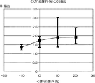
さらに、図7は、図3の長溝34の長さPL/振動腕36の長さである溝長さの割合Nを61.5パーセントとした場合において、振動腕36の腕幅縮幅率Mである振動腕の最大幅(W2)/最小幅(W1)の値を横軸にとり、縦軸にCI値比をとったグラフである。
図示するように、腕幅縮幅率Mを大きくする程、CI値比が大きくなり、好ましい。この実施形態では、振動腕36の腕幅縮幅率Mを1.06よりも大きくすることにより、CI値比を1より大きくすることができ、高調波による発振を防止することができる。
かくして、圧電振動片32において、振動腕の腕幅の幅縮幅率としての最大幅/最小幅=Mの値が、振動腕の腕長さに対する長溝の長さの割合=Nとの関係で決定されることにより、圧電振動片32やこれを搭載した圧電デバイス30を小型化しつつ、CI値を低減し、しかも高調波で発振しにくくして、良好な振動特性を実現することができる。
Further, FIG. 7 shows an arm width reduction ratio M of the vibrating
As shown in the figure, the larger the arm width reduction ratio M, the greater the CI value ratio, which is preferable. In this embodiment, by making the arm width reduction ratio M of the vibrating
Thus, in the piezoelectric vibrating
また、図8は図3の右側に拡大して示した第1の縮幅部TLの幅寸法とCI値の関係を図示したものである。
この場合、第1の縮幅部の高さ寸法THは50μm程度として、幅TWを横軸にとり、縦軸に示すCI値の変化を記録している。
図示されているように、TWが小さいとCI値が高く、TWが大きくなると歪みが小さくなって、図13で説明したZ方向の振動成分が減少し、振動が安定することで、CI値が小さくなる。図示されているように、この場合には、TWが0つまり、全く第1の縮幅部を形成しない状態から、この第1の縮幅部を設けてTWを10μm程度、特に11μm付近まで形成する場合に、CI値の顕著な減少が見られる。さらにTWの寸法が大きくされて、基部51の幅一杯まで増加させる間もCI値は徐々に減少する。
FIG. 8 illustrates the relationship between the width dimension of the first reduced width portion TL shown on the right side of FIG. 3 and the CI value.
In this case, the height dimension TH of the first reduced width portion is about 50 μm, the width TW is taken on the horizontal axis, and the change in the CI value shown on the vertical axis is recorded.
As shown in the figure, when the TW is small, the CI value is high, and when the TW is large, the distortion is small, the vibration component in the Z direction described with reference to FIG. 13 is reduced, and the vibration is stabilized. Get smaller. As shown in the figure, in this case, TW is 0, that is, the first reduced width portion is not formed at all, and the first reduced width portion is provided to form TW of about 10 μm, particularly around 11 μm. In this case, a significant decrease in CI value is observed. Further, the CI value gradually decreases while the dimension of the TW is increased to increase the base 51 to the full width.
以上述べたように、本実施形態によれば、圧電振動片32の各振動腕35,36の根本部分、すなわち、付け根付近が、第1の縮幅部により、剛性が強化されている。これにより、振動腕の屈曲振動を一層安定させることができCI値の抑制をはかることができる。
しかも、第2の縮幅部を設けたことで、振動腕36は、その付け根付近から、先端側に向かって、くびれ位置Pまで、徐々に剛性が低下し、くびれ位置Pからさらに先端側では、長溝34が無く、腕幅が徐々に拡大していることから、剛性は先端側にいくに従って高くされている。
このため、2次の高調波における振動の際の振動の「節」を、振動腕36のより先端側に位置させることができると考えられ、このことにより、長溝34を長くして圧電材料の電界効率を上げ、CI値を上昇させても、基本波のCI値を抑制しながら、2次の高調波のCI値の低下を招くことがないようにすることができる。かくして、小型化しても、基本波のCI値を低く抑えることができ、ドライブ特性が悪化することがない圧電振動片を提供することができる。
As described above, according to the present embodiment, the rigidity of the root portions of the vibrating
In addition, by providing the second reduced width portion, the
For this reason, it is considered that the “node” of vibration at the time of vibration in the second harmonic can be positioned on the more distal end side of the vibrating
次に、本実施形態の圧電振動片32の好ましい詳細構造について、図3および図4を参照しながら説明する。
図3に示す圧電振動片32の各振動腕35,36は同じ形状であるから、振動腕35と振動腕36のいずれかについて説明する事項は、両振動腕に共通する事項である。
図4の寸法xで示すウエハ厚み、すなわち、圧電振動片を形成する水晶ウエハの厚みは、70μmないし130μmが好ましい。
図3の寸法aで示す圧電振動片32の全長は、1300μmないし1600μm程度である。
振動腕の全長である寸法bは、1100ないし1400μmとし、1250μm程度が上述した理由により最も好ましい。
圧電デバイス30の基部幅である全幅dは、400μmないし600μm程度とすることが、圧電デバイスの小型化の上で好ましく、この実施形態では500μm程度である。このため、音叉部分の小型化のためには、基部51の先端側の幅寸法eは200ないし400μm程度である。
Next, a preferable detailed structure of the piezoelectric vibrating
Since the vibrating
The wafer thickness indicated by the dimension x in FIG. 4, that is, the thickness of the crystal wafer forming the piezoelectric vibrating piece is preferably 70 μm to 130 μm.
The total length of the piezoelectric vibrating
The dimension b which is the total length of the vibrating arm is 1100 to 1400 μm, and about 1250 μm is most preferable for the reason described above.
The total width d, which is the base width of the
また、図3の振動腕35と36の間の寸法kは、50ないし100μmとするのが好ましい。寸法kが50μmより少ないと、圧電振動片32の外形を、後述するように、水晶ウエハをウエットエッチングにより貫通させて形成する場合に、エッチング異方性に基づく異形部、すなわち、図4の符号81で示した振動腕側面におけるプラスX軸方向へのヒレ状凸部を、十分に小さくすることが困難になる。寸法kが100μm以上となると、振動腕の屈曲振動が不安定になるおそれがある。
さらに、図4の振動腕35(振動腕36も同じ)における長溝33の外縁と振動腕の外縁との寸法m1,m2は、ともに3ないし15μmとするとよい。寸法m1,m2は15μm以下とすることで、電界効率が向上し、3μm以上とすることで、電極の分極が確実に行われるのに有利である。
Also, the dimension k between the vibrating
Furthermore, the dimensions m1 and m2 of the outer edge of the
図3の振動腕36において、腕幅の変更点Pよりも先端側が拡幅している拡幅度合いが、振動腕36の腕幅が最小とされている箇所である該腕幅の変更点Pの箇所の幅に対して、0ないし20μm程度の増加とするのが好ましい。これを超えて拡幅されると、振動腕36の先端部が重くなりすぎて、屈曲振動の安定性を損なうおそれがある。
In the vibrating
また、図4における振動腕35(振動腕36も同じ)の外側の一側面に、プラスX軸方向にヒレ状に突出する異形部81が形成されている。これは、圧電振動片をウエットエッチングして外形形成する際に、水晶のエッチング異方性によりエッチング残りとして形成されるものであるが、好ましくは、フッ酸とフッ化アンモニウムによるエッチング液中で、9時間ないし11時間エッチングすることにより、該異形部81の突出量vを5μm以内に低減することが、振動腕35の安定した屈曲振動を得る上で好ましい。
Also, a
図3の寸法gで示す長溝の幅寸法は、振動腕の該長溝が形成されている領域において、振動腕の腕幅cに対して、60ないし90パーセント程度とするのが好ましい。振動腕35,36には、第1および第2の縮幅部が形成されているので、腕幅cは振動腕の長さ方向の位置によって異なるが、振動腕の最大幅に対して、長溝の幅gは60ないし90パーセント程度となる。これより長溝の幅が小さくなると、電界効率が下がり、CI値の上昇につながる。
The width dimension of the long groove indicated by dimension g in FIG. 3 is preferably about 60 to 90 percent of the arm width c of the vibrating arm in the region where the long groove of the vibrating arm is formed. Since the first and second reduced width portions are formed in the vibrating
さらに、図3の基部51の全長hは、圧電振動片32の全長aに対して、従来30パーセント程度あったものが、この実施形態は、切り込み部の採用などにより、15ないし25パーセント程度とすることができ、小型化を実現している。
Further, the total length h of the base 51 in FIG. 3 is conventionally about 30% with respect to the total length a of the piezoelectric vibrating
また、圧電振動片32の振動腕35,36が屈曲振動する際に、その振動漏れが伝えられる範囲について、振動腕の腕幅寸法cと相関があることに鑑み、本発明者等は、従来の圧電振動片の切り込み部が、適切な位置に設けられていないという知見を持った。そこで、図3の切り込み部71が設けられる位置について、前記振動腕の付け根から、前記振動腕の腕幅寸法cを超える寸法iの箇所としたものである。これによって、切り込み部71,71は、振動腕35,36からの振動漏れが、基部側に伝搬することを、より確実に抑制することができる構造とすることができる。これにより、振動腕側から基部側への振動の漏れ込みを適切に防止して、ドライブレベル特性が良好な圧電振動片を提供することができる。
特に、切り込み部71,71を、振動腕35,36の付け根の箇所Tから腕幅寸法c×1.2以上の寸法iだけ離して形成することで、ドライブレベル特性を正常な圧電振動片32のレベルに適合させることができることが確認されている。
また、長溝33,34の基部51側端部の位置は、図3において振動腕35,36の付け根、すなわちTの位置と同じか、それより僅かに振動腕先端側であって、第1の縮幅部TLが存在する範囲内であることが好ましく、特にTの位置よりも基部51の基端側に入り込まないようにすることが好ましい。
Further, in view of the fact that when the vibrating
In particular, the
In addition, the position of the end portion on the base 51 side of the
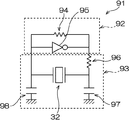
図9は、本実施形態の圧電振動片32を利用して圧電発振器を構成する場合の発振回路の例を示す回路図である。
発振回路91は、増幅回路92と帰還回路93を含んでいる。
増幅回路92は、増幅器95と帰還抵抗94を含んで構成されている。帰還回路93は、ドレイン抵抗96と、コンデンサ97,98と、圧電振動片32とを含んで構成されている。
ここで、図9の帰還抵抗94は、例えば10MΩ(メガオーム)程度、増幅器95はCMOSインバータを用いることができる。ドレイン抵抗96は、例えば200ないし900kΩ(キロオーム)、コンデンサ97(ドレイン容量)と、コンデンサ98(ゲート容量)は、それぞれ10ないし22pF(ピコファラド)とすることができる。
FIG. 9 is a circuit diagram illustrating an example of an oscillation circuit when a piezoelectric oscillator is configured using the piezoelectric vibrating
The
The amplifier circuit 92 includes an
Here, the
(圧電デバイスの製造方法)
次に、図10のフローチャートを参照しながら、上述の圧電デバイスの製造方法の一例を説明する。
圧電デバイス30の圧電振動片32と、パッケージ57と、蓋体40は、それぞれ別々に製造される。
(蓋体およびパッケージの製造方法)
蓋体40は、例えば、所定の大きさのガラス板(例えば、硼珪酸ガラス)を切断し、パッケージ57を封止するのに適合する大きさの蓋体として用意される。
パッケージ57は、上述したように、酸化アルミニウム質のセラミックグリーンシートを成形して形成される複数の基板を積層した後、焼結して形成されている。成形の際には、複数の各基板は、その内側に所定の孔を形成することで、積層した場合に内側に所定の内部空間Sを形成する。
(Piezoelectric device manufacturing method)
Next, an example of a method for manufacturing the above-described piezoelectric device will be described with reference to the flowchart of FIG.
The piezoelectric vibrating
(Method for manufacturing lid and package)
The
As described above, the
(圧電振動片の製造方法)
先ず、圧電基板を用意し、ひとつの圧電基板から所定数の圧電振動片について、同時にその外形をエッチングにより形成する(外形エッチング)。
ここで、圧電基板は、圧電材料のうち、例えば、圧電振動片32を複数もしくは多数分離することができる大きさの水晶ウエハが使用される。この圧電基板は工程の進行により図3の圧電振動片32を形成するので、図3に示すX軸が電気軸、Y軸が機械軸及びZ軸が光軸となるように、圧電材料、例えば水晶の単結晶から切り出されることになる。また、水晶の単結晶から切り出す際、上述のX軸、Y軸及びZ軸からなる直交座標系において、Z軸を中心に時計回りに0度ないし5度(図11のθ)の範囲で回転して切り出した水晶Z板を所定の厚みに切断研磨して得られる。
(Method for manufacturing piezoelectric vibrating piece)
First, a piezoelectric substrate is prepared, and the outer shape of a predetermined number of piezoelectric vibrating pieces is simultaneously formed by etching from one piezoelectric substrate (outer shape etching).
Here, as the piezoelectric substrate, for example, a quartz wafer having a size capable of separating a plurality or a large number of the piezoelectric vibrating
外形エッチングでは、図示しない耐蝕膜などのマスクを用いて、圧電振動片の外形から外側の部分として露出した圧電基板に関して、例えば、フッ酸溶液をエッチング液として、圧電振動片の外形のエッチングを行う。耐蝕膜としては、例えば、クロムを下地として、金を蒸着した金属膜などを用いることができる。このエッチング工程は、ウエットエッチングで、フッ酸溶液の濃度や種類、温度等により変化する。
ここで、外形エッチング工程でのウエットエッチングでは、図3に示した機械軸X、電気軸Y、光学軸Zに関して、エッチングの進行上、次のようなエッチング異方性を示す。
すなわち、圧電振動片32に関して、そのX−Y平面内におけるエッチングレートについては、プラスX方向で、このX軸に対して120度の方向、およびマイナス120度の方向の面内においてエッチングの進行が速く、マイナスX方向でX軸に対してプラス30度の方向、およびマイナス30度の方向の内面のエッチングの進行が遅くなる。
同様に、Y方向のエッチングの進行は、プラス30度方向およびマイナス30度方向が速くなり、プラスY方向で、Y軸に対してプラス120度方向、およびマイナス120度方向が遅くなる。
In the outer shape etching, the outer shape of the piezoelectric vibrating piece is etched using, for example, a hydrofluoric acid solution with respect to the piezoelectric substrate exposed as a portion outside the outer shape of the piezoelectric vibrating piece using a mask such as a corrosion-resistant film (not shown). . As the corrosion resistant film, for example, a metal film in which gold is vapor-deposited with chromium as a base can be used. This etching process is wet etching and changes depending on the concentration, type, temperature, and the like of the hydrofluoric acid solution.
Here, in the wet etching in the outer shape etching process, the following etching anisotropy is exhibited with respect to the mechanical axis X, the electric axis Y, and the optical axis Z shown in FIG.
That is, with respect to the piezoelectric vibrating
Similarly, the progress of etching in the Y direction is faster in the plus 30 degree direction and the minus 30 degree direction, and in the plus Y direction, the plus 120 degree direction and the minus 120 degree direction are delayed with respect to the Y axis.
このようなエッチング進行上の異方性により、圧電振動片32では、図4の符号81で示されているように、各振動腕の外側側面に、ヒレ状に突出した異形部が形成される。
しかしながら、この実施形態では、エッチング液として、フッ酸および、フッ化アンモニウムを用いて、十分な時間、すなわち、9時間ないし11時間という十分な時間をかけて、エッチングを行うことにより、図4で説明した異形部81をきわめて小さくすることができる(ST11)。
この工程において、圧電振動片32の切り込み部71,71を含む外形が形成され、終了時には、水晶ウエハに対して、それぞれ細い連結部で基部51付近を接続された多数の圧電振動片32の外形完成状態のものが得られる。
Due to such anisotropy in etching progress, the piezoelectric vibrating
However, in this embodiment, etching is performed using hydrofluoric acid and ammonium fluoride as an etchant for a sufficient time, that is, a sufficient time of 9 to 11 hours, so that in FIG. The described
In this process, the outer shape including the
(溝形成のためのハーフエッチング工程)
次に、図示しない溝形成用レジストにより、図4で示した形態となるように、各長溝を挟む両側の壁部を残す様にして、溝を形成しない部分に耐蝕膜を残し、外形エッチングと同じエッチング条件で、各振動腕35,36の表面と裏面を、それぞれウエットエッチングすることにより長溝に対応した底部を形成する(ST12)。
ここで、図4を参照すると、符号tで示す溝深さは、全体厚みxに対して、30ないし45パーセント程度とされる。tに関して、全体厚みxの30パーセント以下だと、電界効率を十分向上させることができない場合がある。45パーセント以上だと、剛性が不足して、屈曲振動に悪影響を与えたり、強度が不足する場合がある。
(Half etching process for groove formation)
Next, a groove forming resist (not shown) is used to form the shape shown in FIG. 4. Under the same etching conditions, the front and back surfaces of the vibrating
Here, referring to FIG. 4, the groove depth indicated by the symbol t is about 30 to 45 percent with respect to the total thickness x. If t is 30% or less of the total thickness x, the electric field efficiency may not be sufficiently improved. If it is 45% or more, the rigidity may be insufficient to adversely affect the bending vibration or the strength may be insufficient.
なお、上記外形エッチングおよび溝エッチングは、その一方もしくは両方を同時にドライエッチングにより形成してもよい。その場合には、例えば、圧電基板(水晶ウエハ)上に、圧電振動片32の外形や、外形形成後には、長溝に相当する領域を、その都度メタルマスクを配置して覆う。この状態で、例えば、図示しないチャンバー内に収容し、所定の真空度でエッチングガスを供給して、エッチングプラズマを生成しドライエッチングすることができる。つまり、真空チャンバー(図示せず)には、例えば、フレオンガスボンベと酸素ガスボンベとが接続され、さらに、真空チャンバーには、排気管が設けられ、所定の真空度に真空引きされるようになっている。
真空チャンバー内が、所定の真空度に真空排気され、フレオンガスと、酸素ガスが送られ、その混合ガスが所定の気圧になるまで充填された状態にて、直流電圧が印加されると、プラズマが発生する。そして、イオン化された粒子を含む混合ガスは、メタルマスクから露出した圧電材料に当たる。この衝撃により、物理的に削り取られて飛散し、エッチングが進行する。
Note that one or both of the outer shape etching and the groove etching may be simultaneously performed by dry etching. In that case, for example, on the piezoelectric substrate (crystal wafer), the outer shape of the piezoelectric vibrating
When a DC voltage is applied in a state where the inside of the vacuum chamber is evacuated to a predetermined degree of vacuum, a freon gas and an oxygen gas are sent, and the mixed gas is filled up to a predetermined atmospheric pressure, plasma is generated. appear. The mixed gas containing ionized particles hits the piezoelectric material exposed from the metal mask. Due to this impact, it is physically scraped off and scattered, and etching proceeds.
(電極形成工程)
次に、蒸着もしくはスパッタリングなどによって、電極となる金属、例えば、金を全面に被覆し、次いで、電極を形成しない箇所を露出したレジストを用いて、フォトリソグラフィの手法により、図1および図4で説明した駆動用の電極を形成する(ST13)。
その後、各振動腕35,36の先端部には、スパッタリングや蒸着により、錘付け電極(金属被膜)21,21が形成される(図3参照)(ST14)。錘付け電極21,21は通電されて圧電振動片32の駆動に用いられるのではなく、後述する周波数調整に利用される。
(Electrode formation process)
Next, a metal serving as an electrode, for example, gold is coated on the entire surface by vapor deposition or sputtering, and then a resist in which a portion where an electrode is not formed is exposed is exposed by a photolithography technique in FIGS. 1 and 4. The described driving electrode is formed (ST13).
Thereafter, weighting electrodes (metal coatings) 21 and 21 are formed on the tip portions of the vibrating
次いで、ウエハ上で、周波数の粗調整が行われる(ST15)。粗調整は、錘付け電極21,21の一部をレーザ光などのエネルギービームを照射することにより、部分的に蒸散させて、質量削減方式による周波数調整である。
続いて、上記したウエハに対する細い連結部を折り取り、圧電振動片32を個々に形成する個片にする(ST16)。
次に、図1で説明したように、パッケージ57の各電極部31,31に導電性接着剤43,43を塗布し、その上に圧電振動片32の基部51の引出し電極37a,38aの部分を載置して、接着剤を加熱・硬化させることにより、パッケージ57に対して、圧電振動片32を接合する(ST17)。
なお、この導電性接着剤43としては、例えば、合成樹脂などを利用したバインダー成分に、銀粒子などの導電粒子を混入したもので、機械的接合と電気的接続とを同時に行うことができるものである。
Next, rough adjustment of the frequency is performed on the wafer (ST15). Coarse adjustment is frequency adjustment by a mass reduction method by partially evaporating part of the
Subsequently, the thin connecting portion with respect to the wafer is broken, and the piezoelectric vibrating
Next, as described with reference to FIG. 1,
As the
続いて、蓋体40が金属製などの不透明な材料で形成されている場合には、図2で説明した貫通孔27は設けられていない。このため、蓋体40を接合する前に、圧電振動片32に対して、駆動電圧を印加して、周波数を見ながら、例えば、レーザ光を圧電振動片32の振動腕35および/または振動腕36の錘付け電極21の先端側に照射し、質量削減方式により微調整としての周波数調整を行う(ST18−1)。
次いで、シーム溶接などにより蓋体40をパッケージ57に接合し(ST19−1)、必要な検査を経て、圧電デバイス30が完成する。
Subsequently, when the
Next, the
あるいは、パッケージ57を透明な蓋体40で封止する場合には、圧電振動片32のST17における接合後において、該蓋体40をパッケージ57に接合する(ST18−2)。
この場合、例えば、低融点ガラスなどを加熱して、蓋体40をパッケージ57に接合する加熱工程が行われるが、この際に、低融点ガラスや導電性接着剤などからガスが生成される。そこで、加熱により、このようなガスを図2で説明した貫通孔27から排出し(脱ガス)、その後、段部29に金錫、より好ましくは、金ゲルマニウムなどでなる金属球体やペレットを配置し、レーザ光などを照射することにより、溶融する。これにより図2の金属充填材28が貫通孔27を気密に封止する(ST19−2)。
次いで、図2で示すように、硼珪酸ガラスなどでなる透明な蓋体40を透過させるように外部からレーザ光を圧電振動片32の振動腕35および/または振動腕36の錘付け電極21の先端側に照射し、質量削減方式により微調整としての周波数調整を行う(ST20−2)。次いで、必要な検査を経て、圧電デバイス30が完成する。
Alternatively, when the
In this case, for example, a heating step is performed in which the low melting point glass or the like is heated to join the
Next, as shown in FIG. 2, the laser beam is externally applied to the vibrating
本発明は上述の実施形態に限定されない。実施形態の各構成はこれらを適宜組み合わせたり、省略し、図示しない他の構成と組み合わせることができる。
また、この発明は、箱状のパッケージに圧電振動片を収容したものに限らず、シリンダー状の容器に圧電振動片を収容したもの、圧電振動片をジャイロセンサとして機能するようにしたもの、さらには、圧電振動子、圧電発振器等の名称にかかわらず、圧電振動片を利用したあらゆる圧電デバイスに適用することができる。
The present invention is not limited to the above-described embodiment. Each configuration of the embodiment can be appropriately combined or omitted, and can be combined with other configurations not shown.
The present invention is not limited to the case where the piezoelectric vibrating piece is accommodated in the box-shaped package, the case where the piezoelectric vibrating piece is accommodated in the cylindrical container, the piezoelectric vibrating piece functioning as a gyro sensor, Can be applied to any piezoelectric device using a piezoelectric vibrating piece regardless of the name of a piezoelectric vibrator, a piezoelectric oscillator, or the like.
30・・・圧電デバイス、32・・・圧電振動片、33,34・・・長溝、35,36・・・振動腕、TL・・・第1の縮幅部、CL・・・第2の縮幅部
DESCRIPTION OF
Claims (5)
前記基部と一体に形成され、前記基部の一端から延びる複数の振動腕と、
前記各振動腕の長手方向に沿って形成された長溝と、
前記長溝に形成した駆動用の電極とを備えており、
前記各振動腕は、該振動腕の前記基部に対する付け根の箇所から先端側に向かって縮幅する縮幅部を備え、
前記各縮幅部の先端に、前記振動腕の幅寸法が一定または増加に転じる幅変化の変更点Pがあり、前記変更点Pは、前記長溝の先端部よりもさらに振動腕の先端側に位置し、
前記各縮幅部は、第1の縮幅部と、前記第1の縮幅部の終端からさらに腕先端側に向かって縮幅する第2の縮幅部と、を備え、前記第1の縮幅部は前記第2の縮幅部より急激に縮幅する圧電振動片と、
前記圧電振動片の第1の端子が入力に接続され、前記圧電振動片の第2の端子が出力に接続されるCMOSインバータを用いた増幅器と、
を有することを特徴とする圧電発振器。 A base formed of piezoelectric material;
A plurality of vibrating arms formed integrally with the base and extending from one end of the base;
A long groove formed along the longitudinal direction of each vibrating arm;
An electrode for driving formed in the long groove,
Each of the vibrating arms includes a reduced width portion that is reduced in width toward a tip side from a base portion of the vibrating arm with respect to the base portion,
At the tip of each reduced width portion, there is a change point P of the width change in which the width dimension of the vibrating arm turns constant or increased, and the change point P is further on the tip side of the vibrating arm than the tip portion of the long groove. Position to,
Each of the reduced width portions includes a first reduced width portion, and a second reduced width portion that is further reduced in width from the end of the first reduced width portion toward the arm tip side. The reduced width portion is a piezoelectric vibrating piece that is reduced more rapidly than the second reduced width portion , and
An amplifier using a CMOS inverter in which a first terminal of the piezoelectric vibrating piece is connected to an input and a second terminal of the piezoelectric vibrating piece is connected to an output;
A piezoelectric oscillator comprising:
Priority Applications (5)
| Application Number | Priority Date | Filing Date | Title |
|---|---|---|---|
| JP2005129910A JP4301201B2 (en) | 2005-04-27 | 2005-04-27 | Piezoelectric oscillator |
| US11/234,741 US7368861B2 (en) | 2004-09-24 | 2005-09-23 | Piezoelectric resonator element and piezoelectric device |
| EP05020811A EP1641118B1 (en) | 2004-09-24 | 2005-09-23 | Piezoelectric resonator element and piezoelectric device |
| DE602005020725T DE602005020725D1 (en) | 2004-09-24 | 2005-09-23 | Piezoelectric resonator element and piezoelectric component |
| KR1020050088722A KR100712758B1 (en) | 2004-09-24 | 2005-09-23 | Piezoelectric resonator element and piezoelectric device |
Applications Claiming Priority (1)
| Application Number | Priority Date | Filing Date | Title |
|---|---|---|---|
| JP2005129910A JP4301201B2 (en) | 2005-04-27 | 2005-04-27 | Piezoelectric oscillator |
Publications (3)
| Publication Number | Publication Date |
|---|---|
| JP2006311090A JP2006311090A (en) | 2006-11-09 |
| JP2006311090A5 JP2006311090A5 (en) | 2008-03-13 |
| JP4301201B2 true JP4301201B2 (en) | 2009-07-22 |
Family
ID=37477476
Family Applications (1)
| Application Number | Title | Priority Date | Filing Date |
|---|---|---|---|
| JP2005129910A Expired - Fee Related JP4301201B2 (en) | 2004-09-24 | 2005-04-27 | Piezoelectric oscillator |
Country Status (1)
| Country | Link |
|---|---|
| JP (1) | JP4301201B2 (en) |
Families Citing this family (13)
| Publication number | Priority date | Publication date | Assignee | Title |
|---|---|---|---|---|
| US7764145B2 (en) * | 2006-11-30 | 2010-07-27 | Nihon Dempa Kogyo Co., Ltd. | Piezoelectric resonator, method of manufacturing the same and electronic part using the same |
| JP5353486B2 (en) * | 2009-06-30 | 2013-11-27 | セイコーエプソン株式会社 | Vibrating piece and vibrator |
| JP5789913B2 (en) * | 2010-02-05 | 2015-10-07 | セイコーエプソン株式会社 | Tuning fork type piezoelectric vibrating piece and piezoelectric device |
| JP5789914B2 (en) * | 2010-02-05 | 2015-10-07 | セイコーエプソン株式会社 | Tuning fork type piezoelectric vibrating piece and piezoelectric device |
| JP5760413B2 (en) * | 2010-12-08 | 2015-08-12 | セイコーエプソン株式会社 | Electronics |
| JP5671821B2 (en) * | 2010-03-16 | 2015-02-18 | セイコーエプソン株式会社 | Vibrating piece and device |
| US8304968B2 (en) | 2010-03-17 | 2012-11-06 | Seiko Epson Corporation | Vibrator element, vibrator, oscillator, and electronic apparatus |
| JP2012129904A (en) * | 2010-12-17 | 2012-07-05 | Seiko Epson Corp | Electronic apparatus |
| KR101532115B1 (en) * | 2011-12-01 | 2015-06-29 | 삼성전기주식회사 | Piezo vibrator and method for manufacturing the same |
| JP6115205B2 (en) * | 2013-03-13 | 2017-04-19 | セイコーエプソン株式会社 | Bending vibration piece, method for manufacturing bending vibration piece, vibration device, electronic apparatus, and moving body |
| JP2015149591A (en) * | 2014-02-06 | 2015-08-20 | セイコーエプソン株式会社 | Oscillation element, transducer, oscillator, electronic apparatus, sensor and mobile object |
| JP5696751B2 (en) * | 2013-08-29 | 2015-04-08 | セイコーエプソン株式会社 | Vibrating piece and vibrator |
| JP6375611B2 (en) * | 2013-11-16 | 2018-08-22 | セイコーエプソン株式会社 | Vibrating piece, vibrator, oscillator, electronic device and moving object |
-
2005
- 2005-04-27 JP JP2005129910A patent/JP4301201B2/en not_active Expired - Fee Related
Also Published As
| Publication number | Publication date |
|---|---|
| JP2006311090A (en) | 2006-11-09 |
Similar Documents
| Publication | Publication Date | Title |
|---|---|---|
| JP4415389B2 (en) | Piezoelectric device | |
| JP4301201B2 (en) | Piezoelectric oscillator | |
| JP4301200B2 (en) | Piezoelectric vibrating piece and piezoelectric device | |
| JP4442521B2 (en) | Piezoelectric vibrating piece and piezoelectric device | |
| JP4609196B2 (en) | Piezoelectric vibrating piece, piezoelectric device, electronic apparatus and mobile phone device | |
| KR100712758B1 (en) | Piezoelectric resonator element and piezoelectric device | |
| JP5115092B2 (en) | Piezoelectric vibrating piece, piezoelectric device, and oscillator | |
| JP2007096900A (en) | Piezoelectric vibrating piece and piezoelectric device | |
| JP2007258918A (en) | Piezoelectric device | |
| JP2007258917A (en) | Piezoelectric device | |
| JP4548148B2 (en) | Piezoelectric vibrating piece and piezoelectric device | |
| JP4207873B2 (en) | Piezoelectric vibrating piece and piezoelectric device | |
| JP2008048274A (en) | Piezo-electric vibrating piece and piezo-electric device | |
| JP2008022413A (en) | Piezoelectric vibration chip and piezoelectric device | |
| JP4784168B2 (en) | Piezoelectric vibrating piece and piezoelectric device | |
| JP2010004456A (en) | Piezoelectric vibrating piece and piezoelectric device | |
| JP5500220B2 (en) | Vibrating piece, vibrator, oscillator, and sensor | |
| JP2008048275A (en) | Piezoelectric vibrating piece and piezoelectric device | |
| JP2010246126A (en) | Piezoelectric vibration piece and piezoelectric device | |
| JP5045822B2 (en) | Piezoelectric vibrating piece and piezoelectric device | |
| JP2009232376A (en) | Method of manufacturing piezoelectric oscillator | |
| JP4222288B2 (en) | Piezoelectric vibrating piece and piezoelectric device |
Legal Events
| Date | Code | Title | Description |
|---|---|---|---|
| RD04 | Notification of resignation of power of attorney |
Free format text: JAPANESE INTERMEDIATE CODE: A7424 Effective date: 20070507 |
|
| RD03 | Notification of appointment of power of attorney |
Free format text: JAPANESE INTERMEDIATE CODE: A7423 Effective date: 20070509 |
|
| A521 | Request for written amendment filed |
Free format text: JAPANESE INTERMEDIATE CODE: A523 Effective date: 20070514 |
|
| A521 | Request for written amendment filed |
Free format text: JAPANESE INTERMEDIATE CODE: A523 Effective date: 20080130 |
|
| A977 | Report on retrieval |
Free format text: JAPANESE INTERMEDIATE CODE: A971007 Effective date: 20080417 |
|
| A131 | Notification of reasons for refusal |
Free format text: JAPANESE INTERMEDIATE CODE: A131 Effective date: 20080430 |
|
| A521 | Request for written amendment filed |
Free format text: JAPANESE INTERMEDIATE CODE: A523 Effective date: 20080627 |
|
| A131 | Notification of reasons for refusal |
Free format text: JAPANESE INTERMEDIATE CODE: A131 Effective date: 20081007 |
|
| A521 | Request for written amendment filed |
Free format text: JAPANESE INTERMEDIATE CODE: A523 Effective date: 20081205 |
|
| TRDD | Decision of grant or rejection written | ||
| A01 | Written decision to grant a patent or to grant a registration (utility model) |
Free format text: JAPANESE INTERMEDIATE CODE: A01 Effective date: 20090331 |
|
| A01 | Written decision to grant a patent or to grant a registration (utility model) |
Free format text: JAPANESE INTERMEDIATE CODE: A01 |
|
| FPAY | Renewal fee payment (event date is renewal date of database) |
Free format text: PAYMENT UNTIL: 20120501 Year of fee payment: 3 |
|
| R150 | Certificate of patent or registration of utility model |
Free format text: JAPANESE INTERMEDIATE CODE: R150 |
|
| A61 | First payment of annual fees (during grant procedure) |
Free format text: JAPANESE INTERMEDIATE CODE: A61 Effective date: 20090413 |
|
| FPAY | Renewal fee payment (event date is renewal date of database) |
Free format text: PAYMENT UNTIL: 20130501 Year of fee payment: 4 |
|
| FPAY | Renewal fee payment (event date is renewal date of database) |
Free format text: PAYMENT UNTIL: 20140501 Year of fee payment: 5 |
|
| LAPS | Cancellation because of no payment of annual fees |