JP4251286B2 - Display device - Google Patents
Display device Download PDFInfo
- Publication number
- JP4251286B2 JP4251286B2 JP2003560880A JP2003560880A JP4251286B2 JP 4251286 B2 JP4251286 B2 JP 4251286B2 JP 2003560880 A JP2003560880 A JP 2003560880A JP 2003560880 A JP2003560880 A JP 2003560880A JP 4251286 B2 JP4251286 B2 JP 4251286B2
- Authority
- JP
- Japan
- Prior art keywords
- substrate
- display device
- sealing
- wiring
- electrode
- Prior art date
- Legal status (The legal status is an assumption and is not a legal conclusion. Google has not performed a legal analysis and makes no representation as to the accuracy of the status listed.)
- Expired - Lifetime
Links
Images


Classifications
-
- H—ELECTRICITY
- H10—SEMICONDUCTOR DEVICES; ELECTRIC SOLID-STATE DEVICES NOT OTHERWISE PROVIDED FOR
- H10K—ORGANIC ELECTRIC SOLID-STATE DEVICES
- H10K50/00—Organic light-emitting devices
- H10K50/80—Constructional details
-
- H—ELECTRICITY
- H10—SEMICONDUCTOR DEVICES; ELECTRIC SOLID-STATE DEVICES NOT OTHERWISE PROVIDED FOR
- H10K—ORGANIC ELECTRIC SOLID-STATE DEVICES
- H10K59/00—Integrated devices, or assemblies of multiple devices, comprising at least one organic light-emitting element covered by group H10K50/00
- H10K59/10—OLED displays
- H10K59/12—Active-matrix OLED [AMOLED] displays
- H10K59/122—Pixel-defining structures or layers, e.g. banks
-
- H—ELECTRICITY
- H05—ELECTRIC TECHNIQUES NOT OTHERWISE PROVIDED FOR
- H05B—ELECTRIC HEATING; ELECTRIC LIGHT SOURCES NOT OTHERWISE PROVIDED FOR; CIRCUIT ARRANGEMENTS FOR ELECTRIC LIGHT SOURCES, IN GENERAL
- H05B33/00—Electroluminescent light sources
- H05B33/02—Details
- H05B33/04—Sealing arrangements, e.g. against humidity
-
- H—ELECTRICITY
- H10—SEMICONDUCTOR DEVICES; ELECTRIC SOLID-STATE DEVICES NOT OTHERWISE PROVIDED FOR
- H10K—ORGANIC ELECTRIC SOLID-STATE DEVICES
- H10K50/00—Organic light-emitting devices
- H10K50/80—Constructional details
- H10K50/84—Passivation; Containers; Encapsulations
- H10K50/841—Self-supporting sealing arrangements
-
- H—ELECTRICITY
- H10—SEMICONDUCTOR DEVICES; ELECTRIC SOLID-STATE DEVICES NOT OTHERWISE PROVIDED FOR
- H10K—ORGANIC ELECTRIC SOLID-STATE DEVICES
- H10K50/00—Organic light-emitting devices
- H10K50/80—Constructional details
- H10K50/84—Passivation; Containers; Encapsulations
- H10K50/842—Containers
- H10K50/8426—Peripheral sealing arrangements, e.g. adhesives, sealants
-
- H—ELECTRICITY
- H10—SEMICONDUCTOR DEVICES; ELECTRIC SOLID-STATE DEVICES NOT OTHERWISE PROVIDED FOR
- H10K—ORGANIC ELECTRIC SOLID-STATE DEVICES
- H10K50/00—Organic light-emitting devices
- H10K50/80—Constructional details
- H10K50/84—Passivation; Containers; Encapsulations
- H10K50/844—Encapsulations
- H10K50/8445—Encapsulations multilayered coatings having a repetitive structure, e.g. having multiple organic-inorganic bilayers
-
- H—ELECTRICITY
- H10—SEMICONDUCTOR DEVICES; ELECTRIC SOLID-STATE DEVICES NOT OTHERWISE PROVIDED FOR
- H10K—ORGANIC ELECTRIC SOLID-STATE DEVICES
- H10K59/00—Integrated devices, or assemblies of multiple devices, comprising at least one organic light-emitting element covered by group H10K50/00
- H10K59/10—OLED displays
- H10K59/12—Active-matrix OLED [AMOLED] displays
- H10K59/131—Interconnections, e.g. wiring lines or terminals
-
- H—ELECTRICITY
- H10—SEMICONDUCTOR DEVICES; ELECTRIC SOLID-STATE DEVICES NOT OTHERWISE PROVIDED FOR
- H10K—ORGANIC ELECTRIC SOLID-STATE DEVICES
- H10K59/00—Integrated devices, or assemblies of multiple devices, comprising at least one organic light-emitting element covered by group H10K50/00
- H10K59/80—Constructional details
- H10K59/88—Dummy elements, i.e. elements having non-functional features
Description
【技術分野】
【0001】
本発明は平面的なパネル型の表示装置に関し、特に、表示器周囲の非表示領域であるいわゆる額縁をより狭くすることを可能とした表示装置の発明に関する。
【背景技術】
【0002】
複数の表示素子を配列し、各表示素子の状態を制御することによって文字、画像、または映像などの画面を形成する表示装置が提供されている。例えば、液晶表示装置や有機EL表示装置などの電気光学装置が挙げられる。このような、表示装置においては、基板同士や基板と封止材との密閉を行って部材の劣化などを防止する。
【0003】
例えば、有機EL表示装置においては、装置内に侵入する周囲のガスが有機EL発光素子の寿命に影響を与える。特に、水分(水蒸気)や酸素は金属電極の劣化をもたらし、発光素子の長時間の動作を困難にしている。このため、有機EL表示素子のアレイを形成した基板をメタル缶や耐水性のプラスチックパッケージ、保護膜等によって密封して水蒸気や酸素に対するガスバリア性を得るようにしている。
【発明の開示】
【発明が解決しようとする課題】
【0004】
しかしながら、封止用メタル缶や封止用の保護膜等を表示素子を形成した表示素子基板上に形成する場合、封止用メタル缶や封止用の保護膜と表示素子基板とを接合するためのスペースが必要になる。また、上述したガスバリア性を確保するためには、一定の接合幅(接合スペース)も必要である。表示素子基板の封止はこの基板の外周で行われるため、外周には表示領域として利用されない、いわゆる額縁が生ずる。これは、表示装置を搭載する携帯電話機、携帯情報機器等の装置の小型化や自由なデザインを困難にする。
【0005】
よって、本発明は、額縁の領域をより狭くすることを可能とした表示装置を提供することを目的とする。
【0006】
また、本発明は、額縁の領域をより狭くしてもガスバリア性の低下しない表示装置を提供することを目的とする。
【課題を解決するための手段】
【0007】
上記目的を達成するため本発明の表示装置は、バンク層によって分離された複数の表示素子と配線層とを有する基板と、上記複数の表示素子と前記バンク層とを覆う電極層と、少なくとも上記基板の外周の封止領域で接合して上記基板を覆う封止基板と、を備え、上記配線層は上記基板の封止領域の一部に形成され、上記電極層の外周部は上記封止領域内にて上記配線層と接続される。
【0008】
かかる構成とすることによって、基板の封止領域の一部を電極と配線との接続領域として活用するので、ガスバリア等のために所要の接合幅を確保しつつ封止基板の外形を小さくすることができ、表示装置の額縁の構成要素となる部分のサイズを減らしている。
【0009】
好ましくは、上記電極層は各表示素子の共通電極(陰極や陽極)である。
【0010】
好ましくは、上記共通電極は上記表示素子側に位置する下層とその上に位置する上層の少なくとも2種類の電極層を含み、上記下層の電極層よりも上層の電極層がガスバリア性又は耐環境性が良い。それにより、下層の電極層の劣化を抑制することが可能となる。また、下層の電極層に発光効率(あるいは動作効率)が良い膜を使用することが可能となる。
【0011】
好ましくは、上記下層の電極層は上記複数の表示素子全体と上記バンク層の少なくとも一部とを覆うが、上記封止基板の外周側の封止部からは離間し、上記上層の電極は上記下部電極層全体を覆って上記封止基板の封止部内にまで至る。それにより、下層の電極層はガスが侵入する接合部から離間し、下層の電極層の劣化を抑制することが可能となる。また、下層の電極層に発光効率が良い膜を使用することが可能となる。
【0012】
好ましくは、上記封止基板の封止部は、上記基板に対向する面に該封止基板の外周を一周するように突起してな。それにより、中空の封止基板(断面凹型)で基板を封止することが可能となる。
【0013】
好ましくは、上記基板の(電源の)配線層の上面は平坦に形成され、この上に上記電極層が積層されて電気的に接続される。それにより、配線層と電極層との導通の確実が図られる。
【0014】
好ましくは、上記基板の上記封止基板の封止部に対向する面も平坦に形成される。それにより、基板の封止部分に加わる応力を均一にすることが可能となる。
【0015】
好ましくは、上記封止基板を多層薄膜に代えて封止を行う。それにより、可撓性のあるフィルム状の表示装置を実現可能となる。
【0016】
好ましくは、上記封止基板の封止部のサイズは、上記接合手段のガスバリア性又は耐環境性を確保するために必要なマージンによって決定され、このマージンに上記共通電極及びこの共通電極に電源を供給する配線層相互間を接続する接続領域が含まれる。それにより、信頼性の確保と表示装置の額縁の狭小化が可能となる。
【0017】
好ましくは、上記接合手段は接着膜を含み、この膜厚が20μmを越えないようになされる。また、上記接着膜の幅が少なくとも1mm以上である。それにより、外部雰囲気との接触面を小さくし、外部雰囲気の侵入長を大きくとって、封止された素子の劣化を抑制する。
【0018】
好ましくは、上記封止基板の外周は、上記基板に上記封止基板を載置する際のマージン分だけ上記基板の外周よりも内側に位置する。それにより、封止基板の基板への載置を容易にする。
【0019】
また、好ましくは、上記封止基板の外周、少なくとも上記基板を分割する際のスクライブマージン分だけ上記基板の外周よりも内側に位置する。それにより、組立後の表示器の分離切断の所要スペースを確保する。
【0020】
好ましくは、上記封止基板は平坦な基板によって構成される。それにより、より簡易に封止を行うことが可能となる。
【0021】
好ましくは、上記バンク層は上記封止基板の封止部内に位置しない。それにより、バンク層は封止部領域から離間するため、バンク層を相対的に水分の透過率の高い有機材料にて形成することが可能となる。
【0022】
好ましくは、上記表示素子の基板は多角形若しくは四角形であり、この基板の1辺で上記電極層の外周部と上記電源の配線層とが接続される。それにより、他辺(又は3辺)では電極層との配線の引き回しが不要となるので、該他辺(又は3辺)部分を狭額縁化することが可能となる。このような構成は、携帯電話機の表示装置のように、ある方向にはモジュールが延びても良いが、それ以外の方向では規制されるような場合に有効である。
【0023】
好ましくは、上記基板は多角形若しくは四角形であり、この基板の対向する2辺で前記電極層の外周部と前記電源の配線層とがそれぞれ接続される。このような構成は、電極までの配線抵抗を減少すると共に大容量の表示を行うために多数のドライバICを実装する場合等に有効である。
【0024】
好ましくは、上記基板は多角形若しくは四角形であり、この基板を囲む3辺で上記電極層の外周部と上記電源の配線層とが接続される。このような構成は、3辺で接続することによって電極までの配線抵抗を十分に低減させ、1辺で外部回路との接続を図ることができる。モジュール全体がバランス良く狭額縁化される。
【0025】
好ましくは、上記基板は多角形若しくは四角形であり、この基板を囲む4辺で上記電極層の外周部と上記電源の配線層とが接続される。このような構成は、大型の高精細表示装置を実現する場合に必要となる、配線抵抗を極力抵抗を下げる場合に好適である。この場合、電源配線層の下に絶縁膜を介して引き出し配線を形成し、あるいは、電極層と電源配線層との接続領域を複数のブロックに分け、ブロック相互間にまとめて引き出し配線を配置することとしても良い。
【0026】
好ましくは、上記複数の表示素子が配列された領域の外周にダミーの表示素子が配置される。それにより、表示に使用されないダミーの表示画素からガスが侵入するようにして、表示素子への実質的な影響を軽減する。また、インクジェット方式による表示素子の材料の塗布(塗布量)の均一化を図ることが可能となる。
【0027】
好ましくは、上記表示素子は有機EL素子である。上記下層の電極層はカルシウム、上記上層の電極層はアルミニウムである。
【0028】
好ましくは、上記バンク層は樹脂材料によって形成される。表示素子間にバンク層が存在することによって混色が防止される。
【0029】
好ましくは、上述した表示装置はデジタルカメラ、パーソナルコンピュータ、平面型テレビ、携帯情報端末装置、携帯電話装置、電子ブック等の電子機器に使用される。それにより、表示器の周囲に余分な非表示領域(額縁)の少ない各種装置類が得られる。
【0030】
本発明の表示装置の製造方法は、電気回路を形成すべき基板の外周内側の封止領域の一部に少なくとも配線層を形成する過程と、上記基板の前記配線層上を除いて複数の表示素子を相互に分離するための複数の溝を備える素子分離層を形成する過程と、上記素子分離層の複数の溝の各々に上記表示素子を形成する過程と、上記複数の表示素子と、上記素子分離層と、上記配線層各々の上に共通電極層を形成する過程と、上記基板の封止領域に接合材料を塗布する接合材料塗布過程と、上記基板の封止領域に環状の封止部を有する封止基板を前記接合材料を介して接合して上記基板を封止する封止過程と、を含む。
【0031】
かかる構成とすることによって、表示装置の額縁を狭くすることが可能となる。
【0032】
好ましくは、上記接合材料塗布過程は、上記基板の封止領域内に形成された前記共通電極層と前記配線層との接続領域上及び残り(この領域以外)の封止領域に接合材料を塗布する。それにより、基板と封止基板との間の封止領域を所要の接合材料で密封する。
【0033】
また、本発明の表示装置の製造方法は、電気回路を形成すべき基板の外周内側の封止領域の一部に少なくとも配線層を形成する過程と、上記基板の上記配線層上を除いて複数の表示素子を相互に分離するための複数の溝を備える素子分離層を形成する過程と、上記素子分離層の複数の溝の各々に上記表示素子を形成する過程と、上記複数の表示素子と、上記素子分離層と、上記配線層各々の上に共通電極層を形成する過程と、上記基板の封止領域及び上記共通電極層の上に接合材料を塗布する接合材料塗布過程と、上記基板に上記封止領域及び上記共通電極層を覆う封止基板を上記接合材料を介して接合して上記基板を封止する封止過程と、を含む。
【0034】
かかる構成とすることによって、表示装置の額縁を狭くすることが可能となる。
【0035】
また、表示装置の製造方法は、電気回路を形成すべき基板の外周内側の封止領域の一部に少なくとも配線層を形成する過程と、上記基板の上記配線層上を除いて複数の表示素子を相互に分離するための複数の溝を備える素子分離層を形成する過程と、上記素子分離層の複数の溝の各々に上記表示素子を形成する過程と、上記複数の表示素子と、上記素子分離層と、上記配線層各々の上に共通電極層を形成する過程と、上記基板に上記封止領域及び上記共通電極層を覆う多層膜を形成して上記基板を封止する封止過程と、を含む。
【0036】
好ましくは、上記多層膜は、水又はガスの透過を妨げる膜を含む。
【0037】
好ましくは、上記共通電極層は上記表示素子側に位置する下層とその上に位置する上層の少なくとも2種類の電極層を含み、上記下層の電極層よりも上層の電極層がガスバリア性又は耐環境性が良い。それにより、発光素子の劣化を防止可能とする。
【0038】
好ましくは、上記下層の電極層は上記複数の表示素子全体と上記バンク層の少なくとも一部とを覆うが、上記封止基板の封止部から離間し、上記上層の電極は上記下部電極層全体を覆って上記封止基板の封止部内にまで至る。それにより、下層の電極層の劣化を防止可能とする。
【発明を実施するための最良の形態】
【0039】
以下、本発明の実施の形態について図面を参照して説明する。
【0040】
図1乃至図3は、本発明の表示装置の第1の実施例を説明する説明図である。図1は、表示装置を概略的に示す平面図である。図2は、図1のA−B方向の断面を概略的に示す断面図である。図3は、図1のC−D方向の断面を概略的に示す断面図である。各図において対応する部分には同一部号を付している。なお、図2においては中央部の表示素子領域が簡略化されて示されている。
【0041】
実施例1の表示装置1は有機EL表示装置の例を示している。この表示装置1は、大別して、発光素子アレイを備えるTFT基板100、発光素子アレイを封止する封止基板200、TFT基板100と封止基板200とを接合する接合手段301、TFT基板100の走査線を駆動する走査線ドライバ部140、TFT基板100のデータ線を駆動するデータドライバIC401等によって構成される。
【0042】
TFT基板100は、マトリクス状に配列された複数の有機EL発光素子120と、これ等の発光素子120を駆動したり、スイッチとして機能するTFTトランジスタ130などによって構成されている。TFT基板100は、ガラス基板101上に保護膜102を形成し、この上にシリコンを堆積し、低濃度の不純物を注入してパターニングを行ってポリシリコンのTFT領域103を形成している。なお、基板100は樹脂基板であっても良い。この上にCVD法によって酸化シリコンによるゲート絶縁膜104を堆積している。この上にアルミニウムをスパッタ法によって堆積し、パターニングを行って、有機EL駆動用電源配線膜105及び106、有機EL用陰極配線膜107、TFT130のゲート配線膜108を形成している。次に、マスクを用いてTFT領域103のソース・ドレイン領域に高濃度のイオン注入を行い、酸化シリコンを堆積して第1の層間絶縁膜110を形成する。コンタクトホールのマスクを用いて異方性エッチングを行い、TFT領域103にコンタクトホールを開口する。次に、アルミニウムを堆積し、パターニングを行ってソース・ドレイン電極109、接続用電極112を形成する。次に、酸化シリコンを堆積して第2の層間絶縁膜111を形成する。金属イオンや水などTFTの劣化因子のTFTへの到達を抑制するために、第2の層間絶縁膜として、例えば、ホウ素、炭素、窒素、アルミニウム、ケイ素、リン、イッテルビウム、サマリウム、エルビウム、イットリウム、ガドリニウム、ジスプロシウム、ネオジウム、などの元素から選ばれた少なくとも1つの元素を含む絶縁膜も使用可能である。この上に後述の表示素子群を形成する。
【0043】
上述のように構成されたTFT基板100の中央部領域が表示素子群が配置された表示領域となっている。表示素子としての赤発光、緑発光、青発光の発光素子120は、これ等3色を一画素としてマトリクス状に配列されている。発光素子120各々の各放射光はガラス基板101を介して外部に放射される。なお、TFT基板100と反対側から光を取り出すこともできる。この場合、発光層より上層は光透過性の高い部材で構成することが好ましい。各発光素子を分離して混色を防止するために、各発光素子間及び表示領域の外周にバンク層113が形成されている。バンク層113は、例えば、フォトレジスト等の有機材料膜をパターニングすることによって形成することができる。
【0044】
発光素子120は、透明電極(ITO)の陽極121、有機EL層・正孔輸送層122、陰極(共通電極)123等によって構成される。陰極123は2層構造になっており、例えば、下層はカルシウム膜123a、上層はアルミニウム膜123bである。陰極123aは、各発光素子120と、各発光素子120相互間のバンク層と、表示領域の周囲のバンク層113とに渡って形成され、上層の陰極123bとのコンタクトが確保されている。上層の陰極123bは配線膜としても機能し、図2に示すように、バンク層113の外縁部に沿って、封止部202の下部の領域で配線膜107と接続されている。上記のように、有機EL層・正孔輸送層122と接する陰極123aをカルシウム膜とすることによって発光効率を高め、上層のアルミニウム膜123bによってカルシウム膜123aの全体を覆って低抵抗の配線とガスバリア(腐食防止)とを図っている。なお、発光層(有機EL層・正孔輸送層)の上に更に電子注入層又は電子輸送層、または電子注入層と電子輸送層の積層体を配置する有機EL素子構成としても良い。
【0045】
このように構成された基板100の上面を断面逆凹部形状の封止基板200によって封止する。封止基板200は、例えば、金属、ガラス、セラミック、プラスチックなどによって構成され、板状の封止板201と、この封止板下面の外周囲に形成された突起状の封止部202と、封止板201の下面に取り付けられた乾燥剤(材)203とを備えている。乾燥剤203は内部に侵入した水蒸気や酸素ガスを吸着する。
【0046】
TFT基板100と封止基板200間には不活性ガスとしての窒素ガスが充填され、両基板100及び200は接合手段としての接着剤301を介して封止部202にて接合される。接着剤301は、熱硬化性、紫外線硬化性など適当なものを使用するが、特に、水蒸気などのガスの浸透性の低いものを使用する。
【0047】
図2に示すように、基板100には、封止基板200を置くためのマージンaが設けられている。また、封止基板200の封止部202の幅d、すなわち、基板100の封止領域dは、接着剤301がガスの浸透を防止するのに適当な幅(接着剤301のみの部分の幅bと上下配線の接続幅cとの和に略相当する)に設定されている。例えば、この幅(接着剤301の幅d)を1mm以上として外部雰囲気の侵入長を大きくとり、水蒸気や酸素ガスの接着層からの侵入を困難にする。また、接着剤301の膜厚を20μm以下とし、接着剤301と外部雰囲気との接触面を小さくしてガスの侵入を困難にする。そして、封止した内部の素子の劣化を抑制する。
【0048】
この封止部202の下部の領域内に上下接続幅cだけ陰極膜123bが入り込み、基板100の配線107とITO膜113、ソース・ドレイン電極膜112を介して接続される。
【0049】
図3に示すように、基板100のデータ線は基板端部の電極121に接続され、異方性導電膜303を介して配線テープ402と接続される。この配線テープの途中に各データ線を駆動するデータドライバIC401がボンディングされている。基板100の下部においても、封止部202内に陰極123が一部入り込んでいる。
【0050】
図4は、TFT基板100と封止基板200とのより一般的な接合例(比較例)を示している。同図において図2と対応する部分には同一符号を付し、かかる部分の説明は省略する。
【0051】
この例では、封止基板200をTFT基板100に載置する際の載置マージンaと、ガスの浸透を阻止して封止の信頼性を確保するための接着剤301のマージンdとが陰極123と基板配線107との接続領域cの外側で確保されている。TFT基板100の端から接続領域cまでの寸法は、載置マージンa+接着剤301のマージンd+接続領域cとなっている。この構成では、表示装置1の外周の非表示領域の面積が大きくなっている。
【0052】
これに対して、図2に示す実施例1の構成では、封止部202の下部領域(幅d)に陰極123あるいは陰極123と配線107との接続領域cが入り込んでいる。TFT基板100の端から接続領域までの寸法は、載置マージンa+接着剤301のマージンdとなっている。接着剤301のマージンdは略b+cとなり、配線接続部分のマージンcの分だけ、非表示領域の面積が減少する。
【0053】
また、実施例1の構成では、封止部202の下部の領域が、図5(a)及び同(b)に示すように、可及的に平坦になるように、あるいは段差が変化しないように形成されている。図5(a)及び同(b)において、図2と対応する部分には、同一符号を付し、かかる部分の説明は省略する。
【0054】
図5(a)及び同(b)において、xは電源配線107と共通電極膜123との接続の幅、yは電源配線107と共通電極膜123とのずれ、zは当該接続領域の外周の封止領域下の封止マージンを示している。
【0055】
同図に示されるように、封止部202下部領域の、TFT基板100の電源配線107を比較的幅広にかつ平坦に形成する。電源配線107は、図1に示すように、他の配線と交差しないように基板100の外周に配置されている。それにより、配線同士の交差によって生ずる段差の発生をなるべく回避して、電源配線膜107が平坦に形成されるようにしている。この上に、アルミニウム膜112、ITO膜121を平坦に形成し、これ等の導電膜の平坦面1の上に更に、共通電極膜123のアルミニウムを堆積して発光素子120の陰極と電気的に接続している。この接続領域の外周側の基板100の上面(絶縁膜111)mも平坦に形成されている。
【0056】
好ましくは、図5(b)に示すように、電源配線107と共通電極膜123とのずれyが0となるようにする。それにより、電源配線107の幅と共通電極123の接続幅とを一致させて配線抵抗を最小とし、また、幅方向の寸法の無駄を省く。
【0057】
このように、電源配線膜107と共通電極123との導通部分(上下導通部分)xを平坦に形成し、この外周の封止領域zも平坦領域とする。上下導通を確実に行い、共通電極膜123形成後の膜端部の段差を均一に形成して、上下導通部分の高さをTFT基板100側で揃えて、封止条件が上下導通領部分で変化しないようにしている。更に、上下導通部xの外周部zに平坦部分zを確保することによって、缶封止によって封止部分に加わる応力を均一にすることが可能となる。
【0058】
図6(a)乃至同図(d)は、第1の実施例に係る表示装置1の製造プロセスを説明する工程図である。同図において、図2と対応する部分には、同一符号を付している。
【0059】
まず、図6(a)に示すように、TFT基板100を形成する。すなわち、ガラス基板101上にCVD法によってシリコン窒化膜を堆積して保護膜102を形成する。この上にCVD法によってシリコンを堆積する。更に、低濃度の不純物を注入してレーザアニールによる熱処理を行ってポリシリコン膜103を形成する。このポリシリコン膜のパターニングを行ってTFT領域130を形成する。この上にCVD法によって酸化シリコンによるゲート絶縁膜104を堆積している。この上にアルミニウムをスパッタ法によって堆積し、パターニングを行って、有機EL駆動用電源配線膜105及び106、有機EL用陰極配線膜107、TFT130のゲート配線膜108を形成する。次に、マスクを用いてTFT領域103のソース・ドレイン領域に高濃度のイオン注入を行い、熱処理によって不純物を活性化させる。更に、CVD法によって酸化シリコンを堆積して第1の層間絶縁膜110を形成する。この層間絶縁膜110にマスクを用いて異方性エッチングを行い、TFT領域103のソース・ドレイン領域にコンタクトホールを開口する。次に、アルミニウムを堆積し、パターニングを行ってソース・ドレイン電極109、接続用電極112を形成する。
【0060】
次に、図6(b)に示すように、CVD法によって酸化シリコンを堆積して第2の層間絶縁膜111を形成する。配線膜107上の層間絶縁膜111をエッチングしてアルミニウム膜112を露出させる。この上に、スパッタ法によってITOを堆積し、パターニングして発光素子の120の陽極121を形成する。また、配線膜上107のアルミニウム膜112上にもITO膜121を堆積し、接続領域の膜厚を調整するとともにアルミニウム表面が酸化されるのを防止する。
【0061】
図6(c)に示すように、感光性の有機樹脂膜をスピンコート法によって塗布し、パターニングを行って、発光素子の陽極(ITO)121を溝の底部に露出したバンク層113を形成する。このバンク層113は、各発光素子を分離する。次に、インクジェット法によって陽極121の上に、EL層122を形成する。EL層122は、例えば、発光層、電子輸送層、電子注入層、正孔注入層、正孔輸送層などによって構成される。これ等発光素子120の上に、例えば、カルシウム123aを真空蒸着してパターニングし、更にアルミニウム123bを蒸着してパターニングを行う。カルシウム123a及びアルミニウム123bは発光素子120の陰極(共通電極)123を構成する。陰極123を下層のカルシウム膜123aを上層のアルミニウム膜123bによって被覆する2層構造とすることによって、カルシウム膜123aへの水分の侵入を防止(ガスバリア性の確保)する。アルミニウム膜123bは共通電極123として基板101の外周にまで広がっており、外周部でITO膜121、アルミニウム膜112を介して配線膜107と、配線接続部分のマージンc(図2参照)にて接続される。
【0062】
次に、図6(d)に示すように、TFT基板100の外周の配線膜107を含む部分に接着剤あるいは封止剤301を塗布し、外周に突起部202が形成された逆凹形状の封止基板200を窒素ガス等の不活性ガス雰囲気中で張り合わせる。封止基板200内部に乾燥剤が配置されており、内部に侵入した水分や酸素を吸着する。接着剤301としては、酸素や水分を透過しない、絶縁性の材料が望ましく、光硬化性樹脂や熱硬化性樹脂を使用可能である。例えば、エポキシ系樹脂、アクリレート系樹脂の使用が可能である。
【0063】
このようにして、表示装置が形成される。
【0064】
図7及び図8は第2の実施例を示している。両図において図2及び図3と対応する部分には同一符号を付し、かかる部分の説明は省略する。
【0065】
この実施例では、封止基板200として平坦な基板を使用している。封止基板200は、例えば、ガラス板、アルミニウム板、ステンレス板、アクリル板、セラミック板などを適宜に使用可能である。TFT基板100と封止基板200との隙間を全て接着剤301で埋設して両基板を接合(接着)している。この場合においても、陰極123と基板の配線膜107との接続領域を含めて上述した封止の信頼性を確保するために必要なマージンb+cの幅を確保すると共に、この陰極123と基板の配線膜107との接続領域の内側にバンク層113が位置するようになされている。それにより、額縁の幅を狭くし、接着剤301から比較的に水分の透過率の高い樹脂膜113を隔離してバンク層113へのガスの侵入を防止する。
【0066】
図9(a)乃至同(d)は、第2の実施例の表示装置1の製造工程を説明する工程図である。同図において、図6と対応する部分には同一符号を付し、係る部分の説明は省略する。
【0067】
この表示装置においても、図9(a)乃至図9(c)の工程は、図6(a)乃至同図(c)と同様に行われる。
【0068】
図9(c)に示すように、TFT基板100が形成された後、スピンコート法あるいはインクジェット法、転写ローラなどによって接着剤301が適当な膜厚となるようにTFT基板100の上面に塗布される。この接着剤の膜の上に、封止基板200をTFT基板100に対して位置合わせを行いながら、張り合わせる。
【0069】
なお、封止基板200に接着剤301を塗布してTFT基板100と張り合わせても良い。また、封止基板200とTFT基板100とを合わせた後、周囲の隙間から毛細管現象によって接着剤を内部に浸透させることとしても良い。
【0070】
図10及び図11は、第3の実施例を示している。両図において図2及び図3と対応する部分には同一符号を付し、かかる部分の説明は省略する。
【0071】
この実施例では、封止基板200に代えて多層薄膜210を形成している。例えば、特開2000−223264では、無機パシベーション封止膜と樹脂封止膜との積層膜を封止膜として提案している。多層薄膜210は、TFT基板100の上に形成され、陰極123全体を覆っている。多層薄膜は、有機層/無機層/有機層の構成、または無機層/有機層/無機層の構成など種々の構成を採用することが可能である。無機材料としては、例えば、SiO2,SiN,SiONなどのセラミック材料等を、有機樹脂層としては、例えば、ポリエチレン、ポリスチレン、ポリプロピレンなどの、一般的な炭化水素系高分子を使用可能である。また、含フッ素系高分子でもよい。ポリマー材料そのものを配置することも、前駆体またはモノマーを基材上に塗布して硬化させてもよい。陰極123は、基板100の端部側で電源の配線107と接続されている。この例においても、陰極123と基板の配線膜107との接続領域を含めて上述した封止の信頼性を確保するために必要なマージンb+cの幅を確保すると共に、この陰極123と基板の配線膜107との接続領域の内側にバンク層113が位置するようになされている。それにより、額縁の幅を狭くしている。
【0072】
図12(a)乃至図12(d)は、第3の実施例の表示装置1の製造工程を説明する工程図である。同図において、図6と対応する部分には同一符号を付し、係る部分の説明は省略する。
【0073】
この表示装置においても、図12(a)乃至図12(c)の工程は、図6(a)乃至同図(c)と同様に行われる。
【0074】
図12(c)に示すように、TFT基板100が形成された後、図12(d)に示されるように、陰極123が外気に曝されないように、機密性の高い保護膜210でTFT基板100を覆い、外周をパターニングして基板を分離可能とする。保護膜210は、好ましくは、多層薄膜とする。前述したように、多層薄膜は、有機層/無機層/有機層を積層することにより、あるいは、無機層/有機層/無機層を積層すること等によって形成される。無機材料としては、例えば、SiO2,SiN,SiONなどのセラミック材料膜を、有機樹脂層としては、例えば、ポリエチレン、ポリスチレン、ポリプロピレンなどの、一般的な炭化水素系高分子を使用する。また、含フッ素系高分子でもよい。ポリマー材料そのものを配置することも、前駆体またはモノマーを基材上に塗布して硬化させてもよい。
【0075】
図13は、本発明の第4の実施例を示している。この実施例では、上述した第1乃至第3の実施例の表示装置の表示領域に、更に、ダミー画素を追加するようにした例を示している。
【0076】
表示装置内に侵入したガスは、膜内を浸透して表示領域の外周側の表示素子から影響を与える。そこで、予め画像表示に使用されないダミー画素を表示領域の外周に設けることで、侵入ガスの画面表示への影響を軽減する。また、表示領域の外周にダミー画素を設けることで、インクジェット法によって発光体材料を塗布する場合に塗布膜の均一化が図られる。すなわち、インクジェット法では、ノズルから微小なインク(材料)滴を吐出するが、吐出開始後、吐出量が安定するまである時間を必要とする。ダミー画素部分で吐出量を安定させることで各発光素子の塗布膜を均一化させることが可能となる。
【0077】
なお、発光体の形成にインクジェット法の代わりにマスク蒸着法を使用しても良い。また、インクジェット法とマスク蒸着法とを組み合わせて使用しても良い。
【0078】
図14乃至図17は、本発明の更に他の実施例を示している。各図において、図1と対応する部分には同一符号を付し、かかる部分の説明は省略する。
【0079】
これ等の実施例では、TFT基板と封止基板とを張り合わせて基板の外周を封止しているが、TFT基板の外周のいずれかの辺あるいは全ての辺で狭額縁化を図っている。
【0080】
図1及び図2に示した実施例では、図14に示すように、四角形(多角形)基板100の3辺(上辺、左辺、右辺)で電源配線107と共通電極(陰極)123とを接続し、それ等の外側領域で封止を行って狭額縁化を図り、1辺(下辺)で配線テープ402を使用してドライバIC(外部回路)と接続している。このようにすると、3辺接続で共通電極123までの配線抵抗を減らすことができ、1辺を外部回路接続に専用できるので、表示装置のモジュール全体をバランス良く、狭額縁化することが可能となる。
【0081】
図15に示す実施例では、基板100の1辺(下辺)で電源配線107と共通電極(陰極)123とを接続し、その外側領域で封止を行っている。この例では、1辺のみで共通電極123と配線膜107とを接続するので、この1辺で共通電極123と配線膜107間の十分な導通面積(上下導通面積)を確保しなければならないので狭額縁化は難しいが、それ以外の3辺では共通電極123との配線接続が不要であるので、3辺をかなり狭額縁化することができる。これは、ある方向にはモジュールが延びても良いが、それ以外の方向にはモジュールを延ばせないような場合、例えば、携帯電話機の表示装置などに都合の良い配置である。
【0082】
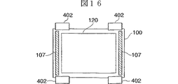
図16に示す実施例は、基板100の2辺(左辺、右辺)で共通電極123と配線膜107とを接続し、それ等の外側領域でそれぞれ封止を行っている。向かい合う両側(上辺、下辺)にそれぞれ配線テープ402を設けて外付け回路を実装する場合、例えば、奇数ラインは上から駆動し、偶数ラインは下から駆動するような場合に有効であり、多数のドライバICを実装して大容量(大画面)の表示を行うことが可能である。また、この構成では、図14に示した3辺で共通電極123と配線膜107とを接続した場合に匹敵する配線抵抗の低下を図ることが可能である。
【0083】
図17に示す実施例は、基板100の4辺(上辺、下辺、左辺、右辺)で共通電極123と配線膜107とを接続し、それ等の外側領域でそれぞれ封止を行っている。そして、多層配線膜によって共通電極123と配線膜107との導通を図る配線の下部に絶縁膜を介して引き出し配線を形成し、この配線を外部回路と接続している。なお、共通電極123と配線膜107とを接続する導通領域を複数のブロックに分け、ブロック相互間に引き出し配線を配置する構成とすることもできる。このような構成は、大型の高精細ディスプレイを実現する場合に必要となる、配線抵抗の十分な低減を可能とする。
【0084】
このように、本発明の各実施例によれば共通電極(陰極)123と基板配線107との接続領域(c)を封止マージン(b+c)内に含めて表示装置を組み立てるようにしているので、表示器の額縁の領域を減らすことが可能となる。
【0085】
また、共通電極123と基板配線107との接続領域(c)よりも基板の内側になるようにバンク層113を位置させるので、基板100と封止基板(あるいは封止膜)200との接合部分(b+c)からバンク層113内にガスが直接浸透することを回避可能となる。それにより、バンク層113として加工容易な樹脂(フォトレジストなど)を使用しても発光素子120への影響が少なくなる。
【0086】
また、カルシウム電極123aを陰極123aと基板配線107との接続領域(c)から離間させることによって酸素や水蒸気ガスの浸透によるカルシウム電極123aの腐食を回避する。
【0087】
次に、上述した本発明の表示装置を備えた電子機器の例について以下に説明するが、例示のものに限定されるものではない。
【0088】
〈モバイル型コンピュータ〉
まず、上述した実施形態に係る表示装置をモバイル型のパーソナルコンピュータに適用した例について説明する。図18は、このパーソナルコンピュータの構成を示す斜視図である。同図において、パーソナルコンピュータ1100は、キーボード1102を備えた本体部1104と、上述した表示装置1106を備えた表示装置ユニットとから構成されている。
【0089】
〈携帯電話〉
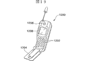
次に、上述した実施形態に係る表示装置を、携帯電話の表示部に適用した例について説明する。図19は、この携帯電話の構成を示す斜視図である。同図において、携帯電話1200は、複数の操作ボタン1202の他、受話口1024、送話口1206と共に上述した表示装置1208を備えるものである。
【0090】
〈ディジタルスチルカメラ〉
上述した実施形態に係る表示装置をファインダに用いたディジタルスチルカメラについて説明する。図20は、このディジタルスチルカメラの構成を示す斜視図であるが、外部機器との接続についても簡易に示すものである。
【0091】
通常のカメラは、被写体の光像によってフィルムを感光するのに対し、ディジタルスチルカメラ1300は、被写体の光像をCCD(Charge Coupled Device)等の撮像素子により光電変換して撮像信号を生成する。ディジタルスチルカメラ1300のケース1302の背面には、上述した表示装置1304が設けられ、CCDによる撮像信号に基づいて表示を行う構成となっている。このため、表示装置1304は、被写体を表示するファインダとして機能する。また、ケース1302の観察側(図においては裏面側)には、光学レンズやCCD等を含んだ受光ユニットが設けられている。
【0092】
撮影者が表示装置1304に表示された被写体を像を確認して、シャッタボタン1308を押すと、その時点におけるCCDの撮像信号が、回路基板1310のメモリに転送・格納される。また、このディジタルスチルカメラ1300は、ケース1302の側面に、ビデオ信号出力端子1312と、データ通信用の入出力端子1314とを備えている。そして、同図に示されるように、ビデオ信号出力端子1312にはテレビモニタ1430が、また、データ通信用の入出力端子1314にはパーソナルコンピュータ1430が、それぞれ必要に応じて接続され、更に、所定の操作によって、回路基板1308のメモリに格納された撮像信号が、テレビモニタ1330や、コンピュータ1340に出力される構成となっている。
【0093】
〈電子ブック〉
図21は、本発明の電子機器の一例としての電子ブックの構成を示す斜視図である。同図において、符号1400は、電子ブックを示している。電子ブック1400は、ブック型のフレーム1402と、このフレーム1402に開閉可能なカバー1403とを有する。フレーム1402には、その表面に表示面を露出させた状態で表示装置1404が設けられ、更に、操作部1405が設けられている。フレーム1402の内部には、コントローラ、カウンタ、メモリなどが内蔵されている。表示装置1404は、本実施形態では、表示素子を配置した画素部と、この画素部と一体に備えられ且つ集積化された周辺回路とを備える。周辺回路には、デコーダ方式のスキャンドライバ及びデータドライバを備える。
【0094】
なお、電子機器としては、図18のパーソナルコンピュータ、図19の携帯電話機、図20のディジタルスチルカメラ、図21の電子ブックの他にも、電子ペーパ、液晶テレビや、ビューファインダ型、モニタ直視型のビデオテープレコーダ、カーナビゲーション装置、ページャ、電子手帳、電卓、ワードプロセッサ、ワークステーション、テレビ電話、OS端末、タッチパネルを備えた機器などが挙げられる。そして、これ等の各種電子機器の表示部には、上述した表示装置が適用可能である。
【0095】
本発明の表示装置は実施例の有機EL表示装置に限られない。また、基板も実施例のTFT基板に限られない。アクティブ型のみならず、パッシブ型の基板にも本発明は適用可能である。
【0096】
また、実施例では、接合手段として接着剤を使用しているがこれに限られない。他の方法、例えば超音波やレーザによる接合を用いても良い。
【産業上の利用可能性】
【0097】
以上説明したように、本発明の表示装置によれば、表示領域の周囲の非表示領域である額縁の幅をより狭くすることが可能となって好ましい。
【図面の簡単な説明】
【0098】
【図1】図1は、本発明の表示装置の第1の実施例を説明する平面図である。
【図2】図2は、本発明の表示装置の第1の実施例(封止基板使用例)を説明する、図1のA−B部に沿った断面図である。
【図3】図3は、本発明の表示装置の第1の実施例を説明する、図1のC−D部に沿った断面図である。
【図4】図4は、第1の実施例の効果を説明するための、一般的な表示装置(比較例)の端部構造を説明する説明図である。
【図5】図5(a)及び同(b)は、基板外周の封止部における平坦性を説明する説明図であり、図5(a)は下地配線層121、112、107と共通電極123にずれがある場合を、同(b)はずれがない場合を示している。
【図6】図6は、第1の実施例の表示装置の製造工程を説明する工程図である。
【図7】図7は、本発明の表示装置の第2の実施例(封止基板全面接着例)を説明する、図1のA−B部に沿った断面図である。
【図8】図8は、本発明の表示装置の第2の実施例を説明する、図1のC−D部に沿った断面図である。
【図9】図9は、第2の実施例の表示装置の製造工程を説明する工程図である。
【図10】図10は、本発明の表示装置の第3の実施例(多層封止膜使用例)を説明する、図1のA−B部に沿った断面図である。
【図11】図11は、本発明の表示装置の第3の実施例を説明する、図1のC−D部の断面図である。
【図12】図12は、第3の実施例の表示装置の製造工程を説明する工程図である。
【図13】図13は、本発明の第4の表示装置の第4の実施例(ダミー画素使用例)を説明する平面図である。
【図14】図14は、基板の3辺で電源配線と共通電極との接続を行う例を説明する説明図である。
【図15】図15は、基板の1辺で電源配線と共通電極との接続を行う例を説明する説明図である。
【図16】図16は、基板の2辺で電源配線と共通電極との接続を行う例を説明する説明図である。
【図17】図17は、基板の4辺で電源配線と共通電極との接続を行う例を説明する説明図である。
【図18】図18は、本発明の表示装置を使用した携帯型のパーソナルコンピュータの例を説明する説明図である。
【図19】図19は、本発明の表示装置を使用した携帯型電話機の例を説明する説明図である。
【図20】図20は、本発明の表示装置を使用したデジタルカメラの例を説明する説明図である。
【図21】図21は、本発明の表示装置を使用した電子ブックの例を説明する説明図である。【Technical field】
[0001]
The present invention relates to a flat panel type display device, and more particularly to a display device invention that can make a so-called frame that is a non-display area around a display device narrower.
[Background]
[0002]
There has been provided a display device that forms a screen of characters, images, or images by arranging a plurality of display elements and controlling the state of each display element. For example, an electro-optical device such as a liquid crystal display device or an organic EL display device can be used. In such a display device, the substrates are sealed with each other and the substrate and the sealing material to prevent deterioration of the members.
[0003]
For example, in an organic EL display device, ambient gas that enters the device affects the life of the organic EL light emitting element. In particular, moisture (water vapor) and oxygen cause deterioration of the metal electrode, making it difficult to operate the light emitting element for a long time. For this reason, the substrate on which the array of organic EL display elements is formed is sealed with a metal can, a water-resistant plastic package, a protective film or the like to obtain a gas barrier property against water vapor or oxygen.
DISCLOSURE OF THE INVENTION
[Problems to be solved by the invention]
[0004]
However, when a sealing metal can, a sealing protective film, or the like is formed on a display element substrate on which a display element is formed, the sealing metal can or the sealing protective film is bonded to the display element substrate. Space is needed. Moreover, in order to ensure the gas barrier property mentioned above, a fixed joining width (joining space) is also required. Since the sealing of the display element substrate is performed on the outer periphery of the substrate, a so-called frame that is not used as a display area is generated on the outer periphery. This makes it difficult to downsize and freely design a device such as a mobile phone or a portable information device equipped with a display device.
[0005]
Therefore, an object of the present invention is to provide a display device capable of narrowing a frame area.
[0006]
Another object of the present invention is to provide a display device in which the gas barrier property does not deteriorate even if the frame region is narrowed.
[Means for Solving the Problems]
[0007]
In order to achieve the above object, a display device of the present invention includes a substrate having a plurality of display elements and a wiring layer separated by a bank layer, an electrode layer covering the plurality of display elements and the bank layer, and at least the above And a sealing substrate that covers the substrate by bonding at a sealing region on the outer periphery of the substrate, the wiring layer is formed in a part of the sealing region of the substrate, and the outer peripheral portion of the electrode layer is the sealing It is connected to the wiring layer in the region.
[0008]
With this configuration, a part of the sealing region of the substrate is used as a connection region between the electrode and the wiring, so that the outer shape of the sealing substrate can be reduced while securing a required bonding width for a gas barrier or the like. Therefore, the size of the part that constitutes the frame of the display device is reduced.
[0009]
Preferably, the electrode layer is a common electrode (cathode or anode) of each display element.
[0010]
Preferably, the common electrode includes at least two types of electrode layers, a lower layer positioned on the display element side and an upper layer positioned thereon, and the upper electrode layer is a gas barrier property or environmental resistance than the lower electrode layer. Is good. Thereby, deterioration of the lower electrode layer can be suppressed. In addition, it is possible to use a film having good light emission efficiency (or operation efficiency) for the lower electrode layer.
[0011]
Preferably, the lower electrode layer covers all of the plurality of display elements and at least a part of the bank layer, but is separated from the sealing portion on the outer peripheral side of the sealing substrate, and the upper electrode is It covers the entire lower electrode layer and reaches the sealing portion of the sealing substrate. As a result, the lower electrode layer is separated from the joint into which the gas enters, and deterioration of the lower electrode layer can be suppressed. In addition, it is possible to use a film having good luminous efficiency for the lower electrode layer.
[0012]
Preferably, the sealing portion of the sealing substrate protrudes from the surface facing the substrate so as to make one round of the outer periphery of the sealing substrate. Thereby, the substrate can be sealed with a hollow sealing substrate (concave concave).
[0013]
Preferably, the upper surface of the wiring layer (of the power supply) of the substrate is formed flat, and the electrode layer is laminated thereon and electrically connected. This ensures the conduction between the wiring layer and the electrode layer.
[0014]
Preferably, the surface of the substrate facing the sealing portion of the sealing substrate is also formed flat. Thereby, the stress applied to the sealing portion of the substrate can be made uniform.
[0015]
Preferably, sealing is performed by replacing the sealing substrate with a multilayer thin film. Thereby, a flexible film-like display device can be realized.
[0016]
Preferably, the size of the sealing portion of the sealing substrate is determined by a margin necessary to ensure the gas barrier property or environmental resistance of the joining means, and the common electrode and the power supply to the common electrode are used for the margin. A connection region for connecting the wiring layers to be supplied is included. As a result, reliability can be ensured and the frame of the display device can be narrowed.
[0017]
Preferably, the joining means includes an adhesive film, and the film thickness does not exceed 20 μm. The width of the adhesive film is at least 1 mm. Thereby, the contact surface with the external atmosphere is reduced, the penetration depth of the external atmosphere is increased, and deterioration of the sealed element is suppressed.
[0018]
Preferably, the outer periphery of the sealing substrate is positioned inside the outer periphery of the substrate by a margin when the sealing substrate is placed on the substrate. Thereby, the mounting of the sealing substrate on the substrate is facilitated.
[0019]
Preferably, the outer periphery of the sealing substrate is positioned on the inner side of the outer periphery of the substrate by at least a scribe margin when the substrate is divided. Thereby, a required space for separating and cutting the display after assembly is secured.
[0020]
Preferably, the sealing substrate is a flat substrate. Thereby, it becomes possible to perform sealing more simply.
[0021]
Preferably, the bank layer is not located in the sealing portion of the sealing substrate. Thereby, since the bank layer is separated from the sealing portion region, the bank layer can be formed of an organic material having a relatively high moisture permeability.
[0022]
Preferably, the substrate of the display element is a polygon or a rectangle, and the outer peripheral portion of the electrode layer and the wiring layer of the power source are connected to one side of the substrate. This eliminates the need for wiring with the electrode layer on the other side (or three sides), so that the other side (or three sides) can be narrowed. Such a configuration is effective when the module may extend in a certain direction, such as a display device of a mobile phone, but is restricted in other directions.
[0023]
Preferably, the substrate is polygonal or quadrangular, and the outer peripheral portion of the electrode layer and the wiring layer of the power source are respectively connected at two opposite sides of the substrate. Such a configuration is effective when, for example, a large number of driver ICs are mounted in order to reduce the wiring resistance to the electrodes and display a large capacity.
[0024]
Preferably, the substrate is polygonal or quadrangular, and the outer peripheral portion of the electrode layer and the wiring layer of the power source are connected at three sides surrounding the substrate. In such a configuration, the wiring resistance to the electrode can be sufficiently reduced by connecting at three sides, and connection to an external circuit can be achieved at one side. The entire module is narrowed with a good balance.
[0025]
Preferably, the substrate is a polygon or a rectangle, and the outer periphery of the electrode layer and the wiring layer of the power source are connected at four sides surrounding the substrate. Such a configuration is suitable for reducing the wiring resistance as much as possible, which is necessary when realizing a large high-definition display device. In this case, a lead-out wiring is formed under the power supply wiring layer via an insulating film, or the connection region between the electrode layer and the power-supply wiring layer is divided into a plurality of blocks, and the lead-out wiring is arranged between the blocks. It's also good.
[0026]
Preferably, a dummy display element is disposed on the outer periphery of the region where the plurality of display elements are arranged. Accordingly, gas is allowed to enter from dummy display pixels that are not used for display, thereby reducing the substantial influence on the display element. In addition, it is possible to make uniform the application (application amount) of the material of the display element by the ink jet method.
[0027]
Preferably, the display element is an organic EL element. The lower electrode layer is calcium, and the upper electrode layer is aluminum.
[0028]
Preferably, the bank layer is formed of a resin material. The presence of the bank layer between the display elements prevents color mixing.
[0029]
Preferably, the display device described above is used in an electronic device such as a digital camera, a personal computer, a flat-screen television, a portable information terminal device, a mobile phone device, and an electronic book. As a result, various devices having a small non-display area (frame) around the display can be obtained.
[0030]
The display device manufacturing method of the present invention includes a process of forming at least a wiring layer in a part of a sealing region inside an outer periphery of a substrate on which an electric circuit is to be formed, and a plurality of displays except for the wiring layer on the substrate. A process of forming an element isolation layer having a plurality of grooves for separating elements from each other; a process of forming the display element in each of the plurality of grooves of the element isolation layer; the plurality of display elements; Forming a common electrode layer on each of the element isolation layer, the wiring layer, a bonding material applying process for applying a bonding material to the sealing region of the substrate, and an annular sealing in the sealing region of the substrate; A sealing process in which a sealing substrate having a portion is bonded via the bonding material to seal the substrate.
[0031]
With this configuration, the frame of the display device can be narrowed.
[0032]
Preferably, in the bonding material application process, the bonding material is applied to the connection region between the common electrode layer and the wiring layer formed in the sealing region of the substrate and the remaining sealing region (other than this region). To do. Thereby, the sealing region between the substrate and the sealing substrate is sealed with a required bonding material.
[0033]
The display device manufacturing method according to the present invention includes a process of forming at least a wiring layer in a part of a sealing region inside the outer periphery of a substrate on which an electric circuit is to be formed, and a plurality of processes except for the wiring layer on the substrate. Forming a device isolation layer having a plurality of grooves for separating the display elements from each other, forming the display device in each of the plurality of grooves of the device isolation layer, and the plurality of display devices A process of forming a common electrode layer on each of the element isolation layer and the wiring layer, a bonding material applying process of applying a bonding material on the sealing region of the substrate and the common electrode layer, and the substrate And a sealing step of sealing the substrate by bonding a sealing substrate covering the sealing region and the common electrode layer through the bonding material.
[0034]
With this configuration, the frame of the display device can be narrowed.
[0035]
In addition, a method for manufacturing a display device includes a process of forming at least a wiring layer in a part of a sealing region inside an outer periphery of a substrate on which an electric circuit is to be formed, and a plurality of display elements except for the wiring layer on the substrate. Forming a device isolation layer having a plurality of grooves for separating each other, forming a display element in each of the plurality of grooves in the device isolation layer, the plurality of display devices, and the device A separation layer; a process of forming a common electrode layer on each of the wiring layers; and a sealing process of sealing the substrate by forming a multilayer film covering the sealing region and the common electrode layer on the substrate. ,including.
[0036]
Preferably, the multilayer film includes a film that prevents permeation of water or gas.
[0037]
Preferably, the common electrode layer includes at least two kinds of electrode layers, a lower layer positioned on the display element side and an upper layer positioned thereon, and the electrode layer above the lower electrode layer has a gas barrier property or environmental resistance. Good sex. Thereby, deterioration of the light emitting element can be prevented.
[0038]
Preferably, the lower electrode layer covers the whole of the plurality of display elements and at least a part of the bank layer, but is separated from the sealing portion of the sealing substrate, and the upper electrode is the entire lower electrode layer To the inside of the sealing portion of the sealing substrate. Thereby, deterioration of the lower electrode layer can be prevented.
BEST MODE FOR CARRYING OUT THE INVENTION
[0039]
Hereinafter, embodiments of the present invention will be described with reference to the drawings.
[0040]
1 to 3 are explanatory views for explaining a first embodiment of the display device of the present invention. FIG. 1 is a plan view schematically showing the display device. FIG. 2 is a cross-sectional view schematically showing a cross section in the direction AB of FIG. 3 is a cross-sectional view schematically showing a cross section in the CD direction of FIG. Corresponding parts are denoted by the same reference numerals in each figure. In FIG. 2, the central display element region is shown in a simplified manner.
[0041]
The
[0042]
The
[0043]
A central region of the
[0044]
The
[0045]
The upper surface of the
[0046]
Nitrogen gas as an inert gas is filled between the
[0047]
As shown in FIG. 2, the
[0048]
The
[0049]
As shown in FIG. 3, the data line of the
[0050]
FIG. 4 shows a more general bonding example (comparative example) between the
[0051]
In this example, the mounting margin a when the sealing
[0052]
On the other hand, in the configuration of the first embodiment shown in FIG. 2, the
[0053]
Further, in the configuration of the first embodiment, as shown in FIGS. 5A and 5B, the region below the sealing
[0054]
5A and 5B, x is a connection width between the
[0055]
As shown in the figure, the
[0056]
Preferably, as shown in FIG. 5B, the deviation y between the
[0057]
In this way, the conductive portion (vertical conductive portion) x between the power
[0058]
FIGS. 6A to 6D are process diagrams for explaining a manufacturing process of the
[0059]
First, as shown in FIG. 6A, a
[0060]
Next, as shown in FIG. 6B, silicon oxide is deposited by a CVD method to form a second
[0061]
As shown in FIG. 6C, a photosensitive organic resin film is applied by a spin coat method and patterned to form a
[0062]
Next, as shown in FIG. 6D, an adhesive or
[0063]
In this way, a display device is formed.
[0064]
7 and 8 show a second embodiment. In both figures, parts corresponding to those in FIGS. 2 and 3 are denoted by the same reference numerals, and description thereof will be omitted.
[0065]
In this embodiment, a flat substrate is used as the sealing
[0066]
FIGS. 9A to 9D are process diagrams for explaining a manufacturing process of the
[0067]
Also in this display device, the steps of FIGS. 9A to 9C are performed in the same manner as FIGS. 6A to 6C.
[0068]
As shown in FIG. 9C, after the
[0069]
Note that an adhesive 301 may be applied to the sealing
[0070]
10 and 11 show a third embodiment. In both figures, parts corresponding to those in FIGS. 2 and 3 are denoted by the same reference numerals, and description thereof will be omitted.
[0071]
In this embodiment, a multilayer
[0072]
12A to 12D are process diagrams for explaining a manufacturing process of the
[0073]
Also in this display device, the steps of FIG. 12A to FIG. 12C are performed in the same manner as FIG. 6A to FIG.
[0074]
As shown in FIG. 12C, after the
[0075]
FIG. 13 shows a fourth embodiment of the present invention. In this embodiment, an example is shown in which dummy pixels are further added to the display area of the display device of the first to third embodiments described above.
[0076]
The gas that has entered the display device penetrates the film and affects the display element on the outer peripheral side of the display area. Therefore, by providing dummy pixels that are not used for image display in advance on the outer periphery of the display area, the influence of intrusion gas on the screen display is reduced. Further, by providing dummy pixels on the outer periphery of the display area, the coating film can be made uniform when the phosphor material is applied by the ink jet method. That is, in the ink jet method, a minute ink (material) droplet is ejected from a nozzle, but a certain time is required until the ejection amount is stabilized after the ejection is started. By stabilizing the discharge amount at the dummy pixel portion, the coating film of each light emitting element can be made uniform.
[0077]
Note that a mask vapor deposition method may be used instead of the ink jet method for forming the light emitter. Moreover, you may use combining the inkjet method and a mask vapor deposition method.
[0078]
14 to 17 show still another embodiment of the present invention. In each figure, the same reference numerals are given to the portions corresponding to those in FIG. 1, and the description of such portions is omitted.
[0079]
In these embodiments, the outer periphery of the substrate is sealed by bonding the TFT substrate and the sealing substrate, but the frame is narrowed on any or all sides of the outer periphery of the TFT substrate.
[0080]
In the embodiment shown in FIGS. 1 and 2, as shown in FIG. 14, the
[0081]
In the embodiment shown in FIG. 15, the
[0082]
In the embodiment shown in FIG. 16, the
[0083]
In the embodiment shown in FIG. 17, the
[0084]
As described above, according to each embodiment of the present invention, the display device is assembled by including the connection region (c) between the common electrode (cathode) 123 and the
[0085]
Further, since the
[0086]
Further, by separating the
[0087]
Next, an example of an electronic apparatus including the above-described display device of the present invention will be described below, but is not limited to the example.
[0088]
<Mobile computer>
First, an example in which the display device according to the above-described embodiment is applied to a mobile personal computer will be described. FIG. 18 is a perspective view showing the configuration of this personal computer. In the figure, a
[0089]
<mobile phone>
Next, an example in which the display device according to the above-described embodiment is applied to a display unit of a mobile phone will be described. FIG. 19 is a perspective view showing the configuration of this mobile phone. In the figure, a
[0090]
<Digital still camera>
A digital still camera using the display device according to the above-described embodiment as a finder will be described. FIG. 20 is a perspective view showing the configuration of this digital still camera, but also shows a simple connection with an external device.
[0091]
A normal camera sensitizes a film with a light image of a subject, whereas a
[0092]
When the photographer confirms an image of the subject displayed on the
[0093]
<E-book>
FIG. 21 is a perspective view showing a configuration of an electronic book as an example of the electronic apparatus of the invention. In the figure,
[0094]
In addition to the personal computer shown in FIG. 18, the mobile phone shown in FIG. 19, the digital still camera shown in FIG. 20, and the electronic book shown in FIG. 21, the electronic equipment includes electronic paper, a liquid crystal television, a viewfinder type, and a monitor direct view type. Video tape recorders, car navigation devices, pagers, electronic notebooks, calculators, word processors, workstations, videophones, OS terminals, devices equipped with touch panels, and the like. And the display apparatus mentioned above is applicable to the display part of these various electronic devices.
[0095]
The display device of the present invention is not limited to the organic EL display device of the embodiment. Further, the substrate is not limited to the TFT substrate of the embodiment. The present invention can be applied not only to an active type but also to a passive type substrate.
[0096]
In the embodiment, an adhesive is used as the joining means, but the present invention is not limited to this. Other methods, for example, bonding by ultrasonic waves or lasers may be used.
[Industrial applicability]
[0097]
As described above, according to the display device of the present invention, it is preferable because the width of the frame, which is a non-display area around the display area, can be made narrower.
[Brief description of the drawings]
[0098]
FIG. 1 is a plan view for explaining a first embodiment of a display device of the present invention.
FIG. 2 is a cross-sectional view taken along a line AB in FIG. 1, for explaining a first embodiment (an example of using a sealing substrate) of a display device of the present invention.
FIG. 3 is a cross-sectional view taken along the line CD in FIG. 1 for explaining a first embodiment of the display device of the present invention.
FIG. 4 is an explanatory diagram for explaining an end structure of a general display device (comparative example) for explaining the effect of the first embodiment;
FIGS. 5A and 5B are explanatory views for explaining flatness in the sealing portion on the outer periphery of the substrate, and FIG. 5A shows the
FIG. 6 is a process diagram for explaining a manufacturing process for the display device according to the first embodiment;
FIG. 7 is a cross-sectional view taken along a line AB in FIG. 1 for explaining a second embodiment (an example of sealing substrate whole surface adhesion) of the display device of the present invention.
FIG. 8 is a cross-sectional view taken along the line CD in FIG. 1, for explaining a second embodiment of the display device of the present invention.
FIG. 9 is a process diagram for explaining a manufacturing process for the display device according to the second embodiment;
FIG. 10 is a cross-sectional view taken along the line AB of FIG. 1, for explaining a third embodiment (example of using a multilayer sealing film) of the display device of the present invention.
FIG. 11 11 These are sectional drawings of the CD section of
FIG. 12 is a process diagram for explaining a manufacturing process for the display device according to the third embodiment;
FIG. 13 is a plan view for explaining a fourth embodiment (an example of using dummy pixels) of the fourth display device of the present invention.
FIG. 14 is an explanatory diagram illustrating an example in which a power supply wiring and a common electrode are connected on three sides of a substrate.
FIG. 15 is an explanatory diagram illustrating an example in which a power supply wiring and a common electrode are connected on one side of a substrate.
FIG. 16 is an explanatory diagram illustrating an example in which a power supply wiring and a common electrode are connected on two sides of a substrate.
FIG. 17 is an explanatory diagram illustrating an example in which a power supply wiring and a common electrode are connected on four sides of a substrate.
FIG. 18 is an explanatory diagram illustrating an example of a portable personal computer using the display device of the present invention.
FIG. 19 is an explanatory diagram illustrating an example of a mobile phone using the display device of the present invention.
FIG. 20 is an explanatory diagram illustrating an example of a digital camera using the display device of the present invention.
FIG. 21 is an explanatory diagram illustrating an example of an electronic book using the display device of the present invention.
Claims (11)
前記基板上のうち、少なくとも前記基板の辺に沿った領域に配置された配線と、
前記基板上に配置された複数の第1電極と、
隣り合う前記第1電極の間に配置されたバンクを含むバンク層と、
前記複数の第1電極及び前記バンク層を覆う第2電極と、
前記第1電極と前記第2電極との間に配置された発光層と、
前記基板を覆う封止部材と、を備え、
前記第2電極と前記配線とは、前記基板のうち、前記基板の辺に沿って、かつ前記バンク層の外側のうち前記バンク層の外縁部に沿って設けられた接続領域において線状に電気的に接続される、ことを特徴とする表示装置。A substrate,
Wiring disposed on the substrate at least in a region along the side of the substrate;
A plurality of first electrodes disposed on the substrate;
A bank layer including a bank disposed between the adjacent first electrodes;
A second electrode covering the plurality of first electrodes and the bank layer;
A light emitting layer disposed between the first electrode and the second electrode;
A sealing member covering the substrate,
Wherein the wiring and the second electrode, wherein one of the substrate, along a side of the substrate, and electrically linearly on the connection area provided along the outer edge of the bank layer of the outer side of the bank layer A display device characterized by being connected to each other.
前記第2電極と前記配線とは、前記基板のうち、前記基板の少なくとも2辺に沿って前記バンク層の外側に設けられた前記接続領域において線状に電気的に接続される、ことを特徴とする表示装置。The display device according to claim 1,
The second electrode and the wiring are electrically connected linearly in the connection region provided outside the bank layer along at least two sides of the substrate among the substrates. Display device.
前記第2電極と前記配線とは、前記基板のうち、前記基板の少なくとも3辺に沿って前記バンク層の外側に設けられた前記接続領域において線状に電気的に接続される、ことを特徴とする表示装置。The display device according to claim 1,
The second electrode and the wiring are electrically connected in a line in the connection region provided outside the bank layer along at least three sides of the substrate among the substrates. Display device.
前記封止部材は、平坦な封止基板であり、
前記封止基板は、前記接続領域と一部が重なる封止領域に配置された接着剤を介して前記基板と接合されている、ことを特徴とする表示装置。The display device according to any one of claims 1 to 3,
The sealing member is a flat sealing substrate,
The display device, wherein the sealing substrate is bonded to the substrate through an adhesive disposed in a sealing region that partially overlaps the connection region.
前記封止基板は前記基板の封止領域に対向して該封止基板の外周を一周するように突起した封止部を含む、ことを特徴とする表示装置。The display device according to claim 4,
The display device, wherein the sealing substrate includes a sealing portion that protrudes so as to make a round of the outer periphery of the sealing substrate so as to face the sealing region of the substrate.
前記封止部材は、前記接続領域を覆うように形成された多層薄膜である、ことを特徴とする表示装置。The display device according to any one of claims 1 to 3,
The display device, wherein the sealing member is a multilayer thin film formed so as to cover the connection region.
前記第2電極は各表示素子の共通電極である、ことを特徴とする表示装置。The display device according to claim 1,
The display device, wherein the second electrode is a common electrode of each display element.
前記配線は該基板の外周側に形成された電源の配線層である、ことを特徴とする表示装置。The display device according to claim 1,
The display device, wherein the wiring is a power supply wiring layer formed on an outer peripheral side of the substrate.
前記バンク層は樹脂材料によって形成される、ことを特徴とする表示装置。The display device according to claim 1,
The display device, wherein the bank layer is formed of a resin material.
前記基板上に第1電極を形成する工程と、
前記基板上のうち隣り合う前記第1電極の間に配置されたバンクを含むバンク層を形成する工程と、
前記第1電極上に発光層を形成する工程と、
前記複数の第1電極及び前記バンク層を覆って第2電極を形成する工程と、
前記基板を封止部材により封止する工程と、を備え、
前記第2電極を形成する工程では、前記基板のうち、前記基板の辺に沿って、かつ前記バンク層の外側のうち前記バンク層の外縁部に沿って設けられた接続領域において、前記第2電極と前記配線とが線状に電気的に接続される、ことを特徴とする表示装置の製造方法。Forming a wiring in a region along at least the side of the substrate on the substrate;
Forming a first electrode on the substrate;
Forming a bank layer including a bank disposed between adjacent first electrodes on the substrate;
Forming a light emitting layer on the first electrode;
Forming a second electrode covering the plurality of first electrodes and the bank layer;
Sealing the substrate with a sealing member,
Wherein in the step of forming a second electrode, of said substrate, along a side of the substrate, and in the connection area provided along the outer edge of the bank layer of the outer side of the bank layer, the second A method for manufacturing a display device, wherein the electrode and the wiring are electrically connected in a linear shape.
Applications Claiming Priority (3)
| Application Number | Priority Date | Filing Date | Title |
|---|---|---|---|
| JP2002007337 | 2002-01-16 | ||
| JP2002007337 | 2002-01-16 | ||
| PCT/JP2003/000318 WO2003060858A1 (en) | 2002-01-16 | 2003-01-16 | Display device |
Related Child Applications (5)
| Application Number | Title | Priority Date | Filing Date |
|---|---|---|---|
| JP2005181577A Division JP4254752B2 (en) | 2002-01-16 | 2005-06-22 | Display device, electronic apparatus, and display device manufacturing method |
| JP2005181578A Division JP4701858B2 (en) | 2002-01-16 | 2005-06-22 | Organic electroluminescence device and electronic device |
| JP2008162863A Division JP5245566B2 (en) | 2002-01-16 | 2008-06-23 | Display device and electronic device |
| JP2008165626A Division JP4983734B2 (en) | 2002-01-16 | 2008-06-25 | Display device |
| JP2008257149A Division JP4983766B2 (en) | 2002-01-16 | 2008-10-02 | Display device |
Publications (2)
| Publication Number | Publication Date |
|---|---|
| JPWO2003060858A1 JPWO2003060858A1 (en) | 2005-05-19 |
| JP4251286B2 true JP4251286B2 (en) | 2009-04-08 |
Family
ID=19191321
Family Applications (9)
| Application Number | Title | Priority Date | Filing Date |
|---|---|---|---|
| JP2003560880A Expired - Lifetime JP4251286B2 (en) | 2002-01-16 | 2003-01-16 | Display device |
| JP2005181577A Expired - Lifetime JP4254752B2 (en) | 2002-01-16 | 2005-06-22 | Display device, electronic apparatus, and display device manufacturing method |
| JP2005181578A Expired - Lifetime JP4701858B2 (en) | 2002-01-16 | 2005-06-22 | Organic electroluminescence device and electronic device |
| JP2008162863A Expired - Lifetime JP5245566B2 (en) | 2002-01-16 | 2008-06-23 | Display device and electronic device |
| JP2008165626A Expired - Lifetime JP4983734B2 (en) | 2002-01-16 | 2008-06-25 | Display device |
| JP2008257149A Expired - Lifetime JP4983766B2 (en) | 2002-01-16 | 2008-10-02 | Display device |
| JP2009036206A Expired - Lifetime JP4983821B2 (en) | 2002-01-16 | 2009-02-19 | Display device |
| JP2011124164A Expired - Lifetime JP5299475B2 (en) | 2002-01-16 | 2011-06-02 | Display device and electronic device |
| JP2013004326A Expired - Lifetime JP5392424B2 (en) | 2002-01-16 | 2013-01-15 | Electro-optical device and electronic apparatus |
Family Applications After (8)
| Application Number | Title | Priority Date | Filing Date |
|---|---|---|---|
| JP2005181577A Expired - Lifetime JP4254752B2 (en) | 2002-01-16 | 2005-06-22 | Display device, electronic apparatus, and display device manufacturing method |
| JP2005181578A Expired - Lifetime JP4701858B2 (en) | 2002-01-16 | 2005-06-22 | Organic electroluminescence device and electronic device |
| JP2008162863A Expired - Lifetime JP5245566B2 (en) | 2002-01-16 | 2008-06-23 | Display device and electronic device |
| JP2008165626A Expired - Lifetime JP4983734B2 (en) | 2002-01-16 | 2008-06-25 | Display device |
| JP2008257149A Expired - Lifetime JP4983766B2 (en) | 2002-01-16 | 2008-10-02 | Display device |
| JP2009036206A Expired - Lifetime JP4983821B2 (en) | 2002-01-16 | 2009-02-19 | Display device |
| JP2011124164A Expired - Lifetime JP5299475B2 (en) | 2002-01-16 | 2011-06-02 | Display device and electronic device |
| JP2013004326A Expired - Lifetime JP5392424B2 (en) | 2002-01-16 | 2013-01-15 | Electro-optical device and electronic apparatus |
Country Status (7)
| Country | Link |
|---|---|
| US (7) | US7038377B2 (en) |
| EP (1) | EP1450334B1 (en) |
| JP (9) | JP4251286B2 (en) |
| KR (1) | KR100510421B1 (en) |
| CN (1) | CN1253839C (en) |
| TW (1) | TWI283142B (en) |
| WO (1) | WO2003060858A1 (en) |
Cited By (1)
| Publication number | Priority date | Publication date | Assignee | Title |
|---|---|---|---|---|
| US9012949B2 (en) | 2011-07-08 | 2015-04-21 | Semiconductor Energy Laboratory Co., Ltd. | Light-emitting module, light-emitting device, and method for manufacturing the light-emitting module |
Families Citing this family (121)
| Publication number | Priority date | Publication date | Assignee | Title |
|---|---|---|---|---|
| US7288420B1 (en) * | 1999-06-04 | 2007-10-30 | Semiconductor Energy Laboratory Co., Ltd. | Method for manufacturing an electro-optical device |
| US7444309B2 (en) * | 2001-10-31 | 2008-10-28 | Icosystem Corporation | Method and system for implementing evolutionary algorithms |
| JP2003332045A (en) * | 2002-05-09 | 2003-11-21 | Sanyo Electric Co Ltd | Electroluminescence display device and its manufacturing method |
| JP3778176B2 (en) * | 2002-05-28 | 2006-05-24 | セイコーエプソン株式会社 | LIGHT EMITTING DEVICE AND ELECTRONIC DEVICE |
| JP2003347044A (en) * | 2002-05-30 | 2003-12-05 | Sanyo Electric Co Ltd | Organic el panel |
| US7449246B2 (en) * | 2004-06-30 | 2008-11-11 | General Electric Company | Barrier coatings |
| JP3945525B2 (en) * | 2003-02-20 | 2007-07-18 | セイコーエプソン株式会社 | Electro-optic device |
| JP3791618B2 (en) * | 2003-02-20 | 2006-06-28 | セイコーエプソン株式会社 | ELECTRO-OPTICAL DEVICE, MANUFACTURING METHOD THEREOF, AND ELECTRONIC DEVICE |
| JP3906930B2 (en) * | 2003-02-20 | 2007-04-18 | セイコーエプソン株式会社 | ELECTRO-OPTICAL DEVICE, MANUFACTURING METHOD THEREOF, AND ELECTRONIC DEVICE |
| EP1611546B1 (en) | 2003-04-04 | 2013-01-02 | Icosystem Corporation | Methods and systems for interactive evolutionary computing (iec) |
| JP2005044613A (en) * | 2003-07-28 | 2005-02-17 | Seiko Epson Corp | Manufacturing method of light emitting device, and light emitting device |
| KR100544123B1 (en) * | 2003-07-29 | 2006-01-23 | 삼성에스디아이 주식회사 | Flat panel display |
| WO2005013081A2 (en) * | 2003-08-01 | 2005-02-10 | Icosystem Corporation | Methods and systems for applying genetic operators to determine system conditions |
| JP3915985B2 (en) * | 2003-08-22 | 2007-05-16 | セイコーエプソン株式会社 | Pixel element substrate, display device, electronic device, and manufacturing method of pixel element substrate |
| US7356518B2 (en) * | 2003-08-27 | 2008-04-08 | Icosystem Corporation | Methods and systems for multi-participant interactive evolutionary computing |
| KR100552972B1 (en) | 2003-10-09 | 2006-02-15 | 삼성에스디아이 주식회사 | Flat panel display and fabrication method thereof |
| JP4678124B2 (en) * | 2003-11-10 | 2011-04-27 | セイコーエプソン株式会社 | Electro-optical device, method of manufacturing electro-optical device, and electronic apparatus |
| CN1906650B (en) * | 2003-11-14 | 2012-05-09 | 株式会社半导体能源研究所 | Display device and its fabrication method |
| KR101146208B1 (en) | 2003-11-14 | 2012-05-25 | 가부시키가이샤 한도오따이 에네루기 켄큐쇼 | Liquid crystal display device and method for manufacturing the same |
| KR100600865B1 (en) | 2003-11-19 | 2006-07-14 | 삼성에스디아이 주식회사 | Electro luminescence display contained EMI shielding means |
| KR100611153B1 (en) | 2003-11-27 | 2006-08-09 | 삼성에스디아이 주식회사 | Plat panel display device |
| JP4899286B2 (en) * | 2004-01-30 | 2012-03-21 | セイコーエプソン株式会社 | ORGANIC EL DISPLAY DEVICE, ITS MANUFACTURING METHOD, AND ELECTRONIC DEVICE |
| JP4058695B2 (en) * | 2004-02-16 | 2008-03-12 | セイコーエプソン株式会社 | Electro-optical device and electronic apparatus |
| KR100615212B1 (en) | 2004-03-08 | 2006-08-25 | 삼성에스디아이 주식회사 | Flat display device |
| KR100581903B1 (en) | 2004-03-09 | 2006-05-22 | 삼성에스디아이 주식회사 | Electroluminescence display device |
| US7619258B2 (en) * | 2004-03-16 | 2009-11-17 | Semiconductor Energy Laboratory Co., Ltd. | Display device |
| US7764012B2 (en) * | 2004-04-16 | 2010-07-27 | Semiconductor Energy Laboratory Co., Ltd | Light emitting device comprising reduced frame portion, manufacturing method with improve productivity thereof, and electronic apparatus |
| US7707220B2 (en) * | 2004-07-06 | 2010-04-27 | Icosystem Corporation | Methods and apparatus for interactive searching techniques |
| US20060010117A1 (en) * | 2004-07-06 | 2006-01-12 | Icosystem Corporation | Methods and systems for interactive search |
| KR100698689B1 (en) * | 2004-08-30 | 2007-03-23 | 삼성에스디아이 주식회사 | Light emitting display and fabrication method thereof |
| US7527994B2 (en) * | 2004-09-01 | 2009-05-05 | Honeywell International Inc. | Amorphous silicon thin-film transistors and methods of making the same |
| US8350466B2 (en) * | 2004-09-17 | 2013-01-08 | Semiconductor Energy Laboratory Co., Ltd. | Display device and manufacturing method thereof |
| EP1655790B1 (en) * | 2004-10-21 | 2010-08-04 | LG Display Co., Ltd. | Organic electroluminescent device and method of manufacturing the same |
| TWI411349B (en) * | 2004-11-19 | 2013-10-01 | Semiconductor Energy Lab | Display device and electronic device |
| EP1724853B1 (en) * | 2005-05-17 | 2015-05-06 | LG Display Co., Ltd. | Organic electroluminescent device |
| EP1760798B1 (en) * | 2005-08-31 | 2012-01-11 | Semiconductor Energy Laboratory Co., Ltd. | Semiconductor device and manufacturing method thereof |
| EP1760776B1 (en) * | 2005-08-31 | 2019-12-25 | Semiconductor Energy Laboratory Co., Ltd. | Manufacturing method for semiconductor device with flexible substrate |
| EP1927058A4 (en) * | 2005-09-21 | 2011-02-02 | Icosystem Corp | System and method for aiding product design and quantifying acceptance |
| JP2007123240A (en) | 2005-09-28 | 2007-05-17 | Sony Corp | Manufacturing method of display device and display device |
| US7851996B2 (en) * | 2005-11-16 | 2010-12-14 | Canon Kabushiki Kaisha | Display apparatus |
| JP4827499B2 (en) * | 2005-11-16 | 2011-11-30 | キヤノン株式会社 | Current-driven device and display device |
| JP4736757B2 (en) * | 2005-12-01 | 2011-07-27 | セイコーエプソン株式会社 | LIGHT EMITTING DEVICE AND ELECTRONIC DEVICE |
| JP4742835B2 (en) * | 2005-12-05 | 2011-08-10 | セイコーエプソン株式会社 | LIGHT EMITTING DEVICE AND ELECTRONIC DEVICE |
| KR100673765B1 (en) | 2006-01-20 | 2007-01-24 | 삼성에스디아이 주식회사 | Organic light-emitting display device and the preparing method of the same |
| US8038495B2 (en) | 2006-01-20 | 2011-10-18 | Samsung Mobile Display Co., Ltd. | Organic light-emitting display device and manufacturing method of the same |
| KR100635514B1 (en) | 2006-01-23 | 2006-10-18 | 삼성에스디아이 주식회사 | Organic electroluminescence display device and method for fabricating of the same |
| KR100671647B1 (en) | 2006-01-26 | 2007-01-19 | 삼성에스디아이 주식회사 | Organic light emitting display device |
| KR100688792B1 (en) * | 2006-01-27 | 2007-03-02 | 삼성에스디아이 주식회사 | Flat panel display and method of the same |
| KR100759666B1 (en) * | 2006-01-27 | 2007-09-17 | 삼성에스디아이 주식회사 | Flat panel display and method of the same |
| JP5160754B2 (en) * | 2006-01-31 | 2013-03-13 | エルジー ディスプレイ カンパニー リミテッド | EL device |
| JP4533392B2 (en) * | 2006-03-22 | 2010-09-01 | キヤノン株式会社 | Organic light emitting device |
| JP4736890B2 (en) * | 2006-03-28 | 2011-07-27 | 大日本印刷株式会社 | Organic electroluminescence device |
| JP4864520B2 (en) * | 2006-04-12 | 2012-02-01 | 三菱電機株式会社 | Organic EL display device and method of manufacturing organic EL display device |
| KR100914784B1 (en) * | 2006-05-17 | 2009-08-31 | 엘지디스플레이 주식회사 | Light emitting device and fabrication method of the same |
| US7994709B2 (en) * | 2006-05-22 | 2011-08-09 | Koninklijke Philips Electronics N.V. | OLED device employing a metal thin-film connected to a high-current cable |
| KR101281888B1 (en) * | 2006-06-30 | 2013-07-03 | 엘지디스플레이 주식회사 | organic electro-luminescence display device and method for fabricating the same |
| JP2008047340A (en) * | 2006-08-11 | 2008-02-28 | Dainippon Printing Co Ltd | Organic electroluminescence device |
| JP4245032B2 (en) * | 2006-10-03 | 2009-03-25 | セイコーエプソン株式会社 | LIGHT EMITTING DEVICE AND ELECTRONIC DEVICE |
| US7792816B2 (en) * | 2007-02-01 | 2010-09-07 | Icosystem Corporation | Method and system for fast, generic, online and offline, multi-source text analysis and visualization |
| KR100830981B1 (en) * | 2007-04-13 | 2008-05-20 | 삼성에스디아이 주식회사 | Organic light emitting diode display |
| JP2008311059A (en) * | 2007-06-14 | 2008-12-25 | Rohm Co Ltd | Organic electroluminescent element and its manufacturing method |
| JP5208591B2 (en) * | 2007-06-28 | 2013-06-12 | 株式会社半導体エネルギー研究所 | Light emitting device and lighting device |
| JP4884320B2 (en) * | 2007-06-29 | 2012-02-29 | 京セラ株式会社 | Image display device |
| TW200915820A (en) * | 2007-09-19 | 2009-04-01 | Giga Byte Tech Co Ltd | Touch panel structure having dual touch-modes, and signal processing method and device |
| JP5119865B2 (en) * | 2007-11-02 | 2013-01-16 | セイコーエプソン株式会社 | Organic electroluminescence equipment, electronic equipment |
| KR101362164B1 (en) * | 2007-12-11 | 2014-02-12 | 엘지디스플레이 주식회사 | Organcic electro-luminescence dispaly and manufacturing method thereof |
| JP5163430B2 (en) * | 2008-01-09 | 2013-03-13 | セイコーエプソン株式会社 | Electro-optical device and electronic apparatus |
| CN101971235B (en) * | 2008-03-04 | 2013-09-18 | 夏普株式会社 | Display device substrate, method for manufacturing the same, display device, method for forming multi-layer wiring, and multi-layer wiring substrate |
| WO2010032329A1 (en) * | 2008-09-22 | 2010-03-25 | パイオニア株式会社 | El light emitting device |
| WO2010071089A1 (en) * | 2008-12-17 | 2010-06-24 | Semiconductor Energy Laboratory Co., Ltd. | Light-emitting device and electronic device |
| JP2010170776A (en) * | 2009-01-21 | 2010-08-05 | Konica Minolta Holdings Inc | Organic electroluminescent element and its manufacturing method |
| JP5190709B2 (en) * | 2009-02-20 | 2013-04-24 | カシオ計算機株式会社 | Display panel and manufacturing method thereof |
| KR20110019498A (en) * | 2009-08-20 | 2011-02-28 | 삼성모바일디스플레이주식회사 | Organic light emitting display device |
| JP5218460B2 (en) * | 2010-03-26 | 2013-06-26 | セイコーエプソン株式会社 | Pyroelectric detector, pyroelectric detector and electronic device |
| JP5471774B2 (en) | 2010-04-27 | 2014-04-16 | セイコーエプソン株式会社 | Electro-optical device, method of manufacturing electro-optical device, and electronic apparatus |
| KR101845480B1 (en) | 2010-06-25 | 2018-04-04 | 가부시키가이샤 한도오따이 에네루기 켄큐쇼 | Method for manufacturing semiconductor device |
| KR101201720B1 (en) * | 2010-07-29 | 2012-11-15 | 삼성디스플레이 주식회사 | Display device and organic light emitting diode display |
| DE102010032834B4 (en) * | 2010-07-30 | 2023-05-25 | Pictiva Displays International Limited | Optoelectronic device and method for its manufacture |
| KR20120028418A (en) * | 2010-09-14 | 2012-03-23 | 삼성모바일디스플레이주식회사 | Method for manufacturing encapsulated substrate using organic luminescence display device and encapsulated substrate using organic luminescence display device |
| JP5003808B2 (en) * | 2010-09-17 | 2012-08-15 | セイコーエプソン株式会社 | Electro-optical device and electronic apparatus |
| KR101757810B1 (en) * | 2010-11-19 | 2017-07-17 | 삼성디스플레이 주식회사 | Display device, organic light emitting diode display, and manufacturing method of sealing substrate |
| KR20120089108A (en) * | 2011-02-01 | 2012-08-09 | 삼성전기주식회사 | Touch panel |
| US8823659B2 (en) | 2011-06-07 | 2014-09-02 | Nokia Corporation | Method and apparatus for touch panel |
| KR20120138168A (en) * | 2011-06-14 | 2012-12-24 | 삼성디스플레이 주식회사 | Display device and method for manufacturing the same |
| CN103085437B (en) * | 2011-11-02 | 2016-04-06 | 宸鸿科技(厦门)有限公司 | Bonding structure, the electronic installation with this bonding structure and applying method thereof |
| JP5318182B2 (en) * | 2011-11-30 | 2013-10-16 | キヤノン株式会社 | Manufacturing method of organic EL element |
| JP2013235128A (en) * | 2012-05-09 | 2013-11-21 | Seiko Epson Corp | Manufacturing method of electro-optic device and substrate for electro-optic device |
| CN102800815B (en) * | 2012-08-06 | 2015-05-20 | 深圳市华星光电技术有限公司 | Display device and manufacturing method thereof |
| TWI559064B (en) | 2012-10-19 | 2016-11-21 | Japan Display Inc | Display device |
| JP6228735B2 (en) * | 2013-02-21 | 2017-11-08 | 株式会社ジャパンディスプレイ | Display device |
| KR101960388B1 (en) | 2012-12-24 | 2019-03-20 | 엘지디스플레이 주식회사 | Organic light emitting diode display device |
| KR101980766B1 (en) * | 2012-12-27 | 2019-05-21 | 엘지디스플레이 주식회사 | Organic light emitting diode display device including touch panel |
| JP6221386B2 (en) | 2013-06-18 | 2017-11-01 | セイコーエプソン株式会社 | LIGHT EMITTING DEVICE AND ELECTRONIC DEVICE |
| JP6217161B2 (en) * | 2013-06-19 | 2017-10-25 | セイコーエプソン株式会社 | LIGHT EMITTING DEVICE AND ELECTRONIC DEVICE |
| KR102079257B1 (en) | 2013-06-28 | 2020-02-20 | 삼성디스플레이 주식회사 | Thin film transistor array substrate and organic light emitting display including the substrate |
| KR20150011231A (en) * | 2013-07-22 | 2015-01-30 | 삼성디스플레이 주식회사 | Organic light emitting display apparatus and the manufacturing method thereof |
| KR20150021000A (en) | 2013-08-19 | 2015-02-27 | 가부시키가이샤 한도오따이 에네루기 켄큐쇼 | Display device |
| KR102117612B1 (en) | 2013-08-28 | 2020-06-02 | 삼성디스플레이 주식회사 | Organic light emitting display apparatus and the manufacturing method thereof |
| JP5981904B2 (en) * | 2013-11-15 | 2016-08-31 | 株式会社ナンシン | Caster mounting structure |
| CN110867469B (en) * | 2014-03-17 | 2023-12-29 | 三星显示有限公司 | Organic EL display device |
| CN104216159B (en) | 2014-09-03 | 2017-09-22 | 上海天马有机发光显示技术有限公司 | A kind of display panel and preparation method thereof, display device |
| TWI552334B (en) * | 2015-03-25 | 2016-10-01 | 友達光電股份有限公司 | Pixel structure of display panel |
| KR102442616B1 (en) * | 2015-04-08 | 2022-09-14 | 삼성디스플레이 주식회사 | Organic light-emitting display apparatus and manufacturing method thereof |
| WO2016204054A1 (en) * | 2015-06-16 | 2016-12-22 | シャープ株式会社 | Method for manufacturing display device, and display device |
| JP2017037172A (en) * | 2015-08-10 | 2017-02-16 | 株式会社ジャパンディスプレイ | Display |
| KR102554963B1 (en) | 2015-10-29 | 2023-07-11 | 엘지디스플레이 주식회사 | Organic light emitting display device |
| KR102502656B1 (en) * | 2015-12-15 | 2023-02-21 | 엘지디스플레이 주식회사 | Organic light emitting display device |
| JP6557601B2 (en) | 2015-12-29 | 2019-08-07 | 株式会社ジャパンディスプレイ | Display device and method for manufacturing display device |
| KR102605957B1 (en) * | 2016-02-23 | 2023-11-27 | 삼성디스플레이 주식회사 | Organic light emitting display device and method of manufacturing an organic light emitting display device |
| JP6714401B2 (en) * | 2016-03-18 | 2020-06-24 | 株式会社ジャパンディスプレイ | Display device |
| CN106293252B (en) * | 2016-09-09 | 2020-02-07 | 上海中航光电子有限公司 | Array substrate and display device |
| US10559772B2 (en) * | 2017-03-31 | 2020-02-11 | Sharp Kabushiki Kaisha | Display device and production method thereof |
| JP6912080B2 (en) * | 2017-06-09 | 2021-07-28 | 株式会社Joled | Organic EL display panel |
| US11765941B2 (en) * | 2017-12-26 | 2023-09-19 | Sharp Kabushiki Kaisha | Display device |
| KR102546170B1 (en) * | 2018-01-19 | 2023-06-22 | 삼성디스플레이 주식회사 | Display device |
| JP2019153551A (en) * | 2018-03-06 | 2019-09-12 | 株式会社ジャパンディスプレイ | Organic el display |
| US11502146B2 (en) | 2018-03-28 | 2022-11-15 | Sharp Kabushiki Kaisha | Display device with frame region including metal layers across slit |
| US10804491B2 (en) * | 2018-12-13 | 2020-10-13 | Wuhan China Star Optoelectronics Semiconductor Display Technology Co., Ltd. | Organic light emitting diode display device |
| EP4009373A4 (en) * | 2019-08-01 | 2022-08-17 | BOE Technology Group Co., Ltd. | Display substrate and display apparatus |
| JP7418077B2 (en) * | 2019-08-30 | 2024-01-19 | キヤノン株式会社 | Semiconductor devices, display devices, and electronic equipment |
| KR20220092098A (en) | 2020-12-24 | 2022-07-01 | 엘지디스플레이 주식회사 | Display apparatus |
Family Cites Families (69)
| Publication number | Priority date | Publication date | Assignee | Title |
|---|---|---|---|---|
| JPH0752668B2 (en) * | 1988-11-16 | 1995-06-05 | シャープ株式会社 | Thin film EL device |
| JPH04278983A (en) | 1991-03-07 | 1992-10-05 | Fuji Electric Co Ltd | Method for sealing display panel |
| NL194873C (en) * | 1992-08-13 | 2003-05-06 | Oki Electric Ind Co Ltd | Thin film transistors array and liquid crystal display device using it. |
| US5504390A (en) * | 1994-03-03 | 1996-04-02 | Topp; Mark | Addressable electroluminescent display panel having a continuous footprint |
| US6025901A (en) * | 1995-08-14 | 2000-02-15 | Sharp Kabushiki Kaisha | Liquid crystal display device and method for producing the same |
| JPH0982476A (en) * | 1995-09-14 | 1997-03-28 | Casio Comput Co Ltd | Organic electroluminescent element |
| JPH09148066A (en) * | 1995-11-24 | 1997-06-06 | Pioneer Electron Corp | Organic electroluminescent element |
| JPH1048654A (en) * | 1996-07-30 | 1998-02-20 | Nec Kagoshima Ltd | Terminal structure of lcd panel |
| JP4354019B2 (en) * | 1997-04-18 | 2009-10-28 | 出光興産株式会社 | Organic electroluminescence device |
| JPH10198285A (en) * | 1997-01-13 | 1998-07-31 | Toshiba Corp | Planar display device |
| KR100260611B1 (en) * | 1997-04-03 | 2000-07-01 | 윤종용 | Lcd panel for reparing lines |
| US6147724A (en) * | 1997-04-04 | 2000-11-14 | Hitachi, Ltd. | Back light system for minimizing non display area of liquid crystal display device |
| JP3541625B2 (en) * | 1997-07-02 | 2004-07-14 | セイコーエプソン株式会社 | Display device and active matrix substrate |
| JP3580092B2 (en) | 1997-08-21 | 2004-10-20 | セイコーエプソン株式会社 | Active matrix display |
| JP3830238B2 (en) * | 1997-08-29 | 2006-10-04 | セイコーエプソン株式会社 | Active matrix type device |
| KR100249784B1 (en) * | 1997-11-20 | 2000-04-01 | 정선종 | Encapsulation of the polymeric or organic light light emitting device using multiple polymer layers |
| JP2000003783A (en) * | 1998-06-12 | 2000-01-07 | Tdk Corp | Organic electroluminescent display device |
| JP2000173766A (en) | 1998-09-30 | 2000-06-23 | Sanyo Electric Co Ltd | Display device |
| JP3423232B2 (en) * | 1998-11-30 | 2003-07-07 | 三洋電機株式会社 | Active EL display |
| JP2000174282A (en) * | 1998-12-03 | 2000-06-23 | Semiconductor Energy Lab Co Ltd | Semiconductor device |
| JP3817081B2 (en) | 1999-01-29 | 2006-08-30 | パイオニア株式会社 | Manufacturing method of organic EL element |
| JP3549760B2 (en) * | 1999-02-18 | 2004-08-04 | シャープ株式会社 | Flat panel display |
| JP3670923B2 (en) * | 1999-02-26 | 2005-07-13 | 三洋電機株式会社 | Color organic EL display device |
| KR20020011392A (en) * | 1999-04-28 | 2002-02-08 | 메리 이. 보울러 | Flexible Organic Electronic Device with Improved Resistance to Oxygen and Moisture Degradation |
| JP2000315058A (en) * | 1999-04-30 | 2000-11-14 | Toshiba Corp | Array substrate for display device |
| JP4075028B2 (en) * | 1999-06-14 | 2008-04-16 | セイコーエプソン株式会社 | Circuit board, display device, and electronic device |
| JP2001078463A (en) * | 1999-09-06 | 2001-03-23 | Amada Co Ltd | High-frequency inverter with main switch overcurrent protecting circuit |
| CN1186683C (en) | 1999-09-08 | 2005-01-26 | 松下电器产业株式会社 | Display device and method of manufacture thereof |
| JP2001154218A (en) * | 1999-09-08 | 2001-06-08 | Matsushita Electric Ind Co Ltd | Display device and its manufacturing method |
| US6833668B1 (en) | 1999-09-29 | 2004-12-21 | Sanyo Electric Co., Ltd. | Electroluminescence display device having a desiccant |
| US6876145B1 (en) * | 1999-09-30 | 2005-04-05 | Semiconductor Energy Laboratory Co., Ltd. | Organic electroluminescent display device |
| JP2001102169A (en) | 1999-10-01 | 2001-04-13 | Sanyo Electric Co Ltd | El display |
| JP2001109395A (en) * | 1999-10-01 | 2001-04-20 | Sanyo Electric Co Ltd | El display device |
| JP2001109398A (en) * | 1999-10-04 | 2001-04-20 | Sanyo Electric Co Ltd | Display device |
| US6623861B2 (en) * | 2001-04-16 | 2003-09-23 | Battelle Memorial Institute | Multilayer plastic substrates |
| JP2001125509A (en) * | 1999-10-28 | 2001-05-11 | Nippon Seiki Co Ltd | Electroluminescence display device |
| US8957584B2 (en) | 1999-10-29 | 2015-02-17 | Semiconductor Energy Laboratory Co., Ltd. | Self light-emitting device |
| TW478019B (en) | 1999-10-29 | 2002-03-01 | Semiconductor Energy Lab | Self light-emitting device |
| JP4823413B2 (en) * | 1999-10-29 | 2011-11-24 | 株式会社半導体エネルギー研究所 | Self-luminous device |
| JP4727029B2 (en) * | 1999-11-29 | 2011-07-20 | 株式会社半導体エネルギー研究所 | EL display device, electric appliance, and semiconductor element substrate for EL display device |
| TW525122B (en) | 1999-11-29 | 2003-03-21 | Semiconductor Energy Lab | Electronic device |
| JP2001189190A (en) | 2000-01-06 | 2001-07-10 | Auto Network Gijutsu Kenkyusho:Kk | Organic el display device |
| TW480727B (en) * | 2000-01-11 | 2002-03-21 | Semiconductor Energy Laboratro | Semiconductor display device |
| JP2001195026A (en) * | 2000-01-14 | 2001-07-19 | Victor Co Of Japan Ltd | Matrix type display device |
| US6633121B2 (en) | 2000-01-31 | 2003-10-14 | Idemitsu Kosan Co., Ltd. | Organic electroluminescence display device and method of manufacturing same |
| JP3495305B2 (en) * | 2000-02-02 | 2004-02-09 | Necエレクトロニクス株式会社 | Semiconductor device and semiconductor module |
| JP2001222237A (en) * | 2000-02-07 | 2001-08-17 | Kyocera Corp | Display device and its manufacturing method |
| JP2001318627A (en) * | 2000-02-29 | 2001-11-16 | Semiconductor Energy Lab Co Ltd | Light emitting device |
| JP4637391B2 (en) * | 2000-03-27 | 2011-02-23 | 株式会社半導体エネルギー研究所 | Method for manufacturing light emitting device |
| JP2001272930A (en) * | 2000-03-28 | 2001-10-05 | Sanyo Electric Co Ltd | Electroluminescent display device |
| US6706544B2 (en) * | 2000-04-19 | 2004-03-16 | Semiconductor Energy Laboratory Co., Ltd. | Light emitting device and fabricating method thereof |
| TW536836B (en) * | 2000-05-22 | 2003-06-11 | Semiconductor Energy Lab | Light emitting device and electrical appliance |
| TW522454B (en) * | 2000-06-22 | 2003-03-01 | Semiconductor Energy Lab | Display device |
| US7019718B2 (en) * | 2000-07-25 | 2006-03-28 | Semiconductor Energy Laboratory Co., Ltd. | Display device |
| US6605826B2 (en) * | 2000-08-18 | 2003-08-12 | Semiconductor Energy Laboratory Co., Ltd. | Light-emitting device and display device |
| JP2002110344A (en) * | 2000-09-29 | 2002-04-12 | Tdk Corp | Thin film el element and its manufacturing method |
| US6900590B2 (en) * | 2000-10-17 | 2005-05-31 | Samsung Sdi Co., Ltd. | Organic electroluminescent device having non-continuous metal auxiliary electrodes |
| JP2002141171A (en) * | 2000-10-31 | 2002-05-17 | Nippon Seiki Co Ltd | Display unit |
| JP4011337B2 (en) * | 2000-12-12 | 2007-11-21 | 株式会社半導体エネルギー研究所 | Light emitting device and manufacturing method thereof. |
| TWI255817B (en) | 2001-02-14 | 2006-06-01 | Kissei Pharmaceutical | Glucopyranosyloxybenzylbenzene derivatives and medicinal use thereof |
| TW548860B (en) * | 2001-06-20 | 2003-08-21 | Semiconductor Energy Lab | Light emitting device and method of manufacturing the same |
| TW519853B (en) * | 2001-10-17 | 2003-02-01 | Chi Mei Electronic Corp | Organic electro-luminescent display and its packaging method |
| US6888305B2 (en) * | 2001-11-06 | 2005-05-03 | Universal Display Corporation | Encapsulation structure that acts as a multilayer mirror |
| US6597111B2 (en) * | 2001-11-27 | 2003-07-22 | Universal Display Corporation | Protected organic optoelectronic devices |
| JP3823916B2 (en) * | 2001-12-18 | 2006-09-20 | セイコーエプソン株式会社 | Display device, electronic apparatus, and display device manufacturing method |
| JP4101511B2 (en) * | 2001-12-27 | 2008-06-18 | 株式会社半導体エネルギー研究所 | Light emitting device and manufacturing method thereof |
| JP2003208976A (en) * | 2002-01-11 | 2003-07-25 | Seiko Epson Corp | Electroluminescent device and its manufacturing method, and electronic device |
| US6810919B2 (en) * | 2002-01-11 | 2004-11-02 | Seiko Epson Corporation | Manufacturing method for display device, display device, manufacturing method for electronic apparatus, and electronic apparatus |
| KR100858936B1 (en) * | 2007-07-12 | 2008-09-18 | 경성대학교 산학협력단 | Polymer light-emitting diode including water soluble polymer layer containing cation and method for preparing the same |
-
2003
- 2003-01-14 US US10/341,392 patent/US7038377B2/en not_active Expired - Lifetime
- 2003-01-16 CN CNB03800061XA patent/CN1253839C/en not_active Expired - Lifetime
- 2003-01-16 KR KR10-2003-7012715A patent/KR100510421B1/en active IP Right Grant
- 2003-01-16 TW TW092100891A patent/TWI283142B/en not_active IP Right Cessation
- 2003-01-16 WO PCT/JP2003/000318 patent/WO2003060858A1/en active Application Filing
- 2003-01-16 EP EP03701742A patent/EP1450334B1/en not_active Expired - Lifetime
- 2003-01-16 JP JP2003560880A patent/JP4251286B2/en not_active Expired - Lifetime
-
2005
- 2005-01-03 US US11/025,948 patent/US7190116B2/en not_active Ceased
- 2005-06-22 JP JP2005181577A patent/JP4254752B2/en not_active Expired - Lifetime
- 2005-06-22 JP JP2005181578A patent/JP4701858B2/en not_active Expired - Lifetime
-
2008
- 2008-06-23 JP JP2008162863A patent/JP5245566B2/en not_active Expired - Lifetime
- 2008-06-25 JP JP2008165626A patent/JP4983734B2/en not_active Expired - Lifetime
- 2008-10-02 JP JP2008257149A patent/JP4983766B2/en not_active Expired - Lifetime
-
2009
- 2009-02-19 JP JP2009036206A patent/JP4983821B2/en not_active Expired - Lifetime
- 2009-03-13 US US12/404,057 patent/USRE42215E1/en not_active Expired - Lifetime
-
2011
- 2011-02-03 US US13/020,533 patent/USRE43738E1/en not_active Expired - Lifetime
- 2011-06-02 JP JP2011124164A patent/JP5299475B2/en not_active Expired - Lifetime
-
2012
- 2012-07-10 US US13/545,596 patent/USRE44902E1/en not_active Expired - Lifetime
-
2013
- 2013-01-15 JP JP2013004326A patent/JP5392424B2/en not_active Expired - Lifetime
- 2013-06-21 US US13/923,911 patent/USRE45556E1/en not_active Expired - Lifetime
-
2015
- 2015-04-30 US US14/700,798 patent/USRE47817E1/en not_active Expired - Lifetime
Cited By (2)
| Publication number | Priority date | Publication date | Assignee | Title |
|---|---|---|---|---|
| US9012949B2 (en) | 2011-07-08 | 2015-04-21 | Semiconductor Energy Laboratory Co., Ltd. | Light-emitting module, light-emitting device, and method for manufacturing the light-emitting module |
| US9966560B2 (en) | 2011-07-08 | 2018-05-08 | Semiconductor Energy Laboratory Co., Ltd. | Light-emitting module, light-emitting device, and method for manufacturing the light-emitting module |
Also Published As
Similar Documents
| Publication | Publication Date | Title |
|---|---|---|
| JP4251286B2 (en) | Display device | |
| JP6837510B2 (en) | Electronics | |
| US10186682B2 (en) | Semiconductor device and method for manufacturing the same | |
| CN111480246B (en) | Display substrate, preparation method thereof and display device | |
| KR20130053433A (en) | Light-emitting device and manufacturing method thereof | |
| KR20020009498A (en) | Display device | |
| KR20130098945A (en) | Light emitting device | |
| CN112786647A (en) | Display device with substrate holes | |
| JP2005158494A (en) | Thin film forming method, manufacturing method of electrooptical device, electrooptical device and electronic equipment | |
| JP2005266754A (en) | Method for manufacturing electrooptical device, electrooptical device and electronic equipment | |
| JP2009109819A (en) | Display device |
Legal Events
| Date | Code | Title | Description |
|---|---|---|---|
| A621 | Written request for application examination |
Free format text: JAPANESE INTERMEDIATE CODE: A621 Effective date: 20050727 |
|
| A131 | Notification of reasons for refusal |
Free format text: JAPANESE INTERMEDIATE CODE: A131 Effective date: 20080519 |
|
| A521 | Request for written amendment filed |
Free format text: JAPANESE INTERMEDIATE CODE: A523 Effective date: 20080718 |
|
| A131 | Notification of reasons for refusal |
Free format text: JAPANESE INTERMEDIATE CODE: A131 Effective date: 20080821 |
|
| A521 | Request for written amendment filed |
Free format text: JAPANESE INTERMEDIATE CODE: A523 Effective date: 20081017 |
|
| TRDD | Decision of grant or rejection written | ||
| A01 | Written decision to grant a patent or to grant a registration (utility model) |
Free format text: JAPANESE INTERMEDIATE CODE: A01 Effective date: 20081225 |
|
| A01 | Written decision to grant a patent or to grant a registration (utility model) |
Free format text: JAPANESE INTERMEDIATE CODE: A01 |
|
| A61 | First payment of annual fees (during grant procedure) |
Free format text: JAPANESE INTERMEDIATE CODE: A61 Effective date: 20090107 |
|
| R150 | Certificate of patent or registration of utility model |
Free format text: JAPANESE INTERMEDIATE CODE: R150 Ref document number: 4251286 Country of ref document: JP Free format text: JAPANESE INTERMEDIATE CODE: R150 |
|
| FPAY | Renewal fee payment (event date is renewal date of database) |
Free format text: PAYMENT UNTIL: 20120130 Year of fee payment: 3 |
|
| FPAY | Renewal fee payment (event date is renewal date of database) |
Free format text: PAYMENT UNTIL: 20120130 Year of fee payment: 3 |
|
| FPAY | Renewal fee payment (event date is renewal date of database) |
Free format text: PAYMENT UNTIL: 20130130 Year of fee payment: 4 |
|
| FPAY | Renewal fee payment (event date is renewal date of database) |
Free format text: PAYMENT UNTIL: 20130130 Year of fee payment: 4 |
|
| FPAY | Renewal fee payment (event date is renewal date of database) |
Free format text: PAYMENT UNTIL: 20140130 Year of fee payment: 5 |
|
| S531 | Written request for registration of change of domicile |
Free format text: JAPANESE INTERMEDIATE CODE: R313531 |
|
| R350 | Written notification of registration of transfer |
Free format text: JAPANESE INTERMEDIATE CODE: R350 |
|
| S111 | Request for change of ownership or part of ownership |
Free format text: JAPANESE INTERMEDIATE CODE: R313113 |
|
| R250 | Receipt of annual fees |
Free format text: JAPANESE INTERMEDIATE CODE: R250 |
|
| R360 | Written notification for declining of transfer of rights |
Free format text: JAPANESE INTERMEDIATE CODE: R360 |
|
| R360 | Written notification for declining of transfer of rights |
Free format text: JAPANESE INTERMEDIATE CODE: R360 |
|
| R371 | Transfer withdrawn |
Free format text: JAPANESE INTERMEDIATE CODE: R371 |
|
| S111 | Request for change of ownership or part of ownership |
Free format text: JAPANESE INTERMEDIATE CODE: R313113 |
|
| R350 | Written notification of registration of transfer |
Free format text: JAPANESE INTERMEDIATE CODE: R350 |
|
| R250 | Receipt of annual fees |
Free format text: JAPANESE INTERMEDIATE CODE: R250 |
|
| R250 | Receipt of annual fees |
Free format text: JAPANESE INTERMEDIATE CODE: R250 |
|
| S111 | Request for change of ownership or part of ownership |
Free format text: JAPANESE INTERMEDIATE CODE: R313113 |
|
| R250 | Receipt of annual fees |
Free format text: JAPANESE INTERMEDIATE CODE: R250 |
|
| R350 | Written notification of registration of transfer |
Free format text: JAPANESE INTERMEDIATE CODE: R350 |
|
| EXPY | Cancellation because of completion of term |