JP4232010B2 - Microstructure formation method - Google Patents
Microstructure formation method Download PDFInfo
- Publication number
- JP4232010B2 JP4232010B2 JP2003107733A JP2003107733A JP4232010B2 JP 4232010 B2 JP4232010 B2 JP 4232010B2 JP 2003107733 A JP2003107733 A JP 2003107733A JP 2003107733 A JP2003107733 A JP 2003107733A JP 4232010 B2 JP4232010 B2 JP 4232010B2
- Authority
- JP
- Japan
- Prior art keywords
- fine structure
- etching
- opening
- substrate
- width
- Prior art date
- Legal status (The legal status is an assumption and is not a legal conclusion. Google has not performed a legal analysis and makes no representation as to the accuracy of the status listed.)
- Expired - Fee Related
Links
Images


Description
【0001】
【発明の属する技術分野】
本発明は、等方性エッチング法を用いた微細構造形成方法、マイクロレンズアレイ基板、マイクロレンズアレイ用母型、液晶表示素子、液晶表示装置、および液晶プロジェクタに関する。
【0002】
【従来の技術】
近年の微細構造形成技術の進展に伴い、既存の素子に微細構造を導入し、高機能化・高性能化・高付加価値化する試みが多数用いられつつある。特に最近では、光の波長に近いスケールの加工までもが可能になりつつあるため、これらの試みは、光学素子や表示素子の分野において有望視されている。
【0003】
一例では、液晶表示素子の分野において、ガラス基板に画素サイズ程度のマイクロレンズアレイを設ける技術が検討されている。これは、液晶表示素子の開口率が、表示画素を駆動するための配線や電極の存在により、必然的に制限されることに起因する。特に、薄膜トランジスタ(TFT)を用いたアクティブマトリクスタイプの液晶表示素子では、典型的な開口率は60%程度以下となる。そこで、光が入射する側の基板にマイクロレンズアレイを設け、開口部に入射光を集中させることで、実効開口率を向上させることにより、明るい表示や低消費電力化を実現する試みが行われている。このような試みは、明るさや消費電力に対する要求が大きな用途において、特に重要視されている。
【0004】
例えば、液晶プロジェクタでは、明るい環境下においても鮮明な表示を実現するために、明るさの向上が非常に重要であり、ライトバルブとして用いられる液晶パネルへのマイクロレンズアレイの搭載が検討されている。このような用途においては、少なくとも画素数分以上の多数個のマイクロレンズを作製する必要がある。
【0005】
マイクロレンズアレイの作製方法として、2P成型法を用いた方法が開示されている(例えば、特許文献1参照)。この方法を工程別に説明した断面図を図17に示す。この図を用いてマイクロレンズアレイの作製方法について説明する。はじめに、ガラス基板100、成型面に多数の略半球面状の凹部が形成された母型114、離型剤107、および未硬化の樹脂108を用意し、図17(A)に示すように、母型114の成型面側に、離型剤107および未硬化の樹脂108を塗布する。次に、樹脂8の面とガラス基板100の面とを合わせて、母型114をガラス基板100側に押し付け、上記未硬化の樹脂108を母型114の成型面でプレス成型する(図17(B))。その後、紫外線等で樹脂108を硬化させ、ガラス基板上に樹脂製のレンズ層を備えたマイクロレンズアレイ112を形成する(図17(C))。
【0006】
この2P成型法の他の例に、母型として加工性・平坦性に優れるシリコン基板を使用する方法が開示されている(例えば、特許文献2参照)。
【0007】
マイクロレンズアレイの作製方法の他の例としては、加熱とドライエッチングを併用する転写法が開示されている(例えば、特許文献3参照)。この方法を工程別に説明した断面図を図18に示す。この図を用いてマイクロレンズアレイの作製方法について説明する。図18(A)に示すように、ガラス基板100上に熱変形性の材料による熱変形性パターン115を形成した後に、加熱工程によるパターン変形を利用して略半球状の半球状パターン115aを作製する(図18(B))。次に、半球状パターン115aをマスクとしてガラス基板100をドライエッチング加工することにより、ガラス基板100に略半球状の凸形状を転写し、マイクロレンズアレイ120を作製する(図18(C))。
【0008】
また、等方性エッチング法を用いたマイクロレンズアレイの形成方法が開示されている(例えば、特許文献4参照)。この方法を工程別に説明した断面図を図19に示す。この図を用いてマイクロレンズアレイの形成方法について説明する。はじめに、石英ガラス基板117の表面にシリコンで作製されたエッチング用のマスク層116を形成する(図19(A))。次に、図19(B)に示すように、ウェットエッチング液104による等方性エッチングを石英ガラス基板117に施す。この後、マスク層116を剥離して、マイクロレンズアレイ122を形成する(図19(C))。
【0009】
このように、液晶プロジェクタ用途のマイクロレンズアレイについては、多数の検討が行われている。
【0010】
また、プロジェクタ用途以外にも、マイクロレンズアレイを半透過型の液晶表示素子に適用する試みが検討されている。反射板の微小開口部にバックライト光を集光するようなマイクロレンズアレイを設けることにより、透過表示時にバックライト光を有効に活用し、また消費電力を低減する方法が開示されている(例えば、特許文献5参照)。
【0011】
微細構造形成技術を適用した他の例として、光導波路を挙げることができる。石英ガラス基板上に多数の導波路や3dB結合器を設けることにより、光スイッチやアレイ導波路格子合分波器が実現されている(例えば、非特許文献1参照)。これらの光スイッチや分波器は、波長多重通信方式における多重光の波長分離や光アドドロップなどに使用されるが、導波路の損失や波長分離の特性から小型化には限界がある。特に今後、多重波長数の増加が見込まれるため、結果として大面積化が避けられない傾向にある。
【0012】
また、液晶表示素子の配線を基板中に埋め込むことにより、基板表面の凹凸を小さくして液晶の配向を均一にし、液晶表示素子の表示性能を向上させる試みが開示されている(例えば、特許文献6参照)。
【0013】
また、微細構造形成技術により、基板に波長程度の周期構造を有する回折格子を形成する試みが行われている。特に、有機エレクトロルミネッセンス素子の基板に回折格子を形成し、発光層からの光取り出し効率を向上させる方法が開示されている(例えば、特許文献7参照)。
【0014】
また、微細構造形成技術を利用した液晶表示素子の配向膜形成が開示されている(例えば、特許文献8参照)。現在、最も頻繁に用いられる液晶の配向方法は、ポリイミドなどの有機膜を綿などの布で擦るラビング法である。しかし、このラビング法では、有機膜に傷が付き易いために表示品質が低下する、綿布等から発生する塵で汚染される、信頼性が低い等の問題が発生している。そこで、無機膜等にサブミクロン程度の微細な溝構造を形成し、液晶を配向させる試みが行われている。
【0015】
また、偏光依存光学素子を形成するための検討も行われている。光学素子に偏光依存機能を持たせるためには、偏光異方性を有する光学材料を利用する方法と、等方性材料に超微細構造を形成し構造性複屈折を利用する方法がある。特に後者は、適用する波長レベルの微細加工技術の進展に伴い、最近特に注目されつつある(例えば、非特許文献2参照)。
【0016】
また、微細構造形成技術により、基板にマイクロメートルから数十マイクロメール程度の大きさを有する微小な構造を作製し、作製された微小構造をマイクロ化学分析システム(μTAS:Micro Total Analysis Systems)やLOC(Laboratory on a Chip)に使用するためのマイクロチップが検討されている。特に近年、DNA分析、医療、環境分野へ盛んに適用されている(例えば、非特許文献3参照)。
【0017】
このように、微細構造形成技術が適用できる範囲は非常に広く、様々な検討が行われている。
【0018】
【特許文献1】
特開2001−201609号公報
【特許文献2】
特開2001−246599号公報
【特許文献3】
特開2001−074913号公報
【特許文献4】
特開2001−147305号公報
【特許文献5】
特開2000−298267号公報
【非特許文献1】
行松健一著「光スイッチングと光インターコネクション」共立出版株式会社、p.137−139
【特許文献6】
特開平6−82832号公報
【特許文献7】
特開平11−283751号公報
【特許文献8】
特開2000−81625号公報
【非特許文献2】
Applied Optics Vol.39, No.20, 2000
【非特許文献3】
(社)高分子学会編「ナノテクノロジーと高分子」、p.117−131
【0019】
【発明が解決しようとする課題】
しかしながら、微細な構造を形成するにあたっては、その形状均一性の向上が最大の課題となる。また、量産性、低コスト化、高歩留まり化を考慮した場合に、安価な材料を用いて大型基板に一括して作製し、完成後に小片化するような多面取りの手法が必須となる。ところが、大型基板を用いると、均一性の実現がより一層困難になる。
【0020】
例えば、液晶プロジェクタにおけるマイクロレンズアレイでは、上述のように、2P成型法、ドライエッチング法を用いた転写法、等方性エッチング法が検討されており、これらの方法の問題点について以下に説明する。
【0021】
大型基板への微細構造作製という点では、上記2P成型法は、微細構造を有する大型の母型を用意しなければならないこと、母型と基板との材質が異なると熱膨張係数差に起因する変形が生じるために厳密な温度管理が必要になること、型押しの際に高さ方向の精密制御が必要であること等の問題がある。これらの問題は、例えば、小型の母型を用意し、基板に対して順次多数回の型押しを行うような方法で解決することもできるが、横方向の位置制御を精密に行わなければならない等、新たな問題も発生する。
【0022】
また、上記ドライエッチング法では、面内の均一性には優れるものの、大型基板を加工するためには、大型のドライエッチング装置や大型の真空槽を用意する必要がある。一般的に大型装置は高価なため、低コスト化には不利である。また、1回の処理で加工できる基板は原則として1枚に限られること、真空中での加工となるため真空操作に時間がかかり量産性が低下することなども問題となる。
【0023】
これに対して、上記等方性エッチング法では、ウェットエッチングのための大型のエッチング槽を用意することで、大型基板への対応が比較的容易に可能となる。また、同時に複数枚の処理が可能なため、低コスト化の点でも有利である。しかし、石英ガラス基板やシリコン基板を用いた場合には、ウェットエッチングによるエッチング量の制御が難しいため、面内でムラを生じ易い、ロット間でばらつきが生じるなどの問題がある。また、エッチングの進行に従いエッチングマスクの支えがなくなった場合には、エッチング中にマスクの剥離が発生し、エッチングムラの原因となる。さらには、高価な石英ガラス基板やシリコン基板を使用するために、低コスト化が難しいという問題がある。
【0024】
このような問題は、上記作製方法を採用する場合、液晶プロジェクタ用マイクロレンズアレイだけでなく、半透過型液晶表示素子用マイクロレンズアレイにおいても同様に発生する。
【0025】
微細構造形成技術を使用する、光導波路、埋め込み配線、回折格子、微細溝を有する液晶配向膜、偏光依存光学素子、およびマイクロチップにおいても、上記と同種の問題が発生する。上述したように、等方性エッチングを用いた微細加工では、エッチングの制御が難しく、特に大型化した場合に面内の均一性を確保するのが難しい、コストが上昇するという問題がある。また、ドライエッチングを使用する場合では、大型の装置が必要である、1回の処理で加工できる基板は1枚である、真空操作が必要なため工程に時間がかかりコスト高になる、という問題点がある。
【0026】
本発明は上記したような従来の技術が有する問題点を解決するためになされたものであり、等方性エッチングを用いた微細加工の際にエッチングの制御性を向上し、大型基板においても均一な加工を実現する微細構造形成方法と、本発明の微細構造形成方法により作製されたマイクロレンズアレイ基板と、このマイクロレンズアレイ基板を用いた液晶表示素子、液晶表示装置、および液晶プロジェクタとを提供することを目的とする。また、2P成型法において、基板と同種の材料を用いた大型の母型を、高い歩留まりで安価に作製し、かつ厳密な温度管理が不要な微細構造形成方法を提供することを目的とする。
【0027】
【課題を解決するための手段】
上記目的を達成するための本発明の微細構造形成方法は、所定の開口部を有するマスクが表面に設けられた被エッチング体にエッチング液を用いて前記開口部から前記被エッチング体を蝕刻し、前記被エッチング体表面に凹部を形成する微細構造形成方法であって、
前記被エッチング体に含まれる物質と前記エッチング液との反応により不溶物を生成させ、
前記被エッチング体の露出面に蓄積する不溶物によりエッチングを停止させるものである。
【0028】
この場合、被エッチング体に酸化アルミニウム、酸化マグネシウム、酸化カルシウム、酸化カリウム、酸化ストロンチウム、酸化バリウム、酸化リチウム、酸化ナトリウム、酸化セシウム、酸化亜鉛、および酸化鉛のうち少なくとも一つが含まれることとしてもよい。
【0029】
また、本発明の微細構造形成方法は、所定の開口部を有するマスクが表面に設けられた被エッチング体にエッチング液を用いて前記開口部から前記被エッチング体を蝕刻し、前記被エッチング体表面に凹部を形成する微細構造形成方法であって、
前記エッチング液に溶解しない物質を含む前記被エッチング体から前記物質を浸出させ、
前記被エッチング体の露出面に蓄積する物質によりエッチングを停止させるものである。
【0030】
この場合、被エッチング体にフッ化カルシウム、フッ化ナトリウム、フッ化バリウム、フッ化アルミニウム、フッ化ストロンチウム、およびフッ化マグネシウムのうち少なくとも一つが含まれることとしてもよい。
【0031】
また、この場合、エッチング液がフッ酸を含有するものであってもよい。
【0032】
上記本発明の微細構造形成方法のいずれかにおいて、微細構造がマイクロレンズであってもよい。
【0033】
この場合、マスクに設けられる開口部が円形であり、
前記開口部の直径と該開口部の直径に対応して形成される凹部の直径との関係を示す表を作成し、
前記表に従って所望の凹部直径に対応する前記開口部の直径をマスクに形成することとしてもよい。
【0034】
また、上記本発明の微細構造形成方法のいずれかにおいて、微細構造が凹部が連続して形成されるマイクロレンズアレイで用いられることとしてもよい。
【0035】
この場合、マスクに設けられる開口部が円形であり、
前記開口部の直径および間隔と、該開口部の直径および間隔に対応して形成される凹部の直径との関係を示す表を作成し、
前記表に従って所望の凹部直径に対応する前記開口部の直径および間隔をマスクに形成することとしてもよい。
【0036】
また、この場合、開口部の直径が前記開口部の間隔の1/3以下であってもよく、開口部の直径が前記開口部の間隔の1/10以上であってもよい。
【0037】
また、この場合、マスクに設けられる開口部が四角形であり、
前記開口部の対向する二辺の幅および前記開口部の間隔と、前記開口部の幅および間隔に対応して形成される凹部の幅との関係を示す表を作成し、
前記表に従って所望の凹部幅に対応する前記開口部の幅および間隔をマスクに形成することとしてもよい。
【0038】
さらに、この場合、開口部の対向する二辺の幅が前記開口部の間隔の1/3以下であってもよく、開口部の対向する二辺の幅が前記開口部の間隔の1/10以上であってもよい。
【0039】
上記本発明の微細構造形成方法のいずれかによる微細構造が凹部が連続して形成されるマイクロレンズアレイで用いられる場合において、被エッチング体がガラス基板であり、
マスクが前記ガラス基板表面上に順に形成された金属膜と有機膜とからなることとしてもよい。
【0040】
この場合、金属膜の厚みが20nmから300nmであってもよく、有機膜の厚みが200nmから4000nmであってもよい。
【0041】
また、上記本発明の微細構造形成方法のいずれかにおいて、被エッチング体の表面に位置合わせ手段を設け、前記位置合わせ手段をエッチング液から保護するための保護材を形成することとしてもよく、位置合わせ手段を、開口部を有するマスクと同一工程で作製してもよい。
【0042】
また、上記本発明の微細構造形成方法のいずれかにおいて、微細構造が光導波路用パターンであってもよく、微細構造が埋め込み配線用パターンであってもよい。
【0043】
この場合、マスクに設けられる開口部が四角形であり、
前記開口部の対向する二辺の幅と該開口部の幅に対応して形成される凹部の幅との関係を示す表を作成し、
前記表に従って所望の凹部幅に対応する前記開口部の幅をマスクに形成することとしてもよい。
【0044】
また、上記本発明の微細構造形成方法のいずれかにおいて、微細構造が回折格子であってもよく、微細構造が液晶配向膜であってもよい。
【0045】
また、上記本発明の微細構造形成方法において、微細構造が偏光光学素子であってもよい。
【0046】
この場合、被エッチング体にアルミニウム、マグネシウム、カルシウム、カリウム、ストロンチウム、バリウム、リチウム、ナトリウム、セシウム、亜鉛、および鉛のうち少なくとも一つが含まれることとしてもよい。また、この場合、エッチング液がフッ酸を含有するものであってもよい。
【0047】
また、上記本発明の微細構造形成方法のいずれかにおいて、微細構造がマイクロチップ用パターンであってもよい。
【0048】
この場合、マスクに設けられる開口部が多角形であり、
前記開口部の最大幅と該開口部の最大幅に対応して形成される凹部の幅との関係を示す表を作成し、
前記表に従って所望の凹部幅に対応する前記開口部の最大幅をマスクに形成することとしてもよい。
【0049】
また、この場合、マスクに設けられる開口部が四角形であり、
前記開口部の対向する二辺の幅および前記開口部の間隔と、前記開口部の幅および間隔に対応して形成される凹部の幅との関係を示す表を作成し、
前記表に従って所望の凹部幅に対応する前記開口部の幅および間隔をマスクに形成することとしてもよい。
【0050】
また、本発明のマイクロレンズアレイ基板は、微細構造がマイクロレンズアレイで用いられる場合において、上記本発明の微細構造形成方法のいずれかにより形成された凹部を有するものである。
【0051】
また、本発明のマイクロレンズアレイ用母型は、微細構造がマイクロレンズアレイで用いられる場合において、上記本発明の微細構造形成方法のいずれかにより形成された凹部を有するものである。
【0052】
また、本発明のマイクロレンズアレイ基板は、上記本発明の微細構造形成方法により位置合わせ手段が設けられ、遮光手段を有するものである。
【0053】
また、上記目的を達成するための本発明のマイクロレンズアレイ用母型は、凹部を有するマイクロレンズアレイ用母型であって、
酸化アルミニウム、酸化マグネシウム、酸化カルシウム、酸化カリウム、酸化ストロンチウム、酸化バリウム、酸化リチウム、酸化ナトリウム、酸化セシウム、酸化亜鉛、および酸化鉛のうち少なくとも一つが含まれる構成である。この場合、レンズの周囲に柱状パターンを有することとしてもよい。
【0054】
また、上記目的を達成するための本発明のマイクロレンズアレイ基板は、レンズとなる凹部を有するマイクロレンズアレイ基板であって、
酸化アルミニウム、酸化マグネシウム、酸化カルシウム、酸化カリウム、酸化ストロンチウム、酸化バリウム、酸化リチウム、酸化ナトリウム、酸化セシウム、酸化亜鉛、および酸化鉛のうち少なくとも一つが含まれる構成である。この場合、レンズの周囲に柱状パターンを有することとしてもよい。
【0055】
また、上記本発明のマイクロレンズアレイ基板において、マイクロレンズアレイ基板より高い屈折率の材料が凹部に埋め込まれたこととしてもよく、凹部形成面側に透明基板を有することとしてもよい。
【0056】
また、上記本発明のマイクロレンズアレイ基板において、位置合わせ手段を有することとしてもよく、遮光手段を有することとしてもよい。
【0057】
また、本発明の液晶表示素子は、上記本発明のマイクロレンズアレイ基板を用いるものである。
【0058】
また、上記本発明の液晶表示素子において、マイクロレンズアレイ基板と、該マイクロレンズアレイ基板とで液晶を挟む基板が無アルカリガラスまたは石英基板であることとしてもよい。
【0059】
さらに、本発明の液晶表示装置は上記本発明の液晶表示素子を用いるものであり、本発明の液晶プロジェクタは上記本発明の液晶表示素子を用いるものである。
【0060】
(作用)
本発明では、被エッチング体に含まれる物質とエッチング液との反応により生成される不溶物が被エッチング体露出面に蓄積してエッチングを停止させるため、エッチングが停止した後に被エッチング体をエッチング液に浸していてもエッチングが進行しない。そのため、大面積の被エッチング体に複数の微細構造を形成する場合でも、上記不溶物の生成が被エッチング体露出面で均一なため、面内で均一なエッチング加工が可能になる。また、複数枚の被エッチング体を一度に加工する際にも、上記不溶物の生成が被エッチング体間で均一なため、被エッチング体間で均一な加工が可能になる。さらに、一枚の被エッチング体を複数回のエッチング処理で加工する場合にも、上記不溶物の生成がエッチング処理間で均一なため、エッチング処理間で均一な加工が可能となる。
【0061】
また、本発明では、上記不溶物の替わりに、被エッチング体に含まれる、エッチング液に溶解しない物質が被エッチング体露出面に蓄積してエッチングを停止させるため、上記不溶物と同様な作用を生じさせる。
【0062】
また、本発明では、酸化アルミニウム、酸化マグネシウム、酸化カルシウム、酸化カリウム、酸化ストロンチウム、酸化バリウム、酸化リチウム、酸化ナトリウム、酸化セシウム、酸化亜鉛、および酸化鉛のうち少なくとも一つを含む被エッチング体をフッ酸を含有するエッチング液でエッチングすると、フッ酸を含有するエッチング液に不溶なフッ化アルミニウム、フッ化マグネシウム、フッ化カルシウム、フッ化カリウム、フッ化ストロンチウム、フッ化バリウム、フッ化リチウム、フッ化ナトリウム、フッ化セシウム、フッ化亜鉛、およびフッ化鉛のいずれかが上記不溶物として生成されるため、これらが上記不溶物と同様な作用を生じさせる。
【0063】
また、フッ化カルシウム、フッ化ナトリウム、フッ化バリウム、フッ化アルミニウム、フッ化ストロンチウム、およびフッ化マグネシウムのうち少なくとも一つを含む被エッチング体をフッ酸を含有するエッチング液でエッチングすると、これらがフッ酸を含有するエッチング液に溶解しない物質であるため、これらが上記不溶物と同様な作用を生じさせる。
【0064】
また、本発明では、微細構造がマイクロレンズであることから、上記不溶物によりエッチングが停止した後、それ以上被エッチング体をエッチング液に浸しても形成されたレンズの形状が変化しない。そのため、各エッチング処理におけるエッチング量のばらつきがなく、エッチング処理間におけるレンズの形状が均一なマイクロレンズの作製が可能となる。また、被エッチング体として大型基板に複数のレンズを形成する場合でも、上記不溶物の生成が基板露出面で均一なため、基板面内でレンズの形状が均一なマイクロレンズの作製が可能となる。
【0065】
また、本発明では、円形の開口部の直径とその開口部の直径に対応して形成される凹部の直径との関係を示す表を用いることにより、所望の凹部直径に対応してマスクに設ける開口部の直径が求まり、所望の凹部を被エッチング体表面に形成できる。
【0066】
また、本発明では、微細構造が凹部が連続して形成されるマイクロレンズアレイで用いられるものであることから、上記不溶物によりエッチングが停止した後、それ以上被エッチング体をエッチング液に浸しても形成されたレンズの形状が変化しない。そのため、各エッチング処理におけるエッチング量のばらつきがなく、エッチング処理間におけるレンズの形状が均一なマイクロレンズアレイの作製が可能となる。また、被エッチング体として大型基板にマイクロレンズアレイを形成する場合でも、上記不溶物の生成が基板露出面で均一なため、基板面内でレンズの形状が均一なマイクロレンズアレイの作製が可能となる。
【0067】
さらに、エッチングの進行において生成された不溶物がマスクの支えの役割も果たすため、マスクの剥離を防止する。
【0068】
また、本発明では、円形の開口部の直径および間隔と、その開口部の直径および間隔に対応して形成される凹部の直径との関係を示す表を用いることにより、所望の凹部直径に対応してマスクに設ける開口部の直径が求まり、所望の凹部形状のレンズを被エッチング体表面に連続して形成できる。
【0069】
なお、開口部が四角形の場合、開口部の対向する二辺の幅および開口部の間隔と、その開口部の幅および間隔に対応して形成される凹部の幅との関係を示す表を用いることにより、上記円形の場合と同様に、所望の凹部形状のレンズを被エッチング体表面に連続して形成できる。
【0070】
マスク開口部の直径については、開口部の直径が小さ過ぎると、エッチングの進行が十分に進まない状態でエッチングが停止してしまう。反対に、開口部の直径が大き過ぎると、エッチングが停止する前に隣接する開口部パターンとエッチング領域が重なってマスクが剥離してしまう。
【0071】
また、本発明では、開口部の直径を開口部間隔の1/3以下にしているため、開口部が大き過ぎる場合に開口部のエッチング領域が隣同士で重なってマスクが剥離するのを防止する。
【0072】
また、本発明では、開口部の直径を開口部間隔の1/10以上としているため、開口部が小さ過ぎる場合にエッチングが十分に進まない状態でエッチングが停止してしまう現象を防止する。
【0073】
なお、マスクの開口部が四角形の場合における開口部の対向する二辺の幅についても、開口部が円形の場合の直径と同様である。
【0074】
マスクの材質については、エッチング液により変質が発生しにくいこと、被エッチング体となるガラス基板との密着性が高いことが好ましい。密着性が低い場合には、ガラス基板とマスクの界面からエッチングが進行し、エッチングムラの一因となるためである。
【0075】
また、本発明では、ガラス基板と密着性のよい金属膜がガラス基板表面上に形成されているので、ガラス基板と金属膜との界面からのエッチングの進行を防止する。また、有機膜が金属膜表面上に形成されているので、金属膜形成後に表面が傷つけられた場合にガラス基板表面へのエッチング液の浸透を防止する。
【0076】
また、本発明では、マスクとしての金属膜の厚みを20nmから300nmの値にして、金属膜の厚みが薄すぎる場合に発生するピンホールと、厚すぎる場合に発生するクラックとが生じない範囲にしているため、ピンホールおよびクラックからガラス基板へのエッチング液の浸透を防ぐ。
【0077】
また、本発明では、有機膜の厚みを200nmから4000nmの範囲にしているため、金属膜形成後からレジスト塗布までの間に金属膜表面に微小な傷が生じた場合に傷からのエッチング液の浸透を阻止するのに十分な膜厚であり、ガラス基板へのエッチング液の浸透をより有効に防止する。
【0078】
また、本発明では、被エッチング体に位置合わせ手段を形成し、位置合わせ手段を保護するための保護材を形成した後エッチングを行っているため、エッチング時の位置合わせ手段の形状変化や剥離を防止できる。したがって、エッチング後に位置合わせ手段を使用して、露光の際にマスクとより高精度に位置合わせでき、下地パターンとのずれがより小さいパターニングができ、さらに、他の基板との重ね合わせを高精度に行うことができる。
【0079】
また、本発明では、位置合わせ手段と開口部を有するマスクを同一工程で作製することで、工程数を削減できる。
【0080】
また、本発明では、微細構造が光導波路用パターンであることから、上記不溶物によりエッチングが停止した後、それ以上被エッチング体をエッチング液に浸しても形成されたパターンの形状が変化しない。そのため、各エッチング処理におけるエッチング量のばらつきがなく、エッチング処理間における凹部形状が均一な光導波路用パターンの形成が可能となる。また、被エッチング体が大面積基板の場合でも上記不溶物の生成が基板表面で均一なため、凹部形状が均一な光導波路用パターンの形成が可能となる。
【0081】
また、本発明では、微細構造が埋め込み配線用パターンであることから、上記不溶物によりエッチングが停止した後、それ以上被エッチング体をエッチング液に浸しても形成されたパターンの形状が変化しない。そのため、各エッチング処理におけるエッチング量のばらつきがなく、エッチング処理間における凹部形状が均一な埋め込み配線用パターンの形成が可能となる。また、被エッチング体が大面積の基板の場合でも上記不溶物の生成が基板露出面で均一なため、基板面内の凹部形状が均一な埋め込み配線用パターンの形成が可能となる。
【0082】
また、本発明では、四角形の開口部の対向する二辺の幅とその開口部の幅に対応して形成される凹部の幅との関係を示す表を用いることにより、所望の凹部幅に対応してマスクに設ける開口部の幅が求まり、所望の凹部形状を被エッチング体表面に形成できる。
【0083】
また、本発明では、微細構造が回折格子であることから、上記不溶物によりエッチングが停止した後、それ以上被エッチング体をエッチング液に浸しても形成された回折格子の形状が変化しない。そのため、各エッチング処理におけるエッチング量のばらつきがなく、エッチング処理間におけるパターン形状が均一な回折格子の形成が可能となる。また、被エッチング体が大面積の基板の場合でも上記不溶物の生成が基板表面で均一なため、基板面内のパターン形状が均一な回折格子の形成が可能となる。
【0084】
また、本発明では、微細構造が液晶配向膜であることから、上記不溶物によりエッチングが停止した後、それ以上被エッチング体をエッチング液に浸しても形成された液晶配向膜の形状が変化しない。そのため、各エッチング処理におけるエッチング量のばらつきがなく、エッチング処理間におけるパターン形状が均一な液晶配向膜の形成が可能となる。また、大面積の被エッチング体で液晶配向膜を形成する場合でも上記不溶物の生成が被エッチング体の露出面で均一なため、面内のパターン形状が均一な液晶配向膜の形成が可能となる。
【0085】
また、本発明では、微細構造が偏光光学素子であることから、上記不溶物によりエッチングが停止した後、それ以上被エッチング体をエッチング液に浸しても形成された偏光光学素子の形状が変化しない。そのため、各エッチング処理におけるエッチング量のばらつきがなく、エッチング処理間におけるパターン形状が均一な偏光光学素子の形成が可能となる。また、大面積の被エッチング体で偏光光学素子を形成する場合でも上記不溶物の生成が被エッチング体の露出面で均一なため、面内のパターン形状が均一な偏光光学素子の形成が可能となる。
【0086】
さらに、マスクに覆われていない部分のエッチングの進行を上記不溶物が阻害するため、マスク下の被エッチング体へのサイドエッチングを防止する。
【0087】
また、本発明では、アルミニウム、マグネシウム、カルシウム、カリウム、ストロンチウム、バリウム、リチウム、ナトリウム、セシウム、亜鉛、および鉛のうち少なくとも一つを含む被エッチング体をフッ酸を含有するエッチング液でエッチングすると、フッ酸を含有するエッチング液に不溶なフッ化アルミニウム、フッ化マグネシウム、フッ化カルシウム、フッ化カリウム、フッ化ストロンチウム、フッ化バリウム、フッ化リチウム、フッ化ナトリウム、フッ化セシウム、フッ化亜鉛、およびフッ化鉛のいずれかが上記不溶物として生成されるため、これらが上記不溶物と同様な作用を生じさせる。
【0088】
また、本発明では、微細構造がマイクロチップ用パターンであることから、上記不溶物によりエッチングが停止した後、それ以上被エッチング体をエッチング液に浸しても形成されたマイクロチップ用パターンの形状が変化しない。そのため、各エッチング処理におけるエッチング量のばらつきがなく、エッチング処理間における凹部形状が均一なマイクロチップ用パターンの形成が可能となる。また、被エッチング体が大面積の基板の場合でも上記不溶物の生成が基板露出面で均一なため、基板面内の凹部形状が均一なマイクロチップ用パターンの形成が可能となる。
【0089】
また、本発明では、多角形の開口部の最大幅と、その開口部の最大幅に対応して形成される凹部の幅との関係を示す表を用いることにより、所望の凹部幅に対応してマスクに設ける開口部の幅が求まり、所望の凹部形状を被エッチング体表面に形成できる。
【0090】
また、本発明では、四角形の開口部の対向する二辺の幅および開口部の間隔と、その開口部の幅および間隔に対応して形成される凹部の幅との関係を示す表を用いることにより、所望の凹部幅に対応してマスクに設ける開口部の幅および間隔が求まり、所望の凹部形状を被エッチング体表面に連続して形成できる。
【0091】
また、本発明のマイクロレンズアレイ基板は、レンズ形状が基板面内で均一であるため、基板面内のマイクロレンズの焦点について基板からの距離が均一になる。
【0092】
また、本発明のマイクロレンズアレイ用母型は基板面内で凹部形状が均一なため、この母型を用いた成型により作製されるマイクロレンズアレイ基板は基板面内でレンズ形状が均一となる。
【0093】
また、本発明のマイクロレンズアレイ基板は、位置合わせ手段を使用してより高精度にマスクと位置合わせした後に露光し、パターニングにより遮光手段が形成されるため、遮光手段の重ね合わせマージンをより小さくすることが可能となる。そのため、このマイクロレンズアレイ基板を用いて液晶表示素子を作製すれば、開口率をより高くでき、より明るい表示が実現できる。
【0094】
また、本発明のマイクロレンズアレイ用母型は、レンズの周囲に柱状パターンを有する構成のため、柱状パターン上にエッチング用マスクが形成されている場合、エッチング液がエッチング用マスクを剥離するのを柱状パターンが防止し、基板面内でレンズ形状が均一になる。
【0095】
また、本発明のマイクロレンズアレイ基板は、レンズの周囲に柱状パターンを有する構成のため、柱状パターン上にエッチング用マスクが形成されている場合、エッチング液がエッチング用マスクを剥離するのを柱状パターンが防止し、基板面内でレンズ形状が均一になる。
【0096】
また、本発明のマイクロレンズアレイ基板は、マイクロレンズアレイ基板より高い屈折率の材料がレンズとして機能する凹部に埋め込まれているので、屈折率材料の屈折率を調整することで、マイクロレンズの焦点距離を調整できる。
【0097】
また、本発明のマイクロレンズアレイ基板は、マイクロレンズアレイとして機能する凹部形成面側に透明基板を有することで、凹部に埋め込まれた屈折率材料の形状が維持され、凹部で屈折した光が透明基板を透過できる。また、透明基板の厚みを調整することで、マイクロレンズの焦点距離を調整できる。
【0098】
また、本発明のマイクロレンズアレイ基板は、位置合わせ手段を有しているので、マイクロレンズアレイ基板上に形成するパターンについてより高精度の位置合わせが可能である。
【0099】
また、本発明のマイクロレンズアレイ基板は、遮光手段を有しているので、マイクロレンズアレイ基板にTFT基板を重ね合わせると、TFTに当たる光を減少させることができる。
【0100】
また、本発明の液晶表示素子は、基板面内でレンズ形状が均一なマイクロレンズアレイ基板を用いているため、素子面内の輝度が均一になる。
【0101】
また、本発明の液晶表示素子は、マイクロレンズアレイ基板と、マイクロレンズアレイ基板とで液晶を挟む基板が無アルカリガラス基板または石英基板であるため、双方の熱膨張係数が等しく、液晶を挟む2つの基板の線熱膨張係数が大きく異なる場合に生じる基板剥離や位置目合わせずれが抑制され、信頼性がより向上する。
【0102】
また、本発明の液晶表示装置は、基板面内でレンズ形状が均一なマイクロレンズアレイ基板を応用した液晶表示素子を備えているため、表示画面内の輝度が均一になる。
【0103】
さらに、本発明の液晶プロジェクタは、基板面内でレンズ形状が均一なマイクロレンズアレイ基板を応用した液晶表示素子を備えているため、投影像全体の明るさが均一になる。
【0104】
【発明の実施の形態】
本発明は、被エッチング体に含まれる物質と反応して不溶物を生成させるエッチング液、または、被エッチング体に含まれる一部の物質を溶解しないエッチング液を用いることにより、上記不溶物を生成させ、または上記一部の物質を浸出させ、エッチングを停止させることを特徴とする。
【0105】
以下、本発明の実施形態について図面を用いて詳細に説明する。
【0106】
(第1の実施形態)
第1の実施形態は、本発明を等方性エッチングによるマイクロレンズアレイの作製に適用する形態である。
【0107】
図1は本発明の第1の実施形態を製造工程順に示した断面図である。
【0108】
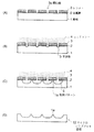
基板1として、酸化珪素が49%、酸化アルミニウムが10%、酸化ホウ素が15%、酸化バリウムが25%の組成比を有する、厚さ0.7mmの無アルカリガラス基板を用意する。この基板1を洗浄した後に、スパッタ法を用いて厚さ100nmのクロム層からなる金属膜2を基板1上に成膜する。次に、スピンコート法を用いて厚さ1000nmのレジスト3を金属膜2上に形成する。このレジスト3には、ポジ型レジストを使用した。上記レジスト3にステッパ露光機を用いて露光して現像することにより、直径3μmの円形の開口部3aを30μmピッチで複数個形成する。
【0109】
次に、金属膜2を硝酸第2セリウムアンモニウムを主成分とする公知のクロムエッチング液を用いてエッチングし、レジスト3の開口部3aの形状と同様の形状に金属膜2を加工して、エッチング用マスクを形成する(図1(A))。ここで、エッチング用マスクとして、レジスト3を剥離せずに残しておく。レジスト3を残すことにより、金属膜形成後からレジスト塗布までの間に金属膜表面に微小な傷が生じた場合に、この傷からのエッチング液の浸透による基板1への影響を低減できるからである。
【0110】
なお、基板1の裏面や端面を、保護テープ、エポキシ系樹脂材料などの保護材(不図示)、上記金属膜2やレジスト3で覆って保護すれば、エッチングによる基板1の厚みや大きさの変化を低減できる。
【0111】
次に、エッチャント4となる10%フッ酸水溶液に基板1を20分間浸して、基板1のエッチングを行う。
【0112】
図1(B)はエッチングの初期段階の状態を示した断面図である。
【0113】
エッチングが始まると、上記開口部3aより基板1の等方性エッチングが進行し、開口部3aを中心とする概半球状の微小な窪みが生じる。エッチングにより、この微小な窪み中の基板表面にエッチャント4に対する不溶物5となるフッ化アルミニウムとフッ化バリウムが主に生成される。この不溶物5は、基板1に均一に含有される酸化アルミニウムおよび酸化バリウムと、エッチャント4に含まれるフッ酸との反応により生成されるものである。
【0114】
上記不溶物5は、エッチングの進行とともに窪み中に蓄積され、窪み内の基板表面を覆うとともに、エッチャント4の循環を阻害する。このため、次第に基板1のエッチングの進行が阻害され、15分程度でエッチングは停止し、それ以降はエッチングが進行しない状態になった。この状態を示した断面図が図1(C)である。
【0115】
これ以降はエッチング時間によらず、窪みの形状は変化しない。本実施形態では、エッチングされた領域が隣接するレンズと重なり合う状態まで進行したところでエッチングが停止し、一つのレンズに注目するとレンズの周囲四箇所に柱状パターン1aが形成された。
【0116】
この後、アセトンを用いてレジスト3を剥離して、上記クロムエッチング液を用いて金属膜2を剥離すると、フッ化アルミニウムを主成分とする不溶物5は上記窪みから洗い流される。さらに、基板1の裏面および端面に上記保護材(不図示)を設けている場合にはこの保護材(不図示)の剥離を行って、直径約40μmの半球状のレンズが30μmピッチで複数形成されたマイクロレンズアレイ基板12が得られる(図1(D))。
【0117】
なお、本実施形態では、上述のように、基板1はエッチャント4と反応してエッチャント4に対する不溶物5を生成する物質となる酸化アルミニウムおよび酸化バリウムをそれぞれ均一に含有する被エッチング体であり、エッチャント4は基板1に含まれる酸化アルミニウムおよび酸化バリウムと反応してエッチャント4に対する不溶物5を生成するエッチング液である。このような基板1とエッチャント4との組み合わせとして、基板1としては、無アルカリガラス、低アルカリガラス、ホウ珪酸ガラス、鉛ガラス、β―石英型透明結晶化ガラスなどがあり、酸化アルミニウム、酸化マグネシウム、酸化カルシウム、酸化カリウム、酸化ストロンチウム、酸化バリウム、酸化リチウム、酸化ナトリウム、酸化セシウム、酸化亜鉛、および酸化鉛のうち少なくとも一つを含有するガラスを用いることができる。また、エッチャント4としては、フッ酸、フッ酸にフッ化アンモニウムを加えたバッファードフッ酸、フッ酸に硝酸などを加えたフッ硝酸エッチング液等のフッ酸系のエッチング液を用いることができる。
【0118】
また、不溶物5として、上記フッ化アルミニウムおよびフッ化バリウムの他に、酸化マグネシウム、酸化カルシウム、酸化ストロンチウム、酸化リチウム、酸化ナトリウム、酸化セシウム、酸化亜鉛、酸化鉛がそれぞれフッ酸と反応して、フッ化マグネシウム、フッ化カルシウム、フッ化ストロンチウム、フッ化リチウム、フッ化ナトリウム、フッ化セシウム、フッ化亜鉛、フッ化鉛が生成される。
【0119】
さらに、基板1とエッチャント4とは、エッチャント4が基板1に含まれる一部の物質を溶解しないような組み合わせであってもよい。このような組み合わせとして、基板1としてはオキシハライドガラスを用いることができ、エッチャント4としては上記フッ酸系エッチング液を用いることができる。フッ酸系エッチング液に溶解しない物質としては、フッ化カルシウム、フッ化ナトリウム、フッ化バリウム、フッ化アルミニウム、フッ化ストロンチウム、およびフッ化マグネシウムなどがある。このような、エッチャント4に溶解しない物質が基板1に少なくとも一つ含まれていることにより、基板1のエッチングが進むにつれて、エッチャント4に溶解しない物質が基板1の表面を覆い、上記不溶物5と同様な作用および効果を生じさせる。
【0120】
本発明を実施する際、エッチング用マスクの開口部直径は、次のような理由で、重要な要素となる。開口部直径が小さすぎると、エッチングの進行が十分に進まない状態で、不溶物5の影響によりエッチャント4の循環が阻害されるために、エッチングが停止してしまう。開口部直径が大きすぎると、エッチャント4の循環が阻害されにくくなるため、エッチングが不溶物5により停止する前に隣接するマイクロレンズとエッチング領域が重なり、エッチング用マスクの剥離が発生してエッチングが停止しなくなる。また、開口部のピッチが小さすぎる場合にも、エッチングが停止する前に、隣接するマイクロレンズとエッチング領域が重なり、エッチング用マスクの剥離が発生することとなる。
【0121】
上述のことから、エッチング用マスクの開口部直径および開口部ピッチの大きさを変えて数多くの実験を実施したので、その結果について説明する。
【0122】
表1は、上記作製条件において、円形開口部の直径と開口部のピッチとを変えてエッチングを行った結果をまとめたものである。なお、表1に表わされる○印はエッチングの進行が所定の状態で停止したことを示す。また、×印はエッチングの進行が停止しなかったことを示し、※印はエッチングの進行が十分に進まない状態でエッチングが停止したことを示す。
【0123】
【表1】

表1に示す結果から、開口部直径の大きさが開口部のピッチの1/10以上1/3以下の範囲において、本発明の目的が達成されることが明らかである。
【0125】
また、表1に示す○印で得られたマイクロレンズの直径は、隣接するレンズ同士が接する状態の大きさから、隣接するレンズのエッチング領域が重なるがエッチング用マスクの剥離が生じない状態までの大きさであり、表1に示した開口部ピッチの1.0〜1.4倍の大きさであった。この結果から、表1を用いることにより、作製するマイクロレンズの直径寸法から開口部のピッチと開口部の直径を決めることができる。例えば、レンズの直径が30〜40μmのマイクロレンズアレイを作製するには、表1から、開口部のピッチを30μmにした場合、開口部の直径を3〜10μmにすればよいことがわかる。
【0126】
また、開口部の形状が円形の替わりに正方形である場合についても、数多くの実験を実施したので、その結果について説明する。
【0127】
表2は、正方形の一辺の長さである開口部辺長と開口部のピッチとを変えてエッチング後の状況をまとめたものである。なお、表2に示される各印の意味については上記表1と同様である。
【0128】
【表2】
表2に示す結果から、開口部辺長が開口部のピッチの1/10以上1/3以下の範囲において、本発明の目的が達成されることが明らかである。このように、本発明は開口部の形状には大きく依存しないことが判明した。そのため、上記エッチング用マスクの開口部3aの形状は、本実施形態では円形としているが、方形、楕円形、その他の形状でもよい。
【0130】
次に、エッチャント濃度に対する依存性について検討するためにフッ酸水溶液の濃度を変えてエッチングを行ったので、その結果について説明する。
【0131】
表3は、開口部のピッチ30μm、開口部直径3μmのエッチング用マスクを設けた場合について、フッ酸水溶液の濃度を5%、10%、20%、30%とした場合のエッチング時間をまとめたものである。なお、このエッチング時間は、エッチングの進行が不溶物5の影響により自動的に停止するまでの時間を意味する。
【0132】
【表3】
表3に示す結果から、フッ酸濃度が高いほどエッチングの進行が停止するまでの時間が短くなっている。また、それぞれのエッチング条件により得られたレンズ形状について観察を行ったところ、どの条件でもほぼ同様の形状が得られていることが判明した。これは、本発明がエッチャント4の濃度には大きく依存しないことを示唆している。すなわち、エッチャント濃度が多少変化し、これによりエッチングが停止するまでの時間が変動しても、エッチングが不溶物5により自動的に停止するため、オーバーエッチングが発生することはない。また、予め所定のエッチング時間より長めの時間を設定しておくことで、エッチング不足を防止することも可能である。
【0134】
なお、基板1に含有される、エッチャント4に溶解しない物質である不純物の濃度に関しては、エッチャント濃度が同じでも、不純物濃度が高い場合にはエッチングの進行の停止が早くなり、不純物濃度が低い場合には不溶物の生成が不十分となるためエッチングの進行の停止が遅くなる傾向がある。そのため、形成されるレンズの直径は、基板1の不純物濃度による影響を受けることとなる。このことから、基板1に含有される酸化アルミニウム等の不純物の濃度は基板内および基板間で一定である方がよい。
【0135】
次に、エッチャント4の温度に対する依存性について検討するためにフッ酸水溶液の温度を変えてエッチングを行ったので、その結果について説明する。
【0136】
表4は、エッチャント中のフッ酸濃度を10%に固定し、エッチャント温度を変えてエッチング時間を調べた結果をまとめたものである。なお、このエッチング時間は、上記表3と同様にエッチングの進行が停止するまでの時間を意味する。
【0137】
【表4】
表4に示す結果から、エッチャントの温度が高いほどエッチングの進行が停止するまでの時間が短くなっている。また、それぞれのエッチング条件により得られたレンズ形状について観察を行ったところ、どの条件でも同様の形状が得られていることが判明した。これは、本発明がエッチャントの温度にも大きく依存せず、厳密な温度管理が不要であることを意味する。また、濃度を変えた場合と同様に、厳密な時間管理が不要で、エッチング不足およびオーバーエッチングを防止することも可能である。
【0139】
次に、エッチング用マスクについての検討結果を以下に説明する。
【0140】
エッチング用マスクの材質については、エッチャント4により変質が発生しにくいこと、および基板1との密着性が高いことが好ましい。密着性が低い場合には、基板1とエッチング用マスクとの界面からエッチングが進行し、エッチングムラの一因となるためである。本実施形態のようなクロム層などの金属膜2は、フッ酸系エッチング液に対して変質しにくく、基板1との密着性がよい。
【0141】
次に、エッチング用マスクの金属膜2に用いたクロム層の厚みについて検討した結果を以下に説明する。
【0142】
表5はクロム層の厚みを10nmから500nmの間で変化させた場合のエッチング結果をまとめたものである。
【0143】
【表5】
表5に示すように、クロム層の厚みが10nm以下の場合と500nm以上の場合にクロム層がマスクとして使用できない状態になり、その理由は以下の通りである。
【0145】
クロム層の厚みが10nm以下の場合にはクロム層にピンホールが発生し、エッチング用マスクとしての機能が十分に発揮できないため、エッチング用マスクの剥離が発生して、良好なエッチング状態を得ることができなかった。また、クロム層の厚みが500nm以上の場合には多数のクラックが発生するとともに、エッチングの進行に伴ってクロム層の応力に起因すると考えられる剥離が発生して、良好なエッチング状態を得ることができなかった。このため、本発明におけるクロム層の厚みは20nmから300nmの範囲に設定されることが好ましい。また、クロムのかわりにシリコン、チタン、銀、白金、金などを使用することができるが、クロムの場合と同様な現象が発生するため、上記の厚みの範囲で使用することが好ましい。
【0146】
次に、エッチング用マスクのレジスト3の厚みについて検討した結果を以下に説明する。
【0147】
表6はレジスト3の厚みを100nmから6000nmの間で変化させた場合のエッチング結果をまとめたものである。
【0148】
【表6】
表6に示すように、レジスト3の厚みが100nm以下の場合と6000nm以上の場合にレジスト3がマスクとして使用できない状態になり、その理由は以下の通りである。
【0150】
レジスト3の厚みが100nm以下の場合にはエッチングの進行とともにエッチング用マスクの剥離が発生して、良好なエッチング状態を得ることができなかった。また、レジスト3の厚みが6000nm以上の場合にも、エッチングの進行とともにエッチング用マスクの剥離が発生して、良好なエッチング状態を得ることができなかった。このため、本発明におけるレジスト3の厚みは200nmから4000nmの範囲に設定されることが好ましい。
【0151】
なお、本実施形態は、マイクロレンズアレイのみならず、単体のマイクロレンズの形成にも同様に適用することが可能である。
【0152】
本実施形態では、上述したように、不溶物5が生成されることで基板1のエッチングが自動的に停止する効果により、エッチングが停止した後に基板1をエッチャント4に浸していてもエッチングが進行しない。そのため、エッチング停止後に基板1をエッチャント4から取り出す時間のマージンを大きく確保できる。
【0153】
また、複数枚の基板1を一度に加工する際にも、上記不溶物5の生成が基板間で均一なため、基板間で均一な加工が可能になる。また、一枚の基板1を複数回のエッチング処理で加工する場合にも、上記不溶物5の生成がエッチング処理間で均一なため、エッチング処理間で均一な加工が可能となる。そのため、基板1が大型化しエッチャント濃度やエッチング時間に面内分布が発生しても、基板面内のみならず基板間で均一なレンズパターンを作製することができ、基板面内および基板間における凹部形状の均一性により歩留りが向上し、ウェットエッチングにより低コスト化が可能となる。
【0154】
また、発生した不溶物5がエッチング用マスクの支えの役割を果たすため、金属膜2およびレジスト3から構成されるエッチング用マスクの剥離を防止することができ、より均一性の高い加工が可能になる。さらに、無アルカリガラス、低アルカリガラス、ホウ珪酸ガラス、鉛ガラスなどの液晶表示用ガラスは石英ガラス基板やシリコンウェハ基板と比較して安価であり、本実施形態では、これらの液晶表示素子用ガラスを使用することができるため、低コスト化も実現可能である。
【0155】
なお、本実施形態によるマイクロレンズアレイ基板12を液晶表示素子に応用する場合について説明する。
【0156】
図2は液晶表示素子の外観を模式的に示す斜視図である。
【0157】
図に示すように、液晶表示素子は、マイクロレンズアレイ基板12上に設けられた調整用ガラス板51と公知の方法により作製されたTFT基板50との間に液晶層52が挟まれる構成である。
【0158】
上記構成の液晶表示素子では、図の下側から照射された光がマイクロレンズアレイ基板12に設けられたマイクロレンズによりTFT基板50の透過部で集光するように構成されているため、光を透過するように液晶分子が配列した部分の輝度が高くなる。また、本実施形態のマイクロレンズアレイ基板12を用いることにより、表示面内の輝度が均一になる。
【0159】
上記液晶表示素子の作製方法について説明する。
【0160】
図3乃至図5は液晶表示素子の作製方法を製造工程順に示した断面図である。
【0161】
図3(A)に示すように、無アルカリガラスの基板201上に金属膜202およびレジスト203を順に形成し、公知のリソグラフィ工程およびエッチング工程によりレジスト203と金属膜202に開口部203aを形成する。開口部203aを形成する際、以下に説明する露光位置調整マーカ203bを形成する。なお、図1では、露光位置調整マーカ203bを図に示すことを省略した。
【0162】
露光位置調整マーカ203bは基板201上の所定の場所に必要な数だけ設けられている。露光位置調整マーカ203bは、ステッパ露光機による、上記開口部203aを形成するための第1の露光とそれ以降に行う露光の際、ステッパ露光機用マスクであるレチクルやTFT基板等との相対的な位置決めのために用いられる位置合わせ手段であり、一般的にその精度は1μm以下である。なお、工程数は増えるが露光位置調整マーカ203bを形成した後に、開口部203aを形成してもよい。
【0163】
続いて、図3(B)に示すように、基板201をエッチャントに浸す前に、露光位置調整マーカ203bをエッチャントから保護するための保護材253を形成する。この保護材253はエッチャントに対する耐性を有するものであればよく、保護材253として、特に保護テープやエポキシ系樹脂材料等を好適に用いることが可能である。
【0164】
そして、図3(C)に示すように、基板201をエッチャントに浸して、基板201のエッチングを行う。このとき、保護材253が露光位置調整マーカ203bの形状変化や剥離を防止する。また、レンズとなる凹部の周囲に柱状パターン201aを有するため、レジスト203と金属膜202の剥離を防止する。
【0165】
その後、図3(D)に示すように、保護材253を剥離し、レジスト203と、露光位置調整マーカ203b以外の金属膜202を剥離する。ここでは、保護材253を剥離したが、この後のステッパ露光機によるステッパ露光の際、問題とならなければ特に剥離する必要はない。
【0166】
続いて、図3(E)に示すように、マイクロレンズアレイ基板212の凹部形成面に高屈折率接着剤254を塗布して透明な調整用ガラス板251を貼合する。このとき、マイクロレンズアレイのレンズの焦点距離を調整して、レンズとしての効果が最大となるように調整用ガラス板251の厚さを調整する。マイクロレンズアレイ基板212に調整用ガラス板251を貼り合わせた後に調整用ガラス251を薄くして厚さ調整してもよいが、予め厚さ調整した調整用ガラス板251をマイクロレンズアレイ基板212に貼合してもよい。貼合後に薄くする場合には、エッチング法や機械研磨法を好適に用いることが可能である。このように透明基板として調整用ガラス板251を凹部形成面側に貼合することで、凹部に埋め込まれた高屈折率接着剤254の形状を維持し、凹部で屈折した光が調整用ラス板251を透過可能となる。
【0167】
その後、調整用ガラス板251上にクロムやアルミニウム等の薄膜を成膜し、その上にレジストを塗布する。そして、重ね合わせ位置調整マーカ255および画素遮光部256のパターンを形成するためのレチクルに備えたマーカと、露光位置調整マーカ203bを使用して、レチクルとマイクロレンズアレイ基板212を位置決めして、ステッパ露光および現像を行う。続いて、エッチングによりレジストマスクの形状に合わせたパターンを形成するパターニングにより、重ね合わせ位置調整マーカ255と画素遮光部256を形成する(図3(F))。
【0168】
このように、ステッパ露光時のレチクルとマイクロレンズアレイ基板212の位置決めのために露光位置調整マーカ203bを使用している。そのため、重ね合わせ位置調整マーカ255と画素遮光部256をより正確に所望の位置に配置できる。この重ね合わせ位置調整マーカ255は、液晶表示素子を作製する際に使用するTFT基板と高精度に重ね合わせるために用いられる。TFT基板との重ね合わせを高精度に行い得るため、画素遮光部256等の重ね合わせマージンをより小さくでき、開口率がより高くなり、より明るい表示が可能な液晶表示素子を作製可能となる。なお、画素遮光部256はTFT等に光が当たるのを防止するための遮光手段である。
【0169】
その後、公知の方法により、調整用ガラス板251上に、図に示さない透明電極および配向膜等を形成する。
【0170】
なお、上記高屈折率接着剤を用いて貼合する代わりに、形成された凹部に高屈折率材料を埋め込み、調整用ガラス板251とほぼ同一の屈折率の接着剤を用いてマイクロレンズアレイ基板212と調整用ガラス板251を接着してもよい。また、上記高屈折率接着剤および高屈折率材料の屈折率を調整することで、マイクロレンズアレイのレンズの焦点距離を調整することが可能である。
【0171】
次に、TFT基板とマイクロレンズアレイ基板を重ね合わせる方法について説明する。重ね合わせ方法は大きく分けて二つある。一つめの方法は、TFT基板とマイクロレンズアレイ基板を重ね合わせた後に個片に切断する方法であり、二つめの方法は、TFT基板とマイクロレンズアレイ基板を個片に切断してから重ね合わせる方法である。
【0172】
はじめに、一つめの重ね合わせ方法について説明する。
【0173】
図4は一つめの重ね合わせ方法を示す断面模式図である。
【0174】
図3(F)に示したマイクロレンズアレイ基板212を用意する(図4(A))。続いて、図4(B)に示すように、公知の方法により作製されたTFT基板250とマイクロレンズアレイ基板212を、重ね合わせ位置調整マーカ255とTFT基板側重ね合わせ位置調整マーカ257を使用して位置を合わせ、シール剤258で貼り合わせる。このとき、TFT基板250とマイクロレンズアレイ基板212には、液晶を入れるための隙間を設けている。なお、露光位置調整マーカ203bを形成するときに、重ね合わせ位置調整マーカをマイクロレンズアレイ基板212の表面に形成し、この重ね合わせ位置調整マーカをTFT基板250との重ね合わせ時に使用してもよい。
【0175】
続いて、図4(C)に示すように、切断箇所に高圧の水をかける切断方法で、貼り合わせたTFT基板250とマイクロレンズアレイ基板212を個片に分離し、貼り合わせた2枚の板の間に液晶を封入して液晶層252を形成して液晶表示素子260を得る。この切断方法によれば、マイクロレンズアレイ基板212と調整用ガラス板251が高屈折率接着剤254で貼合されているような構造でも、効率よく切断できる。なお、液晶層252を、TFT基板250とマイクロレンズ基板212を貼り合わせる際に封入してもよい。
【0176】
次に、二つめの重ね合わせ方法について説明する。
【0177】
図5は二つめの重ね合わせ方法を示す断面模式図である。
【0178】
図5(A)に示すように、マイクロレンズアレイ基板212を個片に切断する。個片にしたマイクロレンズアレイ基板212aにも、重ね合わせ位置調整マーカ255が形成されている。続いて、図5(B)に示すように、個片にしたTFT基板250aと個片にしたマイクロレンズアレイ基板212aを、重ね合わせ位置調整マーカ255とTFT基板側重ね合わせ位置調整マーカ257を使用して位置を合わせ、シール剤258で貼り合わせる。貼り合わせた2枚の板の間に液晶を封入して液晶層252を形成し、液晶表示素子260を得る。
【0179】
なお、図4および図5では、マイクロレンズアレイ基板212の凹部形成面側に調整用ガラス基板251を貼り合わせ、調整用ガラス基板251とTFT基板250の間に液晶層252を形成したが、以下に説明するように、マイクロレンズアレイ基板212とTFT基板250の間に液晶層252を形成するようにしてもよい。
【0180】
図6は液晶表示素子の別の構成例を示す断面図である。
【0181】
図5に示した個片にしたマイクロレンズアレイ基板212aの上下方向を逆にし、図6に示すように、個片にしたマイクロレンズアレイ基板212aのレンズが図の上向きで凸形状になるようにしている。図6に示す構造を形成する場合には、レンズの効果が最大となるように個片にしたマイクロレンズアレイ基板212aの厚さを調整している。マイクロレンズアレイ基板212の凹部形成面に調整用ガラス251を貼り合わせた後にマイクロレンズアレイ基板212の厚さを調整してもよいが、予めマイクロレンズアレイ基板212の厚さを調整してから調整用ガラス板251を貼合してもよい。貼合後に薄くする場合には、エッチング法や機械研磨法を好適に用いることが可能である。
【0182】
液晶表示素子のTFT基板とマイクロレンズアレイ基板は、単位長さあたりの熱膨張係数である線熱膨張係数が比較的近いことが好ましい。これら2枚の基板に線熱膨張係数が大きく異なるものを使用すると、ヒートサイクルでの基板剥離等による信頼性低下と、熱膨張による位置目合わせずれが問題になる。TFT基板には、無アルカリガラスまたは石英基板が多く使用される。このとき、TFT基板の基板の種類に応じて、マイクロレンズアレイ基板に無アルカリガラスやβ―石英型透明結晶化ガラス等を使用することで、TFT基板とマイクロレンズアレイ基板の線熱膨張係数が等しくなり、上記問題の発生が抑制され、信頼性がより向上する。
【0183】
次に、作製された液晶表示素子を液晶プロジェクタの液晶ライトバルブとして応用する場合について説明する。
【0184】
図7は液晶プロジェクタの一構成例を示す模式図である。
【0185】
図に示すように、液晶プロジェクタは、光源130と、光源130からの光の偏光方向を揃えるとともに光強度を均一にする偏光変換インテグレータ132と、光源130からの白色光をダイクロイックミラー133、134により赤色、緑色および青色の3色の光束に分離する色分離光学系と、分離された光束の進行方向を変えるための全反射ミラー135〜137と、上記3色の光束が色別に照射される3枚の液晶表示素子138〜140と、これら3枚の液晶表示素子138〜140によって表示される画像を合成するためのクロスダイクロイックプリズム141からなる色合成光学系と、合成された表示画像をスクリーン上に拡大投射するための投射レンズ142とを備える構成である。
【0186】
液晶表示素子138〜140は、薄膜トランジスタ(TFT)を画素毎に配列して液晶を駆動させるアクティブマトリクス型である。また、各液晶表示素子138〜140のクロスダイクロイックプリズム141側の面に、偏光方向が偏光変換インテグレータ132の偏光方向と直交する偏光板(不図示)が設けられている。
【0187】
次に、上記構成の液晶プロジェクタの動作について説明する。
【0188】
液晶プロジェクタは、図に示すように、光源130から出射された光をリフレクタ131で集光した後、その光束からダイクロイックミラー133で赤色の光束を分離し、ダイクロイックミラー134で緑色の光束を分離して、赤色、緑色および青色の3色の光束に分離する。赤色の光束は、全反射ミラー135で反射した後、赤色用液晶表示素子138を照明する。また、緑色の光束は緑色用液晶表示素子139を照明し、青色の光束は全反射ミラー136、137で順次反射した後、青色用液晶表示素子140を照明する。赤色、緑色、および青色の液晶表示素子138〜140に表示される各画像は、クロスダイクロイックプリズム141によって合成された後、投射レンズ142によりスクリーン(不図示)に拡大投影される。
【0189】
上記構成による液晶プロジェクタは、マイクロレンズが入射される光を画素の開口部に集光するため、輝度が向上してスクリーン上の投影像がより明るくなり、本発明のマイクロレンズアレイ基板12を用いることにより、投影像の全体の明るさが均一になる。
【0190】
次に、上記液晶表示素子を液晶表示装置に応用する場合について説明する。
【0191】
図8は半透過型の液晶表示装置の外観を模式的に示す斜視図である。
【0192】
図に示すように、液晶表示装置は、上記液晶表示素子151と、偏光板152、153と、光源となるバックライトユニット154と、画素毎に設けられたTFTに信号を送るための信号供給回路155と、バックライトユニット154および信号供給回路155に電源を供給する電源供給部156とを備える構成である。
【0193】
バックライトユニット154に赤色、緑色および青色からなる3原色のランプを設けて、この3原色ランプの点灯を高速で切り換える制御を行うことにより液晶表示装置の画面をカラー表示にできるが、バックライトユニット154に3原色ランプを設ける代わりに液晶表示素子151にカラーフィルターを設けてもよい。
【0194】
上記構成による液晶表示装置は、マイクロレンズアレイがバックライトの光利用率を高めるため表示がより明るくなり、本発明のマイクロレンズアレイ基板12を用いることにより、表示画面内における輝度が均一になる。
【0195】
本実施形態による液晶表示素子を、例えば、特開2000−298267号公報に示される半透過型の液晶表示装置に用いることができる。
【0196】
なお、本実施形態により作製された液晶表示素子を、上記半透過型の液晶表示装置に限らず、半透過型より遮光率の大きい微透過型、および半透過型より遮光率の小さい微反射型の液晶表示装置にも適用できる。
【0197】
(第2の実施形態)
第2の実施形態では、上記第1の実施形態により作製されたマイクロレンズアレイ基板12を、2P成型法によるマイクロレンズアレイ作製のための母型に用いたものである。
【0198】
図9は本発明の第2実施形態を製造工程順に示した断面図である。
【0199】
まず、図9(A)に示すように、母型6の凹部形成面に離型剤7と、樹脂8として紫外線硬化樹脂とを順に塗布した後、樹脂8を塗布した面を下側に向ける。
【0200】
次に、基板30として無アルカリガラスを用いて基板30の面と樹脂8の面とを合わせて、母型6を基板30側に押し付ける(図9(B))。樹脂8に紫外線を照射して硬化させた後、母型6を剥離することで、凸型に成型された樹脂8を基板30上に形成し、樹脂8と基板30とからなるマイクロレンズアレイ32が得られる(図9(C))。
【0201】
なお、図9(C)に示した工程の後、樹脂8の上から全面に異方性エッチングを行い、樹脂8の凸型形状を基板30に転写してもよい。
【0202】
また、上記樹脂8は、光照射により硬化する光硬化樹脂、加熱により硬化する熱硬化樹脂、または2液性接着剤であっても好適である。上記母型6の材料としては、基板30と同種のものか、基板30と熱膨張係数の近いものを用いるとよい。
【0203】
本実施形態では、上記第1の実施形態のマイクロレンズアレイ基板12には大面積に均一な凹部形状が形成されているため、マイクロレンズアレイ基板12を母型6に用いることで、大型の母型を高い歩留まりで安価に作製することが可能となる。
【0204】
また、母型6と基板30に同種の材料、または熱膨張係数の近い材料を用いることにより、母型6の材料として金属や石英ガラス基板など、基板30と異なる材料を用いる場合と比較して、熱膨張係数の違いに起因する誤差を小さくでき、厳密な温度管理が不要となる。また、熱硬化樹脂を用いた際の、加熱工程で生じる誤差を小さくすることができる。
【0205】
さらに、母型6および基板30の材料として、安価な無アルカリガラスなどを用いることができるため、低コスト化が可能となる。また、大型の母型6を使用してマイクロレンズアレイ32を成型できるため、小型の母型を用いて多数回、高精度で型押しする必要はなく、コスト面で有利となる。
【0206】
なお、本実施形態により作製されたマイクロレンズアレイ32を液晶プロジェクタのライトバルブ用マイクロレンズアレイとして使用する場合には、次のような工程を追加する。
【0207】
まず、マイクロレンズアレイ32の凸型成型面に樹脂8または基板30に比べて低屈折率な接着剤を塗布してガラスを貼合する。次に、マイクロレンズアレイ32の凸部に形成されたレンズの焦点が公知の方法で作製されたTFT基板の透過部に合うように、ガラスの厚みを調整した後、上記TFT基板をマイクロレンズアレイ12に貼り合わせて、ライトバルブ用マイクロレンズアレイを得る。
【0208】
この後、ライトバルブ用マイクロレンズアレイに配線となる透明電極や位置合わせのためのマーカなどの形成を行い、公知のパネル作製工程を実施することで、液晶プロジェクタ用のマイクロレンズアレイ付ライトバルブを得る。
【0209】
また、本実施形態により作製されたマイクロレンズアレイ32を、マイクロレンズアレイ付液晶表示素子に応用するためには、次のような工程を実施すればよい。なお、マイクロレンズアレイ付液晶表示素子の応用例としては、半透過型、微透過型、または微反射型の液晶表示素子である。
【0210】
まず、適当な厚みの基板を用いて公知の方法により作製した液晶表示素子の光入射側基板の表面に樹脂8を塗布して、この樹脂8に上記母型6を用いて型押しを行った後、樹脂8を硬化させてマイクロレンズアレイ32を得る。次に、マイクロレンズアレイ32のレンズを透過するバックライト光がTFT基板の画素電極の透過部に集光するように位置合わせを行って、光入射側基板をTFT基板に組み付けることで、マイクロレンズアレイ付液晶表示素子を得る。これにより、レンズパターンの均一なマイクロレンズアレイ付液晶表示素子をより低コストで作製できる。
【0211】
(第3の実施形態)
第3の実施形態は、本発明を等方性エッチング法による光導波路の作製に適用する形態である。
【0212】
図10は本発明の第3の実施形態を製造工程順に示した断面図である。
【0213】
図10(A)に示すように、基板1として、第1の実施形態と同様に、酸化アルミニウム等を均一に含有する無アルカリガラスを用いて、この基板1上に金属膜2およびレジスト3からなるエッチング用マスクを形成する。
【0214】
なお、光導波路のパターンに倣った四角形の開口部3bをエッチング用マスクに形成するが、開口部3bの対向する二辺の幅については、第1の実施形態で示した表1のような、上記開口部3bの幅と形成される光導波路の幅との関係を示す表を予め作成し、作成した表に基づいて形成される光導波路の幅から決定する。
【0215】
次に、エッチャント4としてフッ酸系エッチング液を用いて基板1のエッチングを行う。図10(B)はエッチングの初期段階の状態を示した断面図である。
【0216】
エッチングが始まると、上記開口部3bから基板1の等方性エッチングが進行し、微小な溝部が形成される。この微小な溝部中の基板表面に、エッチングにより生じた、エッチャントに対する不溶物5であるフッ化アルミニウム等が蓄積し、基板1のエッチングの進行を阻害し、最終的にはエッチングが停止して光導波路パターンが形成される(図10(C))。
【0217】
金属膜2およびレジスト3とともに不溶物5を除去した後、基板1に比べて屈折率の高い高屈折率材料を、形成された溝部に埋め込み、光導波路13を形成する(図10(D))。
【0218】
本実施形態では、基板1にエッチャント4に対する不溶物5を生成する物質として酸化アルミニウム等が含まれ、エッチングによりエッチャント4に対する不溶物5が生成されるため、ある程度エッチングが進行した状態でエッチングが自動的に停止し、エッチングストッパ層などを設けることなく、大面積の基板でも均一な光導波路のパターンを安価に作製することができる。また、各エッチング処理におけるエッチング量のばらつきがなく、エッチング処理間における凹部形状が均一な光導波路用パターンを形成できる。
【0219】
また、第1の実施形態で述べたように、基板1がオキシハライドガラスであれば、フッ酸系エッチング液に溶解しない物質としてフッ化カルシウム等が含有されるため、フッ化カルシウム等が上記不溶物5と同様な作用および効果を生じさせる。
【0220】
なお、金属膜2およびレジスト3とともに不溶物5を除去した後、作製された光導波路状の窪みパターンを母型にして、2P成型法を用いて別の基板上に高屈折率材料を成型した光導波路を形成することにより、ストリップ導波路やリブ導波路を得ることも可能である。この場合にも、大型の母型を高い歩留まりで安価に作製することが可能であること、熱膨張係数の違いに起因する誤差を小さくでき厳密な温度管理が不要となること、熱硬化樹脂を用いた際の加熱工程における誤差を小さくできること、母型の材料として安価な無アルカリガラスなどを用いることができるため低コスト化が可能であること、などの効果を得ることができる。
【0221】
(第4の実施形態)
第4の実施形態は、本発明を等方性エッチング法による埋め込み配線の作製に適用する形態である。
【0222】
図11は本発明の第4の実施形態を製造工程順に示した断面図である。
【0223】
図11(A)に示すように、基板1として、第1の実施形態と同様に、酸化アルミニウム等を均一に含有する無アルカリガラスを用いて、この基板1上に金属膜2およびレジスト3からなるエッチング用マスクを形成する。
【0224】
なお、埋め込み配線のパターンに倣った四角形の開口部3cをエッチング用マスクに形成するが、開口部3cの対向する二辺の幅については、第1の実施形態で示した表1のような、上記開口部3cの幅と形成される埋め込み配線の幅との関係を示す表を予め作成し、作成した表に基づいて形成される埋め込み配線の幅から決定する。
【0225】
次に、エッチャント4としてフッ酸系エッチング液を用いて基板1のエッチングを行う。図11(B)はエッチングの初期段階の状態を示した断面図である。
【0226】
エッチングが始まると、上記開口部3cより基板1の等方性エッチングが進行し、微小な溝部が形成される。この微小な溝部中の基板表面に、エッチングにより生じた、エッチャントに対する不溶物5であるフッ化アルミニウム等が蓄積し、基板1のエッチングの進行を阻害し、最終的にはエッチングが停止して配線パターンが形成される(図11(C))。
【0227】
金属膜2およびレジスト3とともに不溶物5を除去した後、スパッタ法などの公知の方法を用いて、配線用金属層9を成膜する(図11(D))。次に、化学的または機械的な研磨法を用いて、形成された溝部中以外の配線用金属層9を除去して、埋め込み配線9aを形成する(図11(E))。
【0228】
本実施形態では、基板1にエッチャント4に対する不溶物5を生成する物質として酸化アルミニウム等が含まれ、エッチングによりエッチャント4に対する不溶物5が生成されるため、ある程度エッチングが進行した状態でエッチングが自動的に停止し、大面積の基板でも均一な埋め込み配線用のパターンを安価に作製することができる。また、各エッチング処理におけるエッチング量のばらつきがなく、エッチング処理間における凹部形状が均一な埋め込み配線用パターンを形成できる。
【0229】
また、第1の実施形態で述べたように、基板1がオキシハライドガラスであれば、フッ酸系エッチング液に溶解しない物質としてフッ化カルシウム等が含有されるため、フッ化カルシウム等が上記不溶物5と同様な作用および効果を生じさせる。
【0230】
(第5の実施形態)
第5の実施形態は、本発明を等方性エッチング法による回折格子の作製に適用する形態である。
【0231】
図12は本発明の第5の実施形態を製造工程順に示した断面図である。
【0232】
図12(A)に示すように、酸化アルミニウム等を均一に含有する無アルカリガラスの基板1上にスピンコートなどの公知の手法を用いて、レジスト3を塗布し、乾燥させる。なお、レジスト3としては、次工程の露光で使用する光の波長に対応し、かつ回折格子を形成できるだけの解像度を有するものを使用する。一例として、エキシマレーザ用フォトレジストを好適に使用することができる。
【0233】
この後、エキシマレーザ光などを使用してレジスト3に干渉露光を行い、レジストの現像工程を経て、微細な開口部3dからなる回折格子パターンを有するエッチング用マスクを形成する(図12(B))。
【0234】
なお、回折格子のパターンに倣った四角形の開口部3dをエッチング用マスクに形成するが、開口部3dの対向する二辺の幅および開口部3dの間隔については、第1の実施形態で示した表1のような、上記開口部3dの幅および間隔と形成される回折格子の凹部の幅との関係を示す表を予め作成し、作成した表に基づいて形成される回折格子の凹部の幅から決定する。
【0235】
次に、エッチャント4としてフッ酸系エッチング液を用いて基板1のエッチングを行う。図12(C)はエッチングの初期段階の状態を示した断面図である。
【0236】
エッチングが始まると、開口部3d部分より基板1の等方性エッチングが進行し、微小な溝部が形成される。この微小な溝部中の基板1の表面に、エッチングにより生じた、エッチャント4に対する不溶物5であるフッ化アルミニウム等が蓄積し、基板1のエッチングの進行を阻害し、最終的にはエッチングが停止する。
【0237】
この後、レジスト3の剥離を行って不溶物5を洗い流すと、図12(D)に示すように、複数の溝部が設けられた回折格子34が形成される。
【0238】
本実施形態では、基板1にエッチャント4に対する不溶物5を生成する物質として酸化アルミニウム等が含まれ、エッチングによりエッチャント4に対する不溶物5が生成されるため、ある程度エッチングが進行した状態でエッチングが自動的に停止し、大面積の基板でも均一な回折格子のパターンを安価に作製することができる。また、各エッチング処理におけるエッチング量のばらつきがなく、エッチング処理間におけるパターン形状が均一な回折格子を形成できる。
【0239】
なお、基板1は、第1の実施形態と同様に、上記無アルカリガラスの他に、低アルカリガラス、ホウ珪酸ガラス、鉛ガラスでもよい。基板1がオキシハライドガラスであれば、フッ酸系エッチング液に溶解しない物質としてフッ化カルシウム等が含有されるため、フッ化カルシウム等が上記不溶物5と同様な作用および効果を生じさせる。
【0240】
また、このようにして作製された回折格子34は、大面積・安価な光学素子として使用することもできるが、例えば、有機エレクトロルミネッセンス素子の基板として使用することで、光取り出し効率を向上することもできる。この場合には、安価な無アルカリガラス基板を使用して、安価な手法で大面積の回折格子34を作製できる利点を最大限に活用することができる。
【0241】
(第6の実施形態)
第6の実施形態は、本発明を等方性エッチング法による液晶配向膜の作製に適用する形態である。
【0242】
図13は本発明の第6の実施形態を製造工程順に示した断面図である。
【0243】
図13(A)に示すように、基板1上に透明電極10を形成し、透明電極10の上に液晶分子の配列方向を決めるための配向膜11を形成する。なお、この配向膜11は、酸化アルミニウム等を均一に含有させた無機材料の膜である。
【0244】
次に、図13(B)に示すように、第5の実施形態と同様な方法を用いてエッチング用マスクを形成するが、四角形の開口部3eの長手方向を注入する液晶分子の配列方向にほぼ一致させておく。エッチング用マスクの材質としては、レジスト3などを好適に用いることができる。
【0245】
なお、形成される液晶配向膜のパターンに倣った四角形の開口部3eをエッチング用マスクに形成するが、開口部3eの対向する二辺の幅および開口部3eの間隔については、第1の実施形態で示した表1のような、上記開口部3eの幅および間隔と形成される液晶配向膜の凹部の幅との関係を示す表を予め作成し、作成した表に基づいて形成される液晶配向膜の凹部の幅から決定する。
【0246】
この後、エッチャント4としてフッ酸系エッチング液を用いて配向膜11のエッチングを行う。図13(C)はエッチングの初期段階の状態を示した断面図である。
【0247】
エッチングが始まると、配向膜11の等方性エッチングが進行し、微小な溝部が形成される。この微小な溝部中の配向膜表面に、エッチングにより生じた、エッチャント4に対する不溶物5であるフッ化アルミニウム等が蓄積し、配向膜11のエッチングの進行を阻害し、最終的にはエッチングが停止する。
【0248】
次に、レジスト3の剥離を行って不溶物5を洗い流すと、図13(D)に示すように、溝部と直線状突部とが交互に複数設けられた液晶配向膜11aが形成される。
【0249】
本実施形態では、配向膜11にエッチャント4に対する不溶物5を生成する物質として酸化アルミニウム等が含まれ、エッチングによりエッチャント4に対する不溶物5が生成されるため、ある程度エッチングが進行した状態でエッチングが自動的に停止し、大面積の基板上に作製する場合でも均一な凹凸形状を有する液晶配向膜を安価に作製することができる。また、各エッチング処理におけるエッチング量のばらつきがなく、エッチング処理間におけるパターン形状が均一な液晶配向膜を形成できる。
【0250】
また、上記不溶物5を生成させる酸化アルミニウム等を含有させる代わりに、配向膜11にエッチャント4に溶解しない物質として、第1実施形態で述べたフッ化カルシウム等の物質から少なくとも一つ含有させるようにしてもよい。配向膜11にエッチャント4に溶解しない物質を含有させることにより、この物質が上記不溶物5と同様の作用および効果を生じさせる。
【0251】
さらに、上記液晶配向膜11が形成された基板1を2枚用いて、そのうちの1枚にシール材を印刷した後2枚の基板1を貼り合せてパネル化し、パネル内に液晶を注入して液晶表示素子とした。これにより、信頼性、均一性の高い液晶配向膜を、大面積に渡って安価に作製することができる。
【0252】
特に、上記配向膜11として無機材料を用いることにより、液晶が注入される空間を仕切るための隔壁構造と組み合わせて用いた場合に、隔壁作製プロセスによる配向膜のダメージをなくすことができ、配向膜のダメージを受けやすいスメクティック液晶を使用した場合でも均一な配向を得ることができる。
【0253】
(第7の実施形態)
第7の実施形態は、本発明をワイヤーグリッド型の偏光光学素子の作製に適用する形態である。
【0254】
図14は本発明の第7の実施形態を製造工程順に示した断面図である。
【0255】
図14(A)に示すように、基板1上に金属膜20を形成する。なお、金属膜20の材質としては、例えば、TiとAlの合金等が使用可能であり、公知のスパッタ法等を用いて成膜する。
【0256】
次に、図14(B)に示すように、第5の実施形態と同様な方法を用いて、エッチング用マスクをレジスト3で形成するが、四角形の開口部3fの長手方向は透過させる偏光方向と直交させておく。
【0257】
なお、形成される偏光光学素子のパターンに倣った四角形の開口部3fをエッチング用マスクに形成するが、開口部3fの対向する二辺の幅および開口部3fの間隔については、第1の実施形態で示した表1のような、上記開口部3fの幅および間隔と形成される偏光光学素子の凹部の幅との関係を示す表を予め作成し、作成した表に基づいて形成される偏光光学素子の凹部の幅から決定する。
【0258】
この後、フッ酸を含有させた金属膜エッチャント40を用いて金属膜20のエッチングを行う。図14(C)はエッチングの初期段階の状態を示した断面図である。
【0259】
エッチングが始まると、金属膜20の等方性エッチングが進行し、微小な溝部が形成される。この微小な溝部中の金属膜表面に、エッチングにより生じたエッチャント4に対する不溶物5であるフッ化アルミニウムが蓄積し、金属膜20のエッチングの進行を阻害し、最終的にはエッチングが停止する。
【0260】
その後、レジスト3の剥離を行って不溶物5を洗い流すと、図14(D)に示すように、溝部と金属線とが交互に複数設けられた、ワイヤーグリッド型の偏光光学素子20aを得る。
【0261】
本実施形態では、金属膜20にエッチャント4に対する不溶物5を生成する物質であるアルミニウムが含まれ、エッチングによりエッチャント4に対する不溶物5が生成されるため、ある程度エッチングが進行した状態でエッチングが自動的に停止し、大面積の基板上に作製する場合でも金属線パターンの均一なワイヤーグリッド型偏光光学素子を安価に作製することができる。また、各エッチング処理におけるエッチング量のばらつきがなく、エッチング処理間におけるパターン形状が均一な偏光光学素子を形成できる。
【0262】
また、開口部3fからのエッチングが基板1に達したときにレジスト3下における金属膜20のサイドエッチングが停止する条件を用いることで、レジスト3下における金属膜20のオーバーエッチングを防止することができる。
【0263】
なお、上記金属膜20に、マグネシウム、カルシウム、カリウム、ストロンチウム、バリウム、リチウム、ナトリウム、セシウム、亜鉛、および鉛の物質のうち少なくとも一つを含有するようにしてもよい。これらの物質は、上記アルミニウムと同様に、フッ酸と反応して上記不溶物5を生成する。
【0264】
(第8の実施形態)
第8の実施形態は、本発明を等方性エッチング法による、マイクロ化学分析システムやLOCに使用されるマイクロチップのパターン作製に適用する形態である。
【0265】
図15は基板表面に作製された、マイクロチップの凹部パターンを示す上面図である。
【0266】
図15に示すように、マイクロチップの基板1の表面には、薬品が注入される試薬槽15と、各種薬品を混合させて反応をさせる反応槽16と、試薬槽15から反応槽16に薬品が移動するためのマイクロチップ用液出路14とが設けられている。
【0267】
上記マイクロチップ用液出路14の作製方法について以下に説明する。
【0268】
図16は本発明の第8の実施形態を製造工程順に示した断面図である。なお、図16に示す部分は、図15に示した破線部分YY’の断面である。
【0269】
図16(A)に示すように、基板1として、第1の実施形態と同様に、酸化アルミニウム等を均一に含有する無アルカリガラスを用いて、この基板1上に、マイクロチップ用液出路を形成するための、金属膜2およびレジスト3からなるエッチング用マスクを形成する。
【0270】
なお、マイクロチップ用液出路14のパターンに倣った四角形の開口部3gをエッチング用マスクに形成するが、開口部3gの対向する二辺の幅については、第1の実施形態で示した表1のような、上記開口部3gの幅と形成されるマイクロチップ用液出路14の幅との関係を示す表を予め作成し、作成した表に基づいて形成されるマイクロチップ用液出路14のパターンの幅から決定する。
【0271】
次に、エッチャント4としてフッ酸系エッチング液を用いて基板1のエッチングを行う。図16(B)はエッチングの初期段階の状態を示した断面図である。
【0272】
エッチングが始まると、上記開口部3gより基板1の等方性エッチングが進行し、微小な溝部が形成される。この微小な溝部中の基板表面に、エッチングにより生じた、エッチャントに対する不溶物5であるフッ化アルミニウム等が蓄積し、基板1のエッチングの進行を阻害し、最終的にはエッチングが停止して液出路パターンが形成される(図16(C))。
【0273】
金属膜2およびレジスト3とともに不溶物5を除去した後、マイクロチップ用液出路14を得る(図16(D))。
【0274】
なお、上述した作製方法により、試薬槽15および反応槽16についても、上記マイクロチップ用液出路14と同様に、不溶物5が蓄積されることでパターンが形成される。
【0275】
マイクロチップ用液出路14のパターン間隔を狭くしてパターン集積度を大きくする場合には、開口部3gの対向する二辺の幅および開口部3gの間隔について、上記第1実施形態と同様に、開口部3gの対向する二辺の幅および開口部3gの間隔と、マイクロチップ用液出路14の幅との関係を示す表を作成し、形成されるマイクロチップ用液出路14の幅から決めればよい。
【0276】
また、本実施形態では、マイクロチップ用パターンの作製方法として、上記マイクロチップ用液出路14のパターンについて説明したが、試薬槽15および反応槽16のパターンについても、本実施形態を適用することができる。その際、マイクロチップ用パターンが四角形に限らず八角形なども含む多角形であれば、上記開口部3gの対向する二辺の幅を開口部3gの最大幅に替えて、開口部3gの最大幅と形成されるマイクロチップ用パターンの幅との関係を示す表を予め作成し、作成した表に基づいて形成されるマイクロチップ用パターンの幅から開口部3gの最大幅を決定すればよい。
【0277】
本実施形態では、基板1にエッチャント4に対する不溶物5を生成する物質として酸化アルミニウム等が含まれ、エッチングによりエッチャント4に対する不溶物5が生成されるため、ある程度エッチングが進行した状態でエッチングが自動的に停止し、大面積の基板でも均一なマイクロチップ用パターンを安価に作製することができる。また、各エッチング処理におけるエッチング量のばらつきがなく、エッチング処理間における凹部形状が均一なマイクロチップ用パターンを形成できる。
【0278】
また、第1の実施形態で述べたように、基板1がオキシハライドガラスであれば、フッ酸系エッチング液に溶解しない物質としてフッ化カルシウム等が含有されるため、フッ化カルシウム等が上記不溶物5と同様な作用および効果を生じさせる。
【0279】
なお、本発明は、以上説明したような第1の実施形態から第8の実施形態における微細構造の形成用途に限定されるものではなく、大構造を形成する場合でも、エッチング量を制御し、形成されるパターン形状の均一性を向上する目的で使用することができる。大構造を形成する場合でも、エッチャントに対する不溶物が被エッチング体の表面に蓄積して、エッチングの進行を停止させることができるからである。
【0280】
また、等方性エッチングだけでなく、エッチングにある程度の異方性がある場合でも、上述したように、エッチング液に不溶な物質を生成させることでエッチングを停止させ、形成されるパターン形状の均一性を向上する目的で使用することができる。
【0281】
【発明の効果】
本発明は以上説明したように構成されているので、以下に記載する効果を奏する。
【0282】
本発明の等方性エッチング法を用いた微細構造形成方法を用いて得られる微細構造について、大型の基板について複数枚のエッチング処理に本発明を使用した場合でも、基板面内のみならず基板間でも均一性の高い微細構造を作製することができる。また、比較的安価な液晶表示素子用ガラスを使用できるため、低コスト化が可能になる。
【0283】
さらに、本発明を2P成型法における母型の作製に使用することで、大型の母型を高い歩留まりで安価に作製することが可能となるばかりでなく、母型と同種の基板を使用することで熱膨張係数の違いに起因する誤差を小さくすることができ、厳密な温度管理が不要になる。大型の母型が使用できるため、低コスト化が可能となる。
【図面の簡単な説明】
【図1】本発明の第1の実施形態を製造工程順に示した断面図である。
【図2】第1の実施形態により作製されたマイクロレンズアレイ基板12を用いた液晶表示素子の外観を模式的に示す斜視図である。
【図3】第1の実施形態により作製されたマイクロレンズアレイ基板を用いた液晶表示素子の作製方法を製造工程順に示した断面図である。
【図4】第1の実施形態により作製されたマイクロレンズアレイ基板を用いた液晶表示素子の作製方法を製造工程順に示した断面図である。
【図5】第1の実施形態により作製されたマイクロレンズアレイ基板を用いた液晶表示素子の作製方法を製造工程順に示した断面図である。
【図6】第1の実施形態により作製されたマイクロレンズアレイ基板を用いた液晶表示素子について別の構成例を示す断面図である。
【図7】図2に示した液晶表示素子を用いた液晶プロジェクタの一構成例を示す模式図である。
【図8】図2に示した液晶表示素子を用いた半透過型の液晶表示装置の外観を模式的に示す斜視図である。
【図9】本発明の第2の実施形態を製造工程順に示した断面図である。
【図10】本発明の第3の実施形態を製造工程順に示した断面図である。
【図11】本発明の第4の実施形態を製造工程順に示した断面図である。
【図12】本発明の第5の実施形態を製造工程順に示した断面図である。
【図13】本発明の第6の実施形態を製造工程順に示した断面図である。
【図14】本発明の第7の実施形態を製造工程順に示した断面図である。
【図15】本発明の第8の実施形態により作製されるマイクロチップの凹部パターンを示す上面図である。
【図16】本発明の第8の実施形態を製造工程順に示した断面図である。
【図17】従来の2P成型法を用いたマイクロレンズアレイの製造工程を説明するための断面図である。
【図18】従来の転写法を用いたマイクロレンズアレイの製造工程を説明するための断面図である。
【図19】従来の等方性エッチング法を用いたマイクロレンズアレイの製造工程を説明するための断面図である。
【符号の説明】
1、30、201 基板
1a、201a 柱状パターン
2、20、202 金属膜
3、203 レジスト
3a、3b、3c、3d、3e、3f、3g、203a 開口部
4 エッチャント
5 不溶物
6、114 母型
7、107 離型剤
8、108 樹脂
9 配線用金属層
9a 埋め込み配線
10 透明電極
11 配向膜
11a 液晶配向膜
12、212 マイクロレンズアレイ基板
13 光導波路
14 マイクロチップ用液出路
15 試薬槽
16 反応槽
20a 偏光光学素子
32、112、120、122 マイクロレンズアレイ
34 回折格子
40 金属膜エッチャント
50、250a TFT基板
51、251 調整用ガラス板
52、252 液晶層
100 ガラス基板
104 ウェットエッチング液
115 熱変形性パターン
115a 半球状パターン
116 マスク層
117 石英ガラス基板
130 光源
131 リフレクタ
132 偏光変換インテグレータ
133、134 ダイクロイックミラー
135、136、137 全反射ミラー
138 赤色用液晶表示素子
139 緑色用液晶表示素子
140 青色用液晶表示素子
141 クロスダイクロイックプリズム
142 投射レンズ
151、260 液晶表示素子
152、153 偏光板
154 バックライトユニット
155 信号供給回路
156 電源供給部
203b 露光位置調整マーカ
212a 個片にしたマイクロレンズアレイ基板
250a 個片にしたTFT基板
253 保護材
254 高屈折率接着剤
255 重ね合わせ位置調整マーカ
256 画素遮光部
257 TFT基板側重ね合わせ位置調整マーカ
258 シール剤[0001]
BACKGROUND OF THE INVENTION
The present invention relates to a microstructure forming method using an isotropic etching method, a microlens array substrate, a matrix for a microlens array, a liquid crystal display element, a liquid crystal display device, and a liquid crystal projector.
[0002]
[Prior art]
Along with the progress of the fine structure forming technology in recent years, many attempts have been made to introduce a fine structure into an existing element to achieve high functionality, high performance, and high added value. In particular, recently, it is becoming possible to process a scale close to the wavelength of light, so these attempts are promising in the field of optical elements and display elements.
[0003]
As an example, in the field of liquid crystal display elements, a technique for providing a microlens array of a pixel size on a glass substrate is being studied. This is because the aperture ratio of the liquid crystal display element is inevitably limited by the presence of wiring and electrodes for driving the display pixels. In particular, in an active matrix type liquid crystal display element using a thin film transistor (TFT), a typical aperture ratio is about 60% or less. Therefore, an attempt is made to realize bright display and low power consumption by providing a microlens array on the substrate on which light is incident and concentrating incident light on the opening to improve the effective aperture ratio. ing. Such attempts are particularly emphasized in applications where there is a great demand for brightness and power consumption.
[0004]
For example, in a liquid crystal projector, in order to realize a clear display even in a bright environment, it is very important to improve the brightness, and mounting a microlens array on a liquid crystal panel used as a light valve is being studied. . In such an application, it is necessary to produce a large number of microlenses of at least the number of pixels.
[0005]
As a method for producing a microlens array, a method using a 2P molding method is disclosed (for example, see Patent Document 1). FIG. 17 is a cross-sectional view illustrating this method for each process. A method for manufacturing a microlens array will be described with reference to FIG. First, a
[0006]
As another example of the 2P molding method, a method of using a silicon substrate having excellent workability and flatness as a mother die is disclosed (for example, see Patent Document 2).
[0007]
As another example of a method for manufacturing a microlens array, a transfer method using heating and dry etching in combination is disclosed (for example, see Patent Document 3). FIG. 18 is a cross-sectional view illustrating this method for each process. A method for manufacturing a microlens array will be described with reference to FIG. As shown in FIG. 18A, after a heat-deformable pattern 115 made of a heat-deformable material is formed on a
[0008]
Further, a method for forming a microlens array using an isotropic etching method is disclosed (for example, see Patent Document 4). FIG. 19 is a cross-sectional view illustrating this method for each process. A method for forming a microlens array will be described with reference to this drawing. First, an
[0009]
As described above, many studies have been made on microlens arrays for liquid crystal projectors.
[0010]
In addition to projector applications, attempts have been made to apply microlens arrays to transflective liquid crystal display elements. Disclosed is a method for effectively utilizing backlight light during transmission display and reducing power consumption by providing a microlens array that condenses backlight light at a minute opening of a reflector (for example, , See Patent Document 5).
[0011]
Another example to which the fine structure forming technique is applied is an optical waveguide. An optical switch or an arrayed waveguide grating multiplexer / demultiplexer is realized by providing a large number of waveguides and 3 dB couplers on a quartz glass substrate (see, for example, Non-Patent Document 1). These optical switches and demultiplexers are used for wavelength separation of multiplexed light and optical add / drop in the wavelength division multiplexing communication system, but there is a limit to miniaturization due to the loss of the waveguide and the characteristics of wavelength separation. In particular, since the number of multiplexed wavelengths is expected to increase in the future, as a result, an increase in area tends to be unavoidable.
[0012]
Further, an attempt to improve the display performance of the liquid crystal display element by embedding the wiring of the liquid crystal display element in the substrate to reduce the unevenness on the surface of the substrate and to make the alignment of the liquid crystal uniform (for example, patent document) is disclosed. 6).
[0013]
Attempts have also been made to form a diffraction grating having a periodic structure of a wavelength on a substrate by a fine structure forming technique. In particular, a method is disclosed in which a diffraction grating is formed on a substrate of an organic electroluminescence element to improve the light extraction efficiency from the light emitting layer (see, for example, Patent Document 7).
[0014]
In addition, alignment film formation of a liquid crystal display element using a fine structure forming technique is disclosed (for example, see Patent Document 8). Currently, the most frequently used liquid crystal alignment method is a rubbing method in which an organic film such as polyimide is rubbed with a cloth such as cotton. However, in this rubbing method, the organic film is easily scratched, so that the display quality is deteriorated, it is contaminated with dust generated from cotton cloth, etc., and the reliability is low. Therefore, attempts have been made to align liquid crystals by forming a fine groove structure of about submicron in an inorganic film or the like.
[0015]
In addition, studies for forming a polarization-dependent optical element have been conducted. In order to give the optical element a polarization-dependent function, there are a method of using an optical material having polarization anisotropy and a method of forming a hyperfine structure in an isotropic material and using structural birefringence. In particular, the latter has recently attracted particular attention with the progress of the fine processing technology at the applied wavelength level (see, for example, Non-Patent Document 2).
[0016]
In addition, a fine structure having a size of about a micrometer to several tens of micrometers is produced on a substrate by a fine structure forming technique, and the produced fine structure is converted into a micro chemical analysis system (μTAS: Micro Total Analysis Systems) or LOC. Microchips for use in (Laboratory on a Chip) are being considered. In particular, in recent years, it has been actively applied to DNA analysis, medical care, and environmental fields (for example, see Non-Patent Document 3).
[0017]
As described above, the range in which the fine structure forming technique can be applied is very wide, and various studies have been made.
[0018]
[Patent Document 1]
JP 2001-201609 A
[Patent Document 2]
JP 2001-246599 A
[Patent Document 3]
Japanese Patent Laid-Open No. 2001-074913
[Patent Document 4]
JP 2001-147305 A
[Patent Document 5]
JP 2000-298267 A
[Non-Patent Document 1]
Kenichi Yukimatsu “Optical Switching and Optical Interconnection”, Kyoritsu Publishing Co., Ltd., p. 137-139
[Patent Document 6]
JP-A-6-82832
[Patent Document 7]
Japanese Patent Laid-Open No. 11-283951
[Patent Document 8]
JP 2000-81625 A
[Non-Patent Document 2]
Applied Optics Vol. 39, no. 20, 2000
[Non-Patent Document 3]
"Nanotechnology and Polymers" edited by Polymer Society, p. 117-131
[0019]
[Problems to be solved by the invention]
However, in forming a fine structure, improvement of the shape uniformity is the biggest issue. In consideration of mass productivity, low cost, and high yield, a multi-planar technique is required in which an inexpensive material is used to collectively manufacture a large substrate and make a small piece after completion. However, using a large substrate makes it more difficult to achieve uniformity.
[0020]
For example, in the microlens array in the liquid crystal projector, as described above, the 2P molding method, the transfer method using the dry etching method, and the isotropic etching method have been studied, and problems of these methods will be described below. .
[0021]
In terms of fabrication of a fine structure on a large substrate, the 2P molding method requires that a large-scale mother die having a fine structure must be prepared, and that the material of the mother die differs from the substrate due to a difference in thermal expansion coefficient. There are problems, for example, that strict temperature management is required because deformation occurs, and that precise control in the height direction is required when embossing. These problems can be solved, for example, by preparing a small mother die and sequentially pressing the substrate many times, but the lateral position control must be performed precisely. New problems also occur.
[0022]
Further, although the above-described dry etching method is excellent in in-plane uniformity, it is necessary to prepare a large dry etching apparatus and a large vacuum tank in order to process a large substrate. In general, a large apparatus is expensive, which is disadvantageous for cost reduction. In addition, in principle, the number of substrates that can be processed in one process is limited to one, and since the processing is performed in a vacuum, the vacuum operation takes time and the mass productivity is lowered.
[0023]
On the other hand, in the above isotropic etching method, a large etching tank for wet etching is prepared, so that it is possible to cope with a large substrate relatively easily. Further, since a plurality of sheets can be processed at the same time, it is advantageous in terms of cost reduction. However, when a quartz glass substrate or a silicon substrate is used, since it is difficult to control the etching amount by wet etching, there is a problem that unevenness is likely to occur in the surface and variation among lots occurs. Further, when the support of the etching mask is lost as the etching progresses, the mask is peeled off during etching, which causes etching unevenness. Furthermore, since an expensive quartz glass substrate or silicon substrate is used, there is a problem that cost reduction is difficult.
[0024]
Such a problem occurs not only in a microlens array for a liquid crystal projector but also in a microlens array for a transflective liquid crystal display element when the above manufacturing method is employed.
[0025]
The same kind of problem as described above also occurs in optical waveguides, embedded wirings, diffraction gratings, liquid crystal alignment films having fine grooves, polarization-dependent optical elements, and microchips that use fine structure forming technology. As described above, in microfabrication using isotropic etching, it is difficult to control etching, and it is difficult to ensure in-plane uniformity particularly when the size is increased, and there is a problem that costs increase. In addition, when dry etching is used, a large-sized apparatus is required, and there is only one substrate that can be processed in a single process, and a vacuum operation is required, so that the process takes time and costs increase. There is a point.
[0026]
The present invention has been made to solve the problems of the conventional techniques as described above, and improves the controllability of etching during microfabrication using isotropic etching, and is uniform even on large substrates. A fine structure forming method that realizes simple processing, a microlens array substrate manufactured by the fine structure forming method of the present invention, and a liquid crystal display element, a liquid crystal display device, and a liquid crystal projector using the microlens array substrate The purpose is to do. Another object of the present invention is to provide a method for forming a fine structure in which a large matrix using the same kind of material as that of a substrate is manufactured at a high yield and at a low cost, and strict temperature control is not required.
[0027]
[Means for Solving the Problems]
In order to achieve the above object, the microstructure forming method of the present invention etches the object to be etched from the opening using an etching solution on the object to be etched provided with a mask having a predetermined opening. A fine structure forming method for forming a recess in the surface of the object to be etched,
Insoluble matter is generated by a reaction between the substance contained in the object to be etched and the etching solution,
Etching is stopped by the insoluble matter accumulated on the exposed surface of the object to be etched.
[0028]
In this case, the object to be etched may contain at least one of aluminum oxide, magnesium oxide, calcium oxide, potassium oxide, strontium oxide, barium oxide, lithium oxide, sodium oxide, cesium oxide, zinc oxide, and lead oxide. Good.
[0029]
Further, the fine structure forming method of the present invention etches the object to be etched from the opening using an etching solution on the object to be etched provided with a mask having a predetermined opening on the surface, and the surface of the object to be etched A method for forming a microstructure in which a recess is formed,
Leaching the substance from the object to be etched containing a substance that does not dissolve in the etchant;
Etching is stopped by the substance accumulated on the exposed surface of the object to be etched.
[0030]
In this case, the object to be etched may include at least one of calcium fluoride, sodium fluoride, barium fluoride, aluminum fluoride, strontium fluoride, and magnesium fluoride.
[0031]
In this case, the etching solution may contain hydrofluoric acid.
[0032]
In any one of the fine structure forming methods of the present invention, the fine structure may be a microlens.
[0033]
In this case, the opening provided in the mask is circular,
Create a table showing the relationship between the diameter of the opening and the diameter of the recess formed corresponding to the diameter of the opening,
The diameter of the opening corresponding to the desired recess diameter may be formed in the mask according to the table.
[0034]
In any one of the above-described fine structure forming methods of the present invention, the fine structure may be used in a microlens array in which concave portions are continuously formed.
[0035]
In this case, the opening provided in the mask is circular,
Create a table showing the relationship between the diameter and spacing of the opening and the diameter of the recess formed corresponding to the diameter and spacing of the opening,
According to the table, the diameter and the interval of the opening corresponding to the desired recess diameter may be formed in the mask.
[0036]
In this case, the diameter of the opening may be 1/3 or less of the interval between the openings, and the diameter of the opening may be 1/10 or more of the interval between the openings.
[0037]
In this case, the opening provided in the mask is a quadrangle,
Create a table showing the relationship between the width of the two opposite sides of the opening and the interval between the openings, and the width of the recess formed corresponding to the width and interval of the openings,
According to the table, the width and interval of the opening corresponding to the desired recess width may be formed in the mask.
[0038]
Further, in this case, the width of the two opposite sides of the opening may be 1/3 or less of the interval between the openings, and the width of the two opposite sides of the opening is 1/10 of the interval between the openings. It may be the above.
[0039]
In the case where the fine structure according to any of the fine structure forming methods of the present invention is used in a microlens array in which concave portions are continuously formed, the object to be etched is a glass substrate,
The mask may be composed of a metal film and an organic film sequentially formed on the surface of the glass substrate.
[0040]
In this case, the thickness of the metal film may be 20 nm to 300 nm, and the thickness of the organic film may be 200 nm to 4000 nm.
[0041]
Further, in any one of the fine structure forming methods of the present invention, an alignment means may be provided on the surface of the object to be etched, and a protective material may be formed to protect the alignment means from the etching solution. The matching means may be manufactured in the same process as the mask having the opening.
[0042]
In any of the above-described fine structure forming methods of the present invention, the fine structure may be an optical waveguide pattern, or the fine structure may be a buried wiring pattern.
[0043]
In this case, the opening provided in the mask is square,
Create a table showing the relationship between the width of the two opposite sides of the opening and the width of the recess formed corresponding to the width of the opening,
According to the table, the width of the opening corresponding to the desired recess width may be formed in the mask.
[0044]
In any of the above-described fine structure forming methods of the present invention, the fine structure may be a diffraction grating, or the fine structure may be a liquid crystal alignment film.
[0045]
In the fine structure forming method of the present invention, the fine structure may be a polarizing optical element.
[0046]
In this case, the object to be etched may contain at least one of aluminum, magnesium, calcium, potassium, strontium, barium, lithium, sodium, cesium, zinc, and lead. In this case, the etching solution may contain hydrofluoric acid.
[0047]
In any one of the above-described fine structure forming methods of the present invention, the fine structure may be a microchip pattern.
[0048]
In this case, the opening provided in the mask is a polygon,
Create a table showing the relationship between the maximum width of the opening and the width of the recess formed corresponding to the maximum width of the opening,
The maximum width of the opening corresponding to the desired recess width may be formed in the mask according to the table.
[0049]
In this case, the opening provided in the mask is a quadrangle,
Create a table showing the relationship between the width of the two opposite sides of the opening and the interval between the openings, and the width of the recess formed corresponding to the width and interval of the openings,
According to the table, the width and interval of the opening corresponding to the desired recess width may be formed in the mask.
[0050]
In addition, the microlens array substrate of the present invention has a recess formed by any one of the above-described fine structure forming methods of the present invention when the fine structure is used in the microlens array.
[0051]
The matrix for a microlens array of the present invention has a recess formed by any one of the above-described microstructure forming methods of the present invention when the microstructure is used in a microlens array.
[0052]
Further, the microlens array substrate of the present invention is provided with alignment means by the fine structure forming method of the present invention and has a light shielding means.
[0053]
Further, the matrix for microlens array of the present invention for achieving the above object is a matrix for microlens array having a recess,
The structure includes at least one of aluminum oxide, magnesium oxide, calcium oxide, potassium oxide, strontium oxide, barium oxide, lithium oxide, sodium oxide, cesium oxide, zinc oxide, and lead oxide. In this case, it is good also as having a columnar pattern around a lens.
[0054]
Further, the microlens array substrate of the present invention for achieving the above object is a microlens array substrate having a concave portion to be a lens,
The structure includes at least one of aluminum oxide, magnesium oxide, calcium oxide, potassium oxide, strontium oxide, barium oxide, lithium oxide, sodium oxide, cesium oxide, zinc oxide, and lead oxide. In this case, it is good also as having a columnar pattern around a lens.
[0055]
In the microlens array substrate of the present invention, a material having a higher refractive index than that of the microlens array substrate may be embedded in the recess, or a transparent substrate may be provided on the recess forming surface side.
[0056]
The microlens array substrate of the present invention may have an alignment unit or a light shielding unit.
[0057]
The liquid crystal display element of the present invention uses the microlens array substrate of the present invention.
[0058]
In the liquid crystal display element of the present invention, the microlens array substrate and the substrate sandwiching the liquid crystal between the microlens array substrate may be non-alkali glass or a quartz substrate.
[0059]
Furthermore, the liquid crystal display device of the present invention uses the liquid crystal display element of the present invention, and the liquid crystal projector of the present invention uses the liquid crystal display element of the present invention.
[0060]
(Function)
In the present invention, since the insoluble matter generated by the reaction between the substance contained in the object to be etched and the etching solution accumulates on the exposed surface of the object to be etched and stops the etching, the etching object is removed after the etching is stopped. Etching does not proceed even when immersed in the substrate. Therefore, even when a plurality of microstructures are formed on a large-scale object to be etched, the insoluble matter is generated uniformly on the exposed surface of the object to be etched. In addition, even when a plurality of objects to be etched are processed at a time, the generation of the insoluble matter is uniform between the objects to be etched, so that uniform processing can be performed between the objects to be etched. Furthermore, even when a single object to be etched is processed by a plurality of etching processes, the generation of the insoluble matter is uniform between the etching processes, so that uniform processing can be performed between the etching processes.
[0061]
Further, in the present invention, instead of the insoluble material, the substance contained in the object to be etched that does not dissolve in the etching solution accumulates on the exposed surface of the material to be etched and stops the etching. Cause it to occur.
[0062]
In the present invention, an object to be etched containing at least one of aluminum oxide, magnesium oxide, calcium oxide, potassium oxide, strontium oxide, barium oxide, lithium oxide, sodium oxide, cesium oxide, zinc oxide, and lead oxide is provided. When etching with an etching solution containing hydrofluoric acid, aluminum fluoride, magnesium fluoride, calcium fluoride, potassium fluoride, strontium fluoride, barium fluoride, lithium fluoride, fluorine fluoride, which are insoluble in the etching solution containing hydrofluoric acid, are used. Since any one of sodium fluoride, cesium fluoride, zinc fluoride, and lead fluoride is produced as the insoluble matter, these cause the same action as the insoluble matter.
[0063]
Further, when an object to be etched containing at least one of calcium fluoride, sodium fluoride, barium fluoride, aluminum fluoride, strontium fluoride, and magnesium fluoride is etched with an etchant containing hydrofluoric acid, these are Since they are substances that do not dissolve in the etching solution containing hydrofluoric acid, they cause the same action as the insoluble matter.
[0064]
In the present invention, since the microstructure is a microlens, the shape of the formed lens does not change even if the object to be etched is further immersed in an etching solution after the etching is stopped by the insoluble matter. Therefore, there is no variation in the etching amount in each etching process, and a microlens having a uniform lens shape between etching processes can be manufactured. Further, even when a plurality of lenses are formed on a large substrate as an object to be etched, the generation of the insoluble matter is uniform on the exposed surface of the substrate, so that it becomes possible to produce a microlens having a uniform lens shape within the substrate surface. .
[0065]
In the present invention, the mask is provided corresponding to the desired recess diameter by using a table showing the relationship between the diameter of the circular opening and the diameter of the recess formed corresponding to the diameter of the opening. The diameter of the opening is obtained, and a desired recess can be formed on the surface of the object to be etched.
[0066]
Further, in the present invention, since the fine structure is used in a microlens array in which concave portions are continuously formed, after the etching is stopped by the insoluble matter, the object to be etched is further immersed in an etching solution. The shape of the formed lens does not change. Therefore, there is no variation in the etching amount in each etching process, and a microlens array with a uniform lens shape between etching processes can be manufactured. In addition, even when a microlens array is formed on a large substrate as an object to be etched, the generation of the insoluble matter is uniform on the exposed surface of the substrate, so that it is possible to produce a microlens array with a uniform lens shape within the substrate surface. Become.
[0067]
Furthermore, the insoluble matter generated in the progress of etching also plays a role of supporting the mask, thereby preventing the peeling of the mask.
[0068]
Further, in the present invention, a table showing the relationship between the diameter and interval of the circular opening and the diameter of the recess formed corresponding to the diameter and interval of the opening corresponds to the desired recess diameter. Thus, the diameter of the opening provided in the mask is obtained, and a desired concave lens can be continuously formed on the surface of the object to be etched.
[0069]
When the opening is a square, a table showing the relationship between the width of the two opposing sides of the opening and the interval between the openings and the width of the recess formed corresponding to the width and the interval of the opening is used. Thus, as in the case of the circular shape, a lens having a desired concave shape can be continuously formed on the surface of the object to be etched.
[0070]
As for the diameter of the mask opening, if the diameter of the opening is too small, the etching stops in a state where the etching does not proceed sufficiently. On the other hand, if the diameter of the opening is too large, the adjacent opening pattern overlaps with the etching region before the etching stops, and the mask peels off.
[0071]
Further, in the present invention, since the diameter of the opening is set to 1/3 or less of the interval between the openings, when the openings are too large, the etching regions of the openings are prevented from overlapping with each other to prevent the mask from peeling off. .
[0072]
Further, in the present invention, since the diameter of the opening is set to 1/10 or more of the opening interval, the phenomenon that the etching stops when the opening is too small and the etching does not proceed sufficiently is prevented.
[0073]
Note that the width of the two opposite sides of the opening when the mask opening is square is the same as the diameter when the opening is circular.
[0074]
As for the material of the mask, it is preferable that the etching solution hardly changes in quality and the adhesiveness with the glass substrate to be etched is high. This is because when the adhesion is low, etching proceeds from the interface between the glass substrate and the mask, which causes etching unevenness.
[0075]
In the present invention, since the metal film having good adhesion to the glass substrate is formed on the glass substrate surface, the progress of etching from the interface between the glass substrate and the metal film is prevented. In addition, since the organic film is formed on the surface of the metal film, the penetration of the etching solution into the surface of the glass substrate is prevented when the surface is damaged after the metal film is formed.
[0076]
In the present invention, the thickness of the metal film as a mask is set to a value between 20 nm and 300 nm so that pinholes generated when the metal film is too thin and cracks generated when the metal film is too thick are not generated. Therefore, the penetration of the etching solution from the pinhole and crack to the glass substrate is prevented.
[0077]
Further, in the present invention, since the thickness of the organic film is in the range of 200 nm to 4000 nm, the etching liquid from the scratches is generated when a minute scratch is generated on the surface of the metal film after the metal film is formed until the resist is applied. The film thickness is sufficient to prevent penetration, and more effectively prevent the etching solution from penetrating into the glass substrate.
[0078]
Further, in the present invention, since the alignment means is formed on the object to be etched and the protective material for protecting the alignment means is formed and then etching is performed, the shape change or peeling of the alignment means during etching is prevented. Can be prevented. Therefore, it is possible to align with the mask with high precision during exposure by using the alignment means after etching, patterning with less deviation from the underlying pattern, and high precision overlay with other substrates. Can be done.
[0079]
In the present invention, the number of steps can be reduced by manufacturing the alignment means and the mask having the opening in the same step.
[0080]
Further, in the present invention, since the fine structure is a pattern for an optical waveguide, the shape of the formed pattern does not change even if the object to be etched is further immersed in an etching solution after the etching is stopped by the insoluble matter. Therefore, there is no variation in the etching amount in each etching process, and it becomes possible to form an optical waveguide pattern having a uniform recess shape between etching processes. Further, even when the object to be etched is a large-area substrate, the insoluble matter is generated uniformly on the substrate surface, so that an optical waveguide pattern with a uniform recess shape can be formed.
[0081]
Further, in the present invention, since the fine structure is a pattern for embedded wiring, after the etching is stopped by the insoluble matter, the shape of the formed pattern does not change even if the object to be etched is further immersed in the etching solution. Therefore, there is no variation in the etching amount in each etching process, and it is possible to form a buried wiring pattern with a uniform recess shape between the etching processes. In addition, even when the object to be etched is a large-area substrate, the generation of the insoluble matter is uniform on the exposed surface of the substrate, so that it is possible to form a buried wiring pattern with a uniform recess shape in the substrate surface.
[0082]
Further, in the present invention, by using a table showing the relationship between the widths of two opposite sides of the rectangular opening and the width of the recess formed corresponding to the width of the opening, the desired recess width can be handled. Thus, the width of the opening provided in the mask is obtained, and a desired concave shape can be formed on the surface of the object to be etched.
[0083]
Further, in the present invention, since the fine structure is a diffraction grating, the shape of the formed diffraction grating does not change even if the object to be etched is further immersed in an etching solution after the etching is stopped by the insoluble matter. Therefore, there is no variation in the etching amount in each etching process, and a diffraction grating having a uniform pattern shape between etching processes can be formed. In addition, even when the object to be etched is a large-area substrate, the insoluble matter is generated uniformly on the substrate surface, so that it is possible to form a diffraction grating with a uniform pattern shape in the substrate surface.
[0084]
In the present invention, since the fine structure is a liquid crystal alignment film, after the etching is stopped by the insoluble matter, the shape of the formed liquid crystal alignment film does not change even if the object to be etched is further immersed in an etching solution. . Therefore, there is no variation in the etching amount in each etching process, and a liquid crystal alignment film having a uniform pattern shape between etching processes can be formed. In addition, even when the liquid crystal alignment film is formed with a large-area object to be etched, the generation of the insoluble material is uniform on the exposed surface of the object to be etched, so that it is possible to form a liquid crystal alignment film with a uniform in-plane pattern shape. Become.
[0085]
Further, in the present invention, since the microstructure is a polarizing optical element, after the etching is stopped by the insoluble matter, the shape of the formed polarizing optical element does not change even if the object to be etched is further immersed in an etching solution. . Therefore, there is no variation in the etching amount in each etching process, and a polarizing optical element having a uniform pattern shape between etching processes can be formed. In addition, even when a polarizing optical element is formed with a large-area object to be etched, the generation of the insoluble matter is uniform on the exposed surface of the object to be etched, so that it is possible to form a polarizing optical element with a uniform in-plane pattern shape. Become.
[0086]
Furthermore, since the insoluble matter hinders the progress of etching of the portion not covered with the mask, side etching to the object to be etched under the mask is prevented.
[0087]
In the present invention, when an object to be etched containing at least one of aluminum, magnesium, calcium, potassium, strontium, barium, lithium, sodium, cesium, zinc, and lead is etched with an etchant containing hydrofluoric acid, Aluminum fluoride, magnesium fluoride, calcium fluoride, potassium fluoride, strontium fluoride, barium fluoride, lithium fluoride, sodium fluoride, cesium fluoride, zinc fluoride, insoluble in an etching solution containing hydrofluoric acid, Since either one of lead and lead fluoride is produced as the insoluble matter, these cause the same action as the insoluble matter.
[0088]
In the present invention, since the microstructure is a microchip pattern, after the etching is stopped by the insoluble matter, the shape of the microchip pattern formed even when the object to be etched is further immersed in an etching solution is obtained. It does not change. Therefore, there is no variation in the etching amount in each etching process, and it is possible to form a microchip pattern with a uniform recess shape between etching processes. In addition, even when the object to be etched is a large-area substrate, the generation of the insoluble matter is uniform on the exposed surface of the substrate, so that it is possible to form a microchip pattern with a uniform recess shape in the substrate surface.
[0089]
Further, in the present invention, by using a table showing the relationship between the maximum width of the polygonal opening and the width of the recess formed corresponding to the maximum width of the opening, the desired recess width can be handled. Thus, the width of the opening provided in the mask is obtained, and a desired concave shape can be formed on the surface of the object to be etched.
[0090]
Further, in the present invention, a table showing the relationship between the widths of the two opposing sides of the rectangular opening and the interval between the openings and the width of the recess formed corresponding to the width and interval of the opening is used. Thus, the width and interval of the opening provided in the mask corresponding to the desired recess width can be obtained, and the desired recess shape can be continuously formed on the surface of the object to be etched.
[0091]
In addition, since the lens shape of the microlens array substrate of the present invention is uniform within the substrate surface, the distance from the substrate becomes uniform with respect to the focal point of the microlens within the substrate surface.
[0092]
In addition, since the microlens array matrix of the present invention has a uniform concave shape in the substrate surface, the microlens array substrate manufactured by molding using this matrix has a uniform lens shape in the substrate surface.
[0093]
Further, the microlens array substrate of the present invention exposes after aligning with the mask with higher accuracy using the alignment means, and the light shielding means is formed by patterning, so the overlap margin of the light shielding means is made smaller. It becomes possible to do. Therefore, if a liquid crystal display element is manufactured using this microlens array substrate, the aperture ratio can be increased and a brighter display can be realized.
[0094]
In addition, since the matrix for the microlens array of the present invention has a columnar pattern around the lens, the etching solution peels off the etching mask when an etching mask is formed on the columnar pattern. The columnar pattern prevents the lens shape from becoming uniform within the substrate surface.
[0095]
In addition, since the microlens array substrate of the present invention has a columnar pattern around the lens, the etching liquid peels off the etching mask when an etching mask is formed on the columnar pattern. Prevents the lens shape from becoming uniform within the substrate surface.
[0096]
In the microlens array substrate of the present invention, since a material having a higher refractive index than that of the microlens array substrate is embedded in the concave portion functioning as a lens, the focus of the microlens can be adjusted by adjusting the refractive index of the refractive index material. You can adjust the distance.
[0097]
In addition, the microlens array substrate of the present invention has a transparent substrate on the side of the concave formation surface that functions as a microlens array, so that the shape of the refractive index material embedded in the concave is maintained, and the light refracted in the concave is transparent. It can penetrate the substrate. In addition, the focal length of the microlens can be adjusted by adjusting the thickness of the transparent substrate.
[0098]
In addition, since the microlens array substrate of the present invention has alignment means, it is possible to align the pattern formed on the microlens array substrate with higher accuracy.
[0099]
Further, since the microlens array substrate of the present invention has a light shielding means, when the TFT substrate is superposed on the microlens array substrate, the light hitting the TFT can be reduced.
[0100]
In addition, since the liquid crystal display element of the present invention uses a microlens array substrate having a uniform lens shape within the substrate surface, the luminance within the element surface becomes uniform.
[0101]
Further, in the liquid crystal display element of the present invention, since the microlens array substrate and the substrate that sandwiches the liquid crystal between the microlens array substrate are non-alkali glass substrates or quartz substrates, both have the same thermal expansion coefficient and sandwich the liquid crystal. Substrate separation and misalignment that occur when the linear thermal expansion coefficients of two substrates are greatly different are suppressed, and reliability is further improved.
[0102]
In addition, since the liquid crystal display device of the present invention includes a liquid crystal display element using a microlens array substrate having a uniform lens shape within the substrate surface, the luminance in the display screen becomes uniform.
[0103]
Furthermore, since the liquid crystal projector of the present invention includes a liquid crystal display element using a microlens array substrate having a uniform lens shape within the substrate surface, the brightness of the entire projected image becomes uniform.
[0104]
DETAILED DESCRIPTION OF THE INVENTION
The present invention generates the insoluble matter by using an etching solution that reacts with a substance contained in the object to be etched to generate an insoluble matter, or an etching solution that does not dissolve a part of the substance contained in the subject to be etched. Or leaching the part of the substance to stop the etching.
[0105]
Hereinafter, embodiments of the present invention will be described in detail with reference to the drawings.
[0106]
(First embodiment)
In the first embodiment, the present invention is applied to the production of a microlens array by isotropic etching.
[0107]
FIG. 1 is a sectional view showing a first embodiment of the present invention in the order of manufacturing steps.
[0108]
As the
[0109]
Next, the
[0110]
In addition, if the back surface and end surface of the
[0111]
Next, the
[0112]
FIG. 1B is a cross-sectional view showing an initial stage state of etching.
[0113]
When the etching starts, isotropic etching of the
[0114]
The
[0115]
Thereafter, the shape of the depression does not change regardless of the etching time. In this embodiment, the etching is stopped when the etched region has reached a state where it overlaps with an adjacent lens. When attention is paid to one lens,
[0116]
Thereafter, when the resist 3 is peeled off using acetone and the
[0117]
In this embodiment, as described above, the
[0118]
Further, as
[0119]
Further, the
[0120]
In practicing the present invention, the opening diameter of the etching mask is an important factor for the following reasons. If the diameter of the opening is too small, the etching stops because the etching does not progress sufficiently and the circulation of the
[0121]
From the above, a number of experiments were carried out by changing the opening diameter and opening pitch of the etching mask, and the results will be described.
[0122]
Table 1 summarizes the results of etching while changing the diameter of the circular openings and the pitch of the openings under the above production conditions. Note that the circles shown in Table 1 indicate that the progress of etching has stopped in a predetermined state. Further, a cross indicates that the progress of etching has not stopped, and a mark indicates that the etching has stopped in a state where the progress of etching has not sufficiently progressed.
[0123]
[Table 1]
From the results shown in Table 1, it is apparent that the object of the present invention is achieved when the diameter of the opening is in the range of 1/10 to 1/3 of the pitch of the openings.
[0125]
In addition, the diameter of the microlens obtained by the circles shown in Table 1 ranges from the size of the state in which the adjacent lenses are in contact to the state in which the etching regions of the adjacent lenses overlap but the etching mask does not peel off. The size was 1.0 to 1.4 times the opening pitch shown in Table 1. From this result, by using Table 1, the pitch of the opening and the diameter of the opening can be determined from the diameter of the microlens to be manufactured. For example, in order to manufacture a microlens array having a lens diameter of 30 to 40 μm, it can be seen from Table 1 that when the pitch of the openings is set to 30 μm, the diameter of the openings may be set to 3 to 10 μm.
[0126]
In addition, many experiments were conducted when the shape of the opening was a square instead of a circle, and the results will be described.
[0127]
Table 2 summarizes the situation after etching by changing the side length of the opening, which is the length of one side of the square, and the pitch of the openings. The meaning of each mark shown in Table 2 is the same as in Table 1 above.
[0128]
[Table 2]
From the results shown in Table 2, it is clear that the object of the present invention is achieved when the opening side length is in the range of 1/10 to 1/3 of the pitch of the openings. Thus, it has been found that the present invention does not greatly depend on the shape of the opening. Therefore, the shape of the opening 3a of the etching mask is circular in this embodiment, but it may be rectangular, elliptical, or other shapes.
[0130]
Next, in order to examine the dependency on the etchant concentration, the etching was carried out while changing the concentration of the hydrofluoric acid aqueous solution.
[0131]
Table 3 summarizes the etching time when the concentration of the hydrofluoric acid aqueous solution is 5%, 10%, 20%, and 30% when an etching mask having an opening pitch of 30 μm and an opening diameter of 3 μm is provided. Is. This etching time means the time until the etching progress automatically stops due to the influence of the
[0132]
[Table 3]
From the results shown in Table 3, the higher the concentration of hydrofluoric acid, the shorter the time required for the etching to stop. Further, when the lens shapes obtained under the respective etching conditions were observed, it was found that almost the same shape was obtained under any conditions. This suggests that the present invention does not depend greatly on the concentration of
[0134]
As for the concentration of impurities contained in the
[0135]
Next, in order to examine the dependency of the
[0136]
Table 4 summarizes the results of examining the etching time by changing the etchant temperature while fixing the hydrofluoric acid concentration in the etchant to 10%. Note that this etching time means the time until the progress of etching is stopped as in Table 3 above.
[0137]
[Table 4]
From the results shown in Table 4, the higher the etchant temperature, the shorter the time required for the etching to stop. Further, when the lens shapes obtained under the respective etching conditions were observed, it was found that similar shapes were obtained under any conditions. This means that the present invention does not greatly depend on the temperature of the etchant, and strict temperature control is unnecessary. Further, as in the case where the concentration is changed, strict time management is unnecessary, and it is possible to prevent insufficient etching and over-etching.
[0139]
Next, the results of study on the etching mask will be described below.
[0140]
As for the material of the etching mask, it is preferable that the
[0141]
Next, the result of examining the thickness of the chromium layer used for the
[0142]
Table 5 summarizes the etching results when the thickness of the chromium layer is changed between 10 nm and 500 nm.
[0143]
[Table 5]
As shown in Table 5, the chromium layer cannot be used as a mask when the thickness of the chromium layer is 10 nm or less and when the thickness is 500 nm or more. The reason is as follows.
[0145]
When the thickness of the chromium layer is 10 nm or less, pinholes are generated in the chromium layer, and the function as an etching mask cannot be fully exhibited, so that the etching mask is peeled off and a good etching state is obtained. I could not. In addition, when the thickness of the chromium layer is 500 nm or more, a large number of cracks are generated, and peeling that is considered to be caused by the stress of the chromium layer occurs with the progress of etching, so that a good etching state can be obtained. could not. For this reason, the thickness of the chromium layer in the present invention is preferably set in the range of 20 nm to 300 nm. Silicon, titanium, silver, platinum, gold, or the like can be used instead of chromium. However, since the same phenomenon as in the case of chromium occurs, it is preferably used within the above thickness range.
[0146]
Next, the result of examining the thickness of the resist 3 of the etching mask will be described below.
[0147]
Table 6 summarizes the etching results when the thickness of the resist 3 is changed between 100 nm and 6000 nm.
[0148]
[Table 6]
As shown in Table 6, when the thickness of the resist 3 is 100 nm or less and when the thickness is 6000 nm or more, the resist 3 cannot be used as a mask for the following reason.
[0150]
When the thickness of the resist 3 was 100 nm or less, peeling of the etching mask occurred with the progress of etching, and a good etching state could not be obtained. Further, even when the thickness of the resist 3 was 6000 nm or more, the etching mask peeled off with the progress of etching, and a good etching state could not be obtained. For this reason, the thickness of the resist 3 in the present invention is preferably set in the range of 200 nm to 4000 nm.
[0151]
Note that this embodiment can be similarly applied not only to the formation of a microlens array but also to the formation of a single microlens.
[0152]
In the present embodiment, as described above, the etching proceeds automatically even if the
[0153]
Further, even when a plurality of
[0154]
In addition, since the generated
[0155]
The case where the microlens array substrate 12 according to the present embodiment is applied to a liquid crystal display element will be described.
[0156]
FIG. 2 is a perspective view schematically showing the appearance of the liquid crystal display element.
[0157]
As shown in the figure, the liquid crystal display element has a configuration in which a liquid crystal layer 52 is sandwiched between an adjustment glass plate 51 provided on a microlens array substrate 12 and a
[0158]
In the liquid crystal display device having the above configuration, the light irradiated from the lower side of the figure is configured to be condensed at the transmission portion of the
[0159]
A method for manufacturing the liquid crystal display element will be described.
[0160]
3 to 5 are cross-sectional views illustrating a method for manufacturing a liquid crystal display element in the order of manufacturing steps.
[0161]
As shown in FIG. 3A, a
[0162]
As many exposure
[0163]
Subsequently, as shown in FIG. 3B, before the
[0164]
Then, as shown in FIG. 3C, the
[0165]
Thereafter, as shown in FIG. 3D, the
[0166]
Subsequently, as shown in FIG. 3E, a high refractive index adhesive 254 is applied to the concave surface of the
[0167]
Thereafter, a thin film such as chromium or aluminum is formed on the
[0168]
Thus, the exposure
[0169]
Thereafter, a transparent electrode, an alignment film, and the like not shown in the figure are formed on the
[0170]
Instead of bonding using the high refractive index adhesive, a high refractive index material is embedded in the formed recess, and an adhesive having substantially the same refractive index as that of the adjusting
[0171]
Next, a method for overlaying the TFT substrate and the microlens array substrate will be described. There are two main methods of superposition. The first method is a method in which the TFT substrate and the microlens array substrate are overlapped and then cut into individual pieces, and the second method is to cut the TFT substrate and the microlens array substrate into pieces and then overlap them. Is the method.
[0172]
First, the first superposition method will be described.
[0173]
FIG. 4 is a schematic cross-sectional view showing the first superposition method.
[0174]
A
[0175]
Subsequently, as shown in FIG. 4C, the bonded
[0176]
Next, the second overlapping method will be described.
[0177]
FIG. 5 is a schematic cross-sectional view showing a second superposition method.
[0178]
As shown in FIG. 5A, the
[0179]
In FIGS. 4 and 5, the
[0180]
FIG. 6 is a cross-sectional view showing another configuration example of the liquid crystal display element.
[0181]
The upside down direction of the individual
[0182]
It is preferable that the TFT substrate of the liquid crystal display element and the microlens array substrate have relatively close linear thermal expansion coefficients, which are thermal expansion coefficients per unit length. When these two substrates having different linear thermal expansion coefficients are used, there is a problem in that reliability decreases due to peeling of the substrate in a heat cycle and misalignment due to thermal expansion. As the TFT substrate, an alkali-free glass or quartz substrate is often used. At this time, by using non-alkali glass or β-quartz transparent crystallized glass for the microlens array substrate according to the type of substrate of the TFT substrate, the linear thermal expansion coefficient between the TFT substrate and the microlens array substrate can be reduced. It becomes equal, the occurrence of the above problem is suppressed, and the reliability is further improved.
[0183]
Next, a case where the manufactured liquid crystal display element is applied as a liquid crystal light valve of a liquid crystal projector will be described.
[0184]
FIG. 7 is a schematic diagram showing a configuration example of a liquid crystal projector.
[0185]
As shown in the figure, the liquid crystal projector includes a light source 130, a polarization conversion integrator 132 that aligns the polarization direction of the light from the light source 130 and uniforms the light intensity, and white light from the light source 130 by dichroic mirrors 133 and 134. A color separation optical system that separates light beams of three colors of red, green, and blue, total reflection mirrors 135 to 137 for changing the traveling direction of the separated light beams, and the light beams of the three colors are irradiated 3 by color. A color synthesizing optical system composed of a plurality of liquid
[0186]
The liquid
[0187]
Next, the operation of the liquid crystal projector having the above configuration will be described.
[0188]
As shown in the figure, the liquid crystal projector condenses the light emitted from the light source 130 by the reflector 131, separates the red light beam from the light beam by the dichroic mirror 133, and separates the green light beam by the dichroic mirror 134. Then, the light beams are separated into light beams of three colors of red, green and blue. The red light beam is reflected by the total reflection mirror 135 and then illuminates the red liquid
[0189]
The liquid crystal projector having the above configuration collects the light incident on the microlens at the aperture of the pixel, so that the brightness is improved and the projected image on the screen becomes brighter, and the microlens array substrate 12 of the present invention is used. As a result, the overall brightness of the projected image becomes uniform.
[0190]
Next, a case where the liquid crystal display element is applied to a liquid crystal display device will be described.
[0191]
FIG. 8 is a perspective view schematically showing the appearance of a transflective liquid crystal display device.
[0192]
As shown in the figure, the liquid crystal display device includes a liquid crystal display element 151, polarizing plates 152 and 153, a backlight unit 154 serving as a light source, and a signal supply circuit for sending a signal to a TFT provided for each pixel. 155, and a power supply unit 156 that supplies power to the backlight unit 154 and the signal supply circuit 155.
[0193]
The backlight unit 154 is provided with lamps of the three primary colors consisting of red, green and blue, and the screen of the liquid crystal display device can be displayed in color by controlling the switching of the lighting of the three primary colors at high speed. Instead of providing the three primary color lamps at 154, a color filter may be provided at the liquid crystal display element 151.
[0194]
In the liquid crystal display device having the above configuration, the display becomes brighter because the microlens array increases the light utilization rate of the backlight, and the brightness in the display screen becomes uniform by using the microlens array substrate 12 of the present invention.
[0195]
The liquid crystal display element according to the present embodiment can be used in, for example, a transflective liquid crystal display device disclosed in Japanese Patent Laid-Open No. 2000-298267.
[0196]
In addition, the liquid crystal display element manufactured according to the present embodiment is not limited to the above-described transflective liquid crystal display device, but a fine transmission type having a higher light blocking ratio than the transflective type and a fine reflection type having a lower light blocking ratio than the transflective type It can also be applied to liquid crystal display devices.
[0197]
(Second Embodiment)
In the second embodiment, the microlens array substrate 12 manufactured according to the first embodiment is used as a matrix for manufacturing a microlens array by a 2P molding method.
[0198]
FIG. 9 is a cross-sectional view showing the second embodiment of the present invention in the order of manufacturing steps.
[0199]
First, as shown in FIG. 9 (A), a
[0200]
Next, using alkali-free glass as the substrate 30, the surface of the substrate 30 and the surface of the resin 8 are aligned, and the mother die 6 is pressed against the substrate 30 side (FIG. 9B). After the resin 8 is irradiated with ultraviolet rays and cured, the mother die 6 is peeled off to form the convex resin 8 on the substrate 30, and the microlens array 32 composed of the resin 8 and the substrate 30. Is obtained (FIG. 9C).
[0201]
Note that after the step shown in FIG. 9C, anisotropic etching may be performed on the entire surface of the resin 8 to transfer the convex shape of the resin 8 to the substrate 30.
[0202]
The resin 8 is preferably a photo-curing resin that is cured by light irradiation, a thermosetting resin that is cured by heating, or a two-component adhesive. As the material of the mother die 6, it is preferable to use the same material as the substrate 30 or a material having a thermal expansion coefficient close to that of the substrate 30.
[0203]
In the present embodiment, since the microlens array substrate 12 of the first embodiment has a uniform concave shape in a large area, by using the microlens array substrate 12 for the mother die 6, a large mother The mold can be manufactured at a high yield and at a low cost.
[0204]
Further, by using the same material or a material having a similar thermal expansion coefficient for the mother die 6 and the substrate 30, compared to a case where a material different from the substrate 30 such as a metal or a quartz glass substrate is used as the material of the mother die 6. The error due to the difference in thermal expansion coefficient can be reduced, and strict temperature management is not required. Moreover, the error which arises in a heating process at the time of using a thermosetting resin can be made small.
[0205]
Furthermore, since inexpensive alkali-free glass or the like can be used as the material of the mother die 6 and the substrate 30, the cost can be reduced. In addition, since the microlens array 32 can be molded using the
[0206]
In addition, when using the microlens array 32 produced by this embodiment as a microlens array for light valves of a liquid crystal projector, the following processes are added.
[0207]
First, an adhesive having a lower refractive index than that of the resin 8 or the substrate 30 is applied to the convex molding surface of the microlens array 32 and glass is bonded. Next, after adjusting the thickness of the glass so that the focal point of the lens formed on the convex portion of the microlens array 32 is aligned with the transmission portion of the TFT substrate manufactured by a known method, the TFT substrate is moved to the microlens array. 12 to obtain a light valve microlens array.
[0208]
After that, by forming transparent electrodes for wiring and markers for alignment on the microlens array for light valves, and performing a known panel manufacturing process, a light valve with a microlens array for liquid crystal projectors is formed. obtain.
[0209]
In order to apply the microlens array 32 manufactured according to the present embodiment to a liquid crystal display element with a microlens array, the following steps may be performed. An application example of the liquid crystal display element with a microlens array is a transflective liquid crystal display element.
[0210]
First, a resin 8 was applied to the surface of a light incident side substrate of a liquid crystal display element manufactured by a known method using a substrate having an appropriate thickness, and the mold 8 was embossed on the resin 8. Thereafter, the resin 8 is cured to obtain the microlens array 32. Next, alignment is performed so that the backlight light transmitted through the lenses of the microlens array 32 is condensed on the transmission portion of the pixel electrode of the TFT substrate, and the light incident side substrate is assembled to the TFT substrate, whereby the microlens is assembled. A liquid crystal display element with an array is obtained. Thereby, the liquid crystal display element with a microlens array with a uniform lens pattern can be produced at lower cost.
[0211]
(Third embodiment)
In the third embodiment, the present invention is applied to the production of an optical waveguide by an isotropic etching method.
[0212]
FIG. 10 is a cross-sectional view showing a third embodiment of the present invention in the order of manufacturing steps.
[0213]
As shown in FIG. 10A, as in the first embodiment, a non-alkali glass that uniformly contains aluminum oxide or the like is used as the
[0214]
In addition, although the rectangular opening 3b that follows the pattern of the optical waveguide is formed in the etching mask, the width of the two opposite sides of the opening 3b is as shown in Table 1 in the first embodiment. A table showing the relationship between the width of the opening 3b and the width of the optical waveguide to be formed is created in advance, and is determined from the width of the optical waveguide formed based on the created table.
[0215]
Next, the
[0216]
When etching starts, isotropic etching of the
[0217]
After removing the
[0218]
In this embodiment, aluminum oxide or the like is included in the
[0219]
Further, as described in the first embodiment, if the
[0220]
In addition, after removing the
[0221]
(Fourth embodiment)
In the fourth embodiment, the present invention is applied to the fabrication of a buried wiring by an isotropic etching method.
[0222]
FIG. 11 is a cross-sectional view showing a fourth embodiment of the present invention in the order of manufacturing steps.
[0223]
As shown in FIG. 11A, as in the first embodiment, a non-alkali glass containing aluminum oxide or the like is uniformly used as the
[0224]
Note that a rectangular opening 3c that follows the pattern of the embedded wiring is formed in the etching mask. The widths of two opposite sides of the opening 3c are as shown in Table 1 in the first embodiment. A table showing the relationship between the width of the opening 3c and the width of the embedded wiring to be formed is prepared in advance, and is determined from the width of the embedded wiring formed based on the generated table.
[0225]
Next, the
[0226]
When etching starts, isotropic etching of the
[0227]
After removing the
[0228]
In this embodiment, aluminum oxide or the like is included in the
[0229]
Further, as described in the first embodiment, if the
[0230]
(Fifth embodiment)
In the fifth embodiment, the present invention is applied to the production of a diffraction grating by an isotropic etching method.
[0231]
FIG. 12 is a cross-sectional view showing a fifth embodiment of the present invention in the order of manufacturing steps.
[0232]
As shown in FIG. 12 (A), a resist 3 is applied on a
[0233]
Thereafter, the resist 3 is subjected to interference exposure using an excimer laser beam or the like, and an etching mask having a diffraction grating pattern composed of fine openings 3d is formed through a resist development process (FIG. 12B). ).
[0234]
A rectangular opening 3d that follows the pattern of the diffraction grating is formed in the etching mask. The width of the two opposite sides of the opening 3d and the interval between the openings 3d are shown in the first embodiment. As shown in Table 1, a table showing the relationship between the width and interval of the opening 3d and the width of the concave portion of the diffraction grating formed in advance is prepared, and the width of the concave portion of the diffraction grating formed based on the prepared table Determine from.
[0235]
Next, the
[0236]
When the etching starts, isotropic etching of the
[0237]
Thereafter, when the resist 3 is peeled off and the
[0238]
In this embodiment, the
[0239]
The
[0240]
Further, the
[0241]
(Sixth embodiment)
In the sixth embodiment, the present invention is applied to the production of a liquid crystal alignment film by an isotropic etching method.
[0242]
FIG. 13 is a cross-sectional view showing a sixth embodiment of the present invention in the order of manufacturing steps.
[0243]
As shown in FIG. 13A, a
[0244]
Next, as shown in FIG. 13B, an etching mask is formed using the same method as in the fifth embodiment, but the longitudinal direction of the rectangular opening 3e is injected in the alignment direction of the liquid crystal molecules. Keep almost the same. As a material for the etching mask, a resist 3 or the like can be preferably used.
[0245]
A rectangular opening 3e following the pattern of the liquid crystal alignment film to be formed is formed on the etching mask. The width of the two opposite sides of the opening 3e and the interval between the openings 3e are the same as those in the first embodiment. As shown in Table 1, a table showing the relationship between the width and interval of the opening 3e and the width of the recess of the liquid crystal alignment film to be formed is created in advance, and the liquid crystal formed based on the created table It is determined from the width of the concave portion of the alignment film.
[0246]
Thereafter, the
[0247]
When the etching starts, isotropic etching of the
[0248]
Next, when the resist 3 is peeled off and the
[0249]
In this embodiment, the
[0250]
Further, instead of containing aluminum oxide or the like that generates the
[0251]
Further, using two
[0252]
In particular, by using an inorganic material as the
[0253]
(Seventh embodiment)
In the seventh embodiment, the present invention is applied to the production of a wire grid type polarization optical element.
[0254]
FIG. 14 is a cross-sectional view showing a seventh embodiment of the present invention in the order of manufacturing steps.
[0255]
As shown in FIG. 14A, a
[0256]
Next, as shown in FIG. 14B, an etching mask is formed of the resist 3 using the same method as in the fifth embodiment, but the longitudinal direction of the rectangular opening 3f is the direction of polarization to be transmitted. And keep them orthogonal.
[0257]
A rectangular opening 3f that follows the pattern of the polarizing optical element to be formed is formed on the etching mask. The width of the two opposite sides of the opening 3f and the interval between the openings 3f are the same as those in the first embodiment. As shown in Table 1, a table showing the relationship between the width and interval of the opening 3f and the width of the concave portion of the polarizing optical element to be formed is created in advance, and polarization formed based on the created table It is determined from the width of the concave portion of the optical element.
[0258]
Thereafter, the
[0259]
When the etching starts, isotropic etching of the
[0260]
Thereafter, when the resist 3 is peeled off and the
[0261]
In the present embodiment, the
[0262]
Further, by using the condition that the side etching of the
[0263]
The
[0264]
(Eighth embodiment)
The eighth embodiment is an embodiment in which the present invention is applied to microchip pattern fabrication used in microchemical analysis systems and LOC by isotropic etching.
[0265]
FIG. 15 is a top view showing the concave pattern of the microchip fabricated on the substrate surface.
[0266]
As shown in FIG. 15, on the surface of the
[0267]
A method for producing the microchip liquid outlet 14 will be described below.
[0268]
FIG. 16 is a cross-sectional view showing an eighth embodiment of the present invention in the order of manufacturing steps. Note that the portion shown in FIG. 16 is a cross section of the broken line portion YY ′ shown in FIG.
[0269]
As shown in FIG. 16A, as in the first embodiment, a non-alkali glass containing aluminum oxide or the like is uniformly used as the
[0270]
Note that a rectangular opening 3g that follows the pattern of the liquid discharge passage 14 for microchips is formed on the etching mask. The widths of the two opposite sides of the opening 3g are shown in Table 1 shown in the first embodiment. A table showing the relationship between the width of the opening 3g and the width of the microchip liquid outlet 14 formed in advance is prepared, and the pattern of the microchip liquid outlet 14 formed on the basis of the prepared table Determine from the width of.
[0271]
Next, the
[0272]
When etching starts, isotropic etching of the
[0273]
After removing the
[0274]
In the reagent tank 15 and the reaction tank 16, a pattern is formed by accumulating the
[0275]
When the pattern interval of the microchip liquid discharge path 14 is narrowed to increase the pattern integration degree, the width of the two opposite sides of the opening 3g and the interval between the openings 3g are the same as in the first embodiment. If a table showing the relationship between the width of the two opposite sides of the opening 3g and the interval between the openings 3g and the width of the microchip liquid discharge path 14 is created, and determined from the width of the formed microchip liquid discharge path 14 Good.
[0276]
Further, in the present embodiment, the pattern of the microchip liquid outlet 14 has been described as a method for producing the microchip pattern. However, the present embodiment can also be applied to the pattern of the reagent tank 15 and the reaction tank 16. it can. At that time, if the microchip pattern is a polygon including not only a quadrangle but also an octagon, the width of two opposite sides of the opening 3g is changed to the maximum width of the opening 3g, and the maximum of the opening 3g is obtained. A table showing the relationship between the size of the microchip pattern to be formed and the width of the microchip pattern may be prepared in advance, and the maximum width of the opening 3g may be determined from the width of the microchip pattern formed based on the generated table.
[0277]
In this embodiment, aluminum oxide or the like is included in the
[0278]
Further, as described in the first embodiment, if the
[0279]
The present invention is not limited to the fine structure forming application in the first to eighth embodiments as described above, and even when a large structure is formed, the etching amount is controlled, It can be used for the purpose of improving the uniformity of the pattern shape to be formed. This is because even when a large structure is formed, insoluble matter with respect to the etchant accumulates on the surface of the object to be etched, and the progress of etching can be stopped.
[0280]
In addition to isotropic etching, even when etching has a certain degree of anisotropy, as described above, the etching is stopped by generating a substance insoluble in the etching solution, and the formed pattern has a uniform shape. It can be used for the purpose of improving the property.
[0281]
【The invention's effect】
Since the present invention is configured as described above, the following effects can be obtained.
[0282]
For the microstructure obtained by using the microstructure forming method using the isotropic etching method of the present invention, even when the present invention is used for etching a plurality of large substrates, not only within the substrate plane but also between the substrates. However, a highly uniform microstructure can be produced. Further, since a relatively inexpensive glass for a liquid crystal display element can be used, the cost can be reduced.
[0283]
Furthermore, by using the present invention for the fabrication of the mother mold in the 2P molding method, it becomes possible not only to produce a large mother mold at a high yield at a low cost, but also to use the same type of substrate as the mother mold. Therefore, the error due to the difference in thermal expansion coefficient can be reduced, and strict temperature control is not required. Since a large matrix can be used, the cost can be reduced.
[Brief description of the drawings]
FIG. 1 is a cross-sectional view showing a first embodiment of the present invention in the order of manufacturing steps.
FIG. 2 is a perspective view schematically showing the appearance of a liquid crystal display element using a microlens array substrate 12 manufactured according to the first embodiment.
FIG. 3 is a cross-sectional view showing a manufacturing method of a liquid crystal display element using the microlens array substrate manufactured according to the first embodiment in order of manufacturing steps.
FIG. 4 is a cross-sectional view showing a manufacturing method of a liquid crystal display element using the microlens array substrate manufactured according to the first embodiment in the order of manufacturing steps.
FIG. 5 is a cross-sectional view showing a manufacturing method of a liquid crystal display element using the microlens array substrate manufactured according to the first embodiment in the order of manufacturing steps.
FIG. 6 is a cross-sectional view showing another configuration example of the liquid crystal display element using the microlens array substrate manufactured according to the first embodiment.
7 is a schematic diagram showing a configuration example of a liquid crystal projector using the liquid crystal display element shown in FIG. 2. FIG.
8 is a perspective view schematically showing the appearance of a transflective liquid crystal display device using the liquid crystal display element shown in FIG.
FIG. 9 is a cross-sectional view showing a second embodiment of the present invention in the order of manufacturing steps.
FIG. 10 is a cross-sectional view showing a third embodiment of the present invention in the order of manufacturing steps.
FIG. 11 is a cross-sectional view showing a fourth embodiment of the present invention in the order of manufacturing steps.
FIG. 12 is a cross-sectional view showing a fifth embodiment of the present invention in the order of manufacturing steps.
FIG. 13 is a cross-sectional view showing a sixth embodiment of the present invention in the order of manufacturing steps.
FIG. 14 is a cross-sectional view showing a seventh embodiment of the present invention in the order of manufacturing steps;
FIG. 15 is a top view showing a recess pattern of a microchip manufactured according to an eighth embodiment of the present invention.
FIG. 16 is a cross-sectional view showing an eighth embodiment of the present invention in the order of manufacturing steps;
FIG. 17 is a cross-sectional view for explaining a manufacturing process of a microlens array using a conventional 2P molding method.
FIG. 18 is a cross-sectional view for explaining a manufacturing process of a microlens array using a conventional transfer method.
FIG. 19 is a cross-sectional view for explaining a manufacturing process of a microlens array using a conventional isotropic etching method.
[Explanation of symbols]
1, 30, 201 substrate
1a, 201a Columnar pattern
2, 20, 202 Metal film
3, 203 resist
3a, 3b, 3c, 3d, 3e, 3f, 3g, 203a Opening
4 Etchant
5 Insoluble matter
6,114 mother mold
7, 107 Mold release agent
8,108 Resin
9 Metal layer for wiring
9a Embedded wiring
10 Transparent electrode
11 Alignment film
11a Liquid crystal alignment film
12, 212 Micro lens array substrate
13 Optical waveguide
14 Liquid outlet for microchip
15 Reagent tank
16 Reaction tank
20a Polarizing optical element
32, 112, 120, 122 Microlens array
34 Diffraction grating
40 Metal film etchant
50, 250a TFT substrate
51,251 Adjustment glass plate
52, 252 Liquid crystal layer
100 glass substrate
104 Wet etchant
115 Thermally deformable pattern
115a hemispherical pattern
116 Mask layer
117 Quartz glass substrate
130 Light source
131 reflector
132 Polarization Conversion Integrator
133, 134 Dichroic mirror
135, 136, 137 Total reflection mirror
138 Liquid crystal display element for red
139 Green liquid crystal display element
140 Blue liquid crystal display element
141 Cross Dichroic Prism
142 Projection lens
151,260 Liquid crystal display element
152, 153 Polarizing plate
154 Backlight unit
155 signal supply circuit
156 Power supply unit
203b Exposure position adjustment marker
212a Microlens array substrate in pieces
250a piece TFT substrate
253 protective material
254 High refractive index adhesive
255 Overlay position adjustment marker
256 pixel shading part
257 TFT substrate side overlay position adjustment marker
258 Sealant
Claims (30)
前記被エッチング体に含まれる物質と前記エッチング液との反応により不溶物を生成させ、
前記被エッチング体の露出面に蓄積する不溶物によりエッチングを停止させることを特徴とする微細構造形成方法。This is a microstructure forming method in which an etching target is used to etch an object to be etched, which is provided with a mask having a predetermined opening on the surface, and the recess is formed on the surface of the object to be etched. And
Insoluble matter is generated by a reaction between the substance contained in the object to be etched and the etching solution,
Etching is stopped by insoluble matter accumulated on the exposed surface of the object to be etched.
被エッチング体に酸化アルミニウム、酸化マグネシウム、酸化カルシウム、酸化カリウム、酸化ストロンチウム、酸化バリウム、酸化リチウム、酸化ナトリウム、酸化セシウム、酸化亜鉛、および酸化鉛のうち少なくとも一つが含まれることを特徴とする微細構造形成方法。The fine structure forming method according to claim 1,
Fine material characterized in that the object to be etched contains at least one of aluminum oxide, magnesium oxide, calcium oxide, potassium oxide, strontium oxide, barium oxide, lithium oxide, sodium oxide, cesium oxide, zinc oxide, and lead oxide Structure formation method.
前記エッチング液に溶解しない物質を含む前記被エッチング体から前記物質を浸出させ、
前記被エッチング体の露出面に蓄積する物質によりエッチングを停止させることを特徴とする微細構造形成方法。This is a microstructure forming method in which an etching target is used to etch an object to be etched, which is provided with a mask having a predetermined opening on the surface, and the recess is formed on the surface of the object to be etched. And
Leaching the substance from the object to be etched containing a substance that does not dissolve in the etchant;
Etching is stopped by a substance that accumulates on the exposed surface of the object to be etched.
被エッチング体にフッ化カルシウム、フッ化ナトリウム、フッ化バリウム、フッ化アルミニウム、フッ化ストロンチウム、およびフッ化マグネシウムのうち少なくとも一つが含まれることを特徴とする微細構造形成方法。In the fine structure formation method according to claim 3,
A method for forming a microstructure, wherein the object to be etched includes at least one of calcium fluoride, sodium fluoride, barium fluoride, aluminum fluoride, strontium fluoride, and magnesium fluoride.
エッチング液がフッ酸を含有するものであることを特徴とする微細構造形成方法。The fine structure forming method according to claim 2 or 4,
A method for forming a fine structure, characterized in that the etching solution contains hydrofluoric acid.
微細構造がマイクロレンズであることを特徴とする微細構造形成方法。In the fine structure formation method according to any one of claims 1 to 5,
A fine structure forming method, wherein the fine structure is a microlens.
マスクに設けられる開口部が円形であり、
前記開口部の直径と該開口部の直径に対応して形成される凹部の直径との関係を示す表を作成し、
前記表に従って所望の凹部直径に対応する前記開口部の直径をマスクに形成することを特徴とする微細構造形成方法。In the fine structure formation method according to any one of claims 1 to 6,
The opening provided in the mask is circular,
Create a table showing the relationship between the diameter of the opening and the diameter of the recess formed corresponding to the diameter of the opening,
According to the table, the diameter of the opening corresponding to a desired recess diameter is formed in a mask.
微細構造が凹部が連続して形成されるマイクロレンズアレイで用いられることを特徴とする微細構造形成方法。In the fine structure formation method according to any one of claims 1 to 5,
A fine structure forming method, wherein the fine structure is used in a microlens array in which concave portions are continuously formed.
マスクに設けられる開口部が円形であり、
前記開口部の直径および間隔と、該開口部の直径および間隔に対応して形成される凹部の直径との関係を示す表を作成し、
前記表に従って所望の凹部直径に対応する前記開口部の直径および間隔をマスクに形成することを特徴とする微細構造形成方法。The fine structure forming method according to claim 8,
The opening provided in the mask is circular,
Create a table showing the relationship between the diameter and spacing of the opening and the diameter of the recess formed corresponding to the diameter and spacing of the opening,
According to the table, the diameter and the interval of the opening corresponding to a desired recess diameter are formed in a mask.
開口部の直径が前記開口部の間隔の1/3以下であることを特徴とする微細構造形成方法。The fine structure forming method according to claim 9, wherein
A method for forming a fine structure, wherein the diameter of the opening is 1/3 or less of the interval between the openings.
開口部の直径が前記開口部の間隔の1/10以上であることを特徴とする微細構造形成方法。The fine structure forming method according to claim 9 or 10,
A fine structure forming method, wherein the diameter of the opening is 1/10 or more of the interval between the openings.
マスクに設けられる開口部が四角形であり、
前記開口部の対向する二辺の幅および前記開口部の間隔と、前記開口部の幅および間隔に対応して形成される凹部の幅との関係を示す表を作成し、
前記表に従って所望の凹部幅に対応する前記開口部の幅および間隔をマスクに形成することを特徴とする微細構造形成方法。The fine structure forming method according to claim 8,
The opening provided in the mask is square,
Create a table showing the relationship between the width of the two opposite sides of the opening and the interval between the openings, and the width of the recess formed corresponding to the width and interval of the openings,
A fine structure forming method, wherein a width and an interval of the opening corresponding to a desired recess width are formed in a mask according to the table.
開口部の対向する二辺の幅が前記開口部の間隔の1/3以下であることを特徴とする微細構造形成方法。The method for forming a microstructure according to claim 12, wherein
A method for forming a microstructure, characterized in that the width of two opposite sides of the opening is 1/3 or less of the interval between the openings.
開口部の対向する二辺の幅が前記開口部の間隔の1/10以上であることを特徴とする微細構造形成方法。In the fine structure formation method according to claim 12 or 13,
A method for forming a fine structure, wherein the width of two opposite sides of the opening is 1/10 or more of the interval between the openings.
被エッチング体がガラス基板であり、
マスクが前記ガラス基板表面上に順に形成された金属膜と有機膜とからなることを特徴とする微細構造形成方法。The method for forming a microstructure according to any one of claims 8 to 14,
The object to be etched is a glass substrate,
A method for forming a microstructure, characterized in that a mask is composed of a metal film and an organic film formed in order on the surface of the glass substrate.
金属膜の厚みが20nmから300nmであることを特徴とする微細構造形成方法。The fine structure forming method according to claim 15, wherein
A method for forming a fine structure, wherein the thickness of the metal film is 20 nm to 300 nm.
有機膜の厚みが200nmから4000nmであることを特徴とする微細構造形成方法。The fine structure forming method according to claim 15 or 16,
A method for forming a fine structure, wherein the organic film has a thickness of 200 nm to 4000 nm.
被エッチング体の表面に位置合わせ手段を設け、
前記位置合わせ手段をエッチング液から保護するための保護材を形成することを特徴とする微細構造形成方法。The method for forming a microstructure according to any one of claims 8 to 17,
An alignment means is provided on the surface of the object to be etched,
A fine structure forming method comprising forming a protective material for protecting the alignment means from an etching solution.
位置合わせ手段を、開口部を有するマスクと同一工程で作製することを特徴とする微細構造形成方法。The fine structure forming method according to claim 18,
A method for forming a fine structure, characterized in that the alignment means is manufactured in the same process as the mask having the opening.
微細構造が光導波路用パターンであることを特徴とする微細構造形成方法。In the fine structure formation method according to any one of claims 1 to 5,
A fine structure forming method, wherein the fine structure is a pattern for an optical waveguide.
微細構造が埋め込み配線用パターンであることを特徴とする微細構造形成方法。In the fine structure formation method according to any one of claims 1 to 5,
A fine structure forming method, wherein the fine structure is an embedded wiring pattern.
マスクに設けられる開口部が四角形であり、
前記開口部の対向する二辺の幅と該開口部の幅に対応して形成される凹部の幅との関係を示す表を作成し、
前記表に従って所望の凹部幅に対応する前記開口部の幅をマスクに形成することを特徴とする微細構造形成方法。In the fine structure formation method according to any one of claims 1 to 6, claim 20, and claim 21,
The opening provided in the mask is square,
Create a table showing the relationship between the width of the two opposite sides of the opening and the width of the recess formed corresponding to the width of the opening,
A fine structure forming method, wherein a width of the opening corresponding to a desired recess width is formed using a mask according to the table.
微細構造が回折格子であることを特徴とする微細構造形成方法。In the fine structure formation method according to any one of claims 1 to 5,
A fine structure forming method, wherein the fine structure is a diffraction grating.
微細構造が液晶配向膜であることを特徴とする微細構造形成方法。In the fine structure formation method according to any one of claims 1 to 5,
A fine structure forming method, wherein the fine structure is a liquid crystal alignment film.
微細構造が偏光光学素子であることを特徴とする微細構造形成方法。The fine structure forming method according to claim 1,
A fine structure forming method, wherein the fine structure is a polarizing optical element.
被エッチング体にアルミニウム、マグネシウム、カルシウム、カリウム、ストロンチウム、バリウム、リチウム、ナトリウム、セシウム、亜鉛、および鉛のうち少なくとも一つが含まれることを特徴とする微細構造形成方法。The fine structure forming method according to claim 25,
A method for forming a microstructure, characterized in that the object to be etched contains at least one of aluminum, magnesium, calcium, potassium, strontium, barium, lithium, sodium, cesium, zinc, and lead.
エッチング液がフッ酸を含有するものであることを特徴とする微細構造形成方法。The method for forming a microstructure according to claim 26, wherein
A method for forming a fine structure, characterized in that the etching solution contains hydrofluoric acid.
微細構造がマイクロチップ用パターンであることを特徴とする微細構造形成方法。In the fine structure formation method according to any one of claims 1 to 5,
A fine structure forming method, wherein the fine structure is a pattern for a microchip.
マスクに設けられる開口部が多角形であり、
前記開口部の最大幅と該開口部の最大幅に対応して形成される凹部の幅との関係を示す表を作成し、
前記表に従って所望の凹部幅に対応する前記開口部の最大幅をマスクに形成することを特徴とする微細構造形成方法。The microstructure forming method according to claim 28, wherein
The opening provided in the mask is polygonal,
Create a table showing the relationship between the maximum width of the opening and the width of the recess formed corresponding to the maximum width of the opening,
A fine structure forming method, wherein a maximum width of the opening corresponding to a desired recess width is formed using a mask according to the table.
マスクに設けられる開口部が四角形であり、
前記開口部の対向する二辺の幅および前記開口部の間隔と、前記開口部の幅および間隔に対応して形成される凹部の幅との関係を示す表を作成し、
前記表に従って所望の凹部幅に対応する前記開口部の幅および間隔をマスクに形成することを特徴とする微細構造形成方法。The fine structure forming method according to any one of claims 23 to 28,
The opening provided in the mask is square,
Create a table showing the relationship between the width of the two opposite sides of the opening and the interval between the openings, and the width of the recess formed corresponding to the width and interval of the openings,
A fine structure forming method, wherein a width and an interval of the opening corresponding to a desired recess width are formed in a mask according to the table.
Priority Applications (1)
| Application Number | Priority Date | Filing Date | Title |
|---|---|---|---|
| JP2003107733A JP4232010B2 (en) | 2002-04-11 | 2003-04-11 | Microstructure formation method |
Applications Claiming Priority (2)
| Application Number | Priority Date | Filing Date | Title |
|---|---|---|---|
| JP2002109447 | 2002-04-11 | ||
| JP2003107733A JP4232010B2 (en) | 2002-04-11 | 2003-04-11 | Microstructure formation method |
Related Child Applications (2)
| Application Number | Title | Priority Date | Filing Date |
|---|---|---|---|
| JP2008268529A Division JP4735867B2 (en) | 2002-04-11 | 2008-10-17 | Micro lens array matrix |
| JP2008268528A Division JP4775824B2 (en) | 2002-04-11 | 2008-10-17 | Microlens array substrate, liquid crystal display element, liquid crystal display device, and liquid crystal projector |
Publications (2)
| Publication Number | Publication Date |
|---|---|
| JP2004004745A JP2004004745A (en) | 2004-01-08 |
| JP4232010B2 true JP4232010B2 (en) | 2009-03-04 |
Family
ID=30446909
Family Applications (1)
| Application Number | Title | Priority Date | Filing Date |
|---|---|---|---|
| JP2003107733A Expired - Fee Related JP4232010B2 (en) | 2002-04-11 | 2003-04-11 | Microstructure formation method |
Country Status (1)
| Country | Link |
|---|---|
| JP (1) | JP4232010B2 (en) |
Cited By (2)
| Publication number | Priority date | Publication date | Assignee | Title |
|---|---|---|---|---|
| KR101306481B1 (en) | 2012-07-19 | 2013-09-09 | 서울대학교산학협력단 | Micro-optical component integrated in substrate, method for fabricating micro-optical component integrated in substrate, micro-optical component array and method for fabricating micro-optical component array |
| KR101380497B1 (en) * | 2013-04-03 | 2014-04-01 | 서울대학교산학협력단 | Optical device having microlens and method for fabricating the same |
Families Citing this family (12)
| Publication number | Priority date | Publication date | Assignee | Title |
|---|---|---|---|---|
| US7329611B2 (en) * | 2002-04-11 | 2008-02-12 | Nec Corporation | Method for forming finely-structured parts, finely-structured parts formed thereby, and product using such finely-structured part |
| EP1606669A4 (en) * | 2003-02-21 | 2006-12-06 | Xtellus Inc | Liquid crystal variable optical attenuator |
| EP1801636B1 (en) * | 2004-09-10 | 2008-10-08 | Sumitomo Electric Industries, Ltd. | Transluscent display panel and method for manufacturing the same |
| JP5552727B2 (en) * | 2007-11-20 | 2014-07-16 | セイコーエプソン株式会社 | Liquid crystal device, projector, optical compensation method for liquid crystal device, and retardation plate |
| JP5552728B2 (en) * | 2007-11-20 | 2014-07-16 | セイコーエプソン株式会社 | Liquid crystal device, projector, optical compensation method for liquid crystal device, and retardation plate |
| JP5176204B2 (en) | 2008-04-07 | 2013-04-03 | Nltテクノロジー株式会社 | Liquid crystal panel and manufacturing method thereof |
| FI125270B (en) * | 2012-09-20 | 2015-08-14 | Teknologian Tutkimuskeskus Vtt Oy | Optical device with diffractive grating |
| KR101366501B1 (en) | 2012-09-28 | 2014-02-25 | 엘지디스플레이 주식회사 | Apparatus and method for manufacturing light guide plate |
| JP2016042496A (en) * | 2012-12-19 | 2016-03-31 | キヤノンアネルバ株式会社 | Member defining discharge space and its recovery processing method |
| JP6237070B2 (en) | 2013-10-01 | 2017-11-29 | セイコーエプソン株式会社 | Microlens array substrate, electro-optical device, and electronic device |
| JP6299493B2 (en) | 2014-07-04 | 2018-03-28 | セイコーエプソン株式会社 | Microlens array substrate, electro-optical device, and electronic device |
| JP6299501B2 (en) * | 2014-07-16 | 2018-03-28 | セイコーエプソン株式会社 | Microlens array substrate manufacturing method, microlens array substrate, electro-optical device, and electronic apparatus |
-
2003
- 2003-04-11 JP JP2003107733A patent/JP4232010B2/en not_active Expired - Fee Related
Cited By (2)
| Publication number | Priority date | Publication date | Assignee | Title |
|---|---|---|---|---|
| KR101306481B1 (en) | 2012-07-19 | 2013-09-09 | 서울대학교산학협력단 | Micro-optical component integrated in substrate, method for fabricating micro-optical component integrated in substrate, micro-optical component array and method for fabricating micro-optical component array |
| KR101380497B1 (en) * | 2013-04-03 | 2014-04-01 | 서울대학교산학협력단 | Optical device having microlens and method for fabricating the same |
Also Published As
| Publication number | Publication date |
|---|---|
| JP2004004745A (en) | 2004-01-08 |
Similar Documents
| Publication | Publication Date | Title |
|---|---|---|
| JP4775824B2 (en) | Microlens array substrate, liquid crystal display element, liquid crystal display device, and liquid crystal projector | |
| JP4232010B2 (en) | Microstructure formation method | |
| JP3826720B2 (en) | Microlens substrate manufacturing method and microlens substrate | |
| US7477452B2 (en) | Micro lens array, optical member and method of producing micro lens array | |
| TWI601986B (en) | Optical element, method of manufacturing optical element, and optical device | |
| JP2001277260A (en) | Micro-lens array, its production method, and original board and display for producing it | |
| JPH11344602A (en) | Production of microlens substrate with black matrix, counter substrate for liquid crystal panel, liquid crystal panel and projection type display device | |
| JP3535610B2 (en) | Liquid crystal device for liquid crystal projector and counter substrate for liquid crystal device | |
| JP2003279949A (en) | Manufacturing method for substrate with recessed part for microlens, substrate with recessed part for microlens, microlens substrate, opposed substrate for liquid crystal panel, liquid crystal panel and projection type display device | |
| JP2005121915A (en) | Method for manufacturing base plate with recessed part for microlens, base plate with recessed part for microlens, microlens base plate, counter base plate for liquid crystal panel, liquid crystal panel and projection type display device | |
| JP6046916B2 (en) | Method for forming a microlens | |
| JP4293802B2 (en) | Manufacturing method of substrate with microlens, manufacturing method of counter substrate of liquid crystal display panel, and manufacturing method of liquid crystal panel | |
| JP2010002925A5 (en) | ||
| JP2008209860A (en) | Manufacturing method for microlens array substrate, manufacturing method for light modulating device, and light modulating device | |
| JP2002006114A (en) | Method for fabricating microlens substrate, microlens substrate, electro-optical device opposed substrate for liquid crystal panel, liquid crystal panel, and projection displaying device | |
| JP4023043B2 (en) | Manufacturing method of microlens array substrate | |
| JP4587210B2 (en) | Manufacturing method of substrate with microlens, manufacturing method of counter substrate of liquid crystal display panel, and manufacturing method of liquid crystal panel | |
| JP2004069790A (en) | Method for manufacturing substrate with recessing part, substrate with recessing part, substrate with recessing part for micro lens, micro lens substrate, counter substrate for liquid crystal panel, liquid crystal panel, and projection display device | |
| JP3508637B2 (en) | Manufacturing method of microlens substrate | |
| JP2000221305A (en) | Optical substrate, master disk for production of optical disk, their production and display device | |
| JP4160682B2 (en) | Microlens and microlens array | |
| JP2004101856A (en) | Microlens substrate, counter substrate for liquid crystal panel, liquid crystal panel and projection display apparatus | |
| KR20020022319A (en) | Liquid crystal display device with microlens array and its manufacturing method | |
| JPH11153704A (en) | Microlens substrate and its production | |
| JP2001215305A (en) | Microlens array, method of producing the same and display device |
Legal Events
| Date | Code | Title | Description |
|---|---|---|---|
| RD03 | Notification of appointment of power of attorney |
Free format text: JAPANESE INTERMEDIATE CODE: A7423 Effective date: 20050114 |
|
| RD04 | Notification of resignation of power of attorney |
Free format text: JAPANESE INTERMEDIATE CODE: A7424 Effective date: 20050114 |
|
| RD04 | Notification of resignation of power of attorney |
Free format text: JAPANESE INTERMEDIATE CODE: A7424 Effective date: 20060201 |
|
| A621 | Written request for application examination |
Free format text: JAPANESE INTERMEDIATE CODE: A621 Effective date: 20060313 |
|
| A131 | Notification of reasons for refusal |
Free format text: JAPANESE INTERMEDIATE CODE: A131 Effective date: 20080820 |
|
| A521 | Written amendment |
Free format text: JAPANESE INTERMEDIATE CODE: A523 Effective date: 20081017 |
|
| TRDD | Decision of grant or rejection written | ||
| A01 | Written decision to grant a patent or to grant a registration (utility model) |
Free format text: JAPANESE INTERMEDIATE CODE: A01 Effective date: 20081112 |
|
| A01 | Written decision to grant a patent or to grant a registration (utility model) |
Free format text: JAPANESE INTERMEDIATE CODE: A01 |
|
| A61 | First payment of annual fees (during grant procedure) |
Free format text: JAPANESE INTERMEDIATE CODE: A61 Effective date: 20081125 |
|
| FPAY | Renewal fee payment (event date is renewal date of database) |
Free format text: PAYMENT UNTIL: 20111219 Year of fee payment: 3 |
|
| R150 | Certificate of patent or registration of utility model |
Free format text: JAPANESE INTERMEDIATE CODE: R150 |
|
| FPAY | Renewal fee payment (event date is renewal date of database) |
Free format text: PAYMENT UNTIL: 20111219 Year of fee payment: 3 |
|
| S111 | Request for change of ownership or part of ownership |
Free format text: JAPANESE INTERMEDIATE CODE: R313113 |
|
| FPAY | Renewal fee payment (event date is renewal date of database) |
Free format text: PAYMENT UNTIL: 20111219 Year of fee payment: 3 |
|
| R350 | Written notification of registration of transfer |
Free format text: JAPANESE INTERMEDIATE CODE: R350 |
|
| FPAY | Renewal fee payment (event date is renewal date of database) |
Free format text: PAYMENT UNTIL: 20121219 Year of fee payment: 4 |
|
| FPAY | Renewal fee payment (event date is renewal date of database) |
Free format text: PAYMENT UNTIL: 20131219 Year of fee payment: 5 |
|
| LAPS | Cancellation because of no payment of annual fees |