JP4208482B2 - Imaging device and X-ray diagnostic system using the imaging device - Google Patents
Imaging device and X-ray diagnostic system using the imaging device Download PDFInfo
- Publication number
- JP4208482B2 JP4208482B2 JP2002132810A JP2002132810A JP4208482B2 JP 4208482 B2 JP4208482 B2 JP 4208482B2 JP 2002132810 A JP2002132810 A JP 2002132810A JP 2002132810 A JP2002132810 A JP 2002132810A JP 4208482 B2 JP4208482 B2 JP 4208482B2
- Authority
- JP
- Japan
- Prior art keywords
- signal
- circuit
- unit
- noise
- scanning
- Prior art date
- Legal status (The legal status is an assumption and is not a legal conclusion. Google has not performed a legal analysis and makes no representation as to the accuracy of the status listed.)
- Expired - Fee Related
Links
- 238000003384 imaging method Methods 0.000 title claims description 57
- 238000012545 processing Methods 0.000 claims description 23
- 238000006243 chemical reaction Methods 0.000 claims description 21
- 230000005855 radiation Effects 0.000 claims description 19
- 238000000034 method Methods 0.000 claims description 18
- 230000008569 process Effects 0.000 claims description 12
- 230000003321 amplification Effects 0.000 claims description 9
- 238000003199 nucleic acid amplification method Methods 0.000 claims description 9
- 238000012546 transfer Methods 0.000 description 19
- 239000003990 capacitor Substances 0.000 description 17
- 230000035945 sensitivity Effects 0.000 description 15
- 238000010586 diagram Methods 0.000 description 14
- 238000009792 diffusion process Methods 0.000 description 13
- 230000003287 optical effect Effects 0.000 description 10
- 230000007257 malfunction Effects 0.000 description 8
- XUIMIQQOPSSXEZ-UHFFFAOYSA-N Silicon Chemical compound [Si] XUIMIQQOPSSXEZ-UHFFFAOYSA-N 0.000 description 7
- 229910052710 silicon Inorganic materials 0.000 description 7
- 239000010703 silicon Substances 0.000 description 7
- OAICVXFJPJFONN-UHFFFAOYSA-N Phosphorus Chemical compound [P] OAICVXFJPJFONN-UHFFFAOYSA-N 0.000 description 6
- 229910021417 amorphous silicon Inorganic materials 0.000 description 6
- 238000009825 accumulation Methods 0.000 description 4
- 238000007796 conventional method Methods 0.000 description 4
- 229910021421 monocrystalline silicon Inorganic materials 0.000 description 4
- 239000000969 carrier Substances 0.000 description 3
- 230000007547 defect Effects 0.000 description 3
- 239000000835 fiber Substances 0.000 description 3
- 239000002784 hot electron Substances 0.000 description 3
- 230000003068 static effect Effects 0.000 description 3
- 229910004298 SiO 2 Inorganic materials 0.000 description 2
- 239000013078 crystal Substances 0.000 description 2
- 238000013461 design Methods 0.000 description 2
- 230000006866 deterioration Effects 0.000 description 2
- 238000007599 discharging Methods 0.000 description 2
- 230000005684 electric field Effects 0.000 description 2
- 230000005484 gravity Effects 0.000 description 2
- 239000000463 material Substances 0.000 description 2
- 230000002093 peripheral effect Effects 0.000 description 2
- 239000000758 substrate Substances 0.000 description 2
- 101100191136 Arabidopsis thaliana PCMP-A2 gene Proteins 0.000 description 1
- 229910052693 Europium Inorganic materials 0.000 description 1
- 101100048260 Saccharomyces cerevisiae (strain ATCC 204508 / S288c) UBX2 gene Proteins 0.000 description 1
- 229910052771 Terbium Inorganic materials 0.000 description 1
- 230000009471 action Effects 0.000 description 1
- 239000012190 activator Substances 0.000 description 1
- 230000005540 biological transmission Effects 0.000 description 1
- 238000012937 correction Methods 0.000 description 1
- 230000003247 decreasing effect Effects 0.000 description 1
- 238000003745 diagnosis Methods 0.000 description 1
- 239000003814 drug Substances 0.000 description 1
- 230000000694 effects Effects 0.000 description 1
- OGPBJKLSAFTDLK-UHFFFAOYSA-N europium atom Chemical compound [Eu] OGPBJKLSAFTDLK-UHFFFAOYSA-N 0.000 description 1
- 238000002594 fluoroscopy Methods 0.000 description 1
- 230000006870 function Effects 0.000 description 1
- 239000011521 glass Substances 0.000 description 1
- 239000012535 impurity Substances 0.000 description 1
- 239000005355 lead glass Substances 0.000 description 1
- 238000009607 mammography Methods 0.000 description 1
- 230000002250 progressing effect Effects 0.000 description 1
- 230000004044 response Effects 0.000 description 1
- 239000004065 semiconductor Substances 0.000 description 1
- 230000008054 signal transmission Effects 0.000 description 1
- 239000002210 silicon-based material Substances 0.000 description 1
- GZCRRIHWUXGPOV-UHFFFAOYSA-N terbium atom Chemical compound [Tb] GZCRRIHWUXGPOV-UHFFFAOYSA-N 0.000 description 1
Images


Description
【0001】
【発明の属する技術分野】
本発明は放射線医療機器等に用いられる撮像装置に関する。
【0002】
【従来の技術】
医療のさまざまな分野でディジタル化が進んでいる。X線診断の分野でも、画像のディジタル化のために、入射するX線をシンチレータ(蛍光体)により可視光に変換し、さらに撮像素子でかかる可視光像を撮像する2次元X線撮像装置が開発されてきている。ディジタル化されたX線撮影装置のアナログ写真技術に対する利点として次が挙げられる。フィルムレス化、画像処理による取得情報の拡大、データベース化等である。又、撮影した画像をその場で瞬時に表示出来ることは緊急を要する医療現場においては有用である。なお放射線とはX線やα、β、γ線、あるいは被写体の内部構造を検出できる高エネルギー線を言い、光はフォトダイオード等の光電変換手段により容易に検出可能な波長領域の電磁波であり、可視光、赤外光を含む。以下放射線としてX線の場合を取り上げて説明する。
【0003】
X線静止画の分野では、2次元X線撮像装置としては、例えば乳房撮影用、胸部撮影用には最大43cm□のアモルファスシリコン(a−Si)を用いた大板の静止画撮像装置(フラットパネルディテクタ)が作られている。この種の技術の例として、米国特許5315101号に記載のものがある。この従来の技術を図14に示す。ガラス基板上のアモルファスシリコン半導体を使った撮像素子は大板のものを得やすく、このパネルを4枚タイル貼りして、大板のX線撮像装置を実現しているものがある。また複数の単結晶撮像素子(シリコン撮像素子など)を用いて大板のX線撮像装置を構成する提案がある。この種の技術の例として、図15に示した米国特許4323925、5159455号がある。単結晶撮像素子としてはシリコンを使ったCCD型撮像素子やMOS型撮像素子、CMOS型撮像素子などがある。X線変換体として蛍光体のついたファイバーオプティックプレート(FOP)が用いられている。ファイバーオプティックプレートの素材にはX線を透過しにくい鉛ガラス等を含んだ材料を用いる。一般に、CCDのような単結晶シリコンのデバイスは、X線のような放射線によりダメージを受けやすく、暗電流の増加や光電変換効率の低下などの劣化を生じるので、ファイバーオプティックプレートをX線遮蔽材として利用することにより、耐X線性が高まって信頼性が向上する。従来のCCD型撮像素子やMOS型撮像素子、CMOS型撮像素子では素子を駆動する回路(シフトレジスタ、デコーダ、マルチプレクサ等)やメモリ回路は素子の画素領域の外周部に配置される。図13に4枚CMOS型撮像素子を張り合わせた場合を示す。これらの回路も画素部と同様にX線が直接進入すると、誤動作や劣化を起こすので、一般に鉛等を使ってX線を遮蔽する構造とする。
【0004】
X線動画の分野では、入射するX線をシンチレータ(蛍光体)とI.I.(イメージインテンシファイア)により可視光に変換し、CCD型撮像素子を用いたTVカメラでかかる可視光像を撮像する2次元のディジタルX線透視装置が開発されている。ただしこれはフラットパネルディテクタではない。
【0005】
ディジタル化の進む医療のX線診断分野では、フラットパネルによる小型化、高感度化、高速化された次世代の動画像撮像装置(透視等)が期待されている。
【0006】
【発明が解決しようとする課題】
アモルファスシリコン(a−Si)を用いた放射線撮像装置(フラットパネルディテクタ)は、大板化が容易だがアモルファスシリコンの材料の特性上、高感度化、高速化は困難である。よって静止画用に限定される。単結晶シリコンとFOPを組み合わせた放射線撮像装置は高速化、高感度化は容易だが大板化のためには非常な高価なテーパー状のFOPを使わざるをえないのでコストを減らすことができない。よって大板、高速、高精細、高感度、低コストの全てを完備するX線撮像装置はなかった。さらに単結晶シリコンにおけるX線の影響を低減するためにX線パルスの駆動と直接入射によるX線ノイズの関係を考慮した駆動はなかった。
【0007】
【課題を解決するための手段】
上記課題を解決するために、所定の間隔で順次発生され、被写体を透過した放射線が変換された光を電気信号に変換するための複数の画素を有し、前記複数の画素の各々は、光電変換部と、前記電気信号を蓄積するための信号用サンプルホールド回路と、ノイズ信号を蓄積するためのノイズ用サンプルホールド回路と、を有する撮像領域と、前記撮像領域内の画素と画素の間に配置され、前記撮像領域を走査するための走査手段と、前記放射線が発生していない期間に、前記信号用サンプルホールド回路から前記電気信号が出力され、且つ前記ノイズ用サンプルホールド回路から前記ノイズ信号が出力されるように、前記走査手段による前記撮像領域の走査を制御する制御手段と、を有することを特徴とする撮像装置を提供する。
【0008】
【発明の実施の形態】
(第1の実施形態)
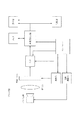
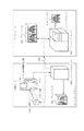
図1は、走査手段である水平、垂直シフトレジスタなどの周辺回路を有効画素領域内に作りこんだ撮像素子の構成を示す図である。図2は有効画素領域内の画素及びシフトレジスタ、保護回路、外部端子などのレイアウトを示す図である。図3、4、5は該撮像素子を9個張り合わせた撮像モジュ−ルを説明するための図である。図11は本実施の形態による撮像装置の構成を示すブロック図である。
【0009】
図11に示すように、被写体の動画像を得る場合は、放射線源であるパルスX線発生器100からX線パルスを発生させ、被写体を透過した撮像パネル101内のX線がシンチレータによって可視光に変換される。この光を撮像パネル101内の撮像素子で電気信号に変換する。アナログ量の電気信号はA/D変換器102によりディジタル信号に変換された後、画像処理回路103で画像処理が行われ、動画像を複数フレーム蓄積する記憶部106に蓄積される。そして、表示部105に画像が表示される。また、撮像素子は、センサ駆動部107によって、パルスX線装置100は、X線駆動部108によって駆動される。パルスX線発生器、撮像モジュ−ルの各撮像素子、画像処理装置の制御は制御手段であるコントローラ109で行っている。このコントローラへの入力操作には、操作装置、および操作モニタが用いられる。
【0010】
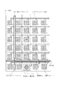
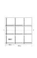
図4は138mm□の撮像素子を9枚タイル状に張り合わせて形成した414mm□の大面積撮像モジュ−ルの撮像素子部分を示す。
【0011】
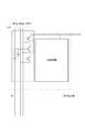
図5は図4のA−A’断面を示す。ユウロピウム、テルビウム等を付活性体として用いたGd2O2SやCsIなどのシンチレータからなるシンチレータ板をFOPの上に設置する。X線はシンチレータに当たり、可視光に変換される。この可視光を撮像素子で検出する。シンチレータは、その発光波長が撮像素子の感度に適合するように選択するのが好ましい。外部処理基板は撮像素子の電源、クロック等を供給し、又、撮像素子から信号を取り出して処理する回路を有する。TAB(Tape Automated Bonding)は、各撮像素子と外部処理基板とを電気的に接続する。
【0012】
9枚の撮像素子は、実質的に撮像素子間に隙間ができないように貼り合わせる。ここで実質的に隙間ができないこととは、9枚の撮像素子により形成される画像に撮像素子間の欠落ができないということである。撮像素子のクロック等や電源の入力、画素からの信号の出力は撮像素子端部に設けた電極パッドに接続したTABを通して、撮像素子の裏側に配置した外部処理基板との間で行う。TABの厚さは画素サイズに対して十分薄く撮像素子の間の隙間を通しても、画像上の欠陥は生じない。
【0013】
図3は現在主流の8インチウエハから一個の撮像素子を取り出す場合を示す。8インチウエハはN型ウエハであり、これを用い、CMOSプロセスによって138mm□のCMOS型撮像素子を1枚取りで作成する。
【0014】
図6にCMOS型撮像素子の各画素を構成する画素部の構成図を示す。光電変換をするフォトダイオードPD、電荷を蓄積するフローティングディフュージョンCFD、フォトダイオードが生成した電荷をフローティングディフュージョンに転送する転送MOSトランジスタ(転送スイッチ)、フローティングディフュージョンに蓄積された電荷を放電するためのリセットMOSトランジスタ(リセットスイッチ)、行選択をするための行選択MOSトランジスタ(行選択スイッチ)、ソースフォロワーとして機能する増幅MOSトランジスタ(画素アンプ)を有する。
【0015】
図7に3×3画素での全体回路の概略図を示す。
【0016】
転送スイッチのゲートは垂直走査回路の一種である垂直シフトレジスタからのφTXに接続され、リセットスイッチのゲートは垂直走査回路からのφRESに接続され、行選択スイッチのゲートは垂直走査回路からのφSELに接続されている。
【0017】
光電変換はフォトダイオードでおこなわれ、光量電荷の蓄積期間中は、転送スイッチはオフ状態であり、画素アンプを構成するソースフォロアのゲートにはこのフォトダイオードで光電変換された電荷は転送されない。該画素アンプを構成するソースフォロアのゲートは、蓄積開始前にリセットスイッチがオンし、適当な電圧に初期化されている。すなわちこれがダークレベルとなる。次に又は同時に行選択スイッチがオンになると、負荷電流源と画素アンプで構成されるソースフォロワー回路が動作状態になり、ここで転送スイッチをオンさせることで該フォトダイオードに蓄積されていた電荷は、該画素アンプを構成するソースフォロアのゲートに転送される。
【0018】
ここで選択行の出力が垂直出力線(信号出力線)上に発生する。この出力は列選択スイッチ(マルチプレクサ)を水平走査回路の一種である水平シフトレジスタによって駆動することにより順次出力部アンプへ読み出される。
【0019】
図2は垂直シフトレジスタの単位ブロック(一行を選択し駆動するための単位)を1画素領域(1セル)に1画素回路と共に配置した様子を示す。1画素回路は図6に示すものである。垂直シフトレジスタは転送信号φTX、リセット信号φRES、行選択信号φSELを作り出すためにスタティック型シフトレジスタと転送ゲートで構成した簡単な回路を示す。これらはクロック信号線(不図示)からの信号により駆動する。シフトレジスタの回路構成はこの限りではなく、画素加算や間引き読み出し等のさまざまな駆動のさせ方により、任意の回路構成をとることができる。ただし本実施形態のように機能ブロックを一つのセルの中に画素回路と共に配置し、有効画素領域内にシフトレジスタを設け、全面有効画素領域の撮像素子を実現する。
【0020】
本実施の形態においては、垂直シフトレジスタやn対2nデコーダ等の垂直走査回路、水平シフトレジスタやn対2nデコーダ等の水平走査回路を有効画素領域内の各画素領域(セル)内に配置することを特徴とする。
【0021】
同様に本実施の形態においては、共通処理回路を有効画素領域内の各画素領域(セル)内に配置することを特徴とする。ここで共通処理回路とは、最終信号出力アンプ、シリアル・パラレル変換マルチプレクサ、バッファー、各種ゲート回路等の複数画素を一括して共通に処理する回路を意味する。
【0022】
これに対して個別回路とは、フォトダイオード、転送スイッチ、画素選択スイッチ、画素出力増幅回路等の1画素のみを処理する回路を意味する。
【0023】
図1に本実施形態の撮像素子の構成(平面図)を示す。本実施形態では垂直シフトレジスタと水平シフトレジスタを撮像素子の有効画素領域に配置する。1つのラインを共通処理するシフトレジスタの1ブロックを1画素ピッチ内に収まるように配置する。これらのブロックを並べて一連の垂直シフトレジスタブロックとし、水平シフトレジスタブロックとする。これらのブロックは垂直方向、水平方向に直線状に伸びている。これらのシフトレジスタブロックのある画素の受光部の面積と、他の画素の受光部の面積は同じにし、感度のばらつきをなくす。さらに全ての受光部の重心(画素の重心)は同一とする。シフトレジスタとしてスタティックシフトレジスタを用いる。シフトレジスタの回路構成は、設計でいろいろなものが適用できる。この実施形態では一般的な回路例を取り上げた。
【0024】
本実施の形態によれば、撮像素子の周辺にデッドスペースが生じないので、撮像素子全面が有効画素領域となる。
【0025】
これらの撮像素子をタイル状に、実質的に隙間がないように並べることで、大板の撮像装置(フラットパネルディテクタ)を形成できる。実質的に繋ぎ目のない大板の画像を得ることができる。
【0026】
医療用のX線撮像装置では、画素の大きさは、100μm□〜200μm□程度に大きくてよいので、構成素子数の多いスタティックシフトレジスタを配置しても、十分大きい開口率を実現できる。
【0027】
また走査手段として、シフトレジスタではなく、n対2nデコーダを使用することもできる。デコーダの入力に順次インクリメントするカウンタの出力を接続することにより、シフトレジスタと同様に順次走査することが可能となり、一方、デコーダの入力に画像を得たい領域のアドレスを入力することにより、ランダム走査による任意の領域の画像を得ることができる。
【0028】
本実施形態は、撮像素子として、CMOS型撮像素子を用いているので、消費電力が少なく、大板の撮像装置を構成する場合に好適である。
【0029】
なお撮像素子内にマルチプレクサを作りこむのは、撮像素子での動作を早くするためである。
【0030】
また撮像素子からは電極パッドを経由して外部に信号を取り出すが、この電極パッド周りには大きな浮遊容量がある。従って電極パッドの前段にアンプを設けることにより、信号の伝送特性を補償することができる。
【0031】
本実施形態では、垂直、水平シフトレジスタを有効画素領域内に配置するので、シンチレータ板を抜けたX線が直接シフトレジスタに当たる。X線は、これらの回路中の素子にダメージを与えたりや回路中にエラーやノイズを生じたりするので問題である。
【0032】
エラーの例としてあげられるのは、絶縁酸化膜SiO2とシリコンの界面に電荷が蓄積され、閾値の変動やリーク電流の増加が起きる現象である。またダメージの例としてあげられるのは、pn接合面に生じる欠陥であり、この欠陥がリーク電流の増大を引き起こす。エラーの他の例としてあげられるのは、MOS型ダイナミックRAMでの誤動作として知られるホットエレクトロンの作用によるエラー(ソフトエラー)と同様なものである。例えば駆動用回路ではリセット回路にノイズが発生し、走査が一時的に停止したり、またシフトパルスがずれたりする。他の周辺回路では主にノイズとなる場合が多い。電界により発生するホットエレクトロンは、電界が高くなる短チャンネル構造で起こりやすいが、X線により発生するホットエレクトロンはサイズによらず発生するので、平面的なサイズによらずX線が当たると撮像装置は不安定になりやすい。ノイズとしては、単結晶シリコン中に進入したX線により、シリコン中に電子・ホール対を生成する。これらキャリアが回路中に侵入することにより生じるノイズがあり、回路が持つ固有のシステムノイズに付加される。このような現象はシフトレジスタばかりでなく、X線が直接の照射される可能性のあるデコーダや共通アンプなどの等の回路を用いる場合も発生する。
【0033】
FOPを用いることにより、撮像素子に直接進入するX線の量(X線フォトン数)を数十分の1以下にすることができる。X線のダメージは吸収したX線の総量に比例するので、FOPによりX線のダメージは相当低減することができる。一方X線によるエラーやノイズは、X線の総量ばかりでなく、X線のエネルギーにも依存する。80kVpの管電圧で発生したX線のエネルギーは、最大で80keV、平均で60keV程度と非常に大きい。この高エネルギーX線フォトンが1個でも吸収されると、数万個の電子・ホール対が発生する。これらが受光部に侵入すると、スパイク状の信号となり、同時にこの信号の揺らぎがノイズとして付加される。受光部以外の容量、信号線、トランジスタに侵入すると、ノイズ成分となり付加される。またシフトレジスタなどのロジック回路に侵入すると動作エラーの原因となる。つまりFOPのみでは、ダメージを低減することはできるが、エラーやノイズを低減することは難しい。
【0034】
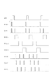
本発明では以下のような駆動を考慮することにより、直接的なX線によるノイズに強いX線撮像装置を実現できた。図8は本実施形態の撮像装置の動作を示すタイミングチャートである。3×3画素の動作で説明する。
【0035】
T1でリセット信号φRESがハイレベルになり、全画素のリセットMOSトランジスタがオンになることで、フローティングディフュージョンCFDがリセットされる。被写体撮像のためのX線パルスを照射し、フォトダイオードを露光する。全画素一括で転送信号φTXをハイレベルとし転送スイッチをオンすることで、フォトダイオードに蓄積されていた電荷を画素アンプを構成するソースフォロワーのゲート部に形成されるフローティングディフュージョンCFDに完全転送する。行選択信号SEL1がハイレベルになることで該当行の行選択MOSトランジスタがオンとなり、増幅MOSを介して信号出力線に撮像信号が読み出される。こうして読み出された1行分の撮像信号は、水平シフトレジスタにより列選択信号φSH1、φSH2、φSH3が順次オンになることで共通アンプを介して撮像素子の外部へ読み出される。同様に各行の信号が読み出される。本実施例ではX線のパルスはリセット信号φRESと転送信号φTXの間に照射する。X線がFOS画素領域全面に照射されている間、画素領域内に設置された水平シフトレジスタ、垂直シフトレジスタで駆動用信号を作り出すことはないので、これらが誤動作することはない。またX線によるノイズがこれらの回路に付加されることもない。
【0036】
これらの動作を行っているのは画素領域内に設置した垂直、水平シフトレジスタであり、これらの回路を駆動している間はX線は照射されず、これらが誤動作することはない。またこの間シリコンバルクに進入したX線によるキャリアの発生もなく、回路動作中にノイズが付加されることはない。また 画素加算等を画素毎に行うために、画素信号を加算して出力するための加算スイッチを設ける場合もある。このような場合には画素を共通に処理するため共通処理回路を画素領域内に設ける。この共通処理回路で加算等の動作を行う場合も、X線がオフの場合に行う。加算時、加算後の信号に直接X線によるノイズが付加されることはなく、共通処理回路が誤動作を起こすこともない。
【0037】
なお、以上説明した実施形態では、X線を可視光に変換するのに蛍光体を用いたが、一般的なシンチレータ、つまり波長変換体であればよい。また蛍光体がなくとも光電変換素子自身が直接放射線を検知し、電荷を発生するものでもよい。
【0038】
また、X線を用いた場合を例に説明したが、α、β、γ線等の放射線を用いることができる。
【0039】
(第2の実施形態)
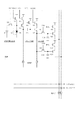
次に本発明の第2の実施形態について説明する。第2の実施形態で用いられる撮像素子は、基本構成は第1の実施形態と同じであるが、1画素の回路構成が第1の実施形態と異なっている。図9は本発明の第2の実施形態の1画素回路を示す。本実施形態では、光電変換部でのkTC補正を画素内で行うようにし、更に感度切替え手段を画素内に設けることで、静止画撮影と高速動画撮影をモード切替で実現している。
【0040】
ここで静止画撮影、動画撮影兼用の撮像素子での光電変換部に求められる特有の条件について説明する。動画撮影時の照射X線量は静止画撮影時の1/100程度であり、画素当たり高々数個のX線ホトンの量(実際画素に入射するのはこのX線が変換された可視光)であり、撮像素子としては最大の感度が求められる。但し、ダイナミックレンジは問題ない。更に、読取速度としては60から90フレーム/秒が求められる。画素の解像度は200μm□から400μm□と粗くともよい。一方、静止画撮影時には、80dB近いダイナミックレンジが要求される。画素の解像度は100μm□から200μm□が必要である。これらの仕様を同時に満たす撮像素子はこれまでなかった。
【0041】
そこで本実施形態では、CMOS型撮像素子において図9に示すような画素回路構成とすることで、これらの仕様を満たす撮像素子を実現している。図9において、PDは光電変換部としてのCCD等で用いられているものと同じ埋め込み型のフォトダイオードである。埋め込み型のフォトダイオードは表面に不純物濃度が高いp+層を設けることで、SiO2面で発生する暗電流を抑制するものである。またフォトダイオードPDの容量CPDは、動画撮影時に最大感度を得るために最小となるように設計している。後述するようにフォトダイオードPDの容量を小さくすると、ダイナミックレンジが縮小する。動画時に比べて照射X線量が100倍以上になる静止画撮影時にはダイナミックレンジが不足するので、ダイナミックレンジ拡大用の容量C1をフォトダイオードFDと並列に設けている。
【0042】
M1は静止画モード(高ダイナミックレンジ)と動画モード(高感度モード)を切り替える切り替えスイッチである。電荷を蓄積するフローティングディフュージョン(浮遊拡散領域)容量CFD(不図示)も動画時に最大感度となるよう最小容量に設計する。フローティングディフュージョン(浮遊拡散領域)は増幅MOSトランジスタM4のゲート部に接続して形成されている。M2はフローティングディフュージョンに蓄積された電荷を放電するためのリセットMOSトランジスタ(リセットスイッチ)、M3は画素アンプ1を選択をするための選択MOSトランジスタ(選択スイッチ)、M4はソースフォロワーとして機能する増幅MOSトランジスタ(画素アンプ1)である。
【0043】
この画素アンプ1の後段に本実施形態の特徴であるクランプ回路が設けられている。このクランプ回路により光電変換部で発生するkTCノイズを除去する。CCLはクランプ容量、M5はクランプスイッチである。クランプ回路の後に第1の実施形態と同様にサンプルホールド回路を設けている。M6は画素アンプ2を選択するための選択MOSトランジスタ(選択スイッチ)、M7はソースフォロワーとして機能する増幅MOSトランジスタ(画素アンプ2)である。M8は光信号蓄積用のサンプルホールド回路を構成するサンプルMOSトランジスタスイッチ、CH1はホールドコンデンサである。
【0044】
またM9は画素アンプ3を選択するための選択MOSトランジスタ(選択スイッチ)、M10はソースフォロワーとして機能する増幅MOSトランジスタ(画素アンプ3)である。M11はノイズ信号蓄積用のサンプルホールド回路を構成するサンプルMOSトランジスタスイッチ、CH2はホールドコンデンサである。M12は画素アンプ3を選択をするための選択MOSトランジスタ(選択スイッチ)、M13はソースフォロワーとして機能する増幅MOSトランジスタ(画素アンプ3)である。
【0045】
本実施形態においては、画素アンプでの熱ノイズ、1/fノイズ、温度差、プロセスばらつきによるFPNを除去するためにこれらの光信号、ノイズ用画素内サンプルホールド回路を用いている。
【0046】
次に画素部の構成について説明する。本実施形態では画素が160μm□と大きいため、適度な開口率(フォトダイオードの面積)で容量CPDを小さくするには限界がある。フォトダイオードの面積はそのままで電極面積を小さくする方法をとることで容量CPDを小さくできるが、この方法では電極への電荷の収集効率が落ち、転送スイッチにより信号電荷をフローティングディフュージョンへ完全転送することが困難になる。本実施形態では完全転送を行わない設計とし、転送スイッチは設けず、フォトダイオードとフローティングディフュージョンを直結し光電変換部としている。また動画撮影時に最高感度となるようにフォトダイオードの容量CPDとフローティングディフュージョンの容量CFDは最小となるように設計している。
【0047】
本実施形態では、完全転送ではないので光電変換部のリセット時にkTCノイズが発生してしまうが、回路的にこのkTCノイズ(リセットノイズ)を除去することは光電変換装置の高S/N化の重要なポイントとなる。そのため、本実施形態ではクランプ回路を画素毎に設ける構成としている。kTCノイズ除去のためにクランプ回路を用いることは公知である。画素のサイズが50から100μm□と比較的小さく完全転送が可能な場合は光電変換部でのkTCノイズは発生しないのでこの限りではない。
【0048】
しかしながら、静止画モードと動画モードを兼用する撮像素子とするためには、静止画モードでもkTCノイズの除去は必要であり、画素内にクランプ回路を設けることは必須となる。本実施形態では一括露光の動画モードでもkTCノイズを除去できるように一括露光用のサンプルホールド回路の前段にクランプ回路を設けている。
【0049】
また静止画撮影用にフォトダイオードのダイナミックレンジを大きくするためには容量CPDが大きい方が良いが、そうすると信号電圧が下がってしまうので、S/Nが下がってしまう。動画撮影時の最高感度を維持しながら静止画撮影時のダイナミックレンジを広げるために、感度(ダイナミックレンジ)切り替え回路を設け、容量と切り替えスイッチを本実施形態では各画素に設けている。静止画撮影時は容量が増えるのでS/Nが悪くなってしまうが、S/Nをよくするためには、特にkTCノイズを除去するクランプ回路が必要である。
【0050】
図10は本実施形態を動画モードで駆動している場合の画素部の動作を示すタイミングチャートである。図10を用いて、この撮像素子の駆動タイミングを説明する。
まず全画素一括で垂直シフトレジスタVSRからの信号φEN、φCHGをハイレベルとし、選択スイッチM3、M6をオンすること増幅トランジスタへの定電流源をオンし、信号φRESをハイレベルとしてフォトダイオードの電荷をリセット電位にリセットする。次に信号φCLをハイレベルとしてMOSトランジスタM5をオンすることで、クランプ容量の1端がクランプ電位にバイアスされる。こうしてフォトダイオードの電荷のリセットにより生じるkTCノイズ(リセットノイズ)をクランプ容量に蓄積する。また信号φTNをハイレベルとすると、クランプ容量のクランプ電位がノイズ用サンプルホールド容量CH2に蓄積される。以上がノイズ信号蓄積動作である。
【0051】
次にX線のパルス照射により露光が行われ、光電荷がフォトダイオードに蓄積される(これが露光動作である)。この後で信号φENをハイレベルにすると、クランプ容量の一端の電位は光電荷に対応する信号成分だけ変動する。すなわち、クランプ容量にはkTCノイズ成分が蓄積されているので、kTCノイズ成分を含む撮像信号からkTCノイズ成分が差し引かれた電位分クランプ容量の一端の電位が変動することになる。このkTCノイズのキャンセルされた撮像信号を読み出すため、信号CHGおよび信号φTSをハイレベル.にすることで、kTCノイズのキャンセルされた撮像信号(光信号)が信号用サンプルホールド容量に蓄積される。以上が光信号蓄積動作である。
【0052】
上記の一連の動作が繰り返される。ここで撮像素子の露光可能時間は、クランプ電位を容量に転送後、即ち信号ENがロウレベルになってから、信号φRESがハイレベルになりリセットMOSトランジスタがオンになる迄である。本実施形態では、特にこのX線パルスのタイミングと画素領域内に設置したシフトレジスタの駆動タイミングの関係に注目する。本実施形態では信号読み出しの間はX線を照射しない。図10に示すように信号読み出しを終わったあとから次のφENをオンする前にX線照射を行う。すなわちX線パルスが照射されていいない間に、各行ごとに信号φSELをハイレベルとし、さらに各列ごとに信号φSELHをハイレベルとすることで、ノイズ信号と光信号とが出力される。これらの駆動信号を作りだしているのは、垂直、水平シフトレジスタであり、これらのシフトレジスタが信号を作り出している間は、X線は照射されない。つまりX線パルスが照射されてフォトダイオードが露光されている間は、シフトレジスタによる画素内の素子の駆動は行われない。よってX線パルスが撮像素子に直接進入した場合、シフトレジスタでエラー(誤動作)が起こったり、信号転送中にノイズが乗ったりすることがない。
【0053】
ノイズ信号出力線と光信号出力線に転送された信号はノイズ信号出力線と光信号出力線とに接続された減算出力アンプ(図示せず)で、(信号−ノイズ)の減算処理を行う。この時、光信号とノイズ信号は非常に速い時間差で、画素アンプ2からサンプルホールド回路に取り込まれるので、低周波数で値の大きい1/fノイズを除去でき、高周波の成分は無視できる。またこの時間差では出力段ソースフォロワーの温度差による閾値Vthのばらつきもない。ホールド容量に蓄えられていた出力電荷は、1個の画素アンプについての、リセット時と信号電荷入力時の両者の場合の出力を時間的に連続して得たものであり、更にこれら両出力の差分をとることにより、画素アンプでの熱ノイズ、1/fノイズ、温度差、プロセスばらつきによるFPNを除去することができる。
【0054】
一方、静止画モードでは、信号φSCをハイレベルとし、容量C1をフォトダイオードPDに並列接続した段階で、上記と同様な動作を行う。この場合、容量C1には容量CFDの10倍近い容量を持たせているので、広いダイナミックレンジを実現できる。また光電変換部のkTCノイズはクランプ回路により画素毎に除去できる。更に、画素中に光信号蓄積用、ノイズ信号蓄積用のサンプルホールド回路を設けることで、画素アンプでの熱ノイズ、1/fノイズ、温度差、プロセスばらつきによるFPNを除去することができる。これにより、動画モードでは9枚の撮像素子で時間的、空間的に繋ぎ目のない高速、高感度の動画像撮影を実現できる。一方、静止画モードでは高感度、高ダイナミックレンジの静止画像撮影を実現できる。
【0055】
これらの動作を行っているのは画素領域内に設置した垂直、水平シフトレジスタであり、これらの回路を駆動している間はX線は照射されず、これらが誤動作することはない。またこの間シリコンバルクに進入したX線によるキャリアの発生もなく、回路動作中にノイズが付加されることはない。また 画素加算等を画素毎に行うために、画素信号を加算して出力するための加算スイッチを設ける場合もある。このような場合には画素を共通に処理するため共通処理回路を画素領域内に設ける。この共通処理回路で加算等の動作を行う場合も、X線がオフの場合に行う。加算時、加算後の信号に直接X線によるノイズが付加されることはなく、共通処理回路が誤動作を起こすこともない。
【0056】
本実施例では信号用とノイズ用のサンプルホールド回路を有している。これらの回路に信号が蓄積されている場合に、X線が照射されるとこれらの回路中でノイズが発生し画質を低下させるおそれがある。よって好適にはこれらのサンプルホールド回路に信号が蓄積されている間にはX線パルスを照射しないようにする。
【0057】
なお、以上説明した各実施形態では、X線を可視光に変換するのに蛍光体を用いたが、一般的なシンチレータ、つまり波長変換体であればよい。また蛍光体がなくとも光電変換素子自身が直接放射線を検知し、電荷を発生するものでもよい。
また各実施形態では、X線を用いた場合を例に説明したが、α、β、γ線等の放射線を用いることができる。
【0058】
以上のように、第1、第2の実施の形態では、パルスX線発生器100からの所定間隔で発生する放射線パルスが発生していない期間に、垂直、水平シフトレジスタ等の走査手段が撮像領域を走査するように、センサ駆動部107、X線駆動部108を制御するコントロ−ラ119を有することにより、良好な画像を得ることが可能となる。
【0059】
(第3の実施形態)
図12は、実施の形態1、2で説明した撮像装置のX線診断システムへの応用例を示したものである。
【0060】
X線チューブ6050で発生したX線6060は患者あるいは被験者6061の胸部6062を透過し、シンチレータ、FOP、撮像素子、外部処理基板を備える放射線撮像装置6040に入射する。この入射したX線には患者6061の体内部の情報が含まれている。X線の入射に対応してシンチレータは発光し、これを撮像素子が光電変換して、電気的情報を得る。この情報はディジタルに変換されイメージプロセッサ6070により画像処理され制御室のディスプレイ6080で観察できる。
【0061】
またこの情報は電話回線6090等の伝送手段により遠隔地へ転送でき、別の場所のドクタールームなどディスプレイ6081に表示もしくは光ディスク等の保存手段に保存することができ、遠隔地の医師が診断することも可能である。またフィルムプロセッサ6100によりフィルム6110に記録することもできる。
【0062】
【発明の効果】
以上説明したように、本発明にかかる撮像装置によれば、高品質の動画像を得ることが可能となる。
【図面の簡単な説明】
【図1】撮像素子のレイアウトを示す平面図である。
【図2】撮像素子内の1画素回路とシフトレジスタの単位ブロックの関係を示す図である。
【図3】撮像素子とその元となるウエハを示す平面図である。
【図4】撮像モジュ−ルにおける撮像素子の配列及び走査回路の配列を示す平面図である。
【図5】撮像モジュ−ルの構成を示す断面図であり、図4のA−A’断面を示す。
【図6】本発明の第1の実施形態による撮像素子の1画素回路図である。
【図7】本発明の第1の実施形態による撮像素子における等価回路である。
【図8】本発明の第1の実施形態における動作タイミングである。
【図9】本発明の第2の実施形態による撮像素子の1画素回路図である。
【図10】本発明の第2の実施形態における動作タイミングである。
【図11】撮像装置のブロック図である。
【図12】放射線撮影システムの構成を示す概念図である。
【図13】第1の従来の技術をあらわす図である。
【図14】第2の従来の技術をあらわす図である。
【図15】第3の従来の技術をあらわす図である。
【符号の説明】
100 パルスX線装置
101 撮像モジュ−ル
107 センサ駆動部
108 X線駆動部
109 コントロ−ラ[0001]
BACKGROUND OF THE INVENTION
The present invention relates to an imaging apparatus used for radiological medical equipment and the like.
[0002]
[Prior art]
Digitization is progressing in various fields of medicine. Also in the field of X-ray diagnosis, in order to digitize an image, a two-dimensional X-ray imaging apparatus that converts incident X-rays into visible light by a scintillator (phosphor) and further captures the visible light image with an image sensor. It has been developed. Advantages of the digitized X-ray imaging apparatus over the analog photographic technique include the following. These include filmlessness, expansion of acquired information through image processing, and creation of a database. In addition, it is useful in an urgent medical site that the captured image can be displayed instantaneously on the spot. Radiation means X-rays, α, β, γ rays, or high energy rays that can detect the internal structure of the subject, and light is an electromagnetic wave in a wavelength region that can be easily detected by a photoelectric conversion means such as a photodiode. Including visible light and infrared light. The case of X-rays as radiation will be described below.
[0003]
In the field of X-ray still images, as a two-dimensional X-ray imaging device, for example, a large-plate still image imaging device (flat) using amorphous silicon (a-Si) having a maximum of 43 cm □ for mammography and chest imaging. Panel detector) is made. An example of this type of technique is described in US Pat. No. 5,315,101. This conventional technique is shown in FIG. An image pickup device using an amorphous silicon semiconductor on a glass substrate is easy to obtain a large plate, and there is one that realizes a large plate X-ray image pickup device by tiling four panels. There is also a proposal for constructing a large X-ray imaging apparatus using a plurality of single crystal imaging elements (such as silicon imaging elements). An example of this type of technique is US Pat. No. 4,323,925, 5159455 shown in FIG. Examples of the single crystal imaging device include a CCD type imaging device using silicon, a MOS type imaging device, a CMOS type imaging device, and the like. A fiber optic plate (FOP) with a phosphor is used as the X-ray converter. The fiber optic plate is made of a material containing lead glass or the like that hardly transmits X-rays. In general, a single crystal silicon device such as a CCD is easily damaged by radiation such as X-rays and causes deterioration such as an increase in dark current and a decrease in photoelectric conversion efficiency. Therefore, a fiber optic plate is used as an X-ray shielding material. As a result, the X-ray resistance is increased and the reliability is improved. In a conventional CCD type image pickup device, MOS type image pickup device, or CMOS type image pickup device, a circuit (shift register, decoder, multiplexer, etc.) or memory circuit for driving the device is arranged on the outer periphery of the pixel region of the device. FIG. 13 shows a case where four CMOS image sensors are bonded. Since these circuits also cause malfunctions and deterioration when X-rays directly enter as in the pixel portion, they are generally configured to shield X-rays using lead or the like.
[0004]
In the field of X-ray animation, incident X-rays are converted into scintillators (phosphors) and I.D. I. A two-dimensional digital X-ray fluoroscopic apparatus has been developed that converts visible light by (image intensifier) and captures the visible light image with a TV camera using a CCD type imaging device. This is not a flat panel detector.
[0005]
In the field of medical X-ray diagnostics, which is becoming increasingly digitized, next-generation moving image capturing devices (such as fluoroscopy) that have been reduced in size, increased in sensitivity, and increased in speed by flat panels are expected.
[0006]
[Problems to be solved by the invention]
A radiation imaging apparatus (flat panel detector) using amorphous silicon (a-Si) can be easily made large, but it is difficult to achieve high sensitivity and high speed due to the characteristics of the amorphous silicon material. Therefore, it is limited to still images. A radiographic imaging device combining single crystal silicon and FOP can easily achieve high speed and high sensitivity, but it is inevitable to reduce the cost because a very expensive tapered FOP must be used for large plate. Therefore, there has been no X-ray imaging apparatus that is fully equipped with large plates, high speed, high definition, high sensitivity, and low cost. Furthermore, in order to reduce the influence of X-rays in single crystal silicon, there has been no driving considering the relationship between driving of X-ray pulses and X-ray noise caused by direct incidence.
[0007]
[Means for Solving the Problems]
To solve the above problem, Are generated sequentially at predetermined intervals, Transmitted through the subject radiation Converted light For converting to electrical signals Multiple pixels Each of the plurality of pixels includes a photoelectric conversion unit, a signal sample-and-hold circuit for storing the electric signal, and a noise sample-and-hold circuit for storing a noise signal. An imaging area; Arranged between pixels in the imaging region, Scanning means for scanning the imaging region, and a period in which the radiation is not generated, The electrical signal is output from the signal sample and hold circuit, and the noise signal is output from the noise sample and hold circuit. Said scanning means by The imaging area of scanning The And an image pickup apparatus characterized by comprising a control means for controlling.
[0008]
DETAILED DESCRIPTION OF THE INVENTION
(First embodiment)
FIG. 1 is a diagram showing a configuration of an image sensor in which peripheral circuits such as horizontal and vertical shift registers as scanning means are formed in an effective pixel region. FIG. 2 is a diagram showing a layout of pixels in the effective pixel region, a shift register, a protection circuit, an external terminal, and the like. 3, 4, and 5 are diagrams for explaining an imaging module in which nine imaging elements are bonded together. FIG. 11 is a block diagram showing the configuration of the imaging apparatus according to this embodiment.
[0009]
As shown in FIG. 11, when a moving image of a subject is obtained, an X-ray pulse is generated from a pulse X-ray generator 100 that is a radiation source, and X-rays in the imaging panel 101 that have passed through the subject are made visible by a scintillator. Is converted to This light is converted into an electrical signal by an image sensor in the image pickup panel 101. The analog electric signal is converted into a digital signal by the A / D converter 102, then subjected to image processing by the image processing circuit 103, and stored in the storage unit 106 that stores a plurality of moving images. Then, an image is displayed on the display unit 105. The imaging element is driven by the sensor driving unit 107, and the pulse X-ray apparatus 100 is driven by the X-ray driving unit 108. Control of the pulse X-ray generator, each imaging device of the imaging module, and the image processing apparatus is performed by a controller 109 which is a control means. For the input operation to the controller, an operating device and an operation monitor are used.
[0010]
FIG. 4 shows an image pickup element portion of a large area image pickup module of 414 mm □ formed by sticking nine 138 mm □ image pickup elements in a tile shape.
[0011]
FIG. 5 shows an AA ′ cross section of FIG. Gd using europium, terbium, etc. as an activator 2 O 2 A scintillator plate made of a scintillator such as S or CsI is placed on the FOP. X-rays hit the scintillator and are converted into visible light. This visible light is detected by the image sensor. The scintillator is preferably selected so that its emission wavelength matches the sensitivity of the image sensor. The external processing board has a circuit for supplying power to the image sensor, a clock, and the like, and extracting and processing signals from the image sensor. TAB (Tape Automated Bonding) electrically connects each image sensor to an external processing board.
[0012]
The nine image sensors are bonded so that there is substantially no gap between the image sensors. Here, the fact that there is substantially no gap means that an image formed by nine image sensors cannot be lost between the image sensors. The clock of the image sensor, power supply input, and signal output from the pixel are performed with an external processing substrate disposed on the back side of the image sensor through a TAB connected to an electrode pad provided at the end of the image sensor. Even if the thickness of the TAB is sufficiently small with respect to the pixel size and passes through the gap between the image pickup elements, no defect on the image occurs.
[0013]
FIG. 3 shows a case where one image pickup device is taken out from the currently mainstream 8-inch wafer. The 8-inch wafer is an N-type wafer, and using this, a 138 mm □ CMOS-type image sensor is produced by a single process by a CMOS process.
[0014]
FIG. 6 shows a configuration diagram of a pixel portion constituting each pixel of the CMOS image sensor. Photodiode PD for photoelectric conversion, floating diffusion C for storing charge FD , A transfer MOS transistor (transfer switch) for transferring the charge generated by the photodiode to the floating diffusion, a reset MOS transistor (reset switch) for discharging the charge accumulated in the floating diffusion, and a row selection MOS for selecting a row A transistor (row selection switch) and an amplification MOS transistor (pixel amplifier) functioning as a source follower are included.
[0015]
FIG. 7 shows a schematic diagram of the entire circuit with 3 × 3 pixels.
[0016]
The gate of the transfer switch is connected to φTX from a vertical shift register which is a kind of vertical scanning circuit, the gate of the reset switch is connected to φRES from the vertical scanning circuit, and the gate of the row selection switch is connected to φSEL from the vertical scanning circuit. It is connected.
[0017]
Photoelectric conversion is performed by a photodiode, and the transfer switch is in an OFF state during a light amount charge accumulation period. Charges photoelectrically converted by the photodiode are not transferred to the gate of the source follower constituting the pixel amplifier. The gate of the source follower constituting the pixel amplifier is initialized to an appropriate voltage by turning on the reset switch before starting the accumulation. That is, this is a dark level. Next or at the same time, when the row selection switch is turned on, the source follower circuit composed of the load current source and the pixel amplifier is activated, and the charge stored in the photodiode is changed by turning on the transfer switch here. And transferred to the gate of the source follower constituting the pixel amplifier.
[0018]
Here, the output of the selected row is generated on the vertical output line (signal output line). This output is sequentially read out to the output unit amplifier by driving a column selection switch (multiplexer) by a horizontal shift register which is a kind of horizontal scanning circuit.
[0019]
FIG. 2 shows a state in which unit blocks (units for selecting and driving one row) of a vertical shift register are arranged together with one pixel circuit in one pixel region (one cell). One pixel circuit is shown in FIG. The vertical shift register is a simple circuit composed of a static shift register and a transfer gate for generating a transfer signal φTX, a reset signal φRES, and a row selection signal φSEL. These are driven by signals from a clock signal line (not shown). The circuit configuration of the shift register is not limited to this, and an arbitrary circuit configuration can be adopted depending on various driving methods such as pixel addition and thinning readout. However, as in the present embodiment, the functional block is arranged together with the pixel circuit in one cell, and a shift register is provided in the effective pixel region, thereby realizing an imaging device in the entire effective pixel region.
[0020]
In this embodiment, a vertical shift register or n-to-2 n Vertical scanning circuit such as decoder, horizontal shift register and n-to-2 n A horizontal scanning circuit such as a decoder is arranged in each pixel region (cell) in the effective pixel region.
[0021]
Similarly, the present embodiment is characterized in that the common processing circuit is arranged in each pixel region (cell) in the effective pixel region. Here, the common processing circuit means a circuit that collectively processes a plurality of pixels such as a final signal output amplifier, a serial / parallel conversion multiplexer, a buffer, and various gate circuits.
[0022]
On the other hand, the individual circuit means a circuit that processes only one pixel, such as a photodiode, a transfer switch, a pixel selection switch, and a pixel output amplifier circuit.
[0023]
FIG. 1 shows the configuration (plan view) of the image sensor of this embodiment. In this embodiment, the vertical shift register and the horizontal shift register are arranged in the effective pixel area of the image sensor. One block of the shift register that processes one line in common is arranged so as to be within one pixel pitch. These blocks are arranged to form a series of vertical shift register blocks and to be a horizontal shift register block. These blocks extend linearly in the vertical and horizontal directions. The areas of the light receiving portions of the pixels having these shift register blocks are the same as the areas of the light receiving portions of the other pixels, so that variations in sensitivity are eliminated. Furthermore, the center of gravity (pixel center of gravity) of all the light receiving units is the same. A static shift register is used as the shift register. Various circuit configurations of the shift register can be applied by design. In this embodiment, a general circuit example is taken up.
[0024]
According to the present embodiment, since no dead space is generated around the image sensor, the entire surface of the image sensor is an effective pixel region.
[0025]
By arranging these image pickup elements in a tile shape so that there is substantially no gap, a large-plate image pickup device (flat panel detector) can be formed. An image of a large plate that is substantially seamless can be obtained.
[0026]
In a medical X-ray imaging apparatus, the size of a pixel may be as large as about 100 μm □ to 200 μm □, so that a sufficiently large aperture ratio can be realized even if a static shift register having a large number of components is arranged.
[0027]
The scanning means is not a shift register, but n-to-2. n A decoder can also be used. By connecting the output of the counter that sequentially increments to the input of the decoder, it becomes possible to scan sequentially as in the shift register, while at the same time, random scanning is performed by inputting the address of the area where the image is to be obtained to the input of the decoder. An image of an arbitrary region can be obtained.
[0028]
Since this embodiment uses a CMOS image sensor as the image sensor, it consumes less power and is suitable for configuring a large-sized image sensor.
[0029]
The reason why the multiplexer is built in the image sensor is to speed up the operation of the image sensor.
[0030]
A signal is taken out from the image pickup device via the electrode pad, and there is a large stray capacitance around the electrode pad. Therefore, by providing an amplifier in front of the electrode pad, signal transmission characteristics can be compensated.
[0031]
In the present embodiment, since the vertical and horizontal shift registers are arranged in the effective pixel region, the X-rays that have passed through the scintillator plate directly hit the shift register. X-rays are problematic because they damage elements in these circuits and cause errors and noise in the circuits.
[0032]
An example of an error is an insulating oxide film SiO 2 This is a phenomenon in which charges are accumulated at the interface between silicon and silicon, resulting in threshold fluctuations and increase in leakage current. An example of damage is a defect generated on the pn junction surface, and this defect causes an increase in leakage current. Another example of the error is the same as an error (soft error) caused by the action of hot electrons known as a malfunction in the MOS type dynamic RAM. For example, in the driving circuit, noise is generated in the reset circuit, and the scanning is temporarily stopped or the shift pulse is shifted. In other peripheral circuits, noise is often the main cause. Hot electrons generated by an electric field are likely to occur in a short channel structure in which the electric field is high. However, hot electrons generated by an X-ray are generated regardless of the size. Tends to be unstable. As noise, an electron / hole pair is generated in silicon by X-rays entering single crystal silicon. There is noise generated when these carriers enter the circuit, and it is added to the inherent system noise of the circuit. Such a phenomenon occurs not only in the shift register but also in the case of using a circuit such as a decoder or a common amplifier that may be directly irradiated with X-rays.
[0033]
By using FOP, the amount of X-rays (X-ray photon number) that directly enters the image sensor can be reduced to several tenths or less. Since X-ray damage is proportional to the total amount of absorbed X-rays, FOP can significantly reduce X-ray damage. On the other hand, errors and noise due to X-rays depend not only on the total amount of X-rays but also on the energy of the X-rays. The energy of X-rays generated at a tube voltage of 80 kVp is very large, about 80 keV at maximum and about 60 keV on average. If even one high-energy X-ray photon is absorbed, tens of thousands of electron / hole pairs are generated. When they enter the light receiving section, they become spike-like signals, and at the same time, fluctuations in the signals are added as noise. When it enters a capacitor, signal line, or transistor other than the light receiving portion, it is added as a noise component. Intrusion into a logic circuit such as a shift register causes an operation error. In other words, with FOP alone, damage can be reduced, but it is difficult to reduce errors and noise.
[0034]
In the present invention, an X-ray imaging apparatus resistant to noise caused by direct X-rays can be realized by considering the following driving. FIG. 8 is a timing chart showing the operation of the imaging apparatus of the present embodiment. The operation will be described with 3 × 3 pixels.
[0035]
At T1, the reset signal φRES becomes high level, and the reset MOS transistors of all the pixels are turned on, so that the floating diffusion C FD Is reset. An X-ray pulse for imaging a subject is irradiated and the photodiode is exposed. By turning on the transfer switch by setting the transfer signal φTX to the high level for all the pixels at once, the floating diffusion C formed in the gate portion of the source follower that constitutes the pixel amplifier is stored in the photodiode. FD To complete transfer. When the row selection signal SEL1 becomes high level, the row selection MOS transistor of the corresponding row is turned on, and the imaging signal is read to the signal output line via the amplification MOS. The image signals for one row read out in this way are read out of the image sensor through the common amplifier when the column selection signals φSH1, φSH2, and φSH3 are sequentially turned on by the horizontal shift register. Similarly, the signal of each row is read out. In this embodiment, the X-ray pulse is applied between the reset signal φRES and the transfer signal φTX. While the X-rays are irradiated on the entire surface of the FOS pixel area, the horizontal shift register and the vertical shift register installed in the pixel area do not generate drive signals, so that they do not malfunction. Further, noise due to X-rays is not added to these circuits.
[0036]
These operations are performed by the vertical and horizontal shift registers installed in the pixel region, and X-rays are not irradiated while these circuits are driven, and they do not malfunction. During this time, no carriers are generated by X-rays entering the silicon bulk, and no noise is added during circuit operation. In order to perform pixel addition for each pixel, an addition switch for adding and outputting pixel signals may be provided. In such a case, a common processing circuit is provided in the pixel region in order to process pixels in common. The common processing circuit performs an operation such as addition when the X-ray is off. At the time of addition, noise due to X-rays is not directly added to the signal after addition, and the common processing circuit does not malfunction.
[0037]
In the embodiment described above, a phosphor is used to convert X-rays into visible light. However, a general scintillator, that is, a wavelength converter may be used. Further, even if there is no phosphor, the photoelectric conversion element itself may directly detect radiation and generate a charge.
[0038]
Moreover, although the case where X-rays are used has been described as an example, radiation such as α, β, and γ rays can be used.
[0039]
(Second Embodiment)
Next, a second embodiment of the present invention will be described. The image sensor used in the second embodiment has the same basic configuration as that of the first embodiment, but the circuit configuration of one pixel is different from that of the first embodiment. FIG. 9 shows a one-pixel circuit according to the second embodiment of the present invention. In the present embodiment, kTC correction in the photoelectric conversion unit is performed in the pixel, and sensitivity switching means is provided in the pixel, so that still image shooting and high-speed moving image shooting are realized by mode switching.
[0040]
Here, the specific conditions required for the photoelectric conversion unit in the image sensor for both still image shooting and moving image shooting will be described. The irradiation X-ray dose at the time of moving image shooting is about 1/100 of that at the time of still image shooting, and the amount of X-ray photons at most per pixel (actually incident on this pixel is the visible light converted from this X-ray). There is a need for maximum sensitivity as an image sensor. However, there is no problem with the dynamic range. Further, a reading speed of 60 to 90 frames / second is required. The pixel resolution may be as coarse as 200 μm □ to 400 μm □. On the other hand, a dynamic range close to 80 dB is required during still image shooting. The pixel resolution needs to be 100 μm □ to 200 μm □. There has been no image sensor that satisfies these specifications at the same time.
[0041]
Therefore, in the present embodiment, an image sensor satisfying these specifications is realized by adopting a pixel circuit configuration as shown in FIG. 9 in the CMOS image sensor. In FIG. 9, PD is the same embedded photodiode used in a CCD or the like as a photoelectric conversion unit. The buried photodiode has a high impurity concentration on the surface. + By providing a layer, SiO 2 This suppresses dark current generated on the surface. The capacitance C of the photodiode PD PD Is designed to be minimized to obtain maximum sensitivity when shooting movies. Photodiode as described below PD Decreasing the capacity reduces the dynamic range. Since a dynamic range is insufficient at the time of still image shooting in which the irradiation X-ray dose is 100 times or more compared with that at the time of moving images, a capacitor C1 for expanding the dynamic range is provided in parallel with the photodiode FD.
[0042]
M1 is a changeover switch for switching between a still image mode (high dynamic range) and a moving image mode (high sensitivity mode). Floating diffusion (floating diffusion region) capacitance C for storing charge FD (Not shown) is also designed to have a minimum capacity so that the maximum sensitivity is obtained during moving images. The floating diffusion (floating diffusion region) is formed connected to the gate portion of the amplification MOS transistor M4. M2 is a reset MOS transistor (reset switch) for discharging charges accumulated in the floating diffusion, M3 is a selection MOS transistor (selection switch) for selecting the pixel amplifier 1, and M4 is an amplification MOS functioning as a source follower. This is a transistor (pixel amplifier 1).
[0043]
A clamp circuit, which is a feature of the present embodiment, is provided at the subsequent stage of the pixel amplifier 1. This clamp circuit removes kTC noise generated in the photoelectric conversion unit. C CL Is a clamp capacitor, and M5 is a clamp switch. A sample and hold circuit is provided after the clamp circuit as in the first embodiment. M6 is a selection MOS transistor (selection switch) for selecting the
[0044]
M9 is a selection MOS transistor (selection switch) for selecting the pixel amplifier 3, and M10 is an amplification MOS transistor (pixel amplifier 3) functioning as a source follower. M11 is a sample MOS transistor switch constituting a sample and hold circuit for accumulating noise signals, and CH2 is a hold capacitor. M12 is a selection MOS transistor (selection switch) for selecting the pixel amplifier 3, and M13 is an amplification MOS transistor (pixel amplifier 3) functioning as a source follower.
[0045]
In the present embodiment, in order to remove FPN due to thermal noise, 1 / f noise, temperature difference, and process variation in the pixel amplifier, these optical signals and the in-pixel sample and hold circuit for noise are used.
[0046]
Next, the configuration of the pixel portion will be described. In this embodiment, since the pixel is as large as 160 μm □, the capacitance C with an appropriate aperture ratio (photodiode area). PD There is a limit to making it smaller. Capacitance C can be obtained by reducing the electrode area while keeping the photodiode area unchanged. PD However, in this method, the efficiency of collecting charges on the electrodes is lowered, and it becomes difficult to completely transfer the signal charges to the floating diffusion by the transfer switch. In this embodiment, the design is such that complete transfer is not performed, no transfer switch is provided, and a photodiode and a floating diffusion are directly connected to form a photoelectric conversion unit. In addition, the capacitance C of the photodiode is set so that the maximum sensitivity is obtained when shooting a movie. PD And the capacity C of the floating diffusion FD Is designed to be minimal.
[0047]
In the present embodiment, since the transfer is not complete, kTC noise is generated when the photoelectric conversion unit is reset. However, removing this kTC noise (reset noise) in terms of the circuit can increase the S / N ratio of the photoelectric conversion device. It becomes an important point. Therefore, in this embodiment, a clamp circuit is provided for each pixel. It is known to use a clamp circuit to remove kTC noise. If the pixel size is relatively small, such as 50 to 100 μm □, and complete transfer is possible, kTC noise does not occur in the photoelectric conversion unit, so this is not the case.
[0048]
However, in order to obtain an image sensor that uses both the still image mode and the moving image mode, it is necessary to remove kTC noise even in the still image mode, and it is essential to provide a clamp circuit in the pixel. In the present embodiment, a clamp circuit is provided before the sample-and-hold circuit for batch exposure so that kTC noise can be removed even in the batch exposure moving image mode.
[0049]
In order to increase the dynamic range of the photodiode for still image shooting, the capacitance C PD Is better, but the signal voltage will decrease, and the S / N will decrease. In order to expand the dynamic range at the time of still image shooting while maintaining the highest sensitivity at the time of moving image shooting, a sensitivity (dynamic range) switching circuit is provided, and a capacitor and a changeover switch are provided in each pixel in this embodiment. Since the capacity increases during still image shooting, the S / N deteriorates, but in order to improve the S / N, a clamp circuit that specifically removes kTC noise is necessary.
[0050]
FIG. 10 is a timing chart showing the operation of the pixel portion when the present embodiment is driven in the moving image mode. The drive timing of this image sensor will be described with reference to FIG.
First, the signals φEN and φCHG from the vertical shift register VSR are set to the high level for all the pixels, the selection switches M3 and M6 are turned on, the constant current source to the amplification transistor is turned on, and the signal φRES is set to the high level to charge the photodiode. To the reset potential. Next, the signal φCL is set to the high level to turn on the MOS transistor M5, whereby one end of the clamp capacitor is biased to the clamp potential. In this way, kTC noise (reset noise) generated by resetting the charge of the photodiode is accumulated in the clamp capacitor. When the signal φTN is set to the high level, the clamp potential of the clamp capacitor is accumulated in the noise sample hold capacitor CH2. The above is the noise signal accumulation operation.
[0051]
Next, exposure is performed by X-ray pulse irradiation, and photoelectric charges are accumulated in the photodiode (this is an exposure operation). Thereafter, when the signal φEN is set to a high level, the potential at one end of the clamp capacitor changes by a signal component corresponding to the photocharge. That is, since the kTC noise component is accumulated in the clamp capacitor, the potential of one end of the clamp capacitor varies by the potential obtained by subtracting the kTC noise component from the imaging signal including the kTC noise component. In order to read out the imaging signal with the kTC noise canceled, the signal CHG and the signal φTS are set to the high level. By doing so, the imaging signal (optical signal) from which kTC noise has been canceled is accumulated in the signal sample-and-hold capacitor. The above is the optical signal accumulation operation.
[0052]
The above series of operations is repeated. Here, the exposure time of the image sensor is after the clamp potential is transferred to the capacitor, that is, from when the signal EN becomes low level until the signal φRES becomes high level and the reset MOS transistor is turned on. In the present embodiment, attention is particularly paid to the relationship between the timing of the X-ray pulse and the drive timing of the shift register installed in the pixel region. In this embodiment, X-rays are not irradiated during signal readout. As shown in FIG. 10, X-ray irradiation is performed after the signal readout is finished and before the next φEN is turned on. That is, while the X-ray pulse is not irradiated, the signal φSEL is set to a high level for each row, and the signal φSELH is set to a high level for each column, whereby a noise signal and an optical signal are output. These drive signals are generated by vertical and horizontal shift registers, and X-rays are not irradiated while these shift registers generate signals. In other words, while the X-ray pulse is irradiated and the photodiode is exposed, the element in the pixel is not driven by the shift register. Therefore, when the X-ray pulse directly enters the image sensor, an error (malfunction) does not occur in the shift register and noise does not occur during signal transfer.
[0053]
The signal transferred to the noise signal output line and the optical signal output line is subjected to a (signal-noise) subtraction process by a subtraction output amplifier (not shown) connected to the noise signal output line and the optical signal output line. At this time, the optical signal and the noise signal are taken into the sample hold circuit from the
[0054]
On the other hand, in the still image mode, the same operation as described above is performed when the signal φSC is set to the high level and the capacitor C1 is connected in parallel to the photodiode PD. In this case, the capacity C1 includes the capacity C FD Because it has a capacity that is nearly 10 times larger than the above, a wide dynamic range can be realized. Further, kTC noise in the photoelectric conversion unit can be removed for each pixel by a clamp circuit. Further, by providing a sample hold circuit for storing optical signals and noise signals in the pixel, it is possible to remove FPN caused by thermal noise, 1 / f noise, temperature difference, and process variation in the pixel amplifier. Thereby, in the moving image mode, it is possible to realize high-speed and high-sensitivity moving image shooting that is temporally and spatially seamless with nine image sensors. On the other hand, the still image mode can realize still image shooting with high sensitivity and high dynamic range.
[0055]
These operations are performed by the vertical and horizontal shift registers installed in the pixel region, and X-rays are not irradiated while these circuits are driven, and they do not malfunction. During this time, no carriers are generated by X-rays entering the silicon bulk, and no noise is added during circuit operation. In order to perform pixel addition for each pixel, an addition switch for adding and outputting pixel signals may be provided. In such a case, a common processing circuit is provided in the pixel region in order to process pixels in common. The common processing circuit performs an operation such as addition when the X-ray is off. At the time of addition, noise due to X-rays is not directly added to the signal after addition, and the common processing circuit does not malfunction.
[0056]
In this embodiment, signal and noise sample and hold circuits are provided. When signals are accumulated in these circuits, if X-rays are irradiated, noise may be generated in these circuits and the image quality may be deteriorated. Therefore, it is preferable not to irradiate X-ray pulses while signals are accumulated in these sample and hold circuits.
[0057]
In each of the embodiments described above, a phosphor is used to convert X-rays into visible light. However, a general scintillator, that is, a wavelength converter may be used. Further, even if there is no phosphor, the photoelectric conversion element itself may directly detect radiation and generate a charge.
In each embodiment, the case where X-rays are used has been described as an example, but radiation such as α, β, and γ rays can be used.
[0058]
As described above, in the first and second embodiments, scanning means such as vertical and horizontal shift registers capture images during a period in which no radiation pulse is generated from the pulse X-ray generator 100 at a predetermined interval. By having the controller 119 for controlling the sensor driving unit 107 and the X-ray driving unit 108 so as to scan the region, it is possible to obtain a good image.
[0059]
(Third embodiment)
FIG. 12 shows an application example of the imaging apparatus described in the first and second embodiments to an X-ray diagnostic system.
[0060]
[0061]
This information can be transferred to a remote place by transmission means such as a
[0062]
【The invention's effect】
As described above, according to the imaging apparatus according to the present invention, it is possible to obtain a high-quality moving image.
[Brief description of the drawings]
FIG. 1 is a plan view showing a layout of an image sensor.
FIG. 2 is a diagram illustrating a relationship between one pixel circuit in an image sensor and a unit block of a shift register.
FIG. 3 is a plan view showing an image sensor and a wafer that is the source of the image sensor.
FIG. 4 is a plan view showing an arrangement of image pickup elements and an arrangement of scanning circuits in the image pickup module.
5 is a cross-sectional view showing a configuration of an imaging module, and shows a cross section taken along line AA ′ of FIG.
FIG. 6 is a one-pixel circuit diagram of the image sensor according to the first embodiment of the present invention.
FIG. 7 is an equivalent circuit in the image sensor according to the first embodiment of the present invention.
FIG. 8 is an operation timing in the first embodiment of the present invention.
FIG. 9 is a one-pixel circuit diagram of an image sensor according to a second embodiment of the present invention.
FIG. 10 is an operation timing in the second embodiment of the present invention.
FIG. 11 is a block diagram of an imaging apparatus.
FIG. 12 is a conceptual diagram showing a configuration of a radiation imaging system.
FIG. 13 is a diagram showing a first conventional technique.
FIG. 14 is a diagram showing a second conventional technique.
FIG. 15 is a diagram showing a third conventional technique.
[Explanation of symbols]
100 pulse X-ray equipment
101 Imaging module
107 Sensor driver
108 X-ray drive unit
109 Controller
Claims (7)
前記撮像領域内の画素と画素の間に配置され、前記撮像領域を走査するための走査手段と、
前記放射線が発生していない期間に、前記信号用サンプルホールド回路から前記電気信号が出力され、且つ前記ノイズ用サンプルホールド回路から前記ノイズ信号が出力されるように、前記走査手段による前記撮像領域の走査を制御する制御手段と、
を有する撮像装置。 A plurality of pixels for sequentially converting light generated by sequentially converting the radiation transmitted through the subject into electrical signals at predetermined intervals, and each of the plurality of pixels includes a photoelectric conversion unit and the electrical signal. An imaging region having a signal sample-and-hold circuit for storing and a noise sample-and-hold circuit for storing a noise signal ;
A scanning means disposed between the pixels in the imaging region and for scanning the imaging region;
The period during which the radiation is not generated, said from the signal sample-and-hold circuit electrical signal is output, and so the noise signal from the noise sample-and-hold circuit is output, the imaging region by the scanning unit Control means for controlling scanning;
An imaging apparatus having
Priority Applications (1)
| Application Number | Priority Date | Filing Date | Title |
|---|---|---|---|
| JP2002132810A JP4208482B2 (en) | 2002-05-08 | 2002-05-08 | Imaging device and X-ray diagnostic system using the imaging device |
Applications Claiming Priority (1)
| Application Number | Priority Date | Filing Date | Title |
|---|---|---|---|
| JP2002132810A JP4208482B2 (en) | 2002-05-08 | 2002-05-08 | Imaging device and X-ray diagnostic system using the imaging device |
Publications (3)
| Publication Number | Publication Date |
|---|---|
| JP2003329777A JP2003329777A (en) | 2003-11-19 |
| JP2003329777A5 JP2003329777A5 (en) | 2005-08-25 |
| JP4208482B2 true JP4208482B2 (en) | 2009-01-14 |
Family
ID=29696173
Family Applications (1)
| Application Number | Title | Priority Date | Filing Date |
|---|---|---|---|
| JP2002132810A Expired - Fee Related JP4208482B2 (en) | 2002-05-08 | 2002-05-08 | Imaging device and X-ray diagnostic system using the imaging device |
Country Status (1)
| Country | Link |
|---|---|
| JP (1) | JP4208482B2 (en) |
Families Citing this family (23)
| Publication number | Priority date | Publication date | Assignee | Title |
|---|---|---|---|---|
| JP4612802B2 (en) * | 2004-04-30 | 2011-01-12 | キヤノン株式会社 | Radiographic image acquisition apparatus, radiographic image acquisition method, and program |
| JP5019705B2 (en) * | 2004-11-17 | 2012-09-05 | ソニー株式会社 | Solid-state imaging device and driving method of solid-state imaging device |
| FI119864B (en) * | 2006-06-05 | 2009-04-15 | Planmeca Oy | X-ray imaging sensor and X-ray imaging procedure |
| JP5063227B2 (en) * | 2007-07-09 | 2012-10-31 | キヤノン株式会社 | Imaging control device, control method therefor, and program |
| US8546765B2 (en) * | 2008-06-26 | 2013-10-01 | Trixell | High dynamic range X-ray detector with improved signal to noise ratio |
| JP4717953B2 (en) * | 2010-05-14 | 2011-07-06 | キヤノン株式会社 | Radiographic image acquisition device, control device and methods thereof |
| JP5751766B2 (en) | 2010-07-07 | 2015-07-22 | キヤノン株式会社 | Solid-state imaging device and imaging system |
| JP5697371B2 (en) | 2010-07-07 | 2015-04-08 | キヤノン株式会社 | Solid-state imaging device and imaging system |
| JP5643555B2 (en) | 2010-07-07 | 2014-12-17 | キヤノン株式会社 | Solid-state imaging device and imaging system |
| JP5656484B2 (en) * | 2010-07-07 | 2015-01-21 | キヤノン株式会社 | Solid-state imaging device and imaging system |
| JP5885401B2 (en) | 2010-07-07 | 2016-03-15 | キヤノン株式会社 | Solid-state imaging device and imaging system |
| JP5634194B2 (en) * | 2010-09-28 | 2014-12-03 | キヤノン株式会社 | Radiation imaging apparatus and control method thereof |
| JP5576754B2 (en) * | 2010-09-29 | 2014-08-20 | キヤノン株式会社 | Radiation imaging device |
| JP5559000B2 (en) * | 2010-10-12 | 2014-07-23 | キヤノン株式会社 | Radiation imaging apparatus, radiation imaging apparatus control method, and program |
| JP5709572B2 (en) * | 2011-02-18 | 2015-04-30 | キヤノン株式会社 | Imaging apparatus and imaging system |
| JP6061532B2 (en) * | 2011-08-22 | 2017-01-18 | キヤノン株式会社 | Control device, photographing device, and control method |
| JP5781198B2 (en) * | 2014-06-06 | 2015-09-16 | キヤノン株式会社 | Radiation imaging device |
| JP5883082B2 (en) * | 2014-07-07 | 2016-03-09 | キヤノン株式会社 | Radiation imaging device |
| JP5921615B2 (en) * | 2014-07-30 | 2016-05-24 | キヤノン株式会社 | Radiation imaging apparatus and control method thereof |
| JP6501462B2 (en) * | 2014-08-08 | 2019-04-17 | キヤノン株式会社 | PHOTOELECTRIC CONVERSION DEVICE AND DRIVING METHOD OF PHOTOELECTRIC CONVERSION DEVICE |
| JP6491434B2 (en) | 2014-08-12 | 2019-03-27 | キヤノン株式会社 | Radiation imaging apparatus and radiation detection system |
| JP2016115815A (en) * | 2014-12-15 | 2016-06-23 | キヤノン株式会社 | Imaging apparatus and imaging system |
| JP6109374B2 (en) * | 2016-04-07 | 2017-04-05 | キヤノン株式会社 | Radiation imaging apparatus and control method thereof |
Family Cites Families (6)
| Publication number | Priority date | Publication date | Assignee | Title |
|---|---|---|---|---|
| JP3415348B2 (en) * | 1995-11-07 | 2003-06-09 | 東芝医用システムエンジニアリング株式会社 | X-ray imaging device |
| JP3897389B2 (en) * | 1996-02-22 | 2007-03-22 | キヤノン株式会社 | Photoelectric conversion device driving method and photoelectric conversion device |
| JP3636579B2 (en) * | 1997-11-04 | 2005-04-06 | キヤノン株式会社 | Photoelectric conversion device, method for driving photoelectric conversion device, and system having the photoelectric conversion device |
| JP3624165B2 (en) * | 2000-03-31 | 2005-03-02 | キヤノン株式会社 | Electromagnetic wave detection device |
| JP3740390B2 (en) * | 2000-07-10 | 2006-02-01 | キヤノン株式会社 | Imaging apparatus, radiation imaging apparatus, and radiation imaging system using the same |
| JP2002051262A (en) * | 2000-08-02 | 2002-02-15 | Canon Inc | Image pickup device, radiograph pickup device and radiograph pickup system using the same |
-
2002
- 2002-05-08 JP JP2002132810A patent/JP4208482B2/en not_active Expired - Fee Related
Also Published As
| Publication number | Publication date |
|---|---|
| JP2003329777A (en) | 2003-11-19 |
Similar Documents
| Publication | Publication Date | Title |
|---|---|---|
| JP4208482B2 (en) | Imaging device and X-ray diagnostic system using the imaging device | |
| JP4724313B2 (en) | Imaging apparatus, radiation imaging apparatus, and radiation imaging system using the same | |
| JP3984814B2 (en) | Imaging device, radiation imaging apparatus using the imaging device, and radiation imaging system using the imaging device | |
| JP4681774B2 (en) | Imaging device, imaging device using the imaging device, and imaging system using the imaging device | |
| EP1259066B1 (en) | Image pickup apparatus | |
| JP4965931B2 (en) | Radiation imaging apparatus, radiation imaging system, control method thereof, and control program | |
| JP4147094B2 (en) | Radiation imaging apparatus and radiation imaging system | |
| JP5625833B2 (en) | Radiation detector and radiography apparatus | |
| JP3839941B2 (en) | Radiation detection apparatus and radiation detection method | |
| Graeve et al. | High-resolution CMOS imaging detector | |
| US8792618B2 (en) | Radiographic detector including block address pixel architecture, imaging apparatus and methods using the same | |
| US7127031B2 (en) | Radiation imaging apparatus, radiation imaging system and radiation imaging method | |
| JP4872017B2 (en) | Imaging apparatus, driving method thereof, radiation imaging apparatus, and radiation imaging system using the same | |
| JP4739060B2 (en) | Radiation imaging apparatus, radiation imaging system, and control method thereof | |
| JP5028545B2 (en) | Imaging apparatus, radiation imaging apparatus, and radiation imaging system using the same | |
| JP2003078124A (en) | Radiation imaging device and radiation imaging system using the same | |
| JP2012095967A (en) | Radiographic apparatus, drive control method of the same, and radiographic system | |
| JP3715873B2 (en) | Imaging apparatus, radiation imaging apparatus, and radiation imaging system using the same | |
| JP4921581B2 (en) | Imaging apparatus, radiation imaging apparatus, and radiation imaging system using the same | |
| JP2013038475A (en) | Radiation image photography device and radiation image photography system | |
| JP2006128644A (en) | Imaging apparatus, radiation imaging apparatus, and radiation imaging system | |
| JP2002051262A (en) | Image pickup device, radiograph pickup device and radiograph pickup system using the same | |
| JP4546560B2 (en) | Radiation imaging apparatus, driving method thereof, and radiation imaging system | |
| JP2006043293A (en) | Radiation imaging apparatus and method of controlling the same | |
| JP4447943B2 (en) | Radiation imaging apparatus and control method thereof |
Legal Events
| Date | Code | Title | Description |
|---|---|---|---|
| A521 | Request for written amendment filed |
Free format text: JAPANESE INTERMEDIATE CODE: A523 Effective date: 20050223 |
|
| A621 | Written request for application examination |
Free format text: JAPANESE INTERMEDIATE CODE: A621 Effective date: 20050223 |
|
| A977 | Report on retrieval |
Free format text: JAPANESE INTERMEDIATE CODE: A971007 Effective date: 20070131 |
|
| A131 | Notification of reasons for refusal |
Free format text: JAPANESE INTERMEDIATE CODE: A131 Effective date: 20071106 |
|
| A521 | Request for written amendment filed |
Free format text: JAPANESE INTERMEDIATE CODE: A523 Effective date: 20071227 |
|
| A131 | Notification of reasons for refusal |
Free format text: JAPANESE INTERMEDIATE CODE: A131 Effective date: 20080722 |
|
| A521 | Request for written amendment filed |
Free format text: JAPANESE INTERMEDIATE CODE: A523 Effective date: 20080917 |
|
| TRDD | Decision of grant or rejection written | ||
| A01 | Written decision to grant a patent or to grant a registration (utility model) |
Free format text: JAPANESE INTERMEDIATE CODE: A01 Effective date: 20081014 |
|
| A01 | Written decision to grant a patent or to grant a registration (utility model) |
Free format text: JAPANESE INTERMEDIATE CODE: A01 |
|
| A61 | First payment of annual fees (during grant procedure) |
Free format text: JAPANESE INTERMEDIATE CODE: A61 Effective date: 20081021 |
|
| R150 | Certificate of patent or registration of utility model |
Free format text: JAPANESE INTERMEDIATE CODE: R150 Ref document number: 4208482 Country of ref document: JP Free format text: JAPANESE INTERMEDIATE CODE: R150 |
|
| FPAY | Renewal fee payment (event date is renewal date of database) |
Free format text: PAYMENT UNTIL: 20111031 Year of fee payment: 3 |
|
| FPAY | Renewal fee payment (event date is renewal date of database) |
Free format text: PAYMENT UNTIL: 20111031 Year of fee payment: 3 |
|
| FPAY | Renewal fee payment (event date is renewal date of database) |
Free format text: PAYMENT UNTIL: 20121031 Year of fee payment: 4 |
|
| FPAY | Renewal fee payment (event date is renewal date of database) |
Free format text: PAYMENT UNTIL: 20131031 Year of fee payment: 5 |
|
| LAPS | Cancellation because of no payment of annual fees |