JP4166476B2 - Formation technology of substrate with slot - Google Patents
Formation technology of substrate with slot Download PDFInfo
- Publication number
- JP4166476B2 JP4166476B2 JP2002011197A JP2002011197A JP4166476B2 JP 4166476 B2 JP4166476 B2 JP 4166476B2 JP 2002011197 A JP2002011197 A JP 2002011197A JP 2002011197 A JP2002011197 A JP 2002011197A JP 4166476 B2 JP4166476 B2 JP 4166476B2
- Authority
- JP
- Japan
- Prior art keywords
- layer
- substrate
- thin film
- slot
- depositing
- Prior art date
- Legal status (The legal status is an assumption and is not a legal conclusion. Google has not performed a legal analysis and makes no representation as to the accuracy of the status listed.)
- Expired - Fee Related
Links
- 239000000758 substrate Substances 0.000 title claims description 124
- 230000015572 biosynthetic process Effects 0.000 title description 10
- 238000005516 engineering process Methods 0.000 title description 2
- 239000010410 layer Substances 0.000 claims description 155
- 239000010409 thin film Substances 0.000 claims description 59
- 230000004888 barrier function Effects 0.000 claims description 40
- 238000000034 method Methods 0.000 claims description 27
- 238000002161 passivation Methods 0.000 claims description 18
- 229910052751 metal Inorganic materials 0.000 claims description 13
- 239000002184 metal Substances 0.000 claims description 13
- 229910052715 tantalum Inorganic materials 0.000 claims description 11
- GUVRBAGPIYLISA-UHFFFAOYSA-N tantalum atom Chemical compound [Ta] GUVRBAGPIYLISA-UHFFFAOYSA-N 0.000 claims description 11
- 229920000642 polymer Polymers 0.000 claims description 9
- 238000000151 deposition Methods 0.000 claims description 8
- 229910052782 aluminium Inorganic materials 0.000 claims description 6
- XAGFODPZIPBFFR-UHFFFAOYSA-N aluminium Chemical compound [Al] XAGFODPZIPBFFR-UHFFFAOYSA-N 0.000 claims description 6
- RVSGESPTHDDNTH-UHFFFAOYSA-N alumane;tantalum Chemical compound [AlH3].[Ta] RVSGESPTHDDNTH-UHFFFAOYSA-N 0.000 claims description 5
- 239000011229 interlayer Substances 0.000 claims 2
- 239000000463 material Substances 0.000 description 26
- 238000010304 firing Methods 0.000 description 13
- 239000012530 fluid Substances 0.000 description 13
- VYPSYNLAJGMNEJ-UHFFFAOYSA-N Silicium dioxide Chemical compound O=[Si]=O VYPSYNLAJGMNEJ-UHFFFAOYSA-N 0.000 description 11
- 239000010408 film Substances 0.000 description 10
- XUIMIQQOPSSXEZ-UHFFFAOYSA-N Silicon Chemical group [Si] XUIMIQQOPSSXEZ-UHFFFAOYSA-N 0.000 description 7
- 239000011521 glass Substances 0.000 description 7
- 239000002245 particle Substances 0.000 description 7
- 229910052710 silicon Inorganic materials 0.000 description 7
- 239000010703 silicon Substances 0.000 description 7
- 230000000875 corresponding effect Effects 0.000 description 6
- HBMJWWWQQXIZIP-UHFFFAOYSA-N silicon carbide Chemical compound [Si+]#[C-] HBMJWWWQQXIZIP-UHFFFAOYSA-N 0.000 description 6
- 229910010271 silicon carbide Inorganic materials 0.000 description 6
- 238000004544 sputter deposition Methods 0.000 description 6
- 229910052581 Si3N4 Inorganic materials 0.000 description 5
- 239000012528 membrane Substances 0.000 description 5
- 238000000623 plasma-assisted chemical vapour deposition Methods 0.000 description 5
- 239000004576 sand Substances 0.000 description 5
- HQVNEWCFYHHQES-UHFFFAOYSA-N silicon nitride Chemical compound N12[Si]34N5[Si]62N3[Si]51N64 HQVNEWCFYHHQES-UHFFFAOYSA-N 0.000 description 5
- 238000005553 drilling Methods 0.000 description 4
- 238000010438 heat treatment Methods 0.000 description 4
- 238000004519 manufacturing process Methods 0.000 description 4
- TWNQGVIAIRXVLR-UHFFFAOYSA-N oxo(oxoalumanyloxy)alumane Chemical compound O=[Al]O[Al]=O TWNQGVIAIRXVLR-UHFFFAOYSA-N 0.000 description 4
- 239000004033 plastic Substances 0.000 description 4
- 238000005488 sandblasting Methods 0.000 description 4
- 239000004065 semiconductor Substances 0.000 description 4
- 238000005520 cutting process Methods 0.000 description 3
- 238000010586 diagram Methods 0.000 description 3
- 238000001704 evaporation Methods 0.000 description 3
- 230000008020 evaporation Effects 0.000 description 3
- 239000000203 mixture Substances 0.000 description 3
- 229920006254 polymer film Polymers 0.000 description 3
- 230000008569 process Effects 0.000 description 3
- 235000012239 silicon dioxide Nutrition 0.000 description 3
- 239000000377 silicon dioxide Substances 0.000 description 3
- IJGRMHOSHXDMSA-UHFFFAOYSA-N Atomic nitrogen Chemical compound N#N IJGRMHOSHXDMSA-UHFFFAOYSA-N 0.000 description 2
- RYGMFSIKBFXOCR-UHFFFAOYSA-N Copper Chemical compound [Cu] RYGMFSIKBFXOCR-UHFFFAOYSA-N 0.000 description 2
- 239000011153 ceramic matrix composite Substances 0.000 description 2
- 239000011248 coating agent Substances 0.000 description 2
- 238000000576 coating method Methods 0.000 description 2
- 239000004020 conductor Substances 0.000 description 2
- 229910052802 copper Inorganic materials 0.000 description 2
- 239000010949 copper Substances 0.000 description 2
- 230000007423 decrease Effects 0.000 description 2
- 238000009501 film coating Methods 0.000 description 2
- 239000007789 gas Substances 0.000 description 2
- PCHJSUWPFVWCPO-UHFFFAOYSA-N gold Chemical compound [Au] PCHJSUWPFVWCPO-UHFFFAOYSA-N 0.000 description 2
- 229910052737 gold Inorganic materials 0.000 description 2
- 239000010931 gold Substances 0.000 description 2
- 239000011156 metal matrix composite Substances 0.000 description 2
- 238000005498 polishing Methods 0.000 description 2
- 239000000843 powder Substances 0.000 description 2
- 239000000126 substance Substances 0.000 description 2
- OKTJSMMVPCPJKN-UHFFFAOYSA-N Carbon Chemical compound [C] OKTJSMMVPCPJKN-UHFFFAOYSA-N 0.000 description 1
- 239000004593 Epoxy Substances 0.000 description 1
- 240000007049 Juglans regia Species 0.000 description 1
- 235000009496 Juglans regia Nutrition 0.000 description 1
- 229910018487 Ni—Cr Inorganic materials 0.000 description 1
- UIIMBOGNXHQVGW-DEQYMQKBSA-M Sodium bicarbonate-14C Chemical compound [Na+].O[14C]([O-])=O UIIMBOGNXHQVGW-DEQYMQKBSA-M 0.000 description 1
- 229910004490 TaAl Inorganic materials 0.000 description 1
- NRTOMJZYCJJWKI-UHFFFAOYSA-N Titanium nitride Chemical compound [Ti]#N NRTOMJZYCJJWKI-UHFFFAOYSA-N 0.000 description 1
- 230000009471 action Effects 0.000 description 1
- QVGXLLKOCUKJST-UHFFFAOYSA-N atomic oxygen Chemical compound [O] QVGXLLKOCUKJST-UHFFFAOYSA-N 0.000 description 1
- 239000011324 bead Substances 0.000 description 1
- 238000005422 blasting Methods 0.000 description 1
- 229910052799 carbon Inorganic materials 0.000 description 1
- BGTFCAQCKWKTRL-YDEUACAXSA-N chembl1095986 Chemical compound C1[C@@H](N)[C@@H](O)[C@H](C)O[C@H]1O[C@@H]([C@H]1C(N[C@H](C2=CC(O)=CC(O[C@@H]3[C@H]([C@@H](O)[C@H](O)[C@@H](CO)O3)O)=C2C=2C(O)=CC=C(C=2)[C@@H](NC(=O)[C@@H]2NC(=O)[C@@H]3C=4C=C(C(=C(O)C=4)C)OC=4C(O)=CC=C(C=4)[C@@H](N)C(=O)N[C@@H](C(=O)N3)[C@H](O)C=3C=CC(O4)=CC=3)C(=O)N1)C(O)=O)=O)C(C=C1)=CC=C1OC1=C(O[C@@H]3[C@H]([C@H](O)[C@@H](O)[C@H](CO[C@@H]5[C@H]([C@@H](O)[C@H](O)[C@@H](C)O5)O)O3)O[C@@H]3[C@H]([C@@H](O)[C@H](O)[C@@H](CO)O3)O[C@@H]3[C@H]([C@H](O)[C@@H](CO)O3)O)C4=CC2=C1 BGTFCAQCKWKTRL-YDEUACAXSA-N 0.000 description 1
- VNNRSPGTAMTISX-UHFFFAOYSA-N chromium nickel Chemical compound [Cr].[Ni] VNNRSPGTAMTISX-UHFFFAOYSA-N 0.000 description 1
- 239000002131 composite material Substances 0.000 description 1
- 230000006835 compression Effects 0.000 description 1
- 238000007906 compression Methods 0.000 description 1
- 230000002596 correlated effect Effects 0.000 description 1
- 230000007797 corrosion Effects 0.000 description 1
- 238000005260 corrosion Methods 0.000 description 1
- 229920006037 cross link polymer Polymers 0.000 description 1
- 229910003460 diamond Inorganic materials 0.000 description 1
- 239000010432 diamond Substances 0.000 description 1
- 239000003989 dielectric material Substances 0.000 description 1
- 229910000514 dolomite Inorganic materials 0.000 description 1
- 239000010459 dolomite Substances 0.000 description 1
- 238000005530 etching Methods 0.000 description 1
- 239000000945 filler Substances 0.000 description 1
- 239000012535 impurity Substances 0.000 description 1
- 238000007641 inkjet printing Methods 0.000 description 1
- 238000000608 laser ablation Methods 0.000 description 1
- 238000003698 laser cutting Methods 0.000 description 1
- 239000007788 liquid Substances 0.000 description 1
- 238000010297 mechanical methods and process Methods 0.000 description 1
- 230000004048 modification Effects 0.000 description 1
- 238000012986 modification Methods 0.000 description 1
- 229910021421 monocrystalline silicon Inorganic materials 0.000 description 1
- 229910052757 nitrogen Inorganic materials 0.000 description 1
- 229920000620 organic polymer Polymers 0.000 description 1
- 239000001301 oxygen Substances 0.000 description 1
- 229910052760 oxygen Inorganic materials 0.000 description 1
- 230000000149 penetrating effect Effects 0.000 description 1
- 238000000206 photolithography Methods 0.000 description 1
- 229910021420 polycrystalline silicon Inorganic materials 0.000 description 1
- 239000011160 polymer matrix composite Substances 0.000 description 1
- 229920005597 polymer membrane Polymers 0.000 description 1
- 229920001296 polysiloxane Polymers 0.000 description 1
- 230000009467 reduction Effects 0.000 description 1
- 238000010963 scalable process Methods 0.000 description 1
- 238000007740 vapor deposition Methods 0.000 description 1
- 235000020234 walnut Nutrition 0.000 description 1
- 230000003313 weakening effect Effects 0.000 description 1
Images


Classifications
-
- B—PERFORMING OPERATIONS; TRANSPORTING
- B41—PRINTING; LINING MACHINES; TYPEWRITERS; STAMPS
- B41J—TYPEWRITERS; SELECTIVE PRINTING MECHANISMS, i.e. MECHANISMS PRINTING OTHERWISE THAN FROM A FORME; CORRECTION OF TYPOGRAPHICAL ERRORS
- B41J2/00—Typewriters or selective printing mechanisms characterised by the printing or marking process for which they are designed
- B41J2/005—Typewriters or selective printing mechanisms characterised by the printing or marking process for which they are designed characterised by bringing liquid or particles selectively into contact with a printing material
- B41J2/01—Ink jet
- B41J2/135—Nozzles
- B41J2/16—Production of nozzles
- B41J2/1621—Manufacturing processes
- B41J2/1631—Manufacturing processes photolithography
-
- B—PERFORMING OPERATIONS; TRANSPORTING
- B41—PRINTING; LINING MACHINES; TYPEWRITERS; STAMPS
- B41J—TYPEWRITERS; SELECTIVE PRINTING MECHANISMS, i.e. MECHANISMS PRINTING OTHERWISE THAN FROM A FORME; CORRECTION OF TYPOGRAPHICAL ERRORS
- B41J2/00—Typewriters or selective printing mechanisms characterised by the printing or marking process for which they are designed
- B41J2/005—Typewriters or selective printing mechanisms characterised by the printing or marking process for which they are designed characterised by bringing liquid or particles selectively into contact with a printing material
- B41J2/01—Ink jet
- B41J2/135—Nozzles
- B41J2/16—Production of nozzles
- B41J2/1601—Production of bubble jet print heads
- B41J2/1603—Production of bubble jet print heads of the front shooter type
-
- B—PERFORMING OPERATIONS; TRANSPORTING
- B41—PRINTING; LINING MACHINES; TYPEWRITERS; STAMPS
- B41J—TYPEWRITERS; SELECTIVE PRINTING MECHANISMS, i.e. MECHANISMS PRINTING OTHERWISE THAN FROM A FORME; CORRECTION OF TYPOGRAPHICAL ERRORS
- B41J2/00—Typewriters or selective printing mechanisms characterised by the printing or marking process for which they are designed
- B41J2/005—Typewriters or selective printing mechanisms characterised by the printing or marking process for which they are designed characterised by bringing liquid or particles selectively into contact with a printing material
- B41J2/01—Ink jet
- B41J2/135—Nozzles
- B41J2/16—Production of nozzles
- B41J2/1621—Manufacturing processes
- B41J2/1626—Manufacturing processes etching
-
- B—PERFORMING OPERATIONS; TRANSPORTING
- B41—PRINTING; LINING MACHINES; TYPEWRITERS; STAMPS
- B41J—TYPEWRITERS; SELECTIVE PRINTING MECHANISMS, i.e. MECHANISMS PRINTING OTHERWISE THAN FROM A FORME; CORRECTION OF TYPOGRAPHICAL ERRORS
- B41J2/00—Typewriters or selective printing mechanisms characterised by the printing or marking process for which they are designed
- B41J2/005—Typewriters or selective printing mechanisms characterised by the printing or marking process for which they are designed characterised by bringing liquid or particles selectively into contact with a printing material
- B41J2/01—Ink jet
- B41J2/135—Nozzles
- B41J2/16—Production of nozzles
- B41J2/1621—Manufacturing processes
- B41J2/1632—Manufacturing processes machining
-
- B—PERFORMING OPERATIONS; TRANSPORTING
- B41—PRINTING; LINING MACHINES; TYPEWRITERS; STAMPS
- B41J—TYPEWRITERS; SELECTIVE PRINTING MECHANISMS, i.e. MECHANISMS PRINTING OTHERWISE THAN FROM A FORME; CORRECTION OF TYPOGRAPHICAL ERRORS
- B41J2/00—Typewriters or selective printing mechanisms characterised by the printing or marking process for which they are designed
- B41J2/005—Typewriters or selective printing mechanisms characterised by the printing or marking process for which they are designed characterised by bringing liquid or particles selectively into contact with a printing material
- B41J2/01—Ink jet
- B41J2/135—Nozzles
- B41J2/16—Production of nozzles
- B41J2/1621—Manufacturing processes
- B41J2/164—Manufacturing processes thin film formation
- B41J2/1642—Manufacturing processes thin film formation thin film formation by CVD [chemical vapor deposition]
-
- B—PERFORMING OPERATIONS; TRANSPORTING
- B41—PRINTING; LINING MACHINES; TYPEWRITERS; STAMPS
- B41J—TYPEWRITERS; SELECTIVE PRINTING MECHANISMS, i.e. MECHANISMS PRINTING OTHERWISE THAN FROM A FORME; CORRECTION OF TYPOGRAPHICAL ERRORS
- B41J2/00—Typewriters or selective printing mechanisms characterised by the printing or marking process for which they are designed
- B41J2/005—Typewriters or selective printing mechanisms characterised by the printing or marking process for which they are designed characterised by bringing liquid or particles selectively into contact with a printing material
- B41J2/01—Ink jet
- B41J2/135—Nozzles
- B41J2/16—Production of nozzles
- B41J2/1621—Manufacturing processes
- B41J2/164—Manufacturing processes thin film formation
- B41J2/1646—Manufacturing processes thin film formation thin film formation by sputtering
Description
【0001】
【発明の属する技術分野】
本発明は、インクジェットプリントヘッド等において用いられるもの等の、基板に関する。特に、基板は少なくとも1つの薄膜層でコーティングされ、基板と薄膜層とを貫いてスロット領域が延びている。
【0002】
【従来の技術】
様々なインクジェット印字装置が、当該技術分野において既知であり、このなかには、熱的に作動するプリントヘッドと機械的に作動するプリントヘッドの両方が含まれる。熱的に作動するプリントヘッドは、抵抗要素等を用いてインクの吐出を行い、機械的に作動するプリントヘッドは、圧電トランスデューサ等を用いる。
【0003】
代表的な熱インクジェットプリントヘッドは、半導体基板上に設けた複数の薄膜抵抗器を有する。基板上には、ノズル板とバリアー層とが設けられて、それぞれの抵抗器近くに発射チャンバを規定する。抵抗器を通って電流すなわち「発射信号」が伝わることによって、対応する発射チャンバ内のインクが加熱され、対応するノズルを通って吐出される。
【0004】
インクは、典型的には、半導体基板内に機械加工した供給スロットを通って発射チャンバに送出される。基板の形状は通常長方形であり、スロットは基板内に長さ方向に配置されている。抵抗器は、典型的には、スロットの両側に2行に配置され、好ましくは、この2つの行はスロットからの距離が略等しく、それぞれの抵抗器におけるインクチャネル長さが略等しいようになっている。プリントヘッドが1度通過することによって達成される印字スウォース(print swath)の幅は、抵抗器の各行の長さと略等しく、抵抗器の各行の長さは、スロットの長さと略等しい。
【0005】
供給スロットは、典型的には、サンドドリリング(「サンドスロッティング」としても知られている)によって形成されている。この方法は、速く、比較的簡単かつスケーラブルなプロセスである。サンドブラスト法では、高精度に基板に開口部を形成することができるとともに、周囲の部品および材料の実質的な損傷を一般的に回避する。また、過度な熱を生成することなく、多くの異なるタイプの基板に切断によって開口部を形成することができる。さらに、製造プロセス中の相対的な配置の精度を改良することができる。
【0006】
サンドスロッティングは、このように明白な利点をもたらすが、また、半導体基板にマイクロクラックが生じてしまう可能性があるという点で、不利でもある。このようなマイクロクラックは、基板の破壊強度をかなり下げ、その結果、チップにもクラックが生じるため、かなりの歩留まりロスが生じてしまう。また、破壊強度が低いと、基板の長さも制限されてしまい、それによって今度は、印字スウォースの高さおよび全体的な印字速度が悪影響を受けてしまう。
【0007】
【発明が解決しようとする課題】
さらに、サンドスロッティングによって、通常、スロットの入力側と出力側の両方で、基板に削りくずが生じてしまう。このような削りくずによって、2つの別個の問題が生じる。通常、削りくずは数十ミクロンの大きさであり、発射チャンバをスロットの縁にどれだけ近づけて配置することができるかを制限する。時には削りくずはこれよりも大きく、製造工程における歩留まりロスが生じてしまう。この削りくずの問題は、所望のスロット長さが長くなり所望のスロット幅が狭くなるにつれて、より頻繁になる。
【0008】
【課題を解決するための手段】
本発明において、中央供給プリントヘッド用のコーティングした基板は、基板と、基板の上に施した薄膜と、基板と薄膜とを貫いて延びるスロット領域とを有する。1実施形態において、複数の薄膜、または薄膜のスタックが、基板の上にデポジットされる。この実施形態において、スロット領域は、複数の薄膜を貫いて延びる。
【0009】
基板および薄膜のスロット領域を貫いて、スロットが形成される。基板の上に施した薄膜によって、スロットを取り囲む棚状部における削りくずの数と、基板を貫くクラック形成とが、最小になる。1実施形態において、スロットは機械的に形成される。
【0010】
1実施形態において、薄膜は、金属膜、ポリマー膜、および誘電膜のうちの少なくとも1つである。他の実施形態において、薄膜材料は、展性を有する、および/または圧縮下でデポジット(堆積)される。
【0011】
1実施形態において、基板はシリコンであり、薄膜は、フィールド酸化物等の、基板から成長した絶縁層である。1実施形態において、薄膜はPSGである。1実施形態において、薄膜は、窒化ケイ素と炭化ケイ素のうちの少なくとも1つ等の、パッシベーション層である。1実施形態において、薄膜は、タンタル等のキャビテーションバリアー層である。本発明において、いかなる組み合わせの薄膜を基板の上に施してもよい。
【0012】
それぞれの薄膜層の最小厚さは、約0.25ミクロンである。基板の上にコーティングされた薄膜が複数ある1実施形態において、薄膜の厚さは、約50ミクロンまでであり、個々の層の材料および厚さによって決まる。1実施形態において、薄膜のスタックの厚さは、少なくとも約2.5ミクロンである。
【0013】
【発明の実施の形態】
金属、誘電体、ポリマー、等の材料を基板の上にコーティングすることによって、スロット形成の結果生じる基板における削りくずは、大きさが小さくなり、数が減る。一般的に、層の数および各層の厚さは、削りくずの大きさおよび数の低減に直接的な相関関係がある。他の実施形態において、破壊前に大きく変形することができる、展性を有する、すなわち非脆性の材料が、本発明とともに用いられる。さらに他の実施形態において、基板をコーティングする層は、圧縮応力下でこの構造を配置する。この圧縮応力は、スロット形成中にコーティングした基板構造が受ける張力に対抗する。
【0014】
以下でより詳細に説明するように、一般的に、基板の上にデポジットされる層の数、デポジットされる各層の厚さ、各層における圧縮応力の量、および各層における材料の展性はそれぞれ、チップの棚状部における削りくずの数の低減に直接的な相関関係がある。
【0015】
図1は、本発明のプリントヘッド14を有するインクジェットカートリッジ10の斜視図である。
【0016】
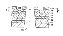
図2Aおよび図2Bは、それぞれ図1のA−A線を通る概略の部分側断面図およびB−B線を通る概略の部分正面断面図である。図2Aおよび図2Bにおいて、基板28の上には薄膜のスタック20が施されている。薄膜のスタック20と基板28とを貫くスロット領域120の区域を、破線で示す。薄膜のスタック20の各層が基板の上にデポジットされるにつれて、スロット領域120は薄膜のスタック20を貫いて延びる。
【0017】
プリントヘッド14の製造工程は、基板28から始まる。1実施形態において、基板28は、当業者に既知の単結晶シリコンウエハーである。直径4インチであれば約525ミクロンの、直径6インチであれば約625ミクロンのウエハーが適当である。1実施形態において、シリコン基板は、約0.55オーム/cmまで低濃度にドープしたp型である。
【0018】
または、出発の基板は、ガラス、半導体材料、金属基複合材料(MMC)、セラミックス基複合材料(CMC)、ポリマー基複合材料(PMC)、またはサンドイッチ状Si/xMcであってもよい。xというフィラー(充填)材料は、真空処理後エッチングによって複合材料から取り除かれる。
【0019】
基板28を、キャッピング層30が覆いシールし、それによって気体および液体バリアー層を提供する。キャッピング層30はバリアー層なので、流体は基板28に流入することができない。キャッピング層30は、二酸化ケイ素、酸化アルミニウム、炭化ケイ素、窒化ケイ素、およびガラス等、様々な異なる材料で形成してもよい。また、キャッピング層30に絶縁誘電材料を用いることも、導電トレースによる相互接続(図示せず)から基板28を絶縁するのに役立つ。キャッピング層30は、スパッタリング、蒸着、およびプラズマ強化化学蒸着(PECVD)等、当業者に既知の様々な方法のうちのいずれを用いて形成してもよい。キャッピング層30の厚さは、基板28を覆いシールするのに十分であれば、いかなる所望の厚さであってもよい。一般的に、キャッピング層30の厚さは、約1から2ミクロンまでである。
【0020】
1実施形態において、キャッピング層は、フィールド酸化物(FOX)30であり、露出した基板28上に熱成長205する。この工程によって、FOXがシリコン基板内に成長するとともに上にデポジットされ、全体で約1.3ミクロンの厚みにわたって形成される。FOX層がシリコンを基板から引っ張るために、FOX層と基板との間には強力な化学結合が確立される。この層は、形成されるMOSFET同士を互いから絶縁し、熱インクジェットのヒータ抵抗器の酸化物下地層の一部として機能する。
【0021】
PECVD技術によって、リンをドープした(n+)二酸化ケイ素の相互誘電性の絶縁ガラス層(PSG)32がデポジットされる。一般的に、PSG層32の厚さは、約1から2ミクロンまでである。1実施形態において、この層は厚さが約0.5ミクロンで、熱インクジェットのヒータ抵抗器の酸化物下地層の残りを形成する。他の実施形態において、厚さの範囲は約0.7から0.9ミクロンである。
【0022】
マスクが施され、PSG層がエッチングされて、MOSFET用の相互接続ビアのための開口部をPSGに設ける。別のマスクが施されエッチングが行われて、ベースのシリコン基板28に接続できるようにする。ビアの形成および使用については、その参照によってその全体が組み込まれる、「Process for Manufacturing Thermal Ink Jet Printhead and Integrated Circuit(IC)Structures Produced Thereby」についてのStoffelへの米国特許番号第4,862,197号(本願の出願人に譲渡されている)において説明されている。
【0023】
この構造の上に抵抗材料でできた層114をデポジットすることによって、発射抵抗器が形成される。1実施形態において、スパッタデポジション技術を用いて、この構造を横切って、タンタルアルミニウムの混合物でできた層114をデポジットする。この混合物の面抵抗は、約30オーム/□(オーム/スクウェア)である。一般的に、抵抗器層114の厚さは約1から2ミクロンまでである。
【0024】
当業者には、タンタルアルミニウム、ニッケルクロム、および窒化チタンを含む様々な好適な抵抗材料が既知である。これらは、任意で酸素、窒素、および炭素等の適当な不純物をドープして、材料の抵抗を調整してもよい。抵抗材料は、スパッタリングや蒸着等、いかなる好適な方法によってデポジットしてもよい。典型的には、抵抗器層は厚さが約100オングストロームから300オングストロームの範囲内である。しかし、厚さがこの範囲外の抵抗器層もまた、本発明の範囲内である。
【0025】
抵抗器層114の上には、導電層115が施される。導電層115は、アルミニウム/銅(4%)、銅、および金を含む様々な異なる材料のうちのいずれで形成してもよく、スパッタリングや蒸着等、いかなる方法によってデポジットしてもよい。一般的に、導電層115の厚さは約1から2ミクロンまでである。1実施形態において、スパッタデポジションを用いて、アルミニウムでできた層115を、約0.5ミクロンの厚さまでデポジットする。
【0026】
抵抗器層114と導電層115とは、フォトリソグラフィー等によってパターニングされ、エッチングされる。図3および図4に示すように、導電層115のうちのある区域がエッチングによって取り除かれて、導電トレース115の下で抵抗器層114から個々の抵抗器134を形成する。1実施形態において、マスクが施されエッチングされて、抵抗器ヒータの幅と導電トレースとを規定する。次に、別のマスクを同様に用いて、ヒータ抵抗器の長さとアルミニウム導線115の末端を規定する。
【0027】
抵抗器および導電トレースの上に、絶縁パッシベーション層117を形成して、導電性の流体を用いた場合の、流体の帯電や装置の腐食を防止する。パッシベーション層117は、二酸化ケイ素、酸化アルミニウム、炭化ケイ素、窒化ケイ素、およびガラス等のいかなる好適な材料で、スパッタリング、蒸着、およびPECVD等のいかなる好適な方法によって、形成してもよい。一般的に、パッシベーション層117の厚さは、約1から2ミクロンまでである。
【0028】
1実施形態において、PECVD法を用いて、構成要素のパッシベーションとして機能する窒化ケイ素/炭化ケイ素の混合物の層117をデポジットする。このパッシベーション層117は、厚さが約0.75ミクロンである。他の実施形態において、厚さは約0.4ミクロンである。この構造の表面には、マスクが施されエッチングされて、金属の相互接続用のビアが作成される。1実施形態において、パッシベーション層117は、圧縮応力下においてこの構造で形成される。
【0029】
パッシベーション層117の上に、キャビテーションバリアー層119が付け加えられる。キャビテーションバリアー層119は、それぞれの噴出される流体滴の後に残る、つぶれていく駆動気泡の力を分散させるのに役立つ。一般的に、キャビテーションバリアー層119の厚さは、約1から2ミクロンまでである。1実施形態において、キャビテーションバリアー層119はタンタルである。タンタル層119は、厚さが約0.6ミクロンであり、パッシベーション、アンチキャビテーション、および接着の層として働く。1実施形態において、キャビテーションバリアー層119は、スロット形成中に基板からエネルギーを吸収して取り去る。タンタルは、ベータ相でデポジットされる、強靱で展性を有する材料である。この材料の結晶粒構造は、この層がまた圧縮応力下での構造をとるようなものになっている。タンタル層は、迅速にスパッタデポジションされ、それによって層内の分子を所定位置に保持する。しかし、タンタル層をアニーリングすると、圧縮応力は開放される。
【0030】
図3に示すように、スロット領域120の区域全般において、基板および薄膜のスタックにドリルスロット122が形成される。ドリルスロット122を形成する方法として、ひとつには、研磨サンドブラストがある。ブラスト装置は、加圧気体(例えば、圧縮空気)源を用いて、薄膜層でコーティングした基板に向かって研磨粒子を噴出して、スロットを形成する。粒子は、気流が高流量(例えば、約2−20グラム/分の流量)で装置から運ぶ。次に粒子はコーティングした基板に接触し、基板を貫いて開口部が形成される。
【0031】
研磨粒子の大きさは、直径が約10−200ミクロンの範囲である。研磨粒子には、例えば、酸化アルミニウム、ガラスビーズ、炭化ケイ素、炭酸水素ナトリウム、ドロマイト、およびウォルナットシェルを含む。
【0032】
1実施形態において、研磨サンドブラストは、スロット領域120に向ける研磨粒子として酸化アルミニウム粒子を用いている。サンドブラストにおいては、約560から610kPaの圧力を用いる。用いるサンドのタイプは、250OPTである。
【0033】
本発明において、金属、プラスチック、ガラス、およびシリコンを含む基板を、貫いてスロットが形成されていてもよい。しかし、本発明は、いかなる特定の基板材料の切断にも限定されるべきではない。同様に、本発明は、いかなる特定の研磨粉の使用にも限定されるべきではない。幅広い様々な異なるシステムおよび粉末を用いることができる。
【0034】
図3に示すように、キャビテーションバリアー層119の上に、ポリマーバリアー層124がデポジットされる。一般的に、バリアー層124の厚さは約20ミクロンまでである。1実施形態において、バリアー層124は、フォトイメージング可能なエポキシ(IBMが開発したSU8等)等の、高速な架橋ポリマーや、信越化学(ShinEtsuTM)が製造したSINR−3010等の、フォトイメージング可能なポリマーまたは感光性シリコーン誘電体から構成されている。
【0035】
他の実施形態において、バリアー層124は、インクの腐食作用に略不活性の有機ポリマープラスチックでできている。この目的に好適なプラスチックポリマーには、例えば、米国デラウェア州ウィルミントン市のデュポン社がVACRELおよびRISTONの商標名で販売している製品がある。バリアー層124の厚さは、約20から30ミクロンである。
【0036】
1実施形態において、スロットのドリリング(穴あけ)の前に、バリアー層124が施されパターニングされる。この実施形態において、図2Bに示すように、ドリルスロット領域120の終わりはキャビテーションバリアー層119である。
【0037】
他の実施形態において、図2Cに示すように、スロット領域120はバリアー層124を貫いて延びる。この実施形態において、研磨サンドブラスト工程は、バリアー層124を貫いて施される。バリアー材料の特性は、スロット形成での棚状部における削りくずの数を減らす助けとなる。ポリマーバリアー材料は、スロット形成中に基板からエネルギーを吸収して取り去り、それによって、基板構造に与える影響を弱める。その結果、基板を貫くクラックの拡大は遅くなり、棚状部における削りくずは減る。
【0038】
1実施形態において、バリアー層124は、本願において説明するように、そこを通って流体が噴出されるオリフィスを含む。他の実施形態において、バリアー層の上にオリフィス層が施され、それによって発射チャンバ132の上にオリフィスが形成される。これについては、以下でより詳細に説明する。
【0039】
図4は、コーティングした基板の平面図であり、図3のC−C線(バリアー層)を通る構造を示す。図4に示すように、基板の形状は通常長方形であり、スロット122は基板内に長さ方向に配置されている。プラスチックバリアー層124は、マスクが施されエッチングされて、棚状部128、流体流チャネル130、および発射チャンバ132を規定する。棚状部128は、スロット122を取り囲んで、チャネル130まで延びている。それぞれの発射チャンバ132は、少なくとも1つの流体チャネル130を有する。バリアー層内の流体チャネル130には、棚状部128に沿って流れる流体の入口がある。図3の矢印で示すように、供給流体(図示せず)は基板28の下にあり、加圧されて、ドリルスロット122を通り発射チャンバ132内へと流れ上がる。図3の矢印で示すように、流体チャネル130は、スロット122から対応する発射チャンバ132に流体を向ける。
【0040】
それぞれの発射チャンバ132内には、加熱要素134がある。加熱要素134は、抵抗材料層114で形成されており、パッシベーション層およびキャビテーションバリアー層でコーティングされている(図3に示す)。加熱要素134を通って電流すなわち「発射信号」が伝わることによって、対応する発射チャンバ内の流体が加熱され、対応するノズルを通って吐出される。
【0041】
加熱要素134と対応する発射チャンバ132とは、スロット122の両側の2つの行に配置され、この2つの行はスロットからの距離が略等しく、それぞれの抵抗器におけるインクチャネル長さが略等しいようになっている。プリントヘッドが1度通過することによって達成される印字スウォースの幅は、抵抗器の各行の長さと略等しく、抵抗器の各行の長さは、スロットの長さと略等しい。
【0042】
本発明の他の実施形態において、マルチスロットのチップと、プリントヘッド14内で互いに隣接するチップとがある。マルチスロットのチップ1つの中での、およびチップ同士の間でのスロット間距離は、スロット形成前に基板をコーティングする本発明を用いて、棚状部における削りくずの大きさおよび数を低減することによって、約20%までの割合だけ小さくなる。ドリルの歩留まり(ドリリング後に仕様書の範囲内におさまるチップの数)は、本発明の方法を用いて約25−27%までの割合だけ上昇する。削りくずの歩留まりロス(削りくずによる歩留まりロス)もまた、約30%までの割合だけ低下する。ドリル歩留まりと削りくずの歩留まりロスとに高い相関関係があるのは、削りくずが歩留まりロスの最も大きい要因であるという事実による。
【0043】
パターニングしたFOX層、PSG層、およびパッシベーション層が基板上にデポジットされた第1の実施形態において、スロット歩留まりは約83%であった。パターニングしたFOX層、PSG層、パッシベーション層、およびタンタル層が基板上にデポジットされた第2の実施形態において、スロット歩留まりは約87%であった。第1の実施形態と第2の実施形態との間の割合の差は、95%の確かさのレベルで統計的に有意である。パターニングしないFOX層、PSG層、パッシベーション層、TaAl/Al層、およびタンタル層が基板上にデポジットされた第3の実施形態において、スロット歩留まりは約88%であった。
【0044】
本発明において、ドリリング前に基板上に薄膜層を施すことによって、削りくずの数が約90%までの割合だけ減る。1実施形態において、長さがスロット幅の約1/4よりも長い削りくずの数は、約40個以下である。(スロット幅は、典型的には約150から200ミクロンである。1実施形態において、スロット幅は約170ミクロンであり、カウントされる削りくずの長さは約40ミクロンである。)他の実施形態において、削りくずの数は、約10個以下である。特に、FOX、パッシベーション、アルミニウム、タンタルアルミニウム、およびタンタルがシリコン基板上にデポジットされる1実施形態において、削りくずの数は、約10個から約30個の間である。
【0045】
本発明の原理、好ましい実施形態、および実施例を上で説明した。しかし、本発明は、説明した特定の実施形態に限定されるものとして解釈されるべきではない。例えば、プリントヘッドを形成する他の実施形態において基板の上に施される、ゲート酸化物(GOX)層、金、バリアー材料用に用いるポリマー層、および多結晶シリコン等の層が、基板の上にデポジットされてもよい。
【0046】
1実施形態において、基板の上には1つの層が施される。または、基板の上には1つよりも多い層が施される。さらに、本発明は、説明した各層の順番に限定されるものではない。本発明は、上述の各層をいかなる順番で配置することも含む。特に、基板の上に以下の各層のうちの1つまたはそれよりも多くを施してもよい。すなわち、次のいかなる組み合わせでもよい、展性を有する材料の層、金属、圧縮応力下にある材料、抵抗材料(タンタルアルミニウム等)、導電材料(アルミニウム等)、キャビテーションバリアー層(タンタル等)、パッシベーション層(窒化ケイ素や炭化ケイ素等)、基板から成長した絶縁層(FOX等)、PSG、ポリマー層、および誘電層。
【0047】
1実施形態において、スロット領域の上の薄膜のスタックの厚さは、0.25ミクロンから約50ミクロンまでの範囲である。他の実施形態において、膜の厚さは少なくとも約21/2ミクロンである。他の実施形態において、膜の厚さは少なくとも約3ミクロンである。
【0048】
さらに、基板のスロットは、ダイヤモンドソーによる切断等、他の機械的方法によって形成してもよく、レーザー切断/アブレーションによって形成してもよい。したがって、上述の実施形態は、限定的ではなく例示的であるとみなすべきであり、特許請求項の範囲によって規定される本発明の範囲から逸脱することなく当業者がそのような実施形態において変形を行ってもよい、ということが理解されるべきである。
【0049】
上記の実施形態は、以下の発明を含んでいる。
【0050】
1. スロット122を取り囲む棚状部(128)における削りくずの数を最小にしながらスロットをつけた基板(28)を形成する方法であって、基板(28)の上に薄膜(20、30、32、114、115、117、119および/または124)をデポジットする段階と、前記基板(28)と前記薄膜(20、30、32、114、115、117、119および/または124)とを貫いて延びるスロット領域(120)を貫いて前記基板(28)に前記スロット(122)を形成する段階とを含む方法。
【0051】
2. 前記薄膜は金属膜(114、115および/または119)である、前記1に記載の方法。
【0052】
3. 前記薄膜はポリマー膜(124)である、前記1に記載の方法。
【0053】
4. 薄膜は誘電膜(30、32、および/または124)である、前記1に記載の方法。
【0054】
5. 前記薄膜は展性を有する材料である、前記1に記載の方法。
【0055】
6. 前記デポジットされる薄膜は圧縮応力を受ける、前記1に記載の方法。
【0056】
7. スロット(122)を取り囲む棚状部(128)におけるクラック形成を最小にしながらスロットをつけた基板(28)を形成する方法であって、基板(28)の上に薄膜(20、30、32、114、115、117、119および/または124)をデポジットする段階と、前記基板(28)と前記薄膜とを貫いて延びるスロット領域(120)を貫いて前記基板(28)に前記スロット(122)を形成する段階とを含む方法。
【0057】
8. 基板(28)にスロット(122)を形成する方法であって、基板(28)の上に展性を有する薄膜(20、30、32、114、115、117、119および/または124)をデポジットする段階と、前記基板(28)と前記展性を有する薄膜とを貫いて延びるスロット領域(120)を貫いて前記基板(28)にスロット(122)を形成する段階とを含む方法。
【0058】
9. 前記薄膜は圧縮応力を受けた状態でデポジットされる、前記8に記載の方法。
【0059】
10. 中央供給プリントヘッド(14)用のコーティングした基板(28)であって、基板(28)と、該基板(28)の上に施されるポリマー膜(124)と、前記基板(28)と前記ポリマー膜(124)とを貫いて延びる、スロット領域(120)とを含む、コーティングした基板。
【0060】
11. 中央供給プリントヘッド(14)用のコーティングした基板(28)であって、基板(28)と、該基板(28)の上に施される金属膜(114、115および/または119)と、前記基板(28)と前記金属膜(114、115および/または119)とを貫いて延びる、スロット領域(120)とを含む、コーティングした基板。
【0061】
12. 前記金属膜(114、115および/または119)は圧縮応力を受けた状態にある、前記11に記載の基板(28)。
【0062】
13. 中央供給プリントヘッド(14)用のコーティングした基板(28)であって、基板(28)と、該基板(28)の上に施される膜(30、32、114、115、117、119および/または124)であって、厚さが少なくとも約2.5ミクロンである膜と、前記基板(28)と前記膜とを貫いて延びる、スロット領域(120)とを含む、コーティングした基板。
【0063】
14. 中央供給プリントヘッド(14)であって、基板(28)と、該基板(28)の上に施される金属膜(114、115および/または119)と、前記基板(28)と前記金属膜(114、115および/または119)とを貫いて延びる、スロット領域(120)とを含む、中央供給プリントヘッド。
【図面の簡単な説明】
【図1】 本発明のプリントヘッドを有するインクジェットカートリッジの図である。
【図2】 本発明の薄膜のスタックを示す図である。(A)は基板の上に薄膜コーティングを施した状態の、図1のA−A線を通る概略側断面図である。(B)は薄膜コーティングおよび基板の、図1のB−B線を通る概略正面断面図である。(C)はバリアー層をその上に施した状態の、図2Bの構造図である。
【図3】 スロット領域を取り除いた状態の、図2Bの構造図である。
【図4】 図3の構造のC−C線を通る図である。
【符号の説明】
14 中央供給プリントヘッド
28 基板
30キャッピング層
32 絶縁ガラス層
114抵抗器層
115導電層
119 キャビテーションバリアー層
120 スロット領域
122 スロット
124 ポリマーバリアー膜
128 棚状部[0001]
BACKGROUND OF THE INVENTION
The present invention relates to substrates such as those used in ink jet print heads and the like. In particular, the substrate is coated with at least one thin film layer and a slot region extends through the substrate and the thin film layer.
[0002]
[Prior art]
Various ink jet printing devices are known in the art, including both thermally actuated print heads and mechanically actuated print heads. A thermally actuated print head uses a resistive element or the like to eject ink, and a mechanically actuated print head uses a piezoelectric transducer or the like.
[0003]
A typical thermal ink jet printhead has a plurality of thin film resistors provided on a semiconductor substrate. On the substrate, a nozzle plate and a barrier layer are provided to define a firing chamber near each resistor. By passing a current or “fire signal” through the resistor, the ink in the corresponding firing chamber is heated and ejected through the corresponding nozzle.
[0004]
Ink is typically delivered to the firing chamber through a supply slot machined into the semiconductor substrate. The shape of the substrate is usually rectangular, and the slots are arranged in the length direction in the substrate. The resistors are typically arranged in two rows on either side of the slot, and preferably the two rows are approximately equal in distance from the slot so that the ink channel length in each resistor is approximately equal. ing. The width of the print swath achieved by a single pass of the print head is approximately equal to the length of each row of resistors, and the length of each row of resistors is approximately equal to the length of the slot.
[0005]
The supply slot is typically formed by sand drilling (also known as “sand slotting”). This method is a fast, relatively simple and scalable process. In the sandblasting method, the opening can be formed in the substrate with high accuracy, and substantial damage to surrounding components and materials is generally avoided. Also, the openings can be formed by cutting many different types of substrates without generating excessive heat. Furthermore, the relative placement accuracy during the manufacturing process can be improved.
[0006]
Sand slotting provides such obvious advantages, but it is also disadvantageous in that microcracks can occur in the semiconductor substrate. Such microcracks significantly lower the breaking strength of the substrate, and as a result, cracks occur in the chip, resulting in a considerable yield loss. Also, if the breaking strength is low, the length of the substrate is limited, which in turn affects the height of the print swath and the overall print speed.
[0007]
[Problems to be solved by the invention]
In addition, sand slotting typically creates shavings on the substrate on both the input and output sides of the slot. Such shavings create two distinct problems. The shavings are typically tens of microns in size, limiting how close the firing chamber can be placed to the edge of the slot. Sometimes the shavings are larger than this, resulting in yield loss in the manufacturing process. This shaving problem becomes more frequent as the desired slot length increases and the desired slot width decreases.
[0008]
[Means for Solving the Problems]
In the present invention, a coated substrate for a central feed printhead has a substrate, a thin film applied over the substrate, and a slot region extending through the substrate and the thin film. In one embodiment, a plurality of thin films, or stacks of thin films, are deposited on a substrate. In this embodiment, the slot region extends through the plurality of thin films.
[0009]
A slot is formed through the substrate and the slot region of the thin film. The thin film applied on the substrate minimizes the number of shavings in the shelf surrounding the slot and the formation of cracks through the substrate. In one embodiment, the slot is mechanically formed.
[0010]
In one embodiment, the thin film is at least one of a metal film, a polymer film, and a dielectric film. In other embodiments, the thin film material is malleable and / or deposited under compression.
[0011]
In one embodiment, the substrate is silicon and the thin film is an insulating layer grown from the substrate, such as a field oxide. In one embodiment, the thin film is PSG. In one embodiment, the thin film is a passivation layer, such as at least one of silicon nitride and silicon carbide. In one embodiment, the thin film is a cavitation barrier layer such as tantalum. In the present invention, any combination of thin films may be applied on the substrate.
[0012]
The minimum thickness of each thin film layer is about 0.25 microns. In one embodiment where there are multiple thin films coated on a substrate, the thickness of the thin film is up to about 50 microns, depending on the material and thickness of the individual layers. In one embodiment, the thickness of the thin film stack is at least about 2.5 microns.
[0013]
DETAILED DESCRIPTION OF THE INVENTION
By coating a material such as metal, dielectric, polymer, etc. on the substrate, the chips on the substrate resulting from the slot formation are reduced in size and number. In general, the number of layers and the thickness of each layer are directly correlated to the reduction in the size and number of shavings. In other embodiments, malleable or non-brittle materials are used with the present invention that can be greatly deformed prior to failure. In yet other embodiments, the layer coating the substrate places this structure under compressive stress. This compressive stress opposes the tension experienced by the coated substrate structure during slot formation.
[0014]
As described in more detail below, in general, the number of layers deposited on the substrate, the thickness of each deposited layer, the amount of compressive stress in each layer, and the malleability of the material in each layer, respectively, There is a direct correlation in reducing the number of shavings on the chip shelf.
[0015]
FIG. 1 is a perspective view of an
[0016]
2A and 2B are a schematic partial side sectional view through line AA in FIG. 1 and a schematic partial front sectional view through line BB, respectively. 2A and 2B, a
[0017]
The manufacturing process of the
[0018]
Alternatively, the starting substrate may be glass, semiconductor material, metal matrix composite (MMC), ceramic matrix composite (CMC), polymer matrix composite (PMC), or sandwich Si / xMc. The filler material x is removed from the composite by etching after vacuum processing.
[0019]
[0020]
In one embodiment, the capping layer is field oxide (FOX) 30 and is thermally grown 205 on the exposed
[0021]
PECVD technology deposits a phosphorus-doped (n +) silicon dioxide interdielectric insulating glass layer (PSG) 32. Generally, the thickness of the
[0022]
A mask is applied and the PSG layer is etched to provide openings in the PSG for interconnect vias for the MOSFET. Another mask is applied and etched to allow connection to the
[0023]
A firing resistor is formed by depositing a
[0024]
Those skilled in the art are aware of various suitable resistive materials including tantalum aluminum, nickel chromium, and titanium nitride. These may optionally be doped with suitable impurities such as oxygen, nitrogen, and carbon to adjust the resistance of the material. The resistive material may be deposited by any suitable method such as sputtering or evaporation. Typically, the resistor layer has a thickness in the range of about 100 angstroms to 300 angstroms. However, resistor layers with thicknesses outside this range are also within the scope of the present invention.
[0025]
A
[0026]
The
[0027]
An insulating
[0028]
In one embodiment, a PECVD process is used to deposit a
[0029]
On top of the
[0030]
As shown in FIG. 3,
[0031]
The size of the abrasive particles is in the range of about 10-200 microns in diameter. Abrasive particles include, for example, aluminum oxide, glass beads, silicon carbide, sodium bicarbonate, dolomite, and walnut shell.
[0032]
In one embodiment, the abrasive sandblast uses aluminum oxide particles as abrasive particles directed toward the
[0033]
In the present invention, a slot may be formed through a substrate including metal, plastic, glass, and silicon. However, the present invention should not be limited to cutting any particular substrate material. Similarly, the present invention should not be limited to the use of any particular abrasive powder. A wide variety of different systems and powders can be used.
[0034]
As shown in FIG. 3, a
[0035]
In other embodiments, the
[0036]
In one embodiment, a
[0037]
In other embodiments, the
[0038]
In one embodiment, the
[0039]
FIG. 4 is a plan view of the coated substrate, showing a structure passing through the CC line (barrier layer) of FIG. As shown in FIG. 4, the shape of the substrate is usually rectangular, and the
[0040]
Within each firing
[0041]
The
[0042]
In other embodiments of the present invention, there are multi-slot chips and chips that are adjacent to each other in the
[0043]
In the first embodiment in which the patterned FOX layer, PSG layer, and passivation layer were deposited on the substrate, the slot yield was about 83%. In the second embodiment in which the patterned FOX layer, PSG layer, passivation layer, and tantalum layer were deposited on the substrate, the slot yield was about 87%. The difference in proportion between the first and second embodiments is statistically significant at the 95% certainty level. In the third embodiment in which the unpatterned FOX layer, PSG layer, passivation layer, TaAl / Al layer, and tantalum layer were deposited on the substrate, the slot yield was about 88%.
[0044]
In the present invention, by applying the thin film layer on the substrate before drilling, the number of shavings is reduced by up to about 90%. In one embodiment, the number of shavings whose length is greater than about 1/4 of the slot width is about 40 or less. (The slot width is typically about 150 to 200 microns. In one embodiment, the slot width is about 170 microns and the length of the counted chip is about 40 microns.) Other implementations In the form, the number of shavings is about 10 or less. In particular, in one embodiment where FOX, passivation, aluminum, tantalum aluminum, and tantalum are deposited on a silicon substrate, the number of shavings is between about 10 and about 30.
[0045]
The principles, preferred embodiments, and examples of the present invention have been described above. However, this invention should not be construed as limited to the particular embodiments described. For example, layers such as a gate oxide (GOX) layer, gold, a polymer layer used for barrier materials, and polycrystalline silicon applied on the substrate in other embodiments forming a printhead are formed on the substrate. May be deposited.
[0046]
In one embodiment, a layer is applied over the substrate. Alternatively, more than one layer is applied on the substrate. Further, the present invention is not limited to the order of each layer described. The present invention includes arranging the above-mentioned layers in any order. In particular, one or more of the following layers may be applied on the substrate. That is, any combination of the following: malleable material layer, metal, material under compressive stress, resistance material (tantalum aluminum, etc.), conductive material (aluminum, etc.), cavitation barrier layer (tantalum, etc.), passivation Layers (such as silicon nitride and silicon carbide), insulating layers (such as FOX) grown from the substrate, PSG, polymer layers, and dielectric layers.
[0047]
In one embodiment, the thickness of the stack of thin films above the slot region ranges from 0.25 microns to about 50 microns. In other embodiments, the thickness of the membrane is at least about 2 1 / 2 Micron. In other embodiments, the thickness of the membrane is at least about 3 microns.
[0048]
Furthermore, the slot of the substrate may be formed by other mechanical methods such as cutting with a diamond saw, or may be formed by laser cutting / ablation. Accordingly, the above embodiments are to be regarded as illustrative rather than restrictive and modifications can be made in such embodiments by those skilled in the art without departing from the scope of the invention as defined by the scope of the claims. It should be understood that may be performed.
[0049]
The above embodiments include the following inventions.
[0050]
1. A method of forming a slotted substrate (28) while minimizing the number of shavings in a shelf (128) surrounding a
[0051]
2. The method of claim 1, wherein the thin film is a metal film (114, 115 and / or 119).
[0052]
3. The method of claim 1, wherein the thin film is a polymer film (124).
[0053]
4). The method of claim 1, wherein the thin film is a dielectric film (30, 32, and / or 124).
[0054]
5. 2. The method according to 1 above, wherein the thin film is a malleable material.
[0055]
6). The method of claim 1, wherein the deposited thin film is subjected to compressive stress.
[0056]
7). A method of forming a slotted substrate (28) while minimizing crack formation in a shelf (128) surrounding the slot (122), comprising a thin film (20, 30, 32, 114, 115, 117, 119 and / or 124) and slot (122) in the substrate (28) through a slot region (120) extending through the substrate (28) and the thin film. Forming a method.
[0057]
8). A method of forming a slot (122) in a substrate (28), wherein a malleable thin film (20, 30, 32, 114, 115, 117, 119 and / or 124) is deposited on the substrate (28). And forming slots (122) in the substrate (28) through slot regions (120) extending through the substrate (28) and the malleable thin film.
[0058]
9. 9. The method of claim 8, wherein the thin film is deposited under a compressive stress.
[0059]
10. A coated substrate (28) for a central feed printhead (14) comprising a substrate (28), a polymer film (124) applied over the substrate (28), the substrate (28) and the substrate A coated substrate comprising a slot region (120) extending through the polymer membrane (124).
[0060]
11. A coated substrate (28) for a central feed printhead (14), the substrate (28) and a metal film (114, 115 and / or 119) applied over the substrate (28); A coated substrate comprising a substrate (28) and a slot region (120) extending through said metal film (114, 115 and / or 119).
[0061]
12 The substrate (28) of claim 11, wherein the metal film (114, 115 and / or 119) is under a compressive stress.
[0062]
13. A coated substrate (28) for a central feed printhead (14) comprising a substrate (28) and a film (30, 32, 114, 115, 117, 119) applied on the substrate (28). 124) a coated substrate comprising a membrane having a thickness of at least about 2.5 microns and a slot region (120) extending through the substrate (28) and the membrane.
[0063]
14 A central supply printhead (14) comprising a substrate (28), a metal film (114, 115 and / or 119) applied over the substrate (28), the substrate (28) and the metal film A centrally-fed printhead including a slot region (120) extending through (114, 115 and / or 119).
[Brief description of the drawings]
FIG. 1 is a diagram of an ink jet cartridge having a print head of the present invention.
FIG. 2 shows a stack of thin films of the present invention. (A) is a schematic sectional side view through the AA line of FIG. 1 in the state which gave the thin film coating on the board | substrate. (B) is a schematic front sectional view of the thin film coating and substrate taken along line BB in FIG. FIG. 2C is a structural diagram of FIG. 2B with a barrier layer applied thereon.
FIG. 3 is a structural diagram of FIG. 2B with the slot region removed.
4 is a view taken along line CC of the structure of FIG. 3;
[Explanation of symbols]
14 Central supply print head
28 substrates
30 capping layers
32 Insulating glass layer
114 resistor layer
115 conductive layer
119 Cavitation barrier layer
120 slot area
122 slots
124 Polymer barrier membrane
128 shelf
Claims (11)
基板上に第1の層として絶縁誘電バリアー薄膜層を堆積すること、
前記第1の層上に第2の層として層間の誘電薄膜層を堆積すること、
前記第2の層上に第3の層として抵抗薄膜層を堆積すること、
前記第3の層上に第4の層として金属の導電性薄膜層を堆積すること、および
前記複数の薄膜層および前記基板を貫いて、スロット領域により画定されるスロットを形成して延ばすことであって、それにより、スロットを取り囲む棚状部における削りくずの数を最小にするようなスロットを形成して延ばすこと、を含み、
前記絶縁誘電バリアー薄膜層と前記層間の誘電薄膜層の少なくとも一つが圧縮応力下にあることを特徴とする方法。A method of forming a slotted substrate,
Depositing an insulating dielectric barrier thin film layer as a first layer on a substrate;
Depositing an interlayer dielectric thin film layer as a second layer on the first layer;
Depositing a resistive thin film layer as a third layer on the second layer;
Depositing a metal conductive thin film layer as a fourth layer on the third layer, and extending through the plurality of thin film layers and the substrate to form a slot defined by a slot region. Forming and extending a slot so as to minimize the number of shavings in the shelf surrounding the slot,
A method wherein at least one of the insulating dielectric barrier thin film layer and the dielectric thin film layer between the layers is under compressive stress.
基板と、
該基板上に付着される薄膜であって、少なくとも絶縁誘電バリアー層、層間の誘電薄膜層、抵抗層、および金属導電層からなる複数の層を含む、薄膜と、
前記基板および前記薄膜を貫いて延びるスロット領域であって、前記複数の層が前記基板上に所定の順序で堆積されることにより、スロットが該スロット領域を貫いて前記基板に形成される場合、該スロット領域を取り囲む棚状部における削りくずの数が最小になる、スロット領域と、
を備え、
前記絶縁誘電バリアー層と前記層間の誘電薄膜層のうちの少なくとも一つが圧縮応力下にあることを特徴とするコーティングした基板。A coated substrate for a central feed printhead,
A substrate,
A thin film deposited on the substrate, comprising a plurality of layers comprising at least an insulating dielectric barrier layer, an interlayer dielectric thin film layer, a resistance layer, and a metal conductive layer;
A slot region extending through the substrate and the thin film, wherein the plurality of layers are deposited on the substrate in a predetermined order such that a slot is formed in the substrate through the slot region; A slot area in which the number of shavings in the shelf surrounding the slot area is minimized; and
With
A coated substrate , wherein at least one of the insulating dielectric barrier layer and the dielectric thin film layer between the layers is under compressive stress.
Applications Claiming Priority (2)
| Application Number | Priority Date | Filing Date | Title |
|---|---|---|---|
| US09/772752 | 2001-01-30 | ||
| US09/772,752 US6648732B2 (en) | 2001-01-30 | 2001-01-30 | Thin film coating of a slotted substrate and techniques for forming slotted substrates |
Publications (3)
| Publication Number | Publication Date |
|---|---|
| JP2002248777A JP2002248777A (en) | 2002-09-03 |
| JP2002248777A5 JP2002248777A5 (en) | 2005-04-07 |
| JP4166476B2 true JP4166476B2 (en) | 2008-10-15 |
Family
ID=25096103
Family Applications (1)
| Application Number | Title | Priority Date | Filing Date |
|---|---|---|---|
| JP2002011197A Expired - Fee Related JP4166476B2 (en) | 2001-01-30 | 2002-01-21 | Formation technology of substrate with slot |
Country Status (4)
| Country | Link |
|---|---|
| US (2) | US6648732B2 (en) |
| EP (2) | EP2000309A3 (en) |
| JP (1) | JP4166476B2 (en) |
| DE (1) | DE60229316D1 (en) |
Families Citing this family (11)
| Publication number | Priority date | Publication date | Assignee | Title |
|---|---|---|---|---|
| KR100335311B1 (en) * | 1994-09-13 | 2002-11-14 | 주식회사 디피아이 | Paint composition containing gas-checking resistant acryl resin composition |
| US6648732B2 (en) * | 2001-01-30 | 2003-11-18 | Hewlett-Packard Development Company, L.P. | Thin film coating of a slotted substrate and techniques for forming slotted substrates |
| JP2004130579A (en) * | 2002-10-09 | 2004-04-30 | Sony Corp | Liquid discharge head, liquid discharge device, and manufacturing method for liquid discharge head |
| JP2004230770A (en) * | 2003-01-31 | 2004-08-19 | Fuji Photo Film Co Ltd | Inkjet head |
| US7594328B2 (en) * | 2003-10-03 | 2009-09-29 | Hewlett-Packard Development Company, L.P. | Method of forming a slotted substrate with partially patterned layers |
| US7784916B2 (en) * | 2006-09-28 | 2010-08-31 | Lexmark International, Inc. | Micro-fluid ejection heads with multiple glass layers |
| BRPI1011559B1 (en) * | 2009-06-29 | 2020-01-07 | Videojet Technologies Inc. | INK JET PRINTING SYSTEM AND METHOD FOR PREPARING A PRINTING HEAD SYSTEM |
| US8382253B1 (en) | 2011-08-25 | 2013-02-26 | Hewlett-Packard Development Company, L.P. | Fluid ejection device and methods of fabrication |
| US8727499B2 (en) | 2011-12-21 | 2014-05-20 | Hewlett-Packard Development Company, L.P. | Protecting a fluid ejection device resistor |
| US9016836B2 (en) | 2013-05-14 | 2015-04-28 | Stmicroelectronics, Inc. | Ink jet printhead with polarity-changing driver for thermal resistors |
| US9016837B2 (en) | 2013-05-14 | 2015-04-28 | Stmicroelectronics, Inc. | Ink jet printhead device with compressive stressed dielectric layer |
Family Cites Families (18)
| Publication number | Priority date | Publication date | Assignee | Title |
|---|---|---|---|---|
| US2989046A (en) * | 1958-06-05 | 1961-06-20 | Paramount Pictures Corp | Method for drilling finished holes in glass |
| DE2604939C3 (en) | 1976-02-09 | 1978-07-27 | Ibm Deutschland Gmbh, 7000 Stuttgart | Method for producing at least one through hole, in particular a nozzle for inkjet printers |
| US4239954A (en) * | 1978-12-11 | 1980-12-16 | United Technologies Corporation | Backer for electron beam hole drilling |
| US4894664A (en) | 1986-04-28 | 1990-01-16 | Hewlett-Packard Company | Monolithic thermal ink jet printhead with integral nozzle and ink feed |
| US4862197A (en) | 1986-08-28 | 1989-08-29 | Hewlett-Packard Co. | Process for manufacturing thermal ink jet printhead and integrated circuit (IC) structures produced thereby |
| IT1234800B (en) * | 1989-06-08 | 1992-05-27 | C Olivetti & C Spa Sede Via Je | MANUFACTURING PROCEDURE OF INK-JET THERMAL HEADS AND HEADS SO OBTAINED |
| GB2241186A (en) | 1990-02-24 | 1991-08-28 | Rolls Royce Plc | Anti-sputtercoating |
| US5105588A (en) * | 1990-09-10 | 1992-04-21 | Hewlett-Packard Company | Method and apparatus for simultaneously forming a plurality of openings through a substrate |
| US5703631A (en) | 1992-05-05 | 1997-12-30 | Compaq Computer Corporation | Method of forming an orifice array for a high density ink jet printhead |
| JP3196796B2 (en) | 1992-06-24 | 2001-08-06 | セイコーエプソン株式会社 | Nozzle forming method for inkjet recording head |
| US5308442A (en) | 1993-01-25 | 1994-05-03 | Hewlett-Packard Company | Anisotropically etched ink fill slots in silicon |
| BE1007894A3 (en) * | 1993-12-20 | 1995-11-14 | Philips Electronics Nv | Method for manufacturing a plate of non-metallic materials with a pattern of holes and / or cavities. |
| JPH08267753A (en) * | 1995-03-29 | 1996-10-15 | Brother Ind Ltd | Manufacture of nozzle |
| US5658471A (en) | 1995-09-22 | 1997-08-19 | Lexmark International, Inc. | Fabrication of thermal ink-jet feed slots in a silicon substrate |
| KR100311880B1 (en) | 1996-11-11 | 2001-12-20 | 미다라이 후지오 | Method of producing a through-hole, silicon substrate having a through-hole, device using such a substrate, method of producing an ink-jet print head, and ink-jet print head |
| US6238269B1 (en) * | 2000-01-26 | 2001-05-29 | Hewlett-Packard Company | Ink feed slot formation in ink-jet printheads |
| FR2811588B1 (en) * | 2000-07-13 | 2002-10-11 | Centre Nat Rech Scient | THERMAL INJECTION AND DOSING HEAD, MANUFACTURING METHOD THEREOF, AND FUNCTIONALIZATION OR ADDRESSING SYSTEM COMPRISING THE SAME |
| US6648732B2 (en) * | 2001-01-30 | 2003-11-18 | Hewlett-Packard Development Company, L.P. | Thin film coating of a slotted substrate and techniques for forming slotted substrates |
-
2001
- 2001-01-30 US US09/772,752 patent/US6648732B2/en not_active Expired - Fee Related
-
2002
- 2002-01-21 EP EP08075640A patent/EP2000309A3/en not_active Withdrawn
- 2002-01-21 EP EP02250377A patent/EP1226947B1/en not_active Expired - Lifetime
- 2002-01-21 DE DE60229316T patent/DE60229316D1/en not_active Expired - Lifetime
- 2002-01-21 JP JP2002011197A patent/JP4166476B2/en not_active Expired - Fee Related
-
2003
- 2003-10-03 US US10/679,097 patent/US6945634B2/en not_active Expired - Fee Related
Also Published As
| Publication number | Publication date |
|---|---|
| EP2000309A3 (en) | 2009-12-16 |
| EP1226947A1 (en) | 2002-07-31 |
| EP2000309A2 (en) | 2008-12-10 |
| US6648732B2 (en) | 2003-11-18 |
| DE60229316D1 (en) | 2008-11-27 |
| US20020102918A1 (en) | 2002-08-01 |
| US20040067319A1 (en) | 2004-04-08 |
| EP1226947B1 (en) | 2008-10-15 |
| JP2002248777A (en) | 2002-09-03 |
| US6945634B2 (en) | 2005-09-20 |
Similar Documents
| Publication | Publication Date | Title |
|---|---|---|
| US7716832B2 (en) | Method of manufacturing a fluid ejection device | |
| US4951063A (en) | Heating elements for thermal ink jet devices | |
| JP4166476B2 (en) | Formation technology of substrate with slot | |
| US20100321447A1 (en) | Protective layers for micro-fluid ejection devices and methods for depositing same | |
| US6786575B2 (en) | Ink jet heater chip and method therefor | |
| JP3408292B2 (en) | Print head | |
| US7198358B2 (en) | Heating element, fluid heating device, inkjet printhead, and print cartridge having the same and method of making the same | |
| US6929349B2 (en) | Thin film ink jet printhead adhesion enhancement | |
| EP1270233B1 (en) | Slotted substrate and slotting process | |
| US20030098900A1 (en) | Ink-jet head, and method for manufacturing the same | |
| US7594328B2 (en) | Method of forming a slotted substrate with partially patterned layers | |
| KR100553912B1 (en) | Inkjet printhead and method for manufacturing the same | |
| JP2008149666A (en) | Inkjet recording head | |
| WO2009005489A1 (en) | Protective layers for micro-fluid ejection devices | |
| JPH07125210A (en) | Thermal ink jet head | |
| JPH07125206A (en) | Thermal ink jet head | |
| JP2007276150A (en) | Inkjet recording head and method for manufacturing inkjet recording head | |
| JPH10181019A (en) | Liquid-jet recording head | |
| JPH06305145A (en) | Thermal ink jet head | |
| JP2003226021A (en) | Inkjet head and method of manufacturing inkjet head | |
| JPH06320730A (en) | Thermal ink jet head | |
| JPH05330047A (en) | Substrate for ink-jet recording head, ink-jet recording head and ink-jet recording device | |
| JPH05293966A (en) | Production of thermal ink jet head chip | |
| JP2006224591A (en) | Method for manufacturing inkjet recording head |
Legal Events
| Date | Code | Title | Description |
|---|---|---|---|
| A521 | Written amendment |
Free format text: JAPANESE INTERMEDIATE CODE: A523 Effective date: 20040527 |
|
| A621 | Written request for application examination |
Free format text: JAPANESE INTERMEDIATE CODE: A621 Effective date: 20040527 |
|
| A977 | Report on retrieval |
Free format text: JAPANESE INTERMEDIATE CODE: A971007 Effective date: 20070824 |
|
| A131 | Notification of reasons for refusal |
Free format text: JAPANESE INTERMEDIATE CODE: A131 Effective date: 20070911 |
|
| A601 | Written request for extension of time |
Free format text: JAPANESE INTERMEDIATE CODE: A601 Effective date: 20071210 |
|
| A602 | Written permission of extension of time |
Free format text: JAPANESE INTERMEDIATE CODE: A602 Effective date: 20071213 |
|
| A521 | Written amendment |
Free format text: JAPANESE INTERMEDIATE CODE: A523 Effective date: 20080109 |
|
| A02 | Decision of refusal |
Free format text: JAPANESE INTERMEDIATE CODE: A02 Effective date: 20080205 |
|
| A521 | Written amendment |
Free format text: JAPANESE INTERMEDIATE CODE: A523 Effective date: 20080604 |
|
| A911 | Transfer to examiner for re-examination before appeal (zenchi) |
Free format text: JAPANESE INTERMEDIATE CODE: A911 Effective date: 20080612 |
|
| TRDD | Decision of grant or rejection written | ||
| A01 | Written decision to grant a patent or to grant a registration (utility model) |
Free format text: JAPANESE INTERMEDIATE CODE: A01 Effective date: 20080701 |
|
| A01 | Written decision to grant a patent or to grant a registration (utility model) |
Free format text: JAPANESE INTERMEDIATE CODE: A01 |
|
| A61 | First payment of annual fees (during grant procedure) |
Free format text: JAPANESE INTERMEDIATE CODE: A61 Effective date: 20080730 |
|
| R150 | Certificate of patent or registration of utility model |
Free format text: JAPANESE INTERMEDIATE CODE: R150 |
|
| FPAY | Renewal fee payment (event date is renewal date of database) |
Free format text: PAYMENT UNTIL: 20110808 Year of fee payment: 3 |
|
| LAPS | Cancellation because of no payment of annual fees |