JP4140214B2 - Capacitor manufacturing method for nonvolatile semiconductor memory device - Google Patents
Capacitor manufacturing method for nonvolatile semiconductor memory device Download PDFInfo
- Publication number
- JP4140214B2 JP4140214B2 JP2001189273A JP2001189273A JP4140214B2 JP 4140214 B2 JP4140214 B2 JP 4140214B2 JP 2001189273 A JP2001189273 A JP 2001189273A JP 2001189273 A JP2001189273 A JP 2001189273A JP 4140214 B2 JP4140214 B2 JP 4140214B2
- Authority
- JP
- Japan
- Prior art keywords
- capacitor
- film
- manufacturing
- nonvolatile semiconductor
- semiconductor memory
- Prior art date
- Legal status (The legal status is an assumption and is not a legal conclusion. Google has not performed a legal analysis and makes no representation as to the accuracy of the status listed.)
- Expired - Fee Related
Links
Images


Classifications
-
- H—ELECTRICITY
- H10—SEMICONDUCTOR DEVICES; ELECTRIC SOLID-STATE DEVICES NOT OTHERWISE PROVIDED FOR
- H10B—ELECTRONIC MEMORY DEVICES
- H10B99/00—Subject matter not provided for in other groups of this subclass
-
- H—ELECTRICITY
- H01—ELECTRIC ELEMENTS
- H01L—SEMICONDUCTOR DEVICES NOT COVERED BY CLASS H10
- H01L28/00—Passive two-terminal components without a potential-jump or surface barrier for integrated circuits; Details thereof; Multistep manufacturing processes therefor
- H01L28/40—Capacitors
- H01L28/55—Capacitors with a dielectric comprising a perovskite structure material
-
- H—ELECTRICITY
- H01—ELECTRIC ELEMENTS
- H01L—SEMICONDUCTOR DEVICES NOT COVERED BY CLASS H10
- H01L28/00—Passive two-terminal components without a potential-jump or surface barrier for integrated circuits; Details thereof; Multistep manufacturing processes therefor
- H01L28/40—Capacitors
- H01L28/60—Electrodes
- H01L28/75—Electrodes comprising two or more layers, e.g. comprising a barrier layer and a metal layer
-
- H—ELECTRICITY
- H10—SEMICONDUCTOR DEVICES; ELECTRIC SOLID-STATE DEVICES NOT OTHERWISE PROVIDED FOR
- H10B—ELECTRONIC MEMORY DEVICES
- H10B53/00—Ferroelectric RAM [FeRAM] devices comprising ferroelectric memory capacitors
-
- H—ELECTRICITY
- H01—ELECTRIC ELEMENTS
- H01L—SEMICONDUCTOR DEVICES NOT COVERED BY CLASS H10
- H01L21/00—Processes or apparatus adapted for the manufacture or treatment of semiconductor or solid state devices or of parts thereof
- H01L21/02—Manufacture or treatment of semiconductor devices or of parts thereof
- H01L21/02104—Forming layers
- H01L21/02107—Forming insulating materials on a substrate
- H01L21/02109—Forming insulating materials on a substrate characterised by the type of layer, e.g. type of material, porous/non-porous, pre-cursors, mixtures or laminates
- H01L21/02112—Forming insulating materials on a substrate characterised by the type of layer, e.g. type of material, porous/non-porous, pre-cursors, mixtures or laminates characterised by the material of the layer
- H01L21/02172—Forming insulating materials on a substrate characterised by the type of layer, e.g. type of material, porous/non-porous, pre-cursors, mixtures or laminates characterised by the material of the layer the material containing at least one metal element, e.g. metal oxides, metal nitrides, metal oxynitrides or metal carbides
- H01L21/02175—Forming insulating materials on a substrate characterised by the type of layer, e.g. type of material, porous/non-porous, pre-cursors, mixtures or laminates characterised by the material of the layer the material containing at least one metal element, e.g. metal oxides, metal nitrides, metal oxynitrides or metal carbides characterised by the metal
- H01L21/02183—Forming insulating materials on a substrate characterised by the type of layer, e.g. type of material, porous/non-porous, pre-cursors, mixtures or laminates characterised by the material of the layer the material containing at least one metal element, e.g. metal oxides, metal nitrides, metal oxynitrides or metal carbides characterised by the metal the material containing tantalum, e.g. Ta2O5
-
- H—ELECTRICITY
- H01—ELECTRIC ELEMENTS
- H01L—SEMICONDUCTOR DEVICES NOT COVERED BY CLASS H10
- H01L21/00—Processes or apparatus adapted for the manufacture or treatment of semiconductor or solid state devices or of parts thereof
- H01L21/02—Manufacture or treatment of semiconductor devices or of parts thereof
- H01L21/02104—Forming layers
- H01L21/02107—Forming insulating materials on a substrate
- H01L21/02109—Forming insulating materials on a substrate characterised by the type of layer, e.g. type of material, porous/non-porous, pre-cursors, mixtures or laminates
- H01L21/02112—Forming insulating materials on a substrate characterised by the type of layer, e.g. type of material, porous/non-porous, pre-cursors, mixtures or laminates characterised by the material of the layer
- H01L21/02172—Forming insulating materials on a substrate characterised by the type of layer, e.g. type of material, porous/non-porous, pre-cursors, mixtures or laminates characterised by the material of the layer the material containing at least one metal element, e.g. metal oxides, metal nitrides, metal oxynitrides or metal carbides
- H01L21/02197—Forming insulating materials on a substrate characterised by the type of layer, e.g. type of material, porous/non-porous, pre-cursors, mixtures or laminates characterised by the material of the layer the material containing at least one metal element, e.g. metal oxides, metal nitrides, metal oxynitrides or metal carbides the material having a perovskite structure, e.g. BaTiO3
-
- H—ELECTRICITY
- H01—ELECTRIC ELEMENTS
- H01L—SEMICONDUCTOR DEVICES NOT COVERED BY CLASS H10
- H01L21/00—Processes or apparatus adapted for the manufacture or treatment of semiconductor or solid state devices or of parts thereof
- H01L21/02—Manufacture or treatment of semiconductor devices or of parts thereof
- H01L21/02104—Forming layers
- H01L21/02107—Forming insulating materials on a substrate
- H01L21/02225—Forming insulating materials on a substrate characterised by the process for the formation of the insulating layer
- H01L21/0226—Forming insulating materials on a substrate characterised by the process for the formation of the insulating layer formation by a deposition process
- H01L21/02263—Forming insulating materials on a substrate characterised by the process for the formation of the insulating layer formation by a deposition process deposition from the gas or vapour phase
- H01L21/02266—Forming insulating materials on a substrate characterised by the process for the formation of the insulating layer formation by a deposition process deposition from the gas or vapour phase deposition by physical ablation of a target, e.g. sputtering, reactive sputtering, physical vapour deposition or pulsed laser deposition
-
- H—ELECTRICITY
- H01—ELECTRIC ELEMENTS
- H01L—SEMICONDUCTOR DEVICES NOT COVERED BY CLASS H10
- H01L21/00—Processes or apparatus adapted for the manufacture or treatment of semiconductor or solid state devices or of parts thereof
- H01L21/02—Manufacture or treatment of semiconductor devices or of parts thereof
- H01L21/02104—Forming layers
- H01L21/02107—Forming insulating materials on a substrate
- H01L21/02225—Forming insulating materials on a substrate characterised by the process for the formation of the insulating layer
- H01L21/0226—Forming insulating materials on a substrate characterised by the process for the formation of the insulating layer formation by a deposition process
- H01L21/02263—Forming insulating materials on a substrate characterised by the process for the formation of the insulating layer formation by a deposition process deposition from the gas or vapour phase
- H01L21/02271—Forming insulating materials on a substrate characterised by the process for the formation of the insulating layer formation by a deposition process deposition from the gas or vapour phase deposition by decomposition or reaction of gaseous or vapour phase compounds, i.e. chemical vapour deposition
- H01L21/02274—Forming insulating materials on a substrate characterised by the process for the formation of the insulating layer formation by a deposition process deposition from the gas or vapour phase deposition by decomposition or reaction of gaseous or vapour phase compounds, i.e. chemical vapour deposition in the presence of a plasma [PECVD]
-
- H—ELECTRICITY
- H01—ELECTRIC ELEMENTS
- H01L—SEMICONDUCTOR DEVICES NOT COVERED BY CLASS H10
- H01L21/00—Processes or apparatus adapted for the manufacture or treatment of semiconductor or solid state devices or of parts thereof
- H01L21/02—Manufacture or treatment of semiconductor devices or of parts thereof
- H01L21/02104—Forming layers
- H01L21/02107—Forming insulating materials on a substrate
- H01L21/02225—Forming insulating materials on a substrate characterised by the process for the formation of the insulating layer
- H01L21/0226—Forming insulating materials on a substrate characterised by the process for the formation of the insulating layer formation by a deposition process
- H01L21/02282—Forming insulating materials on a substrate characterised by the process for the formation of the insulating layer formation by a deposition process liquid deposition, e.g. spin-coating, sol-gel techniques, spray coating
-
- H—ELECTRICITY
- H01—ELECTRIC ELEMENTS
- H01L—SEMICONDUCTOR DEVICES NOT COVERED BY CLASS H10
- H01L21/00—Processes or apparatus adapted for the manufacture or treatment of semiconductor or solid state devices or of parts thereof
- H01L21/02—Manufacture or treatment of semiconductor devices or of parts thereof
- H01L21/04—Manufacture or treatment of semiconductor devices or of parts thereof the devices having at least one potential-jump barrier or surface barrier, e.g. PN junction, depletion layer or carrier concentration layer
- H01L21/18—Manufacture or treatment of semiconductor devices or of parts thereof the devices having at least one potential-jump barrier or surface barrier, e.g. PN junction, depletion layer or carrier concentration layer the devices having semiconductor bodies comprising elements of Group IV of the Periodic System or AIIIBV compounds with or without impurities, e.g. doping materials
- H01L21/30—Treatment of semiconductor bodies using processes or apparatus not provided for in groups H01L21/20 - H01L21/26
- H01L21/31—Treatment of semiconductor bodies using processes or apparatus not provided for in groups H01L21/20 - H01L21/26 to form insulating layers thereon, e.g. for masking or by using photolithographic techniques; After treatment of these layers; Selection of materials for these layers
- H01L21/314—Inorganic layers
- H01L21/3143—Inorganic layers composed of alternated layers or of mixtures of nitrides and oxides or of oxinitrides, e.g. formation of oxinitride by oxidation of nitride layers
-
- H—ELECTRICITY
- H10—SEMICONDUCTOR DEVICES; ELECTRIC SOLID-STATE DEVICES NOT OTHERWISE PROVIDED FOR
- H10B—ELECTRONIC MEMORY DEVICES
- H10B53/00—Ferroelectric RAM [FeRAM] devices comprising ferroelectric memory capacitors
- H10B53/30—Ferroelectric RAM [FeRAM] devices comprising ferroelectric memory capacitors characterised by the memory core region
Description
【0001】
【発明が属する技術分野】
本発明は、不揮発性半導体メモリ素子のキャパシタ製造方法に関し、特に、強誘電体膜の下部電極の安定化のためのキャパシタ製造方法に関する。
【0002】
【従来の技術】
一般に、強誘電体メモリデバイスは、不揮発性であるので、電源を落とした後にも記憶内容が消去されない。強誘電体膜の厚さが十分薄い場合には、自発分極の反転が速まって、DRAMのように高速で読み込み及び書き込みが可能である。
【0003】
また、1つのトランジスタと1つの強誘電体キャパシタとして1ビットのメモリセルを形成することができて、大容量に適用される。かかる強誘電性膜には、SrxBi2+yTa2O9(SBT)膜、SrxBi2+y(TaiNb1-i)2O9(SBTN)膜等がある。
【0004】
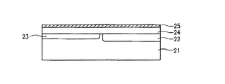
図1は、強誘電体膜、例えば、SBT膜、または、SBTN膜を誘電体とするキャパシタの製造方法を説明するための図面である。
【0005】
従来技術は、図1に示すように、ノード(図示しない)が形成された半導体基板11の上部に第1層間絶縁膜12を蒸着して形成する。
【0006】
次に、接着層13及び電荷蓄積電極用導電層14は層間絶縁膜12の上部に順次に蒸着する。その際、前記接着層13は、Ti、TiN、TiOx層が用いられ、電荷蓄積電極用導電層14は、例えば、Pt層が用いられる。
【0007】
次に、SBT膜15が電荷蓄積電極用導電層14の上部に蒸着され、プレート電極用導電層16をSBT膜15の上部に蒸着する。
【0008】
次に、図示していないが、後続工程を連続進行してキャパシタ製造工程を完了する。
【0009】
【発明が解決しようとする課題】
しかし、前記接着層のTi系の物質は、後続の下部電極上に形成されたSBT膜、SBTN膜中に、キャパシタ結晶化アニーリング過程で急激に拡散して、キャパシタの内部へ浸透して電気的特性を大いに劣化させる。
【0010】
また、結晶化アニーリング過程で下部電極を介して流入される酸素により接着層が酸化されて体積の増加により隙間が生じて、下部電極との界面で下部電極の再結晶化と、これに伴う流動性によりボイドと界面剥離(lifting)が生じて構造的にキャパシタの形成が難くなる。
【0011】
ここで、本発明は、前述の諸点に鑑みてなされたもので、その目的は、キャパシタの劣化を防止することができる不揮発性半導体メモリ素子のキャパシタ製造方法を提供することにある。
【0012】
【課題を解決するための手段】
本発明者は、不揮発性半導体メモリ素子のキャパシタ製造方法において、下部電極に使用される接着層としてTaON薄膜を使用することにより、強誘電体膜用SBT、または、SBTN膜キャパシタのぺロブスカイト構造を含むキャパシタの劣化が生じず、構造的にも安定しているので、後続の工程でに流入される酸素により酸化されてもTa2O5が安定している化合物を形成して、構造的にも安定し、表面が柔らかくて界面特性も良好であることを見いだし、本発明を完成した。
【0013】
即ち、前記の目的の達成のための本発明は、フィールド酸化膜と接合領域が形成された半導体基板を提供するステップと、前記半導体基板上に第1の層間絶縁膜を形成するステップと、前記第1の層間絶縁膜の上部に接着層用TaON薄膜を形成するステップと、前記TaON薄膜の上部に下部電極を形成するステップと、前記下部電極の上部に強誘電体薄膜用SBT、または、SBTN膜を形成するステップと、前記強誘電体薄膜の上部に上部電極を形成するステップと、接合領域と上部電極とのコンタクトのためのコンタクトホールを備える第3の層間絶縁膜を形成するステップと、前記コンタクトホールが埋め込まれるように金属膜を形成するステップとを含んでなることを特徴とする。
【0014】
【発明の実施の形態】
以下、図面を参照しながら本発明にかかる不揮発性メモリ素子のキャパシタ製造方法を詳細に説明する。
【0015】
本発明にかかる不揮発性メモリ素子のキャパシタ製造方法は、図2Aに示すように、フィールド酸化膜22を周知の方法により半導体基板21の所定部分に形成する。
【0016】
次に、ゲート絶縁膜を含むゲート電極(図示しない)を半導体基板21及びフィールド酸化膜22の所定部分に形成する。
【0017】
次に、側壁スペーサ(図示しない)は、ゲート電極の両側壁に周知の方式により形成され、ゲート電極両側の半導体基板21に接合領域23を形成してトランジスタを形成する。
【0018】
次に、前記のようにして得られた構造物の上部に第1層間絶縁膜24を蒸着した後、CMP工程を行って平坦化する。
【0019】
次に、図2Bに示すように、前記第1層間絶縁膜24の上部に接着層用TaON薄膜25を蒸着する。
【0020】
その際、接着層用TaON薄膜25は、CVD、または、PE−CVD(prasma enhanced CVD)、PVD、ALD(Atomic Layer Deposition)方式などにより形成される。ここで、接着層用TaON薄膜25は、タンタルエチレート(Ta(OC2H5)5)を原料物質として用いて、100mTorrないし10Torr(13.3ないし1330Pa)の圧力範囲内でNH3ガスが供給されるチャンバ内で、50〜400Åの厚さとなるように形成される。前記CVD方式は、400〜700℃の蒸着温度で進行してTaON薄膜25を形成し、PE−CVD方式は、200〜500℃の蒸着温度で200〜1000ワットのプラズマパワーを印加してTaON薄膜25を形成する。
【0021】
また、前記接着層用TaON薄膜25は、強誘電体膜用SBT、または、SBTN膜キャパシタのぺロブスカイト構造を含むキャパシタの劣化を生じさせず、構造的にも安定しているので、後続の工程で流入される酸素により酸化されてもTa2O5が安定している化合物を形成し、構造的にも安定し、表面が柔らかくて界面特性も良好である。
【0022】
次に、図2Cに示すように、前記TaON薄膜25の上部に下部電極用金属膜26を蒸着する。前記下部電極用金属膜26は、例えば、Pt、Ir、IrOx、Ru、または、RuOx膜からなり、蒸着方式としては、CVD、PE−CVD、PVD、または、ALD(Atomic Layer Deposition)方式を用いて形成する。また、前記下部電極用金属膜26は、500〜3000Åの厚さに形成するのが望ましい。
【0023】
次に、前記下部電極用金属膜26の上部に強誘電体膜用SBT、または、SBTN膜27を蒸着する。前記強誘電体薄膜用SBT、または、SBTN膜は、昇温速度が80〜300℃/secであり、O2、N2O、または、O2+N2ガスを反応ガスとして用いるRTP処理により核を生成し、続いて、700〜850℃の温度及びO2、N2O、または、O2+N2ガスを反応ガスとして用いるファーネスガス熱処理(furnace thermal treatment)を行って、結晶粒成長を促進することにより形成することができる。
【0024】
また、別の実施の形態の形成方法としては、スピン−オン、スパッタリングなどのPVDスパッタリング、PE−MOCVD等、多様な成膜方式を用いてキャパシタを形成する。
【0025】
前記スピン−オン方式は、ストロンチウム、ビスマス等を、オクタンとそれぞれ別々に混合することにより、液体原料として使用し、かつ、Sr、Biなどの安定剤としてN−ブチルアセテート(n-butyl acetate)を用いて、SBT、または、SBTN膜を形成する。ビスマス、ストロンチウム等は、粉末状のものをオクタンに分散させて用いる。
【0026】
その際、前記液体原料中、ストロンチウムとオクタンとの混合液としては0.7〜1.0(mole%)程度のものを用いて、前記ビスマスとオクタンとの混合液は、2.05〜2.5(mole%)程度のものを用いる。
【0027】
さらに、前記PVDスパッタリング方式は、常温で薄膜を蒸着形成し、膜の組成を均質化するためにRTA処理を行った後、後続の熱処理により結晶粒の成長を促進する。
【0028】
また、前記PE−MOCVD方式は、蒸着圧力が5mTorr 〜50Torr(0.665〜6650Pa)で400〜700℃の温度で行い、強誘電体薄膜用SBT、または、SBTN膜を形成する。
【0029】
強誘電体薄膜用SBT、または、SBTN膜は、上記に例示した種々の方法によって、通常、膜厚が100〜3000Å程度となるように形成される。
【0030】
次に、前記強誘電体薄膜用SBT、または、SBTN膜27の上部に上部電極用金属膜28を300〜3000Å程度の膜厚となるように蒸着する。
【0031】
次に、図2Dに示すように、前記上部電極用金属膜の上部にハードマスク膜を蒸着し、キャパシタ形成領域に感光膜パターン(図示しない)を形成する。
【0032】
次に、前記感光膜パターンをエッチング障壁にして、ハードマスク膜29をエッチングする。
【0033】
次に、図2Eに示すように、前記ハードマスク膜29をエッチング障壁にして前記上部電極用金属膜28、強誘電体薄膜27、下部電極用金属膜26と接着層用TaON薄膜25を順次エッチングし、キャパシタを形成する。
【0034】
次に、前記ハードマスク膜29を除去し、前記結果物の上部に第2層間絶縁膜30を蒸着する。
【0035】
次に、図2Fに示すように、前記接合領域23と上部電極用金属膜28の所定部分が露出されるように、第2層間絶縁膜をエッチングし、コンタクトホール(図示しない)を形成し、前記コンタクトホールが埋め込まれるように金属膜31を蒸着して不揮発性半導体素子のキャパシタを完成する。
【0036】
【発明の効果】
前述のように、本発明にかかる不揮発性半導体メモリ素子のキャパシタ製造方法は、下部電極に使用される接着層としてTaON薄膜を使用したので、強誘電体膜用SBT、または、SBTN膜キャパシタのぺロブスカイト構造を含むキャパシタの劣化が生じず、構造的にも安定しているので、後続の工程でに流入される酸素により酸化されてもTa2O5が安定している化合物を形成して、構造的にも安定し、表面が柔らかくて界面特性も良好である。
【0037】
これによって、キャパシタの下部電極に使用される接着層としてTaON薄膜を使用することにより、接触特性を向上させ、下部電極との界面剥離を抑えて電気的特性を向上させる効果がある。
【0038】
また、本発明は、その要旨を外れない範囲内で各種変形が可能である。
【図面の簡単な説明】
【図1】従来の不揮発性半導体メモリ素子のキャパシタ製造方法を説明するための断面図である。
【図2A】図2Aは、本発明の不揮発性半導体メモリ素子のキャパシタ製造方法を説明するための断面図の一つであり図2Bに続く。
【図2B】図2Bは、本発明の不揮発性半導体メモリ素子のキャパシタ製造方法を説明するための断面図の一つであり図2Cに続く。
【図2C】図2Cは、本発明の不揮発性半導体メモリ素子のキャパシタ製造方法を説明するための断面図の一つであり図2Dに続く。
【図2D】図2Dは、本発明の不揮発性半導体メモリ素子のキャパシタ製造方法を説明するための断面図の一つであり図2Eに続く。
【図2E】図2Eは、本発明の不揮発性半導体メモリ素子のキャパシタ製造方法を説明するための断面図の一つであり図2Fに続く。
【図2F】図2Fは、本発明の不揮発性半導体メモリ素子のキャパシタ製造方法を説明するための断面図の一つである。
【符号の説明】
11、21 半導体基板
12、24 第1層間絶縁膜
13 接着層
14 電極用導電層
15 SBT膜
16 プレート電極用導電層
22 フィールド酸化膜
23 接合領域
25 TaON薄膜
26 下部電極用金属膜
27 強誘電体薄膜(SBTN膜又はSBT膜)
28 上部電極用金属膜
29 ハードマスク膜
30 第2層間絶縁膜
31 金属膜[0001]
[Technical field to which the invention belongs]
The present invention relates to a method for manufacturing a capacitor of a nonvolatile semiconductor memory device, and more particularly to a method for manufacturing a capacitor for stabilizing a lower electrode of a ferroelectric film.
[0002]
[Prior art]
In general, since a ferroelectric memory device is nonvolatile, the stored contents are not erased even after the power is turned off. When the thickness of the ferroelectric film is sufficiently thin, the reversal of spontaneous polarization is accelerated, and reading and writing can be performed at high speed as in a DRAM.
[0003]
Further, a 1-bit memory cell can be formed as one transistor and one ferroelectric capacitor, which is applied to a large capacity. Such ferroelectric films include Sr x Bi 2 + y Ta 2 O 9 (SBT) film, Sr x Bi 2 + y (Ta i Nb 1-i ) 2 O 9 (SBTN) film, and the like.
[0004]
FIG. 1 is a drawing for explaining a method of manufacturing a capacitor using a ferroelectric film, for example, an SBT film or an SBTN film as a dielectric.
[0005]
In the prior art, as shown in FIG. 1, a first interlayer
[0006]
Next, the
[0007]
Next, the SBT
[0008]
Next, although not shown, the subsequent steps are continuously advanced to complete the capacitor manufacturing process.
[0009]
[Problems to be solved by the invention]
However, the Ti-based material of the adhesive layer diffuses rapidly in the capacitor crystallization annealing process in the SBT film and SBTN film formed on the subsequent lower electrode and penetrates into the capacitor to be electrically The characteristics are greatly degraded.
[0010]
In addition, the adhesive layer is oxidized by oxygen flowing through the lower electrode during the crystallization annealing process, and a gap is generated due to the increase in volume, and the recrystallization of the lower electrode at the interface with the lower electrode and the accompanying flow Due to the properties, voids and interface peeling occur, and it is structurally difficult to form a capacitor.
[0011]
The present invention has been made in view of the above-described points, and an object of the present invention is to provide a method for manufacturing a capacitor of a nonvolatile semiconductor memory element that can prevent deterioration of the capacitor.
[0012]
[Means for Solving the Problems]
The present inventor has developed a perovskite structure of an SBT for a ferroelectric film or an SBTN film capacitor by using a TaON thin film as an adhesive layer used for a lower electrode in a method for manufacturing a capacitor of a nonvolatile semiconductor memory device. Since the capacitor including the capacitor does not deteriorate and is structurally stable, a compound in which Ta 2 O 5 is stable even when oxidized by oxygen flowing in the subsequent process is formed structurally. The present invention has been completed by finding that it is stable, has a soft surface and good interfacial properties.
[0013]
That is, the present invention for achieving the above object includes a step of providing a semiconductor substrate in which a field oxide film and a junction region are formed, a step of forming a first interlayer insulating film on the semiconductor substrate, Forming a TaON thin film for an adhesive layer on the first interlayer insulating film; forming a lower electrode on the TaON thin film; and an SBT for ferroelectric thin film or SBTN on the lower electrode. Forming a film; forming an upper electrode on the ferroelectric thin film; forming a third interlayer insulating film having a contact hole for contact between the junction region and the upper electrode; Forming a metal film so as to fill the contact hole.
[0014]
DETAILED DESCRIPTION OF THE INVENTION
Hereinafter, a method for manufacturing a capacitor of a nonvolatile memory device according to the present invention will be described in detail with reference to the drawings.
[0015]
In the method for manufacturing a capacitor of a nonvolatile memory device according to the present invention, as shown in FIG. 2A, a
[0016]
Next, a gate electrode (not shown) including a gate insulating film is formed on predetermined portions of the
[0017]
Next, sidewall spacers (not shown) are formed on both side walls of the gate electrode by a well-known method, and a
[0018]
Next, a first
[0019]
Next, as shown in FIG. 2B, an adhesive layer TaON
[0020]
At that time, the TaON
[0021]
Further, the TaON
[0022]
Next, as shown in FIG. 2C, a lower
[0023]
Next, an SBT for ferroelectric film or an
[0024]
In another embodiment, the capacitor is formed using various film formation methods such as spin-on, PVD sputtering such as sputtering, PE-MOCVD, and the like.
[0025]
The spin-on method uses strontium, bismuth, etc. separately from octane as a liquid raw material, and N-butyl acetate as a stabilizer such as Sr, Bi. The SBT or SBTN film is formed by using this. Bismuth, strontium, etc. are used in a powder form dispersed in octane.
[0026]
At that time, in the liquid raw material, a mixture of strontium and octane is about 0.7 to 1.0 (mole%), and the mixture of bismuth and octane is 2.05 to 2. About 5 (mole%) is used.
[0027]
Furthermore, the PVD sputtering method promotes the growth of crystal grains by subsequent heat treatment after depositing and forming a thin film at room temperature, performing RTA treatment to homogenize the composition of the film.
[0028]
The PE-MOCVD method is performed at a deposition pressure of 5 mTorr to 50 Torr (0.665 to 6650 Pa) at a temperature of 400 to 700 ° C. to form an SBT for a ferroelectric thin film or an SBTN film.
[0029]
The SBT for ferroelectric thin film or the SBTN film is usually formed to have a film thickness of about 100 to 3000 mm by the various methods exemplified above.
[0030]
Next, the upper
[0031]
Next, as shown in FIG. 2D, a hard mask film is deposited on the upper electrode metal film to form a photosensitive film pattern (not shown) in the capacitor formation region.
[0032]
Next, the
[0033]
Next, as shown in FIG. 2E, the upper
[0034]
Next, the
[0035]
Next, as shown in FIG. 2F, the second interlayer insulating film is etched so that predetermined portions of the
[0036]
【The invention's effect】
As described above, the method for manufacturing a capacitor of a nonvolatile semiconductor memory device according to the present invention uses a TaON thin film as an adhesive layer used for the lower electrode, so that the SBT for a ferroelectric film or the SBTN film capacitor is used. Since the capacitor including the lobskite structure does not deteriorate and is structurally stable, a compound in which Ta 2 O 5 is stable even when oxidized by oxygen flowing into the subsequent process is formed. The structure is stable, the surface is soft, and the interface characteristics are good.
[0037]
As a result, the TaON thin film is used as an adhesive layer used for the lower electrode of the capacitor, thereby improving the contact characteristics and suppressing the interface peeling with the lower electrode, thereby improving the electrical characteristics.
[0038]
The present invention can be modified in various ways within the scope of the invention.
[Brief description of the drawings]
FIG. 1 is a cross-sectional view for explaining a conventional method for manufacturing a capacitor of a nonvolatile semiconductor memory device.
FIG. 2A is one of cross-sectional views for explaining a method of manufacturing a capacitor of a nonvolatile semiconductor memory device according to the present invention, and is continued from FIG. 2B.
FIG. 2B is one of cross-sectional views for explaining a method for manufacturing a capacitor of a nonvolatile semiconductor memory device of the present invention, and is continued from FIG. 2C.
FIG. 2C is one of cross-sectional views for explaining a method of manufacturing a capacitor of a nonvolatile semiconductor memory device according to the present invention, and is continued from FIG. 2D.
FIG. 2D is a cross-sectional view illustrating a method for manufacturing a capacitor of a nonvolatile semiconductor memory device according to the present invention, and is a continuation of FIG. 2E.
FIG. 2E is a cross-sectional view illustrating a method for manufacturing a capacitor of a nonvolatile semiconductor memory element according to the present invention, which is continued from FIG. 2F.
FIG. 2F is a cross-sectional view illustrating a method for manufacturing a capacitor of a nonvolatile semiconductor memory element according to the present invention.
[Explanation of symbols]
11, 21
28 Metal film for
Claims (14)
前記TaON接着層の上部に下部電極を形成するステップと、
前記下部電極の上部にSBT、または、SBTN膜からなる強誘電体膜を形成するステップと、
前記強誘電体膜上に上部電極を形成するステップ
とを含んでなることを特徴とする不揮発性半導体メモリ素子のキャパシタ製造方法。Forming a TaON adhesive layer on the semiconductor substrate;
Forming a lower electrode on top of the TaON adhesive layer;
Forming a ferroelectric film made of SBT or SBTN film on the lower electrode;
Forming a top electrode on the ferroelectric film; and a method of manufacturing a capacitor of a nonvolatile semiconductor memory device.
Applications Claiming Priority (2)
| Application Number | Priority Date | Filing Date | Title |
|---|---|---|---|
| KR10-2000-0036812A KR100372644B1 (en) | 2000-06-30 | 2000-06-30 | Method for manufacturing capacitor in nonvolatile semiconductor memory device |
| KR2000-36812 | 2000-06-30 |
Publications (2)
| Publication Number | Publication Date |
|---|---|
| JP2002110939A JP2002110939A (en) | 2002-04-12 |
| JP4140214B2 true JP4140214B2 (en) | 2008-08-27 |
Family
ID=19675121
Family Applications (1)
| Application Number | Title | Priority Date | Filing Date |
|---|---|---|---|
| JP2001189273A Expired - Fee Related JP4140214B2 (en) | 2000-06-30 | 2001-06-22 | Capacitor manufacturing method for nonvolatile semiconductor memory device |
Country Status (3)
| Country | Link |
|---|---|
| US (2) | US6597029B2 (en) |
| JP (1) | JP4140214B2 (en) |
| KR (1) | KR100372644B1 (en) |
Families Citing this family (18)
| Publication number | Priority date | Publication date | Assignee | Title |
|---|---|---|---|---|
| KR100504554B1 (en) * | 2000-12-21 | 2005-08-01 | 주식회사 하이닉스반도체 | method for manufacturing capacitor of semiconductor device |
| US6908639B2 (en) * | 2001-04-02 | 2005-06-21 | Micron Technology, Inc. | Mixed composition interface layer and method of forming |
| KR100476556B1 (en) * | 2002-04-11 | 2005-03-18 | 삼성전기주식회사 | Piezoelectric transformer, housing for piezoelectric transformer and manufacture thereof |
| US7264846B2 (en) * | 2002-06-04 | 2007-09-04 | Applied Materials, Inc. | Ruthenium layer formation for copper film deposition |
| US7910165B2 (en) * | 2002-06-04 | 2011-03-22 | Applied Materials, Inc. | Ruthenium layer formation for copper film deposition |
| US7404985B2 (en) * | 2002-06-04 | 2008-07-29 | Applied Materials, Inc. | Noble metal layer formation for copper film deposition |
| JP4308485B2 (en) * | 2002-07-08 | 2009-08-05 | パナソニック株式会社 | Capacitor element manufacturing method |
| US20050181226A1 (en) * | 2004-01-26 | 2005-08-18 | Applied Materials, Inc. | Method and apparatus for selectively changing thin film composition during electroless deposition in a single chamber |
| US20050253268A1 (en) * | 2004-04-22 | 2005-11-17 | Shao-Ta Hsu | Method and structure for improving adhesion between intermetal dielectric layer and cap layer |
| JP5281746B2 (en) * | 2004-05-14 | 2013-09-04 | ルネサスエレクトロニクス株式会社 | Semiconductor memory device |
| US7429402B2 (en) * | 2004-12-10 | 2008-09-30 | Applied Materials, Inc. | Ruthenium as an underlayer for tungsten film deposition |
| US7265048B2 (en) * | 2005-03-01 | 2007-09-04 | Applied Materials, Inc. | Reduction of copper dewetting by transition metal deposition |
| US20070099422A1 (en) * | 2005-10-28 | 2007-05-03 | Kapila Wijekoon | Process for electroless copper deposition |
| US20070128862A1 (en) * | 2005-11-04 | 2007-06-07 | Paul Ma | Apparatus and process for plasma-enhanced atomic layer deposition |
| US7833358B2 (en) * | 2006-04-07 | 2010-11-16 | Applied Materials, Inc. | Method of recovering valuable material from exhaust gas stream of a reaction chamber |
| TWI395335B (en) * | 2006-06-30 | 2013-05-01 | Applied Materials Inc | Nanocrystal formation |
| US7737028B2 (en) * | 2007-09-28 | 2010-06-15 | Applied Materials, Inc. | Selective ruthenium deposition on copper materials |
| CN110904419A (en) * | 2019-12-18 | 2020-03-24 | 厦门佰事兴新材料科技有限公司 | Electrolytic anode plate and preparation method thereof |
Family Cites Families (12)
| Publication number | Priority date | Publication date | Assignee | Title |
|---|---|---|---|---|
| JPH0714993A (en) * | 1993-06-18 | 1995-01-17 | Mitsubishi Electric Corp | Semiconductor device and manufacturing thereof |
| US5612574A (en) * | 1995-06-06 | 1997-03-18 | Texas Instruments Incorporated | Semiconductor structures using high-dielectric-constant materials and an adhesion layer |
| KR970018537A (en) * | 1995-09-21 | 1997-04-30 | 김광호 | Capacitor Formation Method for Semiconductor Device |
| US5874770A (en) * | 1996-10-10 | 1999-02-23 | General Electric Company | Flexible interconnect film including resistor and capacitor layers |
| US6130103A (en) * | 1998-04-17 | 2000-10-10 | Symetrix Corporation | Method for fabricating ferroelectric integrated circuits |
| US6139780A (en) * | 1998-05-28 | 2000-10-31 | Sharp Kabushiki Kaisha | Dynamic random access memories with dielectric compositions stable to reduction |
| KR100399886B1 (en) * | 1998-07-02 | 2004-02-11 | 주식회사 하이닉스반도체 | Capacitor Formation Method of Semiconductor Memory Device |
| US6201276B1 (en) * | 1998-07-14 | 2001-03-13 | Micron Technology, Inc. | Method of fabricating semiconductor devices utilizing in situ passivation of dielectric thin films |
| JP2000049116A (en) * | 1998-07-30 | 2000-02-18 | Toshiba Corp | Semiconductor device and manufacture of the same |
| JP2000068465A (en) * | 1998-08-21 | 2000-03-03 | Nec Corp | Semiconductor device and method for forming the same |
| KR100326242B1 (en) * | 1998-10-24 | 2002-08-21 | 주식회사 하이닉스반도체 | A method for forming capacitor in semiconductor device |
| KR100331270B1 (en) * | 1999-07-01 | 2002-04-06 | 박종섭 | Forming method of capacitor with TaON thin film |
-
2000
- 2000-06-30 KR KR10-2000-0036812A patent/KR100372644B1/en not_active IP Right Cessation
-
2001
- 2001-06-14 US US09/880,056 patent/US6597029B2/en not_active Expired - Fee Related
- 2001-06-22 JP JP2001189273A patent/JP4140214B2/en not_active Expired - Fee Related
-
2003
- 2003-06-03 US US10/452,494 patent/US6815225B2/en not_active Expired - Lifetime
Also Published As
| Publication number | Publication date |
|---|---|
| KR100372644B1 (en) | 2003-02-17 |
| KR20020002597A (en) | 2002-01-10 |
| JP2002110939A (en) | 2002-04-12 |
| US20020000587A1 (en) | 2002-01-03 |
| US20030205744A1 (en) | 2003-11-06 |
| US6597029B2 (en) | 2003-07-22 |
| US6815225B2 (en) | 2004-11-09 |
Similar Documents
| Publication | Publication Date | Title |
|---|---|---|
| JP4140214B2 (en) | Capacitor manufacturing method for nonvolatile semiconductor memory device | |
| JPH1154718A (en) | Integrated circuit device having buffer film constituted of metal oxide film which is stabilized by low temperature treatment, and its manufacture | |
| JP2003007859A (en) | Method for manufacturing memory device having dielectric film | |
| KR100476375B1 (en) | Capacitor and method for fabricating nonvolatile device with the same | |
| JP2003218325A (en) | Ferroelectric film forming method and semiconductor device manufacturing method | |
| JP2000260954A (en) | Ferroelectrics capacitor, semiconductor device, and manufacture thereof | |
| JP2001237402A (en) | Structured metal oxide containing layer, and method of manufacturing semiconductor structure element | |
| JP2000223666A (en) | Fabrication of semiconductor memory element | |
| CN1954430B (en) | Semiconductor device and process for fabricating same | |
| JP2011124497A (en) | Semiconductor device and method of manufacturing the same | |
| KR100614576B1 (en) | Method for forming capacitor | |
| KR100443362B1 (en) | Method for fabricating capacitor with 2 step annealing in semiconductor device | |
| JP2007184442A (en) | Ferroelectric capacitor | |
| KR100436054B1 (en) | Method for fabricating ferroelectric capacitor to increase remnant polarization and improve reliability related with fatigue, leakage current and data retention | |
| KR100353809B1 (en) | Method for manufacturing ferroelectric capacitor | |
| KR100388465B1 (en) | Ferroelectric capacitor having ruthenium bottom electrode and forming method thereof | |
| JP2003152167A (en) | Capacitor of semiconductor element and its manufacturing method | |
| KR100448242B1 (en) | Method for fabricating capacitor top electrode in semiconductor device | |
| JP2002151659A (en) | Semiconductor device and manufacturing method therefor | |
| KR100471400B1 (en) | Method for forming Bismuth-base ferroelectric layer | |
| KR100388467B1 (en) | A method of forming BLT layer in semiconductor device | |
| KR100869339B1 (en) | Method for forming Bismuth-base ferroelectric layer | |
| KR100388466B1 (en) | Ferroelectric capacitor having ruthenium bottom electrode and forming method thereof | |
| KR100470159B1 (en) | Ferroelectric Random Access Memory having Iridium plug and method for fabricating the same | |
| JP2001077326A (en) | Semiconductor device and its manufacturing method |
Legal Events
| Date | Code | Title | Description |
|---|---|---|---|
| A621 | Written request for application examination |
Free format text: JAPANESE INTERMEDIATE CODE: A621 Effective date: 20051209 |
|
| A977 | Report on retrieval |
Free format text: JAPANESE INTERMEDIATE CODE: A971007 Effective date: 20080428 |
|
| TRDD | Decision of grant or rejection written | ||
| A01 | Written decision to grant a patent or to grant a registration (utility model) |
Free format text: JAPANESE INTERMEDIATE CODE: A01 Effective date: 20080507 |
|
| A01 | Written decision to grant a patent or to grant a registration (utility model) |
Free format text: JAPANESE INTERMEDIATE CODE: A01 |
|
| A61 | First payment of annual fees (during grant procedure) |
Free format text: JAPANESE INTERMEDIATE CODE: A61 Effective date: 20080602 |
|
| FPAY | Renewal fee payment (event date is renewal date of database) |
Free format text: PAYMENT UNTIL: 20110620 Year of fee payment: 3 |
|
| R150 | Certificate of patent or registration of utility model |
Free format text: JAPANESE INTERMEDIATE CODE: R150 |
|
| FPAY | Renewal fee payment (event date is renewal date of database) |
Free format text: PAYMENT UNTIL: 20120620 Year of fee payment: 4 |
|
| FPAY | Renewal fee payment (event date is renewal date of database) |
Free format text: PAYMENT UNTIL: 20130620 Year of fee payment: 5 |
|
| LAPS | Cancellation because of no payment of annual fees |